Embed Size (px)
Citation preview
www.ti.com
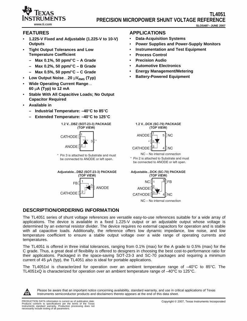
FEATURES APPLICATIONS
* Pin 3 is attached to Substrate and mustbe connected to ANODE or left open.
CATHODE
ANODE
*
1
2
3
FB
CATHODE
ANODE
1
2
3
1.2 V...DBZ (SOT-23-3) PACKAGE(TOP VIEW)
Adjustable...DBZ (SOT-23-3) PACKAGE(TOP VIEW)
NC – No internal connection
NC
NC
1
2
3
5
4
FB
ANODE
CATHODE
* Pin 2 is attached to Substrate and mustbe connected to ANODE or left open.
ANODE NC1
2
3
5
4 NCCATHODE
*
Adjustable...DCK (SC-70) PACKAGE(TOP VIEW)
1.2 V...DCK (SC-70) PACKAGE(TOP VIEW)
NC – No internal connection
DESCRIPTION/ORDERING INFORMATION
TL4051PRECISION MICROPOWER SHUNT VOLTAGE REFERENCE
SLOS487–JUNE 2007
• Data-Acquisition Systems• 1.225-V Fixed and Adjustable (1.225-V to 10-V)Outputs • Power Supplies and Power-Supply Monitors
• Instrumentation and Test Equipment• Tight Output Tolerances and LowTemperature Coefficient • Process Control
• Precision Audio– Max 0.1%, 50 ppm/°C – A Grade• Automotive Electronics– Max 0.2%, 50 ppm/°C – B Grade• Energy Management/Metering– Max 0.5%, 50 ppm/°C – C Grade• Battery-Powered Equipment• Low Output Noise…20 µVRMS (Typ)
• Wide Operating Current Range…60 µA (Typ) to 12 mA
• Stable With All Capacitive Loads; No OutputCapacitor Required
• Available in– Industrial Temperature: –40°C to 85°C– Extended Temperature: –40°C to 125°C
The TL4051 series of shunt voltage references are versatile easy-to-use references suitable for a wide array ofapplications. The device is available in a fixed 1.225-V output or an adjustable output whose voltage isdetermined by an external resistor divider. The device requires no external capacitors for operation and is stablewith all capacitive loads. Additionally, the reference offers low dynamic impedance, low noise, and lowtemperature coefficient to ensure a stable output voltage over a wide range of operating currents andtemperatures.
The TL4051 is offered in three initial tolerances, ranging from 0.1% (max) for the A grade to 0.5% (max) for theC grade. Thus, a great deal of flexibility is offered to designers in choosing the best cost-to-performance ratio fortheir applications. Packaged in the space-saving SOT-23-3 and SC-70 packages and requiring a minimumcurrent of 45 µA (typ), the TL4051 also is ideal for portable applications.
The TL4051xI is characterized for operation over an ambient temperature range of –40°C to 85°C. TheTL4051xQ is characterized for operation over an ambient temperature range of –40°C to 125°C.
Please be aware that an important notice concerning availability, standard warranty, and use in critical applications of TexasInstruments semiconductor products and disclaimers thereto appears at the end of this data sheet.
PRODUCTION DATA information is current as of publication date. Copyright © 2007, Texas Instruments IncorporatedProducts conform to specifications per the terms of the TexasInstruments standard warranty. Production processing does notnecessarily include testing of all parameters.
www.ti.com
TL4051PRECISION MICROPOWER SHUNT VOLTAGE REFERENCESLOS487–JUNE 2007
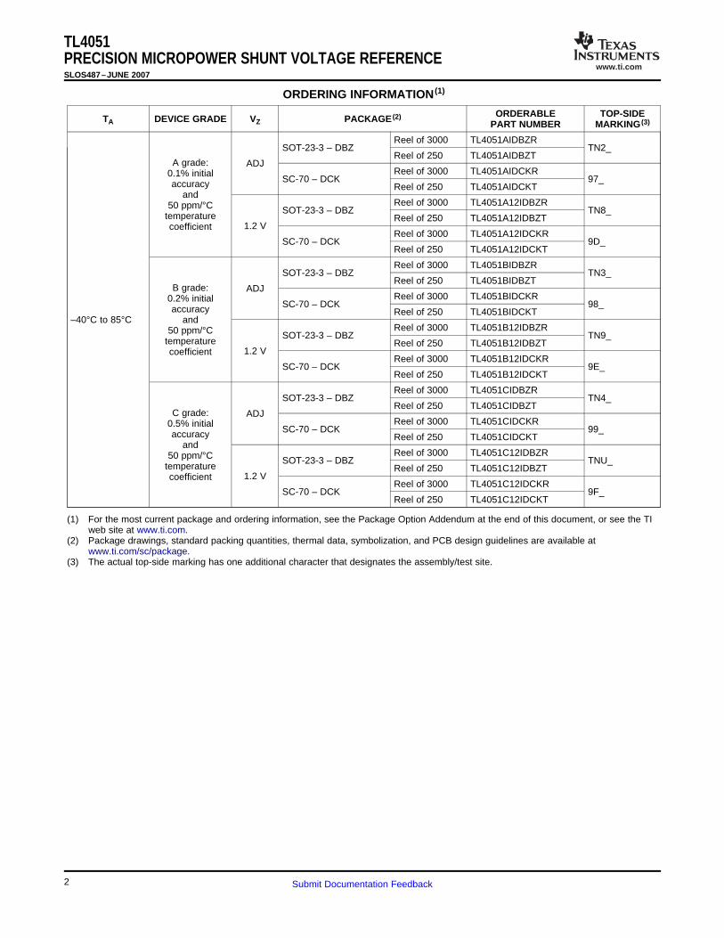
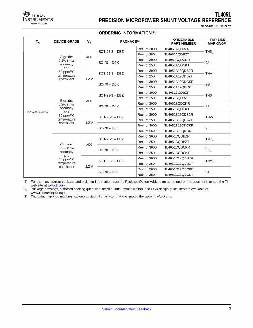
ORDERING INFORMATION (1)
ORDERABLE TOP-SIDETA DEVICE GRADE VZ PACKAGE (2)PART NUMBER MARKING (3)
Reel of 3000 TL4051AIDBZRSOT-23-3 – DBZ TN2_
Reel of 250 TL4051AIDBZTA grade: ADJ
Reel of 3000 TL4051AIDCKR0.1% initialSC-70 – DCK 97_accuracy Reel of 250 TL4051AIDCKT
andReel of 3000 TL4051A12IDBZR50 ppm/°C SOT-23-3 – DBZ TN8_
temperature Reel of 250 TL4051A12IDBZT1.2 Vcoefficient
Reel of 3000 TL4051A12IDCKRSC-70 – DCK 9D_
Reel of 250 TL4051A12IDCKT
Reel of 3000 TL4051BIDBZRSOT-23-3 – DBZ TN3_
Reel of 250 TL4051BIDBZTB grade: ADJ
Reel of 3000 TL4051BIDCKR0.2% initialSC-70 – DCK 98_accuracy Reel of 250 TL4051BIDCKT
–40°C to 85°C andReel of 3000 TL4051B12IDBZR50 ppm/°C SOT-23-3 – DBZ TN9_
temperature Reel of 250 TL4051B12IDBZT1.2 Vcoefficient
Reel of 3000 TL4051B12IDCKRSC-70 – DCK 9E_
Reel of 250 TL4051B12IDCKT
Reel of 3000 TL4051CIDBZRSOT-23-3 – DBZ TN4_
Reel of 250 TL4051CIDBZTC grade: ADJ
Reel of 3000 TL4051CIDCKR0.5% initialSC-70 – DCK 99_accuracy Reel of 250 TL4051CIDCKT
andReel of 3000 TL4051C12IDBZR50 ppm/°C SOT-23-3 – DBZ TNU_
temperature Reel of 250 TL4051C12IDBZT1.2 Vcoefficient
Reel of 3000 TL4051C12IDCKRSC-70 – DCK 9F_
Reel of 250 TL4051C12IDCKT
(1) For the most current package and ordering information, see the Package Option Addendum at the end of this document, or see the TIweb site at www.ti.com.
(2) Package drawings, standard packing quantities, thermal data, symbolization, and PCB design guidelines are available atwww.ti.com/sc/package.
(3) The actual top-side marking has one additional character that designates the assembly/test site.
2 Submit Documentation Feedback
www.ti.com
TL4051PRECISION MICROPOWER SHUNT VOLTAGE REFERENCE
SLOS487–JUNE 2007
ORDERING INFORMATION (1)
ORDERABLE TOP-SIDETA DEVICE GRADE VZ PACKAGE (2)PART NUMBER MARKING (3)
Reel of 3000 TL4051AQDBZRSOT-23-3 – DBZ TN5_
Reel of 250 TL4051AQDBZTA grade: ADJ
Reel of 3000 TL4051AQDCKR0.1% initialSC-70 – DCK 9A_accuracy Reel of 250 TL4051AQDCKT
andReel of 3000 TL4051A12QDBZR50 ppm/°C SOT-23-3 – DBZ TNV_
temperature Reel of 250 TL4051A12QDBZT1.2 Vcoefficient
Reel of 3000 TL4051A12QDCKRSC-70 – DCK 9G_
Reel of 250 TL4051A12QDCKT
Reel of 3000 TL4051BQDBZRSOT-23-3 – DBZ TN6_
Reel of 250 TL4051BQDBZTB grade: ADJ
Reel of 3000 TL4051BQDCKR0.2% initialSC-70 – DCK 9B_accuracy Reel of 250 TL4051BQDCKT
–40°C to 125°C andReel of 3000 TL4051B12QDBZR50 ppm/°C SOT-23-3 – DBZ TNW_
temperature Reel of 250 TL4051B12QDBZT1.2 Vcoefficient
Reel of 3000 TL4051B12QDCKRSC-70 – DCK 9H_
Reel of 250 TL4051B12QDCKT
Reel of 3000 TL4051CQDBZRSOT-23-3 – DBZ TN7_
Reel of 250 TL4051CQDBZTC grade: ADJ
Reel of 3000 TL4051CQDCKR0.5% initialSC-70 – DCK 9C_accuracy Reel of 250 TL4051CQDCKT
andReel of 3000 TL4051C12QDBZR50 ppm/°C SOT-23-3 – DBZ TNY_
temperature Reel of 250 TL4051C12QDBZT1.2 Vcoefficient
Reel of 3000 TL4051C12QDCKRSC-70 – DCK 9J_
Reel of 250 TL4051C12QDCKT
(1) For the most current package and ordering information, see the Package Option Addendum at the end of this document, or see the TIweb site at www.ti.com.
(2) Package drawings, standard packing quantities, thermal data, symbolization, and PCB design guidelines are available atwww.ti.com/sc/package.
(3) The actual top-side marking has one additional character that designates the assembly/test site.
3Submit Documentation Feedback
www.ti.com
CATHODE
ANODE
_
+
FB(see Note A)
V
(see Note A)REF
SeeNote B
SeeNote B
Absolute Maximum Ratings (1)
Recommended Operating Conditions
TL4051PRECISION MICROPOWER SHUNT VOLTAGE REFERENCESLOS487–JUNE 2007
FUNCTIONAL BLOCK DIAGRAM
A. TL4051x (Adjustable) only
B. TL4051x12 only
over free-air temperature range (unless otherwise noted)
MIN MAX UNIT
VZ Continuous cathode voltage 15 V
IZ Continuous cathode current –10 20 mA
DBZ package 206θJA Package thermal impedance (2) (3) °C/W
DCK package 252
TJ Operating virtual junction temperature 150 °C
Tstg Storage temperature range –65 150 °C
(1) Stresses beyond those listed under Absolute Maximum Ratings may cause permanent damage to the device. These are stress ratingsonly, and functional operation of the device at these or any other conditions beyond those indicated under Recommended OperatingConditions is not implied. Exposure to absolute-maximum-rated conditions for extended periods may affect device reliability.
(2) Maximum power dissipation is a function of TJ(max), θJA, and TA. The maximum allowable power dissipation at any allowable ambienttemperature is PD = (TJ(max) – TA)/θJA. Operating at the absolute maximum TJ of 150°C can affect reliability.
(3) The package thermal impedance is calculated in accordance with JESD 51-7.
MIN MAX UNIT
IZ Cathode current (1) 12 mA
VZ Reverse breakdown voltage (adjustable version) 10 V
I temperature –40 85TA Free-air temperature °C
Q temperature –40 125
(1) See parametric tables
4 Submit Documentation Feedback
www.ti.com
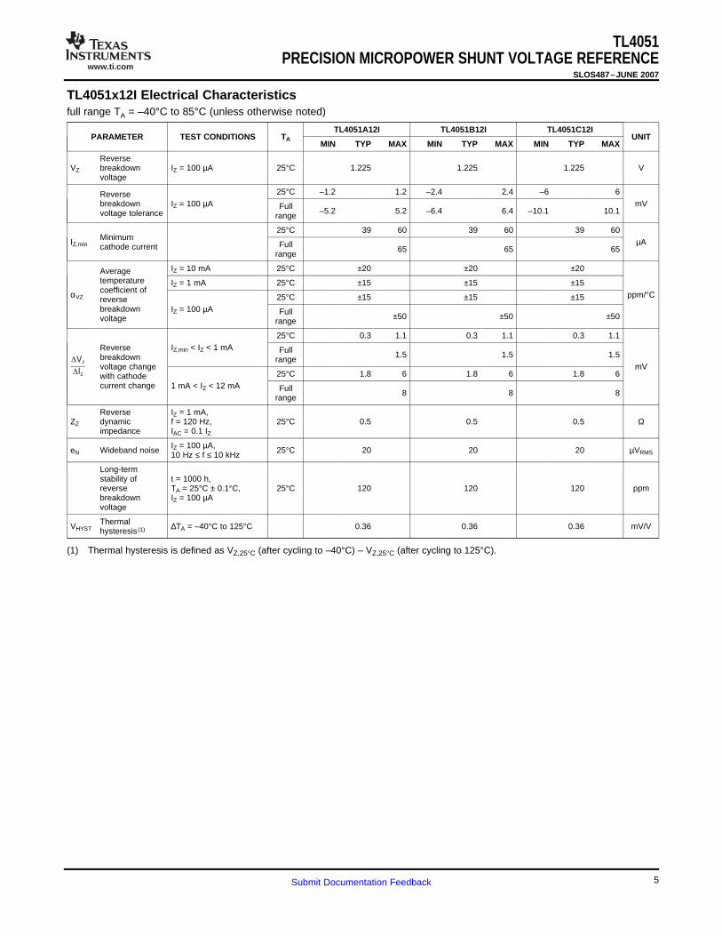
TL4051x12I Electrical Characteristics
DVZ
DIZ
TL4051PRECISION MICROPOWER SHUNT VOLTAGE REFERENCE
SLOS487–JUNE 2007
full range TA = –40°C to 85°C (unless otherwise noted)
TL4051A12I TL4051B12I TL4051C12IPARAMETER TEST CONDITIONS TA UNIT
MIN TYP MAX MIN TYP MAX MIN TYP MAX
ReverseVZ breakdown IZ = 100 µA 25°C 1.225 1.225 1.225 V
voltage
25°C –1.2 1.2 –2.4 2.4 –6 6Reversebreakdown IZ = 100 µA mVFull –5.2 5.2 –6.4 6.4 –10.1 10.1voltage tolerance range
25°C 39 60 39 60 39 60MinimumIZ,min µAFullcathode current 65 65 65range
IZ = 10 mA 25°C ±20 ±20 ±20Averagetemperature IZ = 1 mA 25°C ±15 ±15 ±15coefficient ofαVZ ppm/°C25°C ±15 ±15 ±15reversebreakdown IZ = 100 µA Full ±50 ±50 ±50voltage range
25°C 0.3 1.1 0.3 1.1 0.3 1.1IZ,min < IZ < 1 mAReverse Full 1.5 1.5 1.5breakdown range
voltage change mV25°C 1.8 6 1.8 6 1.8 6with cathode
current change 1 mA < IZ < 12 mA Full 8 8 8range
Reverse IZ = 1 mA,ZZ dynamic f = 120 Hz, 25°C 0.5 0.5 0.5 Ω
impedance IAC = 0.1 IZ
IZ = 100 µA,eN Wideband noise 25°C 20 20 20 µVRMS10 Hz ≤ f ≤ 10 kHz
Long-termstability of t = 1000 h,reverse TA = 25°C ± 0.1°C, 25°C 120 120 120 ppmbreakdown IZ = 100 µAvoltage
ThermalVHYST ∆TA = –40°C to 125°C 0.36 0.36 0.36 mV/Vhysteresis (1)
(1) Thermal hysteresis is defined as VZ,25°C (after cycling to –40°C) – VZ,25°C (after cycling to 125°C).
5Submit Documentation Feedback
www.ti.com
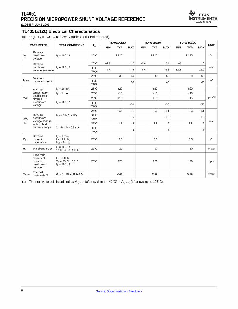
TL4051x12Q Electrical Characteristics
DVZ
DIZ
TL4051PRECISION MICROPOWER SHUNT VOLTAGE REFERENCESLOS487–JUNE 2007
full range TA = –40°C to 125°C (unless otherwise noted)
TL4051A12Q TL4051B12Q TL4051C12QPARAMETER TEST CONDITIONS TA UNIT
MIN TYP MAX MIN TYP MAX MIN TYP MAX
ReverseVZ breakdown IZ = 100 µA 25°C 1.225 1.225 1.225 V
voltage
25°C –1.2 1.2 –2.4 2.4 –6 6Reversebreakdown IZ = 100 µA mVFull –7.4 7.4 –8.6 8.6 –12.2 12.2voltage tolerance range
25°C 39 60 39 60 39 60MinimumIZ,min µAFullcathode current 65 65 65range
IZ = 10 mA 25°C ±20 ±20 ±20Averagetemperature IZ = 1 mA 25°C ±15 ±15 ±15coefficient ofαVZ ppm/°C25°C ±15 ±15 ±15reversebreakdown IZ = 100 µA Full ±50 ±50 ±50voltage range
25°C 0.3 1.1 0.3 1.1 0.3 1.1IZ,min < IZ < 1 mAReverse Full 1.5 1.5 1.5breakdown range
voltage change mV25°C 1.8 6 1.8 6 1.8 6with cathode
current change 1 mA < IZ < 12 mA Full 8 8 8range
Reverse IZ = 1 mA,ZZ dynamic f = 120 Hz, 25°C 0.5 0.5 0.5 Ω
impedance IAC = 0.1 IZ
IZ = 100 µA,eN Wideband noise 25°C 20 20 20 µVRMS10 Hz ≤ f ≤ 10 kHz
Long-termstability of t = 1000 h,reverse TA = 25°C ± 0.1°C, 25°C 120 120 120 ppmbreakdown IZ = 100 µAvoltage
ThermalVHYST ∆TA = –40°C to 125°C 0.36 0.36 0.36 mV/Vhysteresis (1)
(1) Thermal hysteresis is defined as VZ,25°C (after cycling to –40°C) – VZ,25°C (after cycling to 125°C).
6 Submit Documentation Feedback
www.ti.com
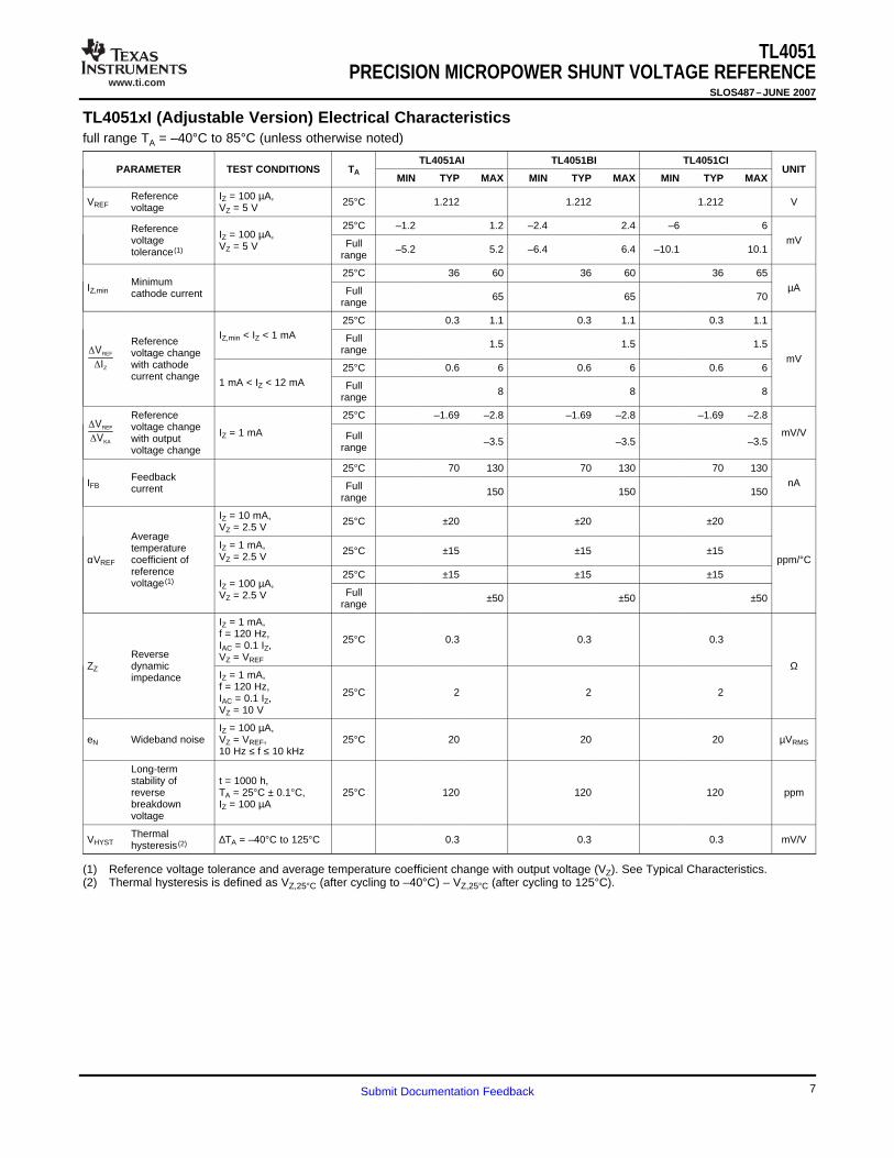
TL4051xI (Adjustable Version) Electrical Characteristics
DVREF
DIZ
DVREF
DVKA
TL4051PRECISION MICROPOWER SHUNT VOLTAGE REFERENCE
SLOS487–JUNE 2007
full range TA = –40°C to 85°C (unless otherwise noted)
TL4051AI TL4051BI TL4051CIPARAMETER TEST CONDITIONS TA UNIT
MIN TYP MAX MIN TYP MAX MIN TYP MAX
Reference IZ = 100 µA,VREF 25°C 1.212 1.212 1.212 Vvoltage VZ = 5 V
25°C –1.2 1.2 –2.4 2.4 –6 6Reference IZ = 100 µA,voltage mVFullVZ = 5 V –5.2 5.2 –6.4 6.4 –10.1 10.1tolerance (1) range
25°C 36 60 36 60 36 65MinimumIZ,min µAFullcathode current 65 65 70range
25°C 0.3 1.1 0.3 1.1 0.3 1.1IZ,min < IZ < 1 mA FullReference 1.5 1.5 1.5rangevoltage change mVwith cathode 25°C 0.6 6 0.6 6 0.6 6
current change1 mA < IZ < 12 mA Full 8 8 8range
Reference 25°C –1.69 –2.8 –1.69 –2.8 –1.69 –2.8voltage change IZ = 1 mA mV/VFullwith output –3.5 –3.5 –3.5rangevoltage change
25°C 70 130 70 130 70 130FeedbackIFB nAFullcurrent 150 150 150range
IZ = 10 mA, 25°C ±20 ±20 ±20VZ = 2.5 VAverage
IZ = 1 mA,temperature 25°C ±15 ±15 ±15VZ = 2.5 VαVREF coefficient of ppm/°Creference 25°C ±15 ±15 ±15voltage (1) IZ = 100 µA,
FullVZ = 2.5 V ±50 ±50 ±50range
IZ = 1 mA,f = 120 Hz, 25°C 0.3 0.3 0.3IAC = 0.1 IZ,
Reverse VZ = VREFZZ dynamic Ω
IZ = 1 mA,impedancef = 120 Hz, 25°C 2 2 2IAC = 0.1 IZ,VZ = 10 V
IZ = 100 µA,eN Wideband noise VZ = VREF, 25°C 20 20 20 µVRMS
10 Hz ≤ f ≤ 10 kHz
Long-termstability of t = 1000 h,reverse TA = 25°C ± 0.1°C, 25°C 120 120 120 ppmbreakdown IZ = 100 µAvoltage
ThermalVHYST ∆TA = –40°C to 125°C 0.3 0.3 0.3 mV/Vhysteresis (2)
(1) Reference voltage tolerance and average temperature coefficient change with output voltage (VZ). See Typical Characteristics.(2) Thermal hysteresis is defined as VZ,25°C (after cycling to –40°C) – VZ,25°C (after cycling to 125°C).
7Submit Documentation Feedback
www.ti.com
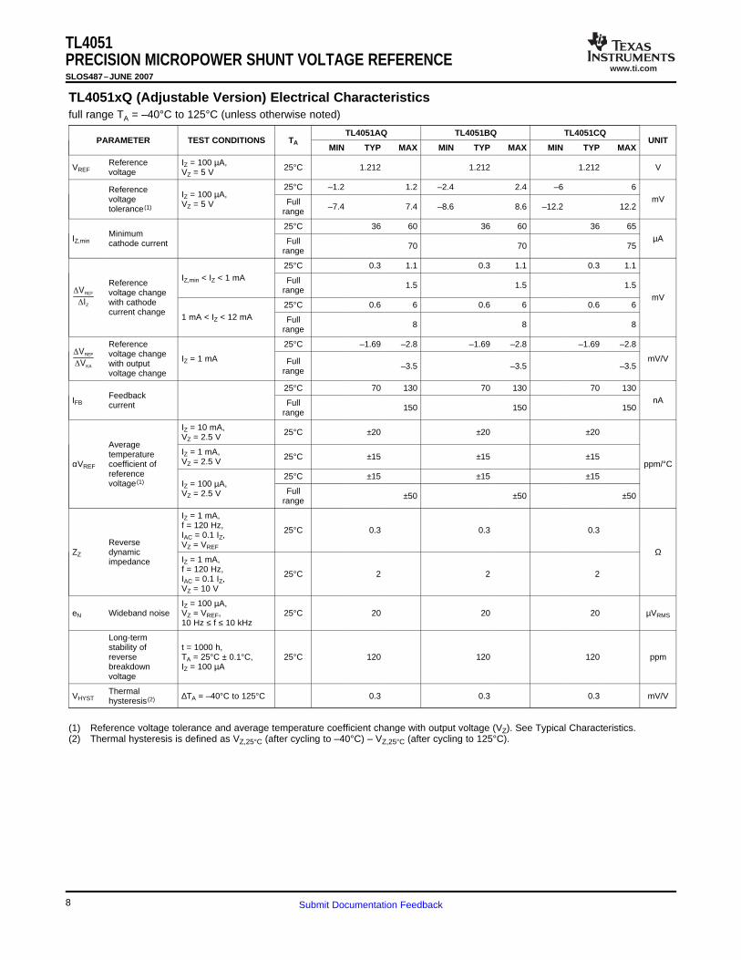
TL4051xQ (Adjustable Version) Electrical Characteristics
DVREF
DIZ
DVREF
DVKA
TL4051PRECISION MICROPOWER SHUNT VOLTAGE REFERENCESLOS487–JUNE 2007
full range TA = –40°C to 125°C (unless otherwise noted)
TL4051AQ TL4051BQ TL4051CQPARAMETER TEST CONDITIONS TA UNIT
MIN TYP MAX MIN TYP MAX MIN TYP MAX
Reference IZ = 100 µA,VREF 25°C 1.212 1.212 1.212 Vvoltage VZ = 5 V
25°C –1.2 1.2 –2.4 2.4 –6 6Reference IZ = 100 µA,voltage mVFullVZ = 5 V –7.4 7.4 –8.6 8.6 –12.2 12.2tolerance (1) range
25°C 36 60 36 60 36 65MinimumIZ,min µAFullcathode current 70 70 75range
25°C 0.3 1.1 0.3 1.1 0.3 1.1IZ,min < IZ < 1 mA FullReference 1.5 1.5 1.5rangevoltage change mVwith cathode 25°C 0.6 6 0.6 6 0.6 6
current change1 mA < IZ < 12 mA Full 8 8 8range
Reference 25°C –1.69 –2.8 –1.69 –2.8 –1.69 –2.8voltage change IZ = 1 mA mV/VFullwith output –3.5 –3.5 –3.5rangevoltage change
25°C 70 130 70 130 70 130FeedbackIFB nAFullcurrent 150 150 150range
IZ = 10 mA, 25°C ±20 ±20 ±20VZ = 2.5 VAverage
IZ = 1 mA,temperature 25°C ±15 ±15 ±15VZ = 2.5 VαVREF coefficient of ppm/°Creference 25°C ±15 ±15 ±15voltage (1) IZ = 100 µA,
FullVZ = 2.5 V ±50 ±50 ±50range
IZ = 1 mA,f = 120 Hz, 25°C 0.3 0.3 0.3IAC = 0.1 IZ,
Reverse VZ = VREFZZ dynamic Ω
IZ = 1 mA,impedancef = 120 Hz, 25°C 2 2 2IAC = 0.1 IZ,VZ = 10 V
IZ = 100 µA,eN Wideband noise VZ = VREF, 25°C 20 20 20 µVRMS
10 Hz ≤ f ≤ 10 kHz
Long-termstability of t = 1000 h,reverse TA = 25°C ± 0.1°C, 25°C 120 120 120 ppmbreakdown IZ = 100 µAvoltage
ThermalVHYST ∆TA = –40°C to 125°C 0.3 0.3 0.3 mV/Vhysteresis (2)
(1) Reference voltage tolerance and average temperature coefficient change with output voltage (VZ). See Typical Characteristics.(2) Thermal hysteresis is defined as VZ,25°C (after cycling to –40°C) – VZ,25°C (after cycling to 125°C).
8 Submit Documentation Feedback
www.ti.com
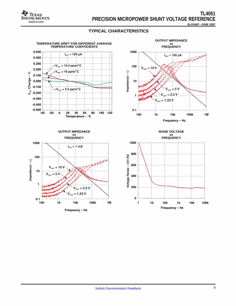
TYPICAL CHARACTERISTICS
-0.500
-0.400
-0.300
-0.200
-0.100
0.000
0.100
0.200
0.300
0.400
0.500
-40 -20 0 20 40 60 80 100 120Temperature – °C
VC
ha
ng
e –
%R
EF
I = 100 µAREF
aV = 5.5 ppm/°CREF
aV = 16 ppm/°CREF
aV = 10.4 ppm/°CREF
0.1
1
10
100
1000
100 1k 10k 100k 1M
Frequency – Hz
Imp
ed
an
ce
–W
I = 150 µAREF
V = 10 VOUT
V = 1.23 VOUT
V = 2.5 VOUT
V = 5 VOUT
0
200
400
600
800
1000
1 10 100 1k 10k 100k
Frequency – Hz
Vo
ltag
e N
ois
e –
nV
/H
zÖ
0.1
1
10
100
1000
100 1k 10k 100k 1M
Frequency – Hz
Imp
ed
an
ce
–W
I = 1 mAREF
V = 10 VOUT
V = 1.23 VOUT
V = 2.5 VOUT
V = 5 VOUT
TL4051PRECISION MICROPOWER SHUNT VOLTAGE REFERENCE
SLOS487–JUNE 2007
OUTPUT IMPEDANCETEMPERATURE DRIFT FOR DIFFERENT AVERAGE vs
TEMPERATURE COEFFICIENTS FREQUENCY
OUTPUT IMPEDANCE NOISE VOLTAGEvs vs
FREQUENCY FREQUENCY
9Submit Documentation Feedback
www.ti.com
0
10
20
30
40
50
60
70
80
90
100
0 2 4 6 8 10
Output Voltage – V
V=
0V
FB
V=
2V
FB
V=
4V
FB
V=
6V
FB
V=
8V
FB
Rev
ers
e C
urr
en
t –
µA
-2
0
2
4
6
8
10
12
14
-5 5 15 25 35 45
Time – µs
Vo
ltag
e –
V
0
20
40
60
80
100
0.0 0.4 0.8 1.2 1.6 2
Reverse Voltage – V
Rev
ers
e C
urr
en
t –
µA
T = -40°CA
T = 125°CA
T = 25°CA
0
0.2
0.4
0.6
0.8
1
1.2
1.4
1.6
0 2 4 6 8 10 12
Output Current – mA
V = V + 5 mVADJ REF
T = –40°CA T = 25°CA
T = 85°CA
T = 125°CA
Ou
tpu
t S
atu
rati
on
–V
TL4051PRECISION MICROPOWER SHUNT VOLTAGE REFERENCESLOS487–JUNE 2007
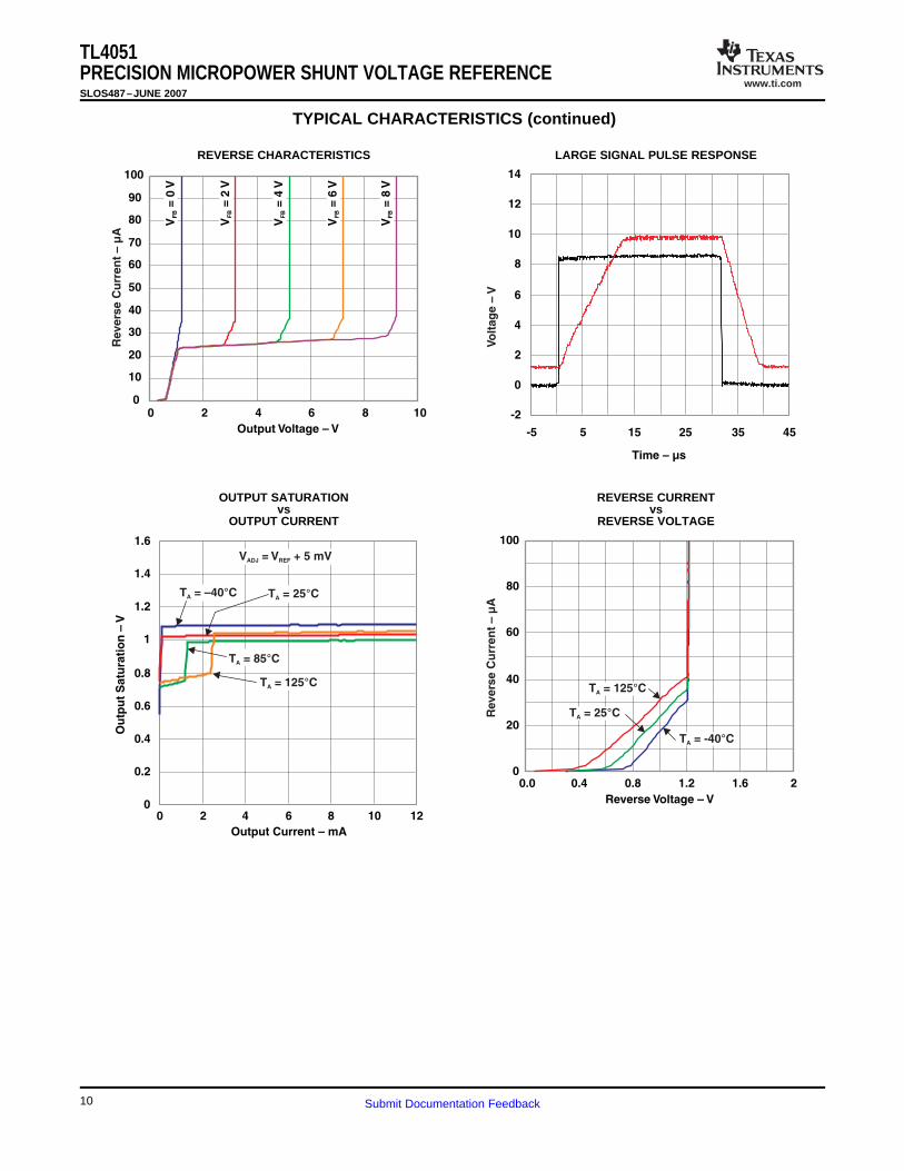
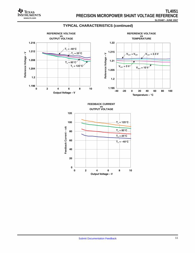
TYPICAL CHARACTERISTICS (continued)
REVERSE CHARACTERISTICS LARGE SIGNAL PULSE RESPONSE
OUTPUT SATURATION REVERSE CURRENTvs vs
OUTPUT CURRENT REVERSE VOLTAGE
10 Submit Documentation Feedback
www.ti.com
1.196
1.2
1.204
1.208
1.212
1.216
0 2 4 6 8 10
Output Voltage – V
Re
fere
nc
eV
olt
ag
e –
V
T = -40°CA
T = 125°CA
T = 85°CA
T = 25°CA
1.195
1.2
1.205
1.21
1.215
1.22
-40 -20 0 20 40 60 80 100
Temperature – °C
Re
fere
nc
eV
olt
ag
e –
V V = VOUT REF V = 2.5 VOUT
V = 5 VOUT V = 10 VOUT
0
20
40
60
80
100
120
0 2 4 6 8 10
Output Voltage – V
T = –40°CA
T = 25°CA
T = 85°CA
T = 125°CA
Fe
ed
ba
ck
Cu
rre
nt
– n
A
TL4051PRECISION MICROPOWER SHUNT VOLTAGE REFERENCE
SLOS487–JUNE 2007
TYPICAL CHARACTERISTICS (continued)
REFERENCE VOLTAGE REFERENCE VOLTAGEvs vs
OUTPUT VOLTAGE TEMPERATURE
FEEDBACK CURRENTvs
OUTPUT VOLTAGE
11Submit Documentation Feedback
www.ti.com
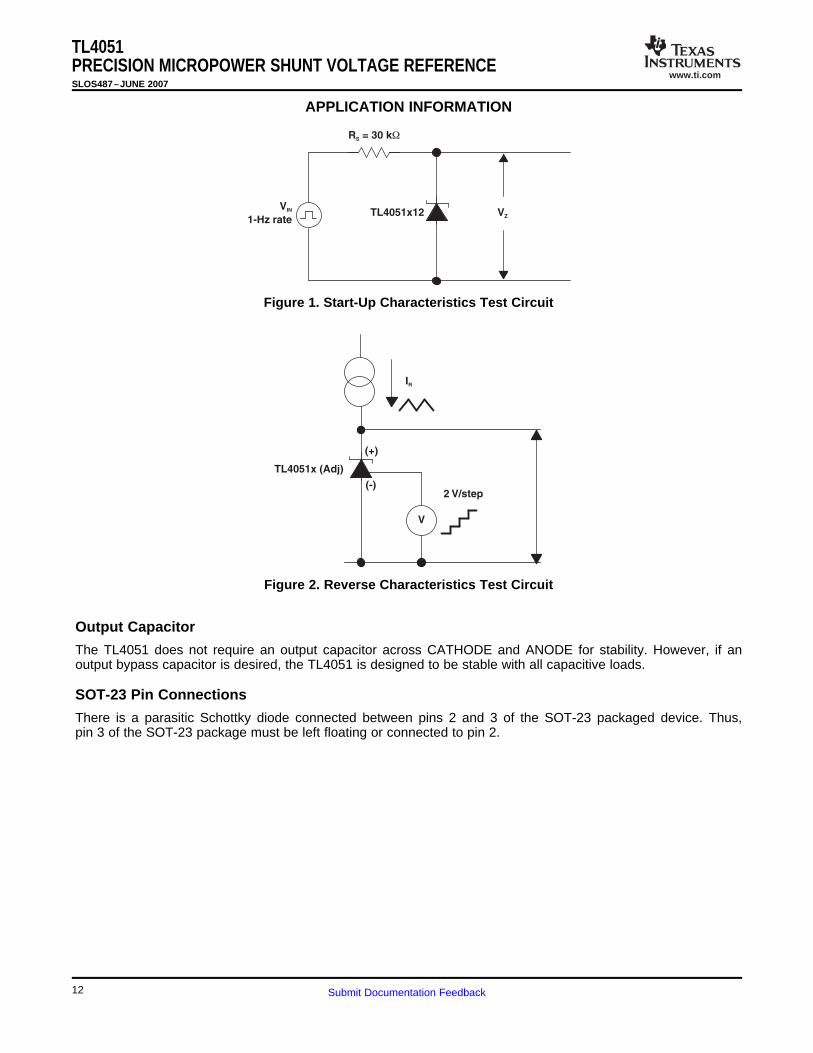
APPLICATION INFORMATION
VZ
TL4051x12
R = 30 kS
W
V
1-Hz rate
IN
IR
(+)
(-)
V
2 V/step
TL4051x (Adj)
Output Capacitor
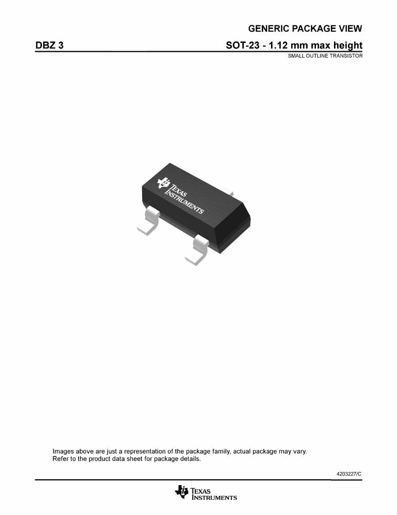
SOT-23 Pin Connections
TL4051PRECISION MICROPOWER SHUNT VOLTAGE REFERENCESLOS487–JUNE 2007
Figure 1. Start-Up Characteristics Test Circuit
Figure 2. Reverse Characteristics Test Circuit
The TL4051 does not require an output capacitor across CATHODE and ANODE for stability. However, if anoutput bypass capacitor is desired, the TL4051 is designed to be stable with all capacitive loads.
There is a parasitic Schottky diode connected between pins 2 and 3 of the SOT-23 packaged device. Thus,pin 3 of the SOT-23 package must be left floating or connected to pin 2.
12 Submit Documentation Feedback
www.ti.com
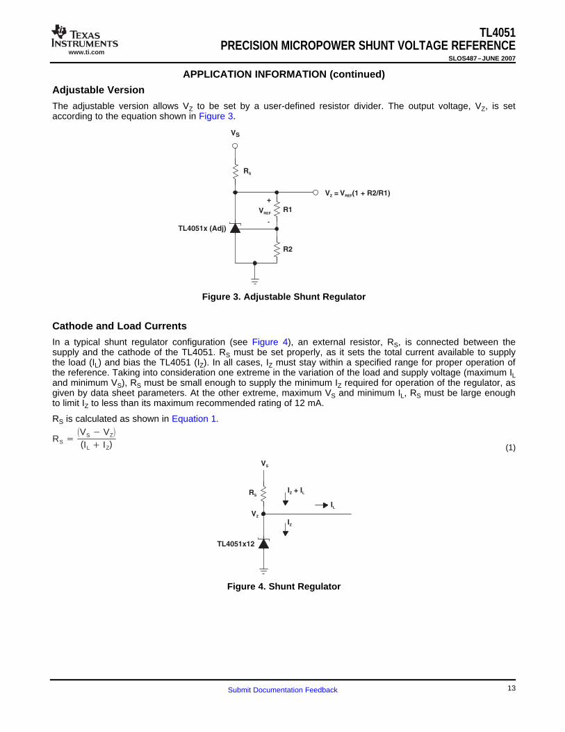
Adjustable Version
RS
TL4051x (Adj)
VS
R1
R2
V = V (1 + R2/R1)Z REF
+
VREF
-
Cathode and Load Currents
RS VS VZ
(IL IZ) (1)
TL4051x12
I + IZ L
IL
IZ
VS
VZ
RS
TL4051PRECISION MICROPOWER SHUNT VOLTAGE REFERENCE
SLOS487–JUNE 2007
APPLICATION INFORMATION (continued)
The adjustable version allows VZ to be set by a user-defined resistor divider. The output voltage, VZ, is setaccording to the equation shown in Figure 3.
Figure 3. Adjustable Shunt Regulator
In a typical shunt regulator configuration (see Figure 4), an external resistor, RS, is connected between thesupply and the cathode of the TL4051. RS must be set properly, as it sets the total current available to supplythe load (IL) and bias the TL4051 (IZ). In all cases, IZ must stay within a specified range for proper operation ofthe reference. Taking into consideration one extreme in the variation of the load and supply voltage (maximum ILand minimum VS), RS must be small enough to supply the minimum IZ required for operation of the regulator, asgiven by data sheet parameters. At the other extreme, maximum VS and minimum IL, RS must be large enoughto limit IZ to less than its maximum recommended rating of 12 mA.
RS is calculated as shown in Equation 1.
Figure 4. Shunt Regulator
13Submit Documentation Feedback
PACKAGE OPTION ADDENDUM
www.ti.com 13-Aug-2021
Addendum-Page 1
PACKAGING INFORMATION
Orderable Device Status(1)
Package Type PackageDrawing
Pins PackageQty
Eco Plan(2)
Lead finish/Ball material
(6)
MSL Peak Temp(3)
Op Temp (°C) Device Marking(4/5)
Samples
TL4051A12IDBZR ACTIVE SOT-23 DBZ 3 3000 RoHS & Green NIPDAU Level-1-260C-UNLIM -40 to 85 TN8U
TL4051A12IDBZRG4 ACTIVE SOT-23 DBZ 3 3000 RoHS & Green NIPDAU Level-1-260C-UNLIM -40 to 85 TN8U
TL4051A12IDBZT ACTIVE SOT-23 DBZ 3 250 RoHS & Green NIPDAU Level-1-260C-UNLIM -40 to 85 TN8U
TL4051A12IDBZTG4 ACTIVE SOT-23 DBZ 3 250 RoHS & Green NIPDAU Level-1-260C-UNLIM -40 to 85 TN8U
TL4051A12QDBZR ACTIVE SOT-23 DBZ 3 3000 RoHS & Green NIPDAU Level-1-260C-UNLIM -40 to 125 TNVU
TL4051A12QDBZT ACTIVE SOT-23 DBZ 3 250 RoHS & Green NIPDAU Level-1-260C-UNLIM -40 to 125 TNVU
TL4051A12QDBZTG4 ACTIVE SOT-23 DBZ 3 250 RoHS & Green NIPDAU Level-1-260C-UNLIM -40 to 125 TNVU
TL4051A12QDCKR ACTIVE SC70 DCK 5 3000 RoHS & Green NIPDAU Level-1-260C-UNLIM -40 to 125 9GU
TL4051AIDBZR ACTIVE SOT-23 DBZ 3 3000 RoHS & Green NIPDAU Level-1-260C-UNLIM -40 to 85 TN2U
TL4051AIDBZT ACTIVE SOT-23 DBZ 3 250 RoHS & Green NIPDAU Level-1-260C-UNLIM -40 to 85 TN2U
TL4051AIDBZTG4 ACTIVE SOT-23 DBZ 3 250 RoHS & Green NIPDAU Level-1-260C-UNLIM -40 to 85 TN2U
TL4051AIDCKR ACTIVE SC70 DCK 5 3000 RoHS & Green NIPDAU Level-1-260C-UNLIM -40 to 85 97U
TL4051AQDBZR ACTIVE SOT-23 DBZ 3 3000 RoHS & Green NIPDAU Level-1-260C-UNLIM -40 to 125 TN5U
TL4051AQDCKR ACTIVE SC70 DCK 5 3000 RoHS & Green NIPDAU Level-1-260C-UNLIM -40 to 125 9AU
TL4051B12IDBZR ACTIVE SOT-23 DBZ 3 3000 RoHS & Green NIPDAU Level-1-260C-UNLIM -40 to 85 (TN93, TN9U)
TL4051B12IDBZT ACTIVE SOT-23 DBZ 3 250 RoHS & Green NIPDAU Level-1-260C-UNLIM -40 to 85 (TN93, TN9U)
TL4051B12QDBZR ACTIVE SOT-23 DBZ 3 3000 RoHS & Green NIPDAU Level-1-260C-UNLIM -40 to 125 (TNW3, TNWU)
TL4051B12QDCKR ACTIVE SC70 DCK 5 3000 RoHS & Green NIPDAU Level-1-260C-UNLIM -40 to 125 9HU
TL4051BIDBZR ACTIVE SOT-23 DBZ 3 3000 RoHS & Green NIPDAU Level-1-260C-UNLIM -40 to 85 TN3U
TL4051BIDBZT ACTIVE SOT-23 DBZ 3 250 RoHS & Green NIPDAU Level-1-260C-UNLIM -40 to 85 TN3U
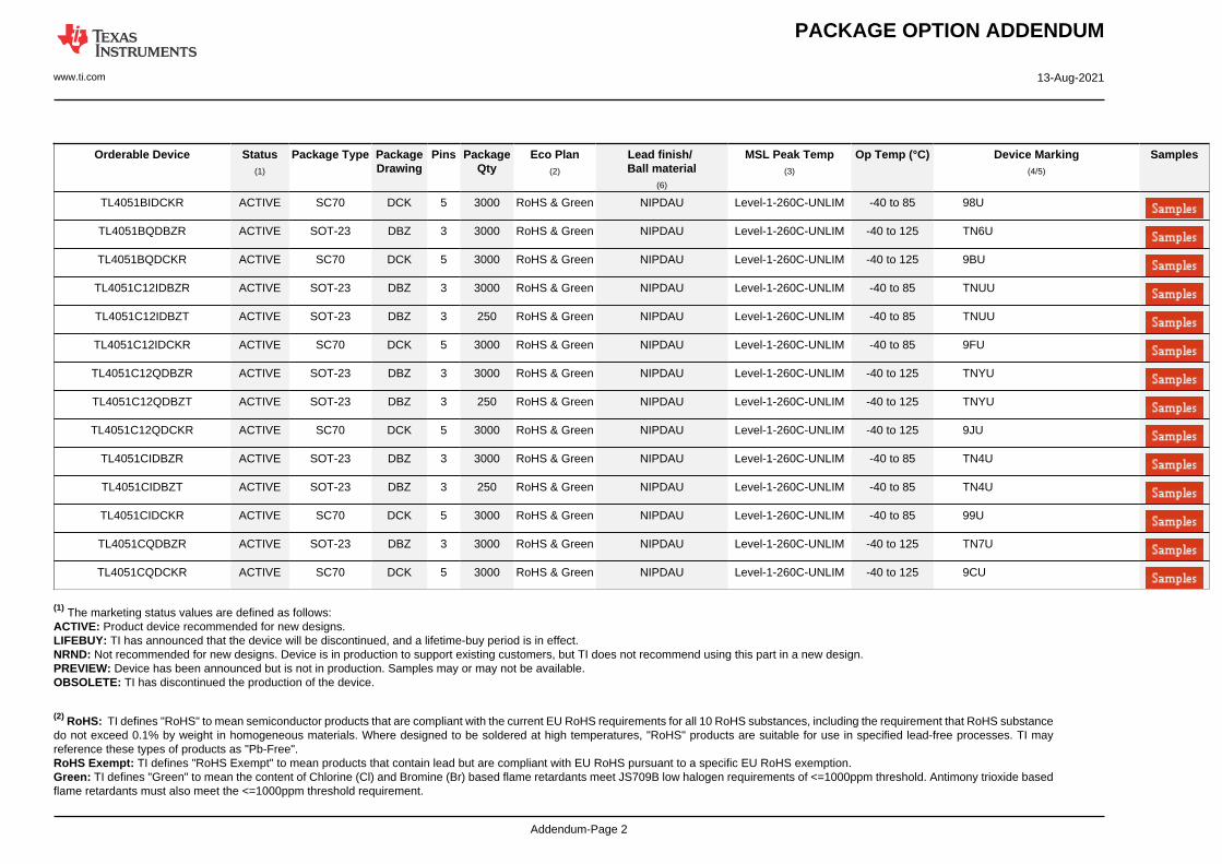
PACKAGE OPTION ADDENDUM
www.ti.com 13-Aug-2021
Addendum-Page 2
Orderable Device Status(1)
Package Type PackageDrawing
Pins PackageQty
Eco Plan(2)
Lead finish/Ball material
(6)
MSL Peak Temp(3)
Op Temp (°C) Device Marking(4/5)
Samples
TL4051BIDCKR ACTIVE SC70 DCK 5 3000 RoHS & Green NIPDAU Level-1-260C-UNLIM -40 to 85 98U
TL4051BQDBZR ACTIVE SOT-23 DBZ 3 3000 RoHS & Green NIPDAU Level-1-260C-UNLIM -40 to 125 TN6U
TL4051BQDCKR ACTIVE SC70 DCK 5 3000 RoHS & Green NIPDAU Level-1-260C-UNLIM -40 to 125 9BU
TL4051C12IDBZR ACTIVE SOT-23 DBZ 3 3000 RoHS & Green NIPDAU Level-1-260C-UNLIM -40 to 85 TNUU
TL4051C12IDBZT ACTIVE SOT-23 DBZ 3 250 RoHS & Green NIPDAU Level-1-260C-UNLIM -40 to 85 TNUU
TL4051C12IDCKR ACTIVE SC70 DCK 5 3000 RoHS & Green NIPDAU Level-1-260C-UNLIM -40 to 85 9FU
TL4051C12QDBZR ACTIVE SOT-23 DBZ 3 3000 RoHS & Green NIPDAU Level-1-260C-UNLIM -40 to 125 TNYU
TL4051C12QDBZT ACTIVE SOT-23 DBZ 3 250 RoHS & Green NIPDAU Level-1-260C-UNLIM -40 to 125 TNYU
TL4051C12QDCKR ACTIVE SC70 DCK 5 3000 RoHS & Green NIPDAU Level-1-260C-UNLIM -40 to 125 9JU
TL4051CIDBZR ACTIVE SOT-23 DBZ 3 3000 RoHS & Green NIPDAU Level-1-260C-UNLIM -40 to 85 TN4U
TL4051CIDBZT ACTIVE SOT-23 DBZ 3 250 RoHS & Green NIPDAU Level-1-260C-UNLIM -40 to 85 TN4U
TL4051CIDCKR ACTIVE SC70 DCK 5 3000 RoHS & Green NIPDAU Level-1-260C-UNLIM -40 to 85 99U
TL4051CQDBZR ACTIVE SOT-23 DBZ 3 3000 RoHS & Green NIPDAU Level-1-260C-UNLIM -40 to 125 TN7U
TL4051CQDCKR ACTIVE SC70 DCK 5 3000 RoHS & Green NIPDAU Level-1-260C-UNLIM -40 to 125 9CU
(1) The marketing status values are defined as follows:ACTIVE: Product device recommended for new designs.LIFEBUY: TI has announced that the device will be discontinued, and a lifetime-buy period is in effect.NRND: Not recommended for new designs. Device is in production to support existing customers, but TI does not recommend using this part in a new design.PREVIEW: Device has been announced but is not in production. Samples may or may not be available.OBSOLETE: TI has discontinued the production of the device.
(2) RoHS: TI defines "RoHS" to mean semiconductor products that are compliant with the current EU RoHS requirements for all 10 RoHS substances, including the requirement that RoHS substancedo not exceed 0.1% by weight in homogeneous materials. Where designed to be soldered at high temperatures, "RoHS" products are suitable for use in specified lead-free processes. TI mayreference these types of products as "Pb-Free".RoHS Exempt: TI defines "RoHS Exempt" to mean products that contain lead but are compliant with EU RoHS pursuant to a specific EU RoHS exemption.Green: TI defines "Green" to mean the content of Chlorine (Cl) and Bromine (Br) based flame retardants meet JS709B low halogen requirements of <=1000ppm threshold. Antimony trioxide basedflame retardants must also meet the <=1000ppm threshold requirement.
PACKAGE OPTION ADDENDUM
www.ti.com 13-Aug-2021
Addendum-Page 3
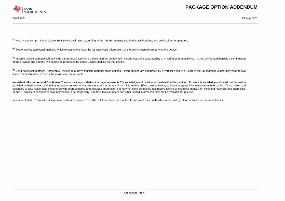
(3) MSL, Peak Temp. - The Moisture Sensitivity Level rating according to the JEDEC industry standard classifications, and peak solder temperature.
(4) There may be additional marking, which relates to the logo, the lot trace code information, or the environmental category on the device.
(5) Multiple Device Markings will be inside parentheses. Only one Device Marking contained in parentheses and separated by a "~" will appear on a device. If a line is indented then it is a continuationof the previous line and the two combined represent the entire Device Marking for that device.
(6) Lead finish/Ball material - Orderable Devices may have multiple material finish options. Finish options are separated by a vertical ruled line. Lead finish/Ball material values may wrap to twolines if the finish value exceeds the maximum column width.
Important Information and Disclaimer:The information provided on this page represents TI's knowledge and belief as of the date that it is provided. TI bases its knowledge and belief on informationprovided by third parties, and makes no representation or warranty as to the accuracy of such information. Efforts are underway to better integrate information from third parties. TI has taken andcontinues to take reasonable steps to provide representative and accurate information but may not have conducted destructive testing or chemical analysis on incoming materials and chemicals.TI and TI suppliers consider certain information to be proprietary, and thus CAS numbers and other limited information may not be available for release.
In no event shall TI's liability arising out of such information exceed the total purchase price of the TI part(s) at issue in this document sold by TI to Customer on an annual basis.
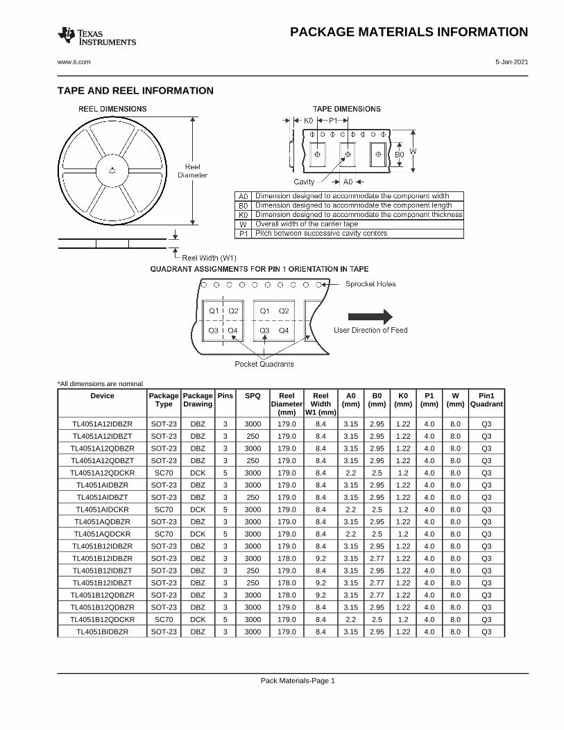
TAPE AND REEL INFORMATION
*All dimensions are nominal
Device PackageType
PackageDrawing
Pins SPQ ReelDiameter
(mm)
ReelWidth
W1 (mm)
A0(mm)
B0(mm)
K0(mm)
P1(mm)
W(mm)
Pin1Quadrant
TL4051A12IDBZR SOT-23 DBZ 3 3000 179.0 8.4 3.15 2.95 1.22 4.0 8.0 Q3
TL4051A12IDBZT SOT-23 DBZ 3 250 179.0 8.4 3.15 2.95 1.22 4.0 8.0 Q3
TL4051A12QDBZR SOT-23 DBZ 3 3000 179.0 8.4 3.15 2.95 1.22 4.0 8.0 Q3
TL4051A12QDBZT SOT-23 DBZ 3 250 179.0 8.4 3.15 2.95 1.22 4.0 8.0 Q3
TL4051A12QDCKR SC70 DCK 5 3000 179.0 8.4 2.2 2.5 1.2 4.0 8.0 Q3
TL4051AIDBZR SOT-23 DBZ 3 3000 179.0 8.4 3.15 2.95 1.22 4.0 8.0 Q3
TL4051AIDBZT SOT-23 DBZ 3 250 179.0 8.4 3.15 2.95 1.22 4.0 8.0 Q3
TL4051AIDCKR SC70 DCK 5 3000 179.0 8.4 2.2 2.5 1.2 4.0 8.0 Q3
TL4051AQDBZR SOT-23 DBZ 3 3000 179.0 8.4 3.15 2.95 1.22 4.0 8.0 Q3
TL4051AQDCKR SC70 DCK 5 3000 179.0 8.4 2.2 2.5 1.2 4.0 8.0 Q3
TL4051B12IDBZR SOT-23 DBZ 3 3000 179.0 8.4 3.15 2.95 1.22 4.0 8.0 Q3
TL4051B12IDBZR SOT-23 DBZ 3 3000 178.0 9.2 3.15 2.77 1.22 4.0 8.0 Q3
TL4051B12IDBZT SOT-23 DBZ 3 250 179.0 8.4 3.15 2.95 1.22 4.0 8.0 Q3
TL4051B12IDBZT SOT-23 DBZ 3 250 178.0 9.2 3.15 2.77 1.22 4.0 8.0 Q3
TL4051B12QDBZR SOT-23 DBZ 3 3000 178.0 9.2 3.15 2.77 1.22 4.0 8.0 Q3
TL4051B12QDBZR SOT-23 DBZ 3 3000 179.0 8.4 3.15 2.95 1.22 4.0 8.0 Q3
TL4051B12QDCKR SC70 DCK 5 3000 179.0 8.4 2.2 2.5 1.2 4.0 8.0 Q3
TL4051BIDBZR SOT-23 DBZ 3 3000 179.0 8.4 3.15 2.95 1.22 4.0 8.0 Q3
PACKAGE MATERIALS INFORMATION
www.ti.com 5-Jan-2021
Pack Materials-Page 1
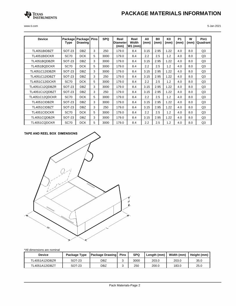
Device PackageType
PackageDrawing
Pins SPQ ReelDiameter
(mm)
ReelWidth
W1 (mm)
A0(mm)
B0(mm)
K0(mm)
P1(mm)
W(mm)
Pin1Quadrant
TL4051BIDBZT SOT-23 DBZ 3 250 179.0 8.4 3.15 2.95 1.22 4.0 8.0 Q3
TL4051BIDCKR SC70 DCK 5 3000 179.0 8.4 2.2 2.5 1.2 4.0 8.0 Q3
TL4051BQDBZR SOT-23 DBZ 3 3000 179.0 8.4 3.15 2.95 1.22 4.0 8.0 Q3
TL4051BQDCKR SC70 DCK 5 3000 179.0 8.4 2.2 2.5 1.2 4.0 8.0 Q3
TL4051C12IDBZR SOT-23 DBZ 3 3000 179.0 8.4 3.15 2.95 1.22 4.0 8.0 Q3
TL4051C12IDBZT SOT-23 DBZ 3 250 179.0 8.4 3.15 2.95 1.22 4.0 8.0 Q3
TL4051C12IDCKR SC70 DCK 5 3000 179.0 8.4 2.2 2.5 1.2 4.0 8.0 Q3
TL4051C12QDBZR SOT-23 DBZ 3 3000 179.0 8.4 3.15 2.95 1.22 4.0 8.0 Q3
TL4051C12QDBZT SOT-23 DBZ 3 250 179.0 8.4 3.15 2.95 1.22 4.0 8.0 Q3
TL4051C12QDCKR SC70 DCK 5 3000 179.0 8.4 2.2 2.5 1.2 4.0 8.0 Q3
TL4051CIDBZR SOT-23 DBZ 3 3000 179.0 8.4 3.15 2.95 1.22 4.0 8.0 Q3
TL4051CIDBZT SOT-23 DBZ 3 250 179.0 8.4 3.15 2.95 1.22 4.0 8.0 Q3
TL4051CIDCKR SC70 DCK 5 3000 179.0 8.4 2.2 2.5 1.2 4.0 8.0 Q3
TL4051CQDBZR SOT-23 DBZ 3 3000 179.0 8.4 3.15 2.95 1.22 4.0 8.0 Q3
TL4051CQDCKR SC70 DCK 5 3000 179.0 8.4 2.2 2.5 1.2 4.0 8.0 Q3
*All dimensions are nominal
Device Package Type Package Drawing Pins SPQ Length (mm) Width (mm) Height (mm)
TL4051A12IDBZR SOT-23 DBZ 3 3000 203.0 203.0 35.0
TL4051A12IDBZT SOT-23 DBZ 3 250 200.0 183.0 25.0
PACKAGE MATERIALS INFORMATION
www.ti.com 5-Jan-2021
Pack Materials-Page 2
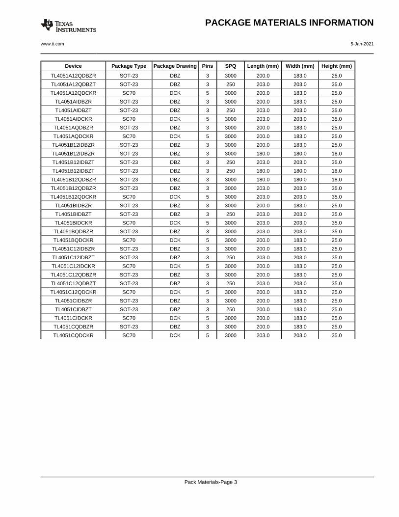
Device Package Type Package Drawing Pins SPQ Length (mm) Width (mm) Height (mm)
TL4051A12QDBZR SOT-23 DBZ 3 3000 200.0 183.0 25.0
TL4051A12QDBZT SOT-23 DBZ 3 250 203.0 203.0 35.0
TL4051A12QDCKR SC70 DCK 5 3000 200.0 183.0 25.0
TL4051AIDBZR SOT-23 DBZ 3 3000 200.0 183.0 25.0
TL4051AIDBZT SOT-23 DBZ 3 250 203.0 203.0 35.0
TL4051AIDCKR SC70 DCK 5 3000 203.0 203.0 35.0
TL4051AQDBZR SOT-23 DBZ 3 3000 200.0 183.0 25.0
TL4051AQDCKR SC70 DCK 5 3000 200.0 183.0 25.0
TL4051B12IDBZR SOT-23 DBZ 3 3000 200.0 183.0 25.0
TL4051B12IDBZR SOT-23 DBZ 3 3000 180.0 180.0 18.0
TL4051B12IDBZT SOT-23 DBZ 3 250 203.0 203.0 35.0
TL4051B12IDBZT SOT-23 DBZ 3 250 180.0 180.0 18.0
TL4051B12QDBZR SOT-23 DBZ 3 3000 180.0 180.0 18.0
TL4051B12QDBZR SOT-23 DBZ 3 3000 203.0 203.0 35.0
TL4051B12QDCKR SC70 DCK 5 3000 203.0 203.0 35.0
TL4051BIDBZR SOT-23 DBZ 3 3000 200.0 183.0 25.0
TL4051BIDBZT SOT-23 DBZ 3 250 203.0 203.0 35.0
TL4051BIDCKR SC70 DCK 5 3000 203.0 203.0 35.0
TL4051BQDBZR SOT-23 DBZ 3 3000 203.0 203.0 35.0
TL4051BQDCKR SC70 DCK 5 3000 200.0 183.0 25.0
TL4051C12IDBZR SOT-23 DBZ 3 3000 200.0 183.0 25.0
TL4051C12IDBZT SOT-23 DBZ 3 250 203.0 203.0 35.0
TL4051C12IDCKR SC70 DCK 5 3000 200.0 183.0 25.0
TL4051C12QDBZR SOT-23 DBZ 3 3000 200.0 183.0 25.0
TL4051C12QDBZT SOT-23 DBZ 3 250 203.0 203.0 35.0
TL4051C12QDCKR SC70 DCK 5 3000 200.0 183.0 25.0
TL4051CIDBZR SOT-23 DBZ 3 3000 200.0 183.0 25.0
TL4051CIDBZT SOT-23 DBZ 3 250 200.0 183.0 25.0
TL4051CIDCKR SC70 DCK 5 3000 200.0 183.0 25.0
TL4051CQDBZR SOT-23 DBZ 3 3000 200.0 183.0 25.0
TL4051CQDCKR SC70 DCK 5 3000 203.0 203.0 35.0
PACKAGE MATERIALS INFORMATION
www.ti.com 5-Jan-2021
Pack Materials-Page 3
4203227/C
www.ti.com
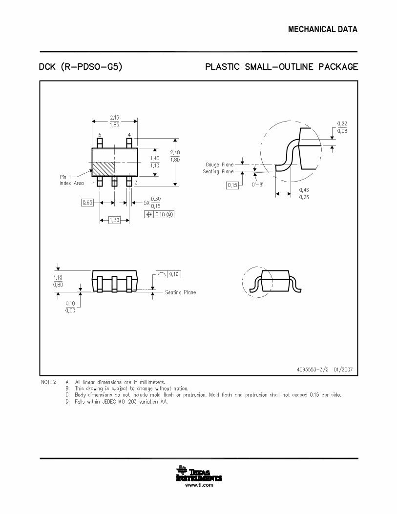
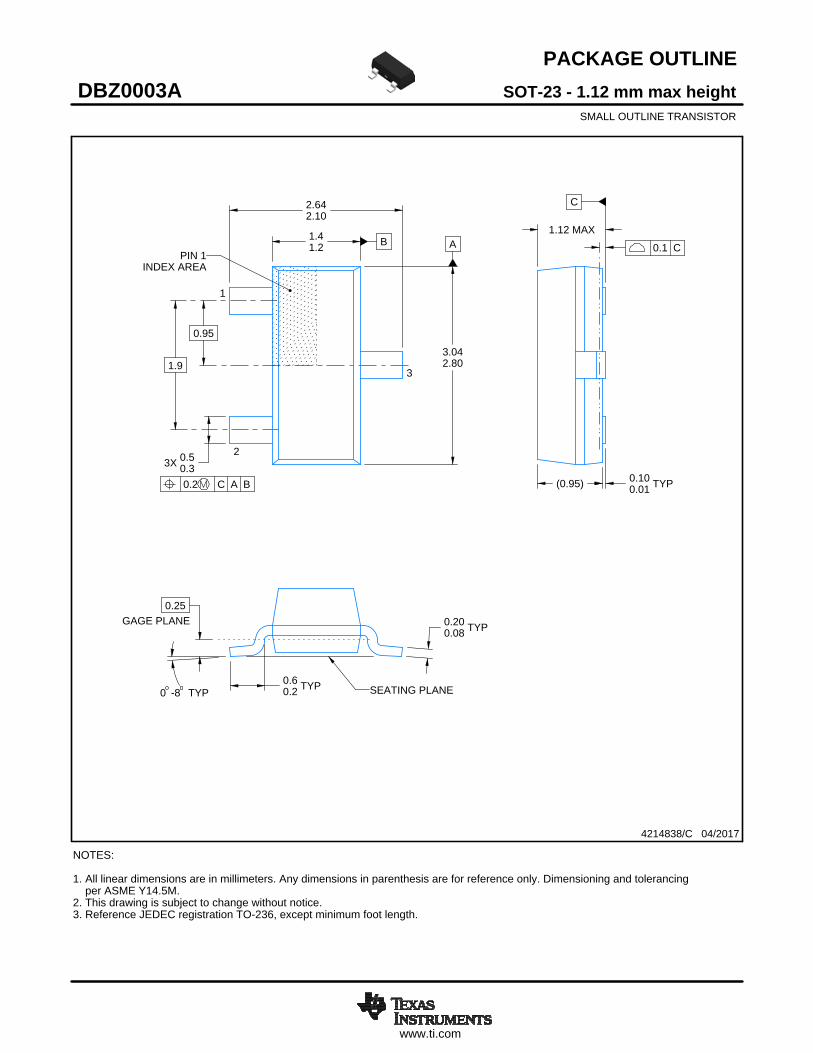
PACKAGE OUTLINE
C
TYP0.200.08
0.25
2.642.10
1.12 MAX
TYP0.100.01
3X 0.50.3
TYP0.60.2
1.9
0.95
TYP-80
A
3.042.80
B1.41.2
(0.95)
SOT-23 - 1.12 mm max heightDBZ0003ASMALL OUTLINE TRANSISTOR
4214838/C 04/2017
NOTES: 1. All linear dimensions are in millimeters. Any dimensions in parenthesis are for reference only. Dimensioning and tolerancing per ASME Y14.5M.2. This drawing is subject to change without notice.3. Reference JEDEC registration TO-236, except minimum foot length.
0.2 C A B
1
3
2
INDEX AREAPIN 1
GAGE PLANE
SEATING PLANE
0.1 C
SCALE 4.000
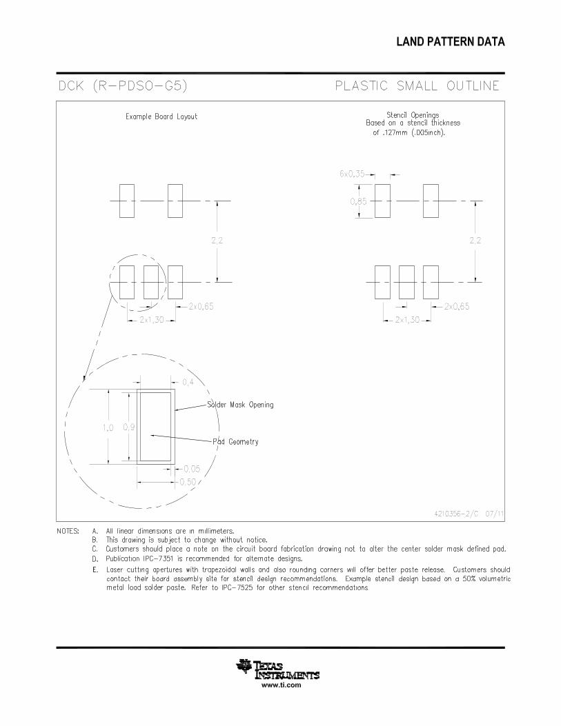
www.ti.com
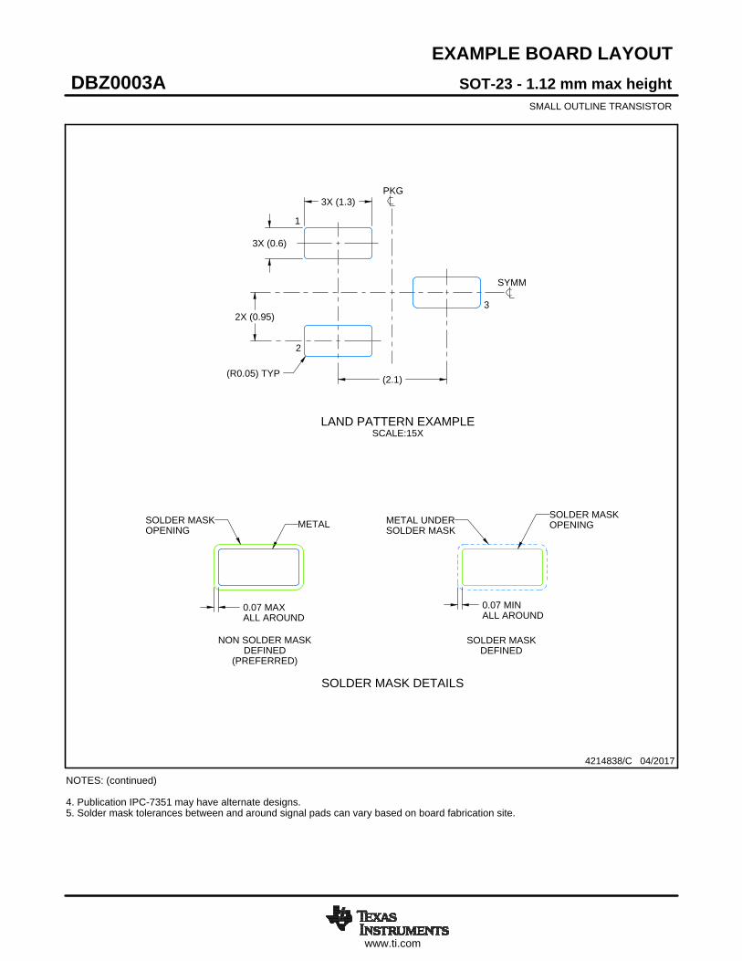
EXAMPLE BOARD LAYOUT
0.07 MAXALL AROUND
0.07 MINALL AROUND
3X (1.3)
3X (0.6)
(2.1)
2X (0.95)
(R0.05) TYP
4214838/C 04/2017
SOT-23 - 1.12 mm max heightDBZ0003ASMALL OUTLINE TRANSISTOR
NOTES: (continued) 4. Publication IPC-7351 may have alternate designs. 5. Solder mask tolerances between and around signal pads can vary based on board fabrication site.
SYMM
LAND PATTERN EXAMPLESCALE:15X
PKG
1
3
2
SOLDER MASKOPENINGMETAL UNDER
SOLDER MASK
SOLDER MASKDEFINED
METALSOLDER MASKOPENING
NON SOLDER MASKDEFINED
(PREFERRED)
SOLDER MASK DETAILS
www.ti.com
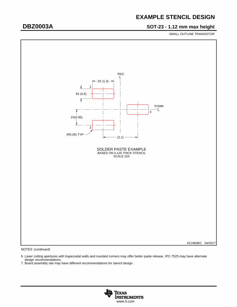
EXAMPLE STENCIL DESIGN
(2.1)
2X(0.95)
3X (1.3)
3X (0.6)
(R0.05) TYP
SOT-23 - 1.12 mm max heightDBZ0003ASMALL OUTLINE TRANSISTOR
4214838/C 04/2017
NOTES: (continued) 6. Laser cutting apertures with trapezoidal walls and rounded corners may offer better paste release. IPC-7525 may have alternate design recommendations. 7. Board assembly site may have different recommendations for stencil design.
SOLDER PASTE EXAMPLEBASED ON 0.125 THICK STENCIL
SCALE:15X
SYMM
PKG
1
3
2

IMPORTANT NOTICE AND DISCLAIMERTI PROVIDES TECHNICAL AND RELIABILITY DATA (INCLUDING DATASHEETS), DESIGN RESOURCES (INCLUDING REFERENCEDESIGNS), APPLICATION OR OTHER DESIGN ADVICE, WEB TOOLS, SAFETY INFORMATION, AND OTHER RESOURCES “AS IS”AND WITH ALL FAULTS, AND DISCLAIMS ALL WARRANTIES, EXPRESS AND IMPLIED, INCLUDING WITHOUT LIMITATION ANYIMPLIED WARRANTIES OF MERCHANTABILITY, FITNESS FOR A PARTICULAR PURPOSE OR NON-INFRINGEMENT OF THIRDPARTY INTELLECTUAL PROPERTY RIGHTS.These resources are intended for skilled developers designing with TI products. You are solely responsible for (1) selecting the appropriateTI products for your application, (2) designing, validating and testing your application, and (3) ensuring your application meets applicablestandards, and any other safety, security, or other requirements. These resources are subject to change without notice. TI grants youpermission to use these resources only for development of an application that uses the TI products described in the resource. Otherreproduction and display of these resources is prohibited. No license is granted to any other TI intellectual property right or to any third partyintellectual property right. TI disclaims responsibility for, and you will fully indemnify TI and its representatives against, any claims, damages,costs, losses, and liabilities arising out of your use of these resources.TI’s products are provided subject to TI’s Terms of Sale (https:www.ti.com/legal/termsofsale.html) or other applicable terms available eitheron ti.com or provided in conjunction with such TI products. TI’s provision of these resources does not expand or otherwise alter TI’sapplicable warranties or warranty disclaimers for TI products.IMPORTANT NOTICE
Mailing Address: Texas Instruments, Post Office Box 655303, Dallas, Texas 75265Copyright © 2021, Texas Instruments Incorporated