Embed Size (px)
Citation preview
CSL316: Digital Hardware Design
Computer Science & Engineering Department I.I.T. Delhi
Copies of old Lecture Transparencies Instructor: M. Balakrishnan
S.No. Topic No. of Slides No. of Lectures 1. Introduction 20 2 2. Review of Combinational 56 5
Circuit Design
3. Sequential Circuits 83 7 4. Asynchronous Circuits 25 3 5. Microprogrammed Control 60 5 6. Introduction to VHDL 34 3 7. Testing of Digital Circuits 58 5 8. Advanced Topics 37 4
1
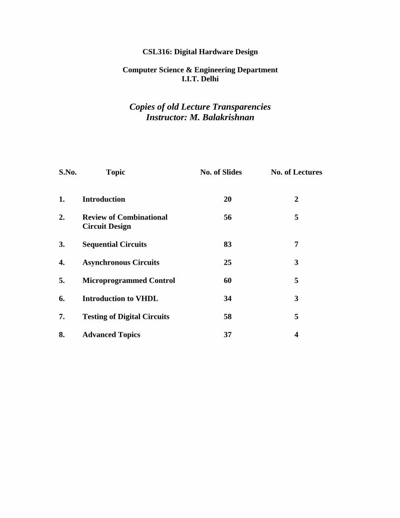
Chapter 1: Introduction 1
Digital Hardware Design
M. BalakrishnanDept. of Comp. Sci. & Engg.
I.I.T. Delhi
Chapter 1: Introduction 2
Introduction
• What are digital systems ?
• Applications
• Design steps
Chapter 1: Introduction 3
Representation
• Discrete time for signals– Clock for synchronous systems
• Quantized for all types of data– Binary number representation
Chapter 1: Introduction 4
Advantages Over Analog
• Programmability• Predictable accuracy• Maintainability
Though Analog systems are still used at very high frequency
Chapter 1: Introduction 5
Applications
Nature of Application Time Constraints• Real time computing Hard
• Interactive computing Soft
• Off-line computing -
Chapter 1: Introduction 6
Digital System Examples
• Consumer electronics• Radar & sonar processing• Control systems• General computing• Mobile computing
2
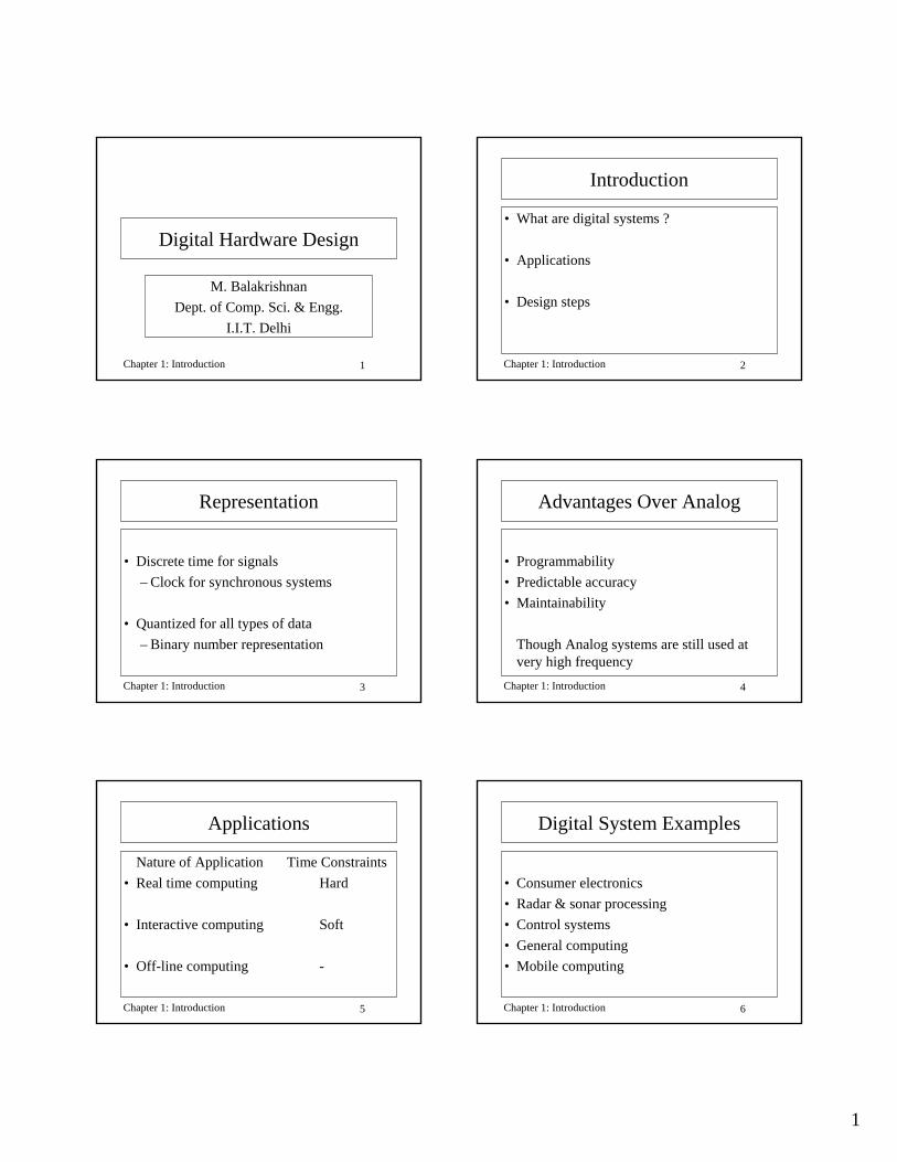
Chapter 1: Introduction 7
System Design Steps
Verification
Verification
Specification
Circuit
Synthesis
Chapter 1: Introduction 8
Specification Language
• English(/any natural language)– Ambiguous and not suitable for
processing by machine• Hardware description language
– Machine simulatable/executable but difficult to write
Chapter 1: Introduction 9
Synthesis Methodologies
Synthesis refers to the transformation of specification (behavior) torealization (structure)
• Manual– Ad-hoc– Procedural
• Automated
Chapter 1: Introduction 10
Digital Systems DevelopmentTechnology & Issues
M. BalakrishnanDept. of Comp. Sci. & Engg.
I.I.T. Delhi
Chapter 1: Introduction 11
Development of Digital Systems
• SSI: Small Scale Integration• MSI: Medium Scale Integration• LSI: Large Scale Integration• VLSI: Very Large Scale Integration• SOC: System on Chip
Chapter 1: Introduction 12
Driving Factor: Semiconductor Technology
• Key parameter (feature size)– Distance between two conducting lines– Size of the transistor50.0 micron to 0.12 micron
• Driving Device: Memory
3
Chapter 1: Introduction 13
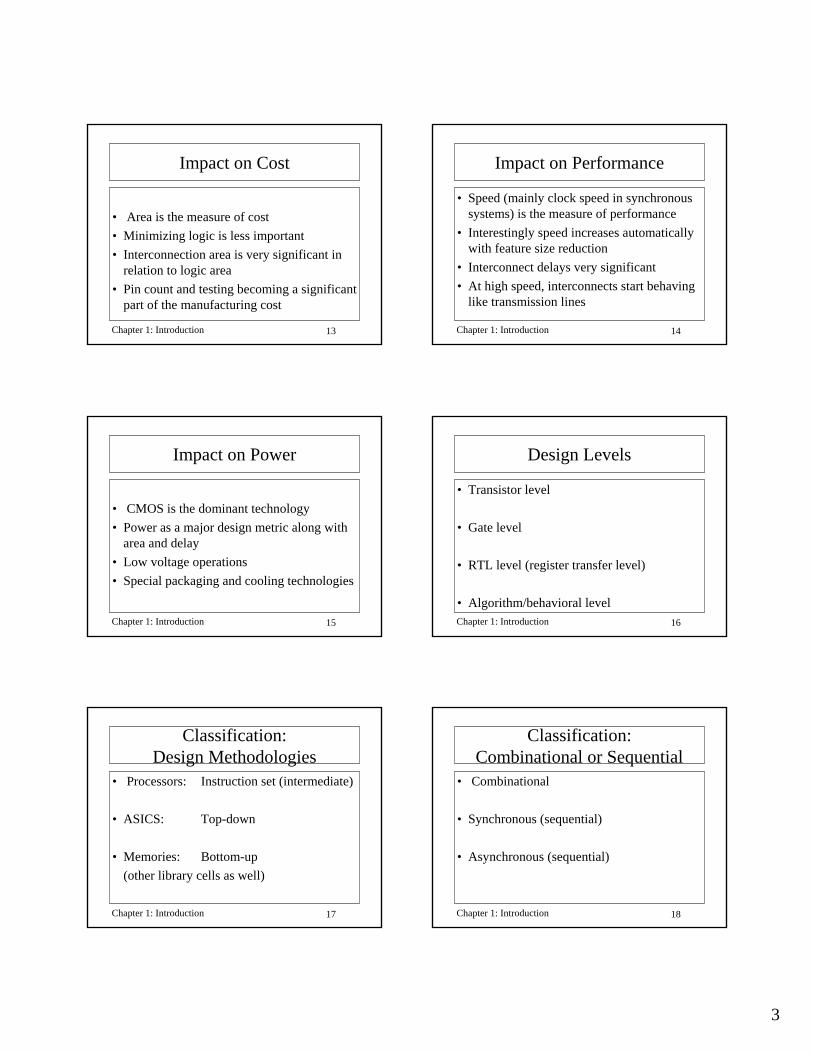
Impact on Cost
• Area is the measure of cost• Minimizing logic is less important• Interconnection area is very significant in
relation to logic area• Pin count and testing becoming a significant
part of the manufacturing cost
Chapter 1: Introduction 14
Impact on Performance
• Speed (mainly clock speed in synchronous systems) is the measure of performance
• Interestingly speed increases automatically with feature size reduction
• Interconnect delays very significant• At high speed, interconnects start behaving
like transmission lines
Chapter 1: Introduction 15
Impact on Power
• CMOS is the dominant technology• Power as a major design metric along with
area and delay • Low voltage operations• Special packaging and cooling technologies
Chapter 1: Introduction 16
Design Levels
• Transistor level
• Gate level
• RTL level (register transfer level)
• Algorithm/behavioral level
Chapter 1: Introduction 17
Classification: Design Methodologies
• Processors: Instruction set (intermediate)
• ASICS: Top-down
• Memories: Bottom-up(other library cells as well)
Chapter 1: Introduction 18
Classification: Combinational or Sequential
• Combinational
• Synchronous (sequential)
• Asynchronous (sequential)
4
Chapter 1: Introduction 19
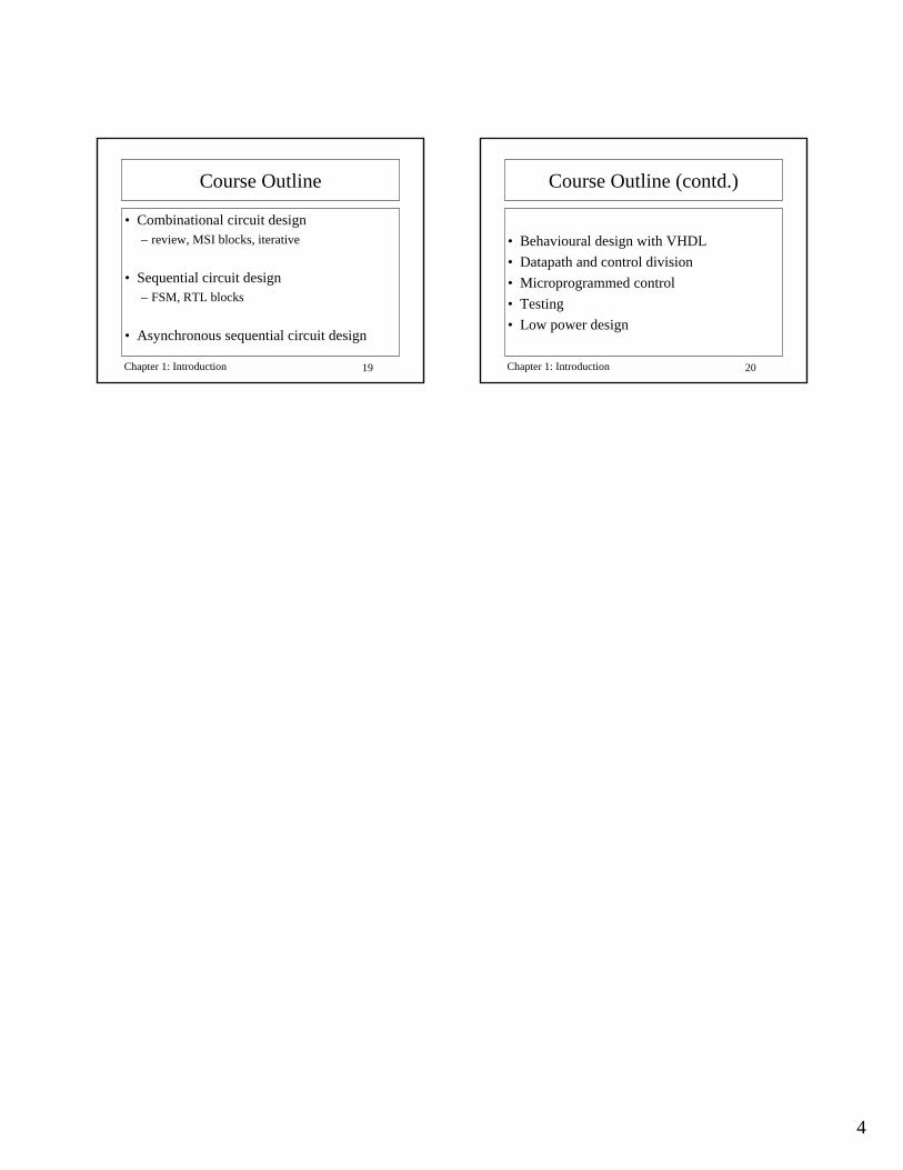
Course Outline
• Combinational circuit design– review, MSI blocks, iterative
• Sequential circuit design– FSM, RTL blocks
• Asynchronous sequential circuit design
Chapter 1: Introduction 20
Course Outline (contd.)
• Behavioural design with VHDL• Datapath and control division• Microprogrammed control• Testing• Low power design
1
Chapter 2: Combinational Circuits 1
Review of Combinational Circuit Design
M. BalakrishnanDept. of Comp. Sci. & Engg.
I.I.T. Delhi
Chapter 2: Combinational Circuits 2
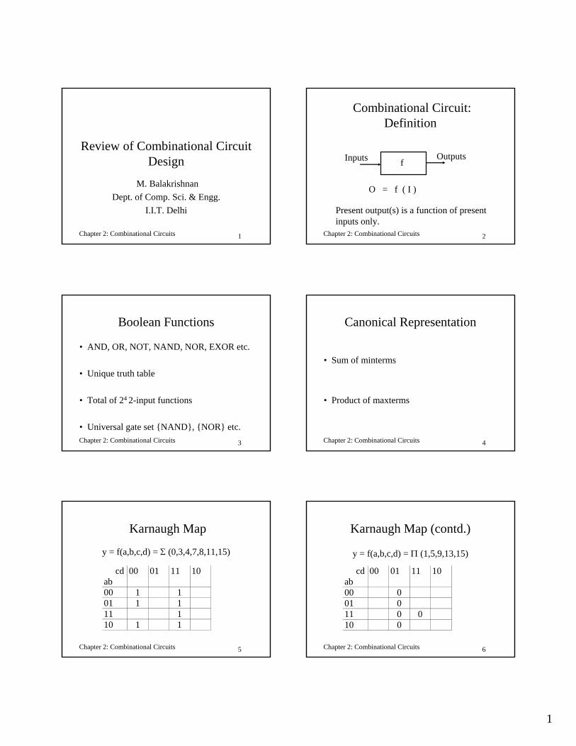
Combinational Circuit: Definition
Inputs Outputsf
O = f ( I )
Present output(s) is a function of presentinputs only.
Chapter 2: Combinational Circuits 3
Boolean Functions
• AND, OR, NOT, NAND, NOR, EXOR etc.
• Unique truth table
• Total of 24 2-input functions
• Universal gate set {NAND}, {NOR} etc.Chapter 2: Combinational Circuits 4
Canonical Representation
• Sum of minterms
• Product of maxterms
Chapter 2: Combinational Circuits 5
Karnaugh Map
y = f(a,b,c,d) = Σ (0,3,4,7,8,11,15)
cdab
00 01 11 10
00 1 101 1 111 110 1 1
Chapter 2: Combinational Circuits 6
Karnaugh Map (contd.)
y = f(a,b,c,d) = Π (1,5,9,13,15)
cdab
00 01 11 10
00 001 011 0 010 0
2
Chapter 2: Combinational Circuits 7
Duality
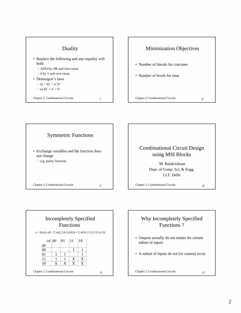
• Replace the following and any equality will hold– AND by OR and vice-versa– 0 by 1 and vice-versa
• Demorgon’s laws– (a + b)’ = a’.b’– (a.b)’ = a’ + b’
Chapter 2: Combinational Circuits 8
Minimization Objectives
• Number of literals for cost/area
• Number of levels for time
Chapter 2: Combinational Circuits 9
Symmetric Functions
• Exchange variables and the function does not change– e.g. parity function
Chapter 2: Combinational Circuits 10
Combinational Circuit Designusing MSI Blocks
M. BalakrishnanDept. of Comp. Sci. & Engg.
I.I.T. Delhi
Chapter 2: Combinational Circuits 11
Incompletely Specified Functions
cdab
00 01 11 10
00 1 101 1 1 111 1 1 X X10 X X X X
y = f(a,b,c,d) = Σ m(2,3,4,5,6,8,9) + Σ d(10,11,12,13,14,15)
Chapter 2: Combinational Circuits 12
Why Incompletely Specified Functions ?
• Outputs actually do not matter for certain subset of inputs
• A subset of inputs do not (or cannot) occur
3
Chapter 2: Combinational Circuits 13
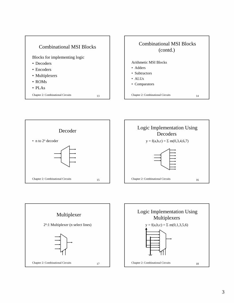
Combinational MSI Blocks
Blocks for implementing logic• Decoders• Encoders• Multiplexers• ROMs• PLAs
Chapter 2: Combinational Circuits 14
Combinational MSI Blocks (contd.)
Arithmetic MSI Blocks• Adders• Subtractors• ALUs• Comparators
Chapter 2: Combinational Circuits 15
Decoder
• n to 2n decoder
Chapter 2: Combinational Circuits 16
Logic Implementation Using Decoders
y = f(a,b,c) = Σ m(0,3,4,6,7)
Chapter 2: Combinational Circuits 17
Multiplexer
2n:1 Multiplexer (n select lines)
Chapter 2: Combinational Circuits 18
Logic Implementation Using Multiplexers
y = f(a,b,c) = Σ m(0,1,3,5,6)
4
Chapter 2: Combinational Circuits 19
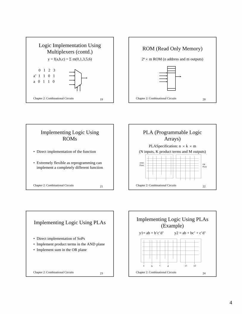
Logic Implementation Using Multiplexers (contd.)y = f(a,b,c) = Σ m(0,1,3,5,6)
0 1 2 3a’ 1 1 0 1a 0 1 1 0
Chapter 2: Combinational Circuits 20
ROM (Read Only Memory)
2n × m ROM (n address and m outputs)
Chapter 2: Combinational Circuits 21
Implementing Logic Using ROMs
• Direct implementation of the function
• Extremely flexible as reprogramming can implement a completely different function
Chapter 2: Combinational Circuits 22
PLA (Programmable Logic Arrays)
PLASpecification: n × k × m (N inputs, K product terms and M outputs)
ANDPlane OR
Plane
Chapter 2: Combinational Circuits 23
Implementing Logic Using PLAs
• Direct implementation of SoPs• Implement product terms in the AND plane• Implement sum in the OR plane
Chapter 2: Combinational Circuits 24
Implementing Logic Using PLAs (Example)
y1= ab + b’c’d’ y2 = ab + bc’ + c’d’
a b c d y1 y2
5
Chapter 2: Combinational Circuits 25
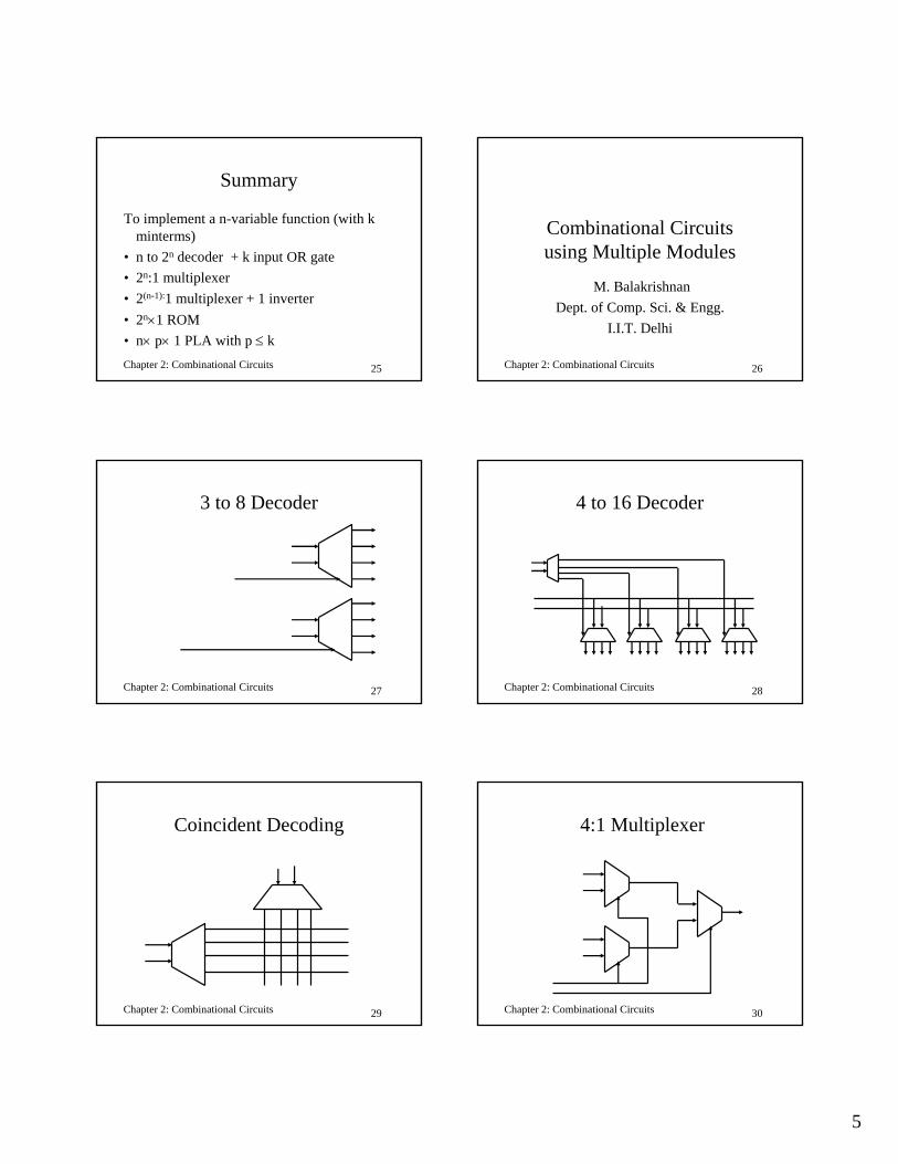
Summary
To implement a n-variable function (with k minterms)
• n to 2n decoder + k input OR gate• 2n:1 multiplexer• 2(n-1):1 multiplexer + 1 inverter• 2n×1 ROM• n× p× 1 PLA with p ≤ k
Chapter 2: Combinational Circuits 26
Combinational Circuitsusing Multiple Modules
M. BalakrishnanDept. of Comp. Sci. & Engg.
I.I.T. Delhi
Chapter 2: Combinational Circuits 27
3 to 8 Decoder
Chapter 2: Combinational Circuits 28
4 to 16 Decoder
Chapter 2: Combinational Circuits 29
Coincident Decoding
Chapter 2: Combinational Circuits 30
4:1 Multiplexer
6
Chapter 2: Combinational Circuits 31
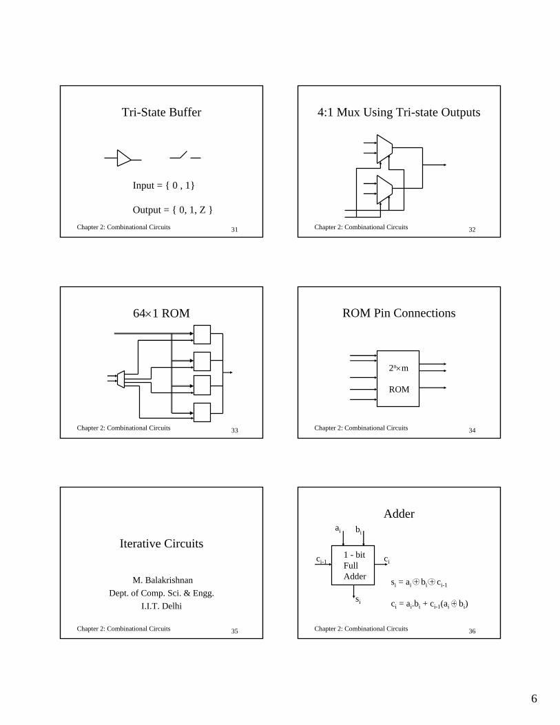
Tri-State Buffer
Input = { 0 , 1}
Output = { 0, 1, Z }Chapter 2: Combinational Circuits 32
4:1 Mux Using Tri-state Outputs
Chapter 2: Combinational Circuits 33
64×1 ROM
Chapter 2: Combinational Circuits 34
ROM Pin Connections
2n×m
ROM
Chapter 2: Combinational Circuits 35
Iterative Circuits
M. BalakrishnanDept. of Comp. Sci. & Engg.
I.I.T. Delhi
Chapter 2: Combinational Circuits 36
Adder
1 - bitFullAdder si = ai + bi + ci-1
ci = ai.bi + ci-1(ai + bi)
ai bi
ci-1
si
ci
7
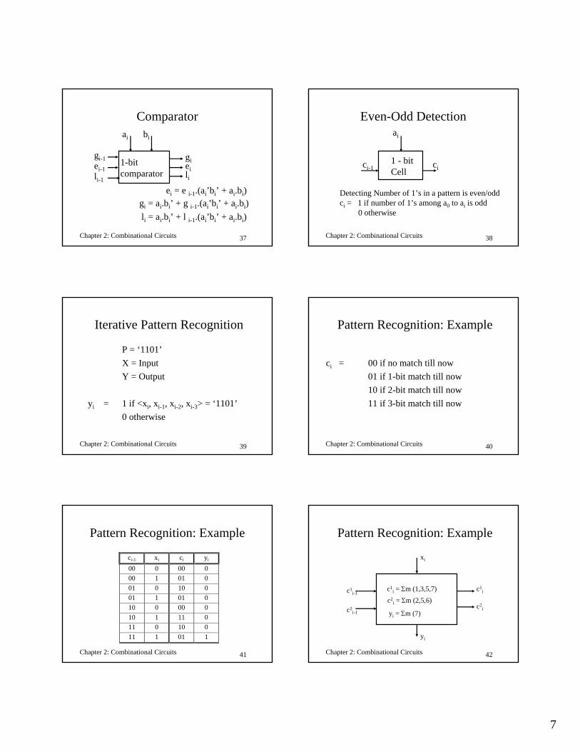
Chapter 2: Combinational Circuits 37
Comparator
1-bitcomparator
bi
li-1li
ei = e i-1.(ai’bi’ + ai.bi)gi = ai.bi’ + g i-1.(ai’bi’ + ai.bi)li = ai.bi’ + l i-1.(ai’bi’ + ai.bi)
ai
ei
giei-1
gi-1
Chapter 2: Combinational Circuits 38
Even-Odd Detection
1 - bitCell
ai
ci-1 ci
Detecting Number of 1’s in a pattern is even/oddci = 1 if number of 1’s among a0 to ai is odd
0 otherwise
Chapter 2: Combinational Circuits 39
Iterative Pattern Recognition
P = ‘1101’X = Input Y = Output
yi = 1 if <xi, xi-1, xi-2, xi-3> = ‘1101’0 otherwise
Chapter 2: Combinational Circuits 40
Pattern Recognition: Example
ci = 00 if no match till now01 if 1-bit match till now10 if 2-bit match till now11 if 3-bit match till now
Chapter 2: Combinational Circuits 41
Pattern Recognition: Example
ci-1 xi ci yi
00 0 00 000 1 01 001 0 10 001 1 01 010 0 00 010 1 11 011 0 10 011 1 01 1
Chapter 2: Combinational Circuits 42
Pattern Recognition: Example
c1i = Σm (1,3,5,7)
c2i = Σm (2,5,6)
yi = Σm (7)
c1i
c2ic2
i-1
c1i-1
xi
yi
8
Chapter 2: Combinational Circuits 43
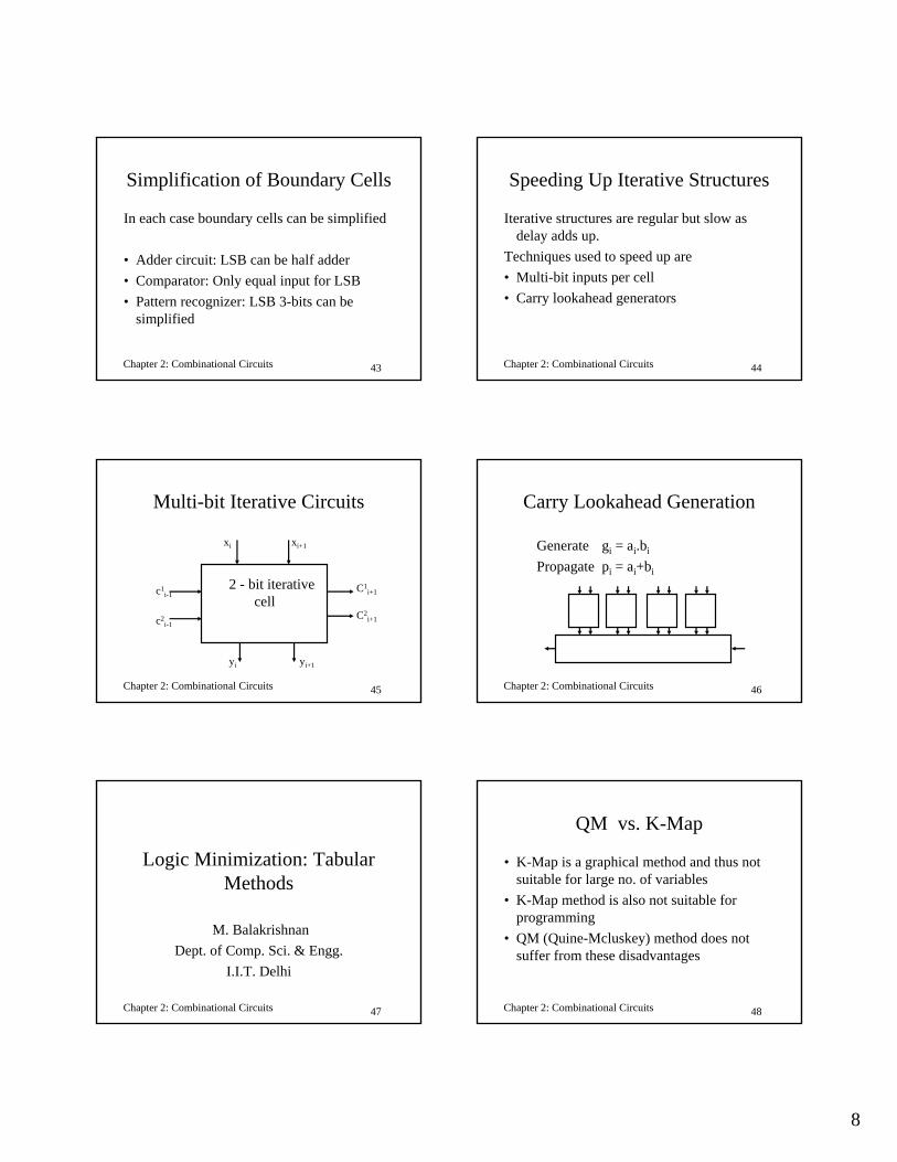
Simplification of Boundary Cells
In each case boundary cells can be simplified
• Adder circuit: LSB can be half adder• Comparator: Only equal input for LSB• Pattern recognizer: LSB 3-bits can be
simplified
Chapter 2: Combinational Circuits 44
Speeding Up Iterative Structures
Iterative structures are regular but slow as delay adds up.
Techniques used to speed up are• Multi-bit inputs per cell• Carry lookahead generators
Chapter 2: Combinational Circuits 45
Multi-bit Iterative Circuits
C1i+1
C2i+1c2
i-1
c1i-1
2 - bit iterativecell
yi yi+1
xi+1xi
Chapter 2: Combinational Circuits 46
Carry Lookahead Generation
Generate gi = ai.bi
Propagate pi = ai+bi
Chapter 2: Combinational Circuits 47
Logic Minimization: Tabular Methods
M. BalakrishnanDept. of Comp. Sci. & Engg.
I.I.T. Delhi
Chapter 2: Combinational Circuits 48
QM vs. K-Map
• K-Map is a graphical method and thus not suitable for large no. of variables
• K-Map method is also not suitable for programming
• QM (Quine-Mcluskey) method does not suffer from these disadvantages
9
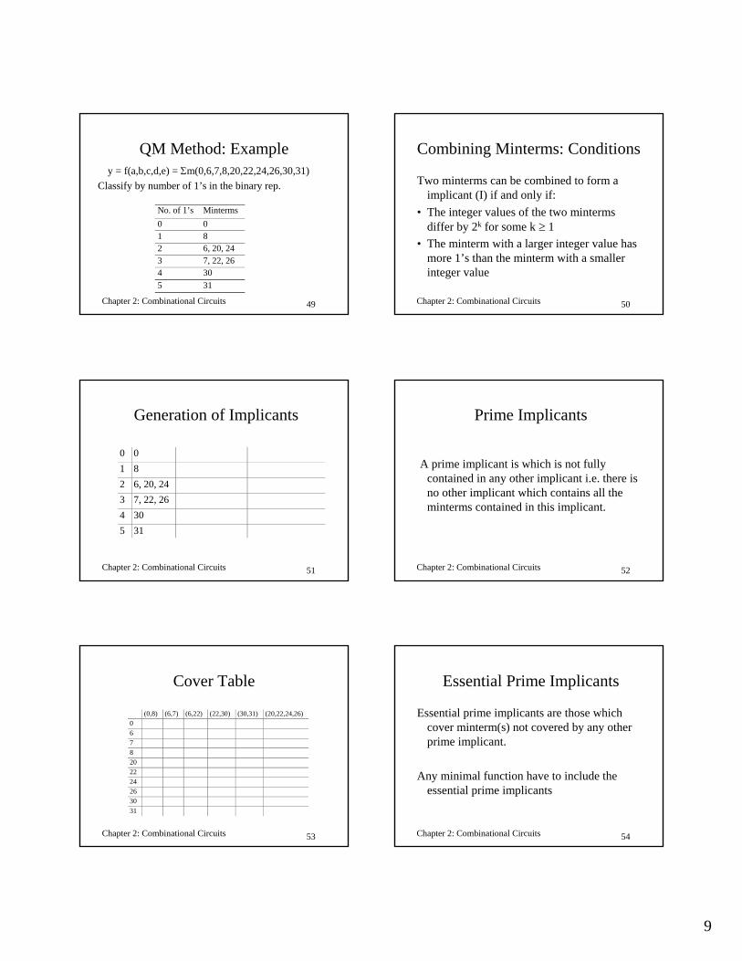
Chapter 2: Combinational Circuits 49
QM Method: Exampley = f(a,b,c,d,e) = Σm(0,6,7,8,20,22,24,26,30,31)
Classify by number of 1’s in the binary rep.
No. of 1’s Minterms0 01 82 6, 20, 243 7, 22, 264 305 31
Chapter 2: Combinational Circuits 50
Combining Minterms: Conditions
Two minterms can be combined to form a implicant (I) if and only if:
• The integer values of the two minterms differ by 2k for some k ≥ 1
• The minterm with a larger integer value has more 1’s than the minterm with a smaller integer value
Chapter 2: Combinational Circuits 51
Generation of Implicants
0 01 82 6, 20, 243 7, 22, 264 305 31
Chapter 2: Combinational Circuits 52
Prime Implicants
A prime implicant is which is not fully contained in any other implicant i.e. there is no other implicant which contains all the minterms contained in this implicant.
Chapter 2: Combinational Circuits 53
Cover Table
(0,8) (6,7) (6,22) (22,30) (30,31) (20,22,24,26)0678202224263031
Chapter 2: Combinational Circuits 54
Essential Prime Implicants
Essential prime implicants are those which cover minterm(s) not covered by any other prime implicant.
Any minimal function have to include the essential prime implicants
10
Chapter 2: Combinational Circuits 55
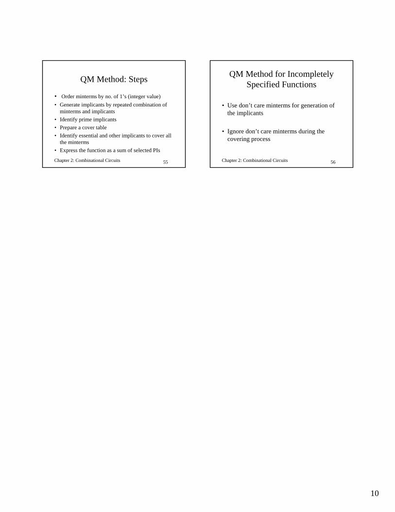
QM Method: Steps
• Order minterms by no. of 1’s (integer value)• Generate implicants by repeated combination of
minterms and implicants• Identify prime implicants• Prepare a cover table• Identify essential and other implicants to cover all
the minterms• Express the function as a sum of selected PIs
Chapter 2: Combinational Circuits 56
QM Method for Incompletely Specified Functions
• Use don’t care minterms for generation of the implicants
• Ignore don’t care minterms during the covering process
1
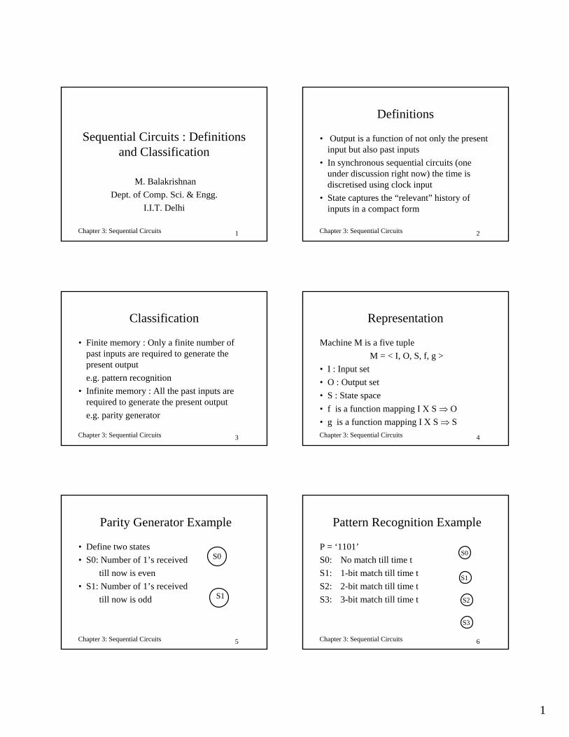
Chapter 3: Sequential Circuits 1
Sequential Circuits : Definitions and Classification
M. BalakrishnanDept. of Comp. Sci. & Engg.
I.I.T. Delhi
Chapter 3: Sequential Circuits 2
Definitions
• Output is a function of not only the present input but also past inputs
• In synchronous sequential circuits (one under discussion right now) the time is discretised using clock input
• State captures the “relevant” history of inputs in a compact form
Chapter 3: Sequential Circuits 3
Classification
• Finite memory : Only a finite number of past inputs are required to generate the present output e.g. pattern recognition
• Infinite memory : All the past inputs are required to generate the present output e.g. parity generator
Chapter 3: Sequential Circuits 4
Representation
Machine M is a five tupleM = < I, O, S, f, g >
• I : Input set• O : Output set• S : State space• f is a function mapping I Χ S ⇒ O• g is a function mapping I Χ S ⇒ S
Chapter 3: Sequential Circuits 5
Parity Generator Example
• Define two states• S0: Number of 1’s received
till now is even• S1: Number of 1’s received
till now is odd
S0
S1
Chapter 3: Sequential Circuits 6
Pattern Recognition Example
P = ‘1101’S0: No match till time tS1: 1-bit match till time tS2: 2-bit match till time tS3: 3-bit match till time t
S0
S1
S2
S3
2
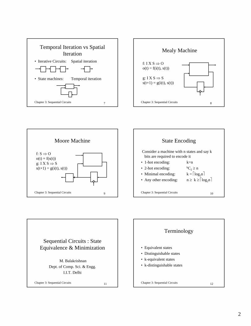
Chapter 3: Sequential Circuits 7
Temporal Iteration vs Spatial Iteration
• Iterative Circuits: Spatial iteration
• State machines: Temporal iteration
Chapter 3: Sequential Circuits 8
Mealy Machine
f: I Χ S ⇒ Oo(t) = f(i(t), s(t))
g: I Χ S ⇒ Ss(t+1) = g(i(t), s(t))
Chapter 3: Sequential Circuits 9
Moore Machine
f: S ⇒ Oo(t) = f(s(t))g: I Χ S ⇒ Ss(t+1) = g(i(t), s(t))
Chapter 3: Sequential Circuits 10
State Encoding
Consider a machine with n states and say k bits are required to encode it
• 1-hot encoding: k=n• 2-hot encoding: kC2 ≥ n• Minimal encoding: k = ⎡log2n⎤• Any other encoding: n ≥ k ≥ ⎡log2n⎤
Chapter 3: Sequential Circuits 11
Sequential Circuits : State Equivalence & Minimization
M. BalakrishnanDept. of Comp. Sci. & Engg.
I.I.T. Delhi
Chapter 3: Sequential Circuits 12
Terminology
• Equivalent states• Distinguishable states• k-equivalent states• k-distinguishable states
3
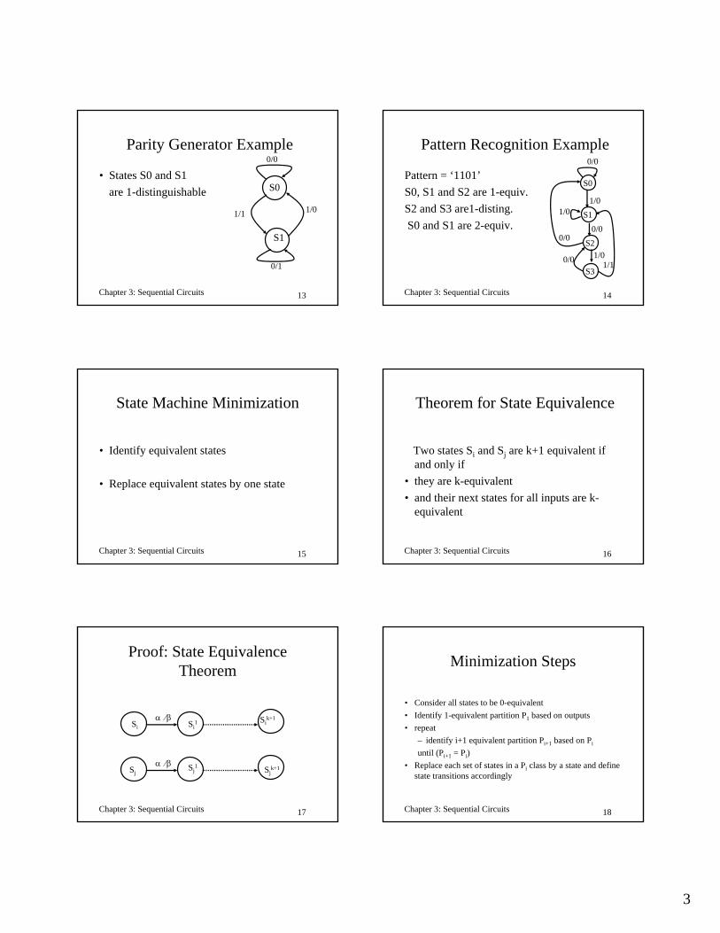
Chapter 3: Sequential Circuits 13
Parity Generator Example
• States S0 and S1are 1-distinguishable S0
S1
0/0
1/1
0/1
1/0
Chapter 3: Sequential Circuits 14
Pattern Recognition Example
Pattern = ‘1101’S0, S1 and S2 are 1-equiv.S2 and S3 are1-disting.S0 and S1 are 2-equiv.
S0
S1
S2
S3
0/0
1/01/0
0/00/0
1/01/10/0
Chapter 3: Sequential Circuits 15
State Machine Minimization
• Identify equivalent states
• Replace equivalent states by one state
Chapter 3: Sequential Circuits 16
Theorem for State Equivalence
Two states Si and Sj are k+1 equivalent if and only if
• they are k-equivalent• and their next states for all inputs are k-
equivalent
Chapter 3: Sequential Circuits 17
Proof: State Equivalence Theorem
Si Si1
SjSj
1
α ⁄ β
α ⁄ β
Sik+1
Sjk+1
Chapter 3: Sequential Circuits 18
Minimization Steps
• Consider all states to be 0-equivalent• Identify 1-equivalent partition P1 based on outputs• repeat
– identify i+1 equivalent partition Pi+1 based on Pi
until (Pi+1 = Pi)• Replace each set of states in a Pi class by a state and define
state transitions accordingly
4
Chapter 3: Sequential Circuits 19
State Minimization: Example
P0 = {Si,S0,S1,S00,S01,S10,S11}P1 = {(Si,S0,S1,S00,S10,S11)(S01)}P2 = {(Si,S0,S00)(S1,S10,S11)
(S01)}P2 = {(Si,S0,S00)(S1,S10,S11)
(S01)}
Si
S0 S1
S00 S10 S01 S11
0/0 1/0
0/0 1/0 0/0 1/0
Chapter 3: Sequential Circuits 20
State Minimization: Example (contd.)
Si
S0 S1
S00 S10 S01 S11
0/0 1/0
0/0 1/0 0/0 1/0
a
b
c
0/0
1/0
0/00/01/1
1/0
Chapter 3: Sequential Circuits 21
Equivalent Mealy & Moore Machines
• Mealy → Moore– For every state with distinct outputs on incident
edges, split it into as many states as number of distinct outputs
– Associate the edge output with the state– Redirect the edges appropriately– Define the new edges from the split states as
per the original Mealy machine
Chapter 3: Sequential Circuits 22
State Machine Synthesis
M. BalakrishnanDept. of Comp. Sci. & Engg.
I.I.T. Delhi
Chapter 3: Sequential Circuits 23
Equivalent Mealy & Moore Machines
• Mealy → Moore– For every state with distinct outputs on incident
edges, split it into as many states as number of distinct outputs
– Associate the edge output with the state– Redirect the edges appropriately– Define the new edges from the split states as
per the original Mealy machine
Chapter 3: Sequential Circuits 24
Transforming Mealy to Moore: Example
S0
S1
0/0
1/1
0/1
1/0
S00/0
S11/1
0
1
0
1
5
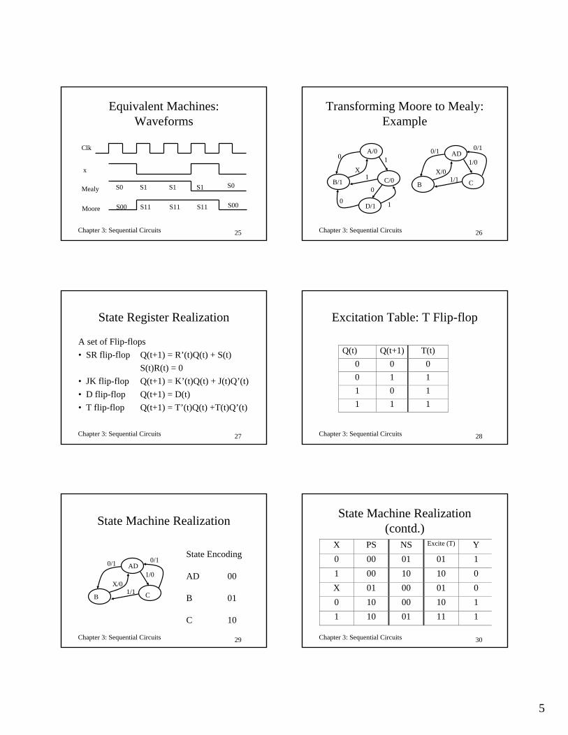
Chapter 3: Sequential Circuits 25
Equivalent Machines: Waveforms
S0 S1 S1 S1 S0Mealy
S00 S11 S11 S11 S00Moore
x
Clk
Chapter 3: Sequential Circuits 26
Transforming Moore to Mealy: Example
A/0
C/0B/1
D/1
10
X
0 1
1
0
AD
CB
1/0
1/1
0/10/1
X/0
Chapter 3: Sequential Circuits 27
State Register Realization
A set of Flip-flops• SR flip-flop Q(t+1) = R’(t)Q(t) + S(t)
S(t)R(t) = 0• JK flip-flop Q(t+1) = K’(t)Q(t) + J(t)Q’(t)• D flip-flop Q(t+1) = D(t)• T flip-flop Q(t+1) = T’(t)Q(t) +T(t)Q’(t)
Chapter 3: Sequential Circuits 28
Excitation Table: T Flip-flop
Q(t) Q(t+1) T(t)0 0 00 1 11 0 11 1 1
Chapter 3: Sequential Circuits 29
State Machine Realization
AD
CB
1/0
1/1
0/10/1
X/0
State Encoding
AD 00
B 01
C 10
Chapter 3: Sequential Circuits 30
State Machine Realization (contd.)
X PS NS Excite (T) Y0 00 01 01 11 00 10 10 0X 01 00 01 00 10 00 10 11 10 01 11 1
6
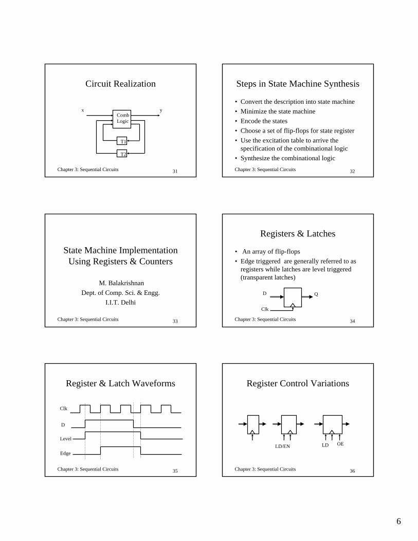
Chapter 3: Sequential Circuits 31
Circuit Realization
x y
T1
T2
CombLogic
Chapter 3: Sequential Circuits 32
Steps in State Machine Synthesis
• Convert the description into state machine• Minimize the state machine• Encode the states• Choose a set of flip-flops for state register• Use the excitation table to arrive the
specification of the combinational logic• Synthesize the combinational logic
Chapter 3: Sequential Circuits 33
State Machine Implementation Using Registers & Counters
M. BalakrishnanDept. of Comp. Sci. & Engg.
I.I.T. Delhi
Chapter 3: Sequential Circuits 34
Registers & Latches
• An array of flip-flops• Edge triggered are generally referred to as
registers while latches are level triggered (transparent latches)
D Q
Clk
Chapter 3: Sequential Circuits 35
Register & Latch Waveforms
Level
Edge
D
Clk
Chapter 3: Sequential Circuits 36
Register Control Variations
LD/EN OELD
7
Chapter 3: Sequential Circuits 37
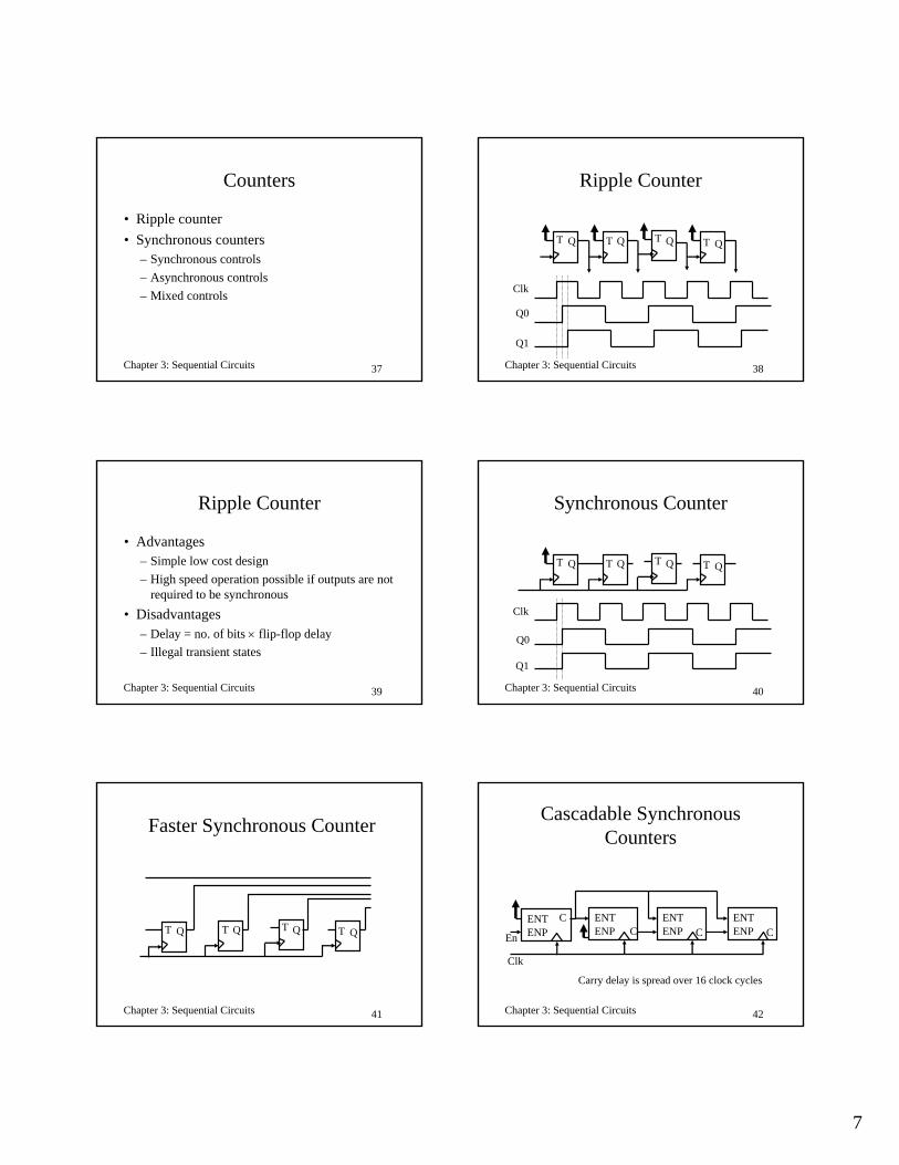
Counters
• Ripple counter• Synchronous counters
– Synchronous controls– Asynchronous controls– Mixed controls
Chapter 3: Sequential Circuits 38
Ripple Counter
T Q T Q T Q T Q
Clk
Q0
Q1
Chapter 3: Sequential Circuits 39
Ripple Counter
• Advantages– Simple low cost design– High speed operation possible if outputs are not
required to be synchronous• Disadvantages
– Delay = no. of bits × flip-flop delay– Illegal transient states
Chapter 3: Sequential Circuits 40
Synchronous Counter
T Q T Q T Q T Q
Q0
Q1
Clk
Chapter 3: Sequential Circuits 41
Faster Synchronous Counter
T Q T Q T Q T Q
Chapter 3: Sequential Circuits 42
Cascadable Synchronous Counters
ENTENP
ENTENP
ENTENP
CCCEn
Clk
Carry delay is spread over 16 clock cycles
ENTENP C
8
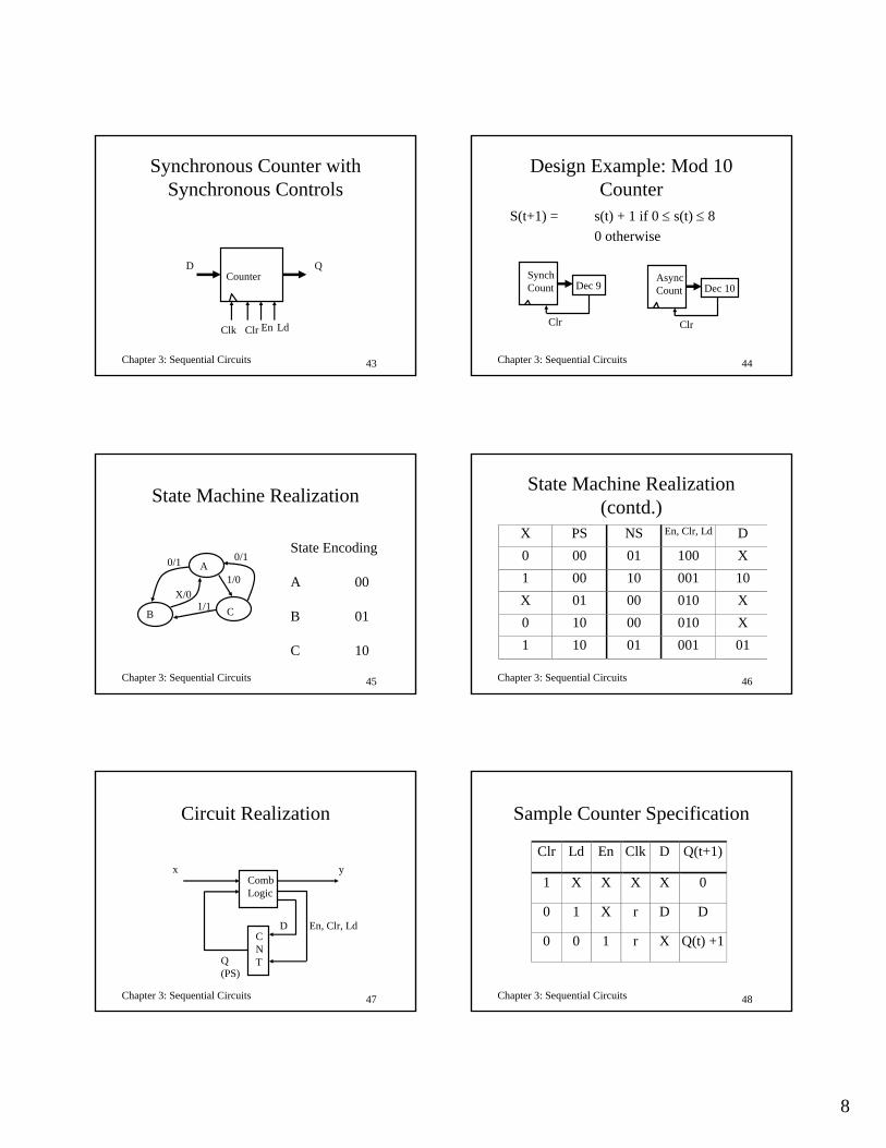
Chapter 3: Sequential Circuits 43
Synchronous Counter with Synchronous Controls
Clk Clr LdEn
D QCounter
Chapter 3: Sequential Circuits 44
Design Example: Mod 10 Counter
S(t+1) = s(t) + 1 if 0 ≤ s(t) ≤ 80 otherwise
Dec 9SynchCount Dec 10
AsyncCount
Clr Clr
Chapter 3: Sequential Circuits 45
State Machine Realization
A
CB
1/0
1/1
0/10/1
X/0
State Encoding
A 00
B 01
C 10
Chapter 3: Sequential Circuits 46
State Machine Realization (contd.)
X PS NS En, Clr, Ld D0 00 01 100 X1 00 10 001 10X 01 00 010 X0 10 00 010 X1 10 01 001 01
Chapter 3: Sequential Circuits 47
Circuit Realization
x y
CNT
CombLogic
En, Clr, LdD
Q(PS)
Chapter 3: Sequential Circuits 48
Sample Counter Specification
Clr Ld En Clk D Q(t+1)
1 X X X X 0
0 1 X r D D
0 0 1 r X Q(t) +1
9
Chapter 3: Sequential Circuits 49
Steps in State Machine Synthesisusing Counters
• Encode the states• Choose a counter with appropriate control
inputs to implement the state register• Use the counter functionality table to arrive
at the spec. of the combinational logic• Synthesize the combinational logic
Chapter 3: Sequential Circuits 50
Multiple State Machine Implementation & Clock Period
M. BalakrishnanDept. of Comp. Sci. & Engg.
I.I.T. Delhi
Chapter 3: Sequential Circuits 51
Steps in State Machine Synthesisusing Counters
• Encode the states• Choose a counter with appropriate control
inputs to implement the state register• Use the counter functionality table to arrive
at the spec. of the combinational logic• Synthesize the combinational logic
Chapter 3: Sequential Circuits 52
Applications of Sequential Machines
• Pattern matching– Overlapped or non-overlapped– Blocked or non-blocked
• Sequential decoding• Controllers• Memory based circuits
Chapter 3: Sequential Circuits 53
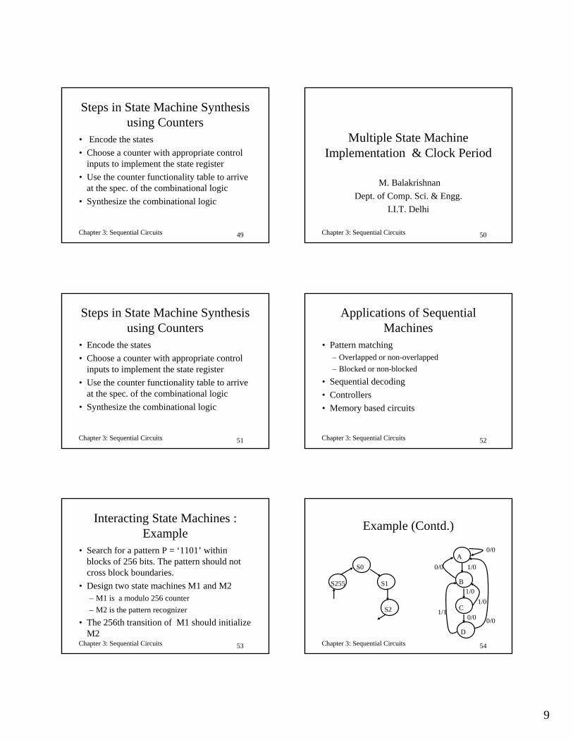
Interacting State Machines : Example
• Search for a pattern P = ‘1101’ within blocks of 256 bits. The pattern should not cross block boundaries.
• Design two state machines M1 and M2– M1 is a modulo 256 counter– M2 is the pattern recognizer
• The 256th transition of M1 should initialize M2
Chapter 3: Sequential Circuits 54
Example (Contd.)
S0
S1
S2
S255
A
B
C
D
0/0
1/00/0
1/0
0/0
1/01/1
0/0
10
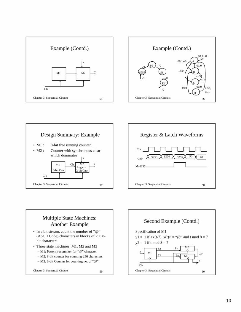
Chapter 3: Sequential Circuits 55
Example (Contd.)
M1 M2
Clk
x
y
Chapter 3: Sequential Circuits 56
Example (Contd.)
S0
S1
S2
S255
A
B
C
D
01/0
01/0
00/0
01/0
X0/0,11/1
-/0
-/0
-/0
-/0
-/1
00,1x/0
00,1x/0
1x/0
01/1
Chapter 3: Sequential Circuits 57
Design Summary: Example
• M1 : 8-bit free running counter• M2 : Counter with synchronous clear
which dominates
M1 M2
Clk
yClr
8-bit Cntr 2-bit CntrLogic +
x
Chapter 3: Sequential Circuits 58
Register & Latch Waveforms
Mod256
Cntr
Clk
S253 S254 S255 S0 S1
Chapter 3: Sequential Circuits 59
Multiple State Machines: Another Example
• In a bit stream, count the number of “@” (ASCII Code) characters in blocks of 256 8-bit characters
• Three state machines: M1, M2 and M3– M1: Pattern recognizer for “@” character– M2: 8-bit counter for counting 256 characters– M3: 8-bit Counter for counting no. of “@”
Chapter 3: Sequential Circuits 60
Second Example (Contd.)
Specification of M1y1 = 1 if <x(t-7)..x(t)> = “@” and t mod 8 = 7 y2 = 1 if t mod 8 = 7
M1
M2
M3
Clk
x
y
y2 En
y1 En Clr
11
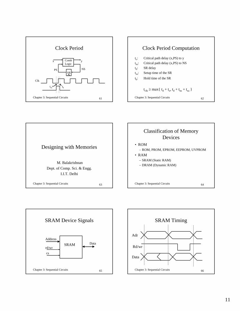
Chapter 3: Sequential Circuits 61
Clock Period
x y
PS NS
Clk
SR
CombLogic
thtsu
Chapter 3: Sequential Circuits 62
Clock Period Computation
to: Critical path delay (x,PS) to ytns: Critical path delay (x,PS) to NStd: SR delaytsu: Setup time of the SRth: Hold time of the SR
tclk ≥ max{ td + to, td + tns + tsu }
Chapter 3: Sequential Circuits 63
Designing with Memories
M. BalakrishnanDept. of Comp. Sci. & Engg.
I.I.T. Delhi
Chapter 3: Sequential Circuits 64
Classification of Memory Devices
• ROM– ROM, PROM, EPROM, EEPROM, UVPROM
• RAM– SRAM (Static RAM)– DRAM (Dynamic RAM)
Chapter 3: Sequential Circuits 65
SRAM Device Signals
AddressData
rd/wrcs
SRAM
Chapter 3: Sequential Circuits 66
SRAM Timing
Adr
Data
Rd/wr
12
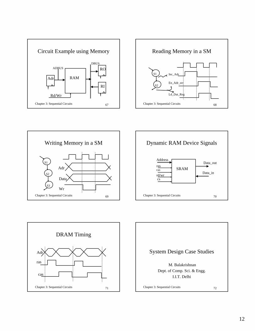
Chapter 3: Sequential Circuits 67
Circuit Example using Memory
RAM
RO
RI
Adr
Rd/Wr
ADBUSDBUS
Chapter 3: Sequential Circuits 68
Reading Memory in a SM
S1
S2En_Adr_src
Ld_Dat_Reg
Inc_Adr
Chapter 3: Sequential Circuits 69
Writing Memory in a SM
S1
S2
S3
Adr
Data
WrChapter 3: Sequential Circuits 70
Dynamic RAM Device Signals
Address
Data_inrd/wrcs
SRAMrascas
Data_out
Chapter 3: Sequential Circuits 71
DRAM Timing
ras
cas
Adr
Chapter 3: Sequential Circuits 72
System Design Case Studies
M. BalakrishnanDept. of Comp. Sci. & Engg.
I.I.T. Delhi
13
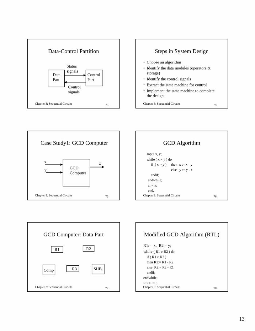
Chapter 3: Sequential Circuits 73
Data-Control Partition
DataPart
ControlPart
Statussignals
Controlsignals
Chapter 3: Sequential Circuits 74
Steps in System Design
• Choose an algorithm• Identify the data modules (operators &
storage)• Identify the control signals• Extract the state machine for control• Implement the state machine to complete
the design
Chapter 3: Sequential Circuits 75
Case Study1: GCD Computer
GCDComputer
x
y
z
Chapter 3: Sequential Circuits 76
GCD Algorithm
Input x, y;while ( x ≠ y ) do
if ( x > y ) then x := x - yelse y := y - x
endif;endwhile;z := x;end.
Chapter 3: Sequential Circuits 77
GCD Computer: Data Part
R2R1
R3Comp SUB
Chapter 3: Sequential Circuits 78
Modified GCD Algorithm (RTL)
R1:= x, R2:= y;while ( R1 ≠ R2 ) do
if ( R1 > R2 ) then R1:= R1 - R2else R2:= R2 - R1endif;
endwhile;R3:= R1;
14
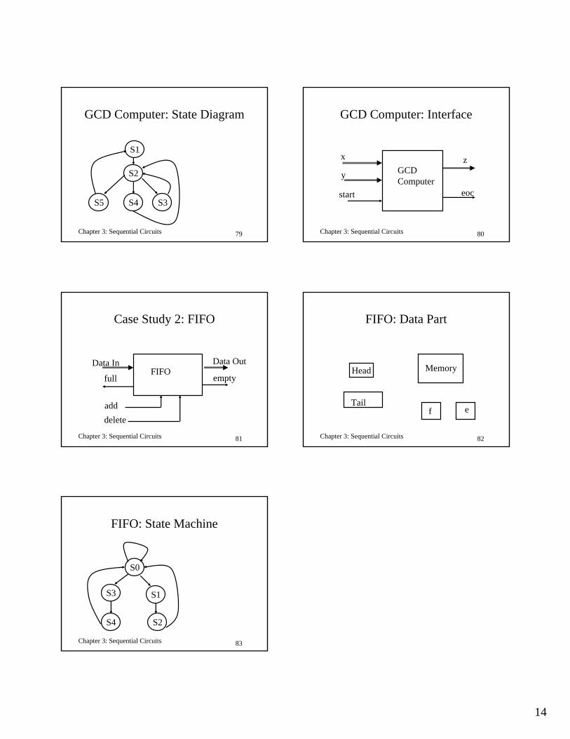
Chapter 3: Sequential Circuits 79
GCD Computer: State Diagram
S1
S2
S3S4S5
Chapter 3: Sequential Circuits 80
GCD Computer: Interface
GCDComputer
x
y
z
start eoc
Chapter 3: Sequential Circuits 81
Case Study 2: FIFO
FIFOData In Data Out
emptyfull
adddelete
Chapter 3: Sequential Circuits 82
FIFO: Data Part
Head
Tailf e
Memory
Chapter 3: Sequential Circuits 83
FIFO: State Machine
S0
S1S3
S4 S2
1
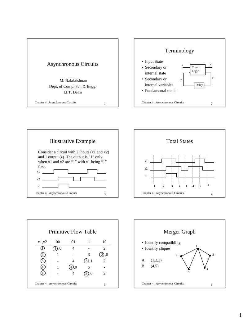
Chapter 4: Asynchronous Circuits 1
Asynchronous Circuits
M. BalakrishnanDept. of Comp. Sci. & Engg.
I.I.T. Delhi
Chapter 4: Asynchronous Circuits 2
Terminology
• Input State• Secondary or
internal state • Secondary or
internal variables• Fundamental mode
Comb.Logic
Delay
x z
Yy
Chapter 4: Asynchronous Circuits 3
Illustrative Example
Consider a circuit with 2 inputs (x1 and x2) and 1 output (z). The output is “1” only when x1 and x2 are “1” with x1 being “1” first.
x1
x2
z
Chapter 4: Asynchronous Circuits 4
Total States
x1
x2
z
1 2 3 4 1 4 5 1
Chapter 4: Asynchronous Circuits 5
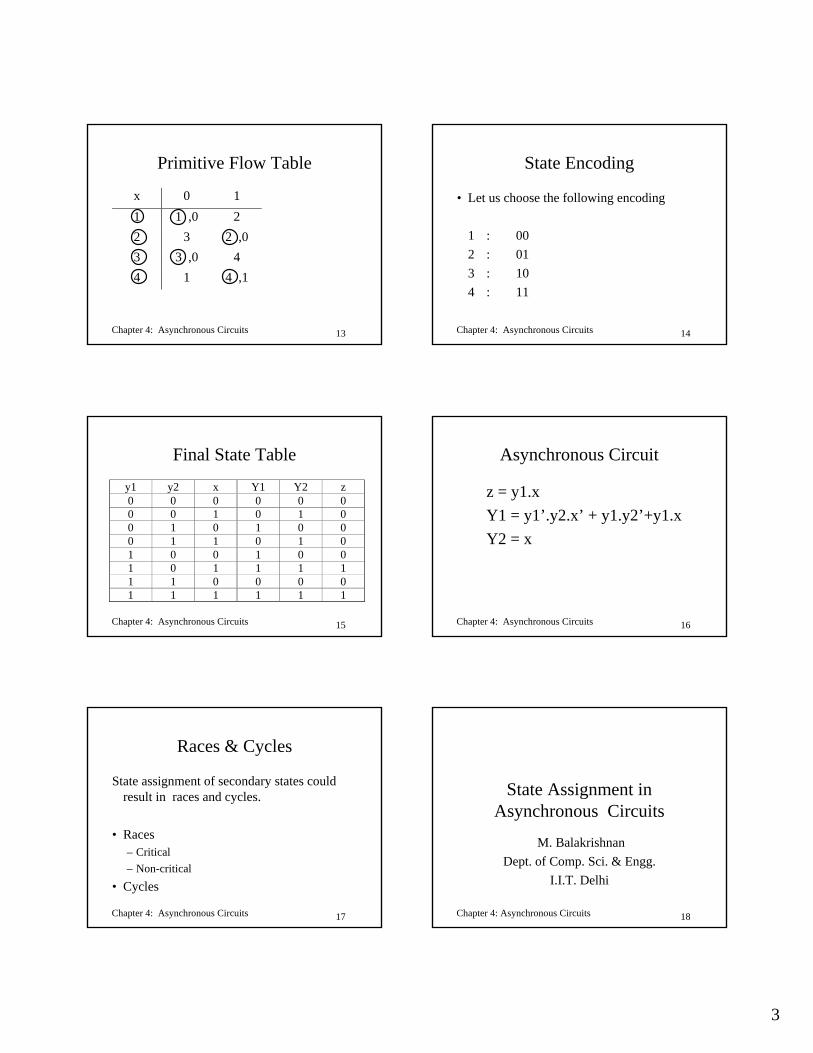
Primitive Flow Table
x1,x2 00 01 11 101 1 ,0 4 - 22 1 - 3 2 ,03 - 4 3 ,1 24 1 4 ,0 5 -5 - 4 5 ,0 2
Chapter 4: Asynchronous Circuits 6
Merger Graph
• Identify compatibility• Identify cliques
A (1,2,3)B (4,5)
1
2
3
4
5
2
Chapter 4: Asynchronous Circuits 7
Reduced Flow Table
x1, x2 00 01 11 10A 1 ,0 4 3 ,1 2 ,0B 1 4 ,0 5 ,0 2
Chapter 4: Asynchronous Circuits 8
Final State Table
x1, x2 00 01 11 100 0 ,0 1 ,0 0 ,1 0 ,01 0 ,0 1 ,0 1 ,0 0 ,0
z = y’x1x2
y = x1’x2 + yx2
Chapter 4: Asynchronous Circuits 9
Asynchronous Circuit
z = y’x1x2y = x1’x2 + yx2
Chapter 4: Asynchronous Circuits 10
Asynchronous Sequential Circuit Design
M. BalakrishnanDept. of Comp. Sci. & Engg.
I.I.T. Delhi
Chapter 4: Asynchronous Circuits 11
Another Example
Consider a circuit with 1 input (x ) and 1 output (z). The output should suppress every alternate pulse on the input starting with the first.
x
z
Chapter 4: Asynchronous Circuits 12
Total States
1
x
z
2 3 4 1
3
Chapter 4: Asynchronous Circuits 13
Primitive Flow Table
x 0 11 1 ,0 22 3 2 ,03 3 ,0 44 1 4 ,1
Chapter 4: Asynchronous Circuits 14
State Encoding
• Let us choose the following encoding
1 : 002 : 013 : 104 : 11
Chapter 4: Asynchronous Circuits 15
Final State Table
y1 y2 x Y1 Y2 z0 0 0 0 0 00 0 1 0 1 00 1 0 1 0 00 1 1 0 1 01 0 0 1 0 01 0 1 1 1 11 1 0 0 0 01 1 1 1 1 1
Chapter 4: Asynchronous Circuits 16
Asynchronous Circuit
z = y1.xY1 = y1’.y2.x’ + y1.y2’+y1.xY2 = x
Chapter 4: Asynchronous Circuits 17
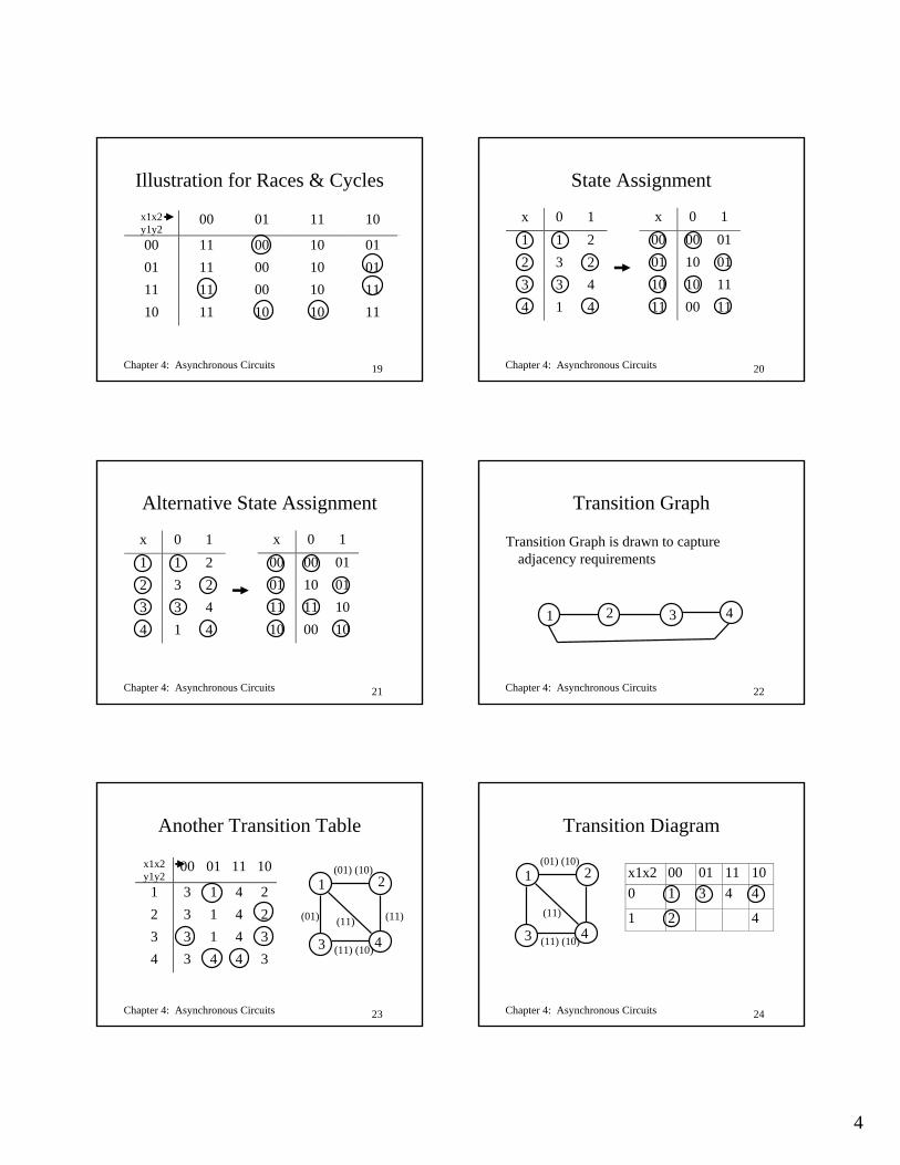
Races & Cycles
State assignment of secondary states could result in races and cycles.
• Races– Critical– Non-critical
• Cycles
Chapter 4: Asynchronous Circuits 18
State Assignment in Asynchronous Circuits
M. BalakrishnanDept. of Comp. Sci. & Engg.
I.I.T. Delhi
4
Chapter 4: Asynchronous Circuits 19
Illustration for Races & Cycles
x1x2y1y2
00 01 11 10
00 11 00 10 0101 11 00 10 0111 11 00 10 1110 11 10 10 11
Chapter 4: Asynchronous Circuits 20
State Assignment
x 0 11 1 22 3 23 3 44 1 4
x 0 100 00 0101 10 0110 10 1111 00 11
Chapter 4: Asynchronous Circuits 21
Alternative State Assignment
x 0 11 1 22 3 23 3 44 1 4
x 0 100 00 0101 10 0111 11 1010 00 10
Chapter 4: Asynchronous Circuits 22
Transition Graph
Transition Graph is drawn to capture adjacency requirements
1 2 3 4
Chapter 4: Asynchronous Circuits 23
Another Transition Table
x1x2y1y2
00 01 11 10
1 3 1 4 22 3 1 4 23 3 1 4 34 3 4 4 3
1 2
3 4
(01) (10)
(11)(11)
(11) (10)
(01)
Chapter 4: Asynchronous Circuits 24
Transition Diagram
x1x2 00 01 11 100 1 3 4 4
1 2 4
1 2
3 4
(01) (10)
(11)
(11) (10)
5
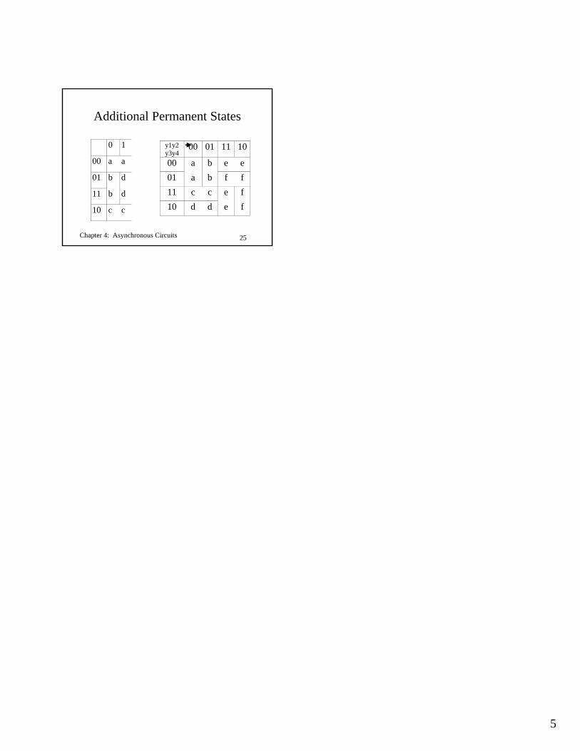
Chapter 4: Asynchronous Circuits 25
Additional Permanent States
0 1
00 a a
01 b d
11 b d
10 c c
y1y2y3y4
00 01 11 10
00 a b e e01 a b f f11 c c e f10 d d e f
1
Chapter 5: Microprogrammed Control 1
Microprogrammed Control
M. BalakrishnanDept. of Comp. Sci. & Engg.
I.I.T. Delhi
Chapter 5: Microprogrammed Control 2
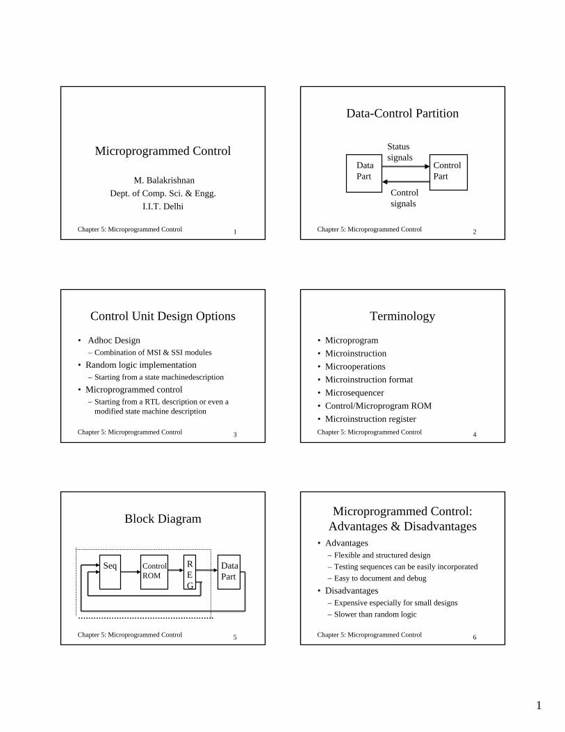
Data-Control Partition
DataPart
ControlPart
Statussignals
Controlsignals
Chapter 5: Microprogrammed Control 3
Control Unit Design Options
• Adhoc Design– Combination of MSI & SSI modules
• Random logic implementation– Starting from a state machinedescription
• Microprogrammed control– Starting from a RTL description or even a
modified state machine description
Chapter 5: Microprogrammed Control 4
Terminology
• Microprogram• Microinstruction• Microoperations• Microinstruction format• Microsequencer• Control/Microprogram ROM• Microinstruction register
Chapter 5: Microprogrammed Control 5
Block Diagram
Seq ControlROM
REG
DataPart
Chapter 5: Microprogrammed Control 6
Microprogrammed Control: Advantages & Disadvantages
• Advantages– Flexible and structured design– Testing sequences can be easily incorporated– Easy to document and debug
• Disadvantages– Expensive especially for small designs– Slower than random logic
2
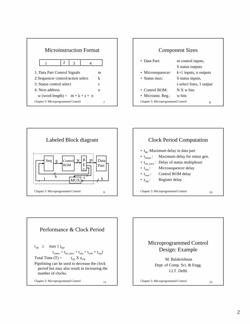
Chapter 5: Microprogrammed Control 7
Microinstruction Format
1: Data Part Control Signals m2:Sequencer control/action select k3: Status control select s4: Next address n
w (word length) = m + k + s + n
1 2 3 4
Chapter 5: Microprogrammed Control 8
Component Sizes
• Data Part: m control inputs,S status outputs
• Microsequencer: k+1 inputs, n outputs• Status mux: S status inputs,
s select lines, 1 output• Control ROM: N Χ w bits• Microinst. Reg.: w bits
Chapter 5: Microprogrammed Control 9
Labeled Block diagram
Seq ControlROM
REG
DataPart
MUX1
n w m
Ssk
Chapter 5: Microprogrammed Control 10
Clock Period Computation
• tdp :Maximum delay in data part • tstatus : Maximum delay for status gen.• tsta_mux : Delay of status multiplexer• tseq : Microsequencer delay• trom : Control ROM delay• treg : Register delay
Chapter 5: Microprogrammed Control 11
Performance & Clock Period
tclk ≥ max { tdp, tstatus + tsta_mux + tseq + trom + treg}
Total Time (T) = tclk Χ nclk
Pipelining can be used to decrease the clock period but may also result in increasing the number of clocks.
Chapter 5: Microprogrammed Control 12
Microprogrammed Control Design: Example
M. BalakrishnanDept. of Comp. Sci. & Engg.
I.I.T. Delhi
3
Chapter 5: Microprogrammed Control 13
Design Steps
• Design the datapart and identify the control and status signals
• Design the microsequencer based on the branchings required
• From the schedule of operations finalize the size of the control ROM
• Finalize the microinstruction format• Generate the microprogram
Chapter 5: Microprogrammed Control 14
Case Study: GCD Computer
GCDComputer
x
y
z
starteoc
Chapter 5: Microprogrammed Control 15
GCD Algorithm
s: wait till (start=1);input x, y; eoc := 0;while ( x ≠ y ) do
if ( x > y ) then x := x - yelse y := y - x
endif;endwhile;z := x; eoc := 1; go to s; end. Chapter 5: Microprogrammed Control 16
GCD Computer: Data Part
R2R1
R3Comp SUB
eoc
Chapter 5: Microprogrammed Control 17
GCD Computer: State Diagram
S0
S2
S4S5S6
S1
S3
Chapter 5: Microprogrammed Control 18
Control Flow Requirements
• Next microinstruction• If (cond) then …
else “m(i + 1)”cond = {start’, .eq.,.gt.}
• Go to “m(0)”
4
Chapter 5: Microprogrammed Control 19
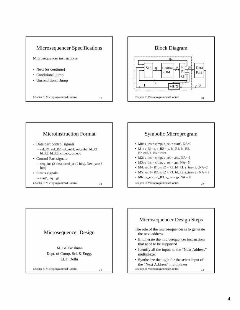
Microsequencer Specifications
Microsequencer instructions
• Next (or continue)• Conditional jump• Unconditional Jump
Chapter 5: Microprogrammed Control 20
Block Diagram
Seq ControlROM
REG
DataPart
MUX1
n w m
Ssk
n
Chapter 5: Microprogrammed Control 21
Microinstruction Format
• Data part control signals– sel_R1, sel_R2, sel_sub1, sel_seb2, ld_R1,
ld_R2, ld_R3, clr_eoc, pr_eoc• Control Part signals
– seq._ins (2 bits), cond_sel(2 bits), Next_adr(3 bits)
• Status signals– start’, .eq., .gt.
Chapter 5: Microprogrammed Control 22
Symbolic Microprogram
• M0: s_ins = cjmp, c_sel = start’, NA=0• M1: s_R1=x, s_R2 = y, ld_R1, ld_R2,
clr_eoc, s_ins = cont• M2: s_ins = cjmp, c_sel = .eq., NA= 6 • M3: s_ins = cjmp, c_sel = .gt., NA= 5• M4: sub1= R1, sub2 = R2, ld_R1, s_ins= jp ,NA=2• M5: sub1= R2, sub2 = R1, ld_R2, s_ins= jp, NA = 2• M6: pr_eoc, ld_R3, s_ins = jp, NA = 0
Chapter 5: Microprogrammed Control 23
Microsequencer Design
M. BalakrishnanDept. of Comp. Sci. & Engg.
I.I.T. Delhi
Chapter 5: Microprogrammed Control 24
Microsequencer Design Steps
The role of the microsequencer is to generate the next address.
• Enumerate the microsequencer instructions that need to be supported
• Identify all the inputs to the “Next Address” multiplexer
• Synthesize the logic for the select input of the “Next Address” multiplexer
5
Chapter 5: Microprogrammed Control 25
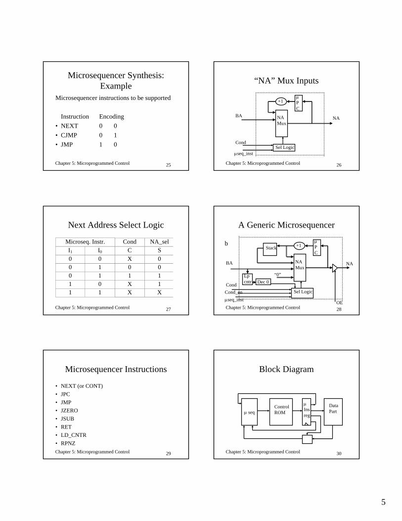
Microsequencer Synthesis: Example
Microsequencer instructions to be supported
Instruction Encoding• NEXT 0 0• CJMP 0 1• JMP 1 0
Chapter 5: Microprogrammed Control 26
“NA” Mux Inputs
NAMux
µPC
+1
NABA
Cond
µseq_instSel Logic
Chapter 5: Microprogrammed Control 27
Next Address Select Logic
Microseq. Instr. Cond NA_selI1 I0 C S0 0 X 00 1 0 00 1 1 11 0 X 11 1 X X
Chapter 5: Microprogrammed Control 28
A Generic Microsequencer
NAMux
µPC
+1
BA
Cond
µseq_inst
Sel Logic
b
“0”Dec 0
Lpcntr
NA
Stack
Cond_en
OE
Chapter 5: Microprogrammed Control 29
Microsequencer Instructions
• NEXT (or CONT)• JPC• JMP• JZERO• JSUB• RET• LD_CNTR• RPNZ
Chapter 5: Microprogrammed Control 30
Block Diagram
µ seqControlROM
µInsreg
DataPart
6
Chapter 5: Microprogrammed Control 31
Timing Diagram
Clk
NA
µseq_instr
a a+1
JSUB b
b
NEXT
MI[a] MI[a+1] MI[b]µinstr
Chapter 5: Microprogrammed Control 32
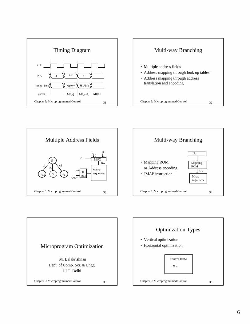
Multi-way Branching
• Multiple address fields• Address mapping through look up tables• Address mapping through address
translation and encoding
Chapter 5: Microprogrammed Control 33
Multiple Address Fields
Si
Si+1 Sj Sk
Micro-sequencer
BAc1
c2c3
Sta.mux
c2+c3
c3
j k
MUX0 1
Chapter 5: Microprogrammed Control 34
Multi-way Branching
• Mapping ROMor Address encoding
• JMAP instruction
IR
Mapping ROM
Microsequencer
BA
Chapter 5: Microprogrammed Control 35
Microprogram Optimization
M. BalakrishnanDept. of Comp. Sci. & Engg.
I.I.T. Delhi
Chapter 5: Microprogrammed Control 36
Optimization Types
• Vertical optimization• Horizontal optimization
Control ROM
m X n
7
Chapter 5: Microprogrammed Control 37
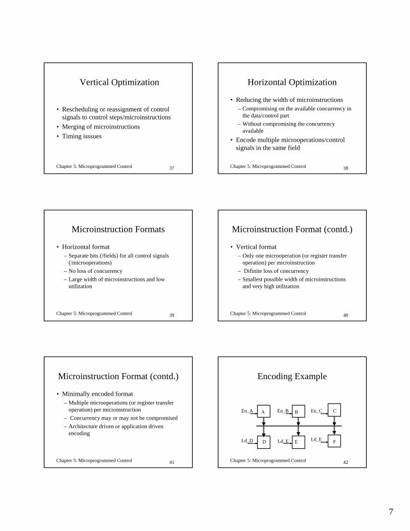
Vertical Optimization
• Rescheduling or reassignment of control signals to control steps/microinstructions
• Merging of microinstructions• Timing isssues
Chapter 5: Microprogrammed Control 38
Horizontal Optimization
• Reducing the width of microinstructions– Compromising on the available concurrency in
the data/control part– Without compromising the concurrency
available• Encode multiple microoperations/control
signals in the same field
Chapter 5: Microprogrammed Control 39
Microinstruction Formats
• Horizontal format– Separate bits (/fields) for all control signals
(/microoperations)– No loss of concurrency– Large width of microinstructions and low
utilization
Chapter 5: Microprogrammed Control 40
Microinstruction Format (contd.)
• Vertical format– Only one microoperation (or register transfer
operation) per microinstruction– Difinite loss of concurrency– Smallest possible width of microinstructions
and very high utilization
Chapter 5: Microprogrammed Control 41
Microinstruction Format (contd.)
• Minimally encoded format– Multiple microoperations (or register transfer
operation) per microinstruction– Concurrency may or may not be compromised– Architecture driven or application driven
encoding
Chapter 5: Microprogrammed Control 42
Encoding Example
A B C
D E F
En_A En_B En_C
Ld_D Ld_E Ld_E
8
Chapter 5: Microprogrammed Control 43
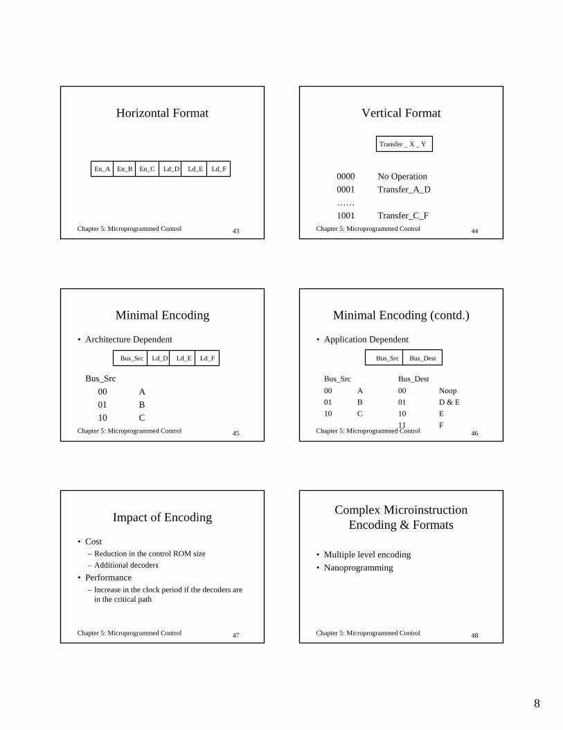
Horizontal Format
En_A En_B En_C Ld_D Ld_E Ld_F
Chapter 5: Microprogrammed Control 44
Vertical Format
0000 No Operation0001 Transfer_A_D……1001 Transfer_C_F
Transfer _ X _ Y
Chapter 5: Microprogrammed Control 45
Minimal Encoding
• Architecture Dependent
Bus_Src00 A01 B10 C
Bus_Src Ld_D Ld_E Ld_F
Chapter 5: Microprogrammed Control 46
Minimal Encoding (contd.)
• Application Dependent
Bus_Src Bus_Dest00 A 00 Noop01 B 01 D & E10 C 10 E
11 F
Bus_Src Bus_Dest
Chapter 5: Microprogrammed Control 47
Impact of Encoding
• Cost– Reduction in the control ROM size– Additional decoders
• Performance– Increase in the clock period if the decoders are
in the critical path
Chapter 5: Microprogrammed Control 48
Complex Microinstruction Encoding & Formats
• Multiple level encoding• Nanoprogramming
9
Chapter 5: Microprogrammed Control 49
Microinstruction Optimization
M. BalakrishnanDept. of Comp. Sci. & Engg.
I.I.T. Delhi
Chapter 5: Microprogrammed Control 50
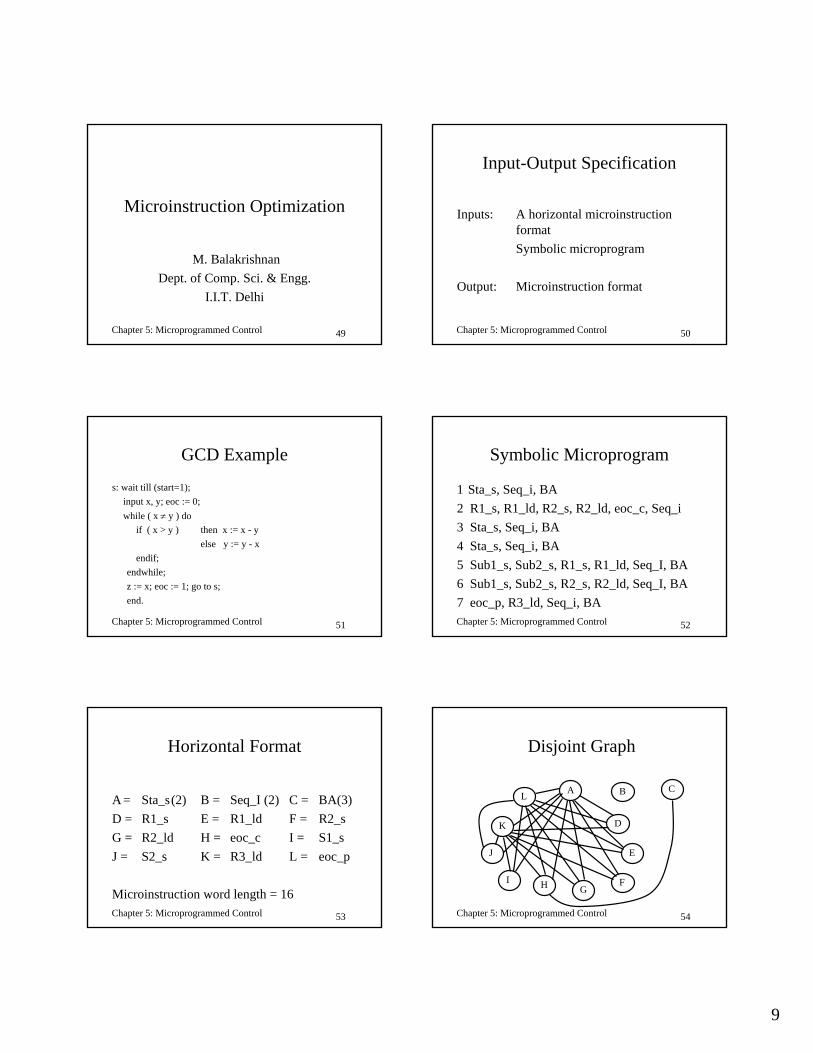
Input-Output Specification
Inputs: A horizontal microinstruction formatSymbolic microprogram
Output: Microinstruction format
Chapter 5: Microprogrammed Control 51
GCD Example
s: wait till (start=1);input x, y; eoc := 0;while ( x ≠ y ) do
if ( x > y ) then x := x - yelse y := y - x
endif;endwhile;z := x; eoc := 1; go to s; end.
Chapter 5: Microprogrammed Control 52
Symbolic Microprogram
1 Sta_s, Seq_i, BA2 R1_s, R1_ld, R2_s, R2_ld, eoc_c, Seq_i3 Sta_s, Seq_i, BA4 Sta_s, Seq_i, BA5 Sub1_s, Sub2_s, R1_s, R1_ld, Seq_I, BA6 Sub1_s, Sub2_s, R2_s, R2_ld, Seq_I, BA7 eoc_p, R3_ld, Seq_i, BA
Chapter 5: Microprogrammed Control 53
Horizontal Format
A = Sta_s(2) B = Seq_I (2) C = BA(3)D = R1_s E = R1_ld F = R2_sG = R2_ld H = eoc_c I = S1_sJ = S2_s K = R3_ld L = eoc_p
Microinstruction word length = 16 Chapter 5: Microprogrammed Control 54
Disjoint Graph
A B C
D
E
FGHI
K
L
J
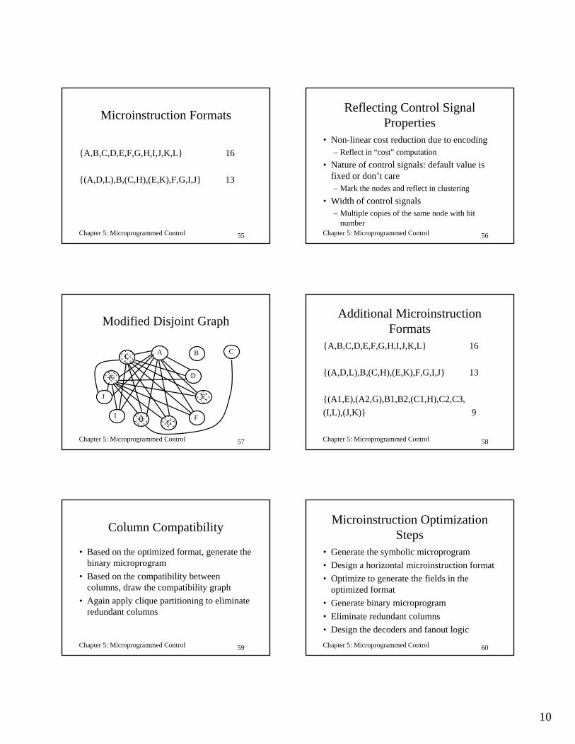
10
Chapter 5: Microprogrammed Control 55
Microinstruction Formats
{A,B,C,D,E,F,G,H,I,J,K,L} 16
{(A,D,L),B,(C,H),(E,K),F,G,I,J} 13
Chapter 5: Microprogrammed Control 56
Reflecting Control Signal Properties
• Non-linear cost reduction due to encoding– Reflect in “cost” computation
• Nature of control signals: default value is fixed or don’t care– Mark the nodes and reflect in clustering
• Width of control signals– Multiple copies of the same node with bit
number
Chapter 5: Microprogrammed Control 57
Modified Disjoint Graph
A B C
D
E
FGHI
K
L
J
Chapter 5: Microprogrammed Control 58
Additional Microinstruction Formats
{A,B,C,D,E,F,G,H,I,J,K,L} 16
{(A,D,L),B,(C,H),(E,K),F,G,I,J} 13
{(A1,E),(A2,G),B1,B2,(C1,H),C2,C3,(I,L),(J,K)} 9
Chapter 5: Microprogrammed Control 59
Column Compatibility
• Based on the optimized format, generate the binary microprogram
• Based on the compatibility between columns, draw the compatibility graph
• Again apply clique partitioning to eliminate redundant columns
Chapter 5: Microprogrammed Control 60
Microinstruction Optimization Steps
• Generate the symbolic microprogram• Design a horizontal microinstruction format• Optimize to generate the fields in the
optimized format• Generate binary microprogram• Eliminate redundant columns• Design the decoders and fanout logic
1
Chapter 6: Introduction to VHDL 1
Introduction to VHDL
M. BalakrishnanDept of Computer Science & Engg.
I.I.T. Delhi
Chapter 6: Introduction to VHDL 2
Domains of Description :Gajski’s Y-Chart
Behavioraldomain
Structuraldomain
Physical domain
Level of abstraction
VHDL models
Chapter 6: Introduction to VHDL 3
VHDL Development
• US DoD initiated in 80’s• Very High Speed ASIC Description
Language• Initial objective was modeling only and thus
only a simulator was envisaged• Subsequently tools for VHDL synthesis
were developed
Chapter 6: Introduction to VHDL 4
HDL Requirements
• Abstraction• Modularity• Concurrency• Hierarchy
Chapter 6: Introduction to VHDL 5
Abstraction
VHDL supports description of components as well as systems at various levels of abstraction
• Gate and component delays• Clock cycles• Abstract behavior without any notion of
delays
Chapter 6: Introduction to VHDL 6
Modularity
• Every component in VHDL is referred to as an entity and has a clear interface
• The interface is called an entity declaration • The “internals” of the component are
referred to as the architecture declaration• There can be multiple architectures at even
different levels of abstraction associated with the same entity
2
Chapter 6: Introduction to VHDL 7
VHDL Example
a
bcAND
Chapter 6: Introduction to VHDL 8
VHDL Description: AND gate
entity AND2 isport (a, b: in bit ;
c : out bit);end AND2;
architecture beh of AND2 isbegin
c <= a and b;end beh;
Chapter 6: Introduction to VHDL 9
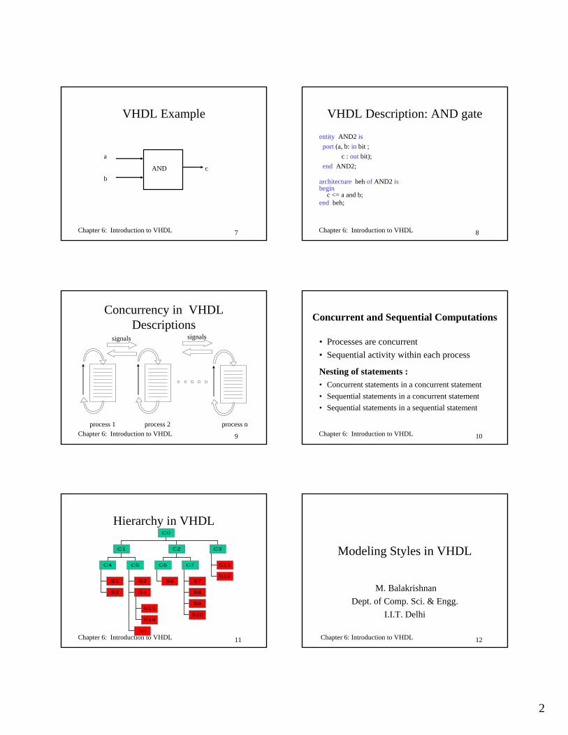
Concurrency in VHDL Descriptions
signals
process 1 process 2 process n
signals
Chapter 6: Introduction to VHDL 10
Concurrent and Sequential Computations
• Processes are concurrent• Sequential activity within each process
Nesting of statements :• Concurrent statements in a concurrent statement• Sequential statements in a concurrent statement• Sequential statements in a sequential statement
Chapter 6: Introduction to VHDL 11
Hierarchy in VHDL
S1
S2
C4
S3
S13
S14
S4
S5
C5
C1
S6
C6
S7
S8
S9
S10
C7
C2
S11
S12
C3
C0
Chapter 6: Introduction to VHDL 12
Modeling Styles in VHDL
M. BalakrishnanDept. of Comp. Sci. & Engg.
I.I.T. Delhi
3
Chapter 6: Introduction to VHDL 13
Modeling Styles• Semantic model of VHDL
• Structural description
• Data Flow description
• Algorithmic description
• RTL description
Chapter 6: Introduction to VHDL 14
Modeling Choices in VHDL• Behavioral and Structural Domains
– Several Levels of Abstraction• Multiple Styles of Behavioral Description:
– Data Flow Style (concurrent)– Procedural Style (sequential)
• Combinations, variations and special cases of these, e.g.,– special case of data flow style - FSM described using
guarded blocks– special case of procedural style - FSM described using
case statement in a process
Chapter 6: Introduction to VHDL 15
Structural Description• Carries same information as a NET LIST• Net List = (Component instances) + (Nets)• Structural Description in VHDL =
(Signals) + (Component instances + Port maps)• Many sophisticated features in VHDL to make it
more versatile:* Variety of signal types* Generic components* Generate statements for creating arrays of component instances* Flexibility in binding components to design entities and
architecturesChapter 6: Introduction to VHDL 16
Behavioral Description• Procedural
(textual order => execution order)
• Sequential statements• Control constructs alter
normal sequential flow
Called Behavioral description in VHDL
• Non-procedural (textual order NOT =>
execution order)• Concurrent statements• Data flow (or rather data
dependency restricts concurrency)
Called Data flow description in VHDL
Chapter 6: Introduction to VHDL 17
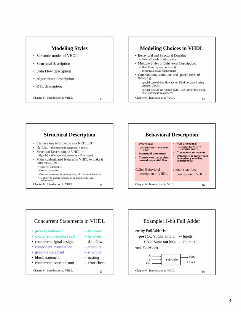
Concurrent Statements in VHDL
• process statement -- behavior• concurrent procedure call -- behavior• concurrent signal assign. -- data flow• component instantiation -- structure• generate statement -- structure• block statement -- nesting• concurrent assertion stmt -- error check
Chapter 6: Introduction to VHDL 18
Example: 1-bit Full Adder
entity FullAdder isport (X, Y, Cin: in bit; -- Inputs
Cout, Sum: out bit); -- Outputsend FullAdder;
XY
Cin
Sum
CoutFullAdder
4
Chapter 6: Introduction to VHDL 19
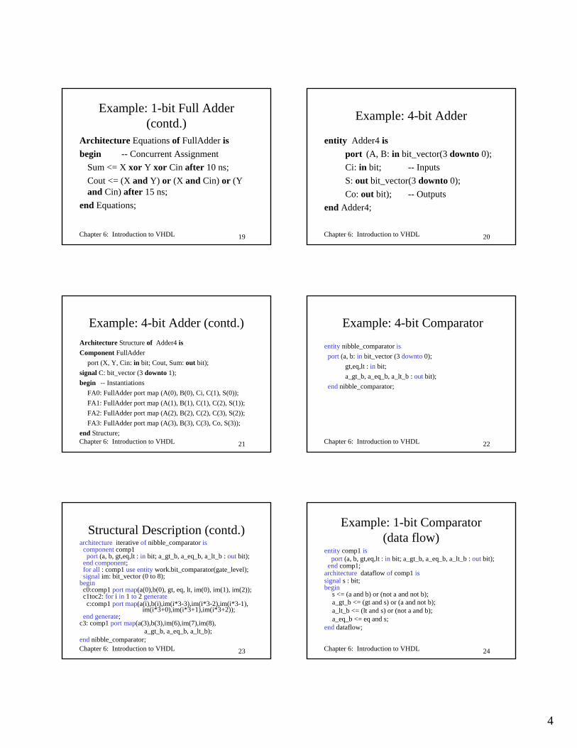
Example: 1-bit Full Adder (contd.)
Architecture Equations of FullAdder isbegin -- Concurrent Assignment
Sum <= X xor Y xor Cin after 10 ns;Cout <= (X and Y) or (X and Cin) or (Y and Cin) after 15 ns;
end Equations;
Chapter 6: Introduction to VHDL 20
Example: 4-bit Adder
entity Adder4 isport (A, B: in bit_vector(3 downto 0);Ci: in bit; -- InputsS: out bit_vector(3 downto 0);Co: out bit); -- Outputs
end Adder4;
Chapter 6: Introduction to VHDL 21
Example: 4-bit Adder (contd.)Architecture Structure of Adder4 isComponent FullAdder
port (X, Y, Cin: in bit; Cout, Sum: out bit);signal C: bit_vector (3 downto 1);begin -- Instantiations
FA0: FullAdder port map (A(0), B(0), Ci, C(1), S(0));FA1: FullAdder port map (A(1), B(1), C(1), C(2), S(1));FA2: FullAdder port map (A(2), B(2), C(2), C(3), S(2));FA3: FullAdder port map (A(3), B(3), C(3), Co, S(3));
end Structure;Chapter 6: Introduction to VHDL 22
Example: 4-bit Comparator
entity nibble_comparator isport (a, b: in bit_vector (3 downto 0);
gt,eq,lt : in bit;a_gt_b, a_eq_b, a_lt_b : out bit);
end nibble_comparator;
Chapter 6: Introduction to VHDL 23
Structural Description (contd.)architecture iterative of nibble_comparator is
component comp1port (a, b, gt,eq,lt : in bit; a_gt_b, a_eq_b, a_lt_b : out bit);
end component;for all : comp1 use entity work.bit_comparator(gate_level);signal im: bit_vector (0 to 8);
beginc0:comp1 port map(a(0),b(0), gt, eq, lt, im(0), im(1), im(2));c1toc2: for i in 1 to 2 generate
c:comp1 port map(a(i),b(i),im(i*3-3),im(i*3-2),im(i*3-1), im(i*3+0),im(i*3+1),im(i*3+2));
end generate;c3: comp1 port map(a(3),b(3),im(6),im(7),im(8),
a_gt_b, a_eq_b, a_lt_b);end nibble_comparator;
Chapter 6: Introduction to VHDL 24
Example: 1-bit Comparator (data flow)
entity comp1 isport (a, b, gt,eq,lt : in bit; a_gt_b, a_eq_b, a_lt_b : out bit);
end comp1;architecture dataflow of comp1 issignal s : bit;begin
s <= (a and b) or (not a and not b);a_gt_b <= (gt and s) or (a and not b);a_lt_b <= (lt and s) or (not a and b);a_eq_b <= eq and s;
end dataflow;
5
Chapter 6: Introduction to VHDL 25
References
• Digital Systems Design Using VHDLCharles H. Roth, Jr., PWS Publishing Co.Chapter 2 (pp. 44 to 84)
• The Designer’s Guide to VHDLPeter J. Ashenden, Morgon Kaufmann
Chapter 6: Introduction to VHDL 26
Behavioral Description in VHDL
M. BalakrishnanDept. of Comp. Sci. & Engg.
I.I.T. Delhi
Chapter 6: Introduction to VHDL 27
Modeling Styles• Semantic model of VHDL
• Structural description
• Data Flow description
• Algorithmic description
• RTL description
Chapter 6: Introduction to VHDL 28
Concurrent Statements in VHDL
• process statement -- behavior• concurrent procedure call -- behavior• concurrent signal assign. -- data flow• component instantiation -- structure• generate statement -- structure• block statement -- nesting• concurrent assertion stmt -- error check
Chapter 6: Introduction to VHDL 29
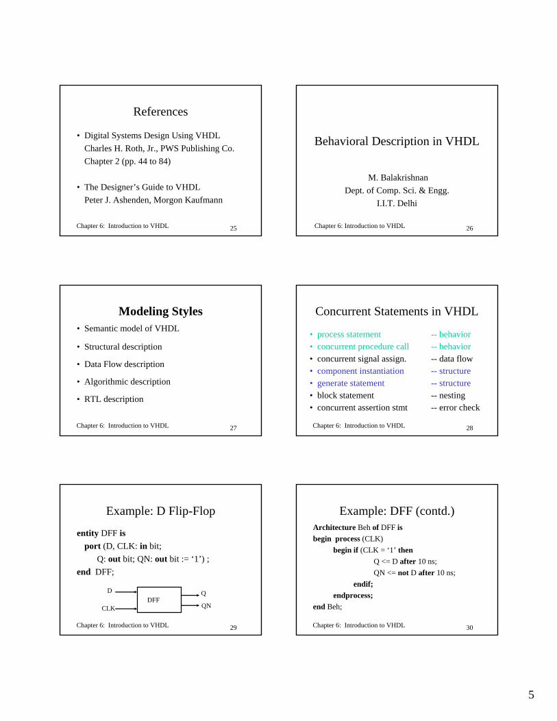
Example: D Flip-Flop
entity DFF isport (D, CLK: in bit;
Q: out bit; QN: out bit := ‘1’) ; end DFF;
D
CLK
Q
QNDFF
Chapter 6: Introduction to VHDL 30
Example: DFF (contd.)Architecture Beh of DFF isbegin process (CLK)
begin if (CLK = ‘1’ thenQ <= D after 10 ns;QN <= not D after 10 ns;
endif;endprocess;
end Beh;
6
Chapter 6: Introduction to VHDL 31
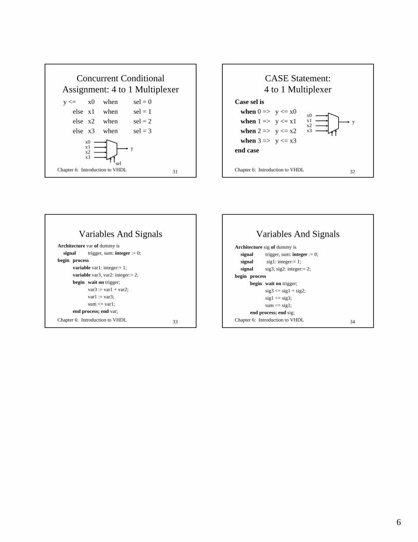
Concurrent Conditional Assignment: 4 to 1 Multiplexery <= x0 when sel = 0
else x1 when sel = 1else x2 when sel = 2else x3 when sel = 3
x0x1x2x3
sel
y
Chapter 6: Introduction to VHDL 32
CASE Statement: 4 to 1 Multiplexer
Case sel iswhen 0 => y <= x0when 1 => y <= x1when 2 => y <= x2when 3 => y <= x3
end case
x0x1x2x3
y
Chapter 6: Introduction to VHDL 33
Variables And SignalsArchitecture var of dummy is
signal trigger, sum: integer := 0;begin process
variable var1: integer:= 1;variable var3, var2: integer:= 2;begin wait on trigger;
var3 := var1 + var2;var1 := var3;sum <= var1;
end process; end var;
Chapter 6: Introduction to VHDL 34
Variables And SignalsArchitecture sig of dummy is
signal trigger, sum: integer := 0;signal sig1: integer:= 1;signal sig3, sig2: integer:= 2;
begin processbegin wait on trigger;
sig3 <= sig1 + sig2;sig1 <= sig3;sum <= sig1;
end process; end sig;
1
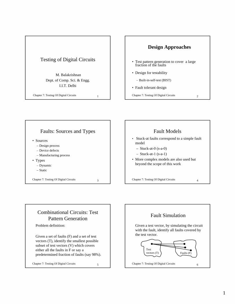
Chapter 7: Testing Of Digital Circuits 1
Testing of Digital Circuits
M. BalakrishnanDept. of Comp. Sci. & Engg.
I.I.T. Delhi
Chapter 7: Testing Of Digital Circuits 2
Design Approaches
• Test pattern generation to cover a large fraction of the faults
• Design for testability
– Built-in-self-test (BIST)
• Fault tolerant design
Chapter 7: Testing Of Digital Circuits 3
Faults: Sources and Types
• Sources– Design process– Device defects– Manufacturing process
• Types– Dynamic– Static
Chapter 7: Testing Of Digital Circuits 4
Fault Models• Stuck-at faults correspond to a simple fault
model– Stuck-at-0 (s-a-0)– Stuck-at-1 (s-a-1)
• More complex models are also used but beyond the scope of this work
Chapter 7: Testing Of Digital Circuits 5
Combinational Circuits: Test Pattern Generation
Problem definition:
Given a set of faults (F) and a set of test vectors (T), identify the smallest possible subset of test vectors (V) which covers either all the faults in F or say a predetermined fraction of faults (say 98%).
Chapter 7: Testing Of Digital Circuits 6
Fault Simulation
Given a test vector, by simulating the circuit with the fault, identify all faults covered by the test vector.
Testvectors (T) Faults (F)
2
Chapter 7: Testing Of Digital Circuits 7
Test Generation
• Given a fault, identify all the test vectors which can cover that fault.
Testvectors (T) Faults (F)
Chapter 7: Testing Of Digital Circuits 8
Limitations• Only one fault is expected to occur at one
time• Faults other than stuck-at faults are
expected to show up as stuck-at faults at some other location
• By and large fault location is not possible• These approaches are valid only for
combinational circuits
Chapter 7: Testing Of Digital Circuits 9
Typical Circuit Enhancements
• Insertion of test points• Pin amplification• Test modes• Scan chains
Chapter 7: Testing Of Digital Circuits 10
Test Generation Methods
M. BalakrishnanDept. of Comp. Sci. & Engg.
I.I.T. Delhi
Chapter 7: Testing Of Digital Circuits 11
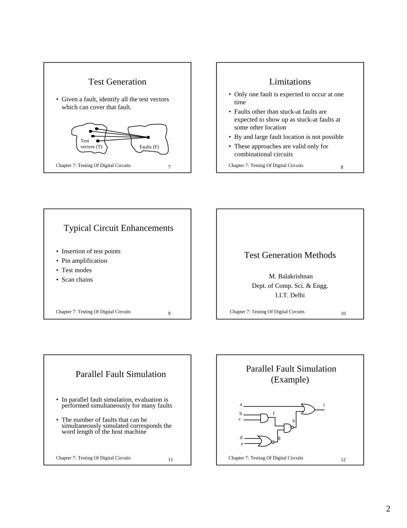
Parallel Fault Simulation
• In parallel fault simulation, evaluation is performed simultaneously for many faults
• The number of faults that can be simultaneously simulated corresponds the word length of the host machine
Chapter 7: Testing Of Digital Circuits 12
Parallel Fault Simulation (Example)
a
bc
de
f
g
h
i
3
Chapter 7: Testing Of Digital Circuits 13
Parallel Fault Simulation(Example contd.)
ff a0 a1 b0 b1 c0 c1 d0a 0 0 1 0 0 0 0 0b 1 1 1 0 1 1 1 1c 0 0 0 0 0 0 1 0d 1 1 1 1 1 1 1 0e 0 0 0 0 0 0 0 0f 0 0 0 0 0 0 1 0g 0 0 0 0 0 0 0 1h 1 1 1 1 1 1 1 1i 1 1 1 1 1 1 1 1
Chapter 7: Testing Of Digital Circuits 14
Deductive Fault Simulation
• At each of the primary inputs generate the list of faults that can be detected by the test vector
• Use these lists to generate the lists at other nodes by “appropriate” operations on these lists
Chapter 7: Testing Of Digital Circuits 15
Deductive Fault Simulation (example)
a
bc
de
f
g
h
i
La = {a1} Lb = {b0} Lc = {c1} Ld = {d0} Le = {e1}0
10
10
Lfp = Lb’ ∩ Lc = {c1}Lf = {c1, f1}Lgp = (Ld’ ∪ Le)’ = {d0}Lg = {d0, g1}Lhp’ = (Lf ∩ Lg)’, Lhp = ΦLh = {h0}Lip’ = La ∪ Lh’, Lip = {h0}Li = {h0, i0}
0
01
1
Chapter 7: Testing Of Digital Circuits 16
Deductive Fault Simulation(example contd.)
a
bc
de
f
g
h
i
La = {a1} Lb = {b0} Lc = {c0} Ld = {d0} Le = {e1}0
11
10
Lfp’ = Lb’ ∩ Lc’ = { b0, c0}Lf = {b0, c0, f0}Lgp = (Ld’ ∪ Le)’ = {d0}Lg = {d0, g1}Lhp’ = (Lf ‘∩ Lg)’Lhp = {d0,g1} , Lh = {d0,g1,h0}Lip’ = La ∪ Lh’, Lip = {d0, g1,h0}Li = {d0, g1, h0, i0}
1
01
1
Chapter 7: Testing Of Digital Circuits 17
Test Generation Methods Boolean Difference & D-Algorithm
M. BalakrishnanDept. of Comp. Sci. & Engg.
I.I.T. Delhi
Chapter 7: Testing Of Digital Circuits 18
Boolean Difference
Consider a function f of say 4 variablesf(x0, x1, x2, x3) Boolean difference of f w.r.t to xi is defined as
follows:df/dxi = f⏐xi=0 + f⏐xi=1
4
Chapter 7: Testing Of Digital Circuits 19
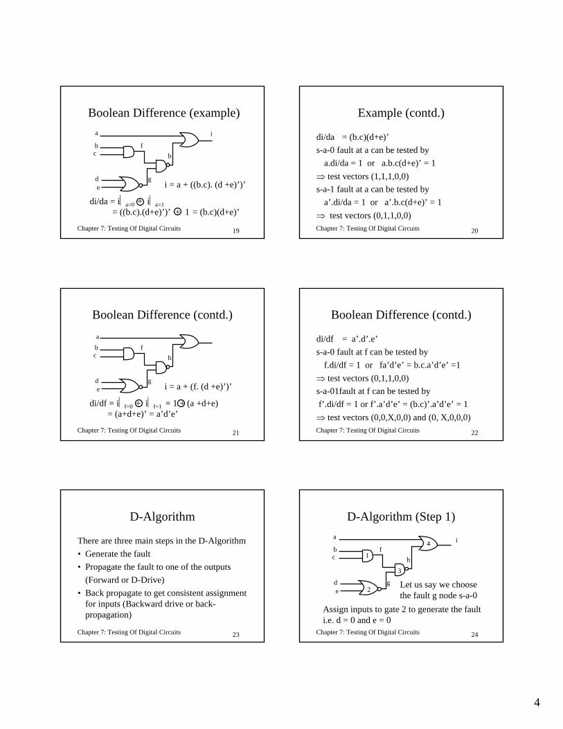
Boolean Difference (example)a
bc
de
f
g
h
i
i = a + ((b.c). (d +e)’)’
di/da = i⏐a=0 + i⏐a=1 = ((b.c).(d+e)’)’ + 1 = (b.c)(d+e)’
Chapter 7: Testing Of Digital Circuits 20
Example (contd.)
di/da = (b.c)(d+e)’s-a-0 fault at a can be tested by
a.di/da = 1 or a.b.c(d+e)’ = 1 ⇒ test vectors (1,1,1,0,0)s-a-1 fault at a can be tested by
a’.di/da = 1 or a’.b.c(d+e)’ = 1 ⇒ test vectors (0,1,1,0,0)
Chapter 7: Testing Of Digital Circuits 21
Boolean Difference (contd.)
bc
de
f
g
h
i = a + (f. (d +e)’)’
di/df = i⏐f=0 + i⏐f=1 = 1 + (a +d+e)= (a+d+e)’ = a’d’e’
a
Chapter 7: Testing Of Digital Circuits 22
Boolean Difference (contd.)
di/df = a’.d’.e’s-a-0 fault at f can be tested by
f.di/df = 1 or fa’d’e’ = b.c.a’d’e’ =1 ⇒ test vectors (0,1,1,0,0)s-a-01fault at f can be tested by f’.di/df = 1 or f’.a’d’e’ = (b.c)’.a’d’e’ = 1 ⇒ test vectors (0,0,X,0,0) and (0, X,0,0,0)
Chapter 7: Testing Of Digital Circuits 23
D-Algorithm
There are three main steps in the D-Algorithm• Generate the fault• Propagate the fault to one of the outputs
(Forward or D-Drive)• Back propagate to get consistent assignment
for inputs (Backward drive or back-propagation)
Chapter 7: Testing Of Digital Circuits 24
D-Algorithm (Step 1)
bc
de
f
g
h
Let us say we choose the fault g node s-a-0
1
2
3
4
Assign inputs to gate 2 to generate the faulti.e. d = 0 and e = 0
a i
5
Chapter 7: Testing Of Digital Circuits 25
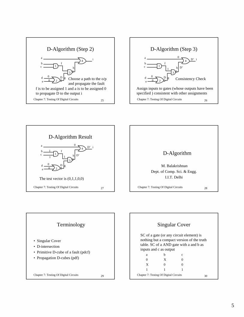
D-Algorithm (Step 2)
bc
de
f
g
h1
2
3
4a
00
D Choose a path to the o/pand propagate the fault
f is to be assigned 1 and a is to be assigned 0 to propagate D to the output i
i
Chapter 7: Testing Of Digital Circuits 26
D-Algorithm (Step 3)
bc
de
f
g
h1
2
3
4a
00
D
i
1
0
D’
D’
Consistency Check
Assign inputs to gates (whose outputs have been specified ) consistent with other assignments
Chapter 7: Testing Of Digital Circuits 27
D-Algorithm Result
bc
de
f
g
h1
2
3
4a
00
D
i
1
0
D’
D’1
1
The test vector is (0,1,1,0,0)
Chapter 7: Testing Of Digital Circuits 28
D-Algorithm
M. BalakrishnanDept. of Comp. Sci. & Engg.
I.I.T. Delhi
Chapter 7: Testing Of Digital Circuits 29
Terminology
• Singular Cover• D-intersection• Primitive D-cube of a fault (pdcf)• Propagation D-cubes (pdf)
Chapter 7: Testing Of Digital Circuits 30
Singular Cover
SC of a gate (or any circuit element) is nothing but a compact version of the truth table. SC of a AND gate with a and b as inputs and c as output
a b c0 X 0X 0 01 1 1
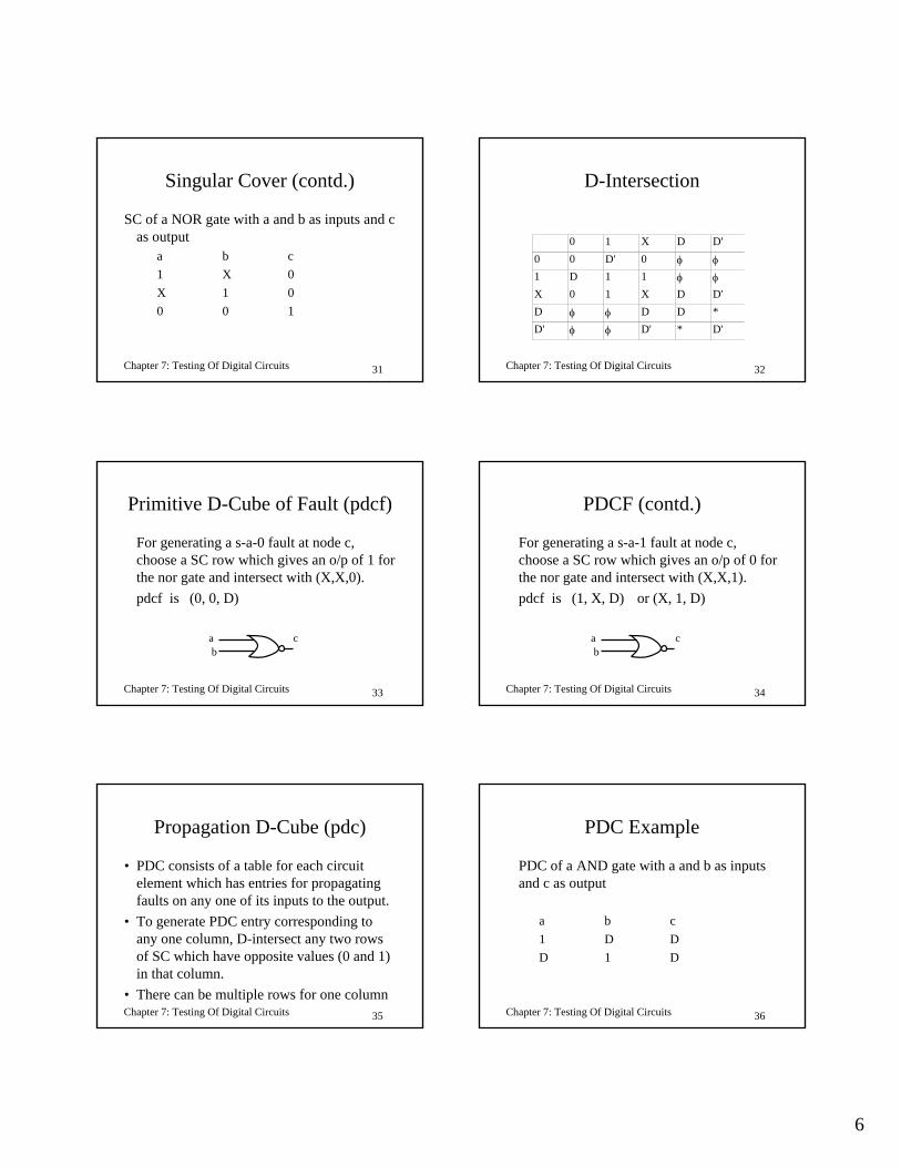
6
Chapter 7: Testing Of Digital Circuits 31
Singular Cover (contd.)
SC of a NOR gate with a and b as inputs and c as output
a b c1 X 0X 1 00 0 1
Chapter 7: Testing Of Digital Circuits 32
D-Intersection
0 1 X D D'0 0 D' 0 φ φ1 D 1 1 φ φX 0 1 X D D'D φ φ D D *D' φ φ D' * D'
Chapter 7: Testing Of Digital Circuits 33
Primitive D-Cube of Fault (pdcf)
For generating a s-a-0 fault at node c, choose a SC row which gives an o/p of 1 for the nor gate and intersect with (X,X,0).pdcf is (0, 0, D)
ab
c
Chapter 7: Testing Of Digital Circuits 34
PDCF (contd.)
For generating a s-a-1 fault at node c, choose a SC row which gives an o/p of 0 for the nor gate and intersect with (X,X,1).pdcf is (1, X, D) or (X, 1, D)
ab
c
Chapter 7: Testing Of Digital Circuits 35
Propagation D-Cube (pdc)
• PDC consists of a table for each circuit element which has entries for propagating faults on any one of its inputs to the output.
• To generate PDC entry corresponding to any one column, D-intersect any two rows of SC which have opposite values (0 and 1) in that column.
• There can be multiple rows for one column Chapter 7: Testing Of Digital Circuits 36
PDC Example
PDC of a AND gate with a and b as inputs and c as output
a b c1 D DD 1 D
7
Chapter 7: Testing Of Digital Circuits 37
PDC Example (contd.)
PDC of a NOR gate with a and b as inputs and c as output
a b c0 D D’D 0 D’
Chapter 7: Testing Of Digital Circuits 38
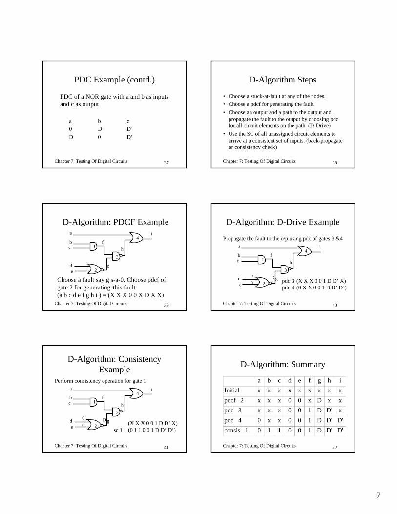
D-Algorithm Steps
• Choose a stuck-at-fault at any of the nodes.• Choose a pdcf for generating the fault. • Choose an output and a path to the output and
propagate the fault to the output by choosing pdc for all circuit elements on the path. (D-Drive)
• Use the SC of all unassigned circuit elements to arrive at a consistent set of inputs. (back-propagate or consistency check)
Chapter 7: Testing Of Digital Circuits 39
D-Algorithm: PDCF Examplea
bc
de
f
g
h
i
Choose a fault say g s-a-0. Choose pdcf of gate 2 for generating this fault(a b c d e f g h i ) = (X X X 0 0 X D X X)
1
2
3
4
Chapter 7: Testing Of Digital Circuits 40
D-Algorithm: D-Drive Example
Propagate the fault to the o/p using pdc of gates 3 &4 a
bc
de
f
g
h
i
1
2
3
4
00
D pdc 3 (X X X 0 0 1 D D’ X)pdc 4 (0 X X 0 0 1 D D’ D’)
Chapter 7: Testing Of Digital Circuits 41
D-Algorithm: Consistency Example
Perform consistency operation for gate 1 a
bc
de
f
g
h
i
1
2
3
4
00
D (X X X 0 0 1 D D’ X)sc 1 (0 1 1 0 0 1 D D’ D’)
Chapter 7: Testing Of Digital Circuits 42
D-Algorithm: Summary
a b c d e f g h iInitial x x x x x x x x xpdcf 2 x x x 0 0 x D x xpdc 3 x x x 0 0 1 D D' xpdc 4 0 x x 0 0 1 D D' D'consis. 1 0 1 1 0 0 1 D D' D'
D
8
Chapter 7: Testing Of Digital Circuits 43
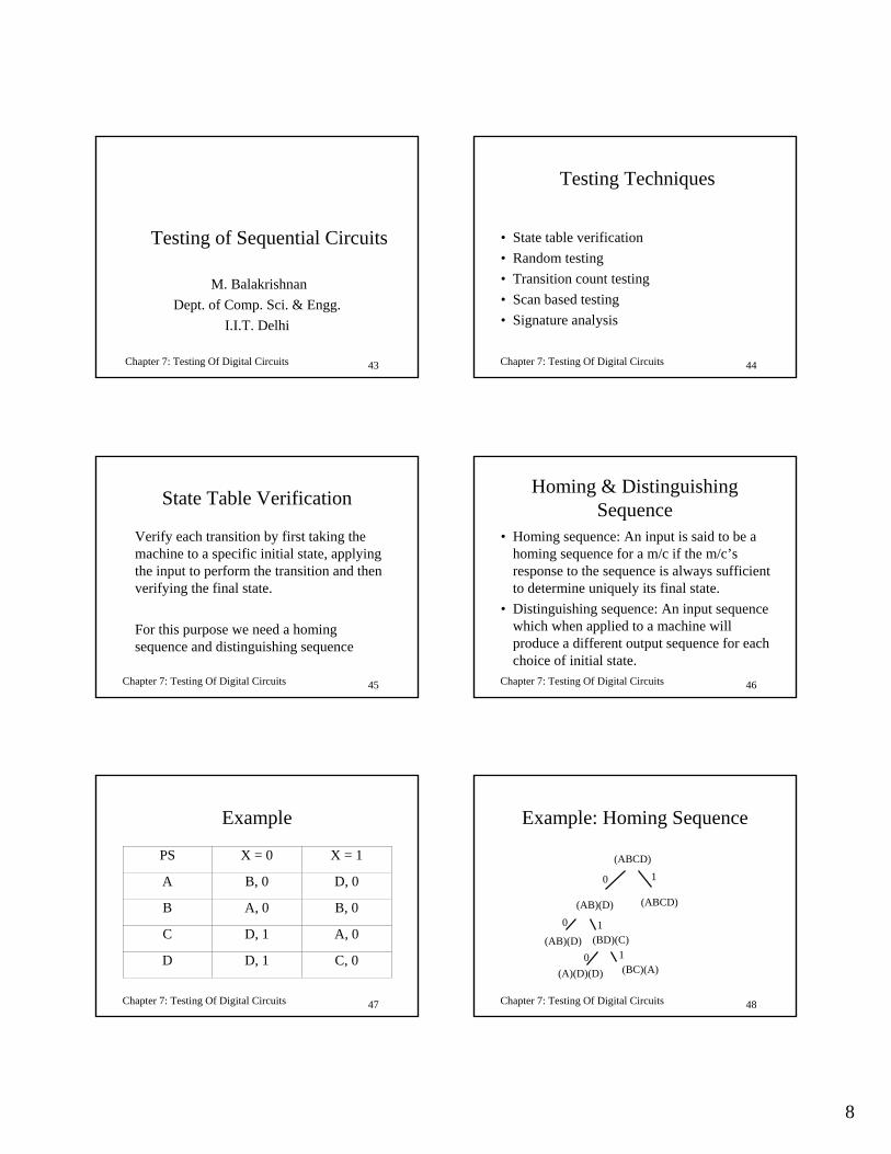
Testing of Sequential Circuits
M. BalakrishnanDept. of Comp. Sci. & Engg.
I.I.T. Delhi
Chapter 7: Testing Of Digital Circuits 44
Testing Techniques
• State table verification• Random testing• Transition count testing• Scan based testing• Signature analysis
Chapter 7: Testing Of Digital Circuits 45
State Table Verification
Verify each transition by first taking the machine to a specific initial state, applying the input to perform the transition and then verifying the final state.
For this purpose we need a homing sequence and distinguishing sequence
Chapter 7: Testing Of Digital Circuits 46
Homing & Distinguishing Sequence
• Homing sequence: An input is said to be a homing sequence for a m/c if the m/c’sresponse to the sequence is always sufficient to determine uniquely its final state.
• Distinguishing sequence: An input sequence which when applied to a machine will produce a different output sequence for each choice of initial state.
Chapter 7: Testing Of Digital Circuits 47
Example
PS X = 0 X = 1
A B, 0 D, 0
B A, 0 B, 0
C D, 1 A, 0
D D, 1 C, 0
Chapter 7: Testing Of Digital Circuits 48
Example: Homing Sequence
(ABCD)
(AB)(D) (ABCD)
(AB)(D) (BD)(C)
(A)(D)(D) (BC)(A)
0 1
0 1
0 1
9
Chapter 7: Testing Of Digital Circuits 49
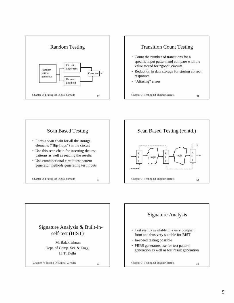
Random Testing
Randompatterngenerator
Knowngood ckt
Circuitunder test
Compare
Chapter 7: Testing Of Digital Circuits 50
Transition Count Testing
• Count the number of transitions for a specific input pattern and compare with the value stored for “good” circuits
• Reduction in data storage for storing correct responses
• “Aliasing” errors
Chapter 7: Testing Of Digital Circuits 51
Scan Based Testing
• Form a scan chain for all the storage elements (“flip-flops”) in the circuit
• Use this scan chain for inserting the test patterns as well as reading the results
• Use combinational circuit test pattern generator methods generating test inputs
Chapter 7: Testing Of Digital Circuits 52
Scan Based Testing (contd.)
logic logicReg
Reg
Reg
Chapter 7: Testing Of Digital Circuits 53
Signature Analysis & Built-in-self-test (BIST)
M. BalakrishnanDept. of Comp. Sci. & Engg.
I.I.T. Delhi
Chapter 7: Testing Of Digital Circuits 54
Signature Analysis
• Test results available in a very compact form and thus very suitable for BIST
• In-speed testing possible• PRBS generators use for test pattern
generation as well as test result generation
10
Chapter 7: Testing Of Digital Circuits 55
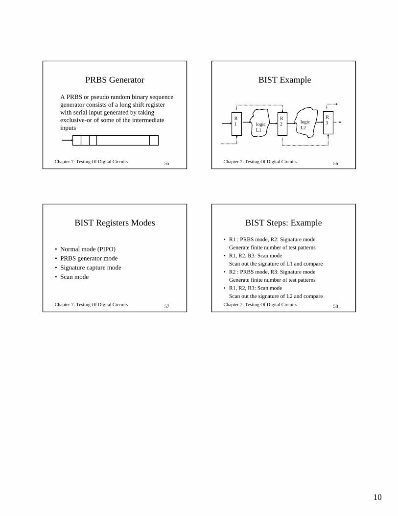
PRBS Generator
A PRBS or pseudo random binary sequence generator consists of a long shift register with serial input generated by taking exclusive-or of some of the intermediate inputs
Chapter 7: Testing Of Digital Circuits 56
BIST Example
logicL1
logicL2
R1
R2
R3
Chapter 7: Testing Of Digital Circuits 57
BIST Registers Modes
• Normal mode (PIPO)• PRBS generator mode• Signature capture mode• Scan mode
Chapter 7: Testing Of Digital Circuits 58
BIST Steps: Example
• R1 : PRBS mode, R2: Signature modeGenerate finite number of test patterns
• R1, R2, R3: Scan modeScan out the signature of L1 and compare
• R2 : PRBS mode, R3: Signature modeGenerate finite number of test patterns
• R1, R2, R3: Scan modeScan out the signature of L2 and compare
1
Chapter 8: Advanced Topics 1
Multi-Level Logic Synthesis
M. BalakrishnanDept. of Comp. Sci. & Engg.
I.I.T. Delhi
Chapter 8: Advanced Topics 2
Objective
The objective in multi-level logic synthesis is to minimize the cost under a given time-constraint (reflected as number of levels) or to perform an area-time tradeoff.
Chapter 8: Advanced Topics 3
Issues in Multi-level Logic Synthesis
The main issue is to factorise the multiple outputs (or sub-expressions in a single output function) with a view to extract the common sub-expressions.
Chapter 8: Advanced Topics 4
Common Subexpression Extraction
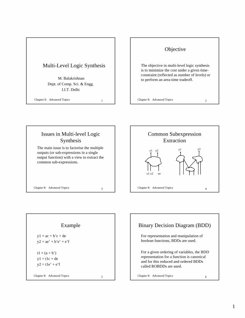
y1 y2 y1 y2
x1 x2 xn
Chapter 8: Advanced Topics 5
Example
y1 = ac + b’c + dey2 = ae’ + b’e’ + e’f
t1 = (a + b’)y1 = t1c + dey2 = t1e’ + e’f
Chapter 8: Advanced Topics 6
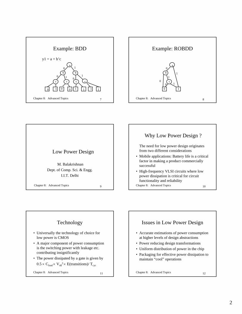
Binary Decision Diagram (BDD)
For representation and manipulation of boolean functions, BDDs are used.
For a given ordering of variables, the BDD representation for a function is canonical and for this reduced and ordered BDDs called ROBDDs are used.
2
Chapter 8: Advanced Topics 7
Example: BDD
y1 = a + b’ca
b
c c c c
b0 1
0 1 01
1 1 1 110 0 0
Chapter 8: Advanced Topics 8
Example: ROBDD
a
c
b0
01
10
1
0 1
Chapter 8: Advanced Topics 9
Low Power Design
M. BalakrishnanDept. of Comp. Sci. & Engg.
I.I.T. Delhi
Chapter 8: Advanced Topics 10
Why Low Power Design ?
The need for low power design originates from two different considerations
• Mobile applications: Battery life is a critical factor in making a product commercially successful
• High-frequency VLSI circuits where low power dissipation is critical for circuit functionality and reliability
Chapter 8: Advanced Topics 11
Technology
• Universally the technology of choice for low power is CMOS
• A major component of power consumption is the switching power with leakage etc. contributing insignificantly
• The power dissipated by a gate is given by0.5 × Cload × Vdd
2 × E(transitions)/ Tcyc
Chapter 8: Advanced Topics 12
Issues in Low Power Design
• Accurate estimations of power consumption at higher levels of design abstractions
• Power reducing design transformations• Uniform distribution of power in the chip• Packaging for effective power dissipation to
maintain “cool” operations
3
Chapter 8: Advanced Topics 13
Power Estimation
Power can be estimated by simulating the behavior at different levels.
• Transistor level• Gate level• RTL module level• Software power estimation• Architecture level
Chapter 8: Advanced Topics 14
Design Transformations
• Critical path reduction• Reducing the number of operations• Reducing the transition activity• Reducing the interconnect capacitance• Operation substitution• Bit-width optimization
Chapter 8: Advanced Topics 15
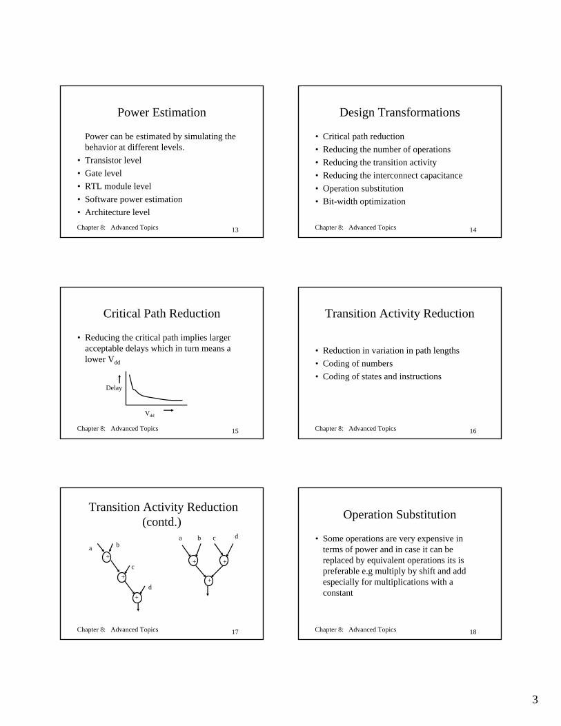
Critical Path Reduction
• Reducing the critical path implies larger acceptable delays which in turn means a lower Vdd
Vdd
Delay
Chapter 8: Advanced Topics 16
Transition Activity Reduction
• Reduction in variation in path lengths• Coding of numbers• Coding of states and instructions
Chapter 8: Advanced Topics 17
Transition Activity Reduction (contd.)
+
+
+
+ +
+
a b
c
d
a b c d
Chapter 8: Advanced Topics 18
Operation Substitution
• Some operations are very expensive in terms of power and in case it can be replaced by equivalent operations its is preferable e.g multiply by shift and add especially for multiplications with a constant
4
Chapter 8: Advanced Topics 19
Behavioral Synthesis
M. BalakrishnanDept. of Comp. Sci. & Engg.
I.I.T. Delhi
Chapter 8: Advanced Topics 20
Why Behavioral Synthesis ?
There is urgent need for pushing up the abstraction level at which the design can start. The reasons for this are:
• As the complexity increases, this is the only way to reduce the design turn around time
• An algorithmic description of the functionality is far easier to write than designing hardware
Chapter 8: Advanced Topics 21
Steps in Behavioral Synthesis
• Data path synthesis– Scheduling– Resource allocation (where resources include
functional units, storage units, buses and interconnects)
– Resource binding• Control synthesis• Clock synthesis
Chapter 8: Advanced Topics 22
Scheduling
• Assigning operations to control steps• This phase has a lot of influence on
resource allocation as what can be done concurrently depends upon the resource availability
• Complexity arises due to the range of available functional units (pipelined, multi-functional, multi-cycle etc.)
Chapter 8: Advanced Topics 23
Resource Allocation• Typically manual but automating allocation
algorithms are also available• FU allocation: Complexity due to the range
of operators i.e. Multi-cycle, multi-function, pipelined, mixed speed operators for the same operation
• Storage allocation: e.g. Registers, Memory units, Multi-port memories, Register files
Chapter 8: Advanced Topics 24
Resource Binding
• Examples of binding to be carried out are– Operation-operator binding– Variable-storage unit binding– Transfer-interconnect/bus binding
• Binding has considerable influence on number of interconnects
• Scheduling also influences binding
5
Chapter 8: Advanced Topics 25
Control & Clock Synthesis
• Generate a state machine from the control flow of the algorithm
• Identify the control and status signals• Synthesize the control part• Analyze the critical path to decide on the
clock period
Chapter 8: Advanced Topics 26
Objectives in Behavioral Synthesis
• Minimize delay time or maximize performance
• Minimize cost or area• Meet constraints on area and/or
performance
Chapter 8: Advanced Topics 27
Recent Trends in Behavioral Synthesis
• Incorporate testability conditions in synthesis
• Incorporate power minimization as part of the design objective i.e. explore the design space from power considerations
Chapter 8: Advanced Topics 28
System Level Design & Modeling
M. BalakrishnanDept. of Comp. Sci. & Engg.
I.I.T. Delhi
Chapter 8: Advanced Topics 29
Issues in System Level Design
• Specification– At different levels of design
• Verification– Formal verification– Simulation
• Partitioning and estimation• Synthesis
Chapter 8: Advanced Topics 30
Characteristics of Current Systems
• One (or more) processors– Heterogeneous processor set
• IP cores for critical parts of the application• Mixed hardware/software implementation• Many systems are real-time reactive
systems
6
Chapter 8: Advanced Topics 31
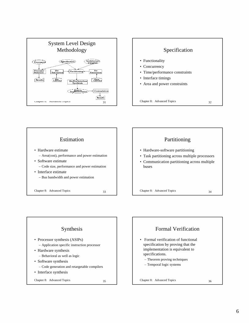
System Level Design Methodology
Chapter 8: Advanced Topics 32
Specification
• Functionality• Concurrency• Time/performance constraints• Interface timings• Area and power constraints
Chapter 8: Advanced Topics 33
Estimation
• Hardware estimate– Area(cost), performance and power estimation
• Software estimate– Code size, performance and power estimation
• Interface estimate– Bus bandwidth and power estimation
Chapter 8: Advanced Topics 34
Partitioning
• Hardware-software partitioning• Task partitioning across multiple processors• Communication partitioning across multiple
buses
Chapter 8: Advanced Topics 35
Synthesis
• Processor synthesis (ASIPs)– Application specific instruction processor
• Hardware synthesis– Behavioral as well as logic
• Software synthesis– Code generation and retargetable compilers
• Interface synthesis
Chapter 8: Advanced Topics 36
Formal Verification
• Formal verification of functional specification by proving that the implementation is equivalent to specifications.– Theorem proving techniques– Temporal logic systems
7
Chapter 8: Advanced Topics 37
SimulationVerification by simulation though expensive but is the only widely used technique.
• Cosimulation e.g. C and VHDL• Test stimulus generation
![Public Key Certification and Revocationalfchen/teaching/cs134-2019...Public Key Certification and Revocation [lecture slides are adapted from previous slides by Prof. Gene Tsudik]](https://img.pdfslide.net/doc/110x75/5f0635157e708231d416d58d/public-key-certification-and-revocation-alfchenteachingcs134-2019-public-key.jpg)