Embed Size (px)
Citation preview
Programmable logic and Programmable logic and FPGAFPGA
CPU ArchitectureCPU Architecture
Serge KarabchevskySerge Karabchevsky
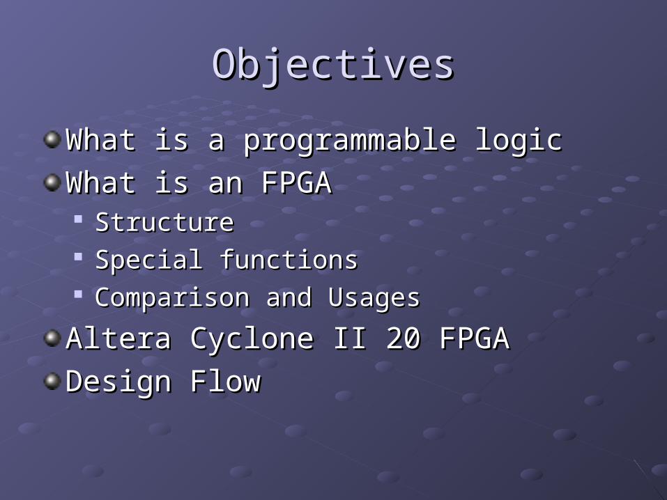
ObjectivesObjectives
What is a programmable logicWhat is a programmable logic
What is an FPGAWhat is an FPGA StructureStructure Special functionsSpecial functions Comparison and UsagesComparison and Usages
Altera Cyclone II 20 FPGAAltera Cyclone II 20 FPGA
Design FlowDesign Flow
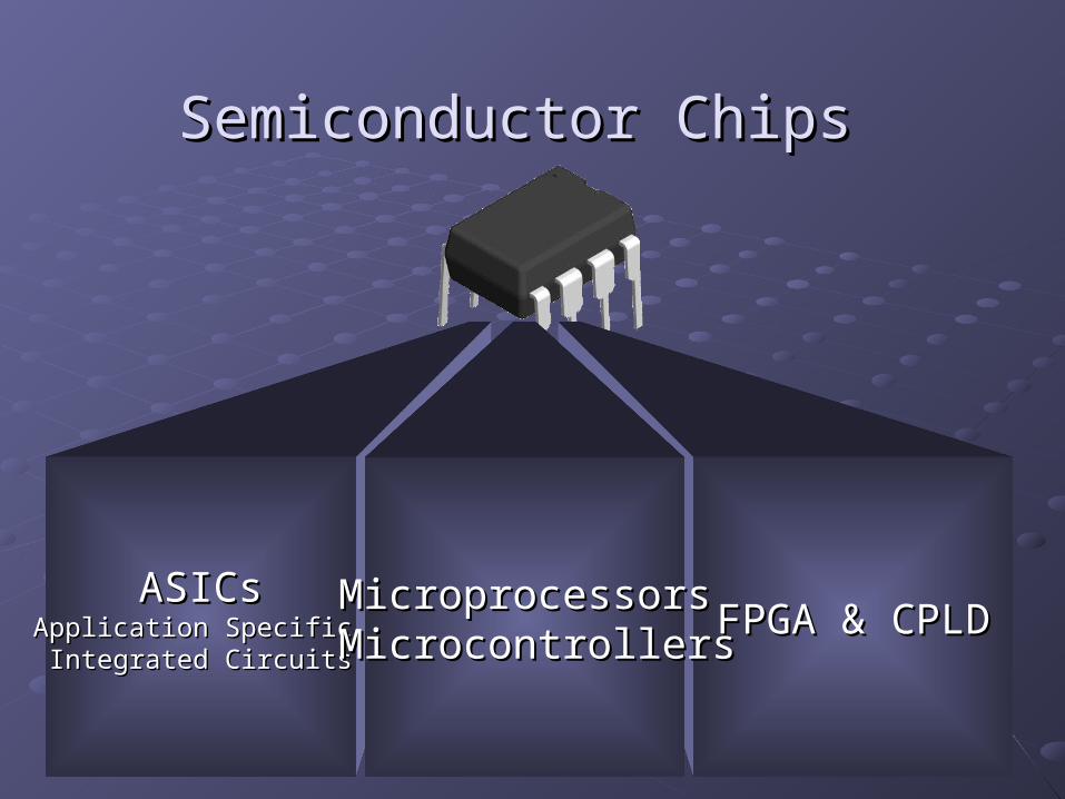
Semiconductor Chips Semiconductor Chips
FPGA & CPLDFPGA & CPLDASICsASICs
Application Specific Application Specific Integrated CircuitsIntegrated Circuits
MicroprocessorsMicroprocessors MicrocontrollersMicrocontrollers
Programmable logicProgrammable logic
An integrated circuit that can be An integrated circuit that can be programmed/reprogrammed with a digital programmed/reprogrammed with a digital logic of a curtain level.logic of a curtain level.
Started at late 70s and constantly growingStarted at late 70s and constantly growing
Now available of up to approximately 700K Now available of up to approximately 700K Flip-Flops in a single chip.Flip-Flops in a single chip.
AdvantagesAdvantages
Short Development timeShort Development timeReconfigurableReconfigurableSaves board spaceSaves board spaceFlexible to changesFlexible to changesNo need for ASIC expensive design and No need for ASIC expensive design and productionproductionFast time to marketFast time to marketBugs can be fixed easilyBugs can be fixed easilyOf the shelf solutions are availableOf the shelf solutions are available
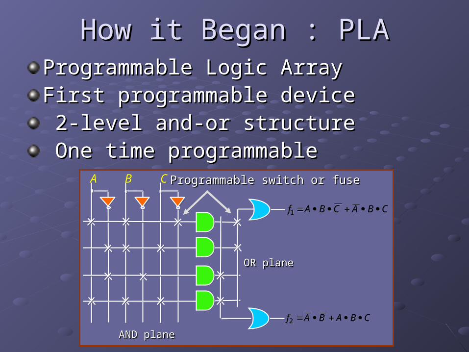
How it Began : PLAHow it Began : PLA
AA BB CC
CBACBAf 1 CBACBAf 1
CBABAf 2 CBABAf 2
AND planeAND planeAND planeAND plane
Programmable switch or fuseProgrammable switch or fuseProgrammable switch or fuseProgrammable switch or fuse
OR planeOR planeOR planeOR plane
Programmable Logic ArrayProgrammable Logic ArrayFirst programmable deviceFirst programmable device 2-level and-or structure2-level and-or structure One time programmableOne time programmable
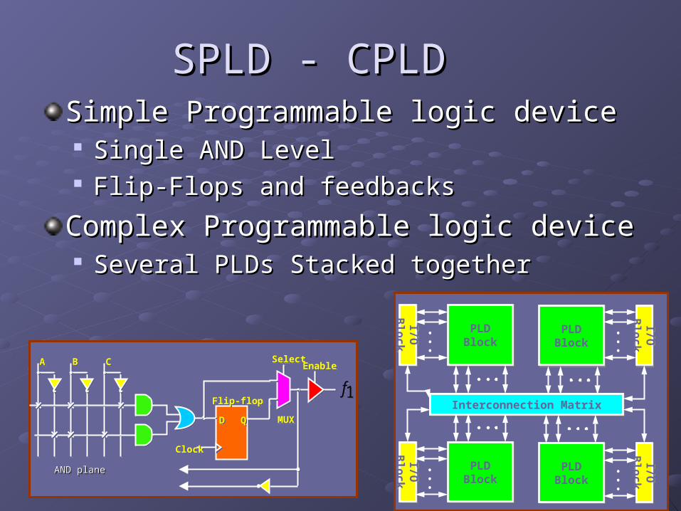
SPLD - CPLDSPLD - CPLDSimple Programmable logic deviceSimple Programmable logic device Single AND LevelSingle AND Level Flip-Flops and feedbacksFlip-Flops and feedbacks
Complex Programmable logic deviceComplex Programmable logic device Several PLDs Stacked togetherSeveral PLDs Stacked together
AA BB CC
Flip-flopFlip-flop
SelectSelectEnableEnable
DD QQ
ClockClock
AND planeAND planeAND planeAND plane
MUXMUX
1f1f
PLDBlockPLD
BlockPLD
BlockPLD
Block
Interconnection MatrixInterconnection Matrix
I/O B
loc
kI/O
Blo
ck
I/O B
loc
kI/O
Blo
ck
PLDBlockPLD
BlockPLD
BlockPLD
Block
I/O B
loc
kI/O
Blo
ck
I/O B
loc
kI/O
Blo
ck
• • •
Interconnection MatrixInterconnection Matrix
• • •
• • •
• • •
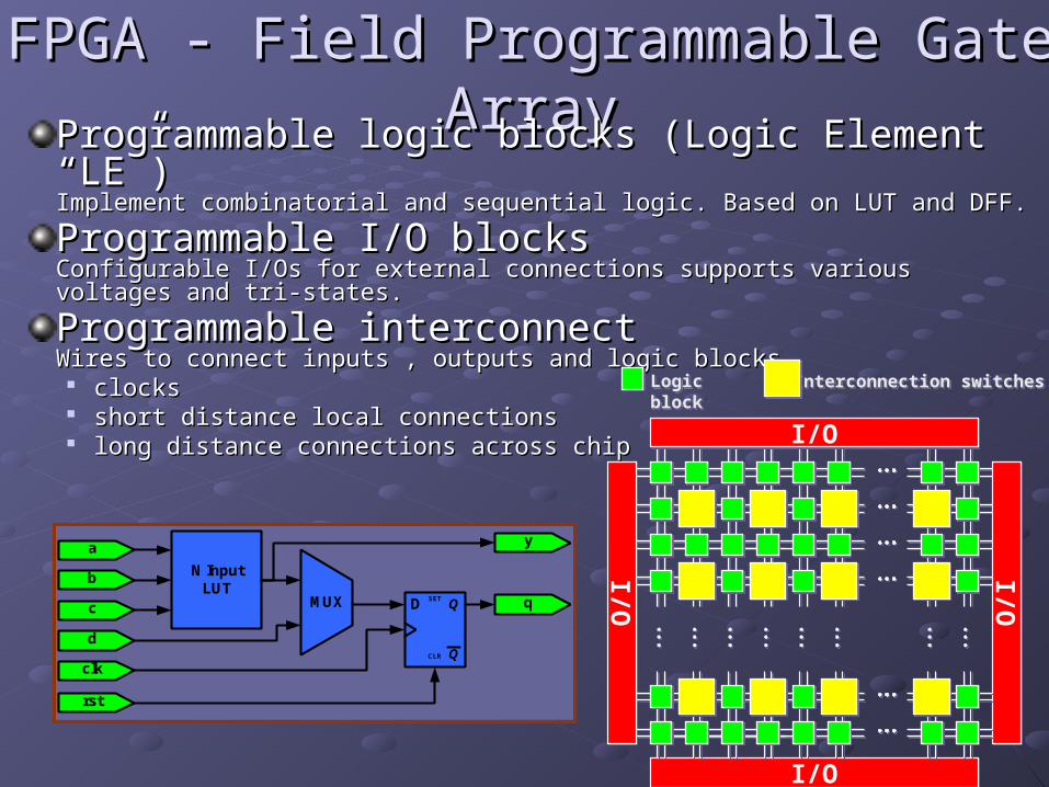
FPGA - Field Programmable Gate ArrayFPGA - Field Programmable Gate ArrayProgrammable logic blocks (Logic Element “LE”)Programmable logic blocks (Logic Element “LE”)Implement combinatorial and sequential logic. Based on LUT and DFF. Implement combinatorial and sequential logic. Based on LUT and DFF.
Programmable I/O blocksProgrammable I/O blocks Configurable I/Os for external connections supports various voltages and tri-states.Configurable I/Os for external connections supports various voltages and tri-states.
Programmable interconnectProgrammable interconnectWires to connect inputs , outputs and logic blocks. Wires to connect inputs , outputs and logic blocks.
clocksclocks short distance local connectionsshort distance local connections long distance connections across chiplong distance connections across chip
I/OI/O
I/OI/O
Logic blockLogic block
Interconnection switchesInterconnection switches
I/OI/O
I/OI/O
N Input LUT
Q
QSET
CLR
DMUX
d
a
clk
rst
y
q
b
c
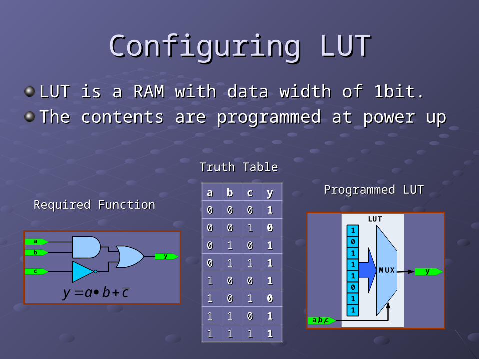
Configuring LUTConfiguring LUT
a
b
c
y
y a b c
aa bb cc yy
00 00 00 11
00 00 11 00
00 11 00 11
00 11 11 11
11 00 00 11
11 00 11 00
11 11 00 11
11 11 11 11
Required FunctionRequired Function
Truth TableTruth Table
Programmed LUTProgrammed LUT
1
0
1
1
1
0
1
1
MUX y
a,b,c
LUT
LUT is a RAM with data width of 1bit.LUT is a RAM with data width of 1bit.
The contents are programmed at power upThe contents are programmed at power up
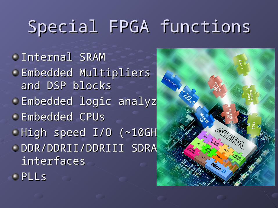
Special FPGA functionsSpecial FPGA functions
Internal SRAMInternal SRAM
Embedded Multipliers Embedded Multipliers and DSP blocksand DSP blocks
Embedded logic analyzerEmbedded logic analyzer
Embedded CPUsEmbedded CPUs
High speed I/O (~10GHz)High speed I/O (~10GHz)
DDR/DDRII/DDRIII SDRAM DDR/DDRII/DDRIII SDRAM interfacesinterfaces
PLLsPLLs
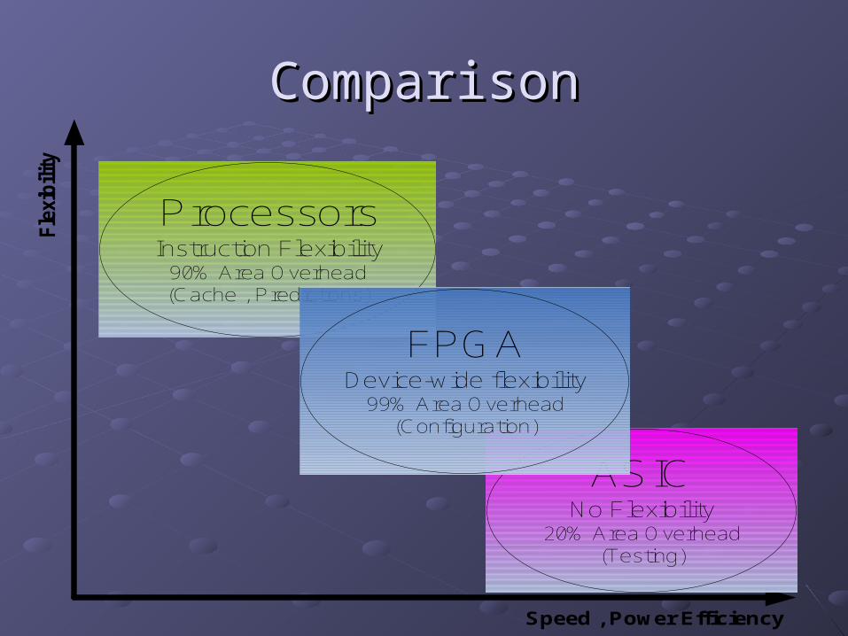
ComparisonComparisonFl
exib
ility
Speed , Power Efficiency
ProcessorsInstruction Flexibility
90% Area Overhead(Cache , Predictions)
ASICNo Flexibility
20% Area Overhead(Testing)
FPGADevice-wide flexibility
99% Area Overhead(Configuration)
UsagesUsages
Digital designs where ASIC is not Digital designs where ASIC is not commercialcommercial
Reconfigurable systemsReconfigurable systems
Upgradeable systemsUpgradeable systems
ASIC prototyping and emulationASIC prototyping and emulation
EducationEducation
ManufacturersManufacturers
XilinxXilinx
AlteraAltera
LatticeLattice
ActelActel
We will work with Altera FPGAsWe will work with Altera FPGAs
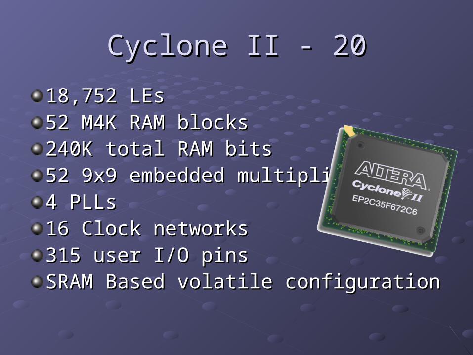
Cyclone II - 20Cyclone II - 20
18,752 LEs 18,752 LEs 52 M4K RAM blocks 52 M4K RAM blocks 240K total RAM bits 240K total RAM bits 52 9x9 embedded multipliers 52 9x9 embedded multipliers 4 PLLs 4 PLLs 16 Clock networks16 Clock networks315 user I/O pins 315 user I/O pins SRAM Based volatile configurationSRAM Based volatile configuration
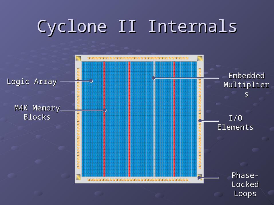
Cyclone II InternalsCyclone II Internals
Logic ArrayLogic Array
M4K MemoryM4K MemoryBlocksBlocks
EmbeddedEmbeddedMultipliersMultipliers
Phase-LockedPhase-LockedLoopsLoops
I/OI/OElementsElements
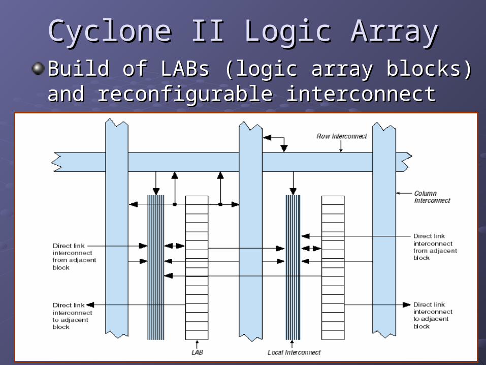
Cyclone II Logic ArrayCyclone II Logic ArrayBuild of LABs (logic array blocks) and Build of LABs (logic array blocks) and reconfigurable interconnect reconfigurable interconnect
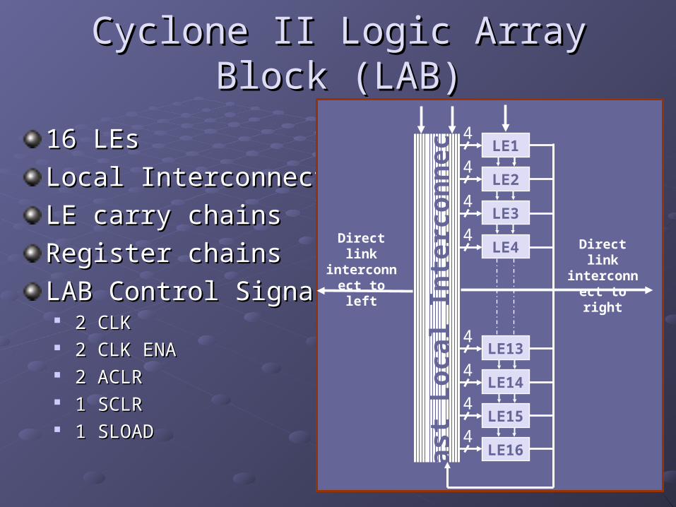
Cyclone II Logic Array Block (LAB)Cyclone II Logic Array Block (LAB)
16 LEs16 LEs
Local InterconnectLocal Interconnect
LE carry chainsLE carry chains
Register chainsRegister chains
LAB Control SignalsLAB Control Signals 2 CLK2 CLK 2 CLK ENA2 CLK ENA 2 ACLR2 ACLR 1 SCLR1 SCLR 1 SLOAD1 SLOAD
LE1
LE2
LE3
LE4
LE13
LE14
LE16
LE15
4
4
4
4
4
4
4
4Fas
t L
oca
l In
terc
on
nec
t
Direct link interconnec
t to left
Direct link interconnec
t to right
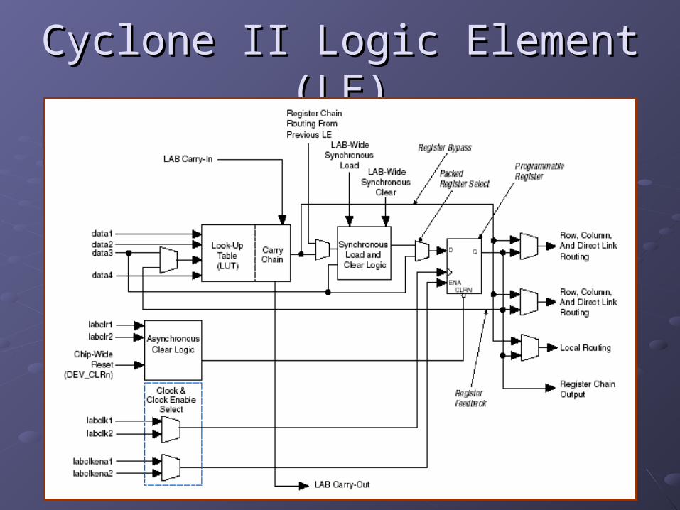
Cyclone II Logic Element (LE)Cyclone II Logic Element (LE)
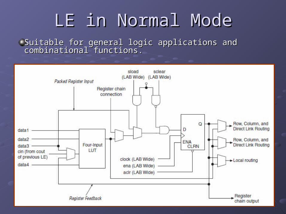
LE in Normal ModeLE in Normal ModeSuitable for general logic applications and combinational Suitable for general logic applications and combinational functions.functions.
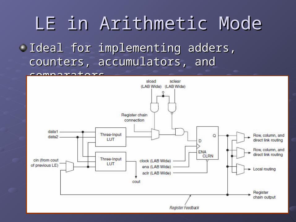
LE in Arithmetic ModeLE in Arithmetic ModeIdeal for implementing adders, counters, Ideal for implementing adders, counters, accumulators, and comparators.accumulators, and comparators.
Cyclone II I/O FeaturesCyclone II I/O Features
In/Out/Tri-stateIn/Out/Tri-stateDifferent Voltages and I/O StandardsDifferent Voltages and I/O StandardsFlip-flop optionFlip-flop optionPull-up resistorsPull-up resistorsDDR interfaceDDR interfaceSeries resistorsSeries resistorsBus keeperBus keeperDrive strength controlDrive strength controlSlew rate controlSlew rate controlSingle ended/differentialSingle ended/differential
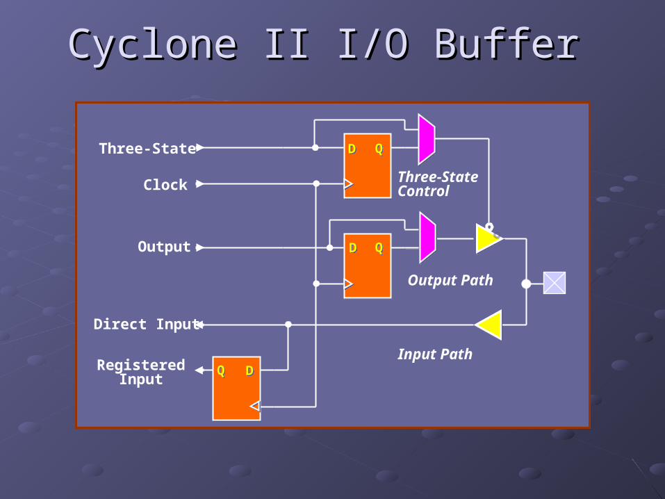
Cyclone II I/O BufferCyclone II I/O Buffer
DDQQ
DD QQ
DD QQ
Three-StateControl
Output Path
Input Path
Three-State
Output
Clock
Direct Input
Registered Input
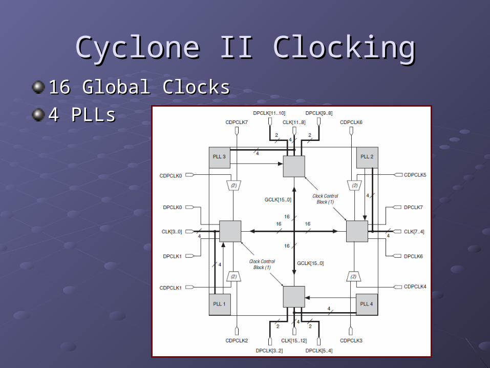
Cyclone II ClockingCyclone II Clocking16 Global Clocks16 Global Clocks
4 PLLs4 PLLs
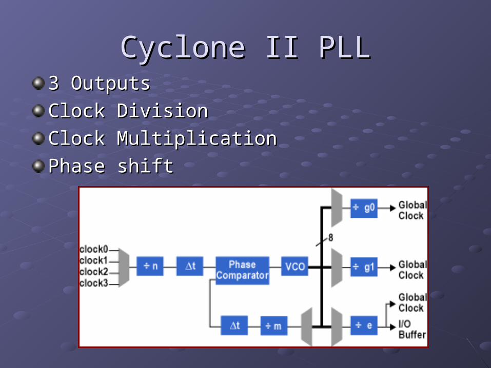
Cyclone II PLLCyclone II PLL3 Outputs3 Outputs
Clock DivisionClock Division
Clock MultiplicationClock Multiplication
Phase shiftPhase shift
MemoryMemory
True Dual port RAM/ROM with dual clockTrue Dual port RAM/ROM with dual clock
Variable data width Variable data width 4K×1, 2K×2, 1K×4, 512×8, 512×9, 256×16, 256×184K×1, 2K×2, 1K×4, 512×8, 512×9, 256×16, 256×18 128×32, 128×36 (not available in true dual-port mode)128×32, 128×36 (not available in true dual-port mode)
Input data and address are registeredInput data and address are registered 1 Clock Write latency 1 Clock Write latency
Output data can be registeredOutput data can be registered Read latency of 1 or 2 clocksRead latency of 1 or 2 clocks
Byte EnableByte Enable
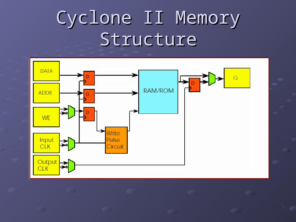
Cyclone II Memory StructureCyclone II Memory Structure
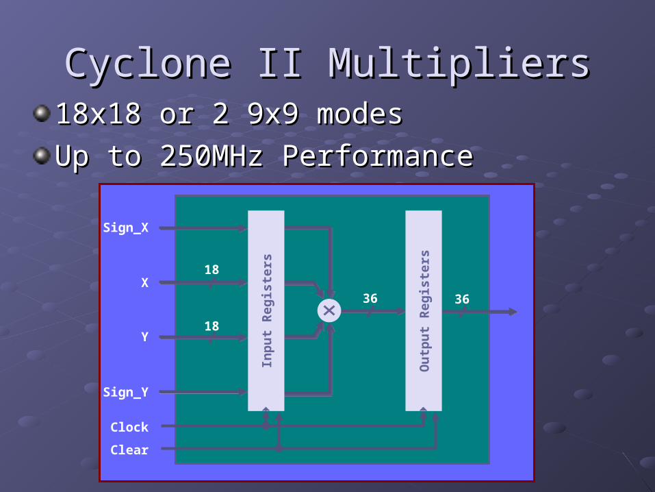
Cyclone II MultipliersCyclone II Multipliers18x18 or 2 9x9 modes 18x18 or 2 9x9 modes
Up to 250MHz PerformanceUp to 250MHz Performance
18
Sign_X
18X
Y
Sign_Y
Inp
ut
Reg
iste
rs
36
Clock
Clear
36
Ou
tpu
t R
eg
iste
rs
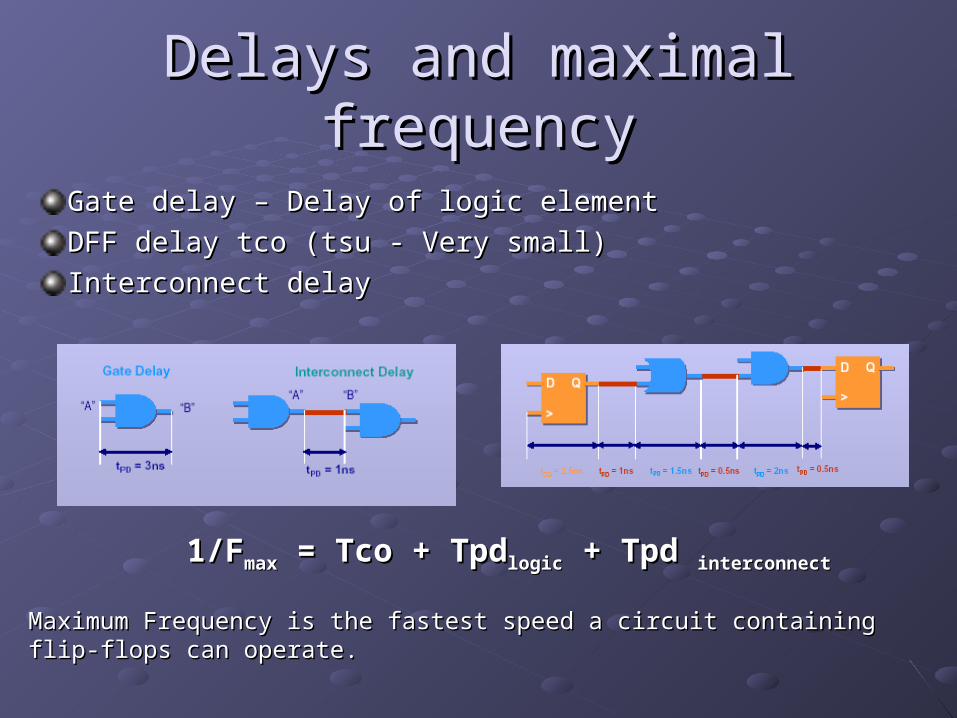
Delays and maximal frequencyDelays and maximal frequency
Gate delay – Delay of logic element Gate delay – Delay of logic element
DFF delay tco (tsu - Very small)DFF delay tco (tsu - Very small)
Interconnect delay Interconnect delay
Maximum FrequencyMaximum Frequency isis the fastest speed a circuit containing flip-flops can operate.the fastest speed a circuit containing flip-flops can operate.
1/F1/Fmaxmax = Tco + Tpd = Tco + Tpdlogiclogic + Tpd + Tpd interconnectinterconnect
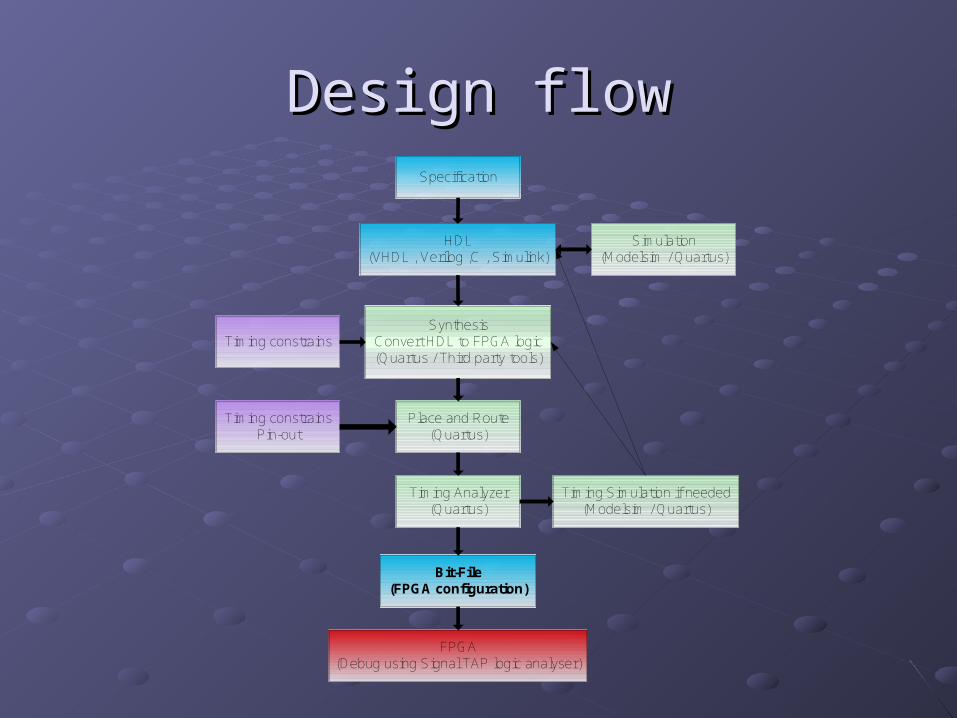
Design flowDesign flowSpecification
HDL(VHDL , Verilog ,C , Simulink)
Simulation(Modelsim / Quartus)
SynthesisConvert HDL to FPGA logic(Quartus / Third party tools)
Place and Route(Quartus)
Bit-File(FPGA configuration)
Timing constrains
FPGA(Debug using Signal TAP logic analyser)
Timing Simulation if needed(Modelsim / Quartus)
Timing Analyzer(Quartus)
Timing constrains Pin-out
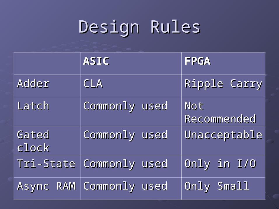
Design RulesDesign Rules
ASICASIC FPGAFPGA
AdderAdder CLACLA Ripple CarryRipple Carry
LatchLatch Commonly usedCommonly used Not Not RecommendedRecommended
Gated clockGated clock Commonly usedCommonly used UnacceptableUnacceptable
Tri-StateTri-State Commonly usedCommonly used Only in I/OOnly in I/O
Async RAMAsync RAM Commonly usedCommonly used Only SmallOnly Small

Any questions?