Embed Size (px)
Citation preview
NRC-EVLA Memo# 014 1
National Research CouncilCanada
Conseil national de recherchesCanada
Refined EVLA WIDAR Correlator Architecture
NRC-EVLA Memo# 014
Brent Carlson, October 2, 2001
National Research Council of Canada,Herzberg Institute of Astrophysics
NRC-EVLA Memo# 014 2
National Research CouncilCanada
Conseil national de recherchesCanada
ABSTRACT
This memo is a technical blueprint for further development of the WIDARcorrelator for the EVLA. This document is not intended for the casual reader,and the assumption is made that the reader is familiar with all of the precedingmemos in this series, and with correlator signal processing. In some sections,particularly concerning the Baseline Board, many functional and performancedetails are included to provide a concrete baseline plan for implementation.This helps to establish a high level of confidence that some of the more‘exotic’ correlator functions can indeed be realized. In other sections, lessdetail is provided since functionality is reasonably straightforward.
The concepts presented in this document were developed over a period ofabout two years with valuable input and feedback from many NRAOengineers, scientists, and users during several meetings. Nothing in thisdocument is ‘etched in stone’, but it presents at least one coherent plan so thatcorrelator development can proceed to its next phase of implementation.
NRC-EVLA Memo# 014 3
National Research CouncilCanada
Conseil national de recherchesCanada
Table of Contents1 EXECUTIVE SUMMARY OF CORRELATOR CAPABILITIES ............................................. 11
2 SYSTEM OVERVIEW..................................................................................................................... 12
2.1 FLEXIBILITIES ................................................................................................................................. 14
3 STATION BOARD ........................................................................................................................... 16
3.1 FOTS RX MODULE(S) ..................................................................................................................... 173.2 DATA PATH SWITCH ....................................................................................................................... 183.3 COARSE DELAY MODULE ............................................................................................................... 193.4 FINE DELAY CONTROLLER.............................................................................................................. 193.5 WIDEBAND AUTOCORRELATOR ...................................................................................................... 203.6 DELAY GENERATOR........................................................................................................................ 203.7 FIR FILTER BANKS ......................................................................................................................... 21
3.7.1 Sub-band Multi-beaming ...................................................................................................... 223.7.2 7-bit Requantization and Correlation................................................................................... 24
3.8 OUTPUT CROSS-BAR SWITCH AND PULSAR TIMING ........................................................................ 253.9 FORMATTING AND TIMING............................................................................................................... 253.10 MISCELLANEOUS FUNCTIONS..................................................................................................... 26
4 BASELINE BOARD......................................................................................................................... 27
4.1 RECIRCULATION CONTROLLER ....................................................................................................... 304.1.1 Signal Descriptions............................................................................................................... 31
4.1.1.1 Inputs from Station Boards ............................................................................................................. 314.1.1.2 Outputs to Correlator Chips ............................................................................................................ 35
4.1.2 Simplified Block Diagram..................................................................................................... 384.1.3 Input Timing and Synchronization........................................................................................ 404.1.4 Recirculation ........................................................................................................................ 42
4.1.4.1 Timestamps ..................................................................................................................................... 444.1.4.2 Wide-band Recirculation ................................................................................................................ 47
4.1.5 Control and Synchronization Issues ..................................................................................... 484.1.5.1 Recirculation Real-Time Control .................................................................................................... 484.1.5.2 Normal Dumping Real-Time Control ............................................................................................. 504.1.5.3 Pulsar Phase Binning Real-Time Control........................................................................................ 504.1.5.4 Pulsar Phase Binning and Recirculation Real-Time Control .......................................................... 51
4.2 CORRELATOR CHIP ......................................................................................................................... 524.2.1 Simplified Functional Description........................................................................................ 524.2.2 Detailed Functional Description .......................................................................................... 54
4.2.2.1 Black-Box Correlator Chip Diagram............................................................................................... 554.2.2.2 Correlator Chip Block Diagram ...................................................................................................... 58
4.2.2.2.1 Dump Data Capture/Generator ............................................................................................. 594.2.2.2.2 SID/SBID/BBID Capture ..................................................................................................... 594.2.2.2.3 VLBI Mode Phase Modifier and Vernier Delay Generator .................................................. 594.2.2.2.4 Readout Controller/LTA Interface........................................................................................ 604.2.2.2.5 4X CCQ Lag Correlator Array ............................................................................................. 61
4.3 LTA CONTROLLER ......................................................................................................................... 654.3.1 Black-Box Description and the Front Panel Data Port Interface ........................................ 65
4.3.1.1 Output Data Frame Formats ............................................................................................................ 694.3.2 Detailed LTA Controller Functional Description................................................................. 71
4.4 FPDP SCHEDULER FPGA ............................................................................................................... 774.5 BASELINE BOARD PHYSICAL LAYOUT ............................................................................................ 77
5 PHASING BOARD........................................................................................................................... 84
5.1 4-STATION MIXER AND 1ST STAGE ADDER ...................................................................................... 85
NRC-EVLA Memo# 014 4
National Research CouncilCanada
Conseil national de recherchesCanada
5.2 2ND STAGE SUB-ARRAY ADDER....................................................................................................... 865.3 HILBERT FIR................................................................................................................................... 865.4 SUB-SUB-BAND FIR FILTER BANK ................................................................................................. 875.5 OUTPUT SWITCH AND FORMATTING .............................................................................................. 875.6 ERROR DETECTION ......................................................................................................................... 87
6 MISCELLANEOUS MODULES..................................................................................................... 89
6.1 SUB-BAND DISTRIBUTOR BACKPLANE ............................................................................................ 896.1.1 MDR-80 Connector Pin Assignments ................................................................................... 90
6.2 STATION DATA FANOUT BOARD ..................................................................................................... 926.3 BASELINE ENTRY BACKPLANE........................................................................................................ 946.4 PHASING BOARD ENTRY BACKPLANE............................................................................................. 956.5 TIMECODE GENERATOR BOX ...................................................................................................... 966.6 OTHER MODULES............................................................................................................................ 96
7 SYSTEM DESIGN............................................................................................................................ 98
7.1 SUB-RACK AND RACK DESIGN........................................................................................................ 987.2 REMOTE POWER CONTROL AND MONITORING.............................................................................. 1017.3 CORRELATOR FLOOR PLAN........................................................................................................... 1027.4 CORRELATOR COMPUTING............................................................................................................ 105
7.4.1 Hardware Configuration .................................................................................................... 1057.4.2 Software Configuration ...................................................................................................... 107
8 REFERENCES................................................................................................................................ 108
NRC-EVLA Memo# 014 5
National Research CouncilCanada
Conseil national de recherchesCanada
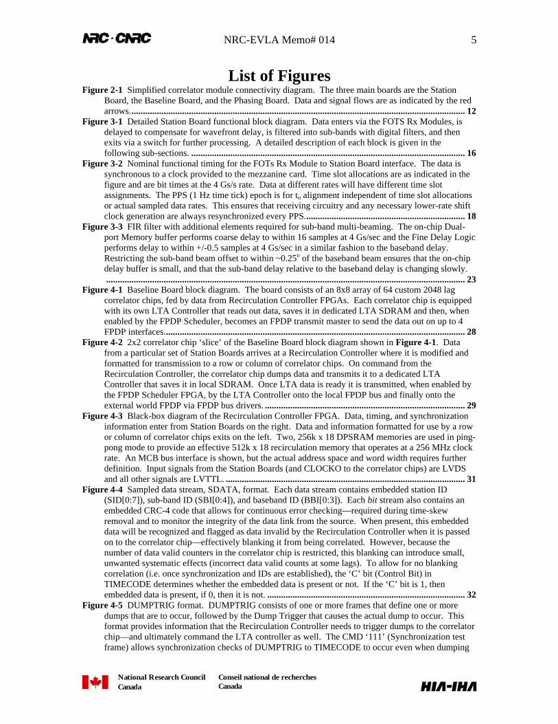
List of FiguresFigure 2-1 Simplified correlator module connectivity diagram. The three main boards are the Station
Board, the Baseline Board, and the Phasing Board. Data and signal flows are as indicated by the redarrows.................................................................................................................................................. 12
Figure 3-1 Detailed Station Board functional block diagram. Data enters via the FOTS Rx Modules, isdelayed to compensate for wavefront delay, is filtered into sub-bands with digital filters, and thenexits via a switch for further processing. A detailed description of each block is given in thefollowing sub-sections. ....................................................................................................................... 16
Figure 3-2 Nominal functional timing for the FOTs Rx Module to Station Board interface. The data issynchronous to a clock provided to the mezzanine card. Time slot allocations are as indicated in thefigure and are bit times at the 4 Gs/s rate. Data at different rates will have different time slotassignments. The PPS (1 Hz time tick) epoch is for to alignment independent of time slot allocationsor actual sampled data rates. This ensures that receiving circuitry and any necessary lower-rate shiftclock generation are always resynchronized every PPS...................................................................... 18
Figure 3-3 FIR filter with additional elements required for sub-band multi-beaming. The on-chip Dual-port Memory buffer performs coarse delay to within 16 samples at 4 Gs/sec and the Fine Delay Logicperforms delay to within +/-0.5 samples at 4 Gs/sec in a similar fashion to the baseband delay.Restricting the sub-band beam offset to within ~0.25o of the baseband beam ensures that the on-chipdelay buffer is small, and that the sub-band delay relative to the baseband delay is changing slowly............................................................................................................................................................. 23
Figure 4-1 Baseline Board block diagram. The board consists of an 8x8 array of 64 custom 2048 lagcorrelator chips, fed by data from Recirculation Controller FPGAs. Each correlator chip is equippedwith its own LTA Controller that reads out data, saves it in dedicated LTA SDRAM and then, whenenabled by the FPDP Scheduler, becomes an FPDP transmit master to send the data out on up to 4FPDP interfaces................................................................................................................................... 28
Figure 4-2 2x2 correlator chip ‘slice’ of the Baseline Board block diagram shown in Figure 4-1. Datafrom a particular set of Station Boards arrives at a Recirculation Controller where it is modified andformatted for transmission to a row or column of correlator chips. On command from theRecirculation Controller, the correlator chip dumps data and transmits it to a dedicated LTAController that saves it in local SDRAM. Once LTA data is ready it is transmitted, when enabled bythe FPDP Scheduler FPGA, by the LTA Controller onto the local FPDP bus and finally onto theexternal world FPDP via FPDP bus drivers. ....................................................................................... 29
Figure 4-3 Black-box diagram of the Recirculation Controller FPGA. Data, timing, and synchronizationinformation enter from Station Boards on the right. Data and information formatted for use by a rowor column of correlator chips exits on the left. Two, 256k x 18 DPSRAM memories are used in ping-pong mode to provide an effective 512k x 18 recirculation memory that operates at a 256 MHz clockrate. An MCB bus interface is shown, but the actual address space and word width requires furtherdefinition. Input signals from the Station Boards (and CLOCKO to the correlator chips) are LVDSand all other signals are LVTTL. ........................................................................................................ 31
Figure 4-4 Sampled data stream, SDATA, format. Each data stream contains embedded station ID(SID[0:7]), sub-band ID (SBI[0:4]), and baseband ID (BBI[0:3]). Each bit stream also contains anembedded CRC-4 code that allows for continuous error checking—required during time-skewremoval and to monitor the integrity of the data link from the source. When present, this embeddeddata will be recognized and flagged as data invalid by the Recirculation Controller when it is passedon to the correlator chip—effectively blanking it from being correlated. However, because thenumber of data valid counters in the correlator chip is restricted, this blanking can introduce small,unwanted systematic effects (incorrect data valid counts at some lags). To allow for no blankingcorrelation (i.e. once synchronization and IDs are established), the ‘C’ bit (Control Bit) inTIMECODE determines whether the embedded data is present or not. If the ‘C’ bit is 1, thenembedded data is present, if 0, then it is not. ...................................................................................... 32
Figure 4-5 DUMPTRIG format. DUMPTRIG consists of one or more frames that define one or moredumps that are to occur, followed by the Dump Trigger that causes the actual dump to occur. Thisformat provides information that the Recirculation Controller needs to trigger dumps to the correlatorchip—and ultimately command the LTA controller as well. The CMD ‘111’ (Synchronization testframe) allows synchronization checks of DUMPTRIG to TIMECODE to occur even when dumping
NRC-EVLA Memo# 014 6
National Research CouncilCanada
Conseil national de recherchesCanada
is synchronized to a pulsar rather than system timing by inserting dummy frames. This is importantto guarantee recirculation synchronization between ‘X’ and ‘Y’ Recirculation Controllers. ............. 33
Figure 4-6 DELAYMOD format. A 100-bit delay frame consists of 12 bits of delay information for eachbaseband followed by a CRC-4 code calculated on all of the bits in the frame. Of the 12 bits of delayinformation, 8 bits contains the fractional sample delay (2’s complement in the range of ±0.5 samplesof delay), and 4 bits contains the integer sample delay (2’s complement in the range of ±8 samples ofdelay). The fractional sample delay is used in sub-sample WIDAR delay compensation [3], and thefractional as well as the integer delay is used in VLBI delay calculations on the correlator chip. The12 bits of delay information is transmitted LSB first. ......................................................................... 34
Figure 4-7 PHASEMOD format. A PHASEMOD frame can contain one or more linear phase models thatapply to one or more SDATA streams, defined by a baseband number and sub-band number pair(BB/SB). The models get loaded on the next occurrence of the TIMECODE ‘T’ bit (1PPS or100PPS). Using this method, models can get updated as frequently as every 10 milliseconds, or asinfrequently as desired. Note that since one PHASEMOD stream is generated for the entire station,only some of the models will be applicable to a particular Recirculation Controller’s SDATA inputs............................................................................................................................................................. 34
Figure 4-8 TIMECODE format. The Control Bit tells receivers of SDATA whether or not to expectembedded ID and CRC-4 data on this tick. If the Control Bit is 1, then the embedded data is present,otherwise it is not. COUNTMS is not used by the Recirculation Controller to form the TIMESTAMPthat is transmitted to the correlator chip, but it is used on the Station Board. ..................................... 35
Figure 4-9 Functional timing diagram of signals transmitted by the Recirculation Controller to a row orcolumn of correlator chips. Each signal contains a distinct ‘eye’ that allows simple real-timemonitoring of synchronization by the correlator chip even after a formal synchronization step hasbeen completed. If there is an error in the eye, the correlator chip can detect it and report the error viaan associated data frame to the LTA Controller. SCHID_FRAME* and associated embeddedinformation is only present when the Control Bit (i.e. the ‘C’ bit) of TIMECODE is present. .......... 37
Figure 4-10 Simplified block diagram of the Recirculation Controller. The device generates real-time 4-bit phase that is transmitted to the correlator chip with the data. Phase is generated and carried withthe data through the recirculation memory so there is no need for ‘rewind control’ of the phasegenerators. A switch allows any output sampled data stream to be connected to any input orrecirculation data stream. A Test Vector Generator is used to facilitate correlator chip timing andsynchronization in an off-line procedure. ........................................................................................... 39
Figure 4-11 Schematic diagram of circuitry needed to ensure that input data (DIN) is properly sampledand deskewed by the time it reaches the output (DOUT). The input data is sampled on 4 phases of a256 MHz clock and after several stages, it is all sampled on the same clock edge. The path with thesmallest error rate is selected with ‘DESKEW_SEL’. Integer sample signal-to-signal skew is thenremoved by selecting the appropriately delayed signal with ‘INTSKEW_SEL’. Additional logic isrequired for embedded signal detection and control of DESKEW_SEL and INTSKEW_SEL. ......... 41
Figure 4-12 Xilinx Virtex-E DLL arrangement to produce desired internal 256 MHz clock phases. TwoDLLs are used along with a 1 nsec external delay line. A 128 MHz clock is also generated that canbe used for the recirculation memory and for transmission to the row or column of correlator chips.41
Figure 4-13 Simple 32-lag example with a lag block size of 4 lags. Here, we have a 4-lag correlator chipand we want to use recirculation to synthesize 32 lags. The ‘Lag Block’ indicates the chunk of thelag chain that we want to synthesize on a given burst. The ‘Y Recirc Block’ indicates the number ofblocks of delay (equal to ½ the block lag size) that must be inserted in the Y-station data path for aparticular Lag Block burst. The ‘X Recirc Block’ indicates the number of blocks of delay that mustbe inserted in the X-station data path for the same Lag Block burst. For example, for Lag Block=2,the Y Recirc Block is 2 (delay=4), and the X Recirc Block is 5 (delay=10). Data further down a shiftregister is older in time indicating that to ‘insert delay’ means to choose older samples in therecirculation memory relative to the chosen zero relative delay point. ............................................... 43
Figure 4-14 Example X and Y circular buffers for the simple recirculation example of Figure 4-13. Theabsolute X and Y write pointers are not important as long as the zero-delay read pointers (which aresome function of the write pointers) point to samples that have a zero relative delay at some logicalinstant in time. The X and Y zero-delay read pointers are then offset in the direction of older samples(more delay) to get the final start read pointers. Once the burst is complete, the X and Y writepointers have advanced to new locations. ........................................................................................... 44
NRC-EVLA Memo# 014 7
National Research CouncilCanada
Conseil national de recherchesCanada
Figure 4-15 Circular buffer diagram of a real recirculation configuration to illustrate the time skew thateach recirculation burst experiences. The “ZD-n” pointer is the zero-delay read pointer for the nth lagblock. The “ST-n” pointer is the actual start read pointer for the nth lag block. Bold arrows indicateburst read pointer ranges for several bursts. The mean time stamp (MeanTS-n) is shown for each nth
burst and the overall mean timestamp for the cross-power spectrum is “MeanTS”. In this example,we are recirculating by a factor of 16 with a 512k recirculation buffer and a correlator chipintegration time of 1 millisecond. The total integration time is 16 milliseconds, but the actual“smear” time is 31 milliseconds.......................................................................................................... 45
Figure 4-16 Diagram illustrating the relative real time of each burst of data with 16X recirculation and 1millisecond burst times. In this case, even though the integration time is only 16 milliseconds, theactual “smear time” of the data is 31 milliseconds.............................................................................. 46
Figure 4-17 Example illustrating the reduction in total smear time compared to the actual integration timewhen many (five in this case) bursts are integrated to yield one result. .............................................. 46
Figure 4-18 Time burst diagram of wide-band recirculation with a recirculation factor of 4. Here, 8192lags are synthesized with a 2048-lag correlator chip resulting in a factor of 2 penalty in sensitivity,but with a factor of 4 more spectral channels...................................................................................... 47
Figure 4-19 DUMPTRIG timing diagram with 16X recirculation active. This diagram illustrates howDUMPTRIG dump commands control the recirculation block counter, the phase bin number (everydump requires a phase bin number), and tells the LTA controller what to do with the data............... 49
Figure 4-20 DUMPTRIG commands and phase bins (‘PBn’) when recirculation is not active. Thesequence of commands is different than with recirculation. Note that the DUMPTRIG protocolallows this sequence or the recirculation sequence to co-exist and use the same or different dumpepoch (as long as the epoch frequencies are harmonically related, that is). ........................................ 50
Figure 4-21 Example DUMPTRIG dump sequence with 10 pulsar phase bins. The dump commandsequence is similar to that of recirculation. ......................................................................................... 51
Figure 4-22 Example showing recirculation active when pulsar phase binning is active. In this examplethere is 4X recirculation and 6 pulsar phase bins. ............................................................................... 51
Figure 4-23 Simplified block diagram of an example N=8-lag section. Lag numbering is a chosenconvention. .......................................................................................................................................... 52
Figure 4-24 Functional block diagram of one complex-lag in the correlator chip. In this design, only oneX*Y data multiplier is required—important to reduce silicon and power dissipation with a 4-bitmultiplier. Five-level fringe stopping (complex phase rotation) is performed after data multiplicationand can probably be done with relatively simple sign flips and bit shifts. .......................................... 53
Figure 4-25 Simplified correlator chip Correlator Chip Quad (CCQ) and lag arrangement. There are fourCCQs (a) and each CCQ contains four, 128-lag cross-correlators (b). CCQ#1 is a master in thatevery CCQ has access to its input data. Additionally, 128-lag correlator sections and CCQs can beconcatenated to yield combinations of lag correlators up to a single 2048-lag configuration............. 54
Figure 4-26 Correlator chip black-box diagram. There are X and Y inputs, an LTA controller interfaceand an MCB interface. The ‘CLOCK’ input is the 128 MHz clock that can come from either the X orY Recirculation Controller since the safe assumption is made that X and Y input signals are skewedin time relative to the clock and each other......................................................................................... 56
Figure 4-27 Correlator chip LTA controller interface functional timing. Once enabled by the LTAController and if data is ready, the correlator chip transmits data to the LTA Controller. Oncetransmission is complete, the particular 128-lag section buffer registers are cleared to capture moredata. Not shown in this timing diagram is FRAME_ABORT* that aborts transmission of the currentframe and clears the lag section buffer registers. ................................................................................ 57
Figure 4-28 Correlator chip MCB interface READ and WRITE cycle functional timing diagrams. Sevenaddress bits are shown, but the actual number required requires further definition. MCB_CLK has anominal maximum frequency of 128 MHz—although it would normally be much lower than that. . 57
Figure 4-29 Correlator chip top-level block diagram. This diagram contains straw-man concepts for allfunctional blocks and interconnect signals required for correlator chip functions. Not shown is thelogic required for synchronization of X and Y input data (test vector receivers, de-skew controllersetc.). .................................................................................................................................................... 58
Figure 4-30 Correlator chip output data frame. Each frame contains header information and lag data fromone of the 16, 128-lag lag cells. Data valid counts are provided that are at the center lag (lag N/2) andat an edge lag (lag 0). By providing counts at these locations, a center lag and an edge lag data valid
NRC-EVLA Memo# 014 8
National Research CouncilCanada
Conseil national de recherchesCanada
count are always available even when multiple lag cells are concatenated to form a longer lag chain.Two data valid counts can help to mitigate the systematic effects of data valid blanking that occurs atthe same time in both X and Y stations. Note that even if multiple 128-lag cells are concatenated,each output data frame only ever contains data from one lag cell....................................................... 60
Figure 4-31 Detailed block diagram of the array of four CCQs. CCQ-1 is the master and CCQs 2-4 arethe slaves in that they have access to the master’s input data. Data flows between adjacent CCQs sothat chaining of CCQs can occur......................................................................................................... 62
Figure 4-32 Simplified block diagram of one correlator chip CCQ. There are four, 128 complex-lag‘cells’—each cell has the lag architecture as shown in Figure 4-23. Switches in front of the X and Yinputs of each cell allow the cell to select new data, master data, or data from an adjacent cell. ....... 63
Figure 4-33 Black box diagram of the LTA Controller FPGA. Data enters the device via the correlatorchip interface, is saved in the SDRAM, and when ready, exits the chip via the local FPDP bus.Transmission by a particular LTA Controller on the local FPDP bus is determined by signaling on theFPDP scheduler interface. ................................................................................................................... 66
Figure 4-34 Simplified LTA Controller/FPDP interface diagram. Only 16 LTA Controllers are shown butin reality there will be 64. There are 4 local FPDP busses that can terminate on anywhere from 1 to 4external FPDP interfaces depending on jumper settings. Each local bus has its own FPDP drivers. 67
Figure 4-35 FPDP Scheduler and TM functional timing. The FPDP Scheduler enables data transmissionfrom a particular LTA Controller by asserting the FPDP_OE* line. The LTA Controller indicates ithas finished transmitting a frame by asserting the TX_DONE* line for one clock cycle................... 69
Figure 4-36 LTA dump data frame transmitted from the LTA Controller. This is data read from the LTARAM after one or more dumps from the correlator chip have been integrated. The DATA_BIN# isthe actual physical bin (of two banks of 1000 each) that the data comes from. This can be differentthan the ‘phase bin’ specified by DUMPTRIG if recirculation is active. The phase bin number is asimple post-correlation calculation involving DATA_BIN# and the number of recirculation blocksactive. Note that the integrated DATA_BIAS is not present in the frame because this would quicklyoverflow the 32-bit limit. .................................................................................................................... 70
Figure 4-37 Speed dump data frame transmitted from the LTA Controller. This is data that has by-passedthe LTA RAM and essentially comes straight from the correlator chip. This frame is very similar tothe correlator chip output data frame of Figure 4-30. Note that the LTA Controller includes theDATA_BIAS in this frame even though it has already been removed from the data. ........................ 71
Figure 4-38 LTA Controller functional block diagram. Data enters into a frame buffer from the correlatorchip. If required, at the same time, data is read from SDRAM into the SDRAM read buffer. Thesedata are integrated and written back to SDRAM. When an SDRAM data bin is ready for output, anassociated semaphore is set in the LTA Semaphore Table. The frame output controller looks at thesemaphore table for ready data and then transfers ready data from the SDRAM into output buffer Aor B, where it is eventually transmitted onto the FPDP interface. ...................................................... 73
Figure 4-39 LTA Controller paper design top-level schematic. There are 31 schematic sheets in thedesign and the design entry time was 6 person-weeks. This design should comfortably fit in a $20FPGA (XCV100E-6FG256C). ............................................................................................................ 74
Figure 4-40 LTA SDRAM memory map. There are two banks of (exactly) 1000 phase bins (or morecorrectly, data bins) each. A lag data frame and a status/header data frame and their contents aredefined. A CCID is the same as a correlator chip ‘lag cell’—a single 128 complex-lag correlatorblock. Note that the CCID is not stored in the LTA memory since the CCID is a function of the LTAmemory address and therefore does not have to be stored. ................................................................. 75
Figure 4-41 Specific LTA memory addressing information. The top box is the equation used to calculatethe actual data bin number that a particular phase bin maps into when recirculation is active. Themiddle box is the lag data address breakdown. The bottom box is the header data address breakdown.Note that, for logic simplicity, the header data is not contiguous in memory as conceptually shown inthe LTA SDRAM Memory Map. However, the memory can be thought of as being contiguous aslong as burst accesses are not performed. ........................................................................................... 76
Figure 4-42 FPDP Scheduler FPGA black-box diagram. This device queries each LTA Controller todetermine its priority for data transmission on the FPDP. When the highest-priority LTA Controllerhas been identified, it and its associated FPDP interface drivers are enabled. .................................... 77
NRC-EVLA Memo# 014 9
National Research CouncilCanada
Conseil national de recherchesCanada
Figure 4-43 Baseline plan for the physical layout of the Baseline Board. The 8x8 correlator chip array andassociated circuitry is rotated by 45o for better X and Y signal delay matching than would be obtainedwithout the rotation. ............................................................................................................................ 78
Figure 4-44 Baseline Board rear-side physical layout. Behind each correlator chip is its associated LTAController and SDRAM. Behind each Recirculation Controller are its associated DPSRAMs. ........ 79
Figure 4-45 Baseline Board high speed data routing paths. The paths in red are X-station data and thepaths in blue are Y-station data. This orientation has better delay-path matching than a verticalorientation of the correlator chip array, however there is still path mismatch. The worst casemismatch is shown to a correlator chip (in green). The mismatch is the difference between thehypotenuse and the side of the 45-45-90 triangle (yellow) shown...................................................... 80
Figure 4-46 Baseline Board high-speed data routing for better X/Y delay-path matching. The longer thedata path is from the connectors to the Recirculation Controllers, the more additional routing delay isadded. This routing ensures that X and Y data arrives at the correlator chips at about the same time—reducing the delay-path mismatch circuitry requirements in the correlator chip. ............................... 81
Figure 4-47 Local FPDP bus routing with one active external FPDP transmit interface. The FPDPScheduler enables only one correlator chip and one set of FPDP drivers at a time. With thisarrangement and a 100 Mbytes/sec FPDP interface, all lags from all correlator chips can be dumpedabout every 11 milliseconds. This should be more than adequate for most applications. .................. 82
Figure 4-48 Local and external FPDP data routing with all four FPDP interfaces installed and enabled.With 400 Mbyte/sec FPDP-II capability, all lags from all correlator chips could be dumped every 700µsec. .................................................................................................................................................... 83
Figure 5-1 Phasing Board block diagram. Up to 5 sub-arrays from up to 48 stations can be handled. Theoutput section allows phased sub-bands to be split into “sub-sub-bands” using digital FIR filters inFPGAs, and an output switch selects the desired data. Simultaneous 2 and 4/8-bit re-quantization ispossible, and a non-requantized output connector is provided for expansion beyond 48 stations. ..... 84
Figure 6-1 Preliminary layout of the Sub-band Distributor Backplane. Four Station Boards plug into it,and each MDR-80 connector contains data from one sub-band of basebands from all Station Boards.Station Boards are spaced apart so that each one has 3 full (VME) slots to itself. ............................. 89
Figure 6-2 Sub-band Distributor Backplane data routing. In (a), data routing for the physical board isshown for one connector. The thick red lines are sub-band data, and the thin blue lines are controlsignals (CLOCK, TIMECODE, DUMPTRIG, DELAYMOD, PHASEMOD). (b) is a pseudo-schematic representation of the connections on the board. ................................................................. 90
Figure 6-3 MDR-80 header/socket pin locations. Source: 3M data sheet, P/N 10280-6212VC................ 91Figure 6-4 Station Data Fanout Board physical layout. The sub-band cable input is fanned-out by a factor
of 6 with an additional output for routing to other racks. Also, breakout for cables going to PhasingBoards is provided (shown here with a sub-band pair per breakout). MDR-80 pinouts are accordingto Figure 6-3 and Table 6-1. .............................................................................................................. 92
Figure 6-5 Straw-man concept for fastening the Station Data Fanout Board (SDFB) to the inside backpanel of the baseline rack. It must be possible to hot-swap the SDFB without shorting any signals orpower. The guide posts allow the SDFB assembly (includes the PCB and an attachment plate) to besafely extracted from the panel so that the existing cabling that feeds through the “cable portal” andconnects to the SDFB PCB can be removed. The fastening posts protrude through the attachmentplate and are used to fasten the SDFB assembly with wing-nuts. Not shown is a power switchprotruding through the SDFB attachment plate to remove +5V power from the PCB. ...................... 93
Figure 6-6 Baseline Entry Backplane physical layout. This backplane routes signals on the 16 (8 ‘X’; 8‘Y’) input MDR-80 connectors to connectors that blind-mate with the front-entry Baseline Board.The MDR-80 connectors are staggered to prevent “pile-up” of cable that is thicker than theconnector............................................................................................................................................. 94
Figure 6-7 Phasing Board Entry Backplane preliminary layout. This layout supports 48 stations and 2sub-band pairs. .................................................................................................................................... 95
Figure 7-1 Profile of a straw-man design for the sub-rack. Each sub-rack has its own fresh (cool) airsupply. The fans in the fan tray can fail and thus must be able to be hot-swapped............................ 98
Figure 7-2 Profile of 7’ rack with two 12U sub-racks. Approximate airflow vectors are shown witharrows.................................................................................................................................................. 99
Figure 7-3 Baseline rack profile showing 2 baseline sub-racks, approximate airflow vectors, Station DataFanout Boards, and a straw-man cable routing plan. Cables from station racks (Sub-band Distributor
NRC-EVLA Memo# 014 10
National Research CouncilCanada
Conseil national de recherchesCanada
Backplanes) enter through the floor at the back and plug into Station Data Fanout Boards. Cablefrom the Station Data Fanout Boards (up to 256 cables, each one 3 m long) is routed in three sectionsas shown. In the first section, cable is routed horizontal-only (into the plane of the figure) until itreaches the correct location. In the second section, cable is routed vertical-only until it reaches theright vertical location. In the third section, cable is routed horizontal-only directly to its plug-in pointon the Baseline Entry Backplane. Sections are separated by “grids” that constrain the cable paths.100
Figure 7-4 Routing of DC-DC converter monitor and control lines for each rack. Each rack has a singlecable used for power supply monitor and control. ............................................................................ 101
Figure 7-5 Possible 40-station correlator floor plan. The station racks are in the center of all of the rackssince cable from each station rack goes to every baseline rack, each cable must be the same length,and it is desirable to minimize the cable lengths. The floor plan has dimensions of 35 x 43 ft, andthere is enough room for additional racks of equipment. Data output processing computers could bemounted in racks or shelves beside each baseline rack so as not to interfere with access to baselinerack cabling. The location of the TIMECODE Generator Box is not yet defined, but it can probablybe located in one of the central station racks..................................................................................... 102
Figure 7-6 Possible 48-station correlator floor plan. In this arrangement, 3 baseline racks contain all ofthe boards for 2 sub-band correlators and so there are a total of 1.5 x 16 = 24 baseline racks. Thestation racks are in the center of all of the racks since cable from each station rack goes to everybaseline rack, each cable must be the same length, and it is desirable to minimize the cable lengths.The floor plan has dimensions of 45 x 50 ft, and there is enough room for additional racks ofequipment. Data output processing computers could be mounted in racks or shelves beside eachbaseline rack so as not to interfere with access to baseline rack cabling. The location of theTIMECODE Generator Box is not yet defined, but it can probably be rack-mounted in one of thecentral station racks........................................................................................................................... 103
Figure 7-7 Artist’s rendering of the 48-station correlator installation. ..................................................... 104Figure 7-8 Straw-man correlator computing environment. COTS PC boxes are control computers and
data processing computers. The data processing computers are arranged in Beowulf clusters so thateach cluster gets data from Baseline Boards that process the same baselines. With this configurationthere is no need for inter-cluster communication that could produce unacceptable bottlenecks in somecorrelator configurations. Performance is increased by increasing the number of clusters (i.e. eachPC crunches data from fewer Baseline Boards), not the cluster size. The master PC in each cluster isused to obtain configuration information, not available on the FPDP interface, that is necessary forcreating FITS file fragments. ............................................................................................................ 106
NRC-EVLA Memo# 014 11
National Research CouncilCanada
Conseil national de recherchesCanada
1 Executive Summary of Correlator Capabilities
This section provides an overview of the capabilities of the correlator described in thisdocument. Some of these capabilities exist to meet EVLA science and systemrequirements, and others evolved from the chosen signal processing and architecture.
• 16 GHz of bandwidth per antenna arranged as eight 2 GHz basebands (or four pairs).Bandwidth can be traded-off for number of antennas without correlator modification.Inputs support flexible allocation of basebands and baseband widths.
• Each 2 GHz baseband input can be on a different delay center on the sky for flexiblemulti-beaming. Different baseband inputs could process the same data (with a front-end switch) with a completely different delay center.
• 16,384 spectral channels per baseline at the widest bandwidths. Up to 256k spectralchannels per cross-correlation on 2 basebands using “recirculation”. “Widebandrecirculation” provides more spectral channels at wide bandwidths with sensitivitylosses.
• High performance data output capability. The nominal 40-station configuration couldproduce ~3 Gvis/sec. The extreme 40-station configuration could produce ~12Gvis/sec. However, the output data rate will largely be determined by back-endprocessing capability, and data volume handling limits.
• ≤4 or 8-bit sampling and/or correlation for high spectral dynamic range and spectralpurity.
• 144 digital filters per station generate sub-bands for flexible deployment of spectralresources and efficient wideband correlation. Each sub-band can be on a differentdelay center on the sky, within a maximum offset of about 0.25o from the basebanddelay center (e.g. for a 2000 km baseline). “Radar-mode” sub-bands can be asnarrow as 30 kHz.
• Pulsar processing: 2 banks of 1000 time bins/sub-band/baseline (up to 65k bins withback-end S/W binning); bin width as narrow as 15 µsec; independent timer for eachbaseband; independent gate for each sub-band.
• LO shifting for anti-aliasing and RFI robustness. Decorrelation of sampler-generatedself-interference, strong narrowband harmonics, and many intermodulation products.Decorrelation of interleaved sampler artifacts.
• Real-time or tape-based VLBI capable.
• Reconfiguration/expansion capable.
• Simultaneous interferometer and phased-VLA operation. Delivered with a 1 GHzphased bandwidth, expandable to a full 16 GHz without re-design or replacement ofexisting hardware or cabling.
• Many interferometer and phased-array sub-arraying possibilities.
• All-digital sub-sample delay tracking to ±1/32nd of a sample.
NRC-EVLA Memo# 014 12
National Research CouncilCanada
Conseil national de recherchesCanada
2 System Overview
The EVLA correlator hardware components consist of three main digital printed circuitboards, a few small backplanes and interconnect modules, and high-performance cabling.Using these few components as building blocks it is possible to construct a correlator ofvirtually any size and configuration. A simplified correlator module connectivitydiagram is shown in Figure 2-1. All modules in this diagram will be described in detailin following sections. All fiber-optics components and cards are not within thedevelopment scope of the correlator and will be developed by NRAO.
MD
R-8
0
MD
R-8
0
MD
R-8
0
MD
R-8
0
MD
R-8
0
MD
R-8
0
MD
R-8
0
MD
R-8
0
MD
R-8
0
MD
R-8
0
MD
R-8
0
MD
R-8
0
MD
R-8
0
MD
R-8
0
MD
R-8
0
MD
R-8
0
MD
R-8
0
MD
R-8
0
MDR-80
MDR-80
MDR-80
MDR-80
MDR-80
MDR-80
MD
R-8
0
MD
R-8
0
MD
R-8
0
MD
R-80
MDR
-80
MDR
-80
MDR
-80
MDR
-80
MD
R-8
0
MD
R-8
0
MD
R-8
0
MD
R-80
MDR
-80
MDR
-80
MDR
-80
MDR
-80
4-StationComplex Mixer
+ 1st Stage
Adder
48-S
tati
on D
ata
Ent
ry C
onn
ecto
rs
-48 VDC to1.8V, 2.5VPOWERSUPPLY
Pow
er
Con
nect
or
MCBInterfaceModule
Fibre WDMDemodulators
Sub-band Distributor Backplane
BaselineEntryBackplane
StationDataFanoutBoard
PhasingBoardEntryBackplane
Network Switches
Host/Control
Computers;Archiving
Antennas:Receivers,Samplers,Fibre WDM
FOTS
PC/CPCI
FPDP I/Fs
TIMECODEGeneratorBox (TGB)
Reference Clock
Reference Time Tick
TIMECODE(s) + CLOCK(s)
Finalsynchronization
and VLBI recorderinterface
VLBIRecorder(s)
Phased outputfeedback
synchronization
To phased-VLAStation Board
input(s)
Baseline Board
PC/CPCI
PC/CPCI
-48 VDC to1.8V, 2.5VPOWERSUPPLY
MCBInterfaceModuleE
ther
net
Fibre-OpticReceiverModule
DELAY
DELAY
FIRFilterBank
FIRFilterBank
Sw
itch
Sw
itch
Timing
Station Board
Retiming/Drivers
8 'X
' Rec
ircul
atio
n C
ontr
olle
rs
8 'Y' Recirculation Controllers
8 x 8Correlator Chip
and LTA ControllerMatrix
MCBInterfaceModuleE
ther
net
-48 VDC to1.8V, 2.5VPOWERSUPPLY
FPDPI/F(s)
4-StationComplex Mixer
+ 1st Stage
Adder
4-StationComplex Mixer
+ 1st Stage
Adder
4-StationComplex Mixer
+ 1st Stage
Adder
4-StationComplex Mixer
+ 1st Stage
Adder
4-StationComplex Mixer
+ 1st Stage
Adder
4-StationComplex Mixer
+ 1st Stage
Adder
4-StationComplex Mixer
+ 1st Stage
Adder
4-StationComplex Mixer
+ 1st Stage
Adder
4-StationComplex Mixer
+ 1st Stage
Adder
(5)Sub-array2nd-Stage
Adders
FIRFilterBank
Switc
h
Phasing Board
Master Slave 1 Slave 2 Slave 3
WidebandAutocorrelator
200
pin
type
E20
0 pi
n ty
pe E
200
pin
type
E20
0 pi
n ty
pe E
200
pin
type
E20
0 pi
n ty
pe E
4-StationComplex Mixer
+ 1st Stage
Adder
4-StationComplex Mixer
+ 1st Stage
Adder
Figure 2-1 Simplified correlator module connectivity diagram. The three main boards are the StationBoard, the Baseline Board, and the Phasing Board. Data and signal flows are as indicated by the redarrows.
Data from the antennas arrives via fiber-optic links where it is wavelength demodulatedbefore being presented to mezzanine cards on the Station Boards. On these cards, thefiber-optic signal is demodulated into electrical signals for use by Station Boardelectronics. Each “station input” in the correlator consists of four Station Boards: one“master” input and three “slave” inputs. The master Station Board is the one that
NRC-EVLA Memo# 014 13
National Research CouncilCanada
Conseil national de recherchesCanada
generates all of the timing, model, and control signals for downstream processing,whereas the slave Station Boards are only used for data generation. Aside from thesedifferences, each of the four Station Boards’ functions is the same. Each Station Boardhandles two, 2 GHz sampled basebands—also referred to as a baseband pair. The StationBoard “Delay” mezzanine card compensates for wavefront geometric delay as well asdelay through the fiber-optic system. Data then goes to the sub-band FIR filter banks, theoutput of which is 16 (with provision for 18) sampled data streams no longer in de-multiplexed parallel form as it was going into the filters. This data goes through crossbarswitches before going to the Sub-band Distributor Backplane, which passively re-arranges the data so that there are 16 (with provision for 18) sub-band cable outputs.Each sub-band cable output contains data, timing, model, and synchronizationinformation for one sub-band from all 8 basebands from one station. All real-timeinformation required for the down-stream Baseline Boards (recirculation, phase-binning,dumping, phase models, delay models) is generated on the Station Boards and flows withthe data on each sub-band cable. Data gets distributed and fanned-out to all of theBaseline Boards and the Phasing Boards via Station Data Fanout Boards and data routingbackplanes.
On the Baseline Board, there are 8 ‘X-station’ and 8 ‘Y-station’ inputs—each input beingdata from one sub-band cable from one station. The input data is resynchronized andformatted for transmission to a row or column of correlator chips by the 8 ‘X’ and 8 ‘Y’Recirculation Controllers. The 8x8 matrix of correlator chips correlate data and respondto commands coming from the Recirculation Controllers. After integration, and oncommand from Recirculation Controllers, the data is read out of the correlator chip by itsown dedicated LTA (Long-Term Accumulator) Controller and saved in LTA RAM.Although having one LTA Controller for each correlator chip seems extreme, it offerssignificant performance advantages and is cost-effective since a relatively small (andinexpensive) FPGA can be used. When enabled by an on-board FPDP (Front Panel DataPort) scheduler, LTA data is transmitted via FPDP to an external computer (PC) forfurther processing. The data on the Baseline Board is not handled by a microprocessor sothere are virtually no bottlenecks to data flow off the board.
On the Phasing Board, data for one sub-band1 from all antennas enters via the PhasingBoard Entry Backplane. This is the same data that goes to the Baseline Boards only it isrearranged so that only one sampled data stream (one sub-band of one baseband) andassociated timing/synchronization information is contained on one cable. Thus, eachPhasing Board sums antennas for one sub-band of one baseband. Data is summed in twostages to keep on-board data path widths within device capabilities. In the first-stage,data from antennas are summed in groups of 4. Each antenna’s data is complexmultiplied before complex addition to remove the Doppler shift and the frequency shiftrequired by the WIDAR technique. There are 5, second-stage adders—each one beingthe output of one sub-array. After second-stage addition, the complex data is combinedusing the Hilbert transform FIR, the second part of the digital single-sideband mixer.Details and test results are found in [9]. The final summed output is available in normal
1 Although the goal is to phase two sub-bands, or a sub-band pair on every Phasing Board. This will bedone if determined to be practical at the detailed design stage.
NRC-EVLA Memo# 014 14
National Research CouncilCanada
Conseil national de recherchesCanada
sub-band “wide” mode, or it can be filtered with on-board FIRs to generate more,smaller, sub-bands for VLBI recording.
The figure shows control PC or CompactPCI computers that control the main boards viamezzanine MCB (Monitor & Control Bus) Interface Modules. The current plan is to usethe MCB mezzanine card that NRAO is developing for other array systems for thismodule, and that the communications to the external computer be via 100 Mbit/secEthernet. Data out of the Baseline Board is transmitted on a FPDP interface to externaldata handling computers that are shown in the figure as PCs or CompactPCI boxes.However, any appropriate back-end computer with a FPDP interface could be used.Refer to section 7.4.1 for a more complete discussion of the computing configuration.
2.1 Flexibilities
The correlator architecture is very flexible and there are a number of dynamic tradeoffsthat can be made that may not be evident from the above description. Some of these“flexibilities” are as follows:
• Tradeoff number of antennas for bandwidth. Since each baseband input on eachStation Board has its own delay compensation, it is possible to use more StationBoards per antenna to increase bandwidth, or use fewer Station Boards per antenna toincrease the number of antennas processed but with decreased bandwidth.Implementing this flexibility dynamically requires a fiber-optic switch in front of theStation Boards, but it does not require any internal correlator rewiring.
• Tradeoff bandwidth for number of beams on the sky. Each baseband input can beused to place a beam anywhere on the sky. This can be useful for post-correlationinterference cancellation where it is desired to place one beam on the radio source,and one beam on the interference source using the same data. Within a baseband,each FIR filter can place a sub-band beam within ~0.25o (depending on the maximumbaseline) of the baseband beam.
• Deploy spectral channel resources as desired. Each sub-band can be any width andplacement within the baseband within its “slot” constraints [0]. The switch on theoutput of the Station Board can route the same data to multiple sub-band correlatorsand so there are numerous ways that spectral channel resources can be allocated tosub-bands. With recirculation, sub-bands narrower than 128 MHz see an (inverselyproportional) increase in the number of spectral channels available to them.
• Tradeoff baseband bandwidth for number of basebands. Each baseband inputcan handle 2 GHz of total bandwidth at 4 bits per sample. This requires a “datahighway” that is 64 bits wide, at 256 Mbits/sec each. This data highway can be usedfor multiple narrower baseband inputs in varying combinations.
• Data routing supports expansion. There is a linear increase in the number ofBaseline Boards that a particular sub-band cable must be fed to with increasing
NRC-EVLA Memo# 014 15
National Research CouncilCanada
Conseil national de recherchesCanada
number of stations. The design permits expansion without having to replace theexisting infrastructure.
• Data routing allows different correlator configurations. Because sub-band data isrouted to Baseline Boards with cable, it is possible to configure the data routing tosupport varying configurations. (Examples: big antenna multi-beams, with smallantenna single beam; little-big antenna correlations, but not little-little antennacorrelations.)
• Unlimited interferometer sub-arraying. Each sub-array can be operated withcompletely independent parameters within the capabilities of the hardware since eachstation is processed independently.
• Phased sub-arraying can be different for each sub-band. Each Phasing Board canbe set independently of other Phasing Boards.
NRC-EVLA Memo# 014 16
National Research CouncilCanada
Conseil national de recherchesCanada
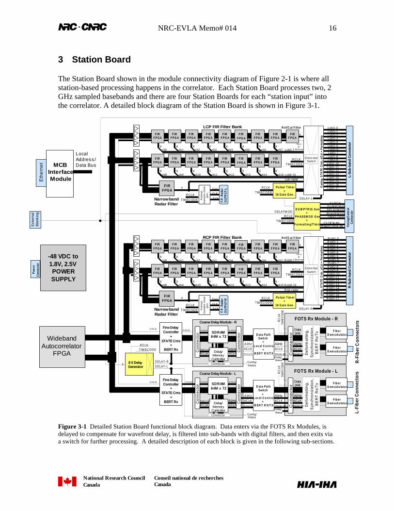
3 Station Board
The Station Board shown in the module connectivity diagram of Figure 2-1 is where allstation-based processing happens in the correlator. Each Station Board processes two, 2GHz sampled basebands and there are four Station Boards for each “station input” intothe correlator. A detailed block diagram of the Station Board is shown in Figure 3-1.
F ib erD em o d u lato r
F ib erD em o d u lato r
De
form
attin
g,
Syn
chro
niz
atio
n,
BE
RT
Rx/
Tx
Co
nn
ecto
r
A1HzAC LK
Data(64)
FOTS Rx Module - R
DVALID
TIM
EC
OD
ER
CLK
D at a Pat hSwit ch
+L ev el C o n t ro l
+B ER T R X /T X
A1HzAC LK
DVALID
AC LK
D V A LI D
A1H z
F ib erD em o d u lato r
F ib erD em o d u lato r
Def
orm
attin
g,
Syn
chro
niz
atio
n,
BE
RT
Rx/
Tx
Co
nn
ecto
r
A1Hz
AC LK
Data(64)
FOTS Rx Module - L
DVALID
TIM
EC
OD
ER
CLK
Fine DelayController
+STATE Cnts
+BERT Rx
Co
nnec
torSDRAM
64M x 72
Co
nnec
tor
Delay/Memory
Controller
A1Hz
D VALIDD VALID
R C LK
Coarse Delay Module - L
ACLKTIMEC OD E
Connector
D at a Pat hSwit ch
+L ev el C o n t ro l
+B ER T R X /T X
A1Hz
AC LK
DVALID
AC LK
D V A LI D
A1H z
Fine DelayController
+STATE Cnts
+BERT Rx
D VALID
D VALID
8sb0
8sb1
8sb2
8sb3
8sb4 sb5 sb6 sb7
8sb8
8sb9
8sb10
8sb11
8sb12 sb13 sb14 sb15
8 8 8
8 8 8
Gat
ing,
STA
TE C
nts,
pC
al +
For
mat
ting
Cross-barSwitch
4
F.P
. Rad
arO
UTP
UT-
L
Fo
rma
t,S
am
ple
clo
ckg
en
.
Data
CLK
T ickR C LK
TIM EC OD E
F IRF P G A
4
D VALID
D VALID
Lsb0-7
Lsb8-15Lsb-radar
R ef /C al F ilt er
L-Su
b-ba
nd C
onne
ctor
LsbO-0LsbO-1LsbO-2LsbO-3LsbO-4LsbO-5LsbO-6LsbO-7LsbO-8LsbO-9
LsbO-10LsbO-11LsbO-12LsbO-13LsbO-14LsbO-15LsbO-16LsbO-17Pu lsar T im er
+16 G at e G en .
8 X DelayGenerator
D U M P T R IG G en .+
PH AS EM O D G en .+
F o rm at t in g /T im in g
1
Tim
ing/
Con
trol
Con
nect
or
C LOC KD U M PTR IGD ELAYM ODPH ASEM ODTIM EC OD E
CLOCK-INTIM EC OD E-IN
R C LKTIM EC OD E
D ELAYM OD
D ELAY-RD ELAY-L
R C LKTIM EC OD E
R C LKT IM EC OD E
R C LKT IM EC OD E
D ELAY-L
-48 VDC to1.8V, 2.5VPOWERSUPPLY
Pow
erC
onne
ctor
LCP FIR Filter Bank
NarrowbandRadar Filter
R-F
iber
Con
nect
ors
L-Fi
ber C
onne
ctor
sConfig/Status
Config/Status
Config/Status
Config/Status
Burs tI/F
Blank ing
WidebandAutocorrelator
FPGA
MCBInterfaceModule
LocalAddress /Data Bus
Eth
erne
t
Co
nne
cto
rSDRAM64M x 72
Co
nne
cto
r
Delay/Memory
Controller
A1Hz
D VALIDD VALID
R C LK
Coarse Delay Module - R
ACLKTIMEC OD E
Connector
F IRF PG A
F IRF PG A
F IRF PG A
F IRF P G A
F IRF PG A
F IRF PG A
F IRF PG A
F IRF P G A
F IRF PG A
F IRF PG A
F IRF PG A
F IRF P G A
F IRF PG A
F IRF PG A
F IRF PG A
F IRF PG A
FIRFPGA
8sb0
8sb1
8sb2
8sb3
8sb4 sb5 sb6 sb7
8sb8
8sb9
8sb10
8sb11
8sb12 sb13 sb14 sb15
8 8 8
8 8 8
Gat
ing,
STA
TE C
nts,
pC
al +
For
mat
ting
Cross-barSwitch
4
F.P
. Rad
arO
UTP
UT-
R
Fo
rma
t,S
am
ple
clo
ckg
en
.
Data
CLK
T ickR C LK
TIM EC OD E
F IRF P G A
4
R sb0-7
R sb8-15R sb-radar
R ef /C al F ilt er
R-S
ub-b
and
Con
nect
or
R sbO-0R sbO-1R sbO-2R sbO-3R sbO-4R sbO-5R sbO-6R sbO-7R sbO-8R sbO-9R sbO-10R sbO-11R sbO-12R sbO-13R sbO-14R sbO-15R sbO-16R sbO-17Pu lsar T im er
+16 G at e G en .
R C LKTIM EC OD E
R C LK
T IM EC OD E
D ELAY-R
RCP FIR Filter Bank
NarrowbandRadar Filter
Burs tI/F
Blank ing
F IRF PG A
F IRF PG A
F IRF PG A
F IRF P G A
F IRF PG A
F IRF PG A
F IRF PG A
F IRF P G A
F IRF PG A
F IRF PG A
F IRF PG A
F IRF P G A
F IRF PG A
F IRF PG A
F IRF PG A
F IRF PG A
FIRFPGA
Ext
erna
lB
lank
ing
Figure 3-1 Detailed Station Board functional block diagram. Data enters via the FOTS Rx Modules, isdelayed to compensate for wavefront delay, is filtered into sub-bands with digital filters, and then exits viaa switch for further processing. A detailed description of each block is given in the following sub-sections.
NRC-EVLA Memo# 014 17
National Research CouncilCanada
Conseil national de recherchesCanada
The Station Board receives data from an antenna via a FOTS receiver module,compensates for wavefront delay, digitally filters the wideband data into sub-bands usingFIR filters, and then formats the data for further downstream processing. The StationBoard also generates all of the additional information such as DUMPTRIG,DELAYMOD, and PHASEMOD that travels with the data for further downstreamprocessing. These additional signals are described in detail in section 4.1.1. Each blockin Figure 3-1 will be described in more detail in the following sub-sections.
3.1 FOTS Rx Module(s)
This mezzanine module will be developed byNRAO as part of the FOTS (Fiber-OpticTransmission System) for the EVLA and willplug into the Station Board motherboard.There could be one module for each (2 GHz)baseband input (as shown in the figure) or therecould be one module for both inputs. Thephysical input to the module is fiber via blind-mate fiber connectors. There may beadditional inputs—for monitor and controlpurposes independent of the Station Board—and these must use blind-mate connectors aswell, otherwise the Station Board can not beinserted as planned.
The module contains the fiber receivers and allof the circuitry for word alignment and error detection/monitoring that are not of concernto the Station Board but are required to ensure link integrity. The module also containstest vector/BERT (Bit Error Rate Test) generation circuitry that allows testing of themodule’s connection to Station Board circuitry. The method used for invoking thistesting capability is TBD.
The signals at the mezzanine card interface connector (which mates with the StationBoard) contain 64 bit streams at 256 Mbits/sec each, a synchronous clock, and asynchronization time tick. The clock and data are synchronous and recovered from thefiber signal. The clock and data are generally not phase synchronous2 with Station Boardclocks and signals. The data are nominally arranged as 16 time-demultiplexed sampleddata streams, with 4 bits/stream for a total sample rate of 4 Gs/sec3. Nominal functionaltiming is illustrated in Figure 3-2. Performance timing parameters, the number of datavalid lines present, and the exact functional and physical interface definition are TBD.Note that other arrangements permitting more, narrower basebands are possible but theclock will always operate at a nominal 128 MHz. If lower bit rate data is present, thendata streams will change states in accordance with their sample rates, but synchronous to
2 Or even phase stable because of receiver phase locking and because this could be data from a VLBIrecorder.3 More correctly it is 4.096 Gs/s, but referred to as 4 Gs/s throughout the document.
F ib erD em o d u lat o r
F ib erD em o d u lat o rD
efor
ma
tting
,S
ynch
roni
zatio
n,
BE
RT
Rx/
Tx
Co
nn
ect
or
A1HzAC LK
Data(64)
FOTS Rx Module - R
DVALID
TIM
EC
OD
ER
CLK
A1HzAC LK
DVALID
F ib erD em o d u lat o r
F ib erD em o d u lat o r
De
form
attin
g,S
ynch
roni
zatio
n,
BE
RT
Rx/
Tx
Co
nn
ecto
r
A1HzAC LK
Data(64)
FOTS Rx Module - L
DVALID
TIM
EC
OD
ER
CLK
A1HzAC LK
DVALID
R-F
iber
Con
nect
ors
L-Fi
ber C
onne
ctor
s
Config/Status
Config/Status
T est v ect o r/D at a Pat h
Switch+
L ev el C o n t ro l+
B ER T R X/T X
T est v ect o r/D at a Pat h
Switch+
L ev el C o n t ro l+
B ER T R X/T X
NRC-EVLA Memo# 014 18
National Research CouncilCanada
Conseil national de recherchesCanada
the 128 MHz clock, and time-aligned to the PPS (1Hz) time tick. TIMECODE may beprovided to the module for future interface considerations.
CLOCK
PPS(1Hz)
D0 t0 t+16 t+32 t+64
D1 t1 t+17 t+33 t+65
D2 t2 t+18 t+34 t+66
D3 t3 t+19 t+35 t+67
D15 t15 t+31 t+63 t+95
Figure 3-2 Nominal functional timing for the FOTs Rx Module to Station Board interface. The data issynchronous to a clock provided to the mezzanine card. Time slot allocations are as indicated in the figureand are bit times at the 4 Gs/s rate. Data at different rates will have different time slot assignments. ThePPS (1 Hz time tick) epoch is for to alignment independent of time slot allocations or actual sampled datarates. This ensures that receiving circuitry and any necessary lower-rate shift clock generation are alwaysresynchronized every PPS.
3.2 Data Path Switch
This block allows BERT testing of the connection tothe FOTS receiver module, the ability to switch datapaths (for data rearrangement or duplication), andthe ability to change bit encoding (in case theencoding does not match the correlator’s internalencoding). As shown in Figure 3-1, there is one ofthese for each of the two baseband inputs.However, increased flexibility will be available ifboth of these are incorporated into one FPGA. This
decision will be based on pin count and cost.
Data PathSwitch
+Level Control
+BERT RX/TX
A1HzACLK
DVALID
ACLK
DVALID
A1Hz
NRC-EVLA Memo# 014 19
National Research CouncilCanada
Conseil national de recherchesCanada
3.3 Coarse Delay Module
The Coarse Delay Module is a mezzanine card4 usedfor wavefront delay compensation. It does this byinserting delay into the entire 16 word wide (64 bit)data path. This compensates for delay to within 16samples at 4 Gs/s. Final delay to within +/-0.5samples at 4 Gs/s is accomplished in the followingFine Delay Controller block. If different basebandbandwidths are used (i.e. on the 64-bit data highway),then each will be delayed the same amount in terms of
absolute time and hence the correct amount in their respective bit times. Differentbaseband input arrangements will require modification of the fine delay logic in thefollowing Fine Delay Controller.
The bulk of the delay memory will be in SDRAM since this is the only affordable way ofintroducing enough delay for the longest earth baselines. Because of the nature of theSDRAM, dual-port SRAM buffers in front and behind the SDRAM will be required.These dual-port buffers can be on the controlling FPGA(s). A 64M deep (576 Mbytes)delay is planned and is enough for 78,000 km of delay (ignoring data transmission delay)at the speed of light, c. If the transmission line from the antenna has a 0.5c speed, thenthe maximum delay (and maximum baseline) is 1/3rd of this or 26,000 km. If thetransmission speed is slower, then the maximum baseline is decreased accordingly.26,000 km is enough for any earth baselines and for moderate space baselines. The goalis to design the module so that additional SDRAM SIMMs can be added if necessary. A72-bit word width is planned to accommodate the 64-bit data highway, some data validlines, the 1 Hz time tick, and perhaps some embedded error check data. Delay controlinformation will come from the Delay Generator block.
The Coarse Delay Module also contains logic that allows the on-board MCBmicroprocessor to write test vectors into it for testing downstream hardware. Since thesetest vectors are in memory, they can be simulated astronomical data complete withDoppler and delay as described in [2], providing a powerful testing facility. Exactoperation requires further definition.
3.4 Fine Delay Controller
This block controls fine delay to within +/-0.5 samples of delay at 4 Gs/s.(N.B. Very fine delay to ±1/32 samples is accomplished with sub-bandphase offsets on the Baseline Board.) It accomplishes this mainly byshifting/swapping data streams and inserting or removing one sample ofdelay. The block also contains wideband data statistics (state counts, and
4 A mezzanine card is planned. However if all of the delay that could ever be required is present—as isnow planned to allow very long baseline connections—then the need for a mezzanine card is not thatevident.
ACLK
DVALID
A1Hz
DVALID
Config/Status
Con
nect
or
SDRAM64M x 72
Con
nect
or
Delay /Memory
Controller
A1Hz
DVALIDDVALID
RCLK
Coarse Delay Module - R
ACLK
TIMECODE
Connector
Fine DelayController
+STATE Cnts
+BERT Rx
NRC-EVLA Memo# 014 20
National Research CouncilCanada
Conseil national de recherchesCanada
power measurement) as well as a BERT receiver for testing connectivity through the datapath up to this point (most importantly through the Coarse Delay Module). Althoughshown as one block for each baseband in Figure 3-1, it may be advantageous to includethis in one device for added flexibility. This will depend on number of I/O, cost, andnumber of outputs required to drive the downstream digital filter banks.
3.5 Wideband Autocorrelator
This function, probably implemented in an FPGA, is to obtain thewideband autocorrelation function for all four possible products (RR,LL, RL, LR) on the wideband data before any digital filtering. Thiswill aid in diagnostic checking and determining where interference ison the wideband signal. It also serves as a double-check to ensure thatdownstream digital filters are operating properly. The number of
spectral channels available, and the sensitivity loss incurred are TBD, but it will operateas a “synthetic” autocorrelator [2] since it is only used for diagnostic purposes and sosome sensitivity loss is unimportant.
3.6 Delay Generator
The Delay Generator block contains 8, 32-bit linearfrequency synthesizers that generate delay for theStation Board. Synthesizers are updated on 10millisecond epochs embedded in the TIMECODEsignal. In the case of the Station Board plugged intothe master slot of the Sub-band Distributor Backplane
(see Figure 2-1), delay for all 8 basebands is generated and merged to form theDELAYMOD (section 4.1.1) signal that travels with the data for very fine delaycorrection on the Baseline Board. Thus, the master Station Board has all 8 synthesizersactive, and the slave Station Boards only have 2 synthesizers active for their own twobasebands. This rather asymmetric arrangement (kludge) is required so that there are noactive electronics on the Sub-band Distributor Backplane. An alternative arrangementmay be possible whereby each Station Board generates its own delays that get fed to themaster Station Board via the backplane for final DELAYMOD generation. The choice ofwhich method to use will be decided during detailed design.
8 X DelayGenerator
RCLKT IM ECODE
DELAY-R
DELAY-LDELAYM OD
WidebandAutocorrelator
FPGA
NRC-EVLA Memo# 014 21
National Research CouncilCanada
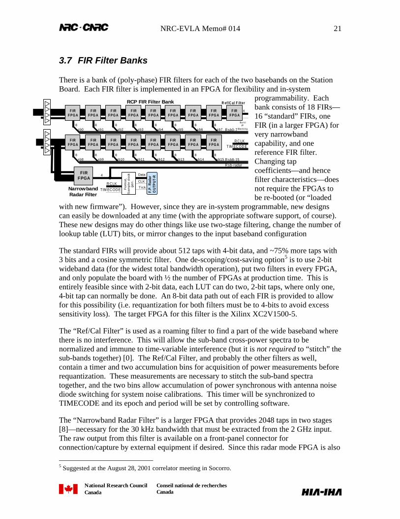
Conseil national de recherchesCanada
3.7 FIR Filter Banks
There is a bank of (poly-phase) FIR filters for each of the two basebands on the StationBoard. Each FIR filter is implemented in an FPGA for flexibility and in-system
programmability. Eachbank consists of 18 FIRs—16 “standard” FIRs, oneFIR (in a larger FPGA) forvery narrowbandcapability, and onereference FIR filter.Changing tapcoefficients—and hencefilter characteristics—doesnot require the FPGAs tobe re-booted (or “loaded
with new firmware”). However, since they are in-system programmable, new designscan easily be downloaded at any time (with the appropriate software support, of course).These new designs may do other things like use two-stage filtering, change the number oflookup table (LUT) bits, or mirror changes to the input baseband configuration
The standard FIRs will provide about 512 taps with 4-bit data, and ~75% more taps with3 bits and a cosine symmetric filter. One de-scoping/cost-saving option5 is to use 2-bitwideband data (for the widest total bandwidth operation), put two filters in every FPGA,and only populate the board with ½ the number of FPGAs at production time. This isentirely feasible since with 2-bit data, each LUT can do two, 2-bit taps, where only one,4-bit tap can normally be done. An 8-bit data path out of each FIR is provided to allowfor this possibility (i.e. requantization for both filters must be to 4-bits to avoid excesssensitivity loss). The target FPGA for this filter is the Xilinx XC2V1500-5.
The “Ref/Cal Filter” is used as a roaming filter to find a part of the wide baseband wherethere is no interference. This will allow the sub-band cross-power spectra to benormalized and immune to time-variable interference (but it is not required to “stitch” thesub-bands together) [0]. The Ref/Cal Filter, and probably the other filters as well,contain a timer and two accumulation bins for acquisition of power measurements beforerequantization. These measurements are necessary to stitch the sub-band spectratogether, and the two bins allow accumulation of power synchronous with antenna noisediode switching for system noise calibrations. This timer will be synchronized toTIMECODE and its epoch and period will be set by controlling software.
The “Narrowband Radar Filter” is a larger FPGA that provides 2048 taps in two stages[8]—necessary for the 30 kHz bandwidth that must be extracted from the 2 GHz input.The raw output from this filter is available on a front-panel connector forconnection/capture by external equipment if desired. Since this radar mode FPGA is also
5 Suggested at the August 28, 2001 correlator meeting in Socorro.
8sb0
8sb1
8sb2
8sb3
8sb4 sb5 sb6 sb7
8sb8
8sb9
8sb10
8sb11
8sb12 sb13 sb14 sb15
8 8 8
8 8 8
4
F.P
. Rad
arO
UTP
UT-
R
Fo
rma
t,S
am
ple
clo
ckg
en
.
Data
CLK
TickR C LK
TIM EC OD E
F IRF P G A
4
R sb0-7
R sb8-15R sb-radar
R ef /C al F ilter
R C LKTIM EC OD E
RCP FIR Filter Bank
NarrowbandRadar Filter
Burs tI/F
Blank ing
F IRF PG A
F IRF P G A
F IRF PG A
F IRF P G A
F IRF P G A
F IRF PG A
F IRF PG A
F IRF P G A
F IRF PG A
F IRF P G A
F IRF PG A
F IRF P G A
F IRF P G A
F IRF PG A
F IRF PG A
F IRF P G A
FIRFPGA
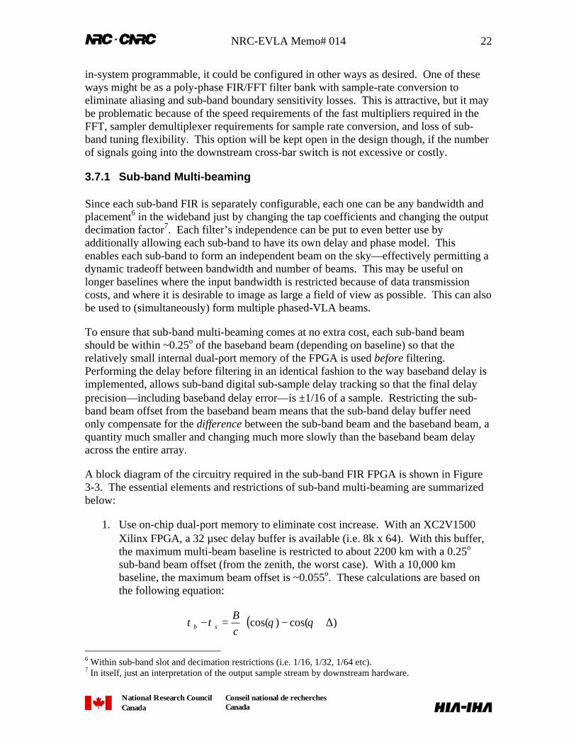
NRC-EVLA Memo# 014 22
National Research CouncilCanada
Conseil national de recherchesCanada
in-system programmable, it could be configured in other ways as desired. One of theseways might be as a poly-phase FIR/FFT filter bank with sample-rate conversion toeliminate aliasing and sub-band boundary sensitivity losses. This is attractive, but it maybe problematic because of the speed requirements of the fast multipliers required in theFFT, sampler demultiplexer requirements for sample rate conversion, and loss of sub-band tuning flexibility. This option will be kept open in the design though, if the numberof signals going into the downstream cross-bar switch is not excessive or costly.
3.7.1 Sub-band Multi-beaming
Since each sub-band FIR is separately configurable, each one can be any bandwidth andplacement6 in the wideband just by changing the tap coefficients and changing the outputdecimation factor7. Each filter’s independence can be put to even better use byadditionally allowing each sub-band to have its own delay and phase model. Thisenables each sub-band to form an independent beam on the sky—effectively permitting adynamic tradeoff between bandwidth and number of beams. This may be useful onlonger baselines where the input bandwidth is restricted because of data transmissioncosts, and where it is desirable to image as large a field of view as possible. This can alsobe used to (simultaneously) form multiple phased-VLA beams.
To ensure that sub-band multi-beaming comes at no extra cost, each sub-band beamshould be within ~0.25o of the baseband beam (depending on baseline) so that therelatively small internal dual-port memory of the FPGA is used before filtering.Performing the delay before filtering in an identical fashion to the way baseband delay isimplemented, allows sub-band digital sub-sample delay tracking so that the final delayprecision—including baseband delay error—is ±1/16 of a sample. Restricting the sub-band beam offset from the baseband beam means that the sub-band delay buffer needonly compensate for the difference between the sub-band beam and the baseband beam, aquantity much smaller and changing much more slowly than the baseband beam delayacross the entire array.
A block diagram of the circuitry required in the sub-band FIR FPGA is shown in Figure3-3. The essential elements and restrictions of sub-band multi-beaming are summarizedbelow:
1. Use on-chip dual-port memory to eliminate cost increase. With an XC2V1500Xilinx FPGA, a 32 µsec delay buffer is available (i.e. 8k x 64). With this buffer,the maximum multi-beam baseline is restricted to about 2200 km with a 0.25o
sub-band beam offset (from the zenith, the worst case). With a 10,000 kmbaseline, the maximum beam offset is ~0.055o. These calculations are based onthe following equation:
( ))cos()cos( ∆+−⋅=− θθττcB
sb
6 Within sub-band slot and decimation restrictions (i.e. 1/16, 1/32, 1/64 etc).7 In itself, just an interpretation of the output sample stream by downstream hardware.
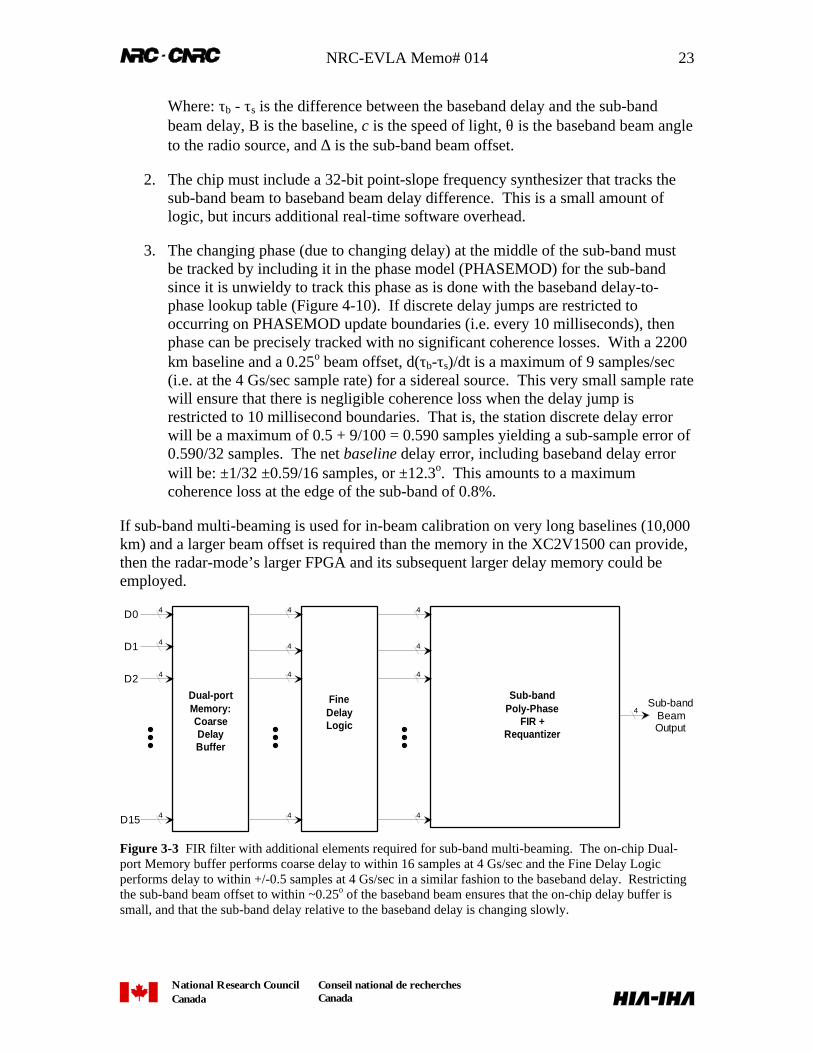
NRC-EVLA Memo# 014 23
National Research CouncilCanada
Conseil national de recherchesCanada
Where: τb - τs is the difference between the baseband delay and the sub-bandbeam delay, B is the baseline, c is the speed of light, θ is the baseband beam angleto the radio source, and ∆ is the sub-band beam offset.
2. The chip must include a 32-bit point-slope frequency synthesizer that tracks thesub-band beam to baseband beam delay difference. This is a small amount oflogic, but incurs additional real-time software overhead.
3. The changing phase (due to changing delay) at the middle of the sub-band mustbe tracked by including it in the phase model (PHASEMOD) for the sub-bandsince it is unwieldy to track this phase as is done with the baseband delay-to-phase lookup table (Figure 4-10). If discrete delay jumps are restricted tooccurring on PHASEMOD update boundaries (i.e. every 10 milliseconds), thenphase can be precisely tracked with no significant coherence losses. With a 2200km baseline and a 0.25o beam offset, d(τb-τs)/dt is a maximum of 9 samples/sec(i.e. at the 4 Gs/sec sample rate) for a sidereal source. This very small sample ratewill ensure that there is negligible coherence loss when the delay jump isrestricted to 10 millisecond boundaries. That is, the station discrete delay errorwill be a maximum of 0.5 + 9/100 = 0.590 samples yielding a sub-sample error of0.590/32 samples. The net baseline delay error, including baseband delay errorwill be: ±1/32 ±0.59/16 samples, or ±12.3o. This amounts to a maximumcoherence loss at the edge of the sub-band of 0.8%.
If sub-band multi-beaming is used for in-beam calibration on very long baselines (10,000km) and a larger beam offset is required than the memory in the XC2V1500 can provide,then the radar-mode’s larger FPGA and its subsequent larger delay memory could beemployed.
Dual-portMemory:CoarseDelayBuffer
4D0
4D1
4D2
4D15
FineDelayLogic
4
4
4
4
Sub-bandPoly-Phase
FIR +Requantizer
4
4
4
4
4Sub-band
BeamOutput
Figure 3-3 FIR filter with additional elements required for sub-band multi-beaming. The on-chip Dual-port Memory buffer performs coarse delay to within 16 samples at 4 Gs/sec and the Fine Delay Logicperforms delay to within +/-0.5 samples at 4 Gs/sec in a similar fashion to the baseband delay. Restrictingthe sub-band beam offset to within ~0.25o of the baseband beam ensures that the on-chip delay buffer issmall, and that the sub-band delay relative to the baseband delay is changing slowly.
NRC-EVLA Memo# 014 24
National Research CouncilCanada
Conseil national de recherchesCanada
An alternative to the above sub-sample delay tracking scheme is to perform digital delaytracking after FIR filtering. In this case, sub-sample delay tracking is performed byupdating the FIR tap coefficients as delay changes. This can be unwieldy and willrequire asynchronous interrupts to the controlling CPU so that tap coefficients areupdated on every 1/16th of a sample change in delay. A tap coefficient buffer is alsorequired in the FIR filter that could consume additional chip resources (depending onhow quickly new coefficients are switched in). Nevertheless, this may be the onlyacceptable solution in the case where the input data is not filtered into many sub-bandsand therefore cannot utilize the previously described method.
3.7.2 7-bit Requantization and Correlation
The requirements for 7-bit requantization and correlation have been studied in [1].However, since the data path for each sub-band from the Station Board to the BaselineBoard is restricted in width to 4 bits, it is necessary to restrict the bandwidth available forcorrelation. There are a few ways of doing this, but probably the best method is torestrict the sub-band bandwidth to ½ its normal maximum when requantizing to 7 bits.The essential elements when 7-bit requantization and correlation are chosen is as follows:
1. The maximum sub-band bandwidth is 64 MHz.
2. The 8-bit output of each FIR filter is used to transport the data to the outputcross-bar switch. Only 7 bits of this is used.
3. The output cross-bar switch multiplexes the 7-bit data @ a 128 MHz clockrate to 4 bits (LSN8) and 3 bits (MSN) at 256 MHz for transmission to thecorrelator. The MSB of the MSN is used for data valid flagging, overcominga previously stated limitation when requantizing to 7 bits.
4. The Recirculation Controller (see section 4.1) demultiplexes the data and setsup the data highways to perform all of the necessary distributed arithmetic.Recirculation is used so that only a factor of 2 reduction in the number ofspectral channels is realized.
Note that the maximum baseband bandwidth that can be correlated with 7 bitrequantization is 1 GHz. Since 7-bit requantization will normally be used when 8-bitinitial quantization is used, the baseband bandwidth is restricted to 1 GHz anyway, and sothis not an additional performance degradation.
The above 7-bit requantization data transport method will also support 7-bit phasing onthe Phasing Board with no additional data path requirements. It will just requirereconfiguration of the Phasing Board FPGAs by either downloading a new logicconfiguration (firmware), or by setting control register bits.
8 Least significant nibble (4 bits).
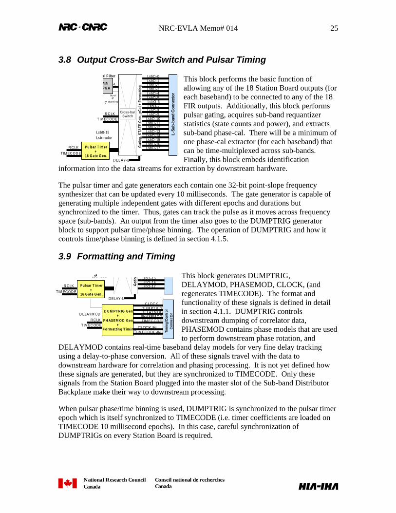
NRC-EVLA Memo# 014 25
National Research CouncilCanada
Conseil national de recherchesCanada
3.8 Output Cross-Bar Switch and Pulsar Timing
This block performs the basic function ofallowing any of the 18 Station Board outputs (foreach baseband) to be connected to any of the 18FIR outputs. Additionally, this block performspulsar gating, acquires sub-band requantizerstatistics (state counts and power), and extractssub-band phase-cal. There will be a minimum ofone phase-cal extractor (for each baseband) thatcan be time-multiplexed across sub-bands.Finally, this block embeds identification
information into the data streams for extraction by downstream hardware.
The pulsar timer and gate generators each contain one 32-bit point-slope frequencysynthesizer that can be updated every 10 milliseconds. The gate generator is capable ofgenerating multiple independent gates with different epochs and durations butsynchronized to the timer. Thus, gates can track the pulse as it moves across frequencyspace (sub-bands). An output from the timer also goes to the DUMPTRIG generatorblock to support pulsar time/phase binning. The operation of DUMPTRIG and how itcontrols time/phase binning is defined in section 4.1.5.
3.9 Formatting and Timing
This block generates DUMPTRIG,DELAYMOD, PHASEMOD, CLOCK, (andregenerates TIMECODE). The format andfunctionality of these signals is defined in detailin section 4.1.1. DUMPTRIG controlsdownstream dumping of correlator data,PHASEMOD contains phase models that are usedto perform downstream phase rotation, and
DELAYMOD contains real-time baseband delay models for very fine delay trackingusing a delay-to-phase conversion. All of these signals travel with the data todownstream hardware for correlation and phasing processing. It is not yet defined howthese signals are generated, but they are synchronized to TIMECODE. Only thesesignals from the Station Board plugged into the master slot of the Sub-band DistributorBackplane make their way to downstream processing.
When pulsar phase/time binning is used, DUMPTRIG is synchronized to the pulsar timerepoch which is itself synchronized to TIMECODE (i.e. timer coefficients are loaded onTIMECODE 10 millisecond epochs). In this case, careful synchronization ofDUMPTRIGs on every Station Board is required.
Gat
ing,
STA
TE C
nts,
pC
al +
For
mat
ting
Cross-barSwitch
4
Lsb0-7
Lsb8-15Lsb-radar
R ef /C al F ilt er
L-Su
b-ba
nd C
onne
ctor
LsbO-0LsbO-1LsbO-2LsbO-3LsbO-4LsbO-5LsbO-6LsbO-7LsbO-8LsbO-9
LsbO-10LsbO-11LsbO-12LsbO-13LsbO-14LsbO-15LsbO-16LsbO-17Pu lsar T im er
+16 G at e G en .
R C LKTIM EC OD E
R C LKT IM EC OD E
D EL AY-L
Burs tI/F
Blank ing
F IRF PG A
LsbO-15LsbO-16LsbO-17Pu lsar T im er
+16 G at e G en .
D U M P T R IG G en .+
PH ASE M O D G en .+
F o rm at tin g /T im in g Tim
ing/
Con
trol
Con
nect
or
C LOC KD U M PT R IGD ELAYM OD
PH ASEM ODTIM EC OD E
CLOCK-INTIM EC OD E-IN
R C LKT IM EC OD E
D ELAYM OD
R C LKTIM EC OD E
D ELAY-L
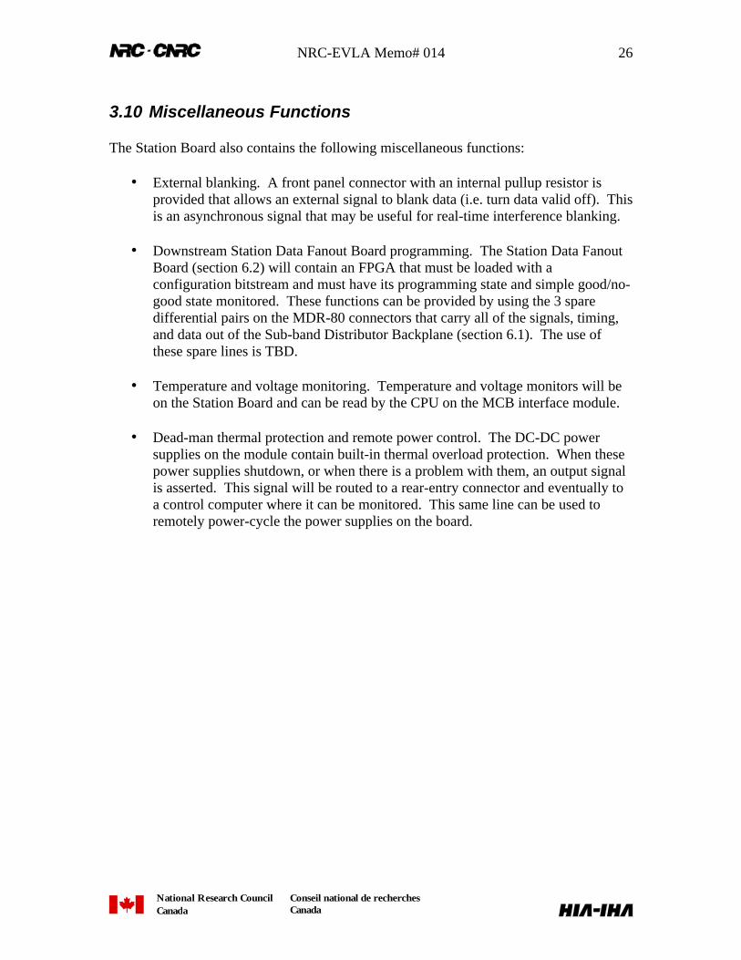
NRC-EVLA Memo# 014 26
National Research CouncilCanada
Conseil national de recherchesCanada
3.10 Miscellaneous Functions
The Station Board also contains the following miscellaneous functions:
• External blanking. A front panel connector with an internal pullup resistor isprovided that allows an external signal to blank data (i.e. turn data valid off). Thisis an asynchronous signal that may be useful for real-time interference blanking.
• Downstream Station Data Fanout Board programming. The Station Data FanoutBoard (section 6.2) will contain an FPGA that must be loaded with aconfiguration bitstream and must have its programming state and simple good/no-good state monitored. These functions can be provided by using the 3 sparedifferential pairs on the MDR-80 connectors that carry all of the signals, timing,and data out of the Sub-band Distributor Backplane (section 6.1). The use ofthese spare lines is TBD.
• Temperature and voltage monitoring. Temperature and voltage monitors will beon the Station Board and can be read by the CPU on the MCB interface module.
• Dead-man thermal protection and remote power control. The DC-DC powersupplies on the module contain built-in thermal overload protection. When thesepower supplies shutdown, or when there is a problem with them, an output signalis asserted. This signal will be routed to a rear-entry connector and eventually toa control computer where it can be monitored. This same line can be used toremotely power-cycle the power supplies on the board.
NRC-EVLA Memo# 014 27
National Research CouncilCanada
Conseil national de recherchesCanada
4 Baseline Board
This section presents a very detailed definition of the Baseline Board design. This levelof detail is provided to ensure that a solid baseline design that meets the highperformance requirements of the correlator is available. A block diagram of the BaselineBoard is shown in Figure 4-1 and for clarity a 2x2 correlator chip ‘slice’ of the board isshown in Figure 4-2. A physical layout of the Baseline Board is shown in a followingsection.
The Baseline Board contains an 8x8 array of 64, 2048 complex-lag correlator chips. Asquare array of chips is used because each array will correlate one “parallelogram” ofbaselines in a large baseline matrix [0]. Each row of correlator chips is fed with datafrom one ‘X’ station using a Recirculation Controller FPGA. Columns are fed with ‘Y’station data in a similar fashion. In this design, each correlator chip has its own dedicatedLTA Controller FPGA and 256 Mbit SDRAM. This arrangement is capable of meetingthe high-speed readout requirements demanded of narrow pulsar phase binning—with1000 phase bins in 2 memory banks—and recirculation using available and affordablehigh-speed DPSRAM memory.
The MCB Interface Module is a small mezzanine board that allows an external computerto configure and monitor all of the devices on the Baseline Board. The MCB modulecontains a CPU that accesses the devices on the board via a dedicated 8-bit (or 16-bit)memory mapped bus. The required address space and bus width is TBD.Communication to the outside world is via 100 Mbit Ethernet. The baseline plan is to usethe MCB mezzanine card that NRAO is developing for other array systems since thedesign should meet the low performance monitor and control requirements and since thismodule will then be standard across all array systems.
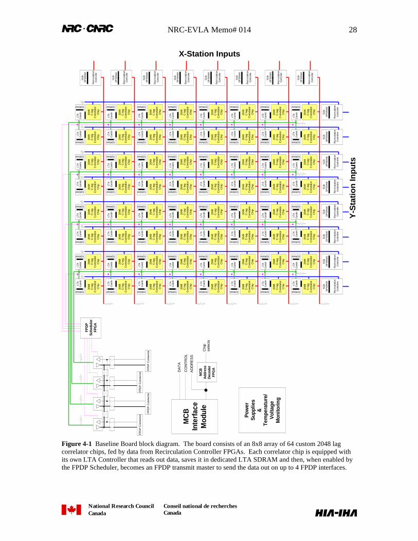
NRC-EVLA Memo# 014 28
National Research CouncilCanada
Conseil national de recherchesCanada
2048
C-la
gC
orre
lato
rC
hipLT
AC
ontrl
r
SDRAM
2048
C-la
gC
orre
lato
rC
hip
LTA
Con
trlr
SDRAM
2048
C-la
gC
orre
lato
rC
hipLT
AC
ontrl
r
SDRAM
2048
C-la
gC
orre
lato
rC
hip
LTA
Con
trlr
SDRAM
2048
C-la
gC
orre
lato
rC
hipLT
AC
ontrl
r
SDRAM
2048
C-la
gC
orre
lato
rC
hip
LTA
Con
trlr
SDRAM
2048
C-la
gC
orre
lato
rC
hipLT
AC
ontrl
r
SDRAM
2048
C-la
gC
orre
lato
rC
hip
LTA
Con
trlr
SDRAM
2048
C-la
gC
orre
lato
rC
hipLT
AC
ontrl
r
SDRAM
2048
C-la
gC
orre
lato
rC
hip
LTA
Con
trlr
SDRAM
2048
C-la
gC
orre
lato
rC
hipLT
AC
ontrl
r
SDRAM
2048
C-la
gC
orre
lato
rC
hip
LTA
Con
trlr
SDRAM
2048
C-la
gC
orre
lato
rC
hipLT
AC
ontrl
r
SDRAM
2048
C-la
gC
orre
lato
rC
hip
LTA
Con
trlr
SDRAM
2048
C-la
gC
orre
lato
rC
hipLT
AC
ontrl
r
SDRAM
2048
C-la
gC
orre
lato
rC
hip
LTA
Con
trlr
SDRAM
2048
C-la
gC
orre
lato
rC
hipLT
AC
ontrl
r
SDRAM
2048
C-la
gC
orre
lato
rC
hip
LTA
Con
trlr
SDRAM
2048
C-la
gC
orre
lato
rC
hipLT
AC
ontrl
r
SDRAM
2048
C-la
gC
orre
lato
rC
hip
LTA
Con
trlr
SDRAM
2048
C-la
gC
orre
lato
rC
hipLT
AC
ontrl
r
SDRAM
2048
C-la
gC
orre
lato
rC
hip
LTA
Con
trlr
SDRAM
2048
C-la
gC
orre
lato
rC
hipLT
AC
ontrl
r
SDRAM
2048
C-la
gC
orre
lato
rC
hip
LTA
Con
trlr
SDRAM
2048
C-la
gC
orre
lato
rC
hipLT
AC
ontrl
r
SDRAM
2048
C-la
gC
orre
lato
rC
hip
LTA
Con
trlr
SDRAM
2048
C-la
gC
orre
lato
rC
hipLT
AC
ontrl
r
SDRAM
2048
C-la
gC
orre
lato
rC
hip
LTA
Con
trlr
SDRAM
2048
C-la
gC
orre
lato
rC
hipLT
AC
ontrl
r
SDRAM
2048
C-la
gC
orre
lato
rC
hip
LTA
Con
trlr
SDRAM
2048
C-la
gC
orre
lato
rC
hipLT
AC
ontrl
r
SDRAM
2048
C-la
gC
orre
lato
rC
hip
LTA
Con
trlr
SDRAM
2048
C-la
gC
orre
lato
rC
hipLT
AC
ontrl
r
SDRAM
2048
C-la
gC
orre
lato
rC
hip
LTA
Con
trlr
SDRAM
2048
C-la
gC
orre
lato
rC
hipLT
AC
ontrl
r
SDRAM
2048
C-la
gC
orre
lato
rC
hip
LTA
Con
trlr
SDRAM
2048
C-la
gC
orre
lato
rC
hipLT
AC
ontrl
r
SDRAM
2048
C-la
gC
orre
lato
rC
hip
LTA
Con
trlr
SDRAM
2048
C-la
gC
orre
lato
rC
hipLT
AC
ontrl
r
SDRAM
2048
C-la
gC
orre
lato
rC
hip
LTA
Con
trlr
SDRAM
2048
C-la
gC
orre
lato
rC
hipLT
AC
ontrl
r
SDRAM
2048
C-la
gC
orre
lato
rC
hip
LTA
Con
trlr
SDRAM
2048
C-la
gC
orre
lato
rC
hipLT
AC
ontrl
r
SDRAM
2048
C-la
gC
orre
lato
rC
hip
LTA
Con
trlr
SDRAM
2048
C-la
gC
orre
lato
rC
hipLT
AC
ontrl
r
SDRAM
2048
C-la
gC
orre
lato
rC
hip
LTA
Con
trlr
SDRAM
2048
C-la
gC
orre
lato
rC
hipLT
AC
ontrl
r
SDRAM
2048
C-la
gC
orre
lato
rC
hip
LTA
Con
trlr
SDRAM
2048
C-la
gC
orre
lato
rC
hipLT
AC
ontrl
r
SDRAM
2048
C-la
gC
orre
lato
rC
hip
LTA
Con
trlr
SDRAM
2048
C-la
gC
orre
lato
rC
hipLT
AC
ontrl
r
SDRAM
2048
C-la
gC
orre
lato
rC
hip
LTA
Con
trlr
SDRAM
2048
C-la
gC
orre
lato
rC
hipLT
AC
ontrl
r
SDRAM
2048
C-la
gC
orre
lato
rC
hip
LTA
Con
trlr
SDRAM
2048
C-la
gC
orre
lato
rC
hipLT
AC
ontrl
r
SDRAM
2048
C-la
gC
orre
lato
rC
hip
LTA
Con
trlr
SDRAM
2048
C-la
gC
orre
lato
rC
hipLT
AC
ontrl
r
SDRAM
2048
C-la
gC
orre
lato
rC
hip
LTA
Con
trlr
SDRAM
2048
C-la
gC
orre
lato
rC
hipLT
AC
ontrl
rSDRAM
2048
C-la
gC
orre
lato
rC
hip
LTA
Con
trlr
SDRAM
2048
C-la
gC
orre
lato
rC
hipLT
AC
ontrl
r
SDRAM
2048
C-la
gC
orre
lato
rC
hip
LTA
Con
trlr
SDRAM
2048
C-la
gC
orre
lato
rC
hipLT
AC
ontrl
r
SDRAM
2048
C-la
gC
orre
lato
rC
hip
LTA
Con
trlr
SDRAM
Rec
ircul
atio
nC
ontro
ller
512k
DP
SR
AM
Rec
ircul
atio
nC
ontro
ller
512k
DP
SR
AM
Rec
ircul
atio
nC
ontro
ller
512k
DP
SR
AM
Rec
ircul
atio
nC
ontro
ller
512k
DP
SR
AM
Rec
ircul
atio
nC
ontro
ller
512k
DP
SR
AM
Rec
ircul
atio
nC
ontro
ller
512k
DP
SR
AM
Rec
ircul
atio
nC
ontro
ller
512k
DP
SR
AM
Rec
ircul
atio
nC
ontro
ller
512k
DP
SR
AM
Rec
ircul
atio
nC
ontro
ller
512k
DP
SR
AM
Rec
ircul
atio
nC
ontro
ller
512k
DP
SR
AM
Rec
ircul
atio
nC
ontro
ller
512k
DP
SR
AM
Rec
ircul
atio
nC
ontro
ller
512k
DP
SR
AM
Rec
ircul
atio
nC
ontro
ller
512k
DP
SR
AM
Rec
ircul
atio
nC
ontro
ller
512k
DP
SR
AM
Rec
ircul
atio
nC
ontro
ller
512k
DP
SR
AM
Rec
ircul
atio
nC
ontro
ller
512k
DP
SR
AM
FP
DP
Con
nect
or
FP
DP
Con
nect
or
FP
DP
Con
nect
or
FP
DP
Con
nect
or
FPD
PSc
hedu
ler
FPG
A
X-Station Inputs
Y-S
tati
on
Inp
uts
MC
BIn
terf
ace
Mod
ule
MC
BA
ddre
ssD
ecod
erFP
GADA
TA
AD
DR
ES
S
CO
NT
RO
L
Chi
pse
lect
s
Pow
erS
uppl
ies
&Te
mpe
ratu
re/
Vol
tage
Mon
itorin
g
Figure 4-1 Baseline Board block diagram. The board consists of an 8x8 array of 64 custom 2048 lagcorrelator chips, fed by data from Recirculation Controller FPGAs. Each correlator chip is equipped withits own LTA Controller that reads out data, saves it in dedicated LTA SDRAM and then, when enabled bythe FPDP Scheduler, becomes an FPDP transmit master to send the data out on up to 4 FPDP interfaces.
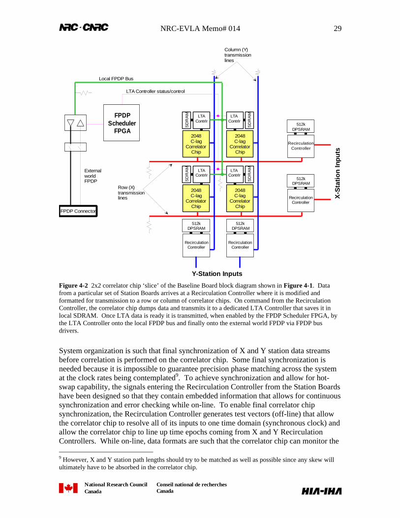
NRC-EVLA Memo# 014 29
National Research CouncilCanada
Conseil national de recherchesCanada
2048C-lag
CorrelatorChip
LTAContrlr
SD
RA
M
2048C-lag
CorrelatorChip
LTAContrlr
SD
RA
M
2048C-lag
CorrelatorChip
LTAContrlr
SD
RA
M2048C-lag
CorrelatorChip
LTAContrlr
SD
RA
M
RecirculationController
512kDPSRAM
RecirculationController
512kDPSRAM
RecirculationController
512kDPSRAM
RecirculationController
512kDPSRAM
FPDP Connector
FPDPScheduler
FPGA
X-S
tati
on
Inp
uts
Y-Station Inputs
Local FPDP Bus
ExternalworldFPDP
Column (Y)transmissionlines
Row (X)transmissionlines
LTA Controller status/control
Figure 4-2 2x2 correlator chip ‘slice’ of the Baseline Board block diagram shown in Figure 4-1. Datafrom a particular set of Station Boards arrives at a Recirculation Controller where it is modified andformatted for transmission to a row or column of correlator chips. On command from the RecirculationController, the correlator chip dumps data and transmits it to a dedicated LTA Controller that saves it inlocal SDRAM. Once LTA data is ready it is transmitted, when enabled by the FPDP Scheduler FPGA, bythe LTA Controller onto the local FPDP bus and finally onto the external world FPDP via FPDP busdrivers.
System organization is such that final synchronization of X and Y station data streamsbefore correlation is performed on the correlator chip. Some final synchronization isneeded because it is impossible to guarantee precision phase matching across the systemat the clock rates being contemplated9. To achieve synchronization and allow for hot-swap capability, the signals entering the Recirculation Controller from the Station Boardshave been designed so that they contain embedded information that allows for continuoussynchronization and error checking while on-line. To enable final correlator chipsynchronization, the Recirculation Controller generates test vectors (off-line) that allowthe correlator chip to resolve all of its inputs to one time domain (synchronous clock) andallow the correlator chip to line up time epochs coming from X and Y RecirculationControllers. While on-line, data formats are such that the correlator chip can monitor the 9 However, X and Y station path lengths should try to be matched as well as possible since any skew willultimately have to be absorbed in the correlator chip.
NRC-EVLA Memo# 014 30
National Research CouncilCanada
Conseil national de recherchesCanada
health of the synchronous connection without having to do a whole bunch of moresophisticated error checking. Thus, when a board is hot-swapped in the system thefollowing steps occur:
1. Power-on the new board and boot-up on-board logic.
2. Tell the Recirculation Controllers to synchronize and align input signals10.
3. Tell the Recirculation Controller to generate test vectors.
4. Tell each correlator chip to receive test vectors and synchronize signals.
5. Once synchronization is achieved, put the Recirculation Controller and correlatorchip in on-line mode.
6. The Recirculation Controllers and correlator chips monitor inputs for transmissionand synchronization errors.
This strategy ensures that only the board that is being replaced is affected—data going toother Baseline Boards does not need to be interrupted to get Recirculation Controllersand correlator chips synchronized.
The Baseline Board also contains temperature and voltage monitoring, dead-man thermalprotection, and remote power-cycle capability as described in section 3.10 on the StationBoard.
The following sections will describe each chip on the Baseline Board and protocolsbetween chips in much more detail. It will be demonstrated that the architecture shownin Figure 4-1 is capable of meeting all of the performance requirements of the EVLA.
4.1 Recirculation Controller
The Recirculation Controller11 is responsible for taking data, timing, and controlinformation from a station (consisting of one sub-band from all 8 basebands) andformatting it for transmission to, and use by, a row or column of correlator chips. Ablack-box diagram of the Recirculation Controller is shown in Figure 4-3. Data andcontrol information12 enters into the right of the box and exits to the correlator chip rowor column on the left. Two banks (devices) of DPSRAM (Dual-Port synchronous StaticRAM) recirculation memory are shown, each one 256k x 18 bits. Two banks are used inping-pong mode to be able to operate up to the 256 Ms/s rate (i.e. each RAM is capableof ~133 MHz). The total memory depth—which sets the data burst length and thecorrelator chip readout time—is 512k. At the maximum synthesized lag length of 512k
10 It is thought that it is better to have the Recirculation Controller synchronize and align signals oncommand rather than have it do it continuously and autonomously.11 Calling it a Recirculation Controller is a bit of a misnomer. It does perform this function, but it performsmany others as well.12 Each signal uses two differential transmission lines.
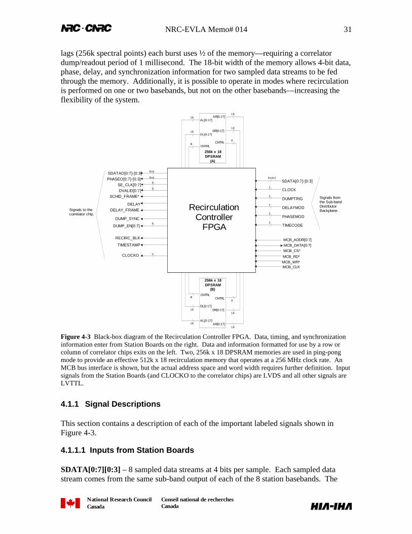
NRC-EVLA Memo# 014 31
National Research CouncilCanada
Conseil national de recherchesCanada
lags (256k spectral points) each burst uses ½ of the memory—requiring a correlatordump/readout period of 1 millisecond. The 18-bit width of the memory allows 4-bit data,phase, delay, and synchronization information for two sampled data streams to be fedthrough the memory. Additionally, it is possible to operate in modes where recirculationis performed on one or two basebands, but not on the other basebands—increasing theflexibility of the system.
256k x 18DPSRAM
(A)
AR[0:17]
DR[0:17]
CNTRL
18
18
8
AL[0:17]
DL[0:17]
CNTRL
18
18
8
256k x 18DPSRAM
(B)
AR[0:17]
DR[0:17]
CNTRL
18
18
8
AL[0:17]
DL[0:17]
CNTRL
18
18
8
8x4x2SDATA[0:7]-[0:3]
2CLOCK
DUMPTRIG
DELAYMOD
PHASEMOD
TIMECODE
2
2
2
2
8x4SDATAO[0:7]-[0:3]8x4PHASEO[0:7]-[0:3]
8SE_CLK[0:7]
8DVALID[0:7]
CLOCKO
8DUMP_EN[0:7]
DELAYDELAY_FRAME
RECIRC_BLK
TIMESTAMP
RecirculationController
FPGA
Signals fromthe Sub-bandDistributorBackplane.
SCHID_FRAME*
2
DUMP_SYNC
Signals to thecorrelator chip.
MCB_ADDR[0:7]MCB_DATA[0:7]MCB_CS*
MCB_RD*
MCB_CLKMCB_WR*
Figure 4-3 Black-box diagram of the Recirculation Controller FPGA. Data, timing, and synchronizationinformation enter from Station Boards on the right. Data and information formatted for use by a row orcolumn of correlator chips exits on the left. Two, 256k x 18 DPSRAM memories are used in ping-pongmode to provide an effective 512k x 18 recirculation memory that operates at a 256 MHz clock rate. AnMCB bus interface is shown, but the actual address space and word width requires further definition. Inputsignals from the Station Boards (and CLOCKO to the correlator chips) are LVDS and all other signals areLVTTL.
4.1.1 Signal Descriptions
This section contains a description of each of the important labeled signals shown inFigure 4-3.
4.1.1.1 Inputs from Station Boards
SDATA[0:7][0:3] – 8 sampled data streams at 4 bits per sample. Each sampled datastream comes from the same sub-band output of each of the 8 station basebands. The
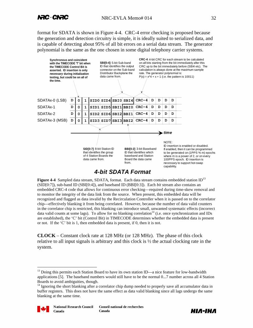
NRC-EVLA Memo# 014 32
National Research CouncilCanada
Conseil national de recherchesCanada
format for SDATA is shown in Figure 4-4. CRC-4 error checking is proposed becausethe generation and detection circuitry is simple, it is ideally suited to serialized data, andis capable of detecting about 95% of all bit errors on a serial data stream. The generatorpolynomial is the same as the one chosen in some digital telephony carrier systems.
D SID0 SID4 SBI0 SBI4 D D D D
D SID1 SID5 SBI1 BBI0 D D D D
D SID2 SID6 SBI2 BBI1 D D D D
D SID3 SID7 SBI3 BBI2 D D D D
0
0
0
0
CRC-4
CRC-4
CRC-4
CRC-4
SDATAx-0 (LSB)
SDATAx-1
SDATAx-2
SDATAx-3 (MSB)
Synchronous and coincident with the TIMECODE 'T' bit when the TIMECODE Control Bit is asserted. ID insertion is only necessary during initialization testing, but could be on all of the time.
SID[0:7]: 8-bit Station IDthat identifies the groupof 4 Station Boards thedata came from.
SBI[0:4]: 5-bit Sub-bandID that identifies the outputconnector on the Sub-bandDistributor Backplane thedata came from.
BBI[0:2]: 3-bit BasebandID that identifies whichbaseband and StationBoard the data camefrom.
4-bit SDATA Format
time
CRC-4: 4-bit CRC for each stream to be calculatedon all bits starting from the bit immediately after thisCRC up to the bit immediately before (SBI4 etc). Thecalculation is always done at the maximum samplerate. The generator polynomial is:P(x) = x^4 + x + 1 (i.e. the pattern is 10011)
NOTE:ID insertion is enabled or disabled.If enabled, then it can be programmedto be generated on (1PPS % m) epochswhere m is a power of 2, or on every100PPS epoch. ID insertion isnecessary to support hot-swapcapability.
1
1
1
1
Figure 4-4 Sampled data stream, SDATA, format. Each data stream contains embedded station ID13
(SID[0:7]), sub-band ID (SBI[0:4]), and baseband ID (BBI[0:3]). Each bit stream also contains anembedded CRC-4 code that allows for continuous error checking—required during time-skew removal andto monitor the integrity of the data link from the source. When present, this embedded data will berecognized and flagged as data invalid by the Recirculation Controller when it is passed on to the correlatorchip—effectively blanking it from being correlated. However, because the number of data valid countersin the correlator chip is restricted, this blanking can introduce small, unwanted systematic effects (incorrectdata valid counts at some lags). To allow for no blanking correlation14 (i.e. once synchronization and IDsare established), the ‘C’ bit (Control Bit) in TIMECODE determines whether the embedded data is presentor not. If the ‘C’ bit is 1, then embedded data is present, if 0, then it is not.
CLOCK – Constant clock rate at 128 MHz (or 128 MHz). The phase of this clockrelative to all input signals is arbitrary and this clock is ½ the actual clocking rate in thesystem.
13 Doing this permits each Station Board to have its own station ID—a nice feature for low-bandwidthapplications [5]. The baseband numbers would still have to be the normal 0...7 number across all 4 StationBoards to avoid ambiguities, though.14 Ignoring the short blanking after a correlator chip dump needed to properly save all accumulator data inbuffer registers. This does not have the same effect as data valid blanking since all lags undergo the sameblanking at the same time.
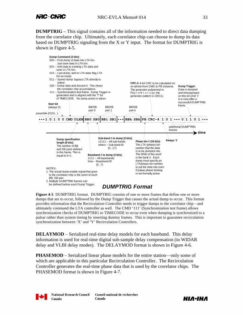
NRC-EVLA Memo# 014 33
National Research CouncilCanada
Conseil national de recherchesCanada
DUMPTRIG – This signal contains all of the information needed to direct data dumpingfrom the correlator chip. Ultimately, each correlator chip can choose to dump its databased on DUMPTRIG signaling from the X or Y input. The format for DUMPTRIG isshown in Figure 4-5.
0 1 0 0 CRC-4DLEN BB0 SB0 BB1 SB1 BBk SBk PBCMD 1 10 10 1 0 11
time
preamble (0101...)
Start bit(always 0)
Dump specificationlength (8 bits):The number of BBand SB pairs definedin this frame. This isequal to k+1. Baseband # to dump (4 bits):
1111 -- All basebands0xxx -- Baseband ID (0...7)
Sub-band # to dump (5 bits):11111 -- All sub-bandsothers -- Sub-band ID (0...17)
BB/SBpair 0
BB/SBpair 1
BB/SBpair k
Phase bin # (16 bits):The LTA (phase) binnumber that the datais to be dumped into.The MSB of this wordis the bank #. Eachdump must specify anLTA/phase bin numberto put the data into evenif pulsar phase binningis not formally active.
Dump Command (3 bits):000 -- First dump of data into LTA bin. Just save data in LTA bin.001 -- Add data to existing LTA data and save in LTA bin.010 -- Last dump: add to LTA data; flag LTA bin as ready.011 -- Speed dump: bypass LTA directly to output.100 -- Dump data and discard it. This clears the correlator chip accumulators.111 -- Synchronization test frame. Dump Trigger is generated and is aligned with the 'T' bit of TIMECODE. No dump action is taken.
CRC-4: 4-bit CRC to be calculated onon all bits from CMD to PB inclusive.The generator polynomial is:P(x) = x^4 + x + 1 (or, thegenerator pattern is 10011)
Dump Trigger:Data is dumpedand timestampedon this bit (2nd '1'in a row) after asuccessful DUMPTRIGframe.
Always '1'
DUMPTRIG Format
NOTES:1. The actual dump enable signal that goes to the correlator chip is the union of each BB, SB pair.2. Multiple DUMPTRIG frames can be defined before each Dump Trigger.
additional DUMPTRIGframes
Figure 4-5 DUMPTRIG format. DUMPTRIG consists of one or more frames that define one or moredumps that are to occur, followed by the Dump Trigger that causes the actual dump to occur. This formatprovides information that the Recirculation Controller needs to trigger dumps to the correlator chip—andultimately command the LTA controller as well. The CMD ‘111’ (Synchronization test frame) allowssynchronization checks of DUMPTRIG to TIMECODE to occur even when dumping is synchronized to apulsar rather than system timing by inserting dummy frames. This is important to guarantee recirculationsynchronization between ‘X’ and ‘Y’ Recirculation Controllers.
DELAYMOD – Serialized real-time delay models for each baseband. This delayinformation is used for real-time digital sub-sample delay compensation (in WIDARdelay and VLBI delay modes). The DELAYMOD format is shown in Figure 4-6.
PHASEMOD – Serialized linear phase models for the entire station—only some ofwhich are applicable to this particular Recirculation Controller. The RecirculationController generates the real-time phase data that is used by the correlator chips. ThePHASEMOD format is shown in Figure 4-7.
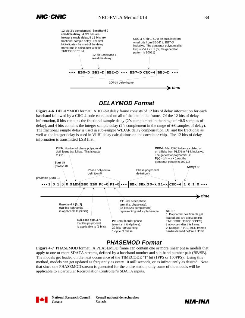
NRC-EVLA Memo# 014 34
National Research CouncilCanada
Conseil national de recherchesCanada
BB0-D BB1-D BB2-D BB7-D CRC-4 BB0-D
time
DELAYMOD Format
100-bit delay frame
12-bit (2's complement) BaseBand 0real-time delay. 4 MS bits areinteger sample delay, 8 LS bits arefractional sample delay. The firstbit indicates the start of the delayframe and is coincident with theTIMECODE 'T' bit.
CRC-4: 4-bit CRC to be calculated onon all bits from BB0-D to BB7-Dinclusive. The generator polynomial is:P(x) = x^4 + x + 1 (or, the generatorpattern is 10011)
12-bit BaseBand 1real-time delay...
Figure 4-6 DELAYMOD format. A 100-bit delay frame consists of 12 bits of delay information for eachbaseband followed by a CRC-4 code calculated on all of the bits in the frame. Of the 12 bits of delayinformation, 8 bits contains the fractional sample delay (2’s complement in the range of ±0.5 samples ofdelay), and 4 bits contains the integer sample delay (2’s complement in the range of ±8 samples of delay).The fractional sample delay is used in sub-sample WIDAR delay compensation [3], and the fractional aswell as the integer delay is used in VLBI delay calculations on the correlator chip. The 12 bits of delayinformation is transmitted LSB first.
0 1 0 01 PLEN BB0 SB0 P0-0 P1-0 BBk SBk P0-k P1-k CRC-4 0 11 0
Start bit(always 0)
PLEN: Number of phase polynomialdefinitions that follow. This is equalto k+1.
Phase polynomialdefinition 0
Phase polynomialdefinition k
CRC-4: 4-bit CRC to be calculated onon all bits from PLEN to P1-k inclusive.The generator polynomial is:P(x) = x^4 + x + 1 (or, thegenerator pattern is 10011)
Always '1'
preamble (0101...)
time
Baseband # (0...7)that this polynomialis applicable to (3 bits)
Sub-band # (0...17)that this polynomialis applicable to (5 bits).
P0: Zero-th order phaseterm (i.e. initial phase).32-bits representing1 cycle of phase.
P1: First order phaseterm (i.e. phase rate).32-bits (2's complement)representing +/-1 cycle/sample. NOTE:
1. Polynomial coefficients getloaded and are active on theTIMECODE 'T' bit (100PPS)that occurs after this frame.2. Multiple PHASEMOD framescan be defined before a 'T' bit.
PHASEMOD FormatFigure 4-7 PHASEMOD format. A PHASEMOD frame can contain one or more linear phase models thatapply to one or more SDATA streams, defined by a baseband number and sub-band number pair (BB/SB).The models get loaded on the next occurrence of the TIMECODE ‘T’ bit (1PPS or 100PPS). Using thismethod, models can get updated as frequently as every 10 milliseconds, or as infrequently as desired. Notethat since one PHASEMOD stream is generated for the entire station, only some of the models will beapplicable to a particular Recirculation Controller’s SDATA inputs.
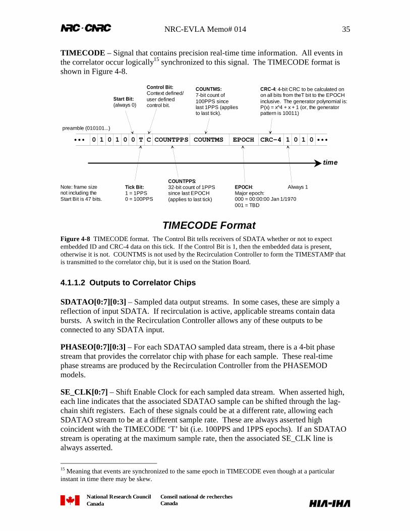
NRC-EVLA Memo# 014 35
National Research CouncilCanada
Conseil national de recherchesCanada
TIMECODE – Signal that contains precision real-time time information. All events inthe correlator occur logically15 synchronized to this signal. The TIMECODE format isshown in Figure 4-8.
1 0 1 0 00 T COUNTMSCOUNTPPS EPOCH CRC-4 1 1 00C
Start Bit:(always 0)
time
Tick Bit:1 = 1PPS0 = 100PPS
COUNTMS:7-bit count of100PPS sincelast 1PPS (appliesto last tick).
COUNTPPS:32-bit count of 1PPSsince last EPOCH(applies to last tick)
EPOCH:Major epoch:000 = 00:00:00 Jan 1/1970001 = TBD
CRC-4: 4-bit CRC to be calculated onon all bits from theT bit to the EPOCHinclusive. The generator polynomial is:P(x) = x^4 + x + 1 (or, the generatorpattern is 10011)
preamble (010101...)
Always 1
TIMECODE Format
Note: frame sizenot including theStart Bit is 47 bits.
Control Bit:Context defined/user definedcontrol bit.
Figure 4-8 TIMECODE format. The Control Bit tells receivers of SDATA whether or not to expectembedded ID and CRC-4 data on this tick. If the Control Bit is 1, then the embedded data is present,otherwise it is not. COUNTMS is not used by the Recirculation Controller to form the TIMESTAMP thatis transmitted to the correlator chip, but it is used on the Station Board.
4.1.1.2 Outputs to Correlator Chips
SDATAO[0:7][0:3] – Sampled data output streams. In some cases, these are simply areflection of input SDATA. If recirculation is active, applicable streams contain databursts. A switch in the Recirculation Controller allows any of these outputs to beconnected to any SDATA input.
PHASEO[0:7][0:3] – For each SDATAO sampled data stream, there is a 4-bit phasestream that provides the correlator chip with phase for each sample. These real-timephase streams are produced by the Recirculation Controller from the PHASEMODmodels.
SE_CLK[0:7] – Shift Enable Clock for each sampled data stream. When asserted high,each line indicates that the associated SDATAO sample can be shifted through the lag-chain shift registers. Each of these signals could be at a different rate, allowing eachSDATAO stream to be at a different sample rate. These are always asserted highcoincident with the TIMECODE ‘T’ bit (i.e. 100PPS and 1PPS epochs). If an SDATAOstream is operating at the maximum sample rate, then the associated SE_CLK line isalways asserted.
15 Meaning that events are synchronized to the same epoch in TIMECODE even though at a particularinstant in time there may be skew.
NRC-EVLA Memo# 014 36
National Research CouncilCanada
Conseil national de recherchesCanada
DVALID[0:7] – There is one of these DVALID lines for each SDATAO sample stream.These are asserted active high to indicate that the associated SDATAO sample is valid.Note that the SDATA input to the Recirculation Controller normally uses one state (-8:1000b) to indicate that data is invalid. If enabled, the Recirculation Controller interceptsthis state and negates the associated DVALID line. If not enabled, the –8 state passesthrough without affecting the DVALID line—needed to support 7-bit correlation [1].
SCHID_FRAME* - This signal is asserted for one CLOCKO cycle to indicate thebeginning of information embedded in the SDATAO data streams. This signal is onlyasserted when the TIMECODE Control Bit is asserted.
DELAY – This signal contains real-time delay information for each SDATAO stream.This signal is normally used by the correlator chip in VLBI modes where the normal sub-sample delay tracking mechanism is not used because the original real-time sample rateof the sampled data stream is only twice the bandwidth. X and Y DELAY information isused on the correlator chip to generate the baseline-based fine/vernier delay and phasemodifier [2].
DELAY_FRAME – A framing/synchronization signal for DELAY. Each DELAYframe consists of 100 bits.
DUMP_SYNC – This signal is asserted when at least one of the DUMP_EN lines isasserted and indicates the beginning of information on the RECIRC_BLK andTIMESTAMP lines. Correlator chip dumping can occur logically synchronized toastronomical events and so this does not, in general, occur when SCHID_FRAME*occurs.
DUMP_EN[0:7] – Each of these signals indicates that a set of correlator chip lagsconnected to the associated SDATAO data stream should be dumped. Whether dumpingactually occurs in the correlator chip depends on whether the correlator chip has beenprogrammed to dump on an X or Y station command. These signals also containadditional information such as the dump command, the LTA/phase bin the dump is to goto, the harmonic suppression phase that needs to be removed prior to accumulation in theLTA, and the correlation “holdoff” indication.
RECIRC_BLK – This line contains the recirculation block counter for the assertedDUMP_EN lines. The correlator chip simply captures this counter and includes it in theassociated output data frame for downstream processing. Details of how recirculation isimplemented are contained in following sections.
TIMESTAMP – This line contains 64-bit timestamp information for the dump. This is aderived copy of TIMECODE when the most recent DUMP_SYNC occurred.TIMESTAMP word 0 (refer to Figure 4-9) is a copy of the TIMECODE COUNTPPS(i.e. number of seconds since the epoch). Word 1, bits 0...28, is a count of the number ofclocks (at the maximum rate of 256 MHz) since the last 1PPS. Word 1, bits 29...31, isthe epoch from TIMECODE. This format ensures that the dump is accurately andprecisely timestamped when dumping is synchronized to astronomical events (pulsars).
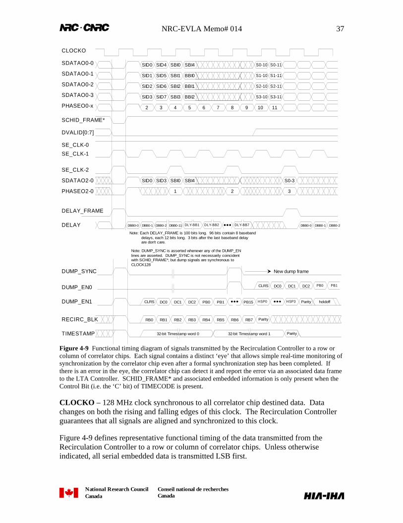
NRC-EVLA Memo# 014 37
National Research CouncilCanada
Conseil national de recherchesCanada
CLOCKO
SDATAO0-0
SDATAO0-1
SDATAO0-2
SDATAO0-3
SID0
SID1
SID2
SID3
SID4
SID5
SID6
SID7
SBI0
SBI1
SBI2
SBI3
SBI4
BBI0
BBI1
BBI2
SCHID_FRAME*
DVALID[0:7]
SE_CLK-0
SE_CLK-1
SE_CLK-2
SDATAO2-0 SID0 SID3 SBI0 SBI4 S0-3
PHASEO0-x 6 7 8
PHASEO2-0 3
DELAY_FRAME
DELAY DBB0-0 DLY-BB1 DLY-BB2 DLY-BB7DBB0-1 DBB0-2 DBB0-11 DBB0-0 DBB0-1 DBB0-2
DUMP_EN0
DUMP_EN1
Note: DUMP_SYNC is asserted whenever any of the DUMP_ENlines are asserted. DUMP_SYNC is not necessarily coincidentwith SCHID_FRAME*; but dump signals are synchronous to CLOCK128
RB0 RB1 RB2 RB3 RB4 RB5 RB6 RB7 ParityRECIRC_BLK
DUMP_SYNC
DC0 DC1CLRS
TIMESTAMP 32-bit Timestamp word 0 Parity
HSP0 HSP3
DC0 DC1CLRS PB0 PB1
ParityDC2
DC2
S0-10
S1-10
S2-10
S3-10
9 105432
21
Note: Each DELAY_FRAME is 100 bits long. 96 bits contain 8 baseband delays, each 12 bits long. 3 bits after the last baseband delay are don't care.
32-bit Timestamp word 1
PB0 PB1 PB15
New dump frame
S0-11
S1-11
S2-11
S3-11
11
holdoff
Figure 4-9 Functional timing diagram of signals transmitted by the Recirculation Controller to a row orcolumn of correlator chips. Each signal contains a distinct ‘eye’ that allows simple real-time monitoring ofsynchronization by the correlator chip even after a formal synchronization step has been completed. Ifthere is an error in the eye, the correlator chip can detect it and report the error via an associated data frameto the LTA Controller. SCHID_FRAME* and associated embedded information is only present when theControl Bit (i.e. the ‘C’ bit) of TIMECODE is present.
CLOCKO – 128 MHz clock synchronous to all correlator chip destined data. Datachanges on both the rising and falling edges of this clock. The Recirculation Controllerguarantees that all signals are aligned and synchronized to this clock.
Figure 4-9 defines representative functional timing of the data transmitted from theRecirculation Controller to a row or column of correlator chips. Unless otherwiseindicated, all serial embedded data is transmitted LSB first.
NRC-EVLA Memo# 014 38
National Research CouncilCanada
Conseil national de recherchesCanada
The DUMP_ENx control bits are defined as follows:
• CLRS – If set (1), then any lag shift registers that use data from the associatedsampled data stream are cleared. This must be done after every recirculation burstto avoid incorrect correlation of non-contiguous time chunks of data (although,strictly speaking, the correlation holdoff function eliminates the need for this bit).
• DC[0:3] – This is identical to the dump command ‘CMD’ defined in theDUMPTRIG format of Figure 4-5 except that the synchronization test frame(CMD=’111’) is never generated. This command is passed on by the correlatorchip to the downstream LTA Controller.
• PB[0:15] – This is the 16-bit phase bin number encoded in the DUMPTRIGcommand. Each DUMP_ENx line could have its own unique phase binnumber—possibly required when mixing recirculation and non-recirculationmodes and different bandwidth sub-bands. This is passed on by the correlatorchip to the LTA Controller. Although the LTA controller only provides for twobanks of 1000 phase bins, if the dump command is a speed dump (011), then allof these phase bins could be utilized by a downstream computer.
• HSP[0:3] – Harmonic suppression phase. This is a phase offset for this dumpthat the LTA Controller (or downstream computing engine) must remove beforeintegrating with other data. This is to help attenuate narrowband signal harmonicsgenerated by the quantizer [4]. This phase is simply passed on by the correlatorchip to the LTA Controller.
In addition, the DUMP_ENx signal functions as a “correlation holdoff” by staying highuntil correlation should start. This function is necessary to eliminate edge effects whenrecirculation is active by providing a mechanism to allow the lag shift register to fill upwith data before correlation begins.
4.1.2 Simplified Block DiagramA simplified block diagram of the Recirculation Controller FPGA is shown in Figure4-10.
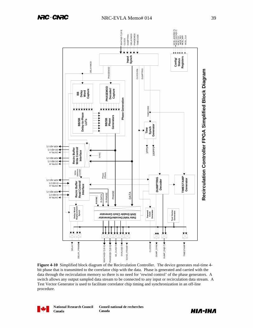
NRC-EVLA Memo# 014 39
National Research CouncilCanada
Conseil national de recherchesCanada
Inpu
tS
ynch
SD
AT
A[0
:7]-
[0:3
]
CLO
CK
DU
MP
TR
IG
DE
LAY
MO
D
PH
AS
EM
OD
TIM
EC
OD
E
DU
MP
TR
IGD
eco
der
TIM
ES
TAM
PG
ener
ator
BB
Del
ayW
ord
Cap
ture
BB
/SB
Del
ay-t
o-Ph
ase
LUTs
BB
/SB
Pha
seG
ener
ator
s
Pha
se G
ener
atio
n
PHA
SE
MO
DD
ecod
er/
Cap
ture
Rec
irc B
uffe
rW
rite
Con
trol
/In
terf
ace
Rec
irc B
uffe
rR
ead
Con
trol
/In
terf
ace
Writ
eA
ddre
ssC
ount
er
Del
ay W
ord
Rep
lace
men
t/S
ynch
DU
MP
_SY
NC
DU
MP
_EN
[0:7
]
Tim
eS
ynch
Gen
erat
or
1PP
S
100P
PS
TIM
ES
TAM
P
Data Valid Decoder/GeneratorShift Enable Clock Generator
DA
TA
PH
AS
E
R-P
HA
SE
R-D
AT
A
DE
LAY
DE
LAY
_FR
AM
E
SD
AT
AO
[0:7
]-[0
:3]
PH
AS
EO
[0:7
]-[0:
3]
SE
_CLK
[0:7
]
DV
ALI
D[0
:7]
SC
HID
_FR
AM
E*
Tran
smit
Clo
ckG
ener
ator
CLO
CK
O
PH
AS
EM
OD
DE
LAY
MO
D
CLO
CK
256
DU
MP
TR
IG
TIM
EC
OD
E
ADR-A[0:17]
DO-A[0:17]CNTRL-A
ADR-B[0:17]
DO-B[0:17]CNTRL-B
ADR-A[0:17]
DI-A[0:17]CNTRL-A
ADR-B[0:17]
DI-B[0:17]CNTRL-B
Rec
ircu
lati
on
Co
ntr
olle
r F
PG
A S
imp
lifie
d B
lock
Dia
gra
m
Con
fig/
Sta
tus
Reg
iste
rs
MC
B_
AD
DR
[0:7
]M
CB
_DA
TA
[0:7
]M
CB
_C
S*
MC
B_R
D*
MC
B_C
LK
MC
B_W
R*
R-S
YN
C
Pha
seO
ffset
s
SY
NC
Tes
t V
ecto
rG
ener
ato
r
Figure 4-10 Simplified block diagram of the Recirculation Controller. The device generates real-time 4-bit phase that is transmitted to the correlator chip with the data. Phase is generated and carried with thedata through the recirculation memory so there is no need for ‘rewind control’ of the phase generators. Aswitch allows any output sampled data stream to be connected to any input or recirculation data stream. ATest Vector Generator is used to facilitate correlator chip timing and synchronization in an off-lineprocedure.
NRC-EVLA Memo# 014 40
National Research CouncilCanada
Conseil national de recherchesCanada
The Recirculation Controller’s main functions are phase generation, recirculation control,reformatting data for the correlator chips, and facilitating final signal synchronizationbefore correlation using the Test Vector Generator. The Test Vector Generator can beswitched on and replaces all data going to the row or column of correlator chips. Thisallows each correlator chip to synchronize its X and Y input data to the same timedomain (clock), line up timing epochs (100PPS and 1PPS), and test the integrity of theinput signals. Once alignment and signal integrity is checked, the RecirculationController generates normal data as outlined in Figure 4-9. The actual test vectorsequence requires further definition but it will probably be a LFSR (linear feedback shiftregister) pseudo-random code synchronized to an embedded 100PPS signal transmittedon SCHID_FRAME*16.
4.1.3 Input Timing and SynchronizationThe data, timing, and control signals arriving at the Recirculation Controller will havetraveled over about 13 m of cable, several inches of backplane, and through severalconnectors on its way from the Station Boards. There is one repeater (on the Station DataFanout Board) in this path that resynchronizes and re-times the data, but a conservativeestimate is that the data and clock will arrive—at the Recirculation Controller and theStation Data Fanout Board—skewed in time. With resynchronization logic and the codesand error checking embedded in the signals, it is possible to remove this skew and presentthe rest of the chip’s internal logic with deskewed data synchronized to the internal 256MHz clock. A schematic of the logic required for each input is shown in Figure 4-11(ref: Xilinx application note XAPP225 v1.0, Sept. 2000).
The circuitry in Figure 4-11 requires a 256 MHz clock and a 256 MHz clock with a 90o
phase-shift. Unfortunately, the Virtex-E17 DLL (Delay Lock Loop) cannot generate a256 MHz 90o phase-shift clock from an input clock of 128 MHz because of DLLfrequency limitations. A workaround to this problem is shown in Figure 4-12. Anexternal delay line of 1 nsec creates a 45o phase-shift at 128 MHz that is then fed into anadditional clock input to the device. Two separate DLLs then double the clock—yieldingthe desired clock phases and a 128 MHz clock to be used for the ping-pong recirculationDPSRAM.
16 SCHID_FRAME* cannot simply be a tick asserted every 100PPS because the correlator chip will notknow for sure if this tick is being properly timed and received on its own.17 The newly available Virtex-II devices can handle 256 MHz clock generation without an external delay sothis may be a mute point.
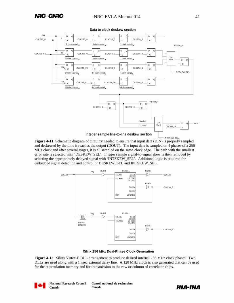
NRC-EVLA Memo# 014 41
National Research CouncilCanada
Conseil national de recherchesCanada
D
C
Q
D
C
Q
D
C
Q
D
C
Q
D
C
Q
D
C
Q
D
C
Q
D
C
Q
D
C
Q
D
C
Q
D
C
Q
D
C
Q
CLK256_0
CLK256_90
CLK256_0
CLK256_0
CLK256_90
CLK256_0
CLK256_0
CLK256_0
CLK256_0
CLK256_90
1:4MUX D
C
Q
CLK256_0
DESKEW_SEL
D
C
Q
1:4MU X
D
C
Q
CLK256_0D
C
QCLK256_0
DIN
CLK256_0DOUT
INTSKEW_SEL
Data to clock deskew section
Integer sample line-to-line deskew section
0
90
180
270
1 clock period
3/4 clock period
3/4 clock period
1 clock period
1 clock period
3/4 clock period
3/4 clock period
3/4 clock period
D
C
Q
D
C
Q
D
C
Q
D
C
Q
CLK256_0
CLK256_0
CLK256_0
CLK256_0
3/4 clock period
1 clock period
1 clock period
1 clock period
"0 delay"
"-1 delay"
"+1 delay"
Figure 4-11 Schematic diagram of circuitry needed to ensure that input data (DIN) is properly sampledand deskewed by the time it reaches the output (DOUT). The input data is sampled on 4 phases of a 256MHz clock and after several stages, it is all sampled on the same clock edge. The path with the smallesterror rate is selected with ‘DESKEW_SEL’. Integer sample signal-to-signal skew is then removed byselecting the appropriately delayed signal with ‘INTSKEW_SEL’. Additional logic is required forembedded signal detection and control of DESKEW_SEL and INTSKEW_SEL.
CLKIN
CLKFB
CLK0CLK90
CLK180CLK270
CLK2X
CLKDV
LOCKEDRST
IBUFG CLKDLL
BUFG
CLKIN
CLKFB
CLK0CLK90
CLK180CLK270
CLK2X
CLKDV
LOCKEDRST
IBUFG CLKDLL
BUFG
CLK128
1 nsdelay
CLK256_0
CLK256_90
Xilinx 256 MHz Dual-Phase Clock Generation
BUFG
CLK128PAD
PAD
Externaldelay line
Figure 4-12 Xilinx Virtex-E DLL arrangement to produce desired internal 256 MHz clock phases. TwoDLLs are used along with a 1 nsec external delay line. A 128 MHz clock is also generated that can be usedfor the recirculation memory and for transmission to the row or column of correlator chips.
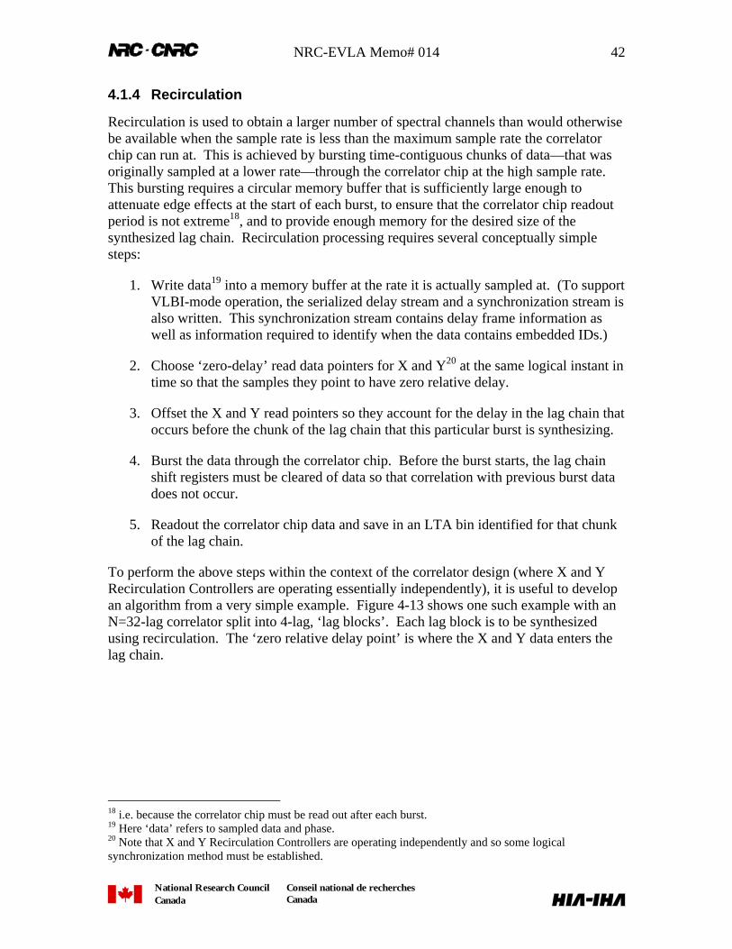
NRC-EVLA Memo# 014 42
National Research CouncilCanada
Conseil national de recherchesCanada
4.1.4 Recirculation
Recirculation is used to obtain a larger number of spectral channels than would otherwisebe available when the sample rate is less than the maximum sample rate the correlatorchip can run at. This is achieved by bursting time-contiguous chunks of data—that wasoriginally sampled at a lower rate—through the correlator chip at the high sample rate.This bursting requires a circular memory buffer that is sufficiently large enough toattenuate edge effects at the start of each burst, to ensure that the correlator chip readoutperiod is not extreme18, and to provide enough memory for the desired size of thesynthesized lag chain. Recirculation processing requires several conceptually simplesteps:
1. Write data19 into a memory buffer at the rate it is actually sampled at. (To supportVLBI-mode operation, the serialized delay stream and a synchronization stream isalso written. This synchronization stream contains delay frame information aswell as information required to identify when the data contains embedded IDs.)
2. Choose ‘zero-delay’ read data pointers for X and Y20 at the same logical instant intime so that the samples they point to have zero relative delay.
3. Offset the X and Y read pointers so they account for the delay in the lag chain thatoccurs before the chunk of the lag chain that this particular burst is synthesizing.
4. Burst the data through the correlator chip. Before the burst starts, the lag chainshift registers must be cleared of data so that correlation with previous burst datadoes not occur.
5. Readout the correlator chip data and save in an LTA bin identified for that chunkof the lag chain.
To perform the above steps within the context of the correlator design (where X and YRecirculation Controllers are operating essentially independently), it is useful to developan algorithm from a very simple example. Figure 4-13 shows one such example with anN=32-lag correlator split into 4-lag, ‘lag blocks’. Each lag block is to be synthesizedusing recirculation. The ‘zero relative delay point’ is where the X and Y data enters thelag chain.
18 i.e. because the correlator chip must be read out after each burst.19 Here ‘data’ refers to sampled data and phase.20 Note that X and Y Recirculation Controllers are operating independently and so some logicalsynchronization method must be established.
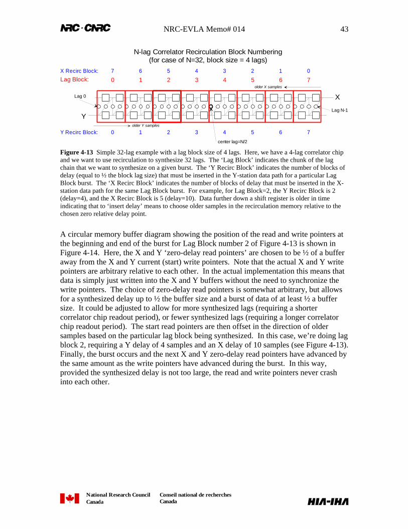
NRC-EVLA Memo# 014 43
National Research CouncilCanada
Conseil national de recherchesCanada
X
Y
Lag Block: 0 1 2 3 4 5 6 7X Recirc Block: 7 6 5 4 3 2 1 0
Y Recirc Block: 0 1 2 3 4 5 6 7
center lag=N/2
Lag 0
Lag N-1
N-lag Correlator Recirculation Block Numbering(for case of N=32, block size = 4 lags)
older Y samples
older X samples
Figure 4-13 Simple 32-lag example with a lag block size of 4 lags. Here, we have a 4-lag correlator chipand we want to use recirculation to synthesize 32 lags. The ‘Lag Block’ indicates the chunk of the lagchain that we want to synthesize on a given burst. The ‘Y Recirc Block’ indicates the number of blocks ofdelay (equal to ½ the block lag size) that must be inserted in the Y-station data path for a particular LagBlock burst. The ‘X Recirc Block’ indicates the number of blocks of delay that must be inserted in the X-station data path for the same Lag Block burst. For example, for Lag Block=2, the Y Recirc Block is 2(delay=4), and the X Recirc Block is 5 (delay=10). Data further down a shift register is older in timeindicating that to ‘insert delay’ means to choose older samples in the recirculation memory relative to thechosen zero relative delay point.
A circular memory buffer diagram showing the position of the read and write pointers atthe beginning and end of the burst for Lag Block number 2 of Figure 4-13 is shown inFigure 4-14. Here, the X and Y ‘zero-delay read pointers’ are chosen to be ½ of a bufferaway from the X and Y current (start) write pointers. Note that the actual X and Y writepointers are arbitrary relative to each other. In the actual implementation this means thatdata is simply just written into the X and Y buffers without the need to synchronize thewrite pointers. The choice of zero-delay read pointers is somewhat arbitrary, but allowsfor a synthesized delay up to ½ the buffer size and a burst of data of at least ½ a buffersize. It could be adjusted to allow for more synthesized lags (requiring a shortercorrelator chip readout period), or fewer synthesized lags (requiring a longer correlatorchip readout period). The start read pointers are then offset in the direction of oldersamples based on the particular lag block being synthesized. In this case, we’re doing lagblock 2, requiring a Y delay of 4 samples and an X delay of 10 samples (see Figure 4-13).Finally, the burst occurs and the next X and Y zero-delay read pointers have advanced bythe same amount as the write pointers have advanced during the burst. In this way,provided the synthesized delay is not too large, the read and write pointers never crashinto each other.
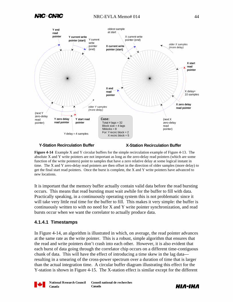
NRC-EVLA Memo# 014 44
National Research CouncilCanada
Conseil national de recherchesCanada
Y current writepointer (start)
Y zero delayread pointer
Y start readpointer
X startreadpointer
X current writepointer (start)
X zero delayread pointer
X current writepointer (end)
X endreadpointer
(next Xzero-delayreadpointer)
X delay=10 samples
Y delay = 4 samples
Y endreadpointer
Y currentwritepointer(end)
(next Yzero-delayreadpointer)
Y-Station Recirculation Buffer X-Station Recirculation Buffer
older X samples(more delay)
oldest sampleat start
Case: Total # lags = 32 Block size = 4 lags Nblocks = 8 For: Y recirc block = 2 X recirc block = 5
older Y samples(more delay)
Figure 4-14 Example X and Y circular buffers for the simple recirculation example of Figure 4-13. Theabsolute X and Y write pointers are not important as long as the zero-delay read pointers (which are somefunction of the write pointers) point to samples that have a zero relative delay at some logical instant intime. The X and Y zero-delay read pointers are then offset in the direction of older samples (more delay) toget the final start read pointers. Once the burst is complete, the X and Y write pointers have advanced tonew locations.
It is important that the memory buffer actually contain valid data before the read burstingoccurs. This means that read bursting must wait awhile for the buffer to fill with data.Practically speaking, in a continuously operating system this is not problematic since itwill take very little real time for the buffer to fill. This makes it very simple: the buffer iscontinuously written to with no need for X and Y write pointer synchronization, and readbursts occur when we want the correlator to actually produce data.
4.1.4.1 Timestamps
In Figure 4-14, an algorithm is illustrated in which, on average, the read pointer advancesat the same rate as the write pointer. This is a robust, simple algorithm that ensures thatthe read and write pointers don’t crash into each other. However, it is also evident thateach burst of data going through the correlator chip occurs on a different time-contiguouschunk of data. This will have the effect of introducing a time skew in the lag data—resulting in a smearing of the cross-power spectrum over a duration of time that is largerthan the actual integration time. A circular buffer diagram illustrating this effect for theY-station is shown in Figure 4-15. The X-station effect is similar except for the different
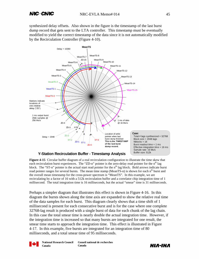
NRC-EVLA Memo# 014 45
National Research CouncilCanada
Conseil national de recherchesCanada
synthesized delay offsets. Also shown in the figure is the timestamp of the last burstdump record that gets sent to the LTA controller. This timestamp must be eventuallymodified to yield the correct timestamp of the data since it is not automatically modifiedby the Recirculation Controller (Figure 4-10).
Y-Station Recirculation Buffer - Timestamp Analysis
Case: Total # lags synthesized = 32768 Block size = 2048 lags Nblocks = 16 Burst readout time = 1 ms Effective integration time = 16 ms Sample rate: 16 Ms/s Buffer size: 512k
MeanTS-0
MeanTS-1
MeanTS-2
MeanTS-15
ST-0ST-1
ST-2ZD-1
ZD-2
ZD-0
ZD-3
ZD-4
ZD-15
MeanTS-14
MeanTS-13MeanTS-3
MeanTS-4
MeanTS-5
MeanTS-6
MeanTS-7MeanTS-8
MeanTS-9MeanTS-10
MeanTS-11
MeanTS-12
MeanTS
1 ms of data@ 16 Ms/s
1 ms output burst:256k samples @256 Ms/s
Location of writepointer when lastburst dump finished:This is the TIMESTAMPof the last burstdump record.
Delay = 15360
Delay = 2048
Markers indicatelocations ofzero relativedelay ("ZD")
Figure 4-15 Circular buffer diagram of a real recirculation configuration to illustrate the time skew thateach recirculation burst experiences. The “ZD-n” pointer is the zero-delay read pointer for the nth lagblock. The “ST-n” pointer is the actual start read pointer for the nth lag block. Bold arrows indicate burstread pointer ranges for several bursts. The mean time stamp (MeanTS-n) is shown for each nth burst andthe overall mean timestamp for the cross-power spectrum is “MeanTS”. In this example, we arerecirculating by a factor of 16 with a 512k recirculation buffer and a correlator chip integration time of 1millisecond. The total integration time is 16 milliseconds, but the actual “smear” time is 31 milliseconds.
Perhaps a simpler diagram that illustrates this effect is shown in Figure 4-16. In thisdiagram the bursts shown along the time axis are expanded to show the relative real timeof the data samples for each burst. This diagram clearly shows that a time shift of 1millisecond is present for each consecutive burst and is for the case where one complete32768-lag result is produced with a single burst of data for each chunk of the lag chain.In this case the total smear time is nearly double the actual integration time. However, ifthe integration time is increased so that many bursts are integrated for one result, thesmear time starts to approach the integration time. This effect is illustrated in Figure4-17. In this example, five bursts are integrated for an integration time of 80milliseconds, and a total smear time of 95 milliseconds.
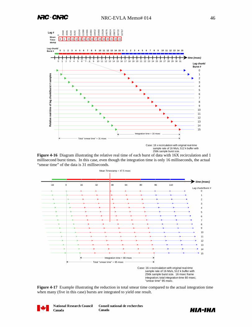
NRC-EVLA Memo# 014 46
National Research CouncilCanada
Conseil national de recherchesCanada
time (msec)
Integration time = 16 msec
0123456789
101112131415
0 1 2 3 4 5 6 7 8 9 10 11 12 13 14 15 16 17 18 19 20 21 22 23 24 25 26 27 28 29 30 31Lag chunk/Burst #
Lag chunk/Burst # 0 1 2 3 4 5 6 7 8 9 10 11 12 13 14 15
Rel
ativ
e re
al-t
ime
of la
g ch
unk/
burs
t # s
ampl
es
Total "smear time" = 31 msec
0 1 2 3 4 5 6 7 8 9 10 11 12 13 14 15
Case: 16 x recirculation with original real-time sample rate of 16 Ms/s, 512 k buffer with 256k sample burst size.
8 9 10 11 12 13 14 15 16 17 18 19 20 21 22 23
Lag #
0 2048
4096
6144
8192
MeanTime-stamp
1024
0
1228
8
1436
6
1638
4
184
32
204
80
225
28
245
76
266
24
286
72
307
20
327
67
Figure 4-16 Diagram illustrating the relative real time of each burst of data with 16X recirculation and 1millisecond burst times. In this case, even though the integration time is only 16 milliseconds, the actual“smear time” of the data is 31 milliseconds.
time (msec)
Integration time = 80 msec
Total "smear time" = 95 msec
0 16 32 48 64 80 96 110-16
0
1
2
3
4
5
6
7
8
9
10
11
12
13
14
15
Lag chunk/Burst #
Mean Timestamp = 47.5 msec
Case: 16 x recirculation with original real-time sample rate of 16 Ms/s, 512 k buffer with 256k sample burst size. 16 msec frame integration; total integration time 80 msec; "smear time" 95 msec.
Figure 4-17 Example illustrating the reduction in total smear time compared to the actual integration timewhen many (five in this case) bursts are integrated to yield one result.
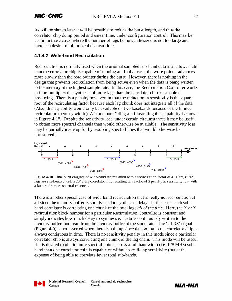
NRC-EVLA Memo# 014 47
National Research CouncilCanada
Conseil national de recherchesCanada
As will be shown later it will be possible to reduce the burst length, and thus thecorrelator chip dump period and smear time, under configuration control. This may beuseful in those cases where the number of lags being synthesized is not too large andthere is a desire to minimize the smear time.
4.1.4.2 Wide-band Recirculation
Recirculation is normally used when the original sampled sub-band data is at a lower ratethan the correlator chip is capable of running at. In that case, the write pointer advancesmore slowly than the read pointer during the burst. However, there is nothing in thedesign that prevents recirculation from being active even when the data is being writtento the memory at the highest sample rate. In this case, the Recirculation Controller worksto time-multiplex the synthesis of more lags than the correlator chip is capable ofproducing. There is a penalty however, in that the reduction in sensitivity is the squareroot of the recirculating factor because each lag chunk does not integrate all of the data.(Also, this capability would only be available on two basebands because of the limitedrecirculation memory width.) A “time burst” diagram illustrating this capability is shownin Figure 4-18. Despite the sensitivity loss, under certain circumstances it may be usefulto obtain more spectral channels than would otherwise be available. The sensitivity lossmay be partially made up for by resolving spectral lines that would otherwise beunresolved.
time (msec)
Lag chunk/Burst # 0 1 2 3 0 1 2 3 0
0...20472048...4095
4096...61436144...8191
0...20472048...4095
4096...61436144...8191
0...2047
0 1 2 3 4 5 6 7 8 9
Figure 4-18 Time burst diagram of wide-band recirculation with a recirculation factor of 4. Here, 8192lags are synthesized with a 2048-lag correlator chip resulting in a factor of 2 penalty in sensitivity, but witha factor of 4 more spectral channels.
There is another special case of wide-band recirculation that is really not recirculation atall since the memory buffer is simply used to synthesize delay. In this case, each sub-band correlator is correlating one chunk of the total lags all of the time. Here, the X or Yrecirculation block number for a particular Recirculation Controller is constant andsimply indicates how much delay to synthesize. Data is continuously written to thememory buffer, and read from the memory buffer at the same rate. The ‘CLRS’ signal(Figure 4-9) is not asserted when there is a dump since data going to the correlator chip isalways contiguous in time. There is no sensitivity penalty in this mode since a particularcorrelator chip is always correlating one chunk of the lag chain. This mode will be usefulif it is desired to obtain more spectral points across a full bandwidth (i.e. 128 MHz) sub-band than one correlator chip is capable of without sacrificing sensitivity (but at theexpense of being able to correlate fewer total sub-bands).
NRC-EVLA Memo# 014 48
National Research CouncilCanada
Conseil national de recherchesCanada
4.1.5 Control and Synchronization Issues
4.1.5.1 Recirculation Real-Time Control
The recirculation algorithm developed in the previous section is simple and robust. Thedata gets written to the circular buffer in a free-wheeling fashion at the original samplerate. Read pointers are a function of the individual write pointers and the desiredsynthesized delay. However, in order for the read pointers in the X and Y RecirculationControllers to be at the correct relative delay, it is necessary to logically synchronizethem to a common reference. Fundamentally, this common reference is TIMECODEsince this signal contains epochs that all events are synchronized to. Practically speakinghowever, it is necessary to not only synchronize the read pointers to some commonepoch, but also provide for a way of telling each of the X and Y recirculation controllerswhat the current lag block (Figure 4-13) is so that the correct synthesized delay can beset. A proposed method of doing this is to use DUMPTRIG for synchronization.DUMPTRIG will synchronize the generation of the X and Y ‘recirculation blocks’(Figure 4-9) within each recirculation controller as well as tell the correlator chip andLTA controller via the dump command (Figure 4-5) where to put the data. Doublechecking of recirculation synchronization can be done on the correlator chip, because itshould detect DUMP_ENn-X and DUMP_ENn-Y pulses at exactly the same instant intime. The steps for recirculation synchronization are as follows:
1. Ensure that all DUMPTRIGs are synchronized to a TIMECODE epoch (the ‘T’bit) within the Recirculation Controllers. Use the dummy DUMPTRIG command‘111’ (synchronization test frame) to do this during initialization and on a periodicbasis21.
2. On each DUMPTRIG dump command, take a snapshot of the write pointer. Add(or subtract) ½ the buffer length to the pointer to form the zero-delay read pointer.This pointer, in the X and Y Recirculation Controllers will point to data with azero relative delay.
3. On each DUMPTRIG dump command, update the recirculation block counter toform the X and Y recirculation block numbers. This number times the size of theblock (in samples of delay) is subtracted from the associated zero-delay readpointer. Always reset the recirculation block counter when the dump command‘100’ is encountered, and on the first occurrence of the ‘010’ command after asequence of ‘000’s or ‘001’s. This will ensure that the counters get reset andresynchronized from time to time.
4. Start the data burst at some time after the dump command—this time must be thesame in X and Y Recirculation Controllers. The data burst will be free-wheelinguntil the next DUMPTRIG dump command (that is not a synchronization test) hascome along. Thus, the period between dump commands determines the duration
21 To allow for hot-swapping a Baseline Board without having to interrupt the operation of other BaselineBoards.
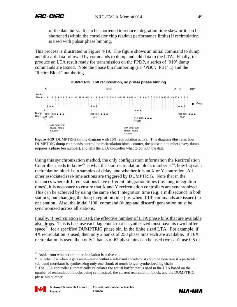
NRC-EVLA Memo# 014 49
National Research CouncilCanada
Conseil national de recherchesCanada
of the data burst. It can be shortened to reduce integration time skew or it can beshortened (within the correlator chip readout performance limits) if recirculationis used with pulsar phase binning.
This process is illustrated in Figure 4-19. The figure shows an initial command to dumpand discard data followed by commands to dump and add data to the LTA. Finally, toproduce an LTA result ready for transmission on the FPDP, a series of ‘010’ dumpcommands are issued. Note the phase bin numbering (i.e. ‘PB0’, ‘PB1’...) and the‘Recirc Block’ numbering.
PB0
time
000000
000 001001
001
0 1 2 3 4 5 6 7 8 9 10 11 12 13 14 15 0 1 2 3 4 5 6 7 8 9 10 11 12 13 14 15 0 1 2 3 4 5 6 7 8 9 10 11 12 13 14 15RecircBlock:
DumpCmd: 100
0 1 2 3
010010
010 000000
PB1
Alw ays resetrecirc. blockcounter.
Alw ays resetrecirc. blockcounter.
000
DUMPTRIG: 16X recirculation, no pulsar phase binning
Figure 4-19 DUMPTRIG timing diagram with 16X recirculation active. This diagram illustrates howDUMPTRIG dump commands control the recirculation block counter, the phase bin number (every dumprequires a phase bin number), and tells the LTA controller what to do with the data.
Using this synchronization method, the only configuration information the RecirculationController needs to know22 is what the start recirculation block number is23, how big eachrecirculation block is in samples of delay, and whether it is an X or Y controller. Allother associated real-time actions are triggered by DUMPTRIG. Note that in theinstances where different stations have different integration times (i.e. long integrationtimes), it is necessary to ensure that X and Y recirculation controllers are synchronized.This can be achieved by using the same short integration time (e.g. 1 millisecond) in bothstations, but changing the long integration time (i.e. when ‘010’ commands are issued) inone station. Also, the initial ‘100’ command (dump and discard) generation must besynchronized across all stations.
Finally, if recirculation is used, the effective number of LTA phase bins that are availablealso drops. This is because each lag chunk that is synthesized must have its own bufferspace24, for a specified DUMPTRIG phase bin, in the finite sized LTA. For example, if4X recirculation is used, then only 2 banks of 250 phase bins each are available. If 16Xrecirculation is used, then only 2 banks of 62 phase bins can be used (we can’t use 0.5 of
22 Aside from whether or not recirculation is active etc.23 i.e. what it is when it gets reset—since within a sub-band correlator it could be non-zero if a particularsub-band correlator is synthesizing only one chunk of much longer synthesized lag chain24 The LTA controller automatically calculates the actual buffer that is used in the LTA based on thenumber of recirculation blocks being synthesized, the current recirculation block, and the DUMPTRIGphase bin number.
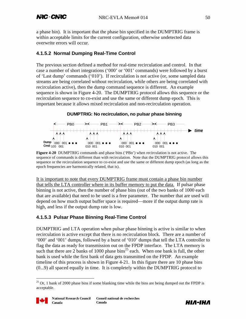
NRC-EVLA Memo# 014 50
National Research CouncilCanada
Conseil national de recherchesCanada
a phase bin). It is important that the phase bin specified in the DUMPTRIG frame iswithin acceptable limits for the current configuration, otherwise undetected dataoverwrite errors will occur.
4.1.5.2 Normal Dumping Real-Time Control
The previous section defined a method for real-time recirculation and control. In thatcase a number of short integrations (‘000’ or ‘001’ commands) were followed by a burstof ‘Last dump’ commands (‘010’). If recirculation is not active (or, some sampled datastreams are being correlated without recirculation, while others are being correlated withrecirculation active), then the dump command sequence is different. An examplesequence is shown in Figure 4-20. The DUMPTRIG protocol allows this sequence or therecirculation sequence to co-exist and use the same or different dump epoch. This isimportant because it allows mixed recirculation and non-recirculation operation.
PB0 PB1 PB2 PB3
time
000001
001100
DumpCmd: 010
000001
001010
000001
001010
000001
001
DUMPTRIG: No recirculation, no pulsar phase binning
Figure 4-20 DUMPTRIG commands and phase bins (‘PBn’) when recirculation is not active. Thesequence of commands is different than with recirculation. Note that the DUMPTRIG protocol allows thissequence or the recirculation sequence to co-exist and use the same or different dump epoch (as long as theepoch frequencies are harmonically related, that is).
It is important to note that every DUMPTRIG frame must contain a phase bin numberthat tells the LTA controller where in its buffer memory to put the data. If pulsar phasebinning is not active, then the number of phase bins (out of the two banks of 1000 eachthat are available) that need to be used is a free parameter. The number that are used willdepend on how much output buffer space is required—more if the output dump rate ishigh, and less if the output dump rate is low.
4.1.5.3 Pulsar Phase Binning Real-Time Control
DUMPTRIG and LTA operation when pulsar phase binning is active is similar to whenrecirculation is active except that there is no recirculation block. There are a number of‘000’ and ‘001’ dumps, followed by a burst of ‘010’ dumps that tell the LTA controller toflag the data as ready for transmission out on the FPDP interface. The LTA memory issuch that there are 2 banks of 1000 phase bins25 each. When one bank is full, the otherbank is used while the first bank of data gets transmitted on the FPDP. An exampletimeline of this process is shown in Figure 4-21. In this figure there are 10 phase bins(0...9) all spaced equally in time. It is completely within the DUMPTRIG protocol to
25 Or, 1 bank of 2000 phase bins if some blanking time while the bins are being dumped out the FPDP isacceptable.
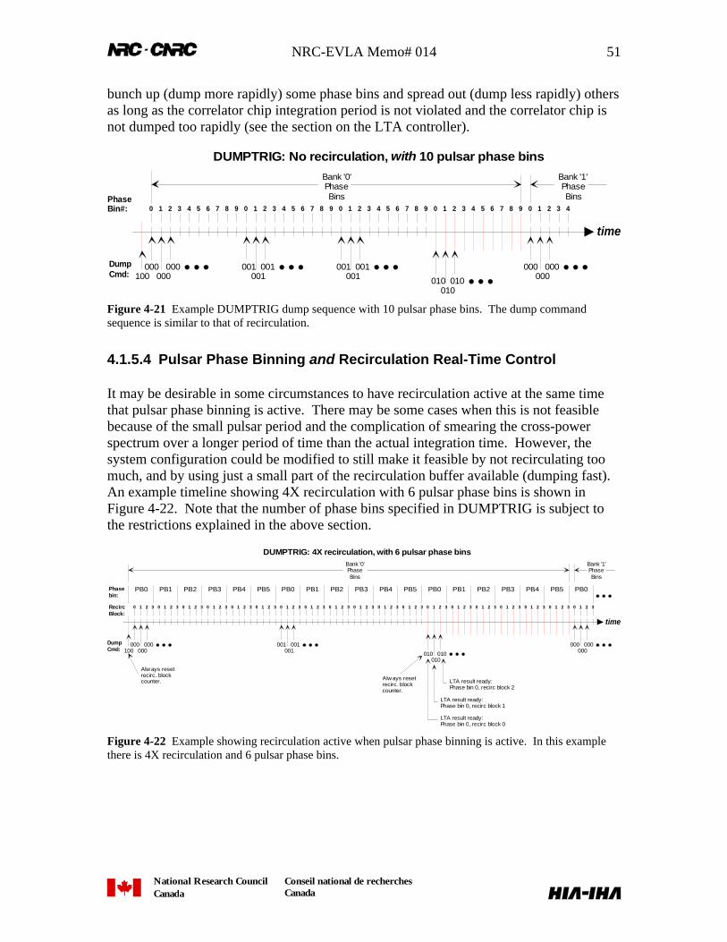
NRC-EVLA Memo# 014 51
National Research CouncilCanada
Conseil national de recherchesCanada
bunch up (dump more rapidly) some phase bins and spread out (dump less rapidly) othersas long as the correlator chip integration period is not violated and the correlator chip isnot dumped too rapidly (see the section on the LTA controller).
time
Bank '1'PhaseBins
000000
000
PhaseBin#: 0 1 2 3 4 5 6 7 8 9 0 1 2 3 4 5 6 7 8 9 0 1 2 3 4 5 6 7 8 9 0 1 2 3 4 5 6 7 8 9
100DumpCmd:
001001
001 001001
001
010010
010
0 1 2 3 4
000000
000
Bank '0'PhaseBins
DUMPTRIG: No recirculation, with 10 pulsar phase bins
Figure 4-21 Example DUMPTRIG dump sequence with 10 pulsar phase bins. The dump commandsequence is similar to that of recirculation.
4.1.5.4 Pulsar Phase Binning and Recirculation Real-Time Control
It may be desirable in some circumstances to have recirculation active at the same timethat pulsar phase binning is active. There may be some cases when this is not feasiblebecause of the small pulsar period and the complication of smearing the cross-powerspectrum over a longer period of time than the actual integration time. However, thesystem configuration could be modified to still make it feasible by not recirculating toomuch, and by using just a small part of the recirculation buffer available (dumping fast).An example timeline showing 4X recirculation with 6 pulsar phase bins is shown inFigure 4-22. Note that the number of phase bins specified in DUMPTRIG is subject tothe restrictions explained in the above section.
PB0
time
000000
000
0 1 2 3RecircBlock:
DumpCmd: 100
Alw ays resetrecirc. blockcounter.
Alw ays resetrecirc. blockcounter.
DUMPTRIG: 4X recirculation, with 6 pulsar phase bins
0 1 2 3
PB1
0 1 2 3
PB2
0 1 2 3
PB3
0 1 2 3
PB4
0 1 2 3
PB5 PB0
0 1 2 3 0 1 2 3
PB1
0 1 2 3
PB2
0 1 2 3
PB3
0 1 2 3
PB4
0 1 2 3
PB5
001001
001
0 1 2 3 0 1 2 3 0 1 2 3 0 1 2 3 0 1 2 3 0 1 2 3
010010
010
PB0 PB1 PB2 PB3 PB4 PB5
0 1 2 3
PB0
000000
000
LTA result ready:Phase bin 0, recirc block 0
LTA result ready:Phase bin 0, recirc block 1
LTA result ready:Phase bin 0, recirc block 2
Phasebin:
Bank '0'PhaseBins
Bank '1'PhaseBins
Figure 4-22 Example showing recirculation active when pulsar phase binning is active. In this examplethere is 4X recirculation and 6 pulsar phase bins.
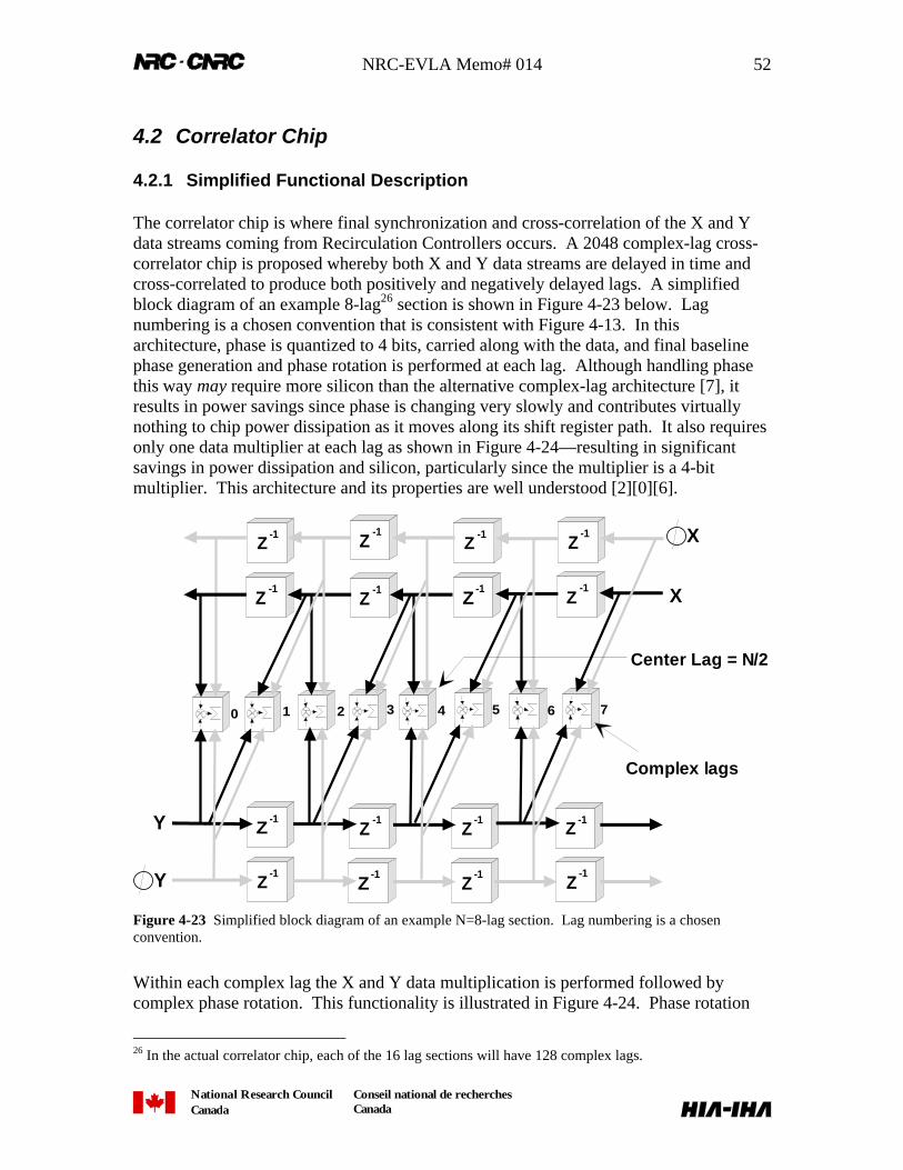
NRC-EVLA Memo# 014 52
National Research CouncilCanada
Conseil national de recherchesCanada
4.2 Correlator Chip
4.2.1 Simplified Functional Description
The correlator chip is where final synchronization and cross-correlation of the X and Ydata streams coming from Recirculation Controllers occurs. A 2048 complex-lag cross-correlator chip is proposed whereby both X and Y data streams are delayed in time andcross-correlated to produce both positively and negatively delayed lags. A simplifiedblock diagram of an example 8-lag26 section is shown in Figure 4-23 below. Lagnumbering is a chosen convention that is consistent with Figure 4-13. In thisarchitecture, phase is quantized to 4 bits, carried along with the data, and final baselinephase generation and phase rotation is performed at each lag. Although handling phasethis way may require more silicon than the alternative complex-lag architecture [7], itresults in power savings since phase is changing very slowly and contributes virtuallynothing to chip power dissipation as it moves along its shift register path. It also requiresonly one data multiplier at each lag as shown in Figure 4-24—resulting in significantsavings in power dissipation and silicon, particularly since the multiplier is a 4-bitmultiplier. This architecture and its properties are well understood [2][0][6].
Z-1
Z-1
Z-1
Z-1
Z-1
Z-1
Z-1
Z-1
Z-1
Z-1
Z-1
Z-1
Z-1
Z-1
Z-1
Z-1
Y
Y
X
X
4321 5 6 70
Complex lags
Center Lag = N/2
Figure 4-23 Simplified block diagram of an example N=8-lag section. Lag numbering is a chosenconvention.
Within each complex lag the X and Y data multiplication is performed followed bycomplex phase rotation. This functionality is illustrated in Figure 4-24. Phase rotation
26 In the actual correlator chip, each of the 16 lag sections will have 128 complex lags.
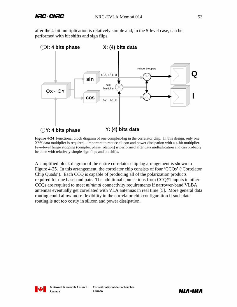
NRC-EVLA Memo# 014 53
National Research CouncilCanada
Conseil national de recherchesCanada
after the 4-bit multiplication is relatively simple and, in the 5-level case, can beperformed with bit shifts and sign flips.
X - Y
sin
cos
Q
I
X: (4) bits dataX: 4 bits phase
Y: 4 bits phase Y: (4) bits data
+/-2, +/-1, 0
+/-2, +/-1, 0
DataMultiplier
Fringe Stoppers
Figure 4-24 Functional block diagram of one complex-lag in the correlator chip. In this design, only oneX*Y data multiplier is required—important to reduce silicon and power dissipation with a 4-bit multiplier.Five-level fringe stopping (complex phase rotation) is performed after data multiplication and can probablybe done with relatively simple sign flips and bit shifts.
A simplified block diagram of the entire correlator chip lag arrangement is shown inFigure 4-25. In this arrangement, the correlator chip consists of four ‘CCQs’ (‘CorrelatorChip Quads’). Each CCQ is capable of producing all of the polarization productsrequired for one baseband pair. The additional connections from CCQ#1 inputs to otherCCQs are required to meet minimal connectivity requirements if narrower-band VLBAantennas eventually get correlated with VLA antennas in real time [5]. More general datarouting could allow more flexibility in the correlator chip configuration if such datarouting is not too costly in silicon and power dissipation.
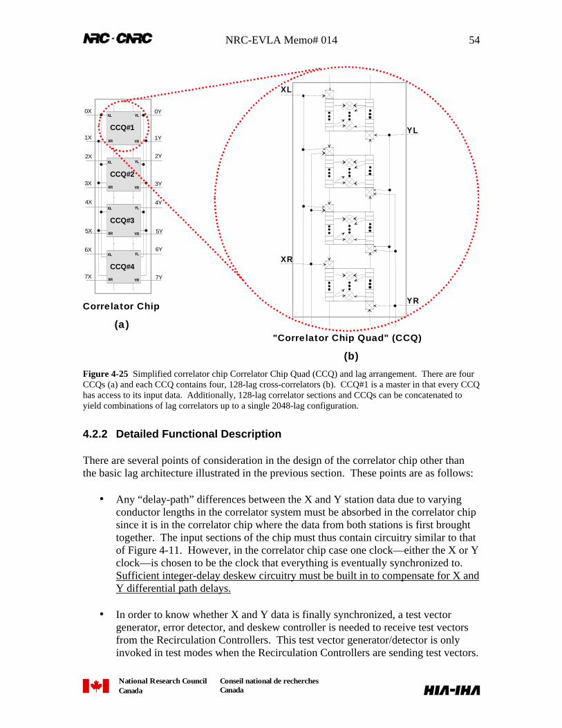
NRC-EVLA Memo# 014 54
National Research CouncilCanada
Conseil national de recherchesCanada
XL
XR
YL
YR
XL
XR
YL
YR
CCQ#1
XL
XR
YL
YR
CCQ#2
XL
XR
YL
YR
CCQ#3
XL
XR
YL
YR
CCQ#4
1X
3X
4X
5X
6X
2X
7X
1Y
2Y
3Y
4Y
5Y
6Y
7Y
0X 0Y
"Correlator Chip Quad" (CCQ)
Correlator Chip
(a)
(b)Figure 4-25 Simplified correlator chip Correlator Chip Quad (CCQ) and lag arrangement. There are fourCCQs (a) and each CCQ contains four, 128-lag cross-correlators (b). CCQ#1 is a master in that every CCQhas access to its input data. Additionally, 128-lag correlator sections and CCQs can be concatenated toyield combinations of lag correlators up to a single 2048-lag configuration.
4.2.2 Detailed Functional Description
There are several points of consideration in the design of the correlator chip other thanthe basic lag architecture illustrated in the previous section. These points are as follows:
• Any “delay-path” differences between the X and Y station data due to varyingconductor lengths in the correlator system must be absorbed in the correlator chipsince it is in the correlator chip where the data from both stations is first broughttogether. The input sections of the chip must thus contain circuitry similar to thatof Figure 4-11. However, in the correlator chip case one clock—either the X or Yclock—is chosen to be the clock that everything is eventually synchronized to.Sufficient integer-delay deskew circuitry must be built in to compensate for X andY differential path delays.
• In order to know whether X and Y data is finally synchronized, a test vectorgenerator, error detector, and deskew controller is needed to receive test vectorsfrom the Recirculation Controllers. This test vector generator/detector is onlyinvoked in test modes when the Recirculation Controllers are sending test vectors.
NRC-EVLA Memo# 014 55
National Research CouncilCanada
Conseil national de recherchesCanada
In normal (“on-the-sky”) operation, the input circuitry must detect errors bylooking for protocol violations and signal “eyes” as shown in the timing diagramof Figure 4-9.
• The correlator chip does not know much about recirculation. The only cues itgets are the ‘CLRS’ bit and holdoff in a particular DUMP_EN line and theRECIRC_BLK line associated with each dump. The CLRS bit simply tells thecorrelator chip that it is to clear the output of associated lag shift registers, holdoffprevents the chip from correlating until it is negated, and the RECIRC_BLK iscaptured and passed on to the LTA controller in the correlator chip output dataframe.
• Based on internal switch settings, and X-station/Y-station selection, the correlatorchip must route each DUMP_EN line to a particular set of lags in a particularCCQ. When recirculation is active, associated DUMP_EN lines from the X andY Recirculation Controllers must be asserted coincidentally (once synchronizedon the correlator chip). This is because dumping controls recirculation countersand pointers in the Recirculation Controllers. The correlator chip should bedesigned to check for this synchronization.
• Each set of 128 lags operates independently as far as dumping goes. Each set oflags has its own independent output data frame that is treated independently bythe LTA controller.
• Dump overruns, where data has not been read out before another dump signalcomes along, must be properly handled in the correlator chip. It is suggested thatwhen a dump overrun occurs, existing data waiting to be read out is notdisturbed—rather new data is discarded, and a status bit is set to indicate that oneor more data dumps were discarded.
4.2.2.1 Black-Box Correlator Chip Diagram
A black-box diagram of the correlator chip is shown in Figure 4-26. In the figure, thereare identical X and Y inputs, an LTA controller interface for data output, and a Monitorand Control Bus (MCB) interface for configuration and status monitoring. In this designthere is no provision for allowing multiple correlator chips to be concatenated since thisrequires more I/O, is probably somewhat more costly, and is not a requirement for theEVLA27. However, when the chip is actually developed, this possibility should beconsidered since it results in a more general device (although it may be impossible to dobecause of synchronization, time-skew concerns, and increased die size and cost).
27 i.e. to be able to tradeoff number of baselines processed for spectral resolution.
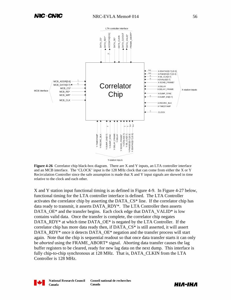
NRC-EVLA Memo# 014 56
National Research CouncilCanada
Conseil national de recherchesCanada
8x4X-SDATAO[0:7]-[0:3]
8x4 X-PHASEO[0:7]-[0:3]8
X-SE_CLK[0:7]8
X-DVALID[0:7]
CLOCK
8X-DUMP_EN[0:7]
X-DELAYX-DELAY_FRAME
X-RECIRC_BLK
X-TIMESTAMP
X-SCHID_FRAME*
2
X-DUMP_SYNC
8x4
Y-S
DA
TAO
[0:7
]-[0
:3]
8x4
Y-P
HA
SE
O[0
:7]-
[0:3
]8
Y-S
E_C
LK[0
:7]
8Y
-DV
ALI
D[0
:7]
8Y
-DU
MP
_EN
[0:7
]
Y-D
ELA
YY
-DE
LAY
_FR
AM
E
Y-R
EC
IRC
_BLK
Y-T
IME
STA
MP
Y-S
CH
ID_F
RA
ME
*
Y-D
UM
P_S
YN
C
MCB_ADDR[0:6]MCB_DATA[0:7]
MCB_CS*MCB_RD*
MCB_CLK
7
8 CorrelatorChip
X-station inputs
Y-station inputs
DA
TA
_RD
Y*
AC
CD
ATA
[0:3
1]
32
DA
TA
_OE
*
DA
TA_C
LKIN
DA
TA
_CLK
OU
T
MCB interface
LTA controller interface
DA
TA
_VA
LID
*
MCB_WR*
DA
TA
_CS
*
FRA
ME
_AB
OR
T*
Figure 4-26 Correlator chip black-box diagram. There are X and Y inputs, an LTA controller interfaceand an MCB interface. The ‘CLOCK’ input is the 128 MHz clock that can come from either the X or YRecirculation Controller since the safe assumption is made that X and Y input signals are skewed in timerelative to the clock and each other.
X and Y station input functional timing is as defined in Figure 4-9. In Figure 4-27 below,functional timing for the LTA controller interface is defined. The LTA Controlleractivates the correlator chip by asserting the DATA_CS* line. If the correlator chip hasdata ready to transmit, it asserts DATA_RDY*. The LTA Controller then assertsDATA_OE* and the transfer begins. Each clock edge that DATA_VALID* is lowcontains valid data. Once the transfer is complete, the correlator chip negatesDATA_RDY* at which time DATA_OE* is negated by the LTA Controller. If thecorrelator chip has more data ready then, if DATA_CS* is still asserted, it will assertDATA_RDY* once it detects DATA_OE* negation and the transfer process will startagain. Note that the chip is sequential readout so that once data transfer starts it can onlybe aborted using the FRAME_ABORT* signal. Aborting data transfer causes the lagbuffer registers to be cleared, ready for new lag data on the next dump. This interface isfully chip-to-chip synchronous at 128 MHz. That is, DATA_CLKIN from the LTAController is 128 MHz.
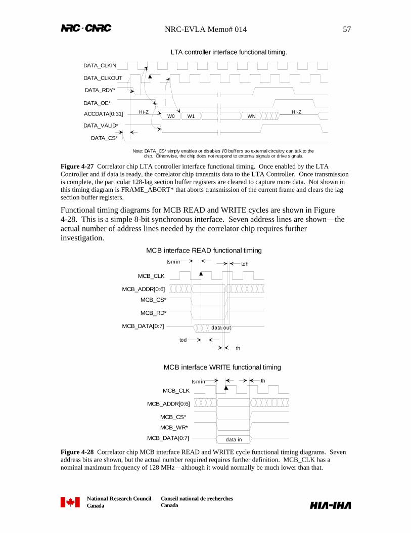
NRC-EVLA Memo# 014 57
National Research CouncilCanada
Conseil national de recherchesCanada
DATA_CLKOUT
DATA_RDY*
DATA_CLKIN
DATA_OE*
W0 W1ACCDATA[0:31] WN
LTA controller interface functional timing.
Hi-Z Hi-Z
DATA_VALID*
DATA_CS*
Note: DATA_CS* simply enables or disables I/O buffers so external circuitry can talk to the chip. Otherw ise, the chip does not respond to external signals or drive signals.
Figure 4-27 Correlator chip LTA controller interface functional timing. Once enabled by the LTAController and if data is ready, the correlator chip transmits data to the LTA Controller. Once transmissionis complete, the particular 128-lag section buffer registers are cleared to capture more data. Not shown inthis timing diagram is FRAME_ABORT* that aborts transmission of the current frame and clears the lagsection buffer registers.
Functional timing diagrams for MCB READ and WRITE cycles are shown in Figure4-28. This is a simple 8-bit synchronous interface. Seven address lines are shown—theactual number of address lines needed by the correlator chip requires furtherinvestigation.
MCB_CLK
MCB_ADDR[0:6]
MCB_CS*
MCB_RD*
MCB_DATA[0:7] data out
MCB interface READ functional timing
tsm in
tod
toh
th
MCB_CLK
MCB_ADDR[0:6]
MCB_CS*
MCB_WR*
MCB_DATA[0:7] data in
tsm in th
MCB interface WRITE functional timing
Figure 4-28 Correlator chip MCB interface READ and WRITE cycle functional timing diagrams. Sevenaddress bits are shown, but the actual number required requires further definition. MCB_CLK has anominal maximum frequency of 128 MHz—although it would normally be much lower than that.
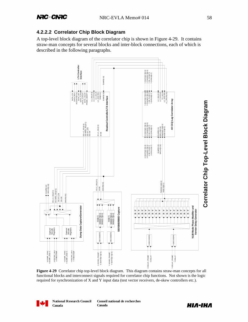
NRC-EVLA Memo# 014 58
National Research CouncilCanada
Conseil national de recherchesCanada
4.2.2.2 Correlator Chip Block DiagramA top-level block diagram of the correlator chip is shown in Figure 4-29. It containsstraw-man concepts for several blocks and inter-block connections, each of which isdescribed in the following paragraphs.
X-D
UM
P_
SY
NC
X-D
UM
P_
EN
[0:7
]
X-R
EC
IRC
_BLK
X-T
IME
ST
AM
P
Y-D
UM
P_
SY
NC
Y-D
UM
P_
EN
[0:7
]
Y-R
EC
IRC
_B
LK
Y-T
IME
ST
AM
P
DU
MP
[0:1
5]
SR
CL
R[0
:15
]
DG
-LC
_S
EL
[0:3
]
DG
-WR
D_
SE
L[0
:1]
Cap
ture
/D
ecod
eR
egis
ters
Cap
ture
/D
ecod
eR
egis
ters
DG
-X/Y
_E
N
DO
UT
[0:3
1]
DG
-OE
Dum
p D
ata
Cap
ture
/Gen
erat
or
DE
CO
DE
RS
SID
[0:7
]S
BID
[0:7
][0:4
]B
BID
[0:7
][0:3
]Y
-SD
AT
A[0
:7][
0:3
]
Y-S
CH
ID_
FR
AM
E*
DE
CO
DE
RS
SID
[0:7
]S
BID
[0:7
][0:4
]B
BID
[0:7
][0:3
]X
-SD
AT
A[0
:7][
0:3
]
X-S
CH
ID_
FR
AM
E*
SID
/SB
ID/B
BID
Cap
ture
ID-L
C_
SE
L[0
:3]
ID-O
E
DO
UT
[0:3
1]
X-D
EC
OD
ER
S
X -
Y
X -
Y
X -
Y
X -
Y
X -
Y
X -
Y
X -
Y
X -
Y
X -
Y
X -
Y
X -
Y
X -
Y
X -
Y
X -
Y
X -
Y
X -
Y
Y-D
EC
OD
ER
S
X-D
EL
AY
_F
RA
ME
X-D
EL
AY
Y-D
EL
AY
_F
RA
ME
Y-D
EL
AY
PM
OD
[0:1
5][
0:3
]
VD
[0:1
5][
0:1
]
VLB
I Mod
e P
hase
Mod
ifier
and
Ver
nier
Del
ay G
ener
ator
X-S
DA
TA
[0:7
][0
:3]
X-P
HA
SE
[0:7
][0
:3]
X-S
E_
CL
K[0
:7]
X-D
VA
LID
[0:7
]
DU
MP
[0:1
5]
SR
CL
R[0
:15
]P
MO
D[0
:15
][0
:3]
VD
[0:1
5][
0:1
]
Y-S
DA
TA
[0:7
][0
:3]
Y-P
HA
SE
[0:7
][0
:3]
Y-S
E_
CL
K[0
:7]
Y-D
VA
LID
[0:7
]
LC
_S
EL
[0:3
]L
C_
ST
AT
US
LC
_D
CL
RL
C_
DO
UT
EN
LC
_D
OU
T[0
:31
]
4X C
CQ
Lag
Cor
rela
tor
Arr
ayDU
MP
[0:1
5]
LC
_S
EL
[0:3
]L
C_
ST
AT
US
LC
_D
CL
RL
C_
DO
UT
EN
DIN
[0:3
1]
Rea
dout
Con
trol
ler/
LTA
Inte
rfac
e
ID-L
C_
SE
L[0
:3]
ID-O
E
DG
-LC
_S
EL
[0:3
]D
G-W
RD
_SE
L[0:
1]D
G-X
/Y_E
ND
G-O
E
DU
MP
[0:1
5]
DU
MP
[0:1
5]
SR
CL
R[0
:15
]
X-S
DA
TA
[0:7
][0
:3]
X-P
HA
SE
[0:7
][0
:3]
X-S
E_
CL
K[0
:7]
X-D
VA
LID
[0:7
]
Y-S
DA
TA
[0:7
][0
:3]
Y-P
HA
SE
[0:7
][0
:3]
Y-S
E_
CL
K[0
:7]
Y-D
VA
LID
[0:7
]
DA
TA
_C
S*
DA
TA
_R
DY
*A
CC
DA
TA
[0:3
1]
DA
TA
_O
E*
DA
TA
_C
LK
IND
AT
A_
CL
KO
UT
DA
TA
_V
AL
ID*
FR
AM
E_
AB
OR
T*
LTA
Co
ntro
ller
Inte
rfac
e
Cor
rela
tor
Chi
p To
p-Le
vel B
lock
Dia
gram
Figure 4-29 Correlator chip top-level block diagram. This diagram contains straw-man concepts for allfunctional blocks and interconnect signals required for correlator chip functions. Not shown is the logicrequired for synchronization of X and Y input data (test vector receivers, de-skew controllers etc.).
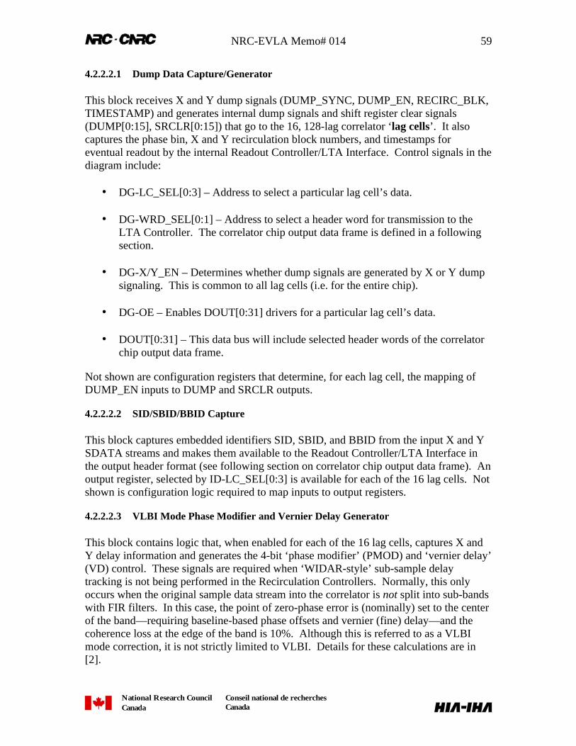
NRC-EVLA Memo# 014 59
National Research CouncilCanada
Conseil national de recherchesCanada
4.2.2.2.1 Dump Data Capture/Generator
This block receives X and Y dump signals (DUMP_SYNC, DUMP_EN, RECIRC_BLK,TIMESTAMP) and generates internal dump signals and shift register clear signals(DUMP[0:15], SRCLR[0:15]) that go to the 16, 128-lag correlator ‘lag cells’. It alsocaptures the phase bin, X and Y recirculation block numbers, and timestamps foreventual readout by the internal Readout Controller/LTA Interface. Control signals in thediagram include:
• DG-LC_SEL[0:3] – Address to select a particular lag cell’s data.
• DG-WRD_SEL[0:1] – Address to select a header word for transmission to theLTA Controller. The correlator chip output data frame is defined in a followingsection.
• DG-X/Y_EN – Determines whether dump signals are generated by X or Y dumpsignaling. This is common to all lag cells (i.e. for the entire chip).
• DG-OE – Enables DOUT[0:31] drivers for a particular lag cell’s data.
• DOUT[0:31] – This data bus will include selected header words of the correlatorchip output data frame.
Not shown are configuration registers that determine, for each lag cell, the mapping ofDUMP_EN inputs to DUMP and SRCLR outputs.
4.2.2.2.2 SID/SBID/BBID Capture
This block captures embedded identifiers SID, SBID, and BBID from the input X and YSDATA streams and makes them available to the Readout Controller/LTA Interface inthe output header format (see following section on correlator chip output data frame). Anoutput register, selected by ID-LC_SEL[0:3] is available for each of the 16 lag cells. Notshown is configuration logic required to map inputs to output registers.
4.2.2.2.3 VLBI Mode Phase Modifier and Vernier Delay Generator
This block contains logic that, when enabled for each of the 16 lag cells, captures X andY delay information and generates the 4-bit ‘phase modifier’ (PMOD) and ‘vernier delay’(VD) control. These signals are required when ‘WIDAR-style’ sub-sample delaytracking is not being performed in the Recirculation Controllers. Normally, this onlyoccurs when the original sample data stream into the correlator is not split into sub-bandswith FIR filters. In this case, the point of zero-phase error is (nominally) set to the centerof the band—requiring baseline-based phase offsets and vernier (fine) delay—and thecoherence loss at the edge of the band is 10%. Although this is referred to as a VLBImode correction, it is not strictly limited to VLBI. Details for these calculations are in[2].
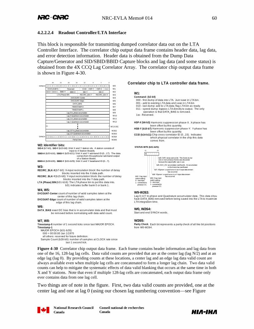
NRC-EVLA Memo# 014 60
National Research CouncilCanada
Conseil national de recherchesCanada
4.2.2.2.4 Readout Controller/LTA Interface
This block is responsible for transmitting dumped correlator data out on the LTAController Interface. The correlator chip output data frame contains header data, lag data,and error detection information. Header data is obtained from the Dump DataCapture/Generator and SID/SBID/BBID Capture blocks and lag data (and some status) isobtained from the 4X CCQ Lag Correlator Array. The correlator chip output data frameis shown in Figure 4-30.
0481216202428
1 0 1 0 1 0 1 0 1 0 1 0 1 0 1 0 1 0 1 0 1 0 1 0 1 0 1 0 1 0 1 0
SID-XSID-YSBID-XSBID-YBBID-XBBID-Y
CmmdHSP-XHSP-YCCIDSTATUS BITS Reserved
RECIRC_BLK-XRECIRC_BLK-YLTA (Phase) BIN
DVCOUNT-Center
DVCOUNT-Edge
DATA_BIAS
TIMESTAMP-0
TIMESTAMP-1
SYNCH
Lag 0-In_phase accumulator
Lag 0-Quadrature accumulator
Lag 1-In_phase accumulator
Lag 1-Quadrature accumulator
Lag 127-In_phase accumulator
Lag 127-Quadrature accumulator
0 0 0 1 1 1 0 0 0 0 0 0 0 0 0 0 0 0 0 01 1 1 1 1 1 1 1 1 1 1 1
Parity Check
W0
W1
W2
W3
W4
W5
W6
W7
W8W9
W10
W11
W12
W264
W265
W263
W262
W13-261
SYNCH
2531
b25: OVR: dump overrun bit. This frame ok, butone or more previous frames was discardedbecause the output buffer was in use.
b27: XSyncerr: a synch error in an X input data stream has occurred.
b26: ACC_OV: accumulator overflow bit. An accumulator in this frame has overflowed.
b28: YSyncerr: a synch error in a Y input data stream has occurred.
b29: X lag inputswitch setting:0 - new input1 - connected to previous CC.
b30: Y lag inputswitch setting:0 - new input1 - connected to previous CC.
STATUS BITS (b31-b25):
x
W1:Command: (b2-b0) 000 - firs t dump of data into LTA. Just save in LTA bin. 001 - add to exis ting LTA data and save in LTA bin. 010 - las t dump: add to LTA data; flag LTA bin as ready. 011 - speed dum p: bypass LTA directly to output. The only operation is that DATA_BIAS is rem oved. 1xx - Reserved.
HSP-X (b6-b3): Harmonic suppress ion phase-X. X-phase has been offset by this quantity.HSB-Y (b10-b7): Harm onic suppress ion phase-Y. Y-phase has been offset by this quantity.CCID (b14-b11): Chip cross-correlator ID (0...15). Indicates which phys ical correlator in the chip this data comes from.
W2: Identifier bits:SID-X (b7-b0), SID-Y (b15-b8): 8-bit X and Y station ids. A station consists of input to 4 Station Boards.SBID-X (b20-b16), SBID-Y (b25-b21): 5-bit X and Y sub-band ID (0...17). The data comes from this particular sub-band output of a Station Board.BBID-X (b28-b26), BBID-Y (b31-b29); 3-bit X and Y baseband ID (0...7).
W3:RECIRC_BLK-X (b7-b0): X-input recirculation block: the number of delay blocks inserted into the X data path.RECIRC_BLK-Y (b15-b8): Y-input recirculation block: the number of delay blocks inserted into the Y data path.LTA (Phase) BIN (b31-b16): The LTA phase bin to put this data into. b31 indicates buffer bank 0 or bank 1.
W4, W5:DVCOUNT-Center: count of num ber of valid samples taken at the center of this lag chain.DVCOUNT-Edge: count of number of valid sam ples taken at the edge of this lag chain.
W6:DATA_BIAS: exact DC bias that is in accumulator data and that must be removed before norm alizing with data valid count.
W7, W8:Timestamp-0: number of 1 second ticks s ince las t MAJOR EPOCH.Timestamp-1: MAJOR EPOCH (b31-b29): 000 = 00:00:00 Jan 1/1970 all others : reserved for future definition. Sam ple Count (b28-b0): num ber of sam ples at CLOCK rate s ince las t 1 second tick.
W9-W263:Lag 0-127 In-phase and Quadrature accum ulator data. This data shouhave DATA_BIAS rem oved before being saved into the LTA to m axim izeLTA integration time.
W0, W264:Start and end SYNCH words .
W265:Parity Check. Each bit represents a parity check of all like bit pos itionsfrom W0-W264.
Correlator chip to LTA controller data frame.
Figure 4-30 Correlator chip output data frame. Each frame contains header information and lag data fromone of the 16, 128-lag lag cells. Data valid counts are provided that are at the center lag (lag N/2) and at anedge lag (lag 0). By providing counts at these locations, a center lag and an edge lag data valid count arealways available even when multiple lag cells are concatenated to form a longer lag chain. Two data validcounts can help to mitigate the systematic effects of data valid blanking that occurs at the same time in bothX and Y stations. Note that even if multiple 128-lag cells are concatenated, each output data frame onlyever contains data from one lag cell.
Two things are of note in the figure. First, two data valid counts are provided, one at thecenter lag and one at lag 0 (using our chosen lag numbering convention—see Figure
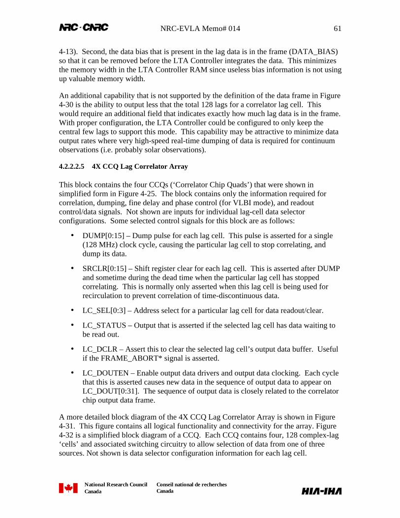
NRC-EVLA Memo# 014 61
National Research CouncilCanada
Conseil national de recherchesCanada
4-13). Second, the data bias that is present in the lag data is in the frame (DATA_BIAS)so that it can be removed before the LTA Controller integrates the data. This minimizesthe memory width in the LTA Controller RAM since useless bias information is not usingup valuable memory width.
An additional capability that is not supported by the definition of the data frame in Figure4-30 is the ability to output less that the total 128 lags for a correlator lag cell. Thiswould require an additional field that indicates exactly how much lag data is in the frame.With proper configuration, the LTA Controller could be configured to only keep thecentral few lags to support this mode. This capability may be attractive to minimize dataoutput rates where very high-speed real-time dumping of data is required for continuumobservations (i.e. probably solar observations).
4.2.2.2.5 4X CCQ Lag Correlator Array
This block contains the four CCQs (‘Correlator Chip Quads’) that were shown insimplified form in Figure 4-25. The block contains only the information required forcorrelation, dumping, fine delay and phase control (for VLBI mode), and readoutcontrol/data signals. Not shown are inputs for individual lag-cell data selectorconfigurations. Some selected control signals for this block are as follows:
• DUMP[0:15] – Dump pulse for each lag cell. This pulse is asserted for a single(128 MHz) clock cycle, causing the particular lag cell to stop correlating, anddump its data.
• SRCLR[0:15] – Shift register clear for each lag cell. This is asserted after DUMPand sometime during the dead time when the particular lag cell has stoppedcorrelating. This is normally only asserted when this lag cell is being used forrecirculation to prevent correlation of time-discontinuous data.
• LC_SEL[0:3] – Address select for a particular lag cell for data readout/clear.
• LC_STATUS – Output that is asserted if the selected lag cell has data waiting tobe read out.
• LC_DCLR – Assert this to clear the selected lag cell’s output data buffer. Usefulif the FRAME_ABORT* signal is asserted.
• LC_DOUTEN – Enable output data drivers and output data clocking. Each cyclethat this is asserted causes new data in the sequence of output data to appear onLC_DOUT[0:31]. The sequence of output data is closely related to the correlatorchip output data frame.
A more detailed block diagram of the 4X CCQ Lag Correlator Array is shown in Figure4-31. This figure contains all logical functionality and connectivity for the array. Figure4-32 is a simplified block diagram of a CCQ. Each CCQ contains four, 128 complex-lag‘cells’ and associated switching circuitry to allow selection of data from one of threesources. Not shown is data selector configuration information for each lag cell.
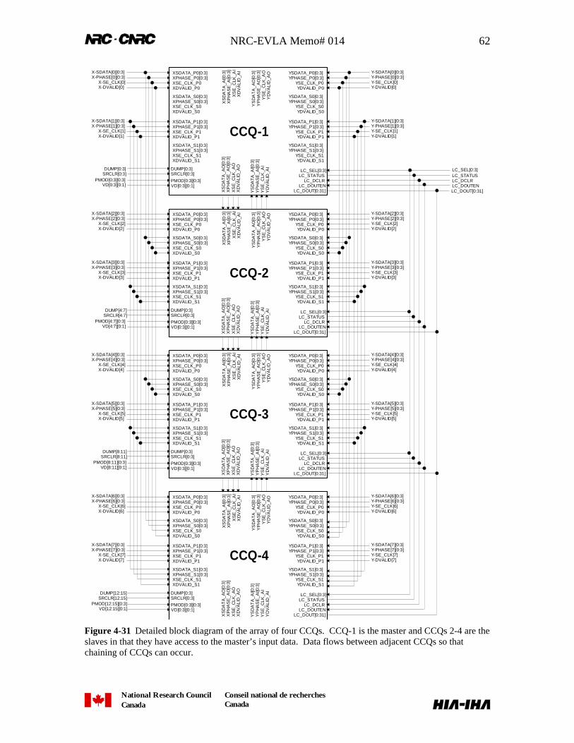
NRC-EVLA Memo# 014 62
National Research CouncilCanada
Conseil national de recherchesCanada
CCQ-1
X-SDATA[0][0:3] Y-SDATA[0][0:3]X-PHASE[0][0:3] Y-PHASE[0][0:3]
PMOD[0:3][0:3]VD[0:3][0:1]
X-SE_CLK[0] Y-SE_CLK[0]Y-DVALID[0]X-DVALID[0]
Y-SDATA[1][0:3]Y-PHASE[1][0:3]Y-SE_CLK[1]Y-DVALID[1]
X-SDATA[1][0:3]X-PHASE[1][0:3]
X-SE_CLK[1]X-DVALID[1]
DUMP[0:3]SRCLR[0:3]
LC_SEL[0:3]
LC_DOUTENPMOD[0:3][0:3]VD[0:3][0:1]
LC_SEL[0:3]
LC_DOUTEN
DUMP[0:3]SRCLR[0:3]
XSDATA_P0[0:3]XPHASE_P0[0:3]XSE_CLK_P0XDVALID_P0
XSDATA_S0[0:3]XPHASE_S0[0:3]XSE_CLK_S0XDVALID_S0
XSDATA_P1[0:3]XPHASE_P1[0:3]XSE_CLK_P1XDVALID_P1
XSDATA_S1[0:3]XPHASE_S1[0:3]XSE_CLK_S1XDVALID_S1
YSDATA_P0[0:3]YPHASE_P0[0:3]
YSE_CLK_P0YDVALID_P0
YSDATA_S0[0:3]YPHASE_S0[0:3]
YSE_CLK_S0YDVALID_S0
YSDATA_P1[0:3]YPHASE_P1[0:3]
YSE_CLK_P1YDVALID_P1
YSDATA_S1[0:3]YPHASE_S1[0:3]
YSE_CLK_S1YDVALID_S1
LC_DOUT[0:31]
XS
DA
TA
_AI[0
:3]
XP
HA
SE
_AI[0
:3]
XS
E_C
LK_A
IX
DV
ALI
D_A
I
YS
DA
TA_A
I[0:3
]Y
PH
AS
E_A
I[0:3
]Y
SE
_CLK
_AI
YD
VA
LID
_AI
XS
DA
TA_A
O[0
:3]
XP
HA
SE
_AO
[0:3
]X
SE
_CLK
_AO
XD
VA
LID
_AO
YS
DA
TA
_AO
[0:3
]Y
PH
AS
E_A
O[0
:3]
YS
E_C
LK_A
OY
DV
ALI
D_A
O
LC_STATUSLC_DCLR LC_DCLR
CCQ-2
X-SDATA[2][0:3] Y-SDATA[2][0:3]X-PHASE[2][0:3] Y-PHASE[2][0:3]
PMOD[4:7][0:3]VD[4:7][0:1]
X-SE_CLK[2] Y-SE_CLK[2]Y-DVALID[2]X-DVALID[2]
Y-SDATA[3][0:3]Y-PHASE[3][0:3]Y-SE_CLK[3]Y-DVALID[3]
X-SDATA[3][0:3]X-PHASE[3][0:3]
X-SE_CLK[3]X-DVALID[3]
DUMP[4:7]SRCLR[4:7]
PMOD[0:3][0:3]VD[0:3][0:1]
LC_SEL[0:3]
LC_DOUTEN
DUMP[0:3]SRCLR[0:3]
XSDATA_P0[0:3]XPHASE_P0[0:3]XSE_CLK_P0XDVALID_P0
XSDATA_S0[0:3]XPHASE_S0[0:3]XSE_CLK_S0XDVALID_S0
XSDATA_P1[0:3]XPHASE_P1[0:3]XSE_CLK_P1XDVALID_P1
XSDATA_S1[0:3]XPHASE_S1[0:3]XSE_CLK_S1XDVALID_S1
YSDATA_P0[0:3]YPHASE_P0[0:3]
YSE_CLK_P0YDVALID_P0
YSDATA_S0[0:3]YPHASE_S0[0:3]
YSE_CLK_S0YDVALID_S0
YSDATA_P1[0:3]YPHASE_P1[0:3]
YSE_CLK_P1YDVALID_P1
YSDATA_S1[0:3]YPHASE_S1[0:3]
YSE_CLK_S1YDVALID_S1
LC_DOUT[0:31]
XS
DA
TA
_AI[0
:3]
XP
HA
SE
_AI[0
:3]
XS
E_C
LK_A
IX
DV
ALI
D_A
I
YS
DA
TA
_AI[0
:3]
YP
HA
SE
_AI[0
:3]
YS
E_C
LK_A
IY
DV
ALI
D_A
I
XS
DA
TA
_AO
[0:3
]X
PH
AS
E_A
O[0
:3]
XS
E_C
LK_A
OX
DV
ALI
D_A
O
YS
DA
TA
_AO
[0:3
]Y
PH
AS
E_A
O[0
:3]
YS
E_C
LK_A
OY
DV
ALI
D_A
O
LC_STATUSLC_DCLR
CCQ-3
X-SDATA[4][0:3] Y-SDATA[4][0:3]X-PHASE[4][0:3] Y-PHASE[4][0:3]
PMOD[8:11][0:3]VD[8:11][0:1]
X-SE_CLK[4] Y-SE_CLK[4]Y-DVALID[4]X-DVALID[4]
Y-SDATA[5][0:3]Y-PHASE[5][0:3]Y-SE_CLK[5]Y-DVALID[5]
X-SDATA[5][0:3]X-PHASE[5][0:3]
X-SE_CLK[5]X-DVALID[5]
DUMP[8:11]SRCLR[8:11]
PMOD[0:3][0:3]VD[0:3][0:1]
LC_SEL[0:3]
LC_DOUTEN
DUMP[0:3]SRCLR[0:3]
XSDATA_P0[0:3]XPHASE_P0[0:3]XSE_CLK_P0XDVALID_P0
XSDATA_S0[0:3]XPHASE_S0[0:3]XSE_CLK_S0XDVALID_S0
XSDATA_P1[0:3]XPHASE_P1[0:3]XSE_CLK_P1XDVALID_P1
XSDATA_S1[0:3]XPHASE_S1[0:3]XSE_CLK_S1XDVALID_S1
YSDATA_P0[0:3]YPHASE_P0[0:3]
YSE_CLK_P0YDVALID_P0
YSDATA_S0[0:3]YPHASE_S0[0:3]
YSE_CLK_S0YDVALID_S0
YSDATA_P1[0:3]YPHASE_P1[0:3]
YSE_CLK_P1YDVALID_P1
YSDATA_S1[0:3]YPHASE_S1[0:3]
YSE_CLK_S1YDVALID_S1
LC_DOUT[0:31]
XS
DA
TA
_AI[0
:3]
XP
HA
SE
_AI[0
:3]
XS
E_C
LK_A
IX
DV
ALI
D_A
I
YS
DA
TA_A
I[0:3
]Y
PH
AS
E_A
I[0:3
]Y
SE
_CLK
_AI
YD
VA
LID
_AI
XS
DA
TA_A
O[0
:3]
XP
HA
SE
_AO
[0:3
]X
SE
_CLK
_AO
XD
VA
LID
_AO
YS
DA
TA
_AO
[0:3
]Y
PH
AS
E_A
O[0
:3]
YS
E_C
LK_A
OY
DV
ALI
D_A
O
LC_STATUSLC_DCLR
CCQ-4
X-SDATA[6][0:3] Y-SDATA[6][0:3]X-PHASE[6][0:3] Y-PHASE[6][0:3]
PMOD[12:15][0:3]VD[12:15][0:1]
X-SE_CLK[6] Y-SE_CLK[6]Y-DVALID[6]X-DVALID[6]
Y-SDATA[7][0:3]Y-PHASE[7][0:3]Y-SE_CLK[7]Y-DVALID[7]
X-SDATA[7][0:3]X-PHASE[7][0:3]
X-SE_CLK[7]X-DVALID[7]
DUMP[12:15]SRCLR[12:15]
PMOD[0:3][0:3]VD[0:3][0:1]
LC_SEL[0:3]
LC_DOUTEN
DUMP[0:3]SRCLR[0:3]
XSDATA_P0[0:3]XPHASE_P0[0:3]XSE_CLK_P0XDVALID_P0
XSDATA_S0[0:3]XPHASE_S0[0:3]XSE_CLK_S0XDVALID_S0
XSDATA_P1[0:3]XPHASE_P1[0:3]XSE_CLK_P1XDVALID_P1
XSDATA_S1[0:3]XPHASE_S1[0:3]XSE_CLK_S1XDVALID_S1
YSDATA_P0[0:3]YPHASE_P0[0:3]
YSE_CLK_P0YDVALID_P0
YSDATA_S0[0:3]YPHASE_S0[0:3]
YSE_CLK_S0YDVALID_S0
YSDATA_P1[0:3]YPHASE_P1[0:3]
YSE_CLK_P1YDVALID_P1
YSDATA_S1[0:3]YPHASE_S1[0:3]
YSE_CLK_S1YDVALID_S1
LC_DOUT[0:31]
XS
DA
TA
_AI[0
:3]
XP
HA
SE
_AI[0
:3]
XS
E_C
LK_A
IX
DV
ALI
D_A
I
YS
DA
TA
_AI[0
:3]
YP
HA
SE
_AI[0
:3]
YS
E_C
LK_A
IY
DV
ALI
D_A
I
XS
DA
TA
_AO
[0:3
]X
PH
AS
E_A
O[0
:3]
XS
E_C
LK_A
OX
DV
ALI
D_A
O
YS
DA
TA
_AO
[0:3
]Y
PH
AS
E_A
O[0
:3]
YS
E_C
LK_A
OY
DV
ALI
D_A
O
LC_STATUSLC_DCLR
LC_DOUT[0:31]
LC_STATUS
Figure 4-31 Detailed block diagram of the array of four CCQs. CCQ-1 is the master and CCQs 2-4 are theslaves in that they have access to the master’s input data. Data flows between adjacent CCQs so thatchaining of CCQs can occur.
NRC-EVLA Memo# 014 63
National Research CouncilCanada
Conseil national de recherchesCanada
128
Co
mpl
ex-L
agC
orre
lato
rC
ell
Dum
p S
tora
ge R
egis
ters
(ser
ial r
eado
ut)
D[0
:31]
SE
LC
LRO
ED
RD
Y
128
Com
plex
-Lag
Cor
rela
tor
Cel
l
128
Com
plex
-Lag
Cor
rela
tor
Cel
l
128
Co
mpl
ex-L
agC
orre
lato
rC
ell
LC_DOUT[0:31]
XSDATA_P0[0:3]XPHASE_P0[0:3]XSE_CLK_P0XDVALID_P0
XSDATA_S0[0:3]XPHASE_S0[0:3]XSE_CLK_S0XDVALID_S0
XSDATA_P1[0:3]XPHASE_P1[0:3]XSE_CLK_P1XDVALID_P1
XSDATA_S1[0:3]XPHASE_S1[0:3]XSE_CLK_S1XDVALID_S1
YSDATA_P0[0:3]YPHASE_P0[0:3]YSE_CLK_P0YDVALID_P0
YSDATA_S0[0:3]YPHASE_S0[0:3]YSE_CLK_S0YDVALID_S0
YSDATA_P1[0:3]YPHASE_P1[0:3]YSE_CLK_P1YDVALID_P1
YSDATA_S1[0:3]YPHASE_S1[0:3]YSE_CLK_S1YDVALID_S1
XS
DA
TA_
AI[0
:3]
XP
HA
SE
_AI[0
:3]
XS
E_
CLK
_AI
XD
VA
LID
_AI
XS
DA
TA_A
O[0
:3]
XP
HA
SE
_A
O[0
:3]
XS
E_C
LK_A
OX
DV
ALI
D_A
O
YS
DA
TA_A
I[0:3
]Y
PH
AS
E_
AI[0
:3]
YS
E_C
LK_A
IY
DV
ALI
D_A
I
YS
DA
TA_A
O[0
:3]
YP
HA
SE
_AO
[0:3
]Y
SE
_CL
K_
AO
YD
VA
LID
_A
O
Dum
p S
tora
ge R
egis
ters
(ser
ial r
eado
ut)
D[0
:31]
SE
LC
LR
OE
DR
DY
Dum
p S
tora
ge R
egis
ters
(ser
ial r
eado
ut)
D[0
:31]
SE
LC
LRO
ED
RD
Y
Dum
p S
tora
ge R
egis
ters
(ser
ial r
eado
ut)
D[0
:31]
SE
LC
LR
OE
DR
DY
Dec
oder
LC_DCLR
LC_DOUTEN
LC_STATUS
LC_SEL[0:3]
DU
MP
0S
RC
LR0
PMOD[0][0:3]
VD[0][0:1]
PMOD[1][0:3]VD[1][0:1]
PMOD[2][0:3]
VD[2][0:1]
PMOD[3][0:3]VD[3][0:1]
DU
MP
1S
RC
LR
1D
UM
P2
SR
CLR
2D
UM
P3
SR
CLR
3
Sim
plifi
ed C
orre
lato
r C
hip
Qua
d (C
CQ
) Blo
ck D
iagr
am
Figure 4-32 Simplified block diagram of one correlator chip CCQ. There are four, 128 complex-lag‘cells’—each cell has the lag architecture as shown in Figure 4-23. Switches in front of the X and Y inputsof each cell allow the cell to select new data, master data, or data from an adjacent cell.
NRC-EVLA Memo# 014 64
National Research CouncilCanada
Conseil national de recherchesCanada
The bulk of the silicon, although perhaps not the bulk of the power dissipation, is fromthe accumulators and the accumulator readout buffer registers. The correlator multipliersare (probably) 2’s complement multipliers operating in the range of –8, -7, ... 0, +1, ...,+6, +7. This full range is required so that 7-bit correlation is possible [1]. The output ofthe multiplier will thus take values over the range –56...+64. After 5-level fringerotation, the range is –112...+128. In order for the bulk of the accumulators to be ripplecounters, a bias of +112 is added to this result before accumulation. Thus, for eachsample, the range of outputs that must be accumulated are 0...+240. In the worst case, if+240 is added on every clock cycle, then in 1 millisecond of integration at 256 MHz, theoutput of the accumulator is 61.44 x 10⁶—requiring a 26 bit accumulator. Thisaccumulator is divided into an 8-bit “pre-accumulator”, and an 18-bit ripple counter, bothof which must be stored in on-chip buffers and read out of the correlator chip (i.e. thegoal is to read out accumulators without any truncation).
In the nominal case where we are just integrating noise (assuming lag 0 autocorrelation),the RMS output of a 4-bit sampler is approximately 2.8, and the RMS output of the 5-level fringe stopper is approximately 1.38 (this is 1.955*0.707 [6]). Thus, the RMSoutput of a fringe stopper is about 2.82*1.38≈30.3. Adding a bias of +112, results in anoutput of +142.3 on every clock cycle. With a 1 millisecond integration time, at a 256MHz clock rate, the output is 36.4288 x 10⁶—requiring a total accumulator size of 25.11or 26 bits. Clearly, the worst-case accumulator size is required to handle the nominalcase.
In the best case (zero average correlation), the bias (+112) must be added to theaccumulator on every clock cycle. At 256 MHz and a 1 millisecond integration time, theaccumulator output is 28.672 x 10⁶—requiring 24.8 or 25 bits. Obviously, using 26 bitsto handle the worst case is not that much of an overhead. If the integration time isextended to 10 milliseconds, the accumulator must be 30 bits—a significant increase insilicon when there are 4096 accumulators (16384 accumulator bits, or 15% more silicon).It would seem that it is advantageous to have a maximum on-chip integration time of 1millisecond—the same dump time required for recirculation with an affordable andavailable dual-port recirculation memory.
If 26-bit accumulators are not achievable, then the minimum case is as follows. The datatakes on values in the range from –7...+7. The –8 state is not used and so 7-bitcorrelation would not be possible. The multiplier output range is –49...+49, and if a 3-level fringe rotator is used, the bias is +49. In the worst case, +98 must be added to theaccumulator on every clock cycle. At 256 MHz and with a 1 millisecond integrationtime, the accumulator output is 25.088 x 10⁶—requiring 24.5 or 25 bits. The best casehere (with zero average correlation) requires a 24-bit accumulator. Clearly, thisminimum case is not a significant reduction in accumulator size over the 26-bit worst-case requirement.
The correlator chip will need to be a large fully custom VLSI device. A preliminarydesign [0] at the University of Alberta VLSI design lab indicated that, if low-powertechniques are used, the device will dissipate <2W at a clock rate of 256 MHz iffabricated in 0.18 µm CMOS running at ~1.6 V. The preliminary design indicated that
NRC-EVLA Memo# 014 65
National Research CouncilCanada
Conseil national de recherchesCanada
the device would be about a 4 or 5 million-transistor device. This preliminary design didnot include any additional synchronization, readout, or control logic.
4.3 LTA Controller
4.3.1 Black-Box Description and the Front Panel Data Port Interface
The design of the Baseline Board shown in Figure 4-1 includes one LTA Controller andassociated LTA SDRAM (Synchronous Dynamic RAM) for each correlator chip.Although this seems like design overkill, the high-speed correlator chip readoutrequirements driven by recirculation, fast pulsar phase binning, and the need to minimizethe size of the correlator chip accumulators makes this a virtual necessity. Because of theextreme requirements and the cost-sensitive nature of using one LTA Controller FPGAfor each correlator chip, a detailed paper design of the LTA Controller was done. In thisdesign, a clock rate of 128 MHz was used so that the cheapest speed grade FPGA and thecheaper28 single data rate SDRAM could be used. The results of this design indicate thatthe LTA Controller should fit into an XCV100E-6FG256C with ~67% CLB utilization29
and ~80% I/O utilization. The projected cost of this device for 2002 is $20.92. The 256Mbit SDRAM—needed for two banks of 1000 phase bins each—is currently priced at$37. Thus, the total cost of the LTA Controller and SDRAM for one Baseline Board isabout $3648—within the cost envelope for these functions estimated in the December,2000 correlator budget.
Alternatively, it is possible to integrate the LTA Controller functions in the correlatorchip. This would save the cost of the FPGA, but would reduce flexibility somewhat sincethe correlator chip would always have to interface to the same SDRAM. It is also quiterisky since many of the functions the LTA Controller performs are fairly complex. Usingan FPGA minimizes the design risk compared a hardwired device. Nevertheless, it maybe worth considering integrating this function with the correlator chip since it couldpotentially save $300k in FPGA costs in a 40-station correlator system (almost enough topay for the correlator chip NRE).
A black-box diagram of the LTA Controller and SDRAM is shown in Figure 4-33. Thereis a correlator chip interface, an MCB interface, the dedicated SDRAM interface, andfinally an interface to an ‘FPDP Scheduler’ (Front Panel Data Port) and the ‘local’ FPDPbus itself (also refer to Figure 4-2 [BB slice diagram]).
28 i.e. compared to DDR SDRAM.29 Post-correlation phase rotation (a.k.a. ‘harmonic phase suppression’) was not included in this designbecause of the cost and complexity of the phase rotator and the questionable performance benefit.
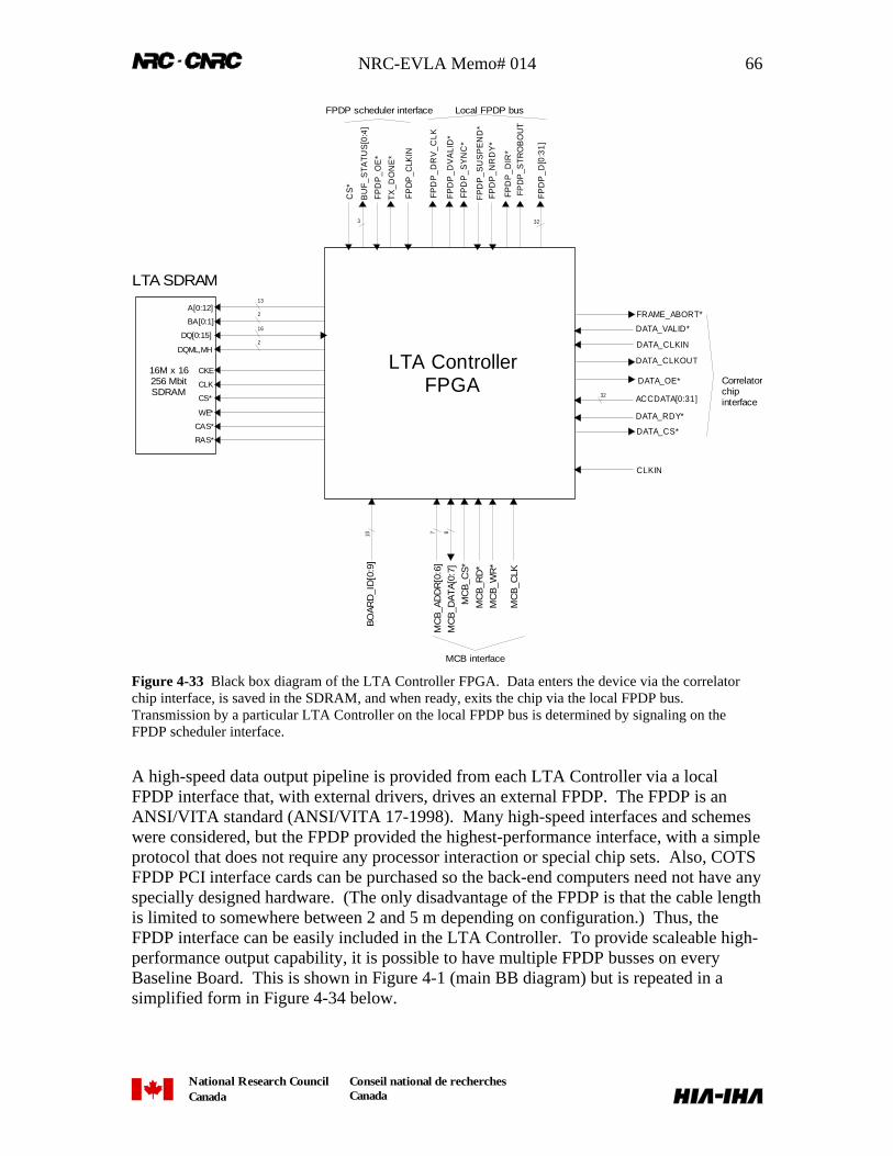
NRC-EVLA Memo# 014 66
National Research CouncilCanada
Conseil national de recherchesCanada
DATA_RDY*
ACCDATA[0:31]32
DATA_OE*
DATA_CLKIN
DATA_CLKOUT
DATA_VALID*
Correlatorchipinterface
16M x 16256 MbitSDRAM
LTA ControllerFPGA
A[0:12]
BA[0:1]
DQ[0:15]
DQML,MH2
13
2
16
CKE
CLK
CS*
WE*
CAS*
RAS*
CS
*
DATA_CS*
BU
F_S
TATU
S[0
:4]
3
FPD
P_C
LKIN
FPD
P_D
VA
LID
*
FPD
P_S
YN
C*
FPD
P_S
US
PE
ND
*
FPD
P_D
[0:3
1]
FPD
P_O
E*
FPDP scheduler interface
FPD
P_N
RD
Y*
32
FPD
P_D
RV
_CLK
MC
B_A
DD
R[0
:6]
MC
B_D
AT
A[0
:7]
MC
B_C
S*
MC
B_R
D*
MC
B_C
LK
7 8
MCB interface
MC
B_W
R*
LTA SDRAM
Local FPDP bus
TX_D
ON
E*
FPD
P_D
IR*
FPD
P_S
TRO
BO
UT
FRAME_ABORT*
CLKIN
BO
AR
D_I
D[0
:9]
10
Figure 4-33 Black box diagram of the LTA Controller FPGA. Data enters the device via the correlatorchip interface, is saved in the SDRAM, and when ready, exits the chip via the local FPDP bus.Transmission by a particular LTA Controller on the local FPDP bus is determined by signaling on theFPDP scheduler interface.
A high-speed data output pipeline is provided from each LTA Controller via a localFPDP interface that, with external drivers, drives an external FPDP. The FPDP is anANSI/VITA standard (ANSI/VITA 17-1998). Many high-speed interfaces and schemeswere considered, but the FPDP provided the highest-performance interface, with a simpleprotocol that does not require any processor interaction or special chip sets. Also, COTSFPDP PCI interface cards can be purchased so the back-end computers need not have anyspecially designed hardware. (The only disadvantage of the FPDP is that the cable lengthis limited to somewhere between 2 and 5 m depending on configuration.) Thus, theFPDP interface can be easily included in the LTA Controller. To provide scaleable high-performance output capability, it is possible to have multiple FPDP busses on everyBaseline Board. This is shown in Figure 4-1 (main BB diagram) but is repeated in asimplified form in Figure 4-34 below.
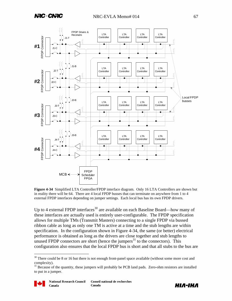
NRC-EVLA Memo# 014 67
National Research CouncilCanada
Conseil national de recherchesCanada
FP
DP
Con
nect
or
LTAController
LTAController
LTAController
LTAController
FP
DP
Con
nect
or
LTAController
LTAController
LTAController
LTAController
FP
DP
Con
nect
or
LTAController
LTAController
LTAController
LTAController
FPDPScheduler
FPGA
FPDP Drivers &Receivers
FP
DP
Con
nect
or
LTAController
LTAController
LTAController
LTAController
#1
#2
#3
#4
J1-T
J1-B
J2-T
J2-B
J3-T
J3-B
J4-T
J1-C
J2-C
J3-C
J4-C
MCB
Local FPDPbusses
Figure 4-34 Simplified LTA Controller/FPDP interface diagram. Only 16 LTA Controllers are shown butin reality there will be 64. There are 4 local FPDP busses that can terminate on anywhere from 1 to 4external FPDP interfaces depending on jumper settings. Each local bus has its own FPDP drivers.
Up to 4 external FPDP interfaces30 are available on each Baseline Board—how many ofthese interfaces are actually used is entirely user-configurable. The FPDP specificationallows for multiple TMs (Transmit Masters) connecting to a single FPDP via bussedribbon cable as long as only one TM is active at a time and the stub lengths are withinspecification. In the configuration shown in Figure 4-34, the same (or better) electricalperformance is obtained as long as the drivers are close together and stub lengths tounused FPDP connectors are short (hence the jumpers31 to the connectors). Thisconfiguration also ensures that the local FPDP bus is short and that all stubs to the bus are
30 There could be 8 or 16 but there is not enough front-panel space available (without some more cost andcomplexity).31 Because of the quantity, these jumpers will probably be PCB land pads. Zero-ohm resistors are installedto put in a jumper.
NRC-EVLA Memo# 014 68
National Research CouncilCanada
Conseil national de recherchesCanada
short. The relatively slow speed of the bus (25 nsec clock cycle) is also a good initialindication that the planned configuration should operate satisfactorily. The FPDPScheduler FPGA controls which LTA Controller is transmitting on the bus(ses) at a givenpoint in time (and controls which set of FPDP interface drivers are enabled for the givenconfiguration and enabled LTA Controller). It does this by simply querying each LTAController to see if it has data to transmit and what its ‘urgency’ is, and then enabling themost urgent LTA Controller for transmission.
Referring to Figure 4-33, the FPDP Scheduler interface signal functionality is as follows.
• CS* – Asserting this line enables the arbiter interface I/O drivers. Otherwiseoutput drivers are disabled, and the interface does not respond to arbiter signaling.
• BUF_STATUS[0:4] – These lines tell the FPDP Scheduler whether the LTAController has data to transmit and what the state of the LTA buffer memory is(i.e. how full it is). Bits 0-2 indicate relatively how full the LTA memory is. Ifthis is approaching the all 1’s state, then the LTA is getting ready to overflow. Bit3, if set, indicates that data is ready to be transmitted on the FPDP interface. Bit4, if set, indicates that ‘speed dump’ data is ready for transmission. This is datathat comes directly from the correlator chip, bypassing the LTA buffer (refer toFigure 4-5—DUMPTRIG format). BUF_STATUS bits can change at any timeand so they should be double-sampled by the arbiter.
• FPDP_OE* – Asserting this input causes the LTA Controller to enable its FPDPoutput drivers and start data transmission on the FPDP. The FPDP Schedulerasserts this signal when it wants the CS* enabled LTA Controller to transmit data.
• TX_DONE* – The LTA Controller asserts this line for one clock cycle when ithas finished an FPDP transmission.
• FPDP_CLKIN – This input clock is used to generate FPDP output clocks by theLTA Controller. This clock can be completely independent of the correlator chipclock.
A functional timing diagram for the LTA Controller’s FPDP scheduler interface andFPDP TM interface is shown in Figure 4-35. The FPDP TM timing is representative—allFPDP timing will be met once FPDP_OE* is asserted including FPDP_SUSPEND*,FPDP_NRDY*, and FPDP_DIR*. TX_DONE* is asserted for one clock edge only. IfFPDP_OE* is not removed within the next 4 clock edges, the next frame of data will betransmitted. If there is no data to be transmitted, TX_DONE* will be asserted again untilFPDP_OE* is negated or until the transmit buffer has data in it again. This way, multipleframes can be transmitted consecutively from one LTA Controller without having toquery its status and suffer waiting for 16 FPDP clock cycles32 every time.FPDP_DRV_CLK is used to drive the FPDP output drivers. FPDP_STROBOUT is used
32 The specification requires that the FPDP strobe be stable for 16 cycles before data is transmitted.
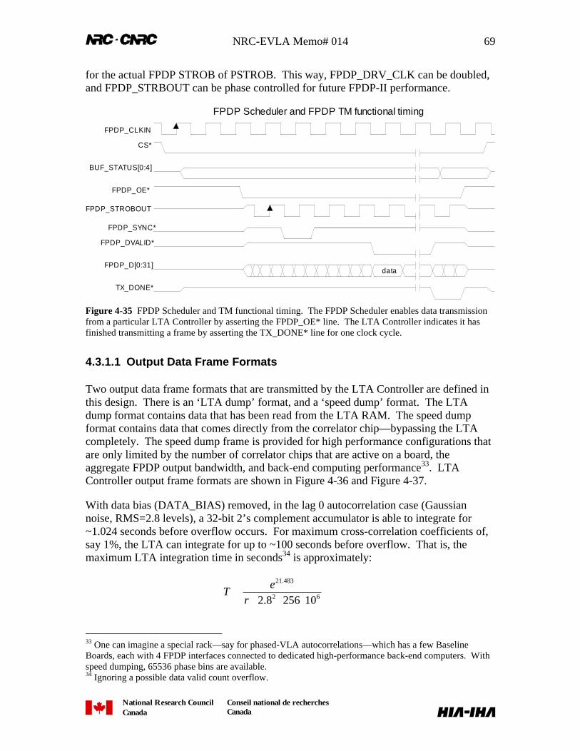
NRC-EVLA Memo# 014 69
National Research CouncilCanada
Conseil national de recherchesCanada
for the actual FPDP STROB of PSTROB. This way, FPDP_DRV_CLK can be doubled,and FPDP_STRBOUT can be phase controlled for future FPDP-II performance.
FPDP_CLKIN
CS*
BUF_STATUS[0:4]
FPDP_OE*
FPDP_STROBOUT
FPDP_SYNC*
FPDP_DVALID*
FPDP_D[0:31]
TX_DONE*
data
FPDP Scheduler and FPDP TM functional timing
Figure 4-35 FPDP Scheduler and TM functional timing. The FPDP Scheduler enables data transmissionfrom a particular LTA Controller by asserting the FPDP_OE* line. The LTA Controller indicates it hasfinished transmitting a frame by asserting the TX_DONE* line for one clock cycle.
4.3.1.1 Output Data Frame Formats
Two output data frame formats that are transmitted by the LTA Controller are defined inthis design. There is an ‘LTA dump’ format, and a ‘speed dump’ format. The LTAdump format contains data that has been read from the LTA RAM. The speed dumpformat contains data that comes directly from the correlator chip—bypassing the LTAcompletely. The speed dump frame is provided for high performance configurations thatare only limited by the number of correlator chips that are active on a board, theaggregate FPDP output bandwidth, and back-end computing performance33. LTAController output frame formats are shown in Figure 4-36 and Figure 4-37.
With data bias (DATA_BIAS) removed, in the lag 0 autocorrelation case (Gaussiannoise, RMS=2.8 levels), a 32-bit 2’s complement accumulator is able to integrate for~1.024 seconds before overflow occurs. For maximum cross-correlation coefficients of,say 1%, the LTA can integrate for up to ~100 seconds before overflow. That is, themaximum LTA integration time in seconds34 is approximately:
62
483.21
102568.2 ⋅⋅⋅≅
ρe
T
33 One can imagine a special rack—say for phased-VLA autocorrelations—which has a few BaselineBoards, each with 4 FPDP interfaces connected to dedicated high-performance back-end computers. Withspeed dumping, 65536 phase bins are available.34 Ignoring a possible data valid count overflow.
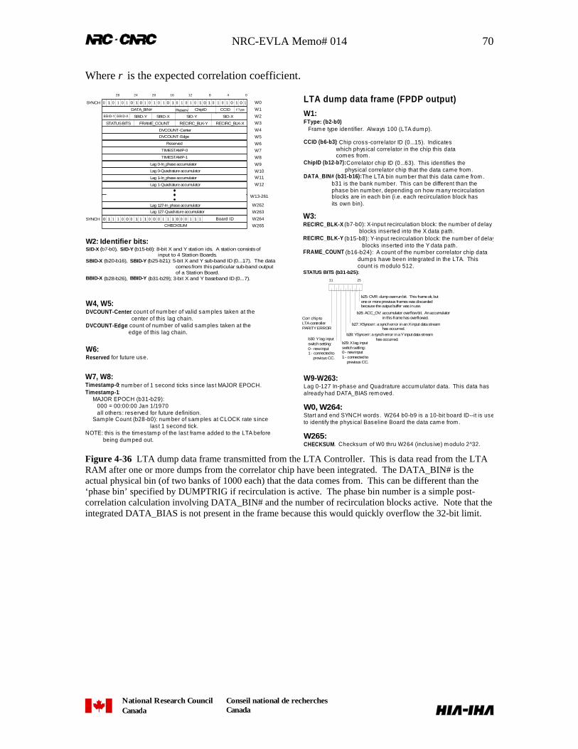
NRC-EVLA Memo# 014 70
National Research CouncilCanada
Conseil national de recherchesCanada
Where ρ is the expected correlation coefficient.0481216202428
1 0 1 0 1 0 1 0 1 0 1 0 1 0 1 0 1 0 1 0 1 0 1 0 1 0 1 0 1 0 10
SID-XSID-YSBID-XSBID-YBBID-XBBID-Y
FTypeCCID ChipID
RECIRC_BLK-XRECIRC_BLK-Y
DVCOUNT-Center
DVCOUNT-Edge
TIMESTAMP-0
TIMESTAMP-1
SYNCH
Lag 0-In_phase accumulator
Lag 0-Quadrature accumulator
Lag 1-In_phase accumulator
Lag 1-Quadrature accumulator
Lag 127-In_phase accumulator
Lag 127-Quadrature accumulator
0 1 1 1 0 0 0 0 0 0 0 0 01 1 1 1 1 1 1 1 1
CHECKSUM
W0
W1
W2
W3
W4
W5
W6
W7
W8
W9
W10W11
W12
W264
W265
W263
W262
W13-261
SYNCH Board ID
STATUS BITS FRAME_COUNT
DATA_BIN# Reserv
Reserved
2531
b25: OVR: dump overrun bit. This frame ok, butone or more previous frames was discardedbecause the output buffer was in use.
b27: XSyncerr: a synch error in an X input data stream has occurred.
b26: ACC_OV: accumulator overflow bit. An accumulator in this frame has overflowed.
b28: YSyncerr: a synch error in a Y input data stream has occurred.
b29: X lag inputswitch setting:0 - new input1 - connected to previous CC.
b30: Y lag inputswitch setting:0 - new input1 - connected to previous CC.
STATUS BITS (b31-b25):
Corr chip toLTA controllerPARITY ERROR
W1:FType: (b2-b0) Fram e type identifier. Always 100 (LTA dum p).
CCID (b6-b3): Chip cross-correlator ID (0...15). Indicates which phys ical correlator in the chip this data com es from.ChipID (b12-b7): Correlator chip ID (0...63). This identifies the phys ical correlator chip that the data came from.DATA_BIN# (b31-b16): The LTA bin number that this data cam e from . b31 is the bank number. This can be different than the phase bin num ber, depending on how many recirculation blocks are in each bin (i.e. each recirculation block has its own bin).
W2: Identifier bits:SID-X (b7-b0), SID-Y (b15-b8): 8-bit X and Y station ids. A station consists of input to 4 Station Boards.SBID-X (b20-b16), SBID-Y (b25-b21): 5-bit X and Y sub-band ID (0...17). The data comes from this particular sub-band output of a Station Board.BBID-X (b28-b26), BBID-Y (b31-b29); 3-bit X and Y baseband ID (0...7).
W3:RECIRC_BLK-X (b7-b0): X-input recirculation block: the number of delay blocks inserted into the X data path.RECIRC_BLK-Y (b15-b8): Y-input recirculation block: the num ber of delay blocks inserted into the Y data path.FRAME_COUNT (b16-b24): A count of the number correlator chip data dumps have been integrated in the LTA. This count is m odulo 512.
W4, W5:DVCOUNT-Center: count of num ber of valid samples taken at the center of this lag chain.DVCOUNT-Edge: count of number of valid sam ples taken at the edge of this lag chain.
W6:Reserved for future use.
W7, W8:Timestamp-0: num ber of 1 second ticks s ince las t MAJOR EPOCH.Timestamp-1: MAJOR EPOCH (b31-b29): 000 = 00:00:00 Jan 1/1970 all others : reserved for future definition. Sample Count (b28-b0): num ber of sam ples at CLOCK rate s ince las t 1 second tick.NOTE: this is the timestam p of the las t frame added to the LTA before being dum ped out.
W9-W263:Lag 0-127 In-phase and Quadrature accumulator data. This data hasalready had DATA_BIAS rem oved.
W0, W264:Start and end SYNCH words . W264 b0-b9 is a 10-bit board ID--it is useto identify the phys ical Baseline Board the data cam e from .
W265:CHECKSUM. Checksum of W0 thru W264 (inclus ive) m odulo 2^32.
LTA dump data frame (FPDP output)
Figure 4-36 LTA dump data frame transmitted from the LTA Controller. This is data read from the LTARAM after one or more dumps from the correlator chip have been integrated. The DATA_BIN# is theactual physical bin (of two banks of 1000 each) that the data comes from. This can be different than the‘phase bin’ specified by DUMPTRIG if recirculation is active. The phase bin number is a simple post-correlation calculation involving DATA_BIN# and the number of recirculation blocks active. Note that theintegrated DATA_BIAS is not present in the frame because this would quickly overflow the 32-bit limit.
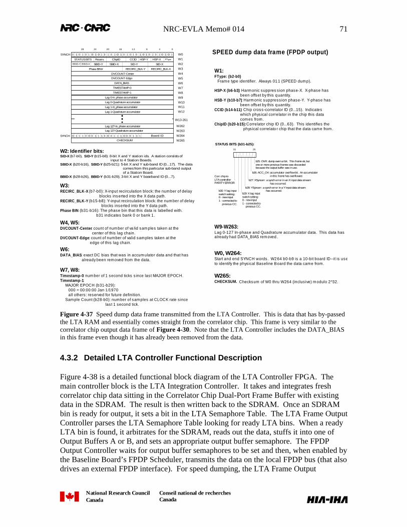
NRC-EVLA Memo# 014 71
National Research CouncilCanada
Conseil national de recherchesCanada
0481 216202428
1 0 1 0 1 0 1 0 1 0 1 0 1 0 1 0 1 0 1 0 1 0 1 0 1 0 1 0 1 0 10
SID-XSID-YSBID-XSBID-YBBID-XBBID-Y
FTypeHSP-XHSP-YCCIDSTATUS BITS ChipID Reserv.
RECIRC_BLK-XRECIRC_BLK-YPhase BIN#
DVCOUNT-Center
DVCOUNT-Edge
DATA_BIAS
TIMESTAMP-0
TIMESTAMP-1
SYNCH
Lag 0-In_phase accumulator
Lag 0-Quadrature accumulator
Lag 1-In_phase accumulator
Lag 1-Quadrature accumulator
Lag 127-In_phase accumulator
Lag 127-Quadrature accumulator
0 1 1 1 0 0 0 0 0 0 0 0 01 1 1 1 1 1 1 1 1
CHECKSUM
W0
W1
W2
W3
W4
W5
W6
W7
W8
W9
W10W11
W12
W264
W265
W263
W262
W13-261
SYNCH Board ID
2531
b25: OVR: dump overrun bit. This frame ok, butone or more previous frames was discardedbecause the output buffer was in use.
b27: XSyncerr: a synch error in an X input data stream has occurred.
b26: ACC_OV: accumulator overflow bit. An accumulator in this frame has overflowed.
b28: YSyncerr: a synch error in a Y input data stream has occurred.
b29: X lag inputswitch setting:0 - new input1 - connected to previous CC.
b30: Y lag inputswitch setting:0 - new input1 - connected to previous CC.
STATUS BITS (b31-b25):
Corr chip toLTA controllerPARITY ERROR
W1:FType: (b2-b0) Frame type identifier. Always 01 1 (SPEED dump).
HSP-X (b6-b3): Harmonic suppres s ion phase-X. X-phase has been offset by this q uantity.HSB-Y (b10-b7): Harmonic suppress ion phase-Y. Y-phase has been offset by this q uantity.CCID (b14-b11): Chip cross-correlator ID (0...15). Indicates which phys ical correlator in the chip this data comes from.ChipID (b20-b15): Correlator chip ID (0...63). This identifies the phys ical correlato r chip that the data came from.
W2: Identifier bits:SID-X (b7-b0), SID-Y (b15-b8): 8-bit X and Y station ids. A station consists of input to 4 Station Boards.SBID-X (b20-b16), SBID-Y (b25-b21): 5-bit X and Y sub-band ID (0...17). The data comes from this particular sub-band output of a Station Board.BBID-X (b28-b26), BBID-Y (b31-b29); 3-bit X and Y baseband ID (0...7).
W3:RECIRC_BLK-X (b7-b0): X-input recirculation block: the number of delay blocks inserted into the X data path.RECIRC_BLK-Y (b15-b8): Y-input recirculation block: the num ber of delay blocks inserted into the Y data path.Phase BIN (b31-b16): The phase bin that this data is labelled with. b31 indicates bank 0 or bank 1.
W4, W5:DVCOUNT-Center: count of number of va lid sam ples taken at the center of this lag chain.DVCOUNT-Edge: count of number of valid samples taken at the edge of this lag chain.
W6:DATA_BIAS: exact DC bias that was in accum ulator data and that has already been removed from the data.
W7, W8:Timestamp-0: num ber of 1 second ticks s ince las t MAJOR EPOCH.Timestamp-1: MAJOR EPOCH (b31-b29): 000 = 00:00:00 Jan 1/1970 all others : reserved for future definition. Sample Count (b28-b0): number of samples at CLOCK rate s ince las t 1 second tick.
W9-W263:Lag 0-127 In-phase and Quadrature accumulator data. This data hasalready had DATA_BIAS removed .
W0, W264:Start and end SYNCH words. W2 64 b0-b9 is a 10-bit board ID--it is useto identify the phys ical Baseline Board the data came from.
W265:CHECKSUM. Checksum of W0 thru W264 (inclus ive) modulo 2^32.
SPEED dump data frame (FPDP output)
Figure 4-37 Speed dump data frame transmitted from the LTA Controller. This is data that has by-passedthe LTA RAM and essentially comes straight from the correlator chip. This frame is very similar to thecorrelator chip output data frame of Figure 4-30. Note that the LTA Controller includes the DATA_BIASin this frame even though it has already been removed from the data.
4.3.2 Detailed LTA Controller Functional Description
Figure 4-38 is a detailed functional block diagram of the LTA Controller FPGA. Themain controller block is the LTA Integration Controller. It takes and integrates freshcorrelator chip data sitting in the Correlator Chip Dual-Port Frame Buffer with existingdata in the SDRAM. The result is then written back to the SDRAM. Once an SDRAMbin is ready for output, it sets a bit in the LTA Semaphore Table. The LTA Frame OutputController parses the LTA Semaphore Table looking for ready LTA bins. When a readyLTA bin is found, it arbitrates for the SDRAM, reads out the data, stuffs it into one ofOutput Buffers A or B, and sets an appropriate output buffer semaphore. The FPDPOutput Controller waits for output buffer semaphores to be set and then, when enabled bythe Baseline Board’s FPDP Scheduler, transmits the data on the local FPDP bus (that alsodrives an external FPDP interface). For speed dumping, the LTA Frame Output
NRC-EVLA Memo# 014 72
National Research CouncilCanada
Conseil national de recherchesCanada
Controller gets notified directly by the Correlator Chip Readout Controller that data isready. This prompts the LTA Frame Output Controller to stuff the data directly into oneof the output buffers—bypassing the LTA SDRAM. In the figure, bold lines are dataflows and thin lines are control lines.
The LTA Integration Controller is designed so that if all phase bins (that are active) for aparticular CCID are full it discards data from the correlator chip for that CCID until all ofthose phase bins are empty. This way it is possible to burst dump 2000 phase bins, notlose any data, and then suffer some dead time while the buffers are being emptied. Also,correlator chip data is discarded if the phase bin it is destined for contains data ready forreadout.
Previously, it was mentioned that a detailed paper design of the LTA Controller was doneso that an accurate logic device estimate could be made. The top-level schematicdiagram from this paper design is shown in Figure 4-39. This design, if a 128 MHzcorrelator chip readout clock is used with a 100 Mbytes/sec FPDP, should meet thefollowing performance specifications:
• If all correlator chip data is dumped with reasonably long phase-bin integrationtimes so the SDRAM is not accessed very often to output the data, the phase binscan be as narrow as ~180 µsec.
• If only one ‘lag cell’ (known by the LTA Controller as a ‘CCID’) is dumped, thephase bins can be as narrow as ~12 µsec (with a reasonably long phase-binintegration time).
• If the LTA just integrates one frame and the entire correlator chip is dumped, theintegration time is ~320 µsec (assuming no FPDP bottleneck). That is, the real-time sustained dump rate is 320 µsec.
• The entire Baseline Board can be dumped every ~10.5 msec (each dump is, ofcourse, several correlator chip dumps and LTA integrations).
• If speed dumping is used with a dedicated FPDP (i.e. only one correlator chipactive per FPDP and with a ~200 Mbytes/sec FPDP), one CCID frame can beoutput every 5 µsec. With this mode, up to 65,536 pulsar phase bins can bedefined. This is the extreme performance case.
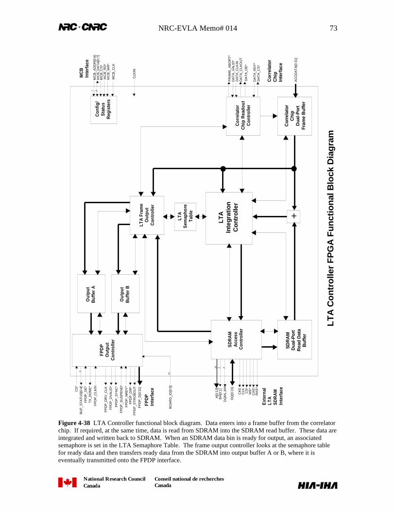
NRC-EVLA Memo# 014 73
National Research CouncilCanada
Conseil national de recherchesCanada
LTA
Inte
grat
ion
Con
trol
ler
Cor
rela
tor
Chi
p R
eado
utC
ontr
olle
r
Cor
rela
tor
Chi
pD
ual-P
ort
Fram
e B
uffe
r
SD
RA
MA
cces
sC
ontr
olle
r
SD
RA
MD
ual-P
ort
Rea
d D
ata
Buf
fer
+
LTA
Fra
me
Out
put
Con
trol
ler
LTA
Sem
apho
reTa
ble
Out
put
Buf
fer
A
Out
put
Buf
fer
B
FPD
PO
utpu
tC
ontr
olle
r
Con
fig/
Sta
tus
Reg
iste
rs
MC
BIn
terf
ace
Cor
rela
tor
Chi
pIn
terf
ace
FPD
PIn
terf
ace
Ext
erna
lLT
AS
DR
AM
Inte
rfac
e
LT
A C
on
tro
ller
FP
GA
Fu
nct
ion
al B
lock
Dia
gra
m
DA
TA
_RD
Y*
AC
CD
AT
A[0
:31]
DA
TA
_OE
*
DA
TA
_CLK
IND
AT
A_C
LKO
UT
DA
TA
_VA
LID
*
DA
TA
_CS
*
FR
AM
E_A
BO
RT
*
CLK
IN
MC
B_A
DD
R[0
:6]
MC
B_D
AT
A[0
:7]
MC
B_C
S*
MC
B_R
D*
MC
B_C
LK
7 8
MC
B_W
R*
A[0
:12]
BA
[0:1
]
DQ
[0:1
5]
DQ
ML,
MH
213 2
CK
EC
LK CS
*W
E*
CA
S*
RA
S*
CS
*B
UF
_ST
AT
US
[0:4
]3
FP
DP
_CLK
IN
FP
DP
_DV
ALI
D*
FP
DP
_SY
NC
*F
PD
P_S
US
PE
ND
*
FP
DP
_D[0
:31]
FP
DP
_OE
*
FP
DP
_NR
DY
*
FP
DP
_DR
V_C
LK
TX
_DO
NE
*
FP
DP
_DIR
*F
PD
P_S
TR
OB
OU
T
BO
AR
D_I
D[0
:9]
10
Figure 4-38 LTA Controller functional block diagram. Data enters into a frame buffer from the correlatorchip. If required, at the same time, data is read from SDRAM into the SDRAM read buffer. These data areintegrated and written back to SDRAM. When an SDRAM data bin is ready for output, an associatedsemaphore is set in the LTA Semaphore Table. The frame output controller looks at the semaphore tablefor ready data and then transfers ready data from the SDRAM into output buffer A or B, where it iseventually transmitted onto the FPDP interface.
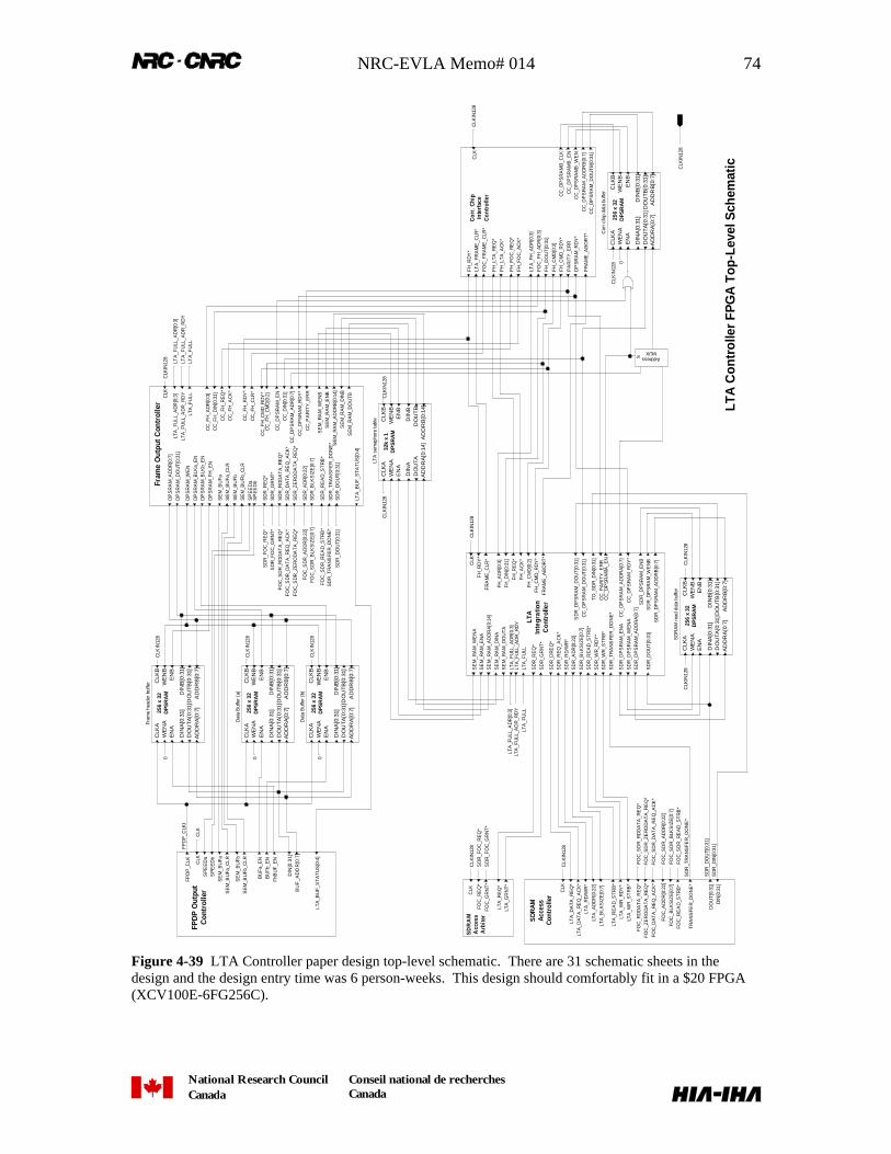
NRC-EVLA Memo# 014 74
National Research CouncilCanada
Conseil national de recherchesCanada
SD
RA
M r
ead
data
buf
fer
256
x 32
DPS
RA
M
AD
DR
A[0
:7]
DIN
A[0
:31]
WE
NA
CLK
A
EN
A
DO
UTA
[0:3
1]A
DD
RB
[0:7
]
DIN
B[0
:31]
WE
NB
CLK
B
EN
B
DO
UT
B[0
:31]
Fram
e O
utpu
t C
ontr
olle
r
SE
M_R
AM
_WE
NB
SE
M_R
AM
_EN
BS
EM
_RA
M_A
DD
RB
[0:1
4]S
EM
_RA
M_D
INB
SE
M_R
AM
_DO
UTBC
LK
SD
R_R
DD
AT
A_R
EQ
*S
DR
_DA
TA_R
EQ
_AC
K*
SD
R_A
DR
[0:2
2]
SD
R_D
OU
T[0:
31]
DP
SR
AM
_DO
UT
[0:3
1]D
PS
RA
M_A
DD
R[0
:7]
DP
SR
AM
_WE
ND
PS
RA
M_B
LKa_
EN
DP
SR
AM
_BLK
b_E
N
CC
_FH
_RD
Y*
CC
_FH
_CLR
*
CC
_FH
_AD
R[0
:3]
CC
_FH
_DIN
[0:3
1]C
C_F
H_R
EQ
*C
C_F
H_A
CK
*
DP
SR
AM
_FH
_EN
SE
M_B
UFa
SE
M_B
UFa
_CLR
SE
M_B
UFb
SE
M_B
UFb
_CLR
LTA
_BU
F_S
TATU
S[0
:4]
CC
_DIN
[0:3
1]
LTA
_FU
LL_A
DR
[0:3
]
LTA
_FU
LL
CC
_DP
SR
AM
_EN
CC
_FH
_CM
D_R
DY
*C
C_F
H_C
MD
[0:2
]
CC
_DP
SR
AM
_AD
R[0
:7]
SD
R_B
LKS
IZE
[0:7
]
SD
R_R
EA
D_S
TRB
*
SD
R_T
RA
NS
FER
_DO
NE
*
LTA
_FU
LL_A
DR
_RD
Y
CC
_DP
SR
AM
_RD
Y*
SD
R_R
EQ
*S
DR
_GR
NT*
SD
R_Z
ER
OD
ATA
_RE
Q*
SP
EE
Da
SP
EE
Db
CC
_PA
RIT
Y_E
RR
FPD
P O
utpu
tC
ontr
olle
r BU
F_A
DD
R[0
:7]
DIN
[0:3
1]
SE
M_B
UFa
SE
M_B
UFa
_CLR
SE
M_B
UFb
SE
M_B
UFb
_CLR
FPD
P_C
LK
BU
Fa_E
NB
UFb
_EN
FhB
UF_
EN
LTA
_BU
F_S
TAT
US
[0:4
]
SP
EE
Da
SP
EE
Db
CLK
SD
RA
MA
cces
sC
ontr
olle
r
LTA
_AD
DR
[0:2
2]
DIN
[0:3
1]D
OU
T[0:
31]
CLK
LTA
_DA
TA_R
EQ
*
LTA
_RD
/WR
*
LTA
_RE
AD
_STR
B*
LTA
_WR
_RD
Y*
LTA
_WR
_ST
RB
*
LTA
_DA
TA_R
EQ
_AC
K*
LTA
_BLK
SIZ
E[0
:7]
FOC
_AD
DR
[0:2
2]
FOC
_RD
DA
TA_R
EQ
*
FOC
_RE
AD
_STR
B*
FOC
_DA
TA_R
EQ
_AC
K*
FOC
_BLK
SIZ
E[0
:7]
TRA
NS
FER
_DO
NE
*
FOC
_ZE
RO
DA
TA_R
EQ
*
LTA
Inte
grat
ion
Con
trol
ler
FH_A
DR
[0:3
]FH
_DIN
[0:3
1]
FH_R
DY
*F
RA
ME
_CLR
*
SD
R_R
EQ
*S
DR
_GR
NT
*
CLK
SD
R_D
RE
Q*
SD
R_R
EQ
_AC
K*
SD
R_R
D/W
R*
SD
R_A
DR
[0:2
2]
SD
R_R
EA
D_S
TRB
*
SD
R_D
PS
RA
M_E
NA
SD
R_D
PS
RA
M_W
EN
AS
DR
_DP
SR
AM
_AD
DR
A[0
:7]
SD
R_D
PS
RA
M_E
NB
SD
R_D
PS
RA
M_W
EN
BS
DR
_DP
SR
AM
_AD
DR
B[0
:7]
CC
_DP
SR
AM
A_E
N
CC
_DP
SR
AM
_AD
DR
A[0
:7]
SD
R_D
PS
RA
M_D
OU
T[0:
31]
CC
_DP
SR
AM
_DO
UT
[0:3
1]
TO_S
DR
_DIN
[0:3
1]
SD
R_T
RA
NS
FER
_DO
NE
*
FH_R
EQ
*FH
_AC
K*
FH_C
MD
[0:2
]FH
_CM
D_R
DY
*
CC
_DP
SR
AM
_RD
Y*
SE
M_R
AM
_WE
NA
SE
M_R
AM
_EN
AS
EM
_RA
M_A
DD
RA
[0:1
4]S
EM
_RA
M_D
INA
SE
M_R
AM
_DO
UTA
FRA
ME
_AB
OR
T*
LTA
_FU
LL_A
DR
[0:3
]
LTA
_FU
LL
CC
_PA
RIT
Y_E
RR
SD
R_B
LKS
IZE
[0:7
]
SD
R_W
R_R
DY
*S
DR
_WR
_STR
B*
SD
R_D
OU
T[0
:31]
LTA
_FU
LL_A
DR
_RD
Y
SD
RA
MA
cces
sA
rbite
r
LTA
_RE
Q*
LTA
_GR
NT*
FOC
_RE
Q*
FOC
_GR
NT
*
CLK
Dat
a B
uffe
r (a)
256
x 32
DPS
RA
M
AD
DR
A[0
:7]
DIN
A[0
:31]
WE
NA
CLK
A
EN
A
DO
UTA
[0:3
1]A
DD
RB
[0:7
]
DIN
B[0
:31]
WE
NB
CLK
B
EN
B
DO
UTB
[0:3
1]
Dat
a B
uffe
r (b)
256
x 32
DPS
RA
M
AD
DR
A[0
:7]
DIN
A[0
:31]
WE
NA
CLK
A
EN
A
DO
UTA
[0:3
1]A
DD
RB
[0:7
]
DIN
B[0
:31]
WE
NB
CLK
B
EN
B
DO
UTB
[0:3
1]
Cor
r. C
hip
Inte
rfac
eC
ontr
olle
r CC
_DP
SR
AM
B_E
NC
C_D
PS
RA
MB
_WE
NC
C_D
PS
RA
M_A
DD
RB
[0:7
]
LTA
_FH
_AD
R[0
:3]
FH_L
TA_R
EQ
*FH
_LTA
_AC
K*
FH_D
OU
T[0:
31]
FH_F
OC
_RE
Q*
FH_F
OC
_AC
K*
FH_C
MD
[0:2
]FH
_CM
D_R
DY
*
DP
SR
AM
_RD
Y*
FH_R
DY
*LT
A_F
RA
ME
_CLR
*C
LK
CC
_DP
SR
AM
_DO
UTB
[0:3
1]
FOC
_FR
AM
E_C
LR*
FRA
ME
_AB
OR
T*
CC
_DP
SR
AM
B_C
LK
FOC
_FH
_AD
R[0
:3] Cor
r chi
p da
ta b
uffe
r
256
x 32
DP
SR
AM
AD
DR
A[0
:7]
DIN
A[0
:31]
WE
NA
CLK
A
EN
A
DO
UT
A[0
:31]
AD
DR
B[0
:7]
DIN
B[0
:31]
WE
NB
CLK
B
EN
B
DO
UTB
[0:3
1]
32k
x 1
DP
SR
AM
AD
DR
A[0
:14]
DIN
A
WE
NA
CLK
A
EN
A
DO
UTA
AD
DR
B[0
:14]
DIN
B
WE
NB
CLK
B
EN
B
DO
UT
B
LTA
sem
apho
re ta
ble
256
x 32
DPS
RA
M
AD
DR
A[0
:7]
DIN
A[0
:31]
WE
NA
CLK
A
EN
A
DO
UTA
[0:3
1]A
DD
RB
[0:7
]
DIN
B[0
:31]
WE
NB
CLK
B
EN
B
DO
UTB
[0:3
1]
Fram
e he
ader
buf
fer
CLK
IN12
8
CLK
IN12
8
CLK
IN12
8
CLK
IN12
8
CLK
IN12
8
CLK
IN12
8
CLK
IN12
8
CLK
IN12
8
CLK
IN12
8C
LKIN
128
SD
R_F
OC
_RE
Q*
SD
R_F
OC
_GR
NT*
SD
R_D
OU
T[0:
31]
SD
R_D
OU
T[0:
31]
CLK
IN12
80 0 0
FPD
P_C
LKI
CLK
IN12
8
CLK
IN12
8
CLK
IN12
8
LTA
Con
trol
ler
FPG
A T
op-L
evel
Sch
emat
ic
PA
RIT
Y_E
RR
LTA
_FU
LL_A
DR
[0:3
]
LTA
_FU
LL
LTA
_FU
LL_A
DR
[0:3
]
LTA
_FU
LL
0
AddressMUX
S
SD
R_D
IN[0
:31]
SD
R_T
RA
NS
FER
_DO
NE
*
FOC
_SD
R_R
DD
ATA
_RE
Q*
FOC
_SD
R_D
ATA
_RE
Q_A
CK
*
FOC
_SD
R_A
DD
R[0
:22]
FOC
_SD
R_B
LKS
IZE
[0:7
]FO
C_S
DR
_RE
AD
_ST
RB
*
FO
C_S
DR
_RD
DA
TA
_RE
Q*
FOC
_SD
R_D
ATA
_RE
Q_A
CK
*
FOC
_SD
R_A
DD
R[0
:22]
FOC
_SD
R_B
LKS
IZE
[0:7
]
FOC
_SD
R_R
EA
D_S
TRB
*S
DR
_TR
AN
SFE
R_D
ON
E*
LTA
_FU
LL_A
DR
_RD
Y
LTA
_FU
LL_A
DR
_RD
Y
SD
R_F
OC
_RE
Q*
SD
R_F
OC
_GR
NT*
FOC
_SD
R_Z
ER
OD
ATA
_RE
Q*
FOC
_SD
R_Z
ER
OD
AT
A_R
EQ
*
CLK
Figure 4-39 LTA Controller paper design top-level schematic. There are 31 schematic sheets in thedesign and the design entry time was 6 person-weeks. This design should comfortably fit in a $20 FPGA(XCV100E-6FG256C).
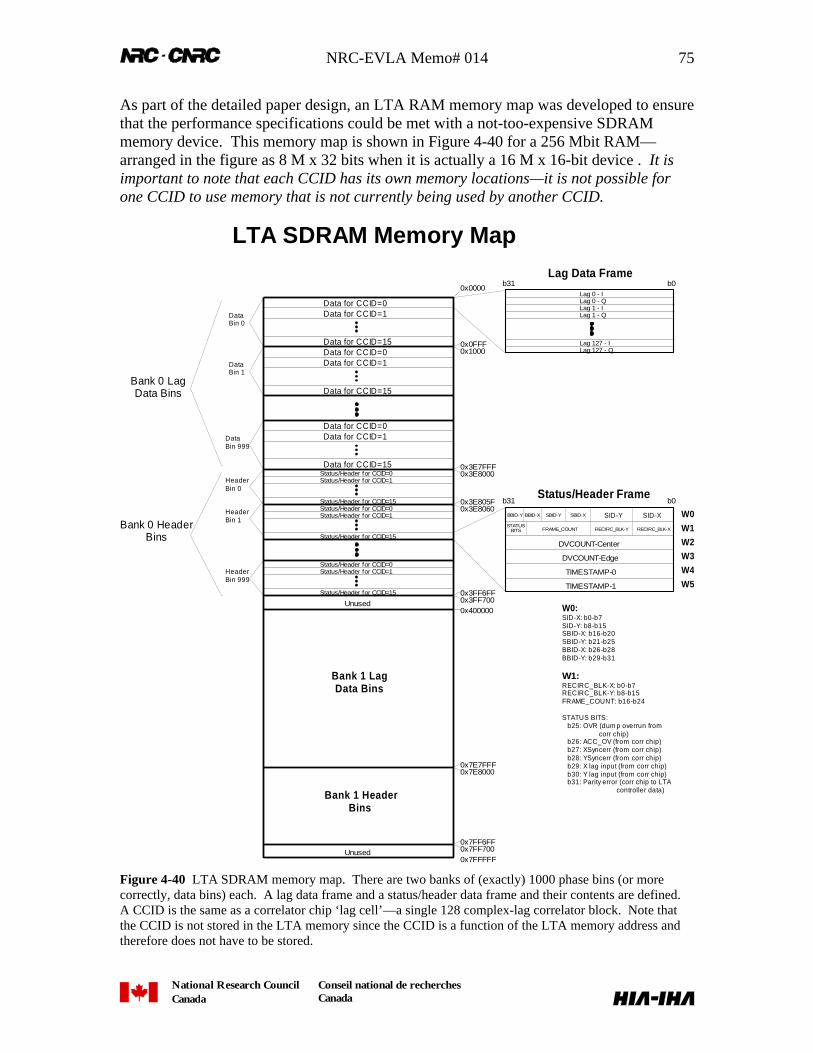
NRC-EVLA Memo# 014 75
National Research CouncilCanada
Conseil national de recherchesCanada
As part of the detailed paper design, an LTA RAM memory map was developed to ensurethat the performance specifications could be met with a not-too-expensive SDRAMmemory device. This memory map is shown in Figure 4-40 for a 256 Mbit RAM—arranged in the figure as 8 M x 32 bits when it is actually a 16 M x 16-bit device . It isimportant to note that each CCID has its own memory locations—it is not possible forone CCID to use memory that is not currently being used by another CCID.
Data for CCID=0Data for CCID=1
Data for CCID=15
Lag 0 - ILag 0 - QLag 1 - ILag 1 - Q
Lag 127 - ILag 127 - Q
DataBin 0
Data for CCID=0Data for CCID=1
Data for CCID=15
Data for CCID=0Data for CCID=1
Data for CCID=15 0x3E7FFF
0x0FFF
Status/Header for CCID=0Status/Header for CCID=1
Status/Header for CCID=15
DataBin 1
DataBin 999
0x0000
0x1000
0x3E8000HeaderBin 0
Status/Header for CCID=0Status/Header for CCID=1
Status/Header for CCID=15
Status/Header for CCID=0Status/Header for CCID=1
Status/Header for CCID=15
HeaderBin 1
HeaderBin 999
0x3E80600x3E805F
0x3FF6FF0x3FF700Unused
SID-XSID-YSBID-XSBID-YBBID-XBBID-Y
RECIRC_BLK-XRECIRC_BLK-YSTATUS
BITS FRAME_COUNT
DVCOUNT-Center
DVCOUNT-Edge
TIMESTAMP-0
TIMESTAMP-1
Lag Data Frame
Status/Header Frame
0x400000
Bank 0 LagData Bins
Bank 0 HeaderBins
W0:SID-X: b0-b7SID-Y: b8-b15SBID-X: b16-b20SBID-Y: b21-b25BBID-X: b26-b28BBID-Y: b29-b31
W1:RECIRC_BLK-X: b0-b7RECIRC_BLK-Y: b8-b15FRAME_COUNT: b16-b24
STATUS BITS: b25: OVR (dum p overrun from corr chip) b26: ACC_OV (from corr chip) b27: XSyncerr (from corr chip) b28: YSyncerr (from corr chip) b29: X lag input (from corr chip) b30: Y lag input (from corr chip) b31: Parity error (corr chip to LTA controller data)
0x7E7FFF0x7E8000
Bank 1 LagData Bins
0x7FF7000x7FF6FF
0x7FFFFF
Bank 1 HeaderBins
Unused
W0W1W2W3W4W5
b0b31
LTA SDRAM Memory Map
b0b31
Figure 4-40 LTA SDRAM memory map. There are two banks of (exactly) 1000 phase bins (or morecorrectly, data bins) each. A lag data frame and a status/header data frame and their contents are defined.A CCID is the same as a correlator chip ‘lag cell’—a single 128 complex-lag correlator block. Note thatthe CCID is not stored in the LTA memory since the CCID is a function of the LTA memory address andtherefore does not have to be stored.
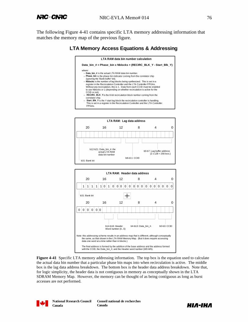
NRC-EVLA Memo# 014 76
National Research CouncilCanada
Conseil national de recherchesCanada
The following Figure 4-41 contains specific LTA memory addressing information thatmatches the memory map of the previous figure.
LTA Memory Access Equations & Addressing
Data_bin_# = Phase_bin x Nblocks + (RECIRC_BLK_Y - Start_Blk_Y)
where: -- Data_bin_# is the actual LTA RAM data bin number. -- Phase_bin is the phase bin indicator coming from the correlator chip (ignoring the 'Bank buffer' bit). -- Nblocks is the number of lag blocks being synthesized. This is set in a register in the Recirculation Controller and the LTA Controller FPGAs. Without any recirculation, this is 1. Data from each CCID must be enabled to use Nblocks or 1 (depending on whether recirculation is active for the CCID or not). -- RECIRC_BLK_Y is the 8-bit recirculation block number coming from the correlator chip. -- Start_Blk_Y is the Y start lag block the recirculation controller is handling. This is set in a register in the Recirculation Controller and the LTA Controller FPGAs.
LTA RAM data bin number calculation
048121620
b0-b7: Lag buffer address (2 x 128 = 256 locs.)
b8-b11: CCID
b12-b21: Data_bin_#: the actual LTA RAM data bin number
b31: Bank bit
LTA RAM: Lag data address
048121620
1 1 1 1 1 0 1 0 0 0 0 0 0 0 0 0 0 0 0 0 0 0
b31: Bank bit
048121620
b0-b3: CCIDb4-b13: Data_bin_#.b14-b16: HeaderWord number (0...5)
000000
Note: this addressing scheme results in an address map that is different, although conceptually the same, as that shown in the LTA RAM Memory Map. (But it does require accessing data one word at a time rather than in blocks.)
The final address is formed by the addition of the base address and the address formed with the CCID, the Data_bin_#, and the Header word number (W0-W5).
LTA RAM: Header data address
Figure 4-41 Specific LTA memory addressing information. The top box is the equation used to calculatethe actual data bin number that a particular phase bin maps into when recirculation is active. The middlebox is the lag data address breakdown. The bottom box is the header data address breakdown. Note that,for logic simplicity, the header data is not contiguous in memory as conceptually shown in the LTASDRAM Memory Map. However, the memory can be thought of as being contiguous as long as burstaccesses are not performed.
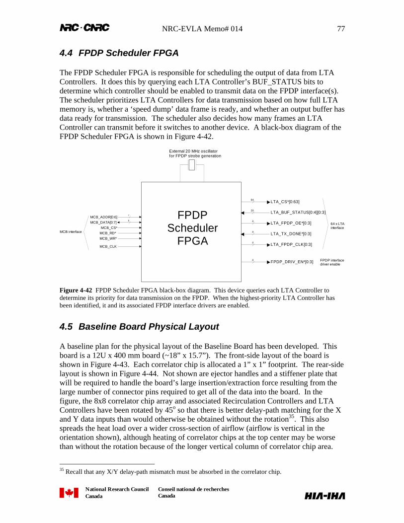
NRC-EVLA Memo# 014 77
National Research CouncilCanada
Conseil national de recherchesCanada
4.4 FPDP Scheduler FPGA
The FPDP Scheduler FPGA is responsible for scheduling the output of data from LTAControllers. It does this by querying each LTA Controller’s BUF_STATUS bits todetermine which controller should be enabled to transmit data on the FPDP interface(s).The scheduler prioritizes LTA Controllers for data transmission based on how full LTAmemory is, whether a ‘speed dump’ data frame is ready, and whether an output buffer hasdata ready for transmission. The scheduler also decides how many frames an LTAController can transmit before it switches to another device. A black-box diagram of theFPDP Scheduler FPGA is shown in Figure 4-42.
FPDPScheduler
FPGA
LTA_CS*[0:63]
LTA_BUF_STATUS[0:4][0:3]
LTA_FPDP_OE*[0:3]
LTA_TX_DONE*[0:3]
LTA_FPDP_CLK[0:3]
64
20
4
4
4
MCB_ADDR[0:6]MCB_DATA[0:7]
MCB_CS*MCB_RD*
MCB_CLK
7
8
MCB interface
MCB_WR*
64 x LTAinterface
FPDP_DRIV_EN*[0:3]4 FPDP interfacedriver enable
External 20 MHz oscillatorfor FPDP strobe generation
Figure 4-42 FPDP Scheduler FPGA black-box diagram. This device queries each LTA Controller todetermine its priority for data transmission on the FPDP. When the highest-priority LTA Controller hasbeen identified, it and its associated FPDP interface drivers are enabled.
4.5 Baseline Board Physical Layout
A baseline plan for the physical layout of the Baseline Board has been developed. Thisboard is a 12U x 400 mm board (~18” x 15.7”). The front-side layout of the board isshown in Figure 4-43. Each correlator chip is allocated a 1” x 1” footprint. The rear-sidelayout is shown in Figure 4-44. Not shown are ejector handles and a stiffener plate thatwill be required to handle the board’s large insertion/extraction force resulting from thelarge number of connector pins required to get all of the data into the board. In thefigure, the 8x8 correlator chip array and associated Recirculation Controllers and LTAControllers have been rotated by 45o so that there is better delay-path matching for the Xand Y data inputs than would otherwise be obtained without the rotation35. This alsospreads the heat load over a wider cross-section of airflow (airflow is vertical in theorientation shown), although heating of correlator chips at the top center may be worsethan without the rotation because of the longer vertical column of correlator chip area.
35 Recall that any X/Y delay-path mismatch must be absorbed in the correlator chip.
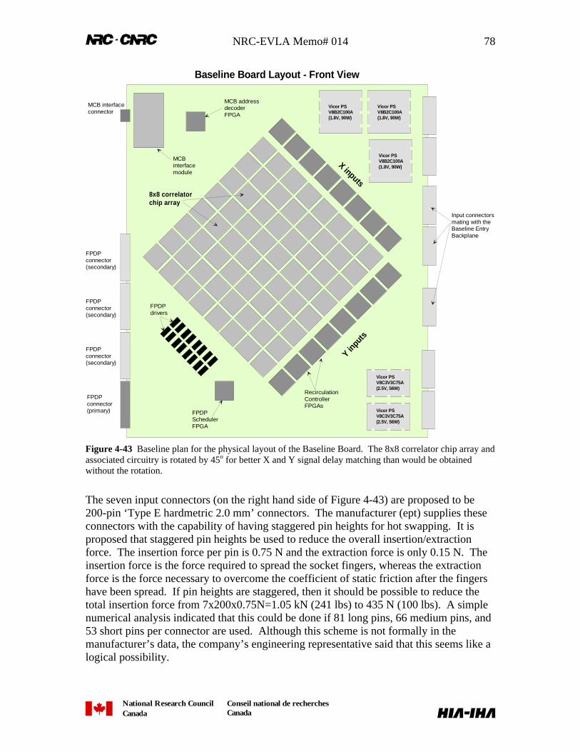
NRC-EVLA Memo# 014 78
National Research CouncilCanada
Conseil national de recherchesCanada
Vicor PSV8B2C100A(1.8V, 90W)
Vicor PSV8B2C100A(1.8V, 90W)
Vicor PSV8B2C100A(1.8V, 90W)
Vicor PSV8C3V3C75A(2.5V, 56W)
Vicor PSV8C3V3C75A(2.5V, 56W)
MCB interfaceconnector
MCBinterfacemodule
8x8 correlatorchip array
FPDPdrivers
FPDPSchedulerFPGA
RecirculationControllerFPGAs
FPDPconnector(primary)
FPDPconnector(secondary)
FPDPconnector(secondary)
FPDPconnector(secondary)
Input connectorsmating with theBaseline EntryBackplane
X inputs
Y inpu
ts
MCB addressdecoderFPGA
Baseline Board Layout - Front View
Figure 4-43 Baseline plan for the physical layout of the Baseline Board. The 8x8 correlator chip array andassociated circuitry is rotated by 45o for better X and Y signal delay matching than would be obtainedwithout the rotation.
The seven input connectors (on the right hand side of Figure 4-43) are proposed to be200-pin ‘Type E hardmetric 2.0 mm’ connectors. The manufacturer (ept) supplies theseconnectors with the capability of having staggered pin heights for hot swapping. It isproposed that staggered pin heights be used to reduce the overall insertion/extractionforce. The insertion force per pin is 0.75 N and the extraction force is only 0.15 N. Theinsertion force is the force required to spread the socket fingers, whereas the extractionforce is the force necessary to overcome the coefficient of static friction after the fingershave been spread. If pin heights are staggered, then it should be possible to reduce thetotal insertion force from 7x200x0.75N=1.05 kN (241 lbs) to 435 N (100 lbs). A simplenumerical analysis indicated that this could be done if 81 long pins, 66 medium pins, and53 short pins per connector are used. Although this scheme is not formally in themanufacturer’s data, the company’s engineering representative said that this seems like alogical possibility.
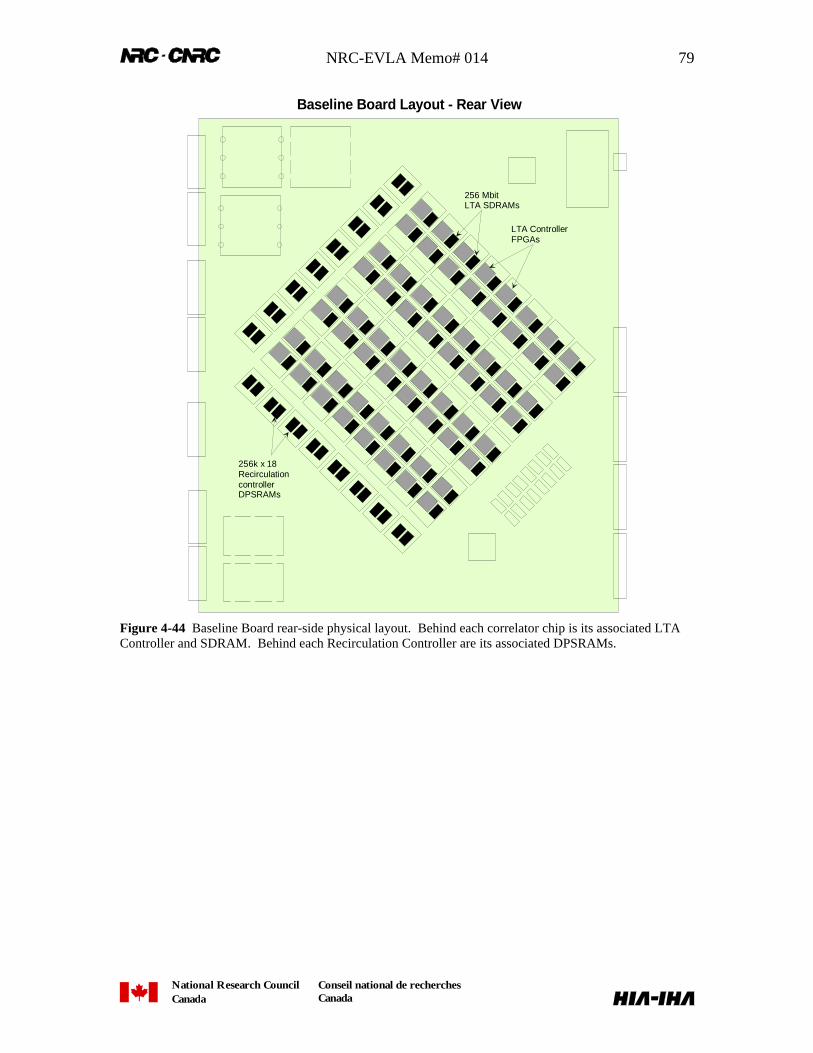
NRC-EVLA Memo# 014 79
National Research CouncilCanada
Conseil national de recherchesCanada
Baseline Board Layout - Rear View
LTA ControllerFPGAs
256 MbitLTA SDRAMs
256k x 18RecirculationcontrollerDPSRAMs
Figure 4-44 Baseline Board rear-side physical layout. Behind each correlator chip is its associated LTAController and SDRAM. Behind each Recirculation Controller are its associated DPSRAMs.
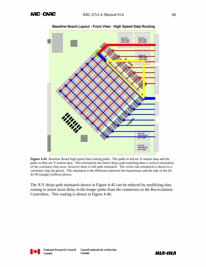
NRC-EVLA Memo# 014 80
National Research CouncilCanada
Conseil national de recherchesCanada
Vicor PSV8B2C100A(1.8V, 90W)
Vicor PSV8B2C100A(1.8V, 90W)
Vicor PSV8B2C100A(1.8V, 90W)
Vicor PSV8C3V3C75A(2.5V, 56W)
Vicor PSV8C3V3C75A(2.5V, 56W)
X inputs
Y input
s
Baseline Board Layout - Front View - High Speed Data Routing
Figure 4-45 Baseline Board high speed data routing paths. The paths in red are X-station data and thepaths in blue are Y-station data. This orientation has better delay-path matching than a vertical orientationof the correlator chip array, however there is still path mismatch. The worst case mismatch is shown to acorrelator chip (in green). The mismatch is the difference between the hypotenuse and the side of the 45-45-90 triangle (yellow) shown.
The X/Y delay-path mismatch shown in Figure 4-45 can be reduced by modifying datarouting to insert more delay in the longer paths from the connectors to the RecirculationControllers. This routing is shown in Figure 4-46.
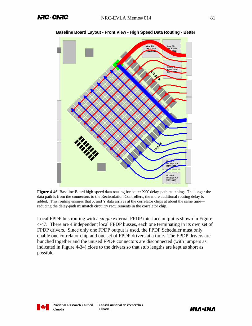
NRC-EVLA Memo# 014 81
National Research CouncilCanada
Conseil national de recherchesCanada
Vicor PSV8B2C100A(1.8V, 90W)
Vicor PSV8B2C100A(1.8V, 90W)
Vicor PSV8B2C100A(1.8V, 90W)
Vicor PSV8C3V3C75A(2.5V, 56W)
Vicor PSV8C3V3C75A(2.5V, 56W)
X inputs
Y inpu
ts
Baseline Board Layout - Front View - High Speed Data Routing - Better
Figure 4-46 Baseline Board high-speed data routing for better X/Y delay-path matching. The longer thedata path is from the connectors to the Recirculation Controllers, the more additional routing delay isadded. This routing ensures that X and Y data arrives at the correlator chips at about the same time—reducing the delay-path mismatch circuitry requirements in the correlator chip.
Local FPDP bus routing with a single external FPDP interface output is shown in Figure4-47. There are 4 independent local FPDP busses, each one terminating in its own set ofFPDP drivers. Since only one FPDP output is used, the FPDP Scheduler must onlyenable one correlator chip and one set of FPDP drivers at a time. The FPDP drivers arebunched together and the unused FPDP connectors are disconnected (with jumpers asindicated in Figure 4-34) close to the drivers so that stub lengths are kept as short aspossible.
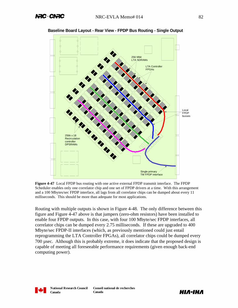
NRC-EVLA Memo# 014 82
National Research CouncilCanada
Conseil national de recherchesCanada
Baseline Board Layout - Rear View - FPDP Bus Routing - Single Output
LTA ControllerFPGAs
256 MbitLTA SDRAMs
256k x 18RecirculationcontrollerDPSRAMs
LocalFPDPbusses
Single primaryTM FPDP interface
Figure 4-47 Local FPDP bus routing with one active external FPDP transmit interface. The FPDPScheduler enables only one correlator chip and one set of FPDP drivers at a time. With this arrangementand a 100 Mbytes/sec FPDP interface, all lags from all correlator chips can be dumped about every 11milliseconds. This should be more than adequate for most applications.
Routing with multiple outputs is shown in Figure 4-48. The only difference between thisfigure and Figure 4-47 above is that jumpers (zero-ohm resistors) have been installed toenable four FPDP outputs. In this case, with four 100 Mbyte/sec FPDP interfaces, allcorrelator chips can be dumped every 2.75 milliseconds. If these are upgraded to 400Mbyte/sec FPDP-II interfaces (which, as previously mentioned could just entailreprogramming the LTA Controller FPGAs), all correlator chips could be dumped every700 µsec. Although this is probably extreme, it does indicate that the proposed design iscapable of meeting all foreseeable performance requirements (given enough back-endcomputing power).
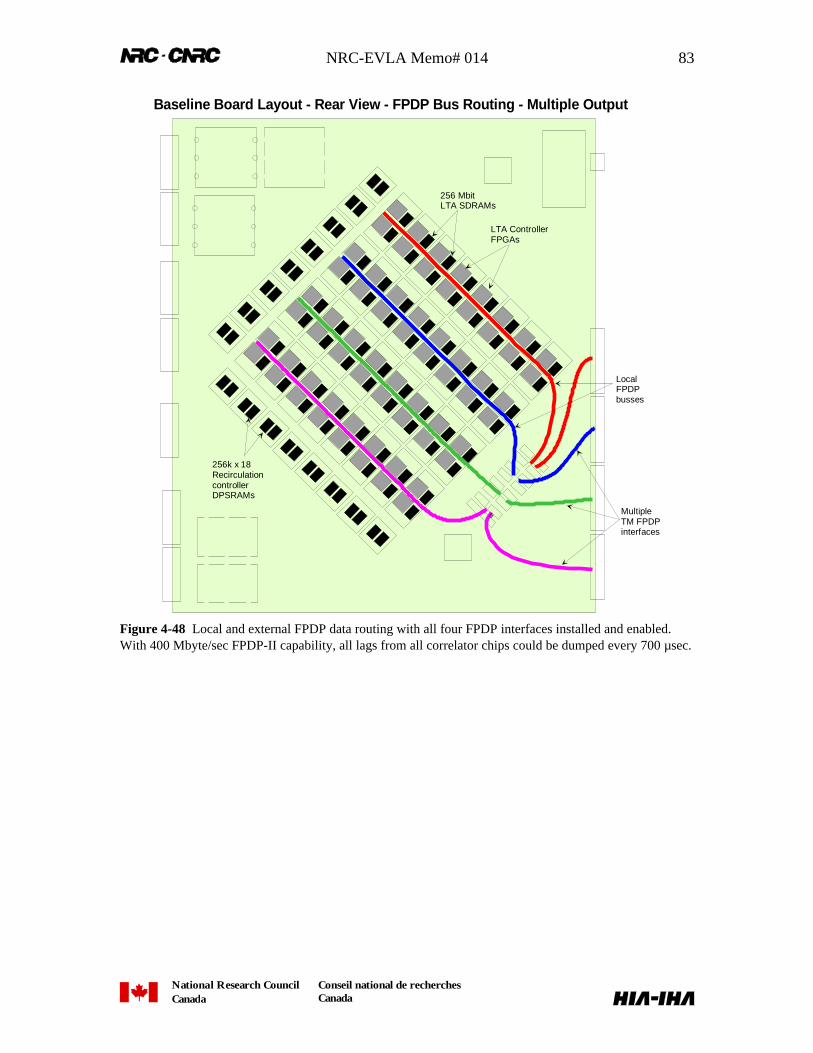
NRC-EVLA Memo# 014 83
National Research CouncilCanada
Conseil national de recherchesCanada
Baseline Board Layout - Rear View - FPDP Bus Routing - Multiple Output
LTA ControllerFPGAs
256 MbitLTA SDRAMs
256k x 18RecirculationcontrollerDPSRAMs
=
LocalFPDPbusses
MultipleTM FPDPinterfaces
Figure 4-48 Local and external FPDP data routing with all four FPDP interfaces installed and enabled.With 400 Mbyte/sec FPDP-II capability, all lags from all correlator chips could be dumped every 700 µsec.
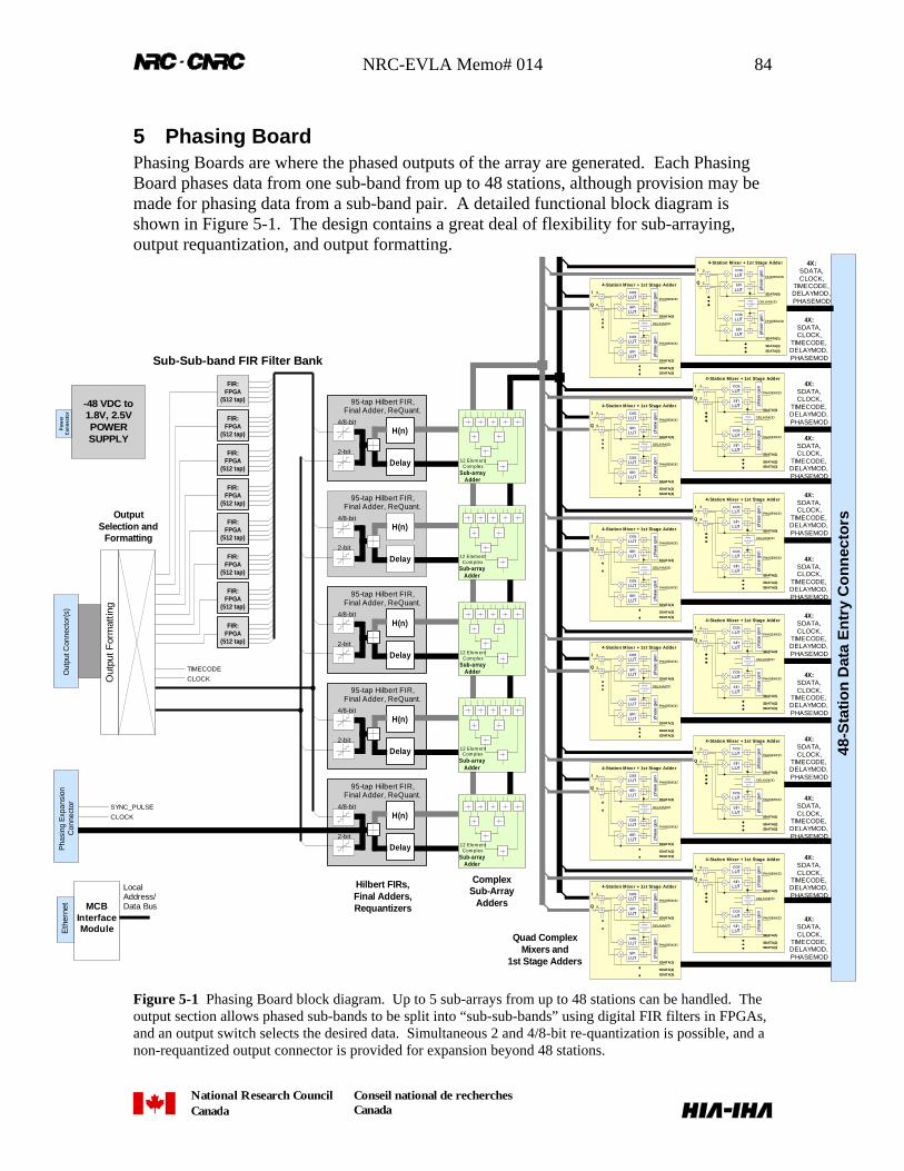
NRC-EVLA Memo# 014 84
National Research CouncilCanada
Conseil national de recherchesCanada
5 Phasing BoardPhasing Boards are where the phased outputs of the array are generated. Each PhasingBoard phases data from one sub-band from up to 48 stations, although provision may bemade for phasing data from a sub-band pair. A detailed functional block diagram isshown in Figure 5-1. The design contains a great deal of flexibility for sub-arraying,output requantization, and output formatting.
cosLUT
sinLUT ph
ase
gen
delay -to- phas e
LUT
cosLUT
sinLUT ph
ase
gen
SDATA(0)
PHASEMOD
DELAYMOD
PHASEMOD
SDATA(1)
SDATA(2)SDATA(3)
9
9
I
Q
4-Station Mixe r + 1st Stage Adder
cosLUT
sinLUT ph
ase
gen
delay -to- phas e
LUT
cosLUT
sinLUT ph
ase
gen
SDATA(0)
PHASEMOD
DELAYMOD
PHASEMOD
SDATA(1)
SDATA(2)SDATA(3)
9
9
I
Q
4-Station Mixe r + 1st Stage Adder
cosLUT
sinLUT ph
ase
gen
delay -to- phas e
LUT
cosLUT
sinLUT ph
ase
gen
SDATA(0)
PHASEMOD
DELAYMOD
PHASEMOD
SDATA(1)
SDATA(2)SDATA(3)
9
9
I
Q
4-Station Mixe r + 1st Stage Adder
cosLUT
sinLUT ph
ase
gen
delay -to- phas e
LUT
cosLUT
sinLUT ph
ase
gen
SDATA(0)
PHASEMOD
DELAYMOD
PHASEMOD
SDATA(1)
SDATA(2)SDATA(3)
9
9
I
Q
4-Station Mixe r + 1st Stage Adder
cosLUT
sinLUT ph
ase
gen
delay -to-phas e
LUT
cosLUT
sinLUT ph
ase
gen
SDATA(0)
PHASEMOD
DELAYMOD
PHASEMOD
SDATA(1)
SDATA(2)SDATA(3)
9
9
I
Q
4-Station Mixer + 1st Stage Adder
cosLUT
sinLUT ph
ase
gen
delay -to-phas e
LUT
cosLUT
sinLUT ph
ase
gen
SDATA(0)
PHASEMOD
DELAYMOD
PHASEMOD
SDATA(1)
SDATA(2)SDATA(3)
9
9
I
Q
4-Station Mixer + 1st Stage Adder
cosLUT
sinLUT ph
ase
gen
delay -to-phas e
LUT
cosLUT
sinLUT ph
ase
gen
SDATA(0)
PHASEMOD
DELAYMOD
PHASEMOD
SDATA(1)
SDATA(2)SDATA(3)
9
9
I
Q
4-Station Mixer + 1st Stage Adder
cosLUT
sinLUT ph
ase
gen
delay -to-phas e
LUT
cosLUT
sinLUT ph
ase
gen
SDATA(0)
PHASEMOD
DELAYMOD
PHASEMOD
SDATA(1)
SDATA(2)SDATA(3)
9
9
I
Q
4-Station Mixer + 1st Stage Adder
cosLUT
sinLUT ph
ase
gen
delay -to-phas e
LUT
cosLUT
sinLUT ph
ase
gen
SDATA(0)
PHASEMOD
DELAYMOD
PHASEMOD
SDATA(1)
SDATA(2)SDATA(3)
9
9
I
Q
4-Station Mixer + 1st Stage Adder
48-S
tatio
n D
ata
En
try
Co
nn
ecto
rs
4X:SDATA,CLOCK,
TIMECODE,DELAYMOD,PHASEMOD
4X:SDATA,CLOCK,
TIMECODE,DELAYMOD,PHASEMOD
4X:SDATA,CLOCK,
TIMECODE,DELAYMOD,PHASEMOD
4X:SDATA,CLOCK,
TIMECODE,DELAYMOD,PHASEMOD
4X:SDATA,CLOCK,
TIMECODE,DELAYMOD,PHASEMOD
4X:SDATA,CLOCK,
TIMECODE,DELAYMOD,PHASEMOD
4X:SDATA,CLOCK,
TIMECODE,DELAYMOD,PHASEMOD
4X:SDATA,CLOCK,
TIMECODE,DELAYMOD,PHASEMOD
4X:SDATA,CLOCK,
TIMECODE,DELAYMOD,PHASEMOD
4X:SDATA,CLOCK,
TIMECODE,DELAYMOD,PHASEMOD
95-tap Hilbert FIR,Final Adder, ReQuant.
H(n)
Delay
4/8-bit
2-bit12 Elem ent
Com plexSub-array
Adder
12 ElementCom plex
Sub-arrayAdder
12 Elem entCom plex
Sub-arrayAdder
12 Elem entCom plex
Sub-arrayAdder
12 Elem entCom plex
Sub-arrayAdder
Out
put C
onne
ctor
(s)
Sub-Sub-band FIR Filter Bank
FIR:FPGA
(512 tap)-48 VDC to1.8V, 2.5VPOWERSUPPLY
Pow
erC
onne
cto
r
ComplexSub-Array
Adders
Hilbert FIRs,Final Adders,Requantizers
Quad ComplexMixers and
1st Stage Adders
95-tap Hilbert FIR,Final Adder, ReQuant.
H(n)
Delay
4/8-bit
2-bit
95-tap Hilbert FIR,Final Adder, ReQuant.
H(n)
Delay
4/8-bit
2-bit
95-tap Hilbert FIR,Final Adder, ReQuant.
H(n)
Delay
4/8-bit
2-bit
95-tap Hilbert FIR,Final Adder, ReQuant.
H(n)
Delay
4/8-bit
2-bit
FIR:FPGA
(512 tap)
FIR:FPGA
(512 tap)
FIR:FPGA
(512 tap)
FIR:FPGA
(512 tap)
FIR:FPGA
(512 tap)
FIR:FPGA
(512 tap)
FIR:FPGA
(512 tap)
Out
put F
orm
attin
g
TIMECODECLOCK
Pha
sing
Exp
ansi
onC
onne
ctor SYNC_PULSE
CLOCK
OutputSelection and
Formatting
MCBInterfaceModule
LocalAddress/Data Bus
Eth
erne
t
cosLUT
sinLUT ph
ase
gen
delay -to-phas e
LUT
cosLUT
sinLUT ph
ase
gen
SDATA(0)
PHASEMOD
DELAYMOD
PHASEMOD
SDATA(1)
SDATA(2)SDATA(3)
9
9
I
Q
4-Station Mixer + 1st Stage Adde r
cosLUT
sinLUT ph
ase
gen
delay -to- phas e
LUT
cosLUT
sinLUT ph
ase
gen
SDATA(0)
PHASEMOD
DELAYMOD
PHASEMOD
SDATA(1)
SDATA(2)SDATA(3)
9
9
I
Q
4-Station Mixe r + 1st Stage Adder
4X:SDATA,CLOCK,
TIMECODE,DELAYMOD,PHASEMOD
4X:SDATA,CLOCK,
TIMECODE,DELAYMOD,PHASEMOD
cosLUT
sinLUT ph
ase
gen
delay -to- phas e
LUT
cosLUT
sinLUT ph
ase
gen
SDATA(0)
PHASEMOD
DELAYMOD
PHASEMOD
SDATA(1)
SDATA(2)SDATA(3)
9
9
I
Q
4-Station Mixe r + 1st Stage Adder
Figure 5-1 Phasing Board block diagram. Up to 5 sub-arrays from up to 48 stations can be handled. Theoutput section allows phased sub-bands to be split into “sub-sub-bands” using digital FIR filters in FPGAs,and an output switch selects the desired data. Simultaneous 2 and 4/8-bit re-quantization is possible, and anon-requantized output connector is provided for expansion beyond 48 stations.
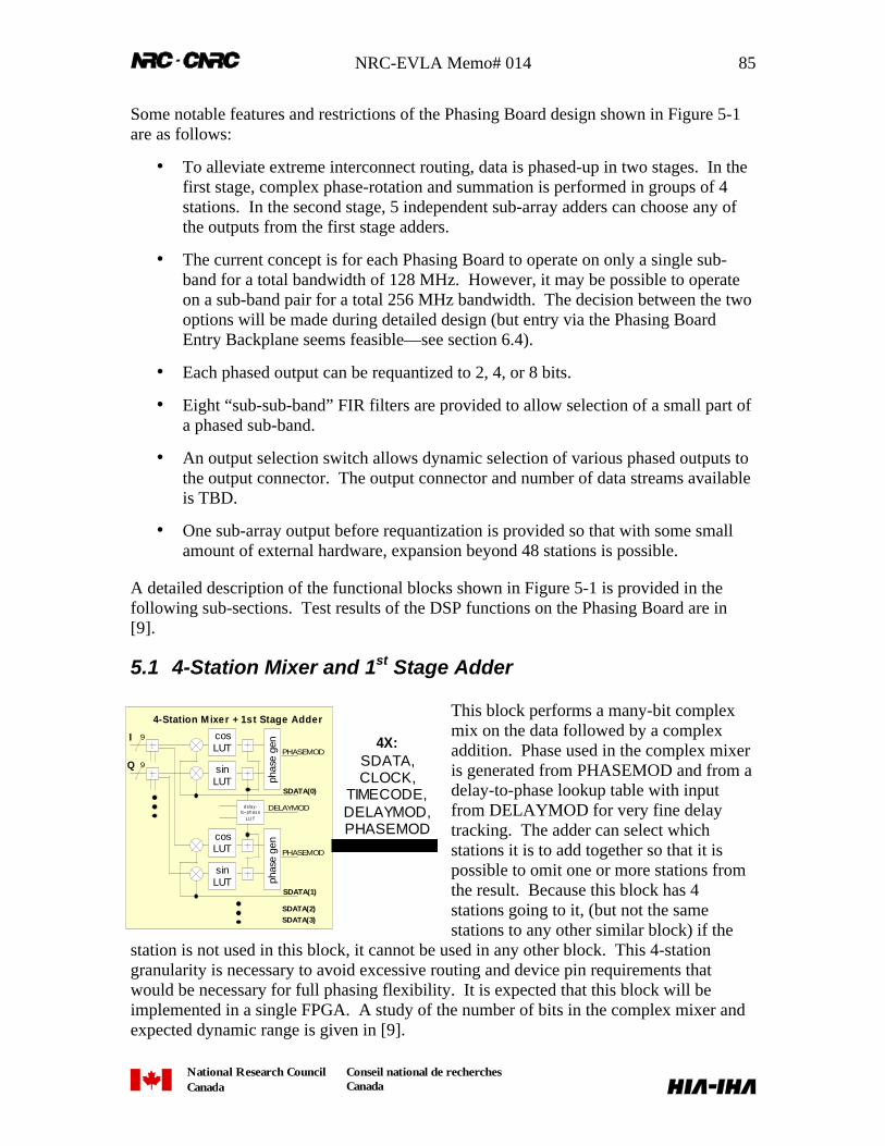
NRC-EVLA Memo# 014 85
National Research CouncilCanada
Conseil national de recherchesCanada
Some notable features and restrictions of the Phasing Board design shown in Figure 5-1are as follows:
• To alleviate extreme interconnect routing, data is phased-up in two stages. In thefirst stage, complex phase-rotation and summation is performed in groups of 4stations. In the second stage, 5 independent sub-array adders can choose any ofthe outputs from the first stage adders.
• The current concept is for each Phasing Board to operate on only a single sub-band for a total bandwidth of 128 MHz. However, it may be possible to operateon a sub-band pair for a total 256 MHz bandwidth. The decision between the twooptions will be made during detailed design (but entry via the Phasing BoardEntry Backplane seems feasible—see section 6.4).
• Each phased output can be requantized to 2, 4, or 8 bits.
• Eight “sub-sub-band” FIR filters are provided to allow selection of a small part ofa phased sub-band.
• An output selection switch allows dynamic selection of various phased outputs tothe output connector. The output connector and number of data streams availableis TBD.
• One sub-array output before requantization is provided so that with some smallamount of external hardware, expansion beyond 48 stations is possible.
A detailed description of the functional blocks shown in Figure 5-1 is provided in thefollowing sub-sections. Test results of the DSP functions on the Phasing Board are in[9].
5.1 4-Station Mixer and 1st Stage Adder
This block performs a many-bit complexmix on the data followed by a complexaddition. Phase used in the complex mixeris generated from PHASEMOD and from adelay-to-phase lookup table with inputfrom DELAYMOD for very fine delaytracking. The adder can select whichstations it is to add together so that it ispossible to omit one or more stations fromthe result. Because this block has 4stations going to it, (but not the samestations to any other similar block) if the
station is not used in this block, it cannot be used in any other block. This 4-stationgranularity is necessary to avoid excessive routing and device pin requirements thatwould be necessary for full phasing flexibility. It is expected that this block will beimplemented in a single FPGA. A study of the number of bits in the complex mixer andexpected dynamic range is given in [9].
cosLUT
sinLUT ph
ase
gen
d elay -to-phas e
LU T
cosLUT
sinLUT ph
ase
gen
SDATA(0)
PHASEMOD
DELAYMOD
PHASEMOD
SDATA(1)
SDATA(2)SDATA(3)
9
9
I
Q
4-Station Mixer + 1st Stage Adder
4X:SDATA,CLOCK,
TIMECODE,DELAYMOD,PHASEMOD
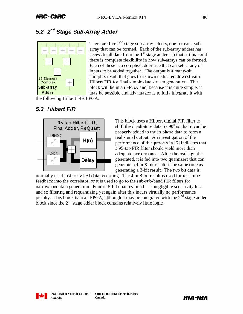
NRC-EVLA Memo# 014 86
National Research CouncilCanada
Conseil national de recherchesCanada
5.2 2nd Stage Sub-Array Adder
There are five 2nd stage sub-array adders, one for each sub-array that can be formed. Each of the sub-array adders hasaccess to all data from the 1st stage adders so that at this pointthere is complete flexibility in how sub-arrays can be formed.Each of these is a complex adder tree that can select any ofinputs to be added together. The output is a many-bitcomplex result that goes to its own dedicated downstreamHilbert FIR for final simple data stream generation. Thisblock will be in an FPGA and, because it is quite simple, itmay be possible and advantageous to fully integrate it with
the following Hilbert FIR FPGA.
5.3 Hilbert FIR
This block uses a Hilbert digital FIR filter toshift the quadrature data by 90o so that it can beproperly added to the in-phase data to form areal signal output. An investigation of theperformance of this process in [9] indicates thata 95-tap FIR filter should yield more thanadequate performance. After the real signal isgenerated, it is fed into two quantizers that cangenerate a 4 or 8-bit result at the same time asgenerating a 2-bit result. The two bit data is
normally used just for VLBI data recording. The 4 or 8-bit result is used for real-timefeedback into the correlator, or it is used to go to the sub-sub-band FIR filters fornarrowband data generation. Four or 8-bit quantization has a negligible sensitivity lossand so filtering and requantizing yet again after this incurs virtually no performancepenalty. This block is in an FPGA, although it may be integrated with the 2nd stage adderblock since the 2nd stage adder block contains relatively little logic.
12 Elem entCom plex
Sub-arrayAdder
95-tap Hilbert FIR,Final Adder, ReQuant.
H(n)
Delay
4/8-bit
2-bit
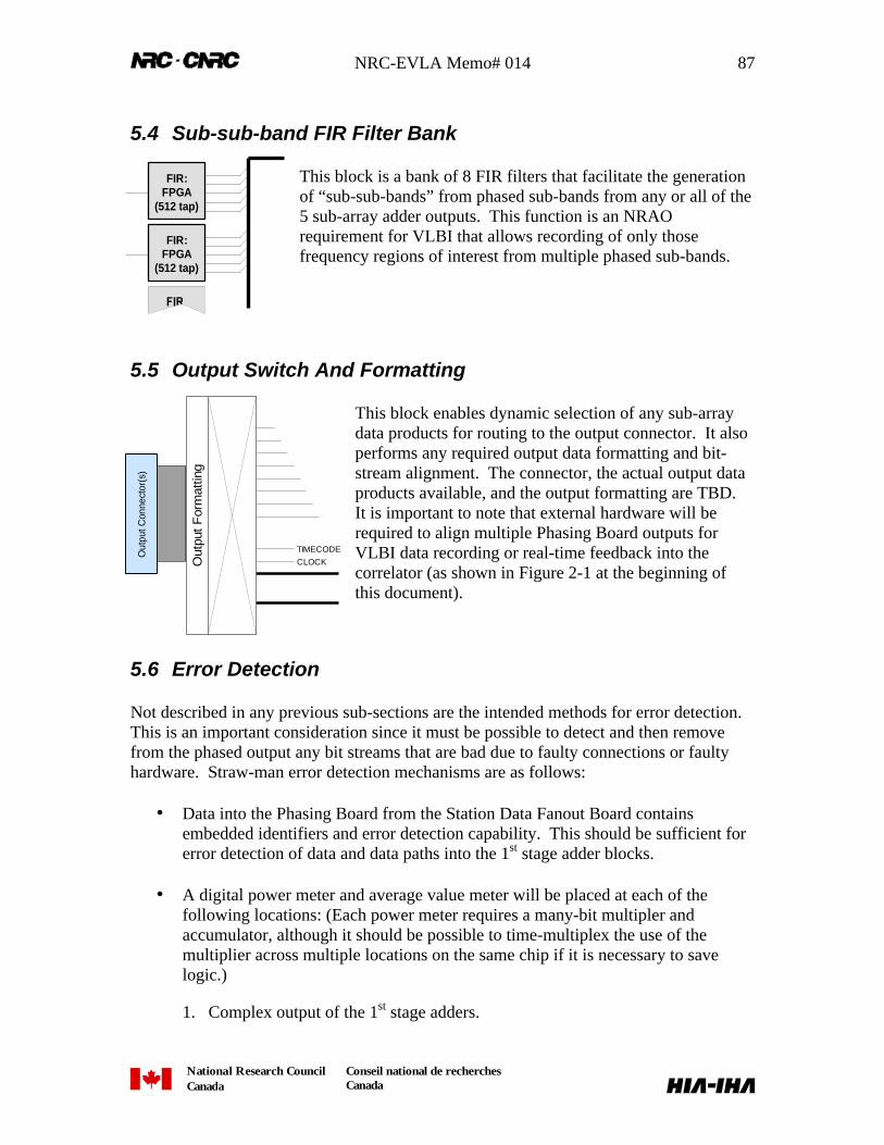
NRC-EVLA Memo# 014 87
National Research CouncilCanada
Conseil national de recherchesCanada
5.4 Sub-sub-band FIR Filter Bank
This block is a bank of 8 FIR filters that facilitate the generationof “sub-sub-bands” from phased sub-bands from any or all of the5 sub-array adder outputs. This function is an NRAOrequirement for VLBI that allows recording of only thosefrequency regions of interest from multiple phased sub-bands.
5.5 Output Switch And Formatting
This block enables dynamic selection of any sub-arraydata products for routing to the output connector. It alsoperforms any required output data formatting and bit-stream alignment. The connector, the actual output dataproducts available, and the output formatting are TBD.It is important to note that external hardware will berequired to align multiple Phasing Board outputs forVLBI data recording or real-time feedback into thecorrelator (as shown in Figure 2-1 at the beginning ofthis document).
5.6 Error Detection
Not described in any previous sub-sections are the intended methods for error detection.This is an important consideration since it must be possible to detect and then removefrom the phased output any bit streams that are bad due to faulty connections or faultyhardware. Straw-man error detection mechanisms are as follows:
• Data into the Phasing Board from the Station Data Fanout Board containsembedded identifiers and error detection capability. This should be sufficient forerror detection of data and data paths into the 1st stage adder blocks.
• A digital power meter and average value meter will be placed at each of thefollowing locations: (Each power meter requires a many-bit multipler andaccumulator, although it should be possible to time-multiplex the use of themultiplier across multiple locations on the same chip if it is necessary to savelogic.)
1. Complex output of the 1st stage adders.
FIR:FPGA
(512 tap)
FIR:FPGA
(512 tap)
Out
put C
onne
ctor
(s)
Out
put F
orm
attin
g
TIMECODECLOCK
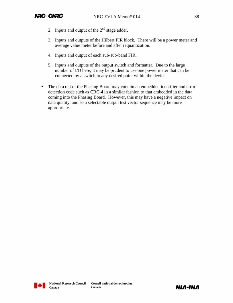
NRC-EVLA Memo# 014 88
National Research CouncilCanada
Conseil national de recherchesCanada
2. Inputs and output of the 2nd stage adder.
3. Inputs and outputs of the Hilbert FIR block. There will be a power meter andaverage value meter before and after requantization.
4. Inputs and output of each sub-sub-band FIR.
5. Inputs and outputs of the output switch and formatter. Due to the largenumber of I/O here, it may be prudent to use one power meter that can beconnected by a switch to any desired point within the device.
• The data out of the Phasing Board may contain an embedded identifier and errordetection code such as CRC-4 in a similar fashion to that embedded in the datacoming into the Phasing Board. However, this may have a negative impact ondata quality, and so a selectable output test vector sequence may be moreappropriate.
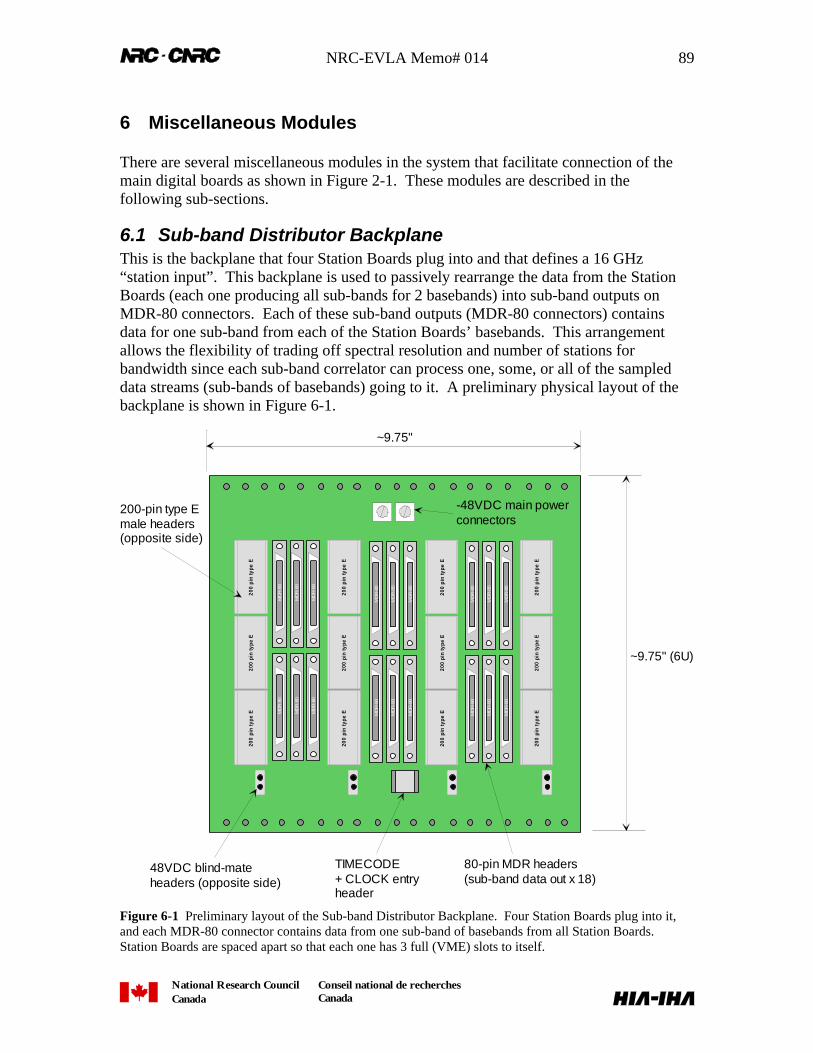
NRC-EVLA Memo# 014 89
National Research CouncilCanada
Conseil national de recherchesCanada
6 Miscellaneous Modules
There are several miscellaneous modules in the system that facilitate connection of themain digital boards as shown in Figure 2-1. These modules are described in thefollowing sub-sections.
6.1 Sub-band Distributor BackplaneThis is the backplane that four Station Boards plug into and that defines a 16 GHz“station input”. This backplane is used to passively rearrange the data from the StationBoards (each one producing all sub-bands for 2 basebands) into sub-band outputs onMDR-80 connectors. Each of these sub-band outputs (MDR-80 connectors) containsdata for one sub-band from each of the Station Boards’ basebands. This arrangementallows the flexibility of trading off spectral resolution and number of stations forbandwidth since each sub-band correlator can process one, some, or all of the sampleddata streams (sub-bands of basebands) going to it. A preliminary physical layout of thebackplane is shown in Figure 6-1.
200
pin
type
E
MD
R-8
0
MD
R-8
0
MD
R-8
0
MD
R-8
0
MD
R-8
0
MD
R-8
0
MD
R-8
0
MD
R-8
0
MD
R-8
0
MD
R-8
0
MD
R-8
0
MD
R-8
0
MD
R-8
0
MD
R-8
0
MD
R-8
0
MD
R-8
0
MD
R-8
0
MD
R-8
0
200
pin
type
E20
0 pi
n ty
pe E
200
pin
type
E20
0 pi
n ty
pe E
200
pin
type
E
200
pin
type
E20
0 pi
n ty
pe E
200
pin
type
E
200
pin
type
E20
0 pi
n ty
pe E
200
pin
type
E
200-pin type Emale headers(opposite side)
80-pin MDR headers(sub-band data out x 18)
-48VDC main powerconnectors
48VDC blind-mateheaders (opposite side)
TIMECODE+ CLOCK entryheader
~9.75" (6U)
~9.75"
Figure 6-1 Preliminary layout of the Sub-band Distributor Backplane. Four Station Boards plug into it,and each MDR-80 connector contains data from one sub-band of basebands from all Station Boards.Station Boards are spaced apart so that each one has 3 full (VME) slots to itself.
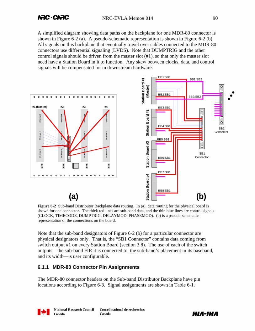
NRC-EVLA Memo# 014 90
National Research CouncilCanada
Conseil national de recherchesCanada
A simplified diagram showing data paths on the backplane for one MDR-80 connector isshown in Figure 6-2 (a). A pseudo-schematic representation is shown in Figure 6-2 (b).All signals on this backplane that eventually travel over cables connected to the MDR-80connectors use differential signaling (LVDS). Note that DUMPTRIG and the othercontrol signals should be driven from the master slot (#1), so that only the master slotneed have a Station Board in it to function. Any skew between clocks, data, and controlsignals will be compensated for in downstream hardware.
200
pin
type
E
MD
R-8
0
200
pin
type
E20
0 pi
n ty
pe E
200
pin
type
E20
0 pi
n ty
pe E
200
pin
type
E
200
pin
type
E20
0 pi
n ty
pe E
200
pin
type
E
200
pin
type
E20
0 pi
n ty
pe E
200
pin
type
E#1 (Master) #2 #3 #4
MD
R-8
0
Sta
tion
Boa
rd #
1(M
aste
r)S
tatio
n B
oard
#2
Sta
tion
Boa
rd #
3S
tatio
n B
oard
#4
MD
R-8
0
BB1:SB1
BB2:SB1
BB3:SB1
BB4:SB1
BB5:SB1
BB6:SB1
BB7:SB1
BB8:SB1
SB1Connector
SB2Connector
BB1:SB2
BB2:SB2
(a) (b)Figure 6-2 Sub-band Distributor Backplane data routing. In (a), data routing for the physical board isshown for one connector. The thick red lines are sub-band data, and the thin blue lines are control signals(CLOCK, TIMECODE, DUMPTRIG, DELAYMOD, PHASEMOD). (b) is a pseudo-schematicrepresentation of the connections on the board.
Note that the sub-band designators of Figure 6-2 (b) for a particular connector arephysical designators only. That is, the “SB1 Connector” contains data coming fromswitch output #1 on every Station Board (section 3.8). The use of each of the switchoutputs—the sub-band FIR it is connected to, the sub-band’s placement in its baseband,and its width—is user configurable.
6.1.1 MDR-80 Connector Pin Assignments
The MDR-80 connector headers on the Sub-band Distributor Backplane have pinlocations according to Figure 6-3. Signal assignments are shown in Table 6-1.
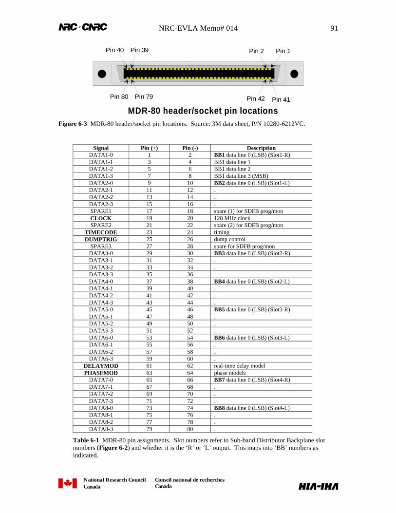
NRC-EVLA Memo# 014 91
National Research CouncilCanada
Conseil national de recherchesCanada
Pin 1Pin 2Pin 39Pin 40
Pin 41Pin 42Pin 79Pin 80
MDR-80 header/socket pin locationsFigure 6-3 MDR-80 header/socket pin locations. Source: 3M data sheet, P/N 10280-6212VC.
Signal Pin (+) Pin (-) DescriptionDATA1-0 1 2 BB1 data line 0 (LSB) (Slot1-R)DATA1-1 3 4 BB1 data line 1DATA1-2 5 6 BB1 data line 2DATA1-3 7 8 BB1 data line 3 (MSB)DATA2-0 9 10 BB2 data line 0 (LSB) (Slot1-L)DATA2-1 11 12 .DATA2-2 13 14 .DATA2-3 15 16 .SPARE1 17 18 spare (1) for SDFB prog/monCLOCK 19 20 128 MHz clockSPARE2 21 22 spare (2) for SDFB prog/mon
TIMECODE 23 24 timingDUMPTRIG 25 26 dump control
SPARE3 27 28 spare for SDFB prog/monDATA3-0 29 30 BB3 data line 0 (LSB) (Slot2-R)DATA3-1 31 32 .DATA3-2 33 34 .DATA3-3 35 36 .DATA4-0 37 38 BB4 data line 0 (LSB) (Slot2-L)DATA4-1 39 40 .DATA4-2 41 42 .DATA4-3 43 44 .DATA5-0 45 46 BB5 data line 0 (LSB) (Slot3-R)DATA5-1 47 48 .DATA5-2 49 50 .DATA5-3 51 52 .DATA6-0 53 54 BB6 data line 0 (LSB) (Slot3-L)DATA6-1 55 56 .DATA6-2 57 58 .DATA6-3 59 60 .
DELAYMOD 61 62 real-time delay modelPHASEMOD 63 64 phase models
DATA7-0 65 66 BB7 data line 0 (LSB) (Slot4-R)DATA7-1 67 68 .DATA7-2 69 70 .DATA7-3 71 72 .DATA8-0 73 74 BB8 data line 0 (LSB) (Slot4-L)DATA8-1 75 76 .DATA8-2 77 78 .DATA8-3 79 80 .
Table 6-1 MDR-80 pin assignments. Slot numbers refer to Sub-band Distributor Backplane slotnumbers (Figure 6-2) and whether it is the ‘R’ or ‘L’ output. This maps into ‘BB’ numbers asindicated.
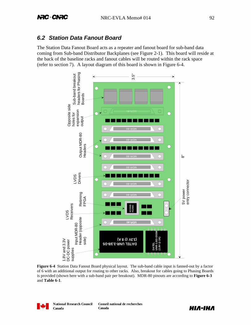
NRC-EVLA Memo# 014 92
National Research CouncilCanada
Conseil national de recherchesCanada
6.2 Station Data Fanout Board
The Station Data Fanout Board acts as a repeater and fanout board for sub-band datacoming from Sub-band Distributor Backplanes (see Figure 2-1). This board will reside atthe back of the baseline racks and fanout cables will be routed within the rack space(refer to section 7). A layout diagram of this board is shown in Figure 6-4.
XC
V50
E-
FG25
6C
DATEL UNR-3.3/8-D5(3.3V @ 8 A)
DA
TEL
UN
R-1
.8/2
-D5S
M(1
.8V
@ 2
A)
MDR-80
MDR-80
MDR-80
MDR-80
MDR-80
MDR-80
1.8V
and
3.3
VD
C-D
C p
ower
supp
lies
Inpu
t MD
R-8
0H
eade
r (op
posi
tesi
de)
LVD
SR
ecei
vers R
etim
ing
FP
GA
LVD
SD
river
sO
utpu
t MD
R-8
0H
eade
rs
Opp
osite
sid
eho
les
for
expa
nsio
nou
tput
Sub
-ban
d br
eako
uthe
ader
s fo
r Pha
sing
Boa
rds
5V p
ower
entry
con
nect
or8"
3.5"
Figure 6-4 Station Data Fanout Board physical layout. The sub-band cable input is fanned-out by a factorof 6 with an additional output for routing to other racks. Also, breakout for cables going to Phasing Boardsis provided (shown here with a sub-band pair per breakout). MDR-80 pinouts are according to Figure 6-3and Table 6-1.
NRC-EVLA Memo# 014 93
National Research CouncilCanada
Conseil national de recherchesCanada
The “Retiming FPGA” resynchronizes the data before re-transmission. This FPGA mustbe programmed and must have its status checked using signals coming from StationBoards as outlined in section 3.10. It may also be desirable/possible to power cycle thisboard by controlling power supply inhibit signals to the DC-DC power supplies. (StatusLEDs, although not shown in the figure, will be provided to allow secondary visualchecks by on-site personnel.) It must also be possible for daisy-chained boards to beprogrammed and monitored in a similar fashion. Finally, since this board contains activecomponents it must be possible to hot-swap it. A straw-man concept of mechanics thatcould facilitate hot-swapping is shown in Figure 6-5.
Inside backpanel ofbaseline rack
Guide posts
Fastening posts
Cableportal
MDR-80entryconnector
SDFBattachmentplate
SDFB PCB(opposite side)
Figure 6-5 Straw-man concept for fastening the Station Data Fanout Board (SDFB) to the inside backpanel of the baseline rack. It must be possible to hot-swap the SDFB without shorting any signals orpower. The guide posts allow the SDFB assembly (includes the PCB and an attachment plate) to be safelyextracted from the panel so that the existing cabling that feeds through the “cable portal” and connects tothe SDFB PCB can be removed. The fastening posts protrude through the attachment plate and are used tofasten the SDFB assembly with wing-nuts. Not shown is a power switch protruding through the SDFBattachment plate to remove +5V power from the PCB.
NRC-EVLA Memo# 014 94
National Research CouncilCanada
Conseil national de recherchesCanada
6.3 Baseline Entry Backplane
This backplane is used to passively feed data from 16 stations/MDR-80 connectors to theBaseline Board. The backplane blind-mateswith the front-entry Baseline Board. Aphysical layout of the backplane is shown inFigure 6-6. In each sub-rack (i.e. “crate” or“card cage”) up to eight of these will bemounted to allow insertion of up to eightBaseline Boards. It is possible that thesecould be formed into one monolithicbackplane, but small individual modulesprovide more flexibility in mixing differentboards in the same sub-rack.
An important consideration is the totalnumber of pins (and more importantly theinsertion force that a large number of pinsdemands) in the connectors that mate withthe Baseline Board. A full discussion ofinsertion force considerations is provided insection 4.5.Figure 6-6 Baseline Entry Backplane physicallayout. This backplane routes signals on the 16 (8‘X’; 8 ‘Y’) input MDR-80 connectors to connectorsthat blind-mate with the front-entry Baseline Board.The MDR-80 connectors are staggered to prevent“pile-up” of cable that is thicker than the connector.
200
pin
type
E20
0 pi
n ty
pe E
200
pin
type
E20
0 pi
n ty
pe E
200
pin
type
E20
0 pi
n ty
pe E
200
pin
type
E
MD
R-8
0
MD
R-8
0
MD
R-8
0
MD
R-8
0
MD
R-8
0
MD
R-8
0
MD
R-8
0
MD
R-8
0
MD
R-8
0
MD
R-8
0
MD
R-8
0
MD
R-8
0
MD
R-8
0
MD
R-8
0
MD
R-8
0
MD
R-8
0
12U(~19.5")
2.5"
MDR-80 station dataentry headers
200-pin type Emale headers(opposite side)
48VDC blind-mateheaders
-48VDC main powerconnectors
NRC-EVLA Memo# 014 95
National Research CouncilCanada
Conseil national de recherchesCanada
6.4 Phasing Board Entry Backplane
This backplane facilitates entry of sub-band data from 48 stations into the Phasing Board.The layout shown in Figure 6-7 contains 48, 36-pin 2.0 mm connectors that mate with
GORE “Eye-opener” cable connectors—each one carries 2 sub-bands, CLOCK,TIMECODE, DELAYMOD, andPHASEMOD coming from a StationData Fanout Board. This preliminarylayout indicates that 48 connectors, eachcontaining a sub-band pair, fit on thebackplane. Thus, it should be possible tophase 2 sub-bands on each PhasingBoard as indicated in section 5. Notethat it may be possible to mate the Eye-opener cable directly with the “200-pintype E” connectors if the 8 rowconfiguration is used.Figure 6-7 Phasing Board Entry Backplanepreliminary layout. This layout supports 48stations and 2 sub-band pairs.
2.5"
12U(~19.5")
200-pin type Emale headers(opposite side)
48 x single station,sub-band pairinput connectors(12 diff. signals)
200
pin
type
E20
0 pi
n ty
pe E
200
pin
type
E20
0 pi
n ty
pe E
200
pin
type
E20
0 pi
n ty
pe E
-48VDC main powerconnectors
48VDC blind-mateheaders
NRC-EVLA Memo# 014 96
National Research CouncilCanada
Conseil national de recherchesCanada
6.5 TIMECODE Generator Box
The TIMECODE Generator Box (TGB) provides the correlator with timing informationthat all operations within the correlator are synchronized to. This box is identified inFigure 2-1.
The TGB has the following inputs:
• Reference clock at some (sub-?) multiple of 128 MHz. A project-wide decision(J. Jackson) has been made to use VLBI standard frequencies, and use of thisfrequency reflects that decision.
• Reference time tick. This should be compatible with TIMECODE (e.g. 1 Hztick).
The TGB has 4836 outputs, each of which is identical and contains the following signals:
• 128 MHz digital clock.
• Four programmable TIMECODE signals. One of these TIMECODEs is the real“wall-clock time”, and three of them are programmable. The parameter spacewithin which the programmable TIMECODEs can be configured is TBD.Nominally, they are to provide non-real-time VLBI capability (possibly with aspeed-up factor as well). Each set of four Station Boards can select one of theTIMECODEs for use.
All outputs are LVDS (probably) using the GORE “Eye-opener” 2.0 mm connectors and50-ohm cable. Routing within the TGB and cables that route signals to Sub-bandDistributor Backplanes should be reasonably well length-matched since any mismatchultimately must be absorbed in the correlator chip. The TGB should be located in thecenter of the correlator station racks.
The TGB will contain an MCB interface module as described in other sections. Thismodule will allow the setting of the TIMECODE epoch synchronous to the inputreference time tick. Communication to the TGB should be such that there is no confusionin the epoch setting.
6.6 Other Modules
Several other modules are required to realize the full functionality that is possible withthe correlator. These modules are indicated in Figure 2-1 and are as follows:
36 It could have more, but this seems to be the number that satisfies the entire EVLA project requirements.
NRC-EVLA Memo# 014 97
National Research CouncilCanada
Conseil national de recherchesCanada
• VLBI recorder interface. This interface synchronizes data from one or morePhasing Boards in preparation for transmission to a VLBI data recorder. Thisinterface is an NRAO responsibility.
• Phased output feedback interface. This interface synchronizes data from one ormore Phasing Boards for feedback, in real time, into the correlator. This interfacemay be combined with the VLBI recorder interface. This interface is an NRAOresponsibility.
• VLBI recorder Station Board interface. This interface is required to feed the datafrom a VLBI recorder (i.e. playback unit) to the Station Board. The straw-manconcept is to always use the fiber-optic receiver module (section 3.1) to importdata into the Station Board. Thus, the VLBI interface would be a unit thatconnects to a VLBI data output unit and produces a fiber-optic signal compatiblewith the fiber-optic receiver module.
• General phased output interface. This interface may be required to allow theoutput from multiple Phasing Boards to be routed to an external data analysissystem. This interface could be integrated with the VLBI recorder interface andoutput feedback interface.
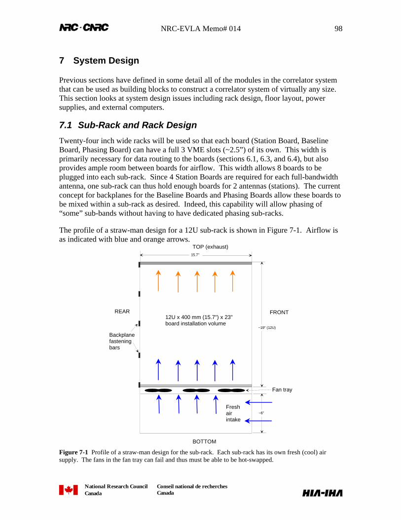
NRC-EVLA Memo# 014 98
National Research CouncilCanada
Conseil national de recherchesCanada
7 System Design
Previous sections have defined in some detail all of the modules in the correlator systemthat can be used as building blocks to construct a correlator system of virtually any size.This section looks at system design issues including rack design, floor layout, powersupplies, and external computers.
7.1 Sub-Rack and Rack Design
Twenty-four inch wide racks will be used so that each board (Station Board, BaselineBoard, Phasing Board) can have a full 3 VME slots (~2.5”) of its own. This width isprimarily necessary for data routing to the boards (sections 6.1, 6.3, and 6.4), but alsoprovides ample room between boards for airflow. This width allows 8 boards to beplugged into each sub-rack. Since 4 Station Boards are required for each full-bandwidthantenna, one sub-rack can thus hold enough boards for 2 antennas (stations). The currentconcept for backplanes for the Baseline Boards and Phasing Boards allow these boards tobe mixed within a sub-rack as desired. Indeed, this capability will allow phasing of“some” sub-bands without having to have dedicated phasing sub-racks.
The profile of a straw-man design for a 12U sub-rack is shown in Figure 7-1. Airflow isas indicated with blue and orange arrows.
~19" (12U)
~6"
12U x 400 mm (15.7") x 23"board installation volume
15.7"
Fan tray
Freshairintake
FRONTREAR
Backplanefasteningbars
TOP (exhaust)
BOTTOM
Figure 7-1 Profile of a straw-man design for the sub-rack. Each sub-rack has its own fresh (cool) airsupply. The fans in the fan tray can fail and thus must be able to be hot-swapped.
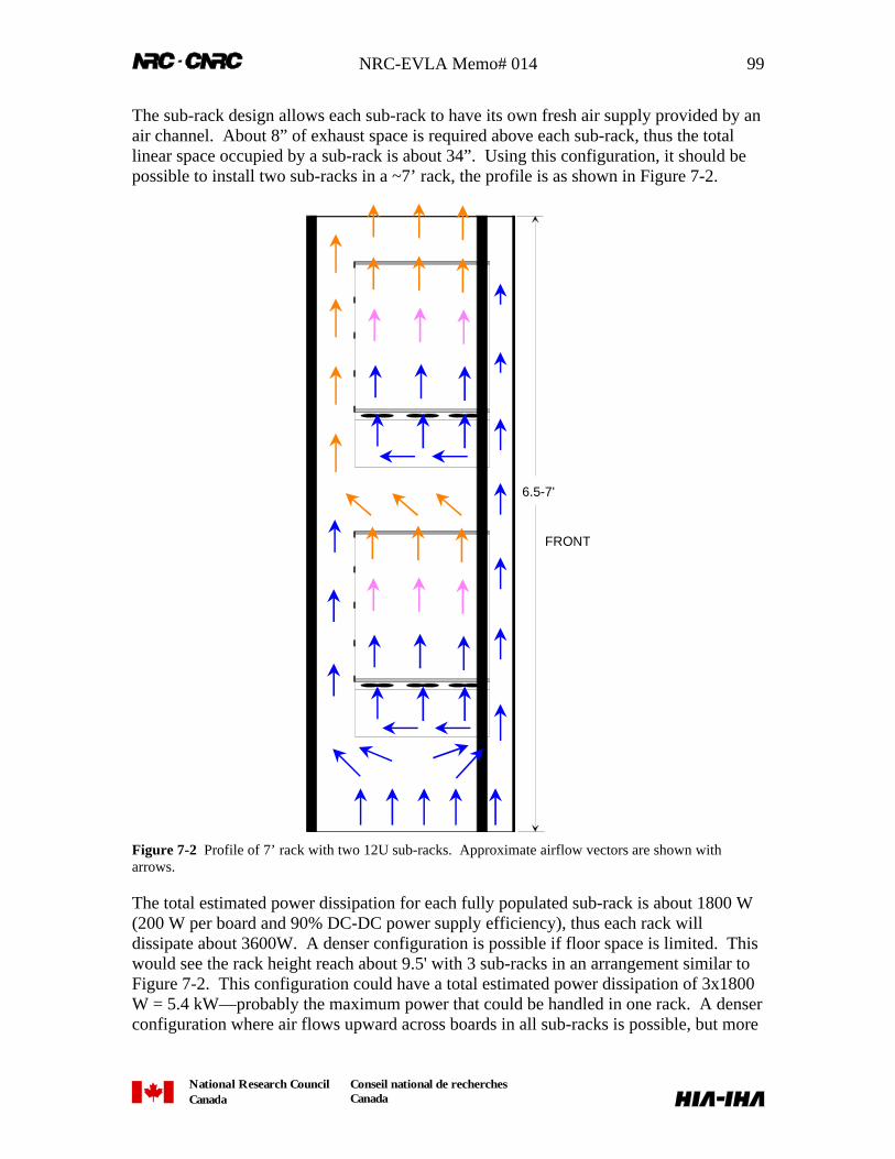
NRC-EVLA Memo# 014 99
National Research CouncilCanada
Conseil national de recherchesCanada
The sub-rack design allows each sub-rack to have its own fresh air supply provided by anair channel. About 8” of exhaust space is required above each sub-rack, thus the totallinear space occupied by a sub-rack is about 34”. Using this configuration, it should bepossible to install two sub-racks in a ~7’ rack, the profile is as shown in Figure 7-2.
6.5-7'
FRONT
Figure 7-2 Profile of 7’ rack with two 12U sub-racks. Approximate airflow vectors are shown witharrows.
The total estimated power dissipation for each fully populated sub-rack is about 1800 W(200 W per board and 90% DC-DC power supply efficiency), thus each rack willdissipate about 3600W. A denser configuration is possible if floor space is limited. Thiswould see the rack height reach about 9.5' with 3 sub-racks in an arrangement similar toFigure 7-2. This configuration could have a total estimated power dissipation of 3x1800W = 5.4 kW—probably the maximum power that could be handled in one rack. A denserconfiguration where air flows upward across boards in all sub-racks is possible, but more
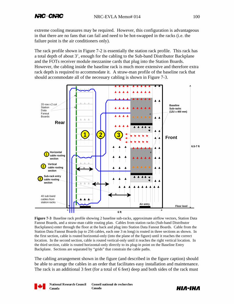
NRC-EVLA Memo# 014 100
National Research CouncilCanada
Conseil national de recherchesCanada
extreme cooling measures may be required. However, this configuration is advantageousin that there are no fans that can fail and need to be hot-swapped in the racks (i.e. thefailure point is the air conditioners only).
The rack profile shown in Figure 7-2 is essentially the station rack profile. This rack hasa total depth of about 3’, enough for the cabling to the Sub-band Distributor Backplaneand the FOTs receiver module mezzanine cards that plug into the Station Boards.However, the cabling inside the baseline rack is much more extensive and therefore extrarack depth is required to accommodate it. A straw-man profile of the baseline rack thatshould accommodate all of the necessary cabling is shown in Figure 7-3.
Floor level
Front
Rear
6 ft
6.5-7 ft
BaselineSub-racks(12U x 400 mm)
Air entry
20 row x 2 colStationDataFanoutBoards
Horizontalcable routingsection
Verticalcable routingsection
Sub-rack entrycable routingsection
40 sub-bandcables fromstation racks
1 2 3
1
2
3
Figure 7-3 Baseline rack profile showing 2 baseline sub-racks, approximate airflow vectors, Station DataFanout Boards, and a straw-man cable routing plan. Cables from station racks (Sub-band DistributorBackplanes) enter through the floor at the back and plug into Station Data Fanout Boards. Cable from theStation Data Fanout Boards (up to 256 cables, each one 3 m long) is routed in three sections as shown. Inthe first section, cable is routed horizontal-only (into the plane of the figure) until it reaches the correctlocation. In the second section, cable is routed vertical-only until it reaches the right vertical location. Inthe third section, cable is routed horizontal-only directly to its plug-in point on the Baseline EntryBackplane. Sections are separated by “grids” that constrain the cable paths.
The cabling arrangement shown in the figure (and described in the figure caption) shouldbe able to arrange the cables in an order that facilitates easy installation and maintenance.The rack is an additional 3 feet (for a total of 6 feet) deep and both sides of the rack must
NRC-EVLA Memo# 014 101
National Research CouncilCanada
Conseil national de recherchesCanada
be accessible (with removable panels) in any correlator configuration. Although this planlooks reasonable on paper, development will include building a full mock-up of thebaseline rack complete with mock cabling to ensure that the plan is indeed feasible.
7.2 Remote Power Control and Monitoring
Each circuit board’s power supply37 in the correlator system will be monitored38 forhealth by using a monitor and control signal provided by the board’s DC-DC converter.This signal is pulled low if the power supply is experiencing some problem (temperature,input voltage, internal parameters etc.). This signal can source ~1.5 mA of current at 5.7VDC, and shorting it to ground with a relay or transistor will shut the DC supply off.Thus, it is possible to remotely control power to each individual circuit board in thesystem. All of the monitor and control lines in each rack will be routed, via associatedbackplanes, to one (DB-25 pin) connector connected to a terminal block as shown inFigure 7-4.
SBDB SBDB
SBDB SBDB
BE
BB
EB
BE
B
BE
BB
EB
BE
B
BE
BP
BE
B
Station Rack Baseline Rack
To monitorand controlcomputer
(PC)
To monitorand controlcomputer
(PC)
Figure 7-4 Routing of DC-DC converter monitor and control lines for each rack. Each rack has a singlecable used for power supply monitor and control.
Each rack thus has a cable coming from it that will be plugged into an external monitorand control card plugged into a computer that is normally not part of correlator systemprocessing and thus less likely to experience crashes from bugs. Also this computer can 37 This may or may not include Station Data Fanout Board DC-DC supplies. However, it will include the48 VDC to 5 VDC power supply that supplies 5 VDC to all Station Data Fanout Boards in a rack.38 In addition to normal board temperature and voltage level monitoring.
NRC-EVLA Memo# 014 102
National Research CouncilCanada
Conseil national de recherchesCanada
be a more expensive and robust model since there will probably only be one of them.PCI cards that perform the sorts of functions required are inexpensive and readilyavailable.
7.3 Correlator Floor Plan
Floor plans for a 40-station and a 48-station correlator have been developed. These plansare shown in Figure 7-5 and Figure 7-6 respectively.
2.5 ft
3 ft
2.5 ft
6 ft
2.5 ft
2.5 ft
3 ft
4 ft
2.5 ft
StationRack
BaselineRack
7 ft
7 ft
18.5 ft
Max cable length ~= 32.5 ft (10 m)
48 VDCRectifier
Plant(100-150 kW)
48 VDCBatteryPlant
(6.5 ft x26.4 in;767.3
lbs/ft^2)
2.5 ft
2.5 ft
2.5 ft
2.5 ft
35 ft
43 ft
5 ft
Possible under-the-floorground plane
Fib
er-o
ptic
s ra
cks
and
othe
r eq
uipm
ent
Air Conditioner
Air Conditioner
Figure 7-5 Possible 40-station correlator floor plan. The station racks are in the center of all of the rackssince cable from each station rack goes to every baseline rack, each cable must be the same length, and it isdesirable to minimize the cable lengths. The floor plan has dimensions of 35 x 43 ft, and there is enoughroom for additional racks of equipment. Data output processing computers could be mounted in racks orshelves beside each baseline rack so as not to interfere with access to baseline rack cabling. The location ofthe TIMECODE Generator Box is not yet defined, but it can probably be located in one of the centralstation racks.
NRC-EVLA Memo# 014 103
National Research CouncilCanada
Conseil national de recherchesCanada
50 ft
45 ftStation Racks (12)
Air Conditioner
Air Conditioner
Air
Con
ditio
ner
Air
Con
ditio
ner
Air
Con
ditio
ner
Air
Con
ditio
ner
26 ft+14ft = 40 ft = 12.2 m
7 ft
7 ft
3 racks =2 sub-bandcorrelators
Baseline Racks (24)
48 VDCRectifier
Plant(100-150 kW)
48 VDCBatteryPlant
(6.5 ft x26.4 in;767.3
lbs/ft^2)
Fib
er-o
ptic
s ra
cks
and
othe
r eq
uipm
ent
2.5 ft 3 ft
2.5 ft3 ft
2.5 ft
2.5 ft
Possible under-the-floorground plane
Figure 7-6 Possible 48-station correlator floor plan. In this arrangement, 3 baseline racks contain all ofthe boards for 2 sub-band correlators and so there are a total of 1.5 x 16 = 24 baseline racks. The stationracks are in the center of all of the racks since cable from each station rack goes to every baseline rack,each cable must be the same length, and it is desirable to minimize the cable lengths. The floor plan hasdimensions of 45 x 50 ft, and there is enough room for additional racks of equipment. Data outputprocessing computers could be mounted in racks or shelves beside each baseline rack so as not to interferewith access to baseline rack cabling. The location of the TIMECODE Generator Box is not yet defined, butit can probably be rack-mounted in one of the central station racks.
The racks will be installed on a raised floor and all cabling will route under the floor.The air conditioners will pressurize the floor and each rack will draw cold air from thefloor. Because of cabling and the uneven distribution of air conditioners and racks, therewill be pressure gradients across the installation. NRAO has requested that each rackhave an adjustable vent at the bottom so that airflow can be properly equalized. It is notyet known whether or not additional fans will be installed at the bottom of each rack.
NRC-EVLA Memo# 014 104
National Research CouncilCanada
Conseil national de recherchesCanada
An artist’s rendering of a 48-station correlator installation (not including the mains 48 Vsupply or other racks) is shown in Figure 7-7.
Station Racks
Baseline RacksAir Conditioners
Figure 7-7 Artist’s rendering of the 48-station correlator installation.
The “under-the-floor” ground plane in Figure 7-5 and Figure 7-6 is a low-impedance pathfor shunting common-mode currents that may flow from rack to rack. Backplanegrounds (that connect to circuit board grounds) are bonded to sub-racks, sub-racks arebonded to racks, and the racks are bonded to this ground plane. The ground plane is usedin conjunction with common-mode filters39 on the sub-band cables that travel fromstation racks to baseline racks. That is, the proposed noise attenuation method is to bothfilter and shunt common-mode noise so that it does not travel on the differential signallines that connect boards in different racks. Since the correlator will be installed in ascreened room, the ground plane can probably be the inside floor of the screened room.
The correlator will take its power from a 48 VDC power plant. By doing this, single-point power supply failures are isolated to a single circuit board that can easily becontrolled and hot-swapped as described in previous sections. The 48 VDC plant is atelephony central office-grade supply that contains redundancy so that any failure can be
39 These filters will probably be installed on entry to the Station Data Fanout Board.
NRC-EVLA Memo# 014 105
National Research CouncilCanada
Conseil national de recherchesCanada
detected and replaced on-line. The hold-time requirement for this plant in the event of anAC power failure is 15 minutes. The power plant manufacturer will be consultedregarding the best method for routing DC power to each rack.
The planned hardware delivered by NRC is everything for a 32-station correlator, withracks for 40 stations. There is a strong indication, however, that the full EVLAexpansion correlator will require 48 stations and thus the system design must allow forthis eventuality.
7.4 Correlator Computing
7.4.1 Hardware Configuration
The system module diagram of Figure 2-1 shows Station Boards, Phasing Boards, andBaseline Boards connecting to external control and data processing computers. Each ofthe boards has an MCB/CPU mezzanine card mounted on it with a bus interface forcommunication with on-board devices, and an Ethernet interface for communication withthe external computers. In addition, each Baseline Board has a Front Panel Data Port(FPDP) interface that pipes correlated data to a back-end computer.
The straw-man concept for the control and back-end computers is to use COTS PC boxesrunning Linux since they offer a high performance-to-price ratio in a generic package.These boxes can easily be upgraded to the latest performance machine with minimalimpact on software as long as Ethernet and FPDP interface cards continue to be available,and as long as the software is written so that it is loosely coupled to the hardwareplatform. This should be possible since all of the “hard” real-time control software willreside on the MCB mezzanine cards. The computers with the FPDP interfaces will seedata frames coming from Baseline Boards (section 4.3), that get processed and/orbuffered as they arrive without any special real-time processing requirements. Thesecomputers write FITS file fragments to network disks—these fragments get “vacuumedup” by downstream image/archive processing computers.
The current estimate (ref: Aug. 27-28/01 meeting in Socorro) is that 1 computer will berequired for Station Board control and 1 to 4 computers will be required for BaselineBoard and Phasing Board control. The number of computers required to handle FPDPdata is scaleable, but the straw-man plan is to use 1 computer for every 4 BaselineBoards, and to arrange these computers in multiple Beowulf clusters. A simplifieddiagram of the correlator computing environment is shown in Figure 7-8.
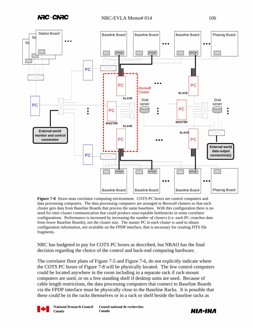
NRC-EVLA Memo# 014 106
National Research CouncilCanada
Conseil national de recherchesCanada
Station Board
Baseline Board
FPDP
PC
Phasing BoardStation Board
Station Board Baseline Board
FPDP
PC
PC
Baseline Board
FPDP
PC
Baseline Board
FPDP
Phasing BoardBaseline Board
FPDP
PC
PC
Baseline Board
FPDP
PC
Diskserver
Diskserver
BeowulfCluster
External worldmonitor and control
connection
External worlddata output
connection(s)
PC PC
MASTERSLAVE
SLAVE
MASTER
SLAVE
SLAVE
Figure 7-8 Straw-man correlator computing environment. COTS PC boxes are control computers anddata processing computers. The data processing computers are arranged in Beowulf clusters so that eachcluster gets data from Baseline Boards that process the same baselines. With this configuration there is noneed for inter-cluster communication that could produce unacceptable bottlenecks in some correlatorconfigurations. Performance is increased by increasing the number of clusters (i.e. each PC crunches datafrom fewer Baseline Boards), not the cluster size. The master PC in each cluster is used to obtainconfiguration information, not available on the FPDP interface, that is necessary for creating FITS filefragments.
NRC has budgeted to pay for COTS PC boxes as described, but NRAO has the finaldecision regarding the choice of the control and back-end computing hardware.
The correlator floor plans of Figure 7-5 and Figure 7-6, do not explicitly indicate wherethe COTS PC boxes of Figure 7-8 will be physically located. The few control computerscould be located anywhere in the room including in a separate rack if rack-mountcomputers are used, or on a free standing shelf if desktop units are used. Because ofcable length restrictions, the data processing computers that connect to Baseline Boardsvia the FPDP interface must be physically close to the Baseline Racks. It is possible thatthese could be in the racks themselves or in a rack or shelf beside the baseline racks as
NRC-EVLA Memo# 014 107
National Research CouncilCanada
Conseil national de recherchesCanada
long as the location does not cause high-speed intra-cabinet cable access problems. Finaldetails are TBD.
7.4.2 Software Configuration
The “correlator software” is roughly defined as any software that resides inside theboundaries shown in Figure 7-8. The external world has access points40 for monitor andcontrol of the correlator, and for data output as identified in the figure. These accesspoints form an interface that has become known as the “Virtual Correlator Interface”(VCI). All of the details of how to configure the correlator and all of the real-timeprocessing necessary to run the correlator lie below the VCI. The level of functionality,communications protocols, and internal details of the correlator software is TBD.
40 There is another access point for remote power cycling independent of any correlator control computer(sections 3.10, 7.2).
NRC-EVLA Memo# 014 108
National Research CouncilCanada
Conseil national de recherchesCanada
8 References
[0] Carlson, B., A Proposed WIDAR Correlator for the Expansion Very Large ArrayProject: Discussion of Capabilities, Implementation, and Signal Processing, NRC-EVLAMemo# 001, May 18, 2000.
[1] Carlson, B., Requirements for 8-bit Processing in the Proposed WIDAR Correlatorfor the EVLA, NRC-EVLA Memo# 010, January 29, 2001.
[2] Carlson, B.R., Dewdney, P.E., Burgess, T.A., Casorso, R.V., Petrachenko, W.T.,Cannon, W.H., The S2 VLBI Correlator: A Correlator for Space VLBI and GeodeticSignal Processing, Publications of the Astronomical Society of the Pacific, 1999, 111,1025-1047.
[3] Carlson, B., Simulation Tests of Sub-Sample Delay Tracking in the ProposedWIDAR Correlator for the Expanded Very Large Array, NRC-EVLA Memo# 007,October 3, 2000.
[4] Carlson, B., Dewdney, P., Simulation Tests to Quantify the Spectral Dynamic Rangeand Narrowband Interference Robustness of the WIDAR Correlator for the EVLA, NRC-EVLA Memo# 009, November 1, 2000.
[5] Carlson, B., Two Correlators for the Price of One: How a VLBA Correlator Could FitWithin the Proposed 40-Station WIDAR EVLA Correlator, NRC-EVLA Memo# 006,September 28, 2000.
[6] Carlson, B., An Analysis of the Effects of Phase Dithering in a Lag-based Fringe-Stopping XF Correlator, NRC-EVLA Memo# 002, May 26, 2000.
[7] Whitney, A.R., 1982, The Mark III Correlator: Design, Operation, and Productivity inProc. IAG Symp. 5, Geodetic Applications of Radio Interferometry (NOAA Tech. Rep.NOS 95) (Rockville: NOAA), 152.
[8] Carlson, B., A Closer Look at 2-Stage Digital Filtering in the Proposed WIDARCorrelator for the EVLA, NRC-EVLA Memo# 003, June 29, 2000.
[9] Carlson, B., Simulation Tests of Phasing Subsystem Signal Processing in the WIDARCorrelator for the EVLA, NRC-EVLA Memo# 008, November 7, 2000.
NRC-EVLA Memo# 014 109
National Research CouncilCanada
Conseil national de recherchesCanada
Index
440-station
floor plan, 10248 VDC, 10448-station
floor plan, 1034X CCQ Lag Correlator Array, 61
77-bit Requantization and Correlation
essential elements, 24
Aair conditioners, 100, 103Airflow, 98airflow vectors, 99, 100anti-aliasing, 11artist’s rendering
correlator installation, 104autocorrelator
"synthetic", 20Autocorrelator
wideband, 20
BBandwidth, 11baseband pair, 13Baseline Board, 12, 13
block diagram, 28high-speed data routing paths, 80main section, 27physical layout, 78rear-side physical layout, 79
Baseline Board Physical Layoutmain section, 77
Baseline Entry Backplanemain section, 94
baseline rack, 100BERT, 17, 18, 20Bit Error Rate Test, 17
Ccapabilities, 11CCID, 72, 75CCQ, 53CLOCK, 32CLRS, 38Coarse Delay Module, 19common-mode noise, 104complex phase rotation, 52correlation holdoff, 38
correlator chipaccumulator size, 64and recirculation, 55detailed functional description, 54dump control, 55dump overun, 55LTA interface, data frame, 60
Correlator Chipblack-box description, 55main section, 52
Correlator Chip Block Diagram, 58correlator chip CCQ
block diagram, 63Correlator Chip Quad
diagram, 54Correlator Chip Quads, 53correlator chips
matrix, 13Correlator Computing
main section, H/W, S/W, 105correlator computing environment, 105Correlator Floor Plan, 102correlator network environment, 106COTS, 66, 105, 106CRC-4, 32, 34, 35, 88
Ddata bias
corr chip, 61data frame
corr chip, 60less than 128 lags, 61
data output capability, 11Data Path Switch
Station Board, 18data valid flagging
no restrictions, 24DC[0:3], 38DC-DC converter
power control+monitoring, 101DELAY, 36delay center, 11Delay Generator
on Station Board, 20delay tracking, 11DELAY_FRAME, 36DELAYMOD, 17, 20, 25, 33, 34, 85, 90, 91, 95delay-path differences
correlator chip, 54de-scoping
FIR, number of bits, 21deskew, 41digital filters
number of, 11DLL, 40, 41DUMP_EN[0:7], 36DUMP_ENx control bits, 38DUMP_SYNC, 36
NRC-EVLA Memo# 014 110
National Research CouncilCanada
Conseil national de recherchesCanada
DUMPTRIG, 17, 25, 33, 38, 48, 49, 50, 51, 68, 70, 90,91
DVALID, 36
Eejector handles
Baseline Board, 77error checking, 29Ethernet, 14, 27, 105expansion, 14External blanking
into Station Board, 26
Ffiber-optic links, 12fiber-optics, 12Fine Delay Controller, 19
Station Board, 19FIR filter banks, 13FIR Filter Banks, 21firmware
FPGA, 24FITS, 105, 106Flexibilities, 14FOTs Rx Module
to Station Board interface, 18FOTS Rx Module(s), 17FPDP, 13
ANSI/VITA standard, 66multiple interfaces, 67scaleable performance, 66
FPDP bus routing, 82FPDP drivers, 81FPDP interface
routing, multiple interfaces, 83FPDP Scheduler and TM
functional timing diagram, 69FPDP Scheduler FPGA, 68
main section, 77FRAME_ABORT*, 56frequency synthesizers, 20fringe stopping
5-level, 53Front Panel Data Port, 13Front Panel Data Port Interface
LTA Controller, 65
GGORE, 95, 96ground plane
correlator installation, 104
HHarmonic suppression phase, 38Hilbert FIR, 86
performance, 86hot-swap, Baseline Board
procedure, 30HSP[0:3], 38
Iidentification information, 25insertion/extraction force, 77
mitigation, 78in-system programmable
FPGAs, 21interleaved sampler, 11
LLag Block number, 43Lag numbering
correlator chip, 52Linux, 105LO shifting
reasons for, 11LTA, 13, 69
memory map, 75LTA Controller, 13
black-box diagram, 66corr chip interface, 56detailed functional description, 71functional block diagram, 73main description, 65performance estimates, 72top-level schematic, paper design, 74
LTA Controller functionsintegrate in corr chip, 65
LTA controller interface functional timing, 57LTA dump data frame, 70LTA Frame Output Controller, 71LTA Integration Controller, 72LTA memory, 50LTA memory addressing, 76LTA RAM, 13LTA RAM memory map, 75LTA Semaphore Table, 71LUT
FIR, 21LVDS, 31, 90, 96LVTTL, 31
MMCB interface
corr chip, 57MCB Interface Module, 27MCB mezzanine card, 14MDR-80
connector, 26, 89, 90, 91, 92, 94memory buffer
circular, 43mezzanine card
delay, 13mezzanine cards
fiber-optic, 12Miscellaneous Modules
NRC-EVLA Memo# 014 111
National Research CouncilCanada
Conseil national de recherchesCanada
main section, 89mock-up
baseline rack, 101module connectivity diagram, 12multi-beaming, 11, 22multi-beaming, sub-band
coherence loss, 23delay tracking, 23delay tracking, alternative, 24equation, 22very long baselines, 23
NNarrowband Radar Filter, 21noise diode switching
synchronization, 21Normal Dumping Real-Time Control, 50NRAO, 12, 14, 17, 27, 87, 97, 103, 106
OOther Modules, 96Output Cross-Bar Switch and Pulsar Timing
Station Board, 25Output Data Frame Formats
on FPDP interface, 69output data rate, 11
PPB[0:15], 38PCI, 66, 102performance requirements
dumping, bottlenecks, 82phase matching
clock, across system, 29phase rotation, 52Phased output feedback interface, 97phased output interface, 97phased-VLA, 11
bandwidth, 11phased-VLA beams
multi-beaming, 22PHASEMOD, 17, 23, 25, 33, 34, 35, 85, 90, 91, 95PHASEO[0:7][0:3], 35Phasing Board, 12, 13
2nd stage sub-array adder, 864-station mixer, 1st stage adder, 857-bit requantization, 24error detection, 87features, 85main section, 84output switch and formatting, 87sub-sub-band FIR filter bank, 87
Phasing Board block diagram, 84Phasing Board Entry Backplane, 13
main section, 95ping-pong
recirculation memory, 30poly-phase
FIR, 21poly-phase FIR/FFT
filter bank, alternative, 22Power Control and Monitoring
remote, 101power dissipation
sub-rack, rack, 99power plant
48 VDC, 104PPS, 18pseudo-random code, 40Pulsar Phase Binning and Recirculation, 51Pulsar Phase Binning Real-Time Control, 50Pulsar processing
capability, 11pulsar timer and gate generators, 25
RRadar-mode
capability, 11RECIRC_BLK, 36recirculation
and phase binning, 49capability, 11control and synchronization issues, 48integration time smearing, 46LTA phase bin tradeoff, 49normal dumping, 50timestamp skew, 44
Recirculationoperation description, 42
recirculation algorithm, 48Recirculation Controller, 27
7-bit correlation req's, 24black box diagram, 31block diagram, 39functional timing, 37input signal definition, 31input timing and synchronization, 40main functions, 40main section, 30outputs to correlator chips, 35
Recirculation Controllers, 13recirculation memory, 30Recirculation Real-Time Control, 48recirculation synchronization, 48Ref/Cal Filter, 21RFI robustness, 11
Ssampled basebands, 13sampler demultiplexer
poly-phase FIR/FFT, 22SCHID_FRAME*, 36science and system requirements, 11SDATA format, 32SDATAO[0:7][0:3], 35SDRAM, 19, 27, 28, 29, 65, 66, 71, 72, 73, 75, 76, 79SE_CLK[0:7], 35Shift Enable Clock, 35
NRC-EVLA Memo# 014 112
National Research CouncilCanada
Conseil national de recherchesCanada
spectral channelscapability, 11
spectral dynamic range, 11speed dump
output data format, 69Speed dump data frame, 71speed dumping
performance estimates, 72Station Board, 12
block diagram, 16main description, 16master, 12
Station Boardsslave, 13
Station Data Fanout Boardmain section, 92mechanical design, for hot-swapping, 93physical layout, 92programming, 26
Station Data Fanout Boards, 13stiffener plate
Baseline Board, 77stitch
sub-bands, 21sub-arraying, 11sub-band
multi-beaming, 11sub-band cable output
simplified definition, 13Sub-band Distributor Backplane, 13
data routing, 90main section, 89
Sub-band Multi-beaming, 22Sub-Rack and Rack Design
main section, 98sub-sub-bands
phased output, 84System Design
main section, 98System Overview, 12
Ttap coefficients, 21, 24Temperature
monitoring, 26Test Vector Generator, 40TGB, 96thermal protection
dead-man, 26TIMECODE, 18, 20, 21, 25, 32, 33, 34, 35, 36, 37, 48,
90, 91, 95, 96, 102, 103TIMECODE Generator Box, 96time-skew removal, 32TIMESTAMP, 36
VVCI, 107Vernier Delay Generator
corr chip, 59Virtual Correlator Interface, 107VLBA antennas
correlated with VLA antennas, 53VLBI Mode Phase Modifier
corr chip, 59VLBI recorder interface, 97VLBI recorder Station Board interface, 97voltage
monitoring, 26
Wwavefront delay, 17wavelength demodulated, 12WIDAR, 1, 2, 13, 33, 34, 59, 108wide-band recirculation
sensitivity loss, 47special case
concatenate lags, 47time-burst diagram, 47
Wideband recirculation, 11Wide-band Recirculation
main description, 47
XX and Y station data streams
final synchronization, 29