Embed Size (px)
Citation preview
September 2017 DocID2149 Rev 23 1/27
This is information on a product in full production. www.st.com
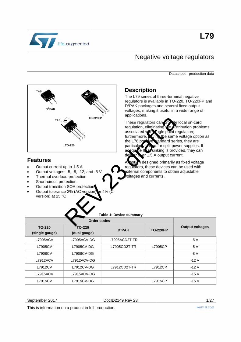
L79
Negative voltage regulators
Datasheet - production data
Features Output current up to 1.5 A
Output voltages: -5, -8, -12, and -5 V
Thermal overload protection
Short-circuit protection
Output transition SOA protection
Output tolerance 2% (AC version) or 4% (Cversion) at 25 °C
Description The L79 series of three-terminal negative regulators is available in TO-220, TO-220FP and D²PAK packages and several fixed output voltages, making it useful in a wide range of applications.
These regulators can provide local on-card regulation, eliminating the distribution problems associated with single point regulation; furthermore, having the same voltage option as the L78 positive standard series, they are particularly suited for split power supplies. If adequate heat sinking is provided, they can deliver over 1.5 A output current.
Although designed primarily as fixed voltage regulators, these devices can be used with external components to obtain adjustable voltages and currents.
Table 1: Device summary
Order codes
Output voltages TO-220
(single gauge)
TO-220
(dual gauge) D²PAK TO-220FP
L7905ACV L7905ACV-DG L7905ACD2T-TR -5 V
L7905CV L7905CV-DG L7905CD2T-TR L7905CP -5 V
L7908CV L7908CV-DG -8 V
L7912ACV L7912ACV-DG -12 V
L7912CV L7912CV-DG L7912CD2T-TR L7912CP -12 V
L7915ACV L7915ACV-DG -15 V
L7915CV L7915CV-DG L7915CP -15 V
12
3
TO-220
TAB
12
3
TO-220FP
13
TAB
D PAK2
REV 23 dr
aft a
Contents L79
2/27 DocID2149 Rev 23
Contents
1 Diagram ............................................................................................ 5
2 Pin configuration ............................................................................. 6
3 Maximum ratings ............................................................................. 7
4 Test circuit ....................................................................................... 8
5 Electrical characteristics ................................................................ 9
6 Application information ................................................................ 14
7 Package information ..................................................................... 16
7.1 TO-220 (single gauge) package information ................................... 16
7.2 TO-220 (dual gauge) package information ...................................... 18
7.3 TO-220FP package information ...................................................... 20
7.4 D²PAK (TO-263) type A package information ................................. 22
7.5 D²PAK type A packing information .................................................. 24
8 Revision history ............................................................................ 26
REV 23 dr
aft a
L79 List of tables
DocID2149 Rev 23 3/27
List of tables
Table 1: Device summary ........................................................................................................................... 1 Table 2: Absolute maximum ratings ........................................................................................................... 7 Table 3: Thermal data ................................................................................................................................. 7 Table 4: Electrical characteristics of L7905AC ........................................................................................... 9 Table 5: Electrical characteristics of L7905C ............................................................................................. 9 Table 6: Electrical characteristics of L7908C ........................................................................................... 10 Table 7: Electrical characteristics of L7912AC ......................................................................................... 11 Table 8: Electrical characteristics of L7912C ........................................................................................... 11 Table 9: Electrical characteristics of L7915AC ......................................................................................... 12 Table 10: Electrical characteristics of L7915C ......................................................................................... 13 Table 11: TO-220 (single gauge) package mechanical data .................................................................... 17 Table 12: TO-220 type A package mechanical data ................................................................................ 19 Table 13: TO-220FP package mechanical data ....................................................................................... 21 Table 14: D²PAK (TO-263) type A package mechanical data .................................................................. 22 Table 15: D²PAK type A tape and reel mechanical data .......................................................................... 25 Table 16: Document revision history ........................................................................................................ 26
REV 23 dr
aft a
List of figures L79
4/27 DocID2149 Rev 23
List of figures
Figure 1: Schematic diagram ...................................................................................................................... 5 Figure 2: Pin connections (top view) ........................................................................................................... 6 Figure 3: Test circuit ................................................................................................................................... 8 Figure 4: Fixed output regulator ................................................................................................................ 14 Figure 5: Split power supply (±15 V - 1 A) ................................................................................................ 14 Figure 6: Circuit for increasing output voltage .......................................................................................... 14 Figure 7: High current negative regulator (-5 V / 4 A with 5 A current limiting) ........................................ 15 Figure 8: TO-220 (single gauge) package outline .................................................................................... 16 Figure 9: TO-220 type A package outline ................................................................................................. 18 Figure 10: TO-220FP package outline...................................................................................................... 20 Figure 11: D²PAK (TO-263) type A package outline ................................................................................ 22 Figure 12: D²PAK (TO-263) type A recommended footprint (dimensions are in mm) .............................. 23 Figure 13: D²PAK type A tape outline ....................................................................................................... 24 Figure 14: D²PAK type A reel outline ........................................................................................................ 25
REV 23 dr
aft a
L79 Diagram
DocID2149 Rev 23 5/27
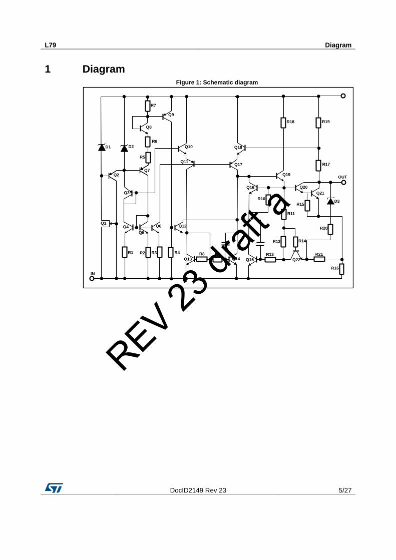
1 Diagram Figure 1: Schematic diagram
R1 R2 R3 R4
R5
R6
R7
R8 R9
R10
R11
R12
R13
R14
R15
R16
R17
R18 R19
R20
R21
Q1
Q2
Q3
Q4
Q5
Q6
Q7
Q8
Q9
Q10
Q11
Q12
Q13 Q14
Q16
Q17
Q18
Q19
Q20
Q21
Q22Q15
D1 D2
D3
OUT
IN
REV 23 dr
aft a
Pin configuration L79
6/27 DocID2149 Rev 23
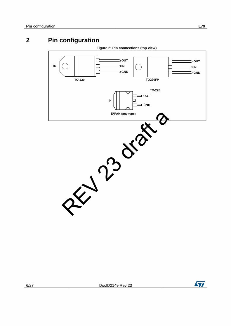
2 Pin configuration Figure 2: Pin connections (top view)
TO-220
D²PAK (any type)
IN
TO220FPTO-220
OUT
IN
GND
OUT
IN
GND
REV 23 dr
aft a
L79 Maximum ratings
DocID2149 Rev 23 7/27
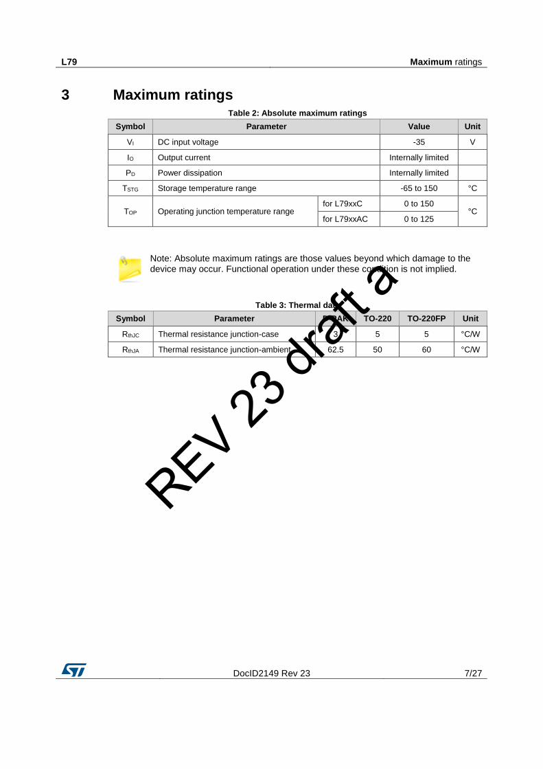
3 Maximum ratings Table 2: Absolute maximum ratings
Symbol Parameter Value Unit
VI DC input voltage -35 V
IO Output current Internally limited
PD Power dissipation Internally limited
TSTG Storage temperature range -65 to 150 °C
TOP Operating junction temperature range for L79xxC 0 to 150
°C for L79xxAC 0 to 125
Note: Absolute maximum ratings are those values beyond which damage to the device may occur. Functional operation under these condition is not implied.
Table 3: Thermal data
Symbol Parameter D²PAK TO-220 TO-220FP Unit
RthJC Thermal resistance junction-case 3 5 5 °C/W
RthJA Thermal resistance junction-ambient 62.5 50 60 °C/W
REV 23 dr
aft a
Test circuit L79
8/27 DocID2149 Rev 23
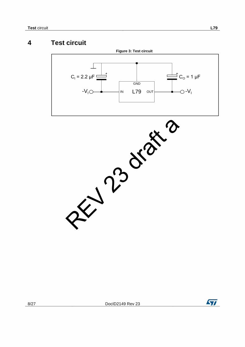
4 Test circuit Figure 3: Test circuit
-VI IN
GND
OUTL79
CO = 1 µFCI = 2.2 µF
-VI
REV 23 dr
aft a
L79 Electrical characteristics
DocID2149 Rev 23 9/27
5 Electrical characteristics
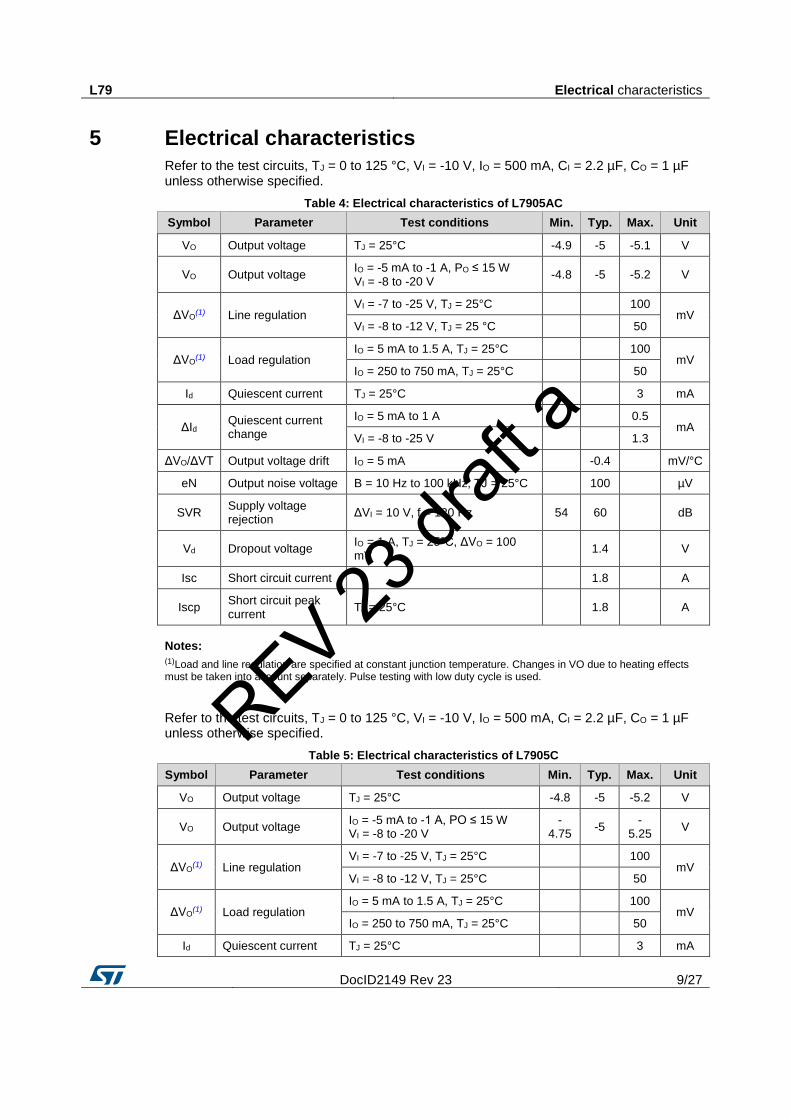
Refer to the test circuits, TJ = 0 to 125 °C, VI = -10 V, IO = 500 mA, CI = 2.2 µF, CO = 1 µF unless otherwise specified.
Table 4: Electrical characteristics of L7905AC
Symbol Parameter Test conditions Min. Typ. Max. Unit
VO Output voltage TJ = 25°C -4.9 -5 -5.1 V
VO Output voltage IO = -5 mA to -1 A, PO ≤ 15 W VI = -8 to -20 V
-4.8 -5 -5.2 V
ΔVO(1) Line regulation
VI = -7 to -25 V, TJ = 25°C
100 mV
VI = -8 to -12 V, TJ = 25 °C
50
ΔVO(1) Load regulation
IO = 5 mA to 1.5 A, TJ = 25°C
100 mV
IO = 250 to 750 mA, TJ = 25°C
50
Id Quiescent current TJ = 25°C
3 mA
ΔId Quiescent current change
IO = 5 mA to 1 A
0.5 mA
VI = -8 to -25 V
1.3
ΔVO/ΔVT Output voltage drift IO = 5 mA
-0.4
mV/°C
eN Output noise voltage B = 10 Hz to 100 kHz, TJ = 25°C
100
µV
SVR Supply voltage rejection
ΔVI = 10 V, f = 120 Hz 54 60
dB
Vd Dropout voltage IO = 1 A, TJ = 25°C, ΔVO = 100 mV
1.4
V
Isc Short circuit current
1.8
A
Iscp Short circuit peak current
TJ = 25°C
1.8
A
Notes:
(1)Load and line regulation are specified at constant junction temperature. Changes in VO due to heating effects must be taken into account separately. Pulse testing with low duty cycle is used.
Refer to the test circuits, TJ = 0 to 125 °C, VI = -10 V, IO = 500 mA, CI = 2.2 µF, CO = 1 µF unless otherwise specified.
Table 5: Electrical characteristics of L7905C
Symbol Parameter Test conditions Min. Typ. Max. Unit
VO Output voltage TJ = 25°C -4.8 -5 -5.2 V
VO Output voltage IO = -5 mA to -1 A, PO ≤ 15 W VI = -8 to -20 V
-4.75
-5 -
5.25 V
ΔVO(1) Line regulation
VI = -7 to -25 V, TJ = 25°C
100 mV
VI = -8 to -12 V, TJ = 25°C
50
ΔVO(1) Load regulation
IO = 5 mA to 1.5 A, TJ = 25°C
100 mV
IO = 250 to 750 mA, TJ = 25°C
50
Id Quiescent current TJ = 25°C
3 mA
REV 23 dr
aft a
Electrical characteristics L79
10/27 DocID2149 Rev 23
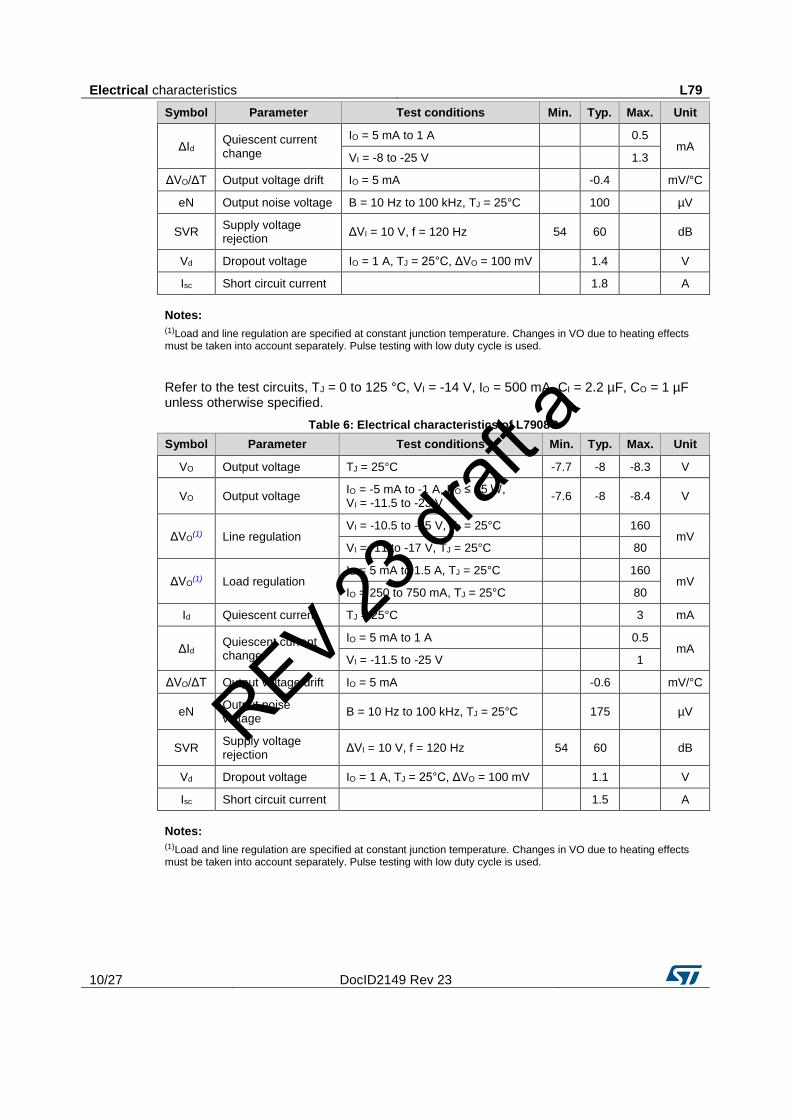
Symbol Parameter Test conditions Min. Typ. Max. Unit
ΔId Quiescent current change
IO = 5 mA to 1 A
0.5 mA
VI = -8 to -25 V
1.3
ΔVO/ΔT Output voltage drift IO = 5 mA
-0.4
mV/°C
eN Output noise voltage B = 10 Hz to 100 kHz, TJ = 25°C
100
µV
SVR Supply voltage rejection
ΔVI = 10 V, f = 120 Hz 54 60
dB
Vd Dropout voltage IO = 1 A, TJ = 25°C, ΔVO = 100 mV
1.4
V
Isc Short circuit current
1.8
A
Notes:
(1)Load and line regulation are specified at constant junction temperature. Changes in VO due to heating effects must be taken into account separately. Pulse testing with low duty cycle is used.
Refer to the test circuits, TJ = 0 to 125 °C, VI = -14 V, IO = 500 mA, CI = 2.2 µF, CO = 1 µF unless otherwise specified.
Table 6: Electrical characteristics of L7908C
Symbol Parameter Test conditions Min. Typ. Max. Unit
VO Output voltage TJ = 25°C -7.7 -8 -8.3 V
VO Output voltage IO = -5 mA to -1 A, PO ≤ 15 W, VI = -11.5 to -23 V
-7.6 -8 -8.4 V
ΔVO(1) Line regulation
VI = -10.5 to -25 V, TJ = 25°C
160 mV
VI = -11 to -17 V, TJ = 25°C
80
ΔVO(1) Load regulation
IO = 5 mA to 1.5 A, TJ = 25°C
160 mV
IO = 250 to 750 mA, TJ = 25°C
80
Id Quiescent current TJ = 25°C
3 mA
ΔId Quiescent current change
IO = 5 mA to 1 A
0.5 mA
VI = -11.5 to -25 V
1
ΔVO/ΔT Output voltage drift IO = 5 mA
-0.6
mV/°C
eN Output noise voltage
B = 10 Hz to 100 kHz, TJ = 25°C
175
µV
SVR Supply voltage rejection
ΔVI = 10 V, f = 120 Hz 54 60
dB
Vd Dropout voltage IO = 1 A, TJ = 25°C, ΔVO = 100 mV
1.1
V
Isc Short circuit current
1.5
A
Notes:
(1)Load and line regulation are specified at constant junction temperature. Changes in VO due to heating effects must be taken into account separately. Pulse testing with low duty cycle is used.
REV 23 dr
aft a
L79 Electrical characteristics
DocID2149 Rev 23 11/27
Refer to the test circuits, TJ = 0 to 125 °C, VI = -19 V, IO = 500 mA, CI = 2.2 µF, CO = 1 µF unless otherwise specified.
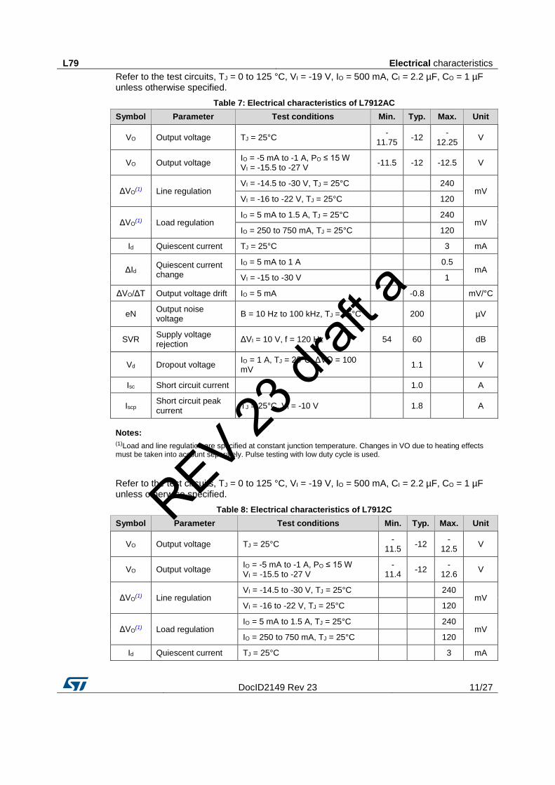
Table 7: Electrical characteristics of L7912AC
Symbol Parameter Test conditions Min. Typ. Max. Unit
VO Output voltage TJ = 25°C -
11.75 -12
-12.25
V
VO Output voltage IO = -5 mA to -1 A, PO ≤ 15 W VI = -15.5 to -27 V
-11.5 -12 -12.5 V
ΔVO(1) Line regulation
VI = -14.5 to -30 V, TJ = 25°C
240 mV
VI = -16 to -22 V, TJ = 25°C
120
ΔVO(1) Load regulation
IO = 5 mA to 1.5 A, TJ = 25°C
240 mV
IO = 250 to 750 mA, TJ = 25°C
120
Id Quiescent current TJ = 25°C
3 mA
ΔId Quiescent current change
IO = 5 mA to 1 A
0.5 mA
VI = -15 to -30 V
1
ΔVO/ΔT Output voltage drift IO = 5 mA
-0.8
mV/°C
eN Output noise voltage
B = 10 Hz to 100 kHz, TJ = 25°C
200
µV
SVR Supply voltage rejection
ΔVI = 10 V, f = 120 Hz 54 60
dB
Vd Dropout voltage IO = 1 A, TJ = 25°C, ΔVO = 100 mV
1.1
V
Isc Short circuit current
1.0
A
Iscp Short circuit peak current
TJ = 25°C, VI = -10 V
1.8
A
Notes:
(1)Load and line regulation are specified at constant junction temperature. Changes in VO due to heating effects must be taken into account separately. Pulse testing with low duty cycle is used.
Refer to the test circuits, TJ = 0 to 125 °C, VI = -19 V, IO = 500 mA, CI = 2.2 µF, CO = 1 µF unless otherwise specified.
Table 8: Electrical characteristics of L7912C
Symbol Parameter Test conditions Min. Typ. Max. Unit
VO Output voltage TJ = 25°C -
11.5 -12
-12.5
V
VO Output voltage IO = -5 mA to -1 A, PO ≤ 15 W VI = -15.5 to -27 V
-11.4
-12 -
12.6 V
ΔVO(1) Line regulation
VI = -14.5 to -30 V, TJ = 25°C
240 mV
VI = -16 to -22 V, TJ = 25°C
120
ΔVO(1) Load regulation
IO = 5 mA to 1.5 A, TJ = 25°C
240 mV
IO = 250 to 750 mA, TJ = 25°C
120
Id Quiescent current TJ = 25°C
3 mA
REV 23 dr
aft a
Electrical characteristics L79
12/27 DocID2149 Rev 23
Symbol Parameter Test conditions Min. Typ. Max. Unit
ΔId Quiescent current change
IO = 5 mA to 1 A
0.5 mA
VI = -15 to -30 V
1
ΔVO/ΔT Output voltage drift IO = 5 mA
-0.8
mV/°C
eN Output noise voltage
B = 10 Hz to 100 kHz, TJ = 25°C
200
µV
SVR Supply voltage rejection
ΔVI = 10 V, f = 120Hz 54 60
dB
Vd Dropout voltage IO = 1 A, TJ = 25°C, ΔVO = 100 mV
1.1
V
Isc Short circuit current
1.0
A
Notes:
(1)Load and line regulation are specified at constant junction temperature. Changes in VO due to heating effects must be taken into account separately. Pulse testing with low duty cycle is used.
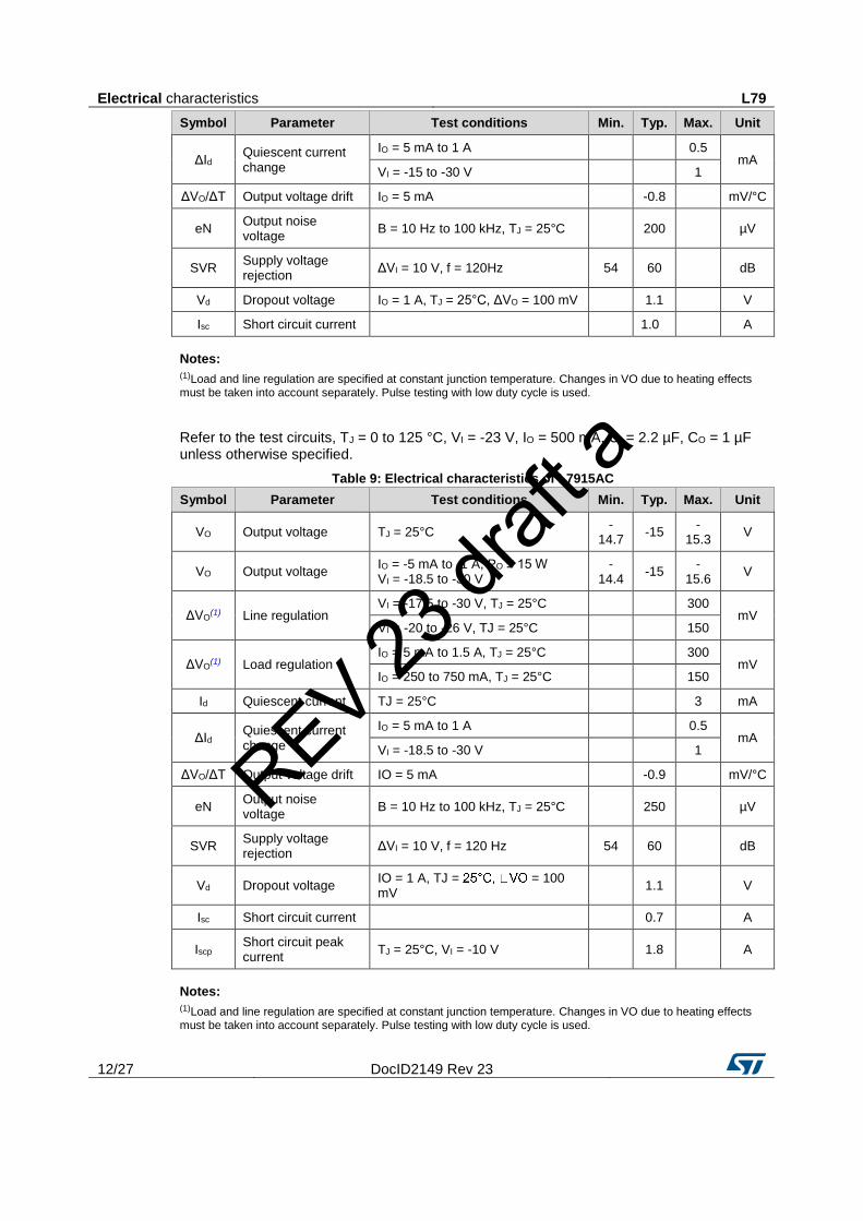
Refer to the test circuits, TJ = 0 to 125 °C, VI = -23 V, IO = 500 mA, CI = 2.2 µF, CO = 1 µF unless otherwise specified.
Table 9: Electrical characteristics of L7915AC
Symbol Parameter Test conditions Min. Typ. Max. Unit
VO Output voltage TJ = 25°C -
14.7 -15
-15.3
V
VO Output voltage IO = -5 mA to -1 A, PO ≤ 15 W VI = -18.5 to -30 V
-14.4
-15 -
15.6 V
ΔVO(1) Line regulation
VI = -17.5 to -30 V, TJ = 25°C
300 mV
VI = -20 to -26 V, TJ = 25°C
150
ΔVO(1) Load regulation
IO = 5 mA to 1.5 A, TJ = 25°C
300 mV
IO = 250 to 750 mA, TJ = 25°C
150
Id Quiescent current TJ = 25°C
3 mA
ΔId Quiescent current change
IO = 5 mA to 1 A
0.5 mA
VI = -18.5 to -30 V
1
ΔVO/ΔT Output voltage drift IO = 5 mA
-0.9
mV/°C
eN Output noise voltage
B = 10 Hz to 100 kHz, TJ = 25°C
250
µV
SVR Supply voltage rejection
ΔVI = 10 V, f = 120 Hz 54 60
dB
Vd Dropout voltage IO = 1 A, TJ = = 100 mV
1.1
V
Isc Short circuit current
0.7
A
Iscp Short circuit peak current
TJ = 25°C, VI = -10 V
1.8
A
Notes:
(1)Load and line regulation are specified at constant junction temperature. Changes in VO due to heating effects must be taken into account separately. Pulse testing with low duty cycle is used.
REV 23 dr
aft a
L79 Electrical characteristics
DocID2149 Rev 23 13/27
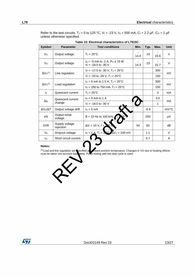
Refer to the test circuits, TJ = 0 to 125 °C, VI = -23 V, IO = 500 mA, CI = 2.2 µF, CO = 1 µF unless otherwise specified.
Table 10: Electrical characteristics of L7915C
Symbol Parameter Test conditions Min. Typ. Max. Unit
VO Output voltage TJ = 25°C -
14.4 -15
-15.6
V
VO Output voltage IO = -5 mA to -1 A, PO ≤ 15 W VI = -18.5 to -30 V
-14.3
-15 -
15.7 V
ΔVO(1) Line regulation
VI = -17.5 to -30 V, TJ = 25°C
300 mV
VI = -20 to -26 V, TJ = 25°C
150
ΔVO(1) Load regulation
IO = 5 mA to 1.5 A, TJ = 25°C
300 mV
IO = 250 to 750 mA, TJ = 25°C
150
Id Quiescent current TJ = 25°C
3 mA
ΔId Quiescent current change
IO = 5 mA to 1 A
0.5 mA
VI = -18.5 to -30 V
1
ΔVO/ΔT Output voltage drift IO = 5 mA
-0.9
mV/°C
eN Output noise voltage
B = 10 Hz to 100 kHz, TJ = 25°C
250
µV
SVR Supply voltage rejection
ΔVI = 10 V, f = 120 Hz 54 60
dB
Vd Dropout voltage IO = 1 A, TJ = 25°C, ΔVO = 100 mV
1.1
V
Isc Short circuit current
0.7
A
Notes:
(1)Load and line regulation are specified at constant junction temperature. Changes in VO due to heating effects must be taken into account separately. Pulse testing with low duty cycle is used.
REV 23 dr
aft a
Application information L79
14/27 DocID2149 Rev 23
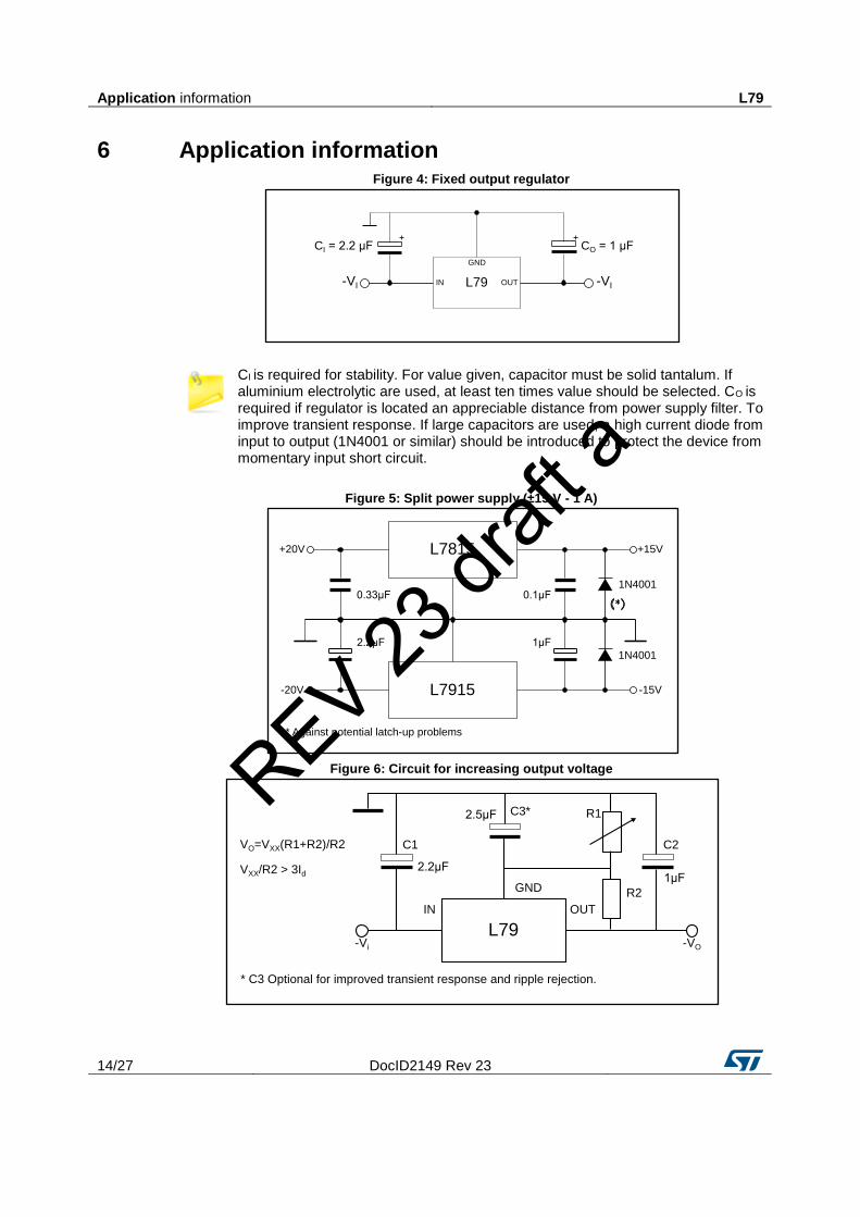
6 Application information Figure 4: Fixed output regulator
CI is required for stability. For value given, capacitor must be solid tantalum. If aluminium electrolytic are used, at least ten times value should be selected. CO is required if regulator is located an appreciable distance from power supply filter. To improve transient response. If large capacitors are used, a high current diode from input to output (1N4001 or similar) should be introduced to protect the device from momentary input short circuit.
Figure 5: Split power supply (±15 V - 1 A)
Figure 6: Circuit for increasing output voltage
-VI IN
GND
OUTL79
CO = 1 µFCI = 2.2 µF
-VI
1N4001
1N4001
L7815
L7915
* Against potential latch-up problems
-15V-20V
+20V +15V
0.33µF 0.1µF
1µF2.2µF
C3* R1
C2
1µF
-VO-Vi
L79
C1
IN
GND
OUT
2.2µF
2.5µF
R2
VO=VXX(R1+R2)/R2
VXX/R2 > 3Id
* C3 Optional for improved transient response and ripple rejection.
REV 23 dr
aft a
L79 Application information
DocID2149 Rev 23 15/27
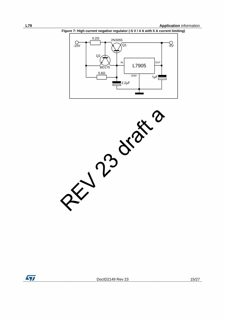
Figure 7: High current negative regulator (-5 V / 4 A with 5 A current limiting)
2N3055
BD175
IN OUT
GND
Q1
Q2
-10V -5V
L7905
0.2Ω
5.6Ω
2.2µF
1µF
REV 23 dr
aft a
Package information L79
16/27 DocID2149 Rev 23
7 Package information
In order to meet environmental requirements, ST offers these devices in different grades of ECOPACK® packages, depending on their level of environmental compliance. ECOPACK® specifications, grade definitions and product status are available at: www.st.com.
ECOPACK® is an ST trademark.
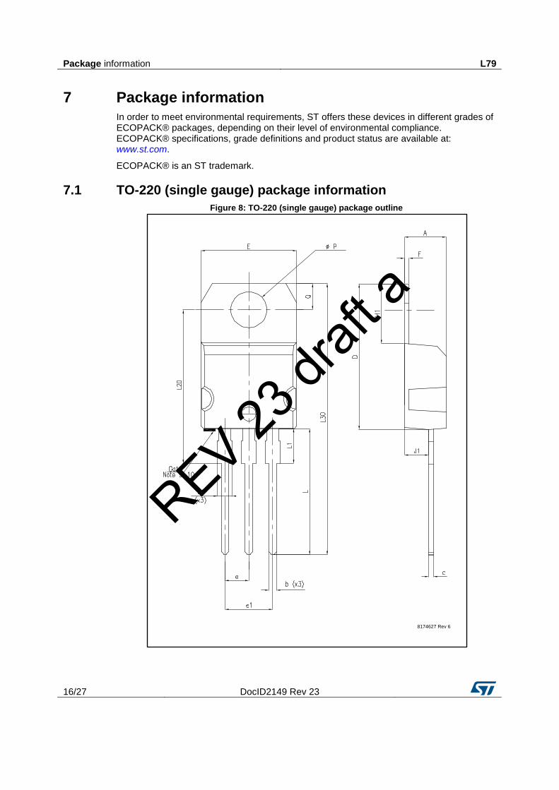
7.1 TO-220 (single gauge) package information
Figure 8: TO-220 (single gauge) package outline
8174627 Rev 6
REV 23 dr
aft a

L79 Package information
DocID2149 Rev 23 17/27
Table 11: TO-220 (single gauge) package mechanical data
Dim. mm
Min. Typ. Max.
A 4.40
4.60
b 0.61
0.88
b1 1.14
1.70
c 0.48
0.70
D 15.25
15.75
E 10.00
10.40
e 2.40
2.70
e1 4.95
5.15
F 0.51
0.60
H1 6.20
6.60
J1 2.40
2.72
L 13.00
14.00
L1 3.50
3.93
L20
16.40
L30
28.90
ΦP 3.75
3.85
Q 2.65
2.95
REV 23 dr
aft a
Package information L79
18/27 DocID2149 Rev 23
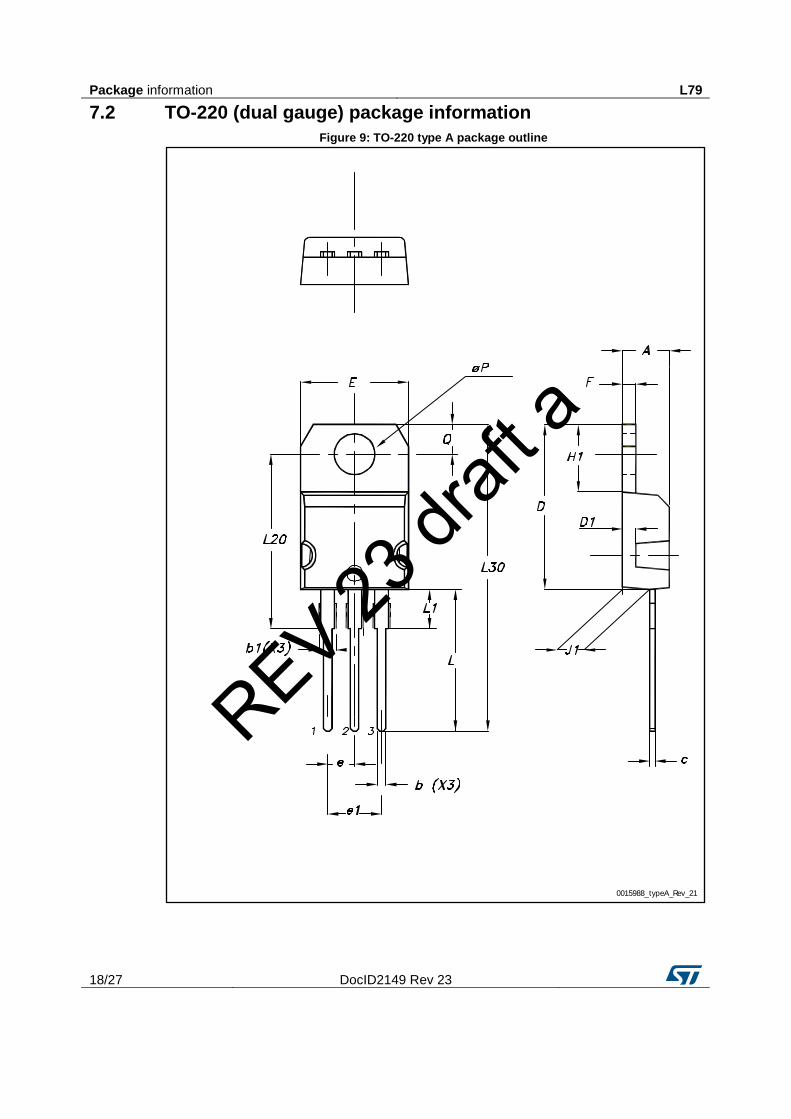
7.2 TO-220 (dual gauge) package information
Figure 9: TO-220 type A package outline
0015988_typeA_Rev_21
REV 23 dr
aft a
L79 Package information
DocID2149 Rev 23 19/27
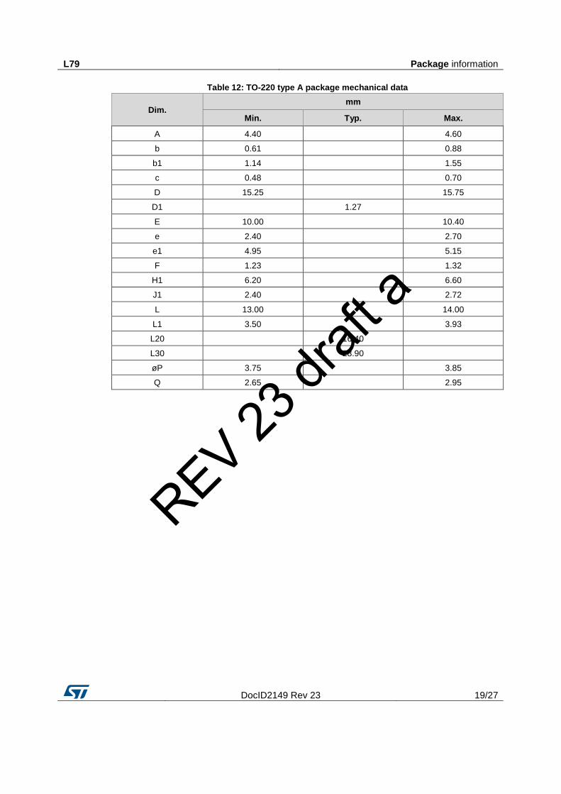
Table 12: TO-220 type A package mechanical data
Dim. mm
Min. Typ. Max.
A 4.40
4.60
b 0.61
0.88
b1 1.14
1.55
c 0.48
0.70
D 15.25
15.75
D1
1.27
E 10.00
10.40
e 2.40
2.70
e1 4.95
5.15
F 1.23
1.32
H1 6.20
6.60
J1 2.40
2.72
L 13.00
14.00
L1 3.50
3.93
L20
16.40
L30
28.90
øP 3.75
3.85
Q 2.65
2.95
REV 23 dr
aft a
Package information L79
20/27 DocID2149 Rev 23
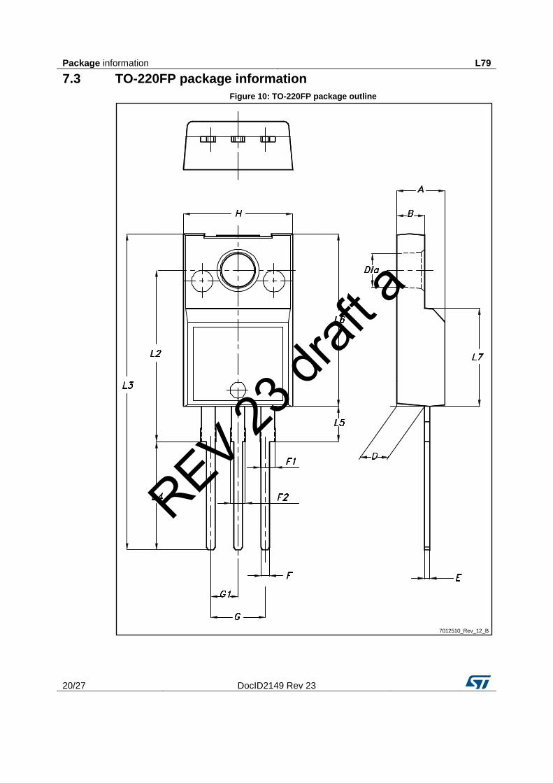
7.3 TO-220FP package information
Figure 10: TO-220FP package outline
7012510_Rev_12_B
REV 23 dr
aft a

L79 Package information
DocID2149 Rev 23 21/27
Table 13: TO-220FP package mechanical data
Dim. mm
Min. Typ. Max.
A 4.4
4.6
B 2.5
2.7
D 2.5
2.75
E 0.45
0.7
F 0.75
1
F1 1.15
1.70
F2 1.15
1.70
G 4.95
5.2
G1 2.4
2.7
H 10
10.4
L2
16
L3 28.6
30.6
L4 9.8
10.6
L5 2.9
3.6
L6 15.9
16.4
L7 9
9.3
Dia 3
3.2
REV 23 dr
aft a
Package information L79
22/27 DocID2149 Rev 23
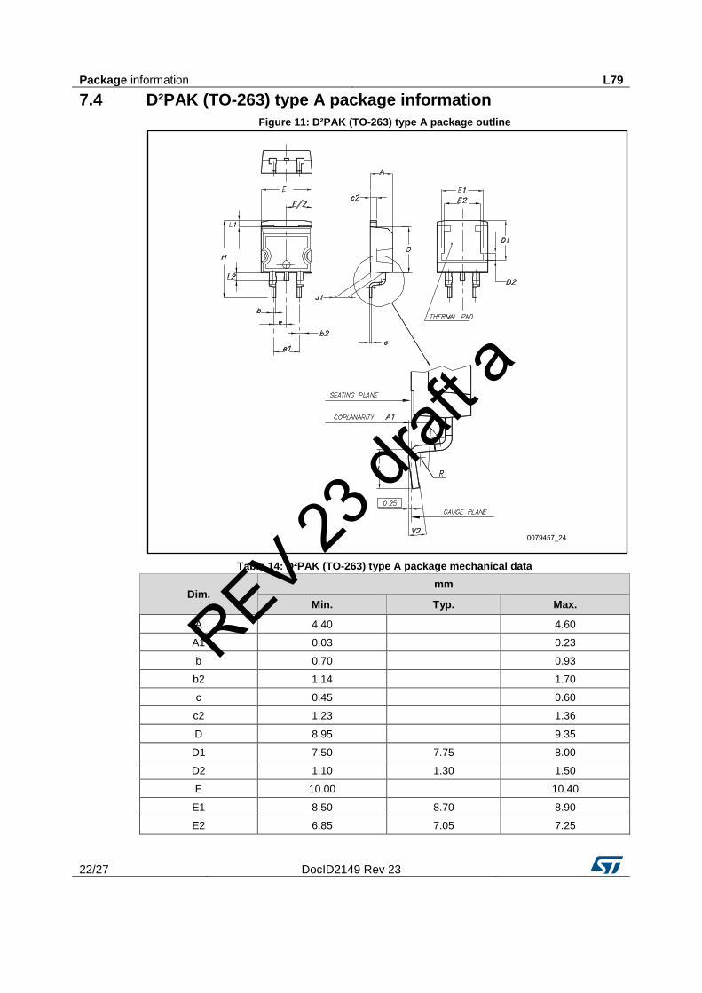
7.4 D²PAK (TO-263) type A package information
Figure 11: D²PAK (TO-263) type A package outline
Table 14: D²PAK (TO-263) type A package mechanical data
Dim. mm
Min. Typ. Max.
A 4.40
4.60
A1 0.03
0.23
b 0.70
0.93
b2 1.14
1.70
c 0.45
0.60
c2 1.23
1.36
D 8.95
9.35
D1 7.50 7.75 8.00
D2 1.10 1.30 1.50
E 10.00
10.40
E1 8.50 8.70 8.90
E2 6.85 7.05 7.25
REV 23 dr
aft a

L79 Package information
DocID2149 Rev 23 23/27
Dim. mm
Min. Typ. Max.
e
2.54
e1 4.88
5.28
H 15.00
15.85
J1 2.49
2.69
L 2.29
2.79
L1 1.27
1.40
L2 1.30
1.75
R
0.40
V2 0°
8°
Figure 12: D²PAK (TO-263) type A recommended footprint (dimensions are in mm)
Footprint
REV 23 dr
aft a
Package information L79
24/27 DocID2149 Rev 23
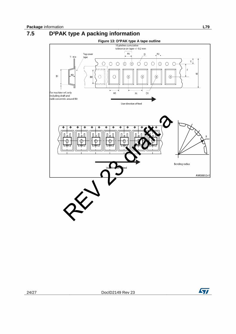
7.5 D²PAK type A packing information
Figure 13: D²PAK type A tape outline
REV 23 dr
aft a
L79 Package information
DocID2149 Rev 23 25/27
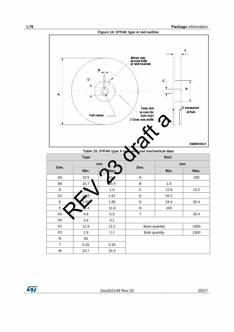
Figure 14: D²PAK type A reel outline
Table 15: D²PAK type A tape and reel mechanical data
Tape Reel
Dim. mm
Dim. mm
Min. Max. Min. Max.
A0 10.5 10.7 A
330
B0 15.7 15.9 B 1.5
D 1.5 1.6 C 12.8 13.2
D1 1.59 1.61 D 20.2
E 1.65 1.85 G 24.4 26.4
F 11.4 11.6 N 100
K0 4.8 5.0 T
30.4
P0 3.9 4.1
P1 11.9 12.1 Base quantity 1000
P2 1.9 2.1 Bulk quantity 1000
R 50
T 0.25 0.35
W 23.7 24.3
REV 23 dr
aft a
Revision history L79
26/27 DocID2149 Rev 23
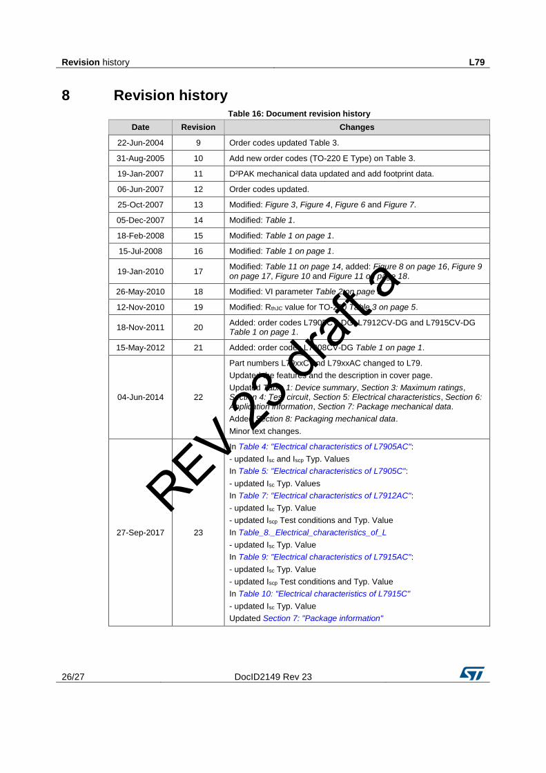
8 Revision history Table 16: Document revision history
Date Revision Changes
22-Jun-2004 9 Order codes updated Table 3.
31-Aug-2005 10 Add new order codes (TO-220 E Type) on Table 3.
19-Jan-2007 11 D²PAK mechanical data updated and add footprint data.
06-Jun-2007 12 Order codes updated.
25-Oct-2007 13 Modified: Figure 3, Figure 4, Figure 6 and Figure 7.
05-Dec-2007 14 Modified: Table 1.
18-Feb-2008 15 Modified: Table 1 on page 1.
15-Jul-2008 16 Modified: Table 1 on page 1.
19-Jan-2010 17 Modified: Table 11 on page 14, added: Figure 8 on page 16, Figure 9 on page 17, Figure 10 and Figure 11 on page 18.
26-May-2010 18 Modified: VI parameter Table 2 on page 5.
12-Nov-2010 19 Modified: RthJC value for TO-220 Table 3 on page 5.
18-Nov-2011 20 Added: order codes L7905CV-DG, L7912CV-DG and L7915CV-DG Table 1 on page 1.
15-May-2012 21 Added: order codes L7908CV-DG Table 1 on page 1.
04-Jun-2014 22
Part numbers L79xxC and L79xxAC changed to L79.
Updated the features and the description in cover page.
Updated Table 1: Device summary, Section 3: Maximum ratings, Section 4: Test circuit, Section 5: Electrical characteristics, Section 6: Application information, Section 7: Package mechanical data.
Added Section 8: Packaging mechanical data.
Minor text changes.
27-Sep-2017 23
In Table 4: "Electrical characteristics of L7905AC":
- updated Isc and Iscp Typ. Values
In Table 5: "Electrical characteristics of L7905C":
- updated Isc Typ. Values
In Table 7: "Electrical characteristics of L7912AC":
- updated Isc Typ. Value
- updated Iscp Test conditions and Typ. Value
In Table_8._Electrical_characteristics_of_L
- updated Isc Typ. Value
In Table 9: "Electrical characteristics of L7915AC":
- updated Isc Typ. Value
- updated Iscp Test conditions and Typ. Value
In Table 10: "Electrical characteristics of L7915C"
- updated Isc Typ. Value
Updated Section 7: "Package information"
REV 23 dr
aft a
L79
DocID2149 Rev 23 27/27
IMPORTANT NOTICE – PLEASE READ CAREFULLY
STMicroelectronics NV and its subsidiaries (“ST”) reserve the right to make changes, corrections, enhancements, modifications , and improvements to ST products and/or to this document at any time without notice. Purchasers should obtain the latest relevant information on ST products before placing orders. ST products are sold pursuant to ST’s terms and conditions of sale in place at the time of order acknowledgement.
Purchasers are solely responsible for the choice, selection, and use of ST products and ST assumes no liability for application assistance or the design of Purchasers’ products.
No license, express or implied, to any intellectual property right is granted by ST herein.
Resale of ST products with provisions different from the information set forth herein shall void any warranty granted by ST for such product.
ST and the ST logo are trademarks of ST. All other product or service names are the property of their respective owners.
Information in this document supersedes and replaces information previously supplied in any prior versions of this document.
© 2017 STMicroelectronics – All rights reserved
REV 23 dr
aft a