Embed Size (px)
Citation preview
ECE Laboratory Exercise 3Introduction to myDAQ Variable Analog Signals and Voltage Dividers
ECE 109 Laboratory Exercise 3
Introduction to myDAQ Variable Analog Signals and Voltage Dividers
OBJECTIVES
Gain experience in designing a voltage divider circuit Gain experience in analyzing a voltage divider circuit Gain experience in analyzing the effects source variation and load variation referred to
as Source Regulation and Load Regulation (Burden) of a voltage divider circuit
EQUIPMENT REQUIRED
Protoboard---- students must provide their own. Contact SCETA 9-257 for availability. Two banana cables---- students must supply their own. One lot of clip leads---- students must supply their own clip leads. National Instruments myDAQ---- supplied by ECE Department. One lot of resistors ----available in the 5th floor stock/supply lab. The ratio of the smallest
resistor to the largest should be less than 5 is suggested. You will need about 7 resistors. Keep them for future labs.
One lot of small solid wires---- AWG 20 through 24 (insulated solid wire not stranded) for connecting to the myDAQ terminals and protoboards.
PROCEDURE
Create a dc variable output voltage from the myDAQ analog output terminals A00 or A01 and create analog input terminals (AI 0+ and AI0-) to verify that the output voltage is operating properly. You could just connect a dc voltmeter to the output terminals but then you wouldn’t be taking advantage of the built-in myDAQ meters. Verify the output voltage using the myDAQ voltmeter. Demonstrate the VI to your instructor. What is the percent difference between the VI control panel voltmeter and the myDAQ voltmeter? % difference_________________.
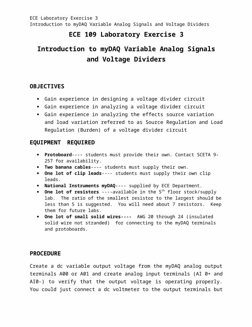
1. Open LabVIEW and a new virtual instrument (V), see Figure3-1.
ECE Laboratory Exercise 3Introduction to myDAQ Variable Analog Signals and Voltage Dividers
Figure 3-1. Creating a new Virtual Instrument.
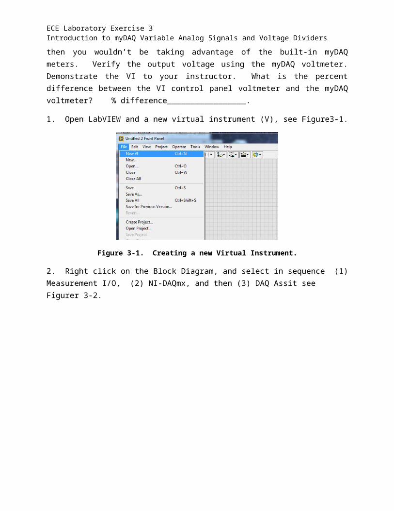
2. Right click on the Block Diagram, and select in sequence (1) Measurement I/O, (2) NI-DAQmx, and then (3) DAQ Assit see Figurer 3-2.
Figure 3-2. Selecting DAQ Assist
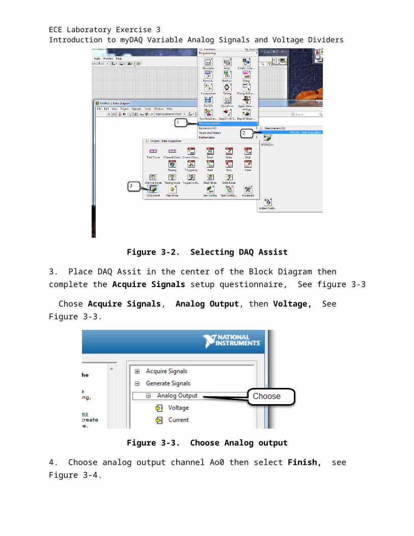
3. Place DAQ Assit in the center of the Block Diagram then complete the Acquire Signals setup questionnaire, See figure 3-3
Chose Acquire Signals, Analog Output, then Voltage, See Figure 3-3.
ECE Laboratory Exercise 3Introduction to myDAQ Variable Analog Signals and Voltage Dividers
Figure 3-3. Choose Analog output
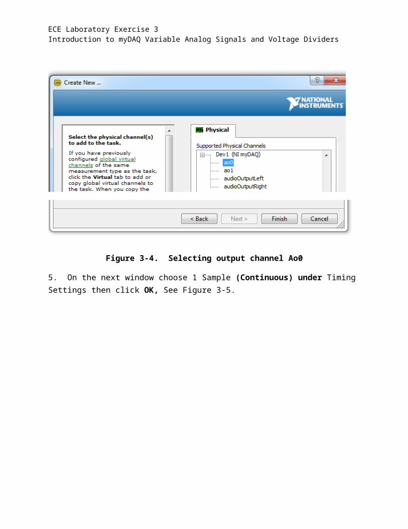
4. Choose analog output channel Ao0 then select Finish, see Figure 3-4.
Figure 3-4. Selecting output channel Ao0
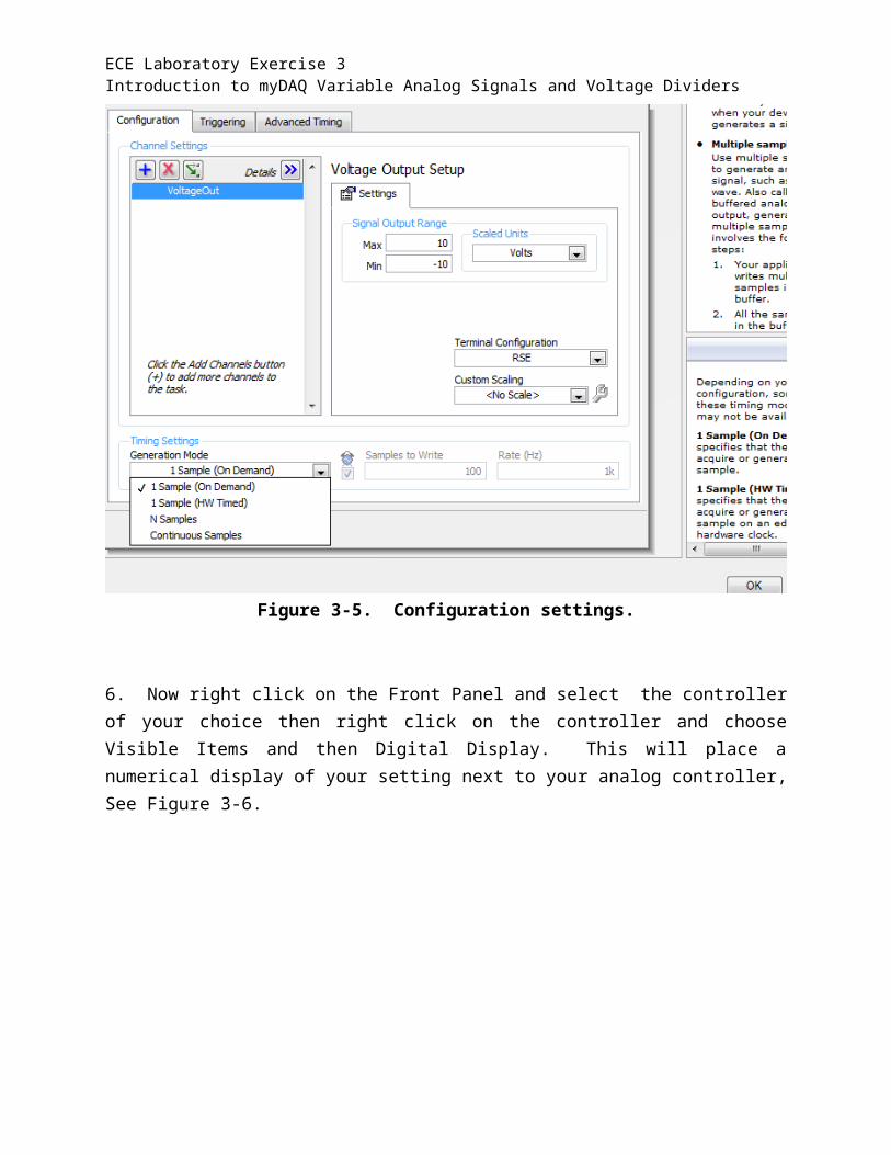
5. On the next window choose 1 Sample (Continuous) under Timing Settings then click OK, See Figure 3-5.
ECE Laboratory Exercise 3Introduction to myDAQ Variable Analog Signals and Voltage Dividers
Figure 3-5. Configuration settings.
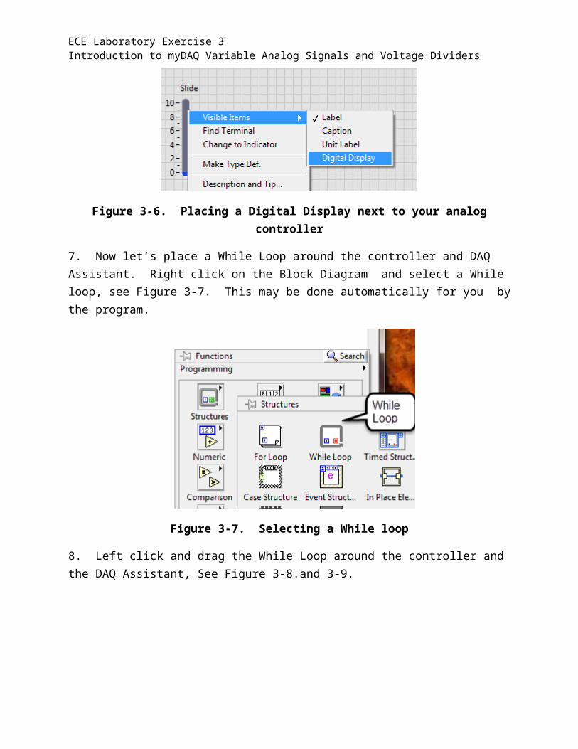
6. Now right click on the Front Panel and select the controller of your choice then right click on the controller and choose Visible Items and then Digital Display. This will place a numerical display of your setting next to your analog controller, See Figure 3-6.
Figure 3-6. Placing a Digital Display next to your analog controller
ECE Laboratory Exercise 3Introduction to myDAQ Variable Analog Signals and Voltage Dividers
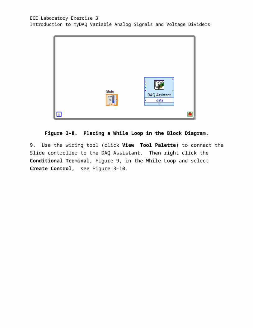
7. Now let’s place a While Loop around the controller and DAQ Assistant. Right click on the Block Diagram and select a While loop, see Figure 3-7. This may be done automatically for you by the program.
Figure 3-7. Selecting a While loop
8. Left click and drag the While Loop around the controller and the DAQ Assistant, See Figure 3-8.and 3-9.
Figure 3-8. Placing a While Loop in the Block Diagram.
ECE Laboratory Exercise 3Introduction to myDAQ Variable Analog Signals and Voltage Dividers
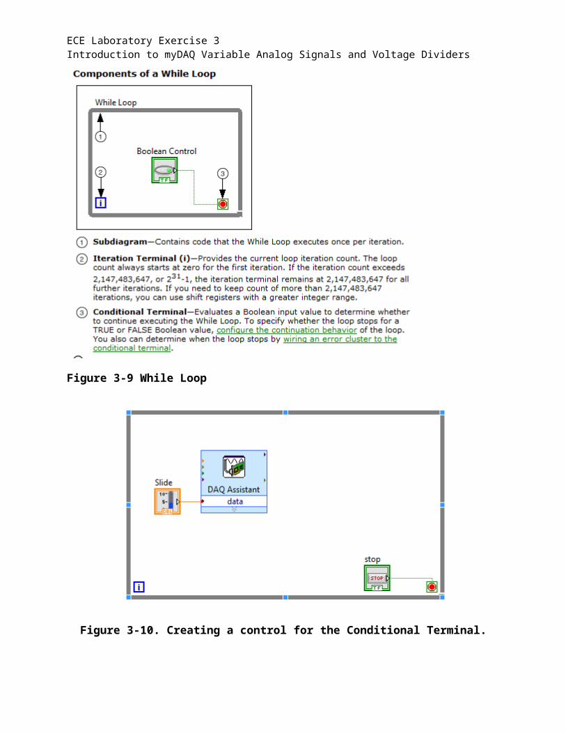
9. Use the wiring tool (click View Tool Palette) to connect the Slide controller to the DAQ Assistant. Then right click the Conditional Terminal, Figure 9, in the While Loop and select Create Control, see Figure 3-10.
Figure 3-9 While Loop
ECE Laboratory Exercise 3Introduction to myDAQ Variable Analog Signals and Voltage Dividers
Figure 3-10. Creating a control for the Conditional Terminal.
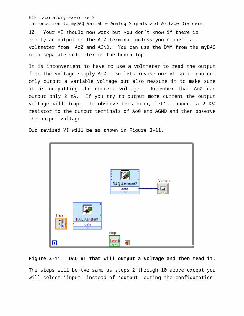
10. Your VI should now work but you don’t know if there is really an output on the Ao0 terminal unless you connect a voltmeter from Ao0 and AGND. You can use the DMM from the myDAQ or a separate voltmeter on the bench top.
It is inconvenient to have to use a voltmeter to read the output from the voltage supply Ao0. So lets revise our VI so it can not only output a variable voltage but also measure it to make sure it is outputting the correct voltage. Remember that Ao0 can output only 2 mA. If you try to output more current the output voltage will drop. To observe this drop, let’s connect a 2 K resistor to the output terminals of Ao0 and AGND and then observe the output voltage.
Our revised VI will be as shown in Figure 3-11.
ECE Laboratory Exercise 3Introduction to myDAQ Variable Analog Signals and Voltage Dividers
Figure 3-11. DAQ VI that will output a voltage and then read it.
The steps will be the same as steps 2 through 10 above except you will select “input” instead of “output” during the configuration process. The display will be a Numeric Indicator rather than a numeric controller.
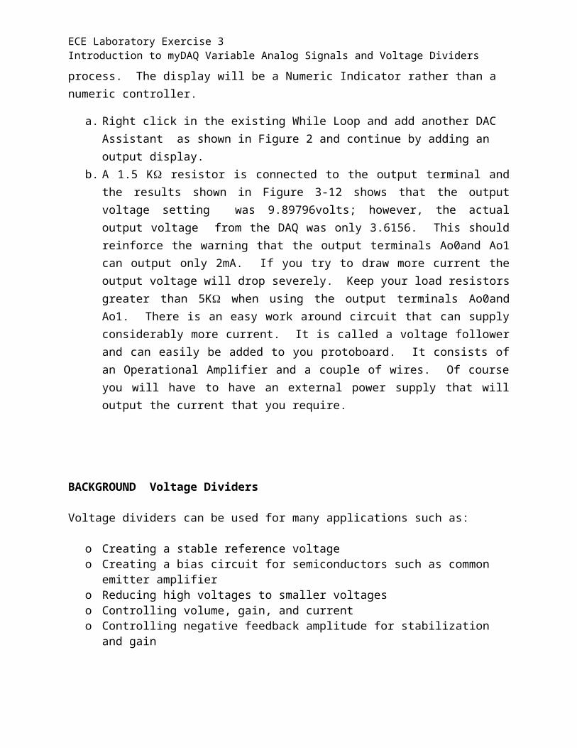
a. Right click in the existing While Loop and add another DAC Assistant as shown in Figure 2 and continue by adding an output display.
b. A 1.5 K resistor is connected to the output terminal and the results shown in Figure 3-12 shows that the output voltage setting was 9.89796volts; however, the actual output voltage from the DAQ was only 3.6156. This should reinforce the warning that the output terminals Ao0and Ao1 can output only 2mA. If you try to draw more current the output voltage will drop severely. Keep your load resistors greater than 5K when using the output terminals Ao0and Ao1. There is an easy work around circuit that can supply considerably more current. It is called a voltage follower and can easily be added to you protoboard. It consists of an Operational Amplifier and a couple of wires. Of course you will have to have an external power supply that will output the current that you require.
ECE Laboratory Exercise 3Introduction to myDAQ Variable Analog Signals and Voltage Dividers
BACKGROUND Voltage Dividers
Voltage dividers can be used for many applications such as:
o Creating a stable reference voltageo Creating a bias circuit for semiconductors such as common emitter amplifiero Reducing high voltages to smaller voltageso Controlling volume, gain, and current o Controlling negative feedback amplitude for stabilization and gain
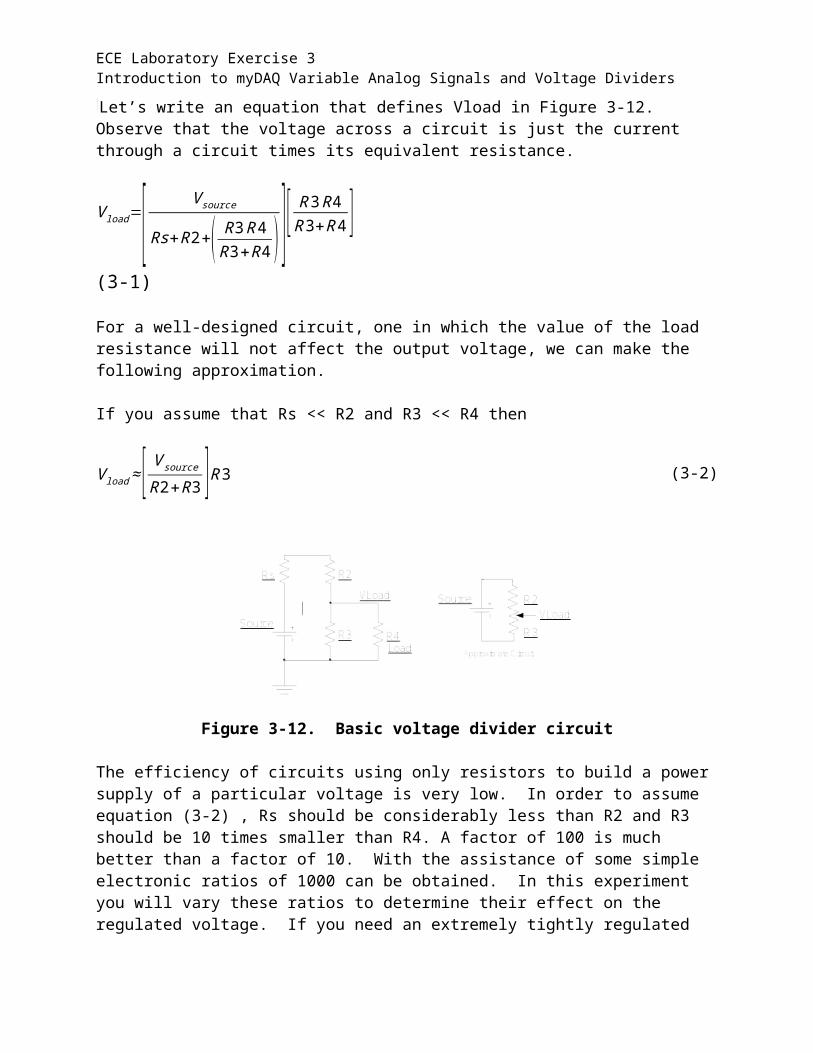
Let’s write an equation that defines Vload in Figure 3-12. Observe that the voltage across a circuit is just the current through a circuit times its equivalent resistance.
V load=[ V source
Rs+R2+( R3 R 4R3+R4 ) ][ R3R 4R3+R 4 ] (3-1)
For a well-designed circuit, one in which the value of the load resistance will not affect the output voltage, we can make the following approximation.
If you assume that Rs << R2 and R3 << R4 then
V load≈ [ V sourceR2+R3 ]R3 (3-2)
Figure 3-12. Basic voltage divider circuit
The efficiency of circuits using only resistors to build a power supply of a particular voltage is very low. In order to assume equation (3-2) , Rs should be considerably less than R2 and R3 should be 10 times smaller than R4. A factor of 100 is much better than a factor of 10. With the assistance of some simple electronic ratios of 1000 can be obtained. In this experiment you will vary these ratios to determine their effect on the regulated voltage. If you need an extremely
ECE Laboratory Exercise 3Introduction to myDAQ Variable Analog Signals and Voltage Dividers
tightly regulated voltage, then you will have to use an electronic regulated supply which is not covered in this course.
As a designer you will need to find the voltage regulation of your circuit. Voltage regulation expressed in percent is defined as the variation in the load voltage as the load changes. See equation 3-3. A smaller number is better regulation.
Voltage Regulation(% )=Vout no load−Vout full load
Voutno load*100 (3-3)
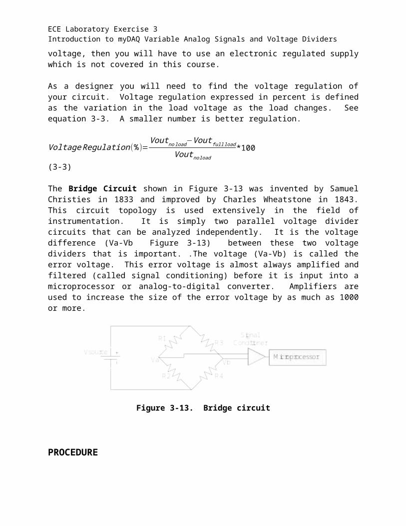
The Bridge Circuit shown in Figure 3-13 was invented by Samuel Christies in 1833 and improved by Charles Wheatstone in 1843. This circuit topology is used extensively in the field of instrumentation. It is simply two parallel voltage divider circuits that can be analyzed independently. It is the voltage difference (Va-Vb Figure 3-13) between these two voltage dividers that is important. .The voltage (Va-Vb) is called the error voltage. This error voltage is almost always amplified and filtered (called signal conditioning) before it is input into a microprocessor or analog-to-digital converter. Amplifiers are used to increase the size of the error voltage by as much as 1000 or more.
Figure 3-13. Bridge circuit
PROCEDURE
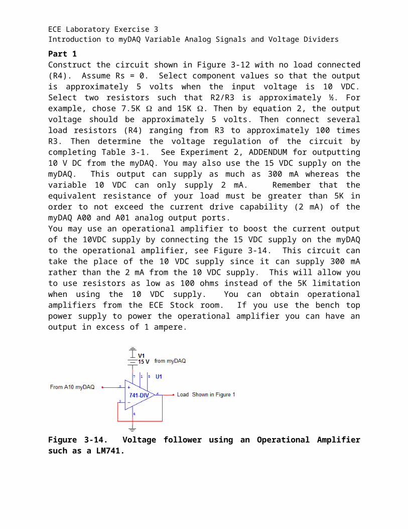
Part 1Construct the circuit shown in Figure 3-12 with no load connected (R4). Assume Rs = 0. Select component values so that the output is approximately 5 volts when the input voltage is 10 VDC. Select two resistors such that R2/R3 is approximately ½. For example, chose 7.5K and 15K . Then by equation 2, the output voltage should be approximately 5 volts. Then connect several load resistors (R4) ranging from R3 to approximately 100 times R3. Then determine the voltage regulation of the circuit by completing Table 3-1. See Experiment 2, ADDENDUM for outputting 10 V DC from the myDAQ. You may also use the 15 VDC supply on the myDAQ. This output can supply as much as 300 mA whereas the variable 10 VDC can only supply 2 mA. Remember that
ECE Laboratory Exercise 3Introduction to myDAQ Variable Analog Signals and Voltage Dividers
the equivalent resistance of your load must be greater than 5K in order to not exceed the current drive capability (2 mA) of the myDAQ A00 and A01 analog output ports. You may use an operational amplifier to boost the current output of the 10VDC supply by connecting the 15 VDC supply on the myDAQ to the operational amplifier, see Figure 3-14. This circuit can take the place of the 10 VDC supply since it can supply 300 mA rather than the 2 mA from the 10 VDC supply. This will allow you to use resistors as low as 100 ohms instead of the 5K limitation when using the 10 VDC supply. You can obtain operational amplifiers from the ECE Stock room. If you use the bench top power supply to power the operational amplifier you can have an output in excess of 1 ampere.
Figure 3-14. Voltage follower using an Operational Amplifier such as a LM741.
Table 3-1. Voltage Regulator AnalysisVS
DMM
R2
DMM
R3
DMM
R4 (Load)
Approx. values
Vout
DMM
Regulation %
Eq. (3)
5K
15K
150K
1 M
0
ECE Laboratory Exercise 3Introduction to myDAQ Variable Analog Signals and Voltage Dividers
Part 2.Construct the bridge circuit shown in Figure 2. Choose resistors R2, R3, and R4 with the same value. R1 will be used to simulate a sensor. Choose R1 to be a value close to R2 but LESS than R2. All resistor values should be greater than 5K.
Calculate the voltage Va, Vb, and Va-Vb using equation 4. The error voltage of the bridge is Va-Vb. It is usually input into an amplifier that increases its value before it is input into a microprocessor such as an Arduino or PIC. Note that the error voltage (Va-Vb) is directly proportional to the source voltage. If you increase the source voltage to high then self-heating of the resistors which is proportional to the square of the source voltage will cause errors. Use an input voltage of something between 1 and 10 VDC..
error voltage=(Va−Vb)=Vs ( R2R1+R1
−12 ) (3-4)
Enter your resistor values into Table 3-2 then complete the table. Choose two different values for R1. Calculate the required amplifier gain so that the output of the amplifier is 5 volts using equation 3-5. Note that the gain increases the closer R1 is to R2, R3, and R4 because the error voltage decreases.
Gain=V out
error voltage= VoutVa−Vb
= 5Va−Vb
(3-5)
Table 3-2. Bridge circuit analysis data using the myDAQ and DMMResistor Va Vb Va-Vb Amplifier Gain
R1=
R1 =
R2=R3=R4=
Vs=
ECE Laboratory Exercise 3Introduction to myDAQ Variable Analog Signals and Voltage Dividers
Your laboratory report is due in one week (the next lab class).


![Shadowrun: Street Grimoire, 2nd Printing · HEALTH SPELLS 109 Ambidexterity 109 Alleviate Addiction 109 Alleviate [Allergy] 109 Awaken 109 ... Advanced Alchemy/ Ritual/Spellcasting](https://img.pdfslide.net/doc/110x75/5f0367d57e708231d4090d07/shadowrun-street-grimoire-2nd-printing-health-spells-109-ambidexterity-109-alleviate.jpg)


![MEMS based voltage references - VTT...3 Kärkkäinen, Anna-Maija. MEMS based voltage references [MEMSiin perustuvat jännite-referenssit]. Espoo 2006. VTT Publications 613. 109 p](https://img.pdfslide.net/doc/110x75/603039e3b05741304b5bc635/mems-based-voltage-references-vtt-3-krkkinen-anna-maija-mems-based-voltage.jpg)