Embed Size (px)
Citation preview
S-13A1 Series
www.ablicinc.com
HIGH RIPPLE-REJECTION LOW DROPOUTHIGH OUTPUT CURRENT CMOS VOLTAGE REGULATOR
© ABLIC Inc., 2011-2016 Rev.2.1_01
1
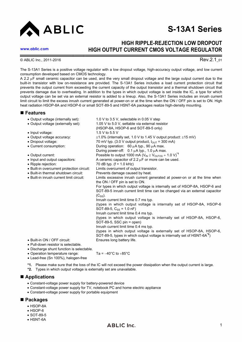
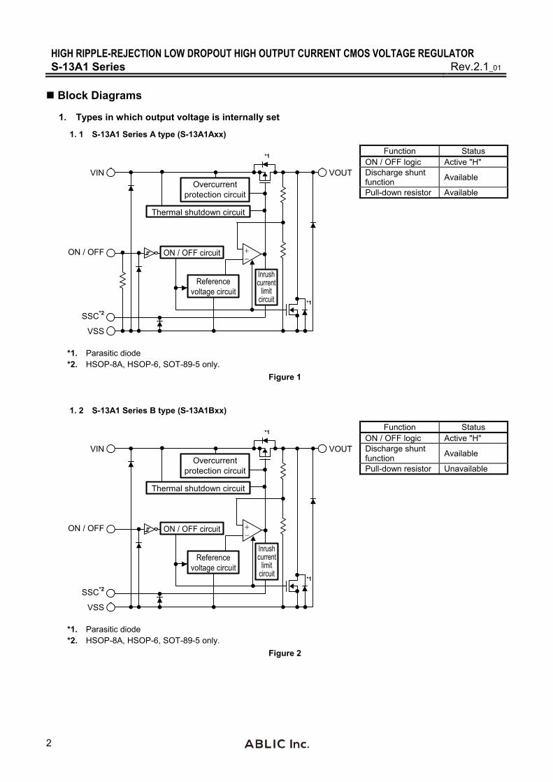
The S-13A1 Series is a positive voltage regulator with a low dropout voltage, high-accuracy output voltage, and low current consumption developed based on CMOS technology. A 2.2 F small ceramic capacitor can be used, and the very small dropout voltage and the large output current due to the built-in transistor with low on-resistance are provided. The S-13A1 Series includes a load current protection circuit that prevents the output current from exceeding the current capacity of the output transistor and a thermal shutdown circuit that prevents damage due to overheating. In addition to the types in which output voltage is set inside the IC, a type for which output voltage can be set via an external resistor is added to a lineup. Also, the S-13A1 Series includes an inrush current limit circuit to limit the excess inrush current generated at power-on or at the time when the ON / OFF pin is set to ON. High heat radiation HSOP-8A and HSOP-6 or small SOT-89-5 and HSNT-6A packages realize high-density mounting.
Features
Output voltage (internally set): 1.0 V to 3.5 V, selectable in 0.05 V step Output voltage (externally set): 1.05 V to 5.0 V, settable via external resistor (HSOP-8A, HSOP-6 and SOT-89-5 only) Input voltage: 1.5 V to 5.5 V Output voltage accuracy: 1.0% (internally set, 1.0 V to 1.45 V output product: 15 mV) Dropout voltage: 70 mV typ. (3.0 V output product, IOUT = 300 mA) Current consumption: During operation: 60 A typ., 90 A max.
During power-off: 0.1 A typ., 1.0 A max. Output current: Possible to output 1000 mA (VIN VOUT(S) 1.0 V)*1 Input and output capacitors: A ceramic capacitor of 2.2 F or more can be used. Ripple rejection: 70 dB typ. (f = 1.0 kHz) Built-in overcurrent protection circuit: Limits overcurrent of output transistor. Built-in thermal shutdown circuit: Prevents damage caused by heat. Built-in inrush current limit circuit: Limits excessive inrush current generated at power-on or at the time when
the ON / OFF pin is set to ON. For types in which output voltage is internally set of HSOP-8A, HSOP-6 and SOT-89-5 inrush current limit time can be changed via an external capacitor (CSS).
Inrush current limit time 0.7 ms typ. (types in which output voltage is internally set of HSOP-8A, HSOP-6
SOT-89-5, CSS = 1.0 nF) Inrush current limit time 0.4 ms typ. (types in which output voltage is internally set of HSOP-8A, HSOP-6,
SOT-89-5, SSC pin = open) Inrush current limit time 0.4 ms typ. (types in which output voltage is externally set of HSOP-8A, HSOP-6,
SOT-89-5, types in which output voltage is internally set of HSNT-6A*2) Built-in ON / OFF circuit: Ensures long battery life. Pull-down resistor is selectable. Discharge shunt function is selectable. Operation temperature range: Ta = 40°C to 85°C Lead-free (Sn 100%), halogen-free
*1. Please make sure that the loss of the IC will not exceed the power dissipation when the output current is large. *2. Types in which output voltage is externally set are unavailable.
Applications Constant-voltage power supply for battery-powered device Constant-voltage power supply for TV, notebook PC and home electric appliance Constant-voltage power supply for portable equipment
Packages HSOP-8A HSOP-6 SOT-89-5 HSNT-6A
www.ablic.com
HIGH RIPPLE-REJECTION LOW DROPOUT HIGH OUTPUT CURRENT CMOS VOLTAGE REGULATOR S-13A1 Series Rev.2.1_01
2
Block Diagrams
1. Types in which output voltage is internally set
1. 1 S-13A1 Series A type (S-13A1Axx)
VSS
ON / OFF
VIN VOUT
*1
ON / OFF circuit
Reference voltage circuit
Overcurrent protection circuit
Thermal shutdown circuit
Inrush current
limit circuit
SSC*2
*1
*1. Parasitic diode *2. HSOP-8A, HSOP-6, SOT-89-5 only.
Function Status ON / OFF logic Active "H" Discharge shunt function
Available
Pull-down resistor Available
Figure 1
1. 2 S-13A1 Series B type (S-13A1Bxx)
VSS
ON / OFF
VIN VOUT
*1
ON / OFF circuit
Reference voltage circuit
Overcurrent protection circuit
Thermal shutdown circuit
SSC*2
*1
Inrush current
limit circuit
*1. Parasitic diode *2. HSOP-8A, HSOP-6, SOT-89-5 only.
Function Status ON / OFF logic Active "H" Discharge shunt function
Available
Pull-down resistor Unavailable
Figure 2
HIGH RIPPLE-REJECTION LOW DROPOUT HIGH OUTPUT CURRENT CMOS VOLTAGE REGULATORRev.2.1_01 S-13A1 Series
3
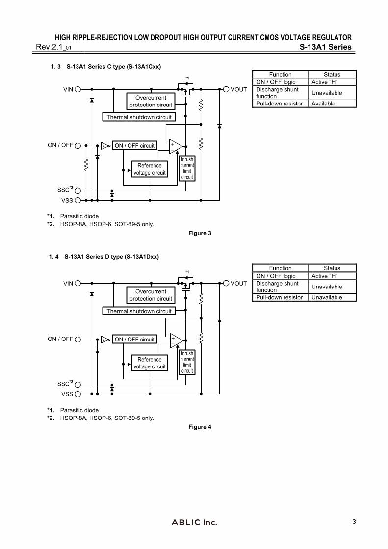
1. 3 S-13A1 Series C type (S-13A1Cxx)
VSS
ON / OFF
VIN VOUT
*1
ON / OFF circuit
Reference voltage circuit
Overcurrent protection circuit
Thermal shutdown circuit
SSC*2
Inrushcurrent
limit circuit
*1. Parasitic diode *2. HSOP-8A, HSOP-6, SOT-89-5 only.
Function Status ON / OFF logic Active "H" Discharge shunt function
Unavailable
Pull-down resistor Available
Figure 3
1. 4 S-13A1 Series D type (S-13A1Dxx)
VSS
ON / OFF
VIN VOUT
*1
ON / OFF circuit
Reference voltage circuit
Overcurrent protection circuit
Thermal shutdown circuit
SSC*2
Inrushcurrent
limit circuit
*1. Parasitic diode *2. HSOP-8A, HSOP-6, SOT-89-5 only.
Function Status ON / OFF logic Active "H" Discharge shunt function
Unavailable
Pull-down resistor Unavailable
Figure 4
HIGH RIPPLE-REJECTION LOW DROPOUT HIGH OUTPUT CURRENT CMOS VOLTAGE REGULATOR S-13A1 Series Rev.2.1_01
4
2. Types in which output voltage is externally set (HSOP-8A, HSOP-6 and SOT-89-5 only)
2. 1 S-13A1 Series A type (S-13A1A00)
VSS
ON / OFF
VIN VOUT
*1
VADJ
Overcurrent protection circuit
Thermal shutdown circuit
ON / OFF circuit
Reference voltage circuit
Inrushcurrent
limit circuit *1
*1. Parasitic diode
Function Status ON / OFF logic Active "H" Discharge shunt function
Available
Pull-down resistor Available
Figure 5
2. 2 S-13A1 Series B type (S-13A1B00)
VSS
ON / OFF
VIN VOUT
*1
VADJ
Overcurrent protection circuit
Thermal shutdown circuit
ON / OFF circuit
Reference voltage circuit
Inrushcurrent
limit circuit *1
*1. Parasitic diode
Function Status ON / OFF logic Active "H" Discharge shunt function
Available
Pull-down resistor Unavailable
Figure 6
HIGH RIPPLE-REJECTION LOW DROPOUT HIGH OUTPUT CURRENT CMOS VOLTAGE REGULATORRev.2.1_01 S-13A1 Series
5
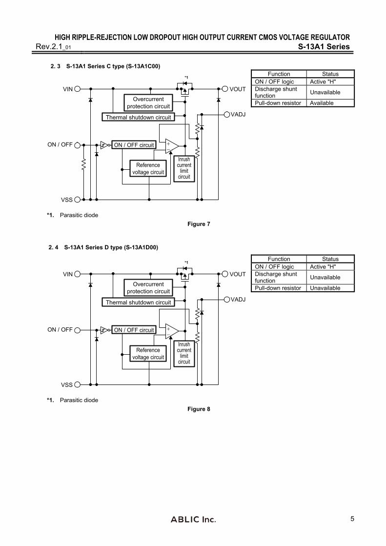
2. 3 S-13A1 Series C type (S-13A1C00)
VSS
ON / OFF
VIN VOUT
*1
VADJ
Overcurrent protection circuit
Thermal shutdown circuit
ON / OFF circuit
Reference voltage circuit
Inrushcurrent
limit circuit
*1. Parasitic diode
Function Status ON / OFF logic Active "H" Discharge shunt function
Unavailable
Pull-down resistor Available
Figure 7
2. 4 S-13A1 Series D type (S-13A1D00)
VSS
ON / OFF
VIN VOUT
*1
VADJ
Overcurrent protection circuit
Thermal shutdown circuit
ON / OFF circuit
Reference voltage circuit
Inrushcurrent
limit circuit
*1. Parasitic diode
Function Status ON / OFF logic Active "H" Discharge shunt function
Unavailable
Pull-down resistor Unavailable
Figure 8
HIGH RIPPLE-REJECTION LOW DROPOUT HIGH OUTPUT CURRENT CMOS VOLTAGE REGULATOR S-13A1 Series Rev.2.1_01
6
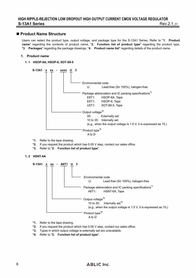
Product Name Structure
Users can select the product type, output voltage, and package type for the S-13A1 Series. Refer to "1. Product name" regarding the contents of product name, "2. Function list of product type" regarding the product type, "3. Packages" regarding the package drawings, "4. Product name list" regarding details of the product name.
1. Product name
1. 1 HSOP-8A, HSOP-6, SOT-89-5
S-13A1 x xx - xxxx U 3
Product type*3 A to D
Package abbreviation and IC packing specifications*1 E8T1: HSOP-8A, Tape E6T1: HSOP-6, Tape U5T1: SOT-89-5, Tape
Output voltage*2
00: Externally set 10 to 35: Internally set
(e.g., when the output voltage is 1.0 V, it is expressed as 10.)
Environmental code U: Lead-free (Sn 100%), halogen-free
*1. Refer to the tape drawing. *2. If you request the product which has 0.05 V step, contact our sales office. *3. Refer to "2. Function list of product type".
1. 2 HSNT-6A
S-13A1 x xx - A6T1 U 3
Product type*4 A to D
Package abbreviation and IC packing specifications*1 A6T1: HSNT-6A, Tape
Output voltage*2 10 to 35: Internally set*3 (e.g., when the output voltage is 1.0 V, it is expressed as 10.)
Environmental code U: Lead-free (Sn 100%), halogen-free
*1. Refer to the tape drawing. *2. If you request the product which has 0.05 V step, contact our sales office. *3. Types in which output voltage is externally set are unavailable. *4. Refer to "2. Function list of product type".
HIGH RIPPLE-REJECTION LOW DROPOUT HIGH OUTPUT CURRENT CMOS VOLTAGE REGULATORRev.2.1_01 S-13A1 Series
7
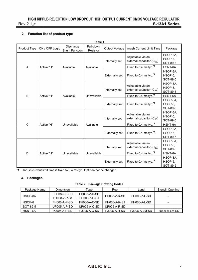
2. Function list of product type
Table 1
Product Type ON / OFF LogicDischarge
Shunt FunctionPull-down Resistor
Output Voltage Inrush Current Limit Time Package
A Active "H" Available Available
Internally set Adjustable via an external capacitor (CSS)
HSOP-8A, HSOP-6, SOT-89-5
Fixed to 0.4 ms typ.*1 HSNT-6A
Externally set Fixed to 0.4 ms typ.*1 HSOP-8A, HSOP-6, SOT-89-5
B Active "H" Available Unavailable
Internally set Adjustable via an external capacitor (CSS)
HSOP-8A, HSOP-6, SOT-89-5
Fixed to 0.4 ms typ.*1 HSNT-6A
Externally set Fixed to 0.4 ms typ.*1 HSOP-8A, HSOP-6, SOT-89-5
C Active "H" Unavailable Available
Internally set Adjustable via an external capacitor (CSS)
HSOP-8A, HSOP-6, SOT-89-5
Fixed to 0.4 ms typ.*1 HSNT-6A
Externally set Fixed to 0.4 ms typ.*1 HSOP-8A, HSOP-6, SOT-89-5
D Active "H" Unavailable Unavailable
Internally set Adjustable via an external capacitor (CSS)
HSOP-8A, HSOP-6, SOT-89-5
Fixed to 0.4 ms typ.*1 HSNT-6A
Externally set Fixed to 0.4 ms typ.*1 HSOP-8A, HSOP-6, SOT-89-5
*1. Inrush current limit time is fixed to 0.4 ms typ. that can not be changed.
3. Packages
Table 2 Package Drawing Codes
Package Name Dimension Tape Reel Land Stencil Opening
HSOP-8A FH008-Z-P-SD FH008-Z-P-S1
FH008-Z-C-SD FH008-Z-C-S1
FH008-Z-R-SD FH008-Z-L-SD
HSOP-6 FH006-A-P-SD FH006-A-C-SD FH006-A-R-S1 FH006-A-L-SD
SOT-89-5 UP005-A-P-SD UP005-A-C-SD UP005-A-R-SD
HSNT-6A PJ006-A-P-SD PJ006-A-C-SD PJ006-A-R-SD PJ006-A-LM-SD PJ006-A-LM-SD
HIGH RIPPLE-REJECTION LOW DROPOUT HIGH OUTPUT CURRENT CMOS VOLTAGE REGULATOR S-13A1 Series Rev.2.1_01
8
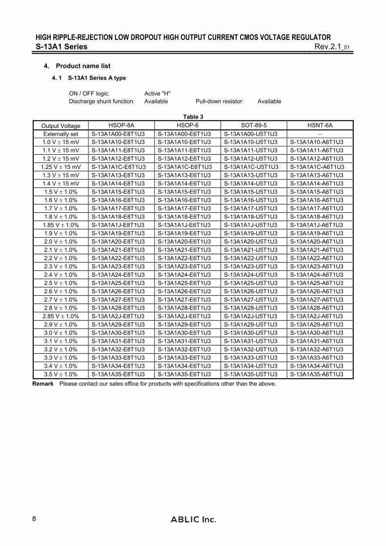
4. Product name list
4. 1 S-13A1 Series A type
ON / OFF logic: Active "H" Discharge shunt function: Available Pull-down resistor: Available
Table 3
Output Voltage HSOP-8A HSOP-6 SOT-89-5 HSNT-6A
Externally set S-13A1A00-E8T1U3 S-13A1A00-E6T1U3 S-13A1A00-U5T1U3 1.0 V 15 mV S-13A1A10-E8T1U3 S-13A1A10-E6T1U3 S-13A1A10-U5T1U3 S-13A1A10-A6T1U3
1.1 V 15 mV S-13A1A11-E8T1U3 S-13A1A11-E6T1U3 S-13A1A11-U5T1U3 S-13A1A11-A6T1U3
1.2 V 15 mV S-13A1A12-E8T1U3 S-13A1A12-E6T1U3 S-13A1A12-U5T1U3 S-13A1A12-A6T1U3
1.25 V 15 mV S-13A1A1C-E8T1U3 S-13A1A1C-E6T1U3 S-13A1A1C-U5T1U3 S-13A1A1C-A6T1U3
1.3 V 15 mV S-13A1A13-E8T1U3 S-13A1A13-E6T1U3 S-13A1A13-U5T1U3 S-13A1A13-A6T1U3
1.4 V 15 mV S-13A1A14-E8T1U3 S-13A1A14-E6T1U3 S-13A1A14-U5T1U3 S-13A1A14-A6T1U3
1.5 V 1.0% S-13A1A15-E8T1U3 S-13A1A15-E6T1U3 S-13A1A15-U5T1U3 S-13A1A15-A6T1U3
1.6 V 1.0% S-13A1A16-E8T1U3 S-13A1A16-E6T1U3 S-13A1A16-U5T1U3 S-13A1A16-A6T1U3
1.7 V 1.0% S-13A1A17-E8T1U3 S-13A1A17-E6T1U3 S-13A1A17-U5T1U3 S-13A1A17-A6T1U3
1.8 V 1.0% S-13A1A18-E8T1U3 S-13A1A18-E6T1U3 S-13A1A18-U5T1U3 S-13A1A18-A6T1U3
1.85 V 1.0% S-13A1A1J-E8T1U3 S-13A1A1J-E6T1U3 S-13A1A1J-U5T1U3 S-13A1A1J-A6T1U3
1.9 V 1.0% S-13A1A19-E8T1U3 S-13A1A19-E6T1U3 S-13A1A19-U5T1U3 S-13A1A19-A6T1U3
2.0 V 1.0% S-13A1A20-E8T1U3 S-13A1A20-E6T1U3 S-13A1A20-U5T1U3 S-13A1A20-A6T1U3
2.1 V 1.0% S-13A1A21-E8T1U3 S-13A1A21-E6T1U3 S-13A1A21-U5T1U3 S-13A1A21-A6T1U3
2.2 V 1.0% S-13A1A22-E8T1U3 S-13A1A22-E6T1U3 S-13A1A22-U5T1U3 S-13A1A22-A6T1U3
2.3 V 1.0% S-13A1A23-E8T1U3 S-13A1A23-E6T1U3 S-13A1A23-U5T1U3 S-13A1A23-A6T1U3
2.4 V 1.0% S-13A1A24-E8T1U3 S-13A1A24-E6T1U3 S-13A1A24-U5T1U3 S-13A1A24-A6T1U3
2.5 V 1.0% S-13A1A25-E8T1U3 S-13A1A25-E6T1U3 S-13A1A25-U5T1U3 S-13A1A25-A6T1U3
2.6 V 1.0% S-13A1A26-E8T1U3 S-13A1A26-E6T1U3 S-13A1A26-U5T1U3 S-13A1A26-A6T1U3
2.7 V 1.0% S-13A1A27-E8T1U3 S-13A1A27-E6T1U3 S-13A1A27-U5T1U3 S-13A1A27-A6T1U3
2.8 V 1.0% S-13A1A28-E8T1U3 S-13A1A28-E6T1U3 S-13A1A28-U5T1U3 S-13A1A28-A6T1U3
2.85 V 1.0% S-13A1A2J-E8T1U3 S-13A1A2J-E6T1U3 S-13A1A2J-U5T1U3 S-13A1A2J-A6T1U3
2.9 V 1.0% S-13A1A29-E8T1U3 S-13A1A29-E6T1U3 S-13A1A29-U5T1U3 S-13A1A29-A6T1U3
3.0 V 1.0% S-13A1A30-E8T1U3 S-13A1A30-E6T1U3 S-13A1A30-U5T1U3 S-13A1A30-A6T1U3
3.1 V 1.0% S-13A1A31-E8T1U3 S-13A1A31-E6T1U3 S-13A1A31-U5T1U3 S-13A1A31-A6T1U3
3.2 V 1.0% S-13A1A32-E8T1U3 S-13A1A32-E6T1U3 S-13A1A32-U5T1U3 S-13A1A32-A6T1U3
3.3 V 1.0% S-13A1A33-E8T1U3 S-13A1A33-E6T1U3 S-13A1A33-U5T1U3 S-13A1A33-A6T1U3
3.4 V 1.0% S-13A1A34-E8T1U3 S-13A1A34-E6T1U3 S-13A1A34-U5T1U3 S-13A1A34-A6T1U3
3.5 V 1.0% S-13A1A35-E8T1U3 S-13A1A35-E6T1U3 S-13A1A35-U5T1U3 S-13A1A35-A6T1U3
Remark Please contact our sales office for products with specifications other than the above.
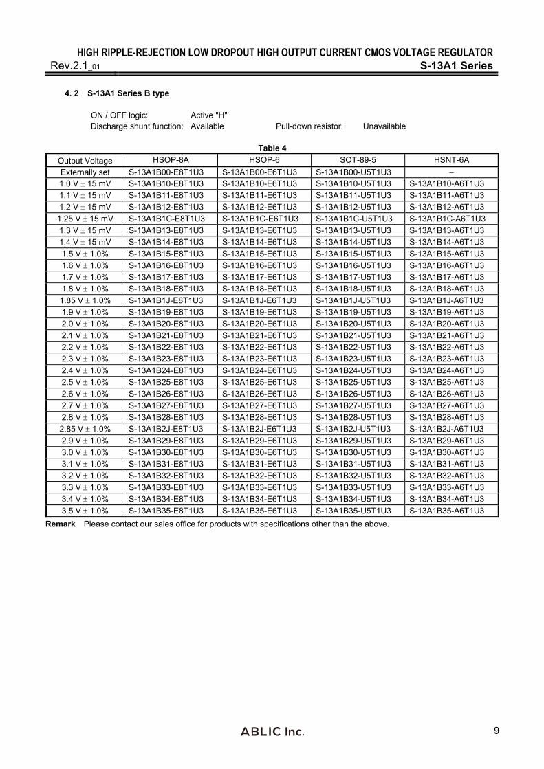
HIGH RIPPLE-REJECTION LOW DROPOUT HIGH OUTPUT CURRENT CMOS VOLTAGE REGULATORRev.2.1_01 S-13A1 Series
9
4. 2 S-13A1 Series B type ON / OFF logic: Active "H" Discharge shunt function: Available Pull-down resistor: Unavailable
Table 4
Output Voltage HSOP-8A HSOP-6 SOT-89-5 HSNT-6A
Externally set S-13A1B00-E8T1U3 S-13A1B00-E6T1U3 S-13A1B00-U5T1U3 1.0 V 15 mV S-13A1B10-E8T1U3 S-13A1B10-E6T1U3 S-13A1B10-U5T1U3 S-13A1B10-A6T1U3
1.1 V 15 mV S-13A1B11-E8T1U3 S-13A1B11-E6T1U3 S-13A1B11-U5T1U3 S-13A1B11-A6T1U3
1.2 V 15 mV S-13A1B12-E8T1U3 S-13A1B12-E6T1U3 S-13A1B12-U5T1U3 S-13A1B12-A6T1U3
1.25 V 15 mV S-13A1B1C-E8T1U3 S-13A1B1C-E6T1U3 S-13A1B1C-U5T1U3 S-13A1B1C-A6T1U3
1.3 V 15 mV S-13A1B13-E8T1U3 S-13A1B13-E6T1U3 S-13A1B13-U5T1U3 S-13A1B13-A6T1U3
1.4 V 15 mV S-13A1B14-E8T1U3 S-13A1B14-E6T1U3 S-13A1B14-U5T1U3 S-13A1B14-A6T1U3
1.5 V 1.0% S-13A1B15-E8T1U3 S-13A1B15-E6T1U3 S-13A1B15-U5T1U3 S-13A1B15-A6T1U3
1.6 V 1.0% S-13A1B16-E8T1U3 S-13A1B16-E6T1U3 S-13A1B16-U5T1U3 S-13A1B16-A6T1U3
1.7 V 1.0% S-13A1B17-E8T1U3 S-13A1B17-E6T1U3 S-13A1B17-U5T1U3 S-13A1B17-A6T1U3
1.8 V 1.0% S-13A1B18-E8T1U3 S-13A1B18-E6T1U3 S-13A1B18-U5T1U3 S-13A1B18-A6T1U3
1.85 V 1.0% S-13A1B1J-E8T1U3 S-13A1B1J-E6T1U3 S-13A1B1J-U5T1U3 S-13A1B1J-A6T1U3
1.9 V 1.0% S-13A1B19-E8T1U3 S-13A1B19-E6T1U3 S-13A1B19-U5T1U3 S-13A1B19-A6T1U3
2.0 V 1.0% S-13A1B20-E8T1U3 S-13A1B20-E6T1U3 S-13A1B20-U5T1U3 S-13A1B20-A6T1U3
2.1 V 1.0% S-13A1B21-E8T1U3 S-13A1B21-E6T1U3 S-13A1B21-U5T1U3 S-13A1B21-A6T1U3
2.2 V 1.0% S-13A1B22-E8T1U3 S-13A1B22-E6T1U3 S-13A1B22-U5T1U3 S-13A1B22-A6T1U3
2.3 V 1.0% S-13A1B23-E8T1U3 S-13A1B23-E6T1U3 S-13A1B23-U5T1U3 S-13A1B23-A6T1U3
2.4 V 1.0% S-13A1B24-E8T1U3 S-13A1B24-E6T1U3 S-13A1B24-U5T1U3 S-13A1B24-A6T1U3
2.5 V 1.0% S-13A1B25-E8T1U3 S-13A1B25-E6T1U3 S-13A1B25-U5T1U3 S-13A1B25-A6T1U3
2.6 V 1.0% S-13A1B26-E8T1U3 S-13A1B26-E6T1U3 S-13A1B26-U5T1U3 S-13A1B26-A6T1U3
2.7 V 1.0% S-13A1B27-E8T1U3 S-13A1B27-E6T1U3 S-13A1B27-U5T1U3 S-13A1B27-A6T1U3
2.8 V 1.0% S-13A1B28-E8T1U3 S-13A1B28-E6T1U3 S-13A1B28-U5T1U3 S-13A1B28-A6T1U3
2.85 V 1.0% S-13A1B2J-E8T1U3 S-13A1B2J-E6T1U3 S-13A1B2J-U5T1U3 S-13A1B2J-A6T1U3
2.9 V 1.0% S-13A1B29-E8T1U3 S-13A1B29-E6T1U3 S-13A1B29-U5T1U3 S-13A1B29-A6T1U3
3.0 V 1.0% S-13A1B30-E8T1U3 S-13A1B30-E6T1U3 S-13A1B30-U5T1U3 S-13A1B30-A6T1U3
3.1 V 1.0% S-13A1B31-E8T1U3 S-13A1B31-E6T1U3 S-13A1B31-U5T1U3 S-13A1B31-A6T1U3
3.2 V 1.0% S-13A1B32-E8T1U3 S-13A1B32-E6T1U3 S-13A1B32-U5T1U3 S-13A1B32-A6T1U3
3.3 V 1.0% S-13A1B33-E8T1U3 S-13A1B33-E6T1U3 S-13A1B33-U5T1U3 S-13A1B33-A6T1U3
3.4 V 1.0% S-13A1B34-E8T1U3 S-13A1B34-E6T1U3 S-13A1B34-U5T1U3 S-13A1B34-A6T1U3
3.5 V 1.0% S-13A1B35-E8T1U3 S-13A1B35-E6T1U3 S-13A1B35-U5T1U3 S-13A1B35-A6T1U3
Remark Please contact our sales office for products with specifications other than the above.
HIGH RIPPLE-REJECTION LOW DROPOUT HIGH OUTPUT CURRENT CMOS VOLTAGE REGULATOR S-13A1 Series Rev.2.1_01
10
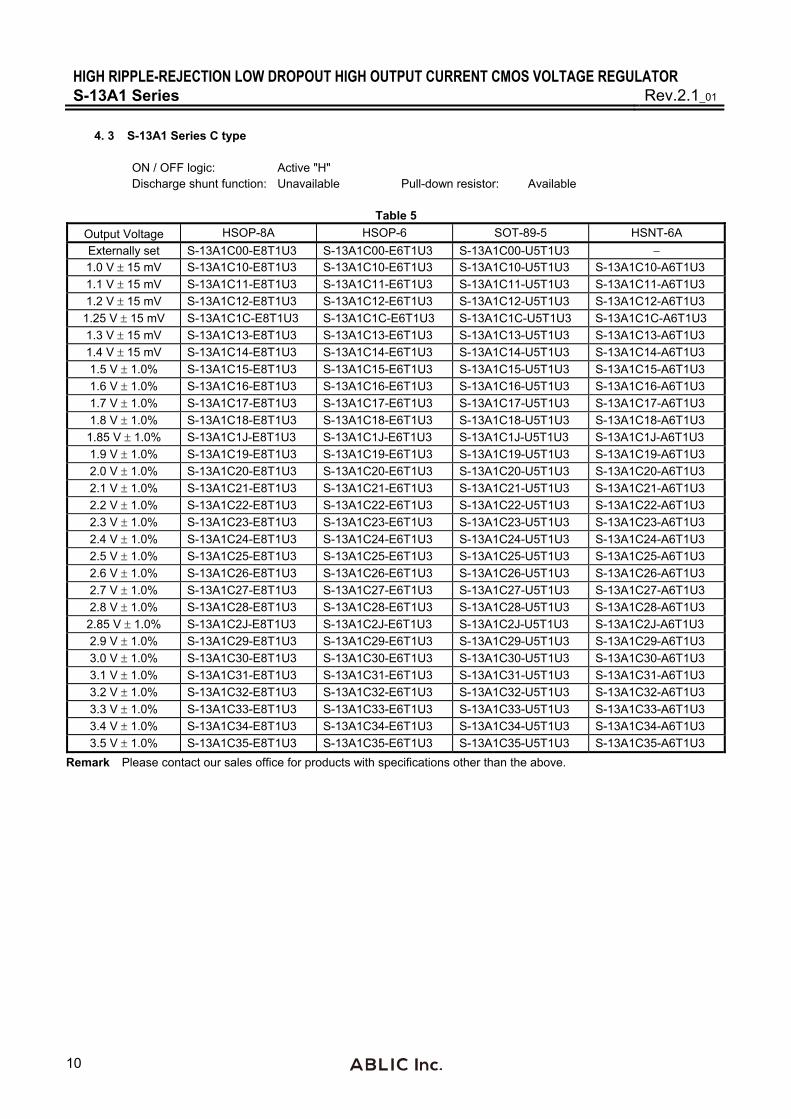
4. 3 S-13A1 Series C type ON / OFF logic: Active "H" Discharge shunt function: Unavailable Pull-down resistor: Available
Table 5
Output Voltage HSOP-8A HSOP-6 SOT-89-5 HSNT-6A
Externally set S-13A1C00-E8T1U3 S-13A1C00-E6T1U3 S-13A1C00-U5T1U3 1.0 V 15 mV S-13A1C10-E8T1U3 S-13A1C10-E6T1U3 S-13A1C10-U5T1U3 S-13A1C10-A6T1U3
1.1 V 15 mV S-13A1C11-E8T1U3 S-13A1C11-E6T1U3 S-13A1C11-U5T1U3 S-13A1C11-A6T1U3
1.2 V 15 mV S-13A1C12-E8T1U3 S-13A1C12-E6T1U3 S-13A1C12-U5T1U3 S-13A1C12-A6T1U3
1.25 V 15 mV S-13A1C1C-E8T1U3 S-13A1C1C-E6T1U3 S-13A1C1C-U5T1U3 S-13A1C1C-A6T1U3
1.3 V 15 mV S-13A1C13-E8T1U3 S-13A1C13-E6T1U3 S-13A1C13-U5T1U3 S-13A1C13-A6T1U3
1.4 V 15 mV S-13A1C14-E8T1U3 S-13A1C14-E6T1U3 S-13A1C14-U5T1U3 S-13A1C14-A6T1U3
1.5 V 1.0% S-13A1C15-E8T1U3 S-13A1C15-E6T1U3 S-13A1C15-U5T1U3 S-13A1C15-A6T1U3
1.6 V 1.0% S-13A1C16-E8T1U3 S-13A1C16-E6T1U3 S-13A1C16-U5T1U3 S-13A1C16-A6T1U3
1.7 V 1.0% S-13A1C17-E8T1U3 S-13A1C17-E6T1U3 S-13A1C17-U5T1U3 S-13A1C17-A6T1U3
1.8 V 1.0% S-13A1C18-E8T1U3 S-13A1C18-E6T1U3 S-13A1C18-U5T1U3 S-13A1C18-A6T1U3
1.85 V 1.0% S-13A1C1J-E8T1U3 S-13A1C1J-E6T1U3 S-13A1C1J-U5T1U3 S-13A1C1J-A6T1U3
1.9 V 1.0% S-13A1C19-E8T1U3 S-13A1C19-E6T1U3 S-13A1C19-U5T1U3 S-13A1C19-A6T1U3
2.0 V 1.0% S-13A1C20-E8T1U3 S-13A1C20-E6T1U3 S-13A1C20-U5T1U3 S-13A1C20-A6T1U3
2.1 V 1.0% S-13A1C21-E8T1U3 S-13A1C21-E6T1U3 S-13A1C21-U5T1U3 S-13A1C21-A6T1U3
2.2 V 1.0% S-13A1C22-E8T1U3 S-13A1C22-E6T1U3 S-13A1C22-U5T1U3 S-13A1C22-A6T1U3
2.3 V 1.0% S-13A1C23-E8T1U3 S-13A1C23-E6T1U3 S-13A1C23-U5T1U3 S-13A1C23-A6T1U3
2.4 V 1.0% S-13A1C24-E8T1U3 S-13A1C24-E6T1U3 S-13A1C24-U5T1U3 S-13A1C24-A6T1U3
2.5 V 1.0% S-13A1C25-E8T1U3 S-13A1C25-E6T1U3 S-13A1C25-U5T1U3 S-13A1C25-A6T1U3
2.6 V 1.0% S-13A1C26-E8T1U3 S-13A1C26-E6T1U3 S-13A1C26-U5T1U3 S-13A1C26-A6T1U3
2.7 V 1.0% S-13A1C27-E8T1U3 S-13A1C27-E6T1U3 S-13A1C27-U5T1U3 S-13A1C27-A6T1U3
2.8 V 1.0% S-13A1C28-E8T1U3 S-13A1C28-E6T1U3 S-13A1C28-U5T1U3 S-13A1C28-A6T1U3
2.85 V 1.0% S-13A1C2J-E8T1U3 S-13A1C2J-E6T1U3 S-13A1C2J-U5T1U3 S-13A1C2J-A6T1U3
2.9 V 1.0% S-13A1C29-E8T1U3 S-13A1C29-E6T1U3 S-13A1C29-U5T1U3 S-13A1C29-A6T1U3
3.0 V 1.0% S-13A1C30-E8T1U3 S-13A1C30-E6T1U3 S-13A1C30-U5T1U3 S-13A1C30-A6T1U3
3.1 V 1.0% S-13A1C31-E8T1U3 S-13A1C31-E6T1U3 S-13A1C31-U5T1U3 S-13A1C31-A6T1U3
3.2 V 1.0% S-13A1C32-E8T1U3 S-13A1C32-E6T1U3 S-13A1C32-U5T1U3 S-13A1C32-A6T1U3
3.3 V 1.0% S-13A1C33-E8T1U3 S-13A1C33-E6T1U3 S-13A1C33-U5T1U3 S-13A1C33-A6T1U3
3.4 V 1.0% S-13A1C34-E8T1U3 S-13A1C34-E6T1U3 S-13A1C34-U5T1U3 S-13A1C34-A6T1U3
3.5 V 1.0% S-13A1C35-E8T1U3 S-13A1C35-E6T1U3 S-13A1C35-U5T1U3 S-13A1C35-A6T1U3
Remark Please contact our sales office for products with specifications other than the above.

HIGH RIPPLE-REJECTION LOW DROPOUT HIGH OUTPUT CURRENT CMOS VOLTAGE REGULATORRev.2.1_01 S-13A1 Series
11
4. 4 S-13A1 Series D type ON / OFF logic: Active "H" Discharge shunt function: Unavailable Pull-down resistor: Unavailable
Table 6
Output Voltage HSOP-8A HSOP-6 SOT-89-5 HSNT-6A
Externally set S-13A1D00-E8T1U3 S-13A1D00-E6T1U3 S-13A1D00-U5T1U3 1.0 V 15 mV S-13A1D10-E8T1U3 S-13A1D10-E6T1U3 S-13A1D10-U5T1U3 S-13A1D10-A6T1U3
1.1 V 15 mV S-13A1D11-E8T1U3 S-13A1D11-E6T1U3 S-13A1D11-U5T1U3 S-13A1D11-A6T1U3
1.2 V 15 mV S-13A1D12-E8T1U3 S-13A1D12-E6T1U3 S-13A1D12-U5T1U3 S-13A1D12-A6T1U3
1.25 V 15 mV S-13A1D1C-E8T1U3 S-13A1D1C-E6T1U3 S-13A1D1C-U5T1U3 S-13A1D1C-A6T1U3
1.3 V 15 mV S-13A1D13-E8T1U3 S-13A1D13-E6T1U3 S-13A1D13-U5T1U3 S-13A1D13-A6T1U3
1.4 V 15 mV S-13A1D14-E8T1U3 S-13A1D14-E6T1U3 S-13A1D14-U5T1U3 S-13A1D14-A6T1U3
1.5 V 1.0% S-13A1D15-E8T1U3 S-13A1D15-E6T1U3 S-13A1D15-U5T1U3 S-13A1D15-A6T1U3
1.6 V 1.0% S-13A1D16-E8T1U3 S-13A1D16-E6T1U3 S-13A1D16-U5T1U3 S-13A1D16-A6T1U3
1.7 V 1.0% S-13A1D17-E8T1U3 S-13A1D17-E6T1U3 S-13A1D17-U5T1U3 S-13A1D17-A6T1U3
1.8 V 1.0% S-13A1D18-E8T1U3 S-13A1D18-E6T1U3 S-13A1D18-U5T1U3 S-13A1D18-A6T1U3
1.85 V 1.0% S-13A1D1J-E8T1U3 S-13A1D1J-E6T1U3 S-13A1D1J-U5T1U3 S-13A1D1J-A6T1U3
1.9 V 1.0% S-13A1D19-E8T1U3 S-13A1D19-E6T1U3 S-13A1D19-U5T1U3 S-13A1D19-A6T1U3
2.0 V 1.0% S-13A1D20-E8T1U3 S-13A1D20-E6T1U3 S-13A1D20-U5T1U3 S-13A1D20-A6T1U3
2.1 V 1.0% S-13A1D21-E8T1U3 S-13A1D21-E6T1U3 S-13A1D21-U5T1U3 S-13A1D21-A6T1U3
2.2 V 1.0% S-13A1D22-E8T1U3 S-13A1D22-E6T1U3 S-13A1D22-U5T1U3 S-13A1D22-A6T1U3
2.3 V 1.0% S-13A1D23-E8T1U3 S-13A1D23-E6T1U3 S-13A1D23-U5T1U3 S-13A1D23-A6T1U3
2.4 V 1.0% S-13A1D24-E8T1U3 S-13A1D24-E6T1U3 S-13A1D24-U5T1U3 S-13A1D24-A6T1U3
2.5 V 1.0% S-13A1D25-E8T1U3 S-13A1D25-E6T1U3 S-13A1D25-U5T1U3 S-13A1D25-A6T1U3
2.6 V 1.0% S-13A1D26-E8T1U3 S-13A1D26-E6T1U3 S-13A1D26-U5T1U3 S-13A1D26-A6T1U3
2.7 V 1.0% S-13A1D27-E8T1U3 S-13A1D27-E6T1U3 S-13A1D27-U5T1U3 S-13A1D27-A6T1U3
2.8 V 1.0% S-13A1D28-E8T1U3 S-13A1D28-E6T1U3 S-13A1D28-U5T1U3 S-13A1D28-A6T1U3
2.85 V 1.0% S-13A1D2J-E8T1U3 S-13A1D2J-E6T1U3 S-13A1D2J-U5T1U3 S-13A1D2J-A6T1U3
2.9 V 1.0% S-13A1D29-E8T1U3 S-13A1D29-E6T1U3 S-13A1D29-U5T1U3 S-13A1D29-A6T1U3
3.0 V 1.0% S-13A1D30-E8T1U3 S-13A1D30-E6T1U3 S-13A1D30-U5T1U3 S-13A1D30-A6T1U3
3.1 V 1.0% S-13A1D31-E8T1U3 S-13A1D31-E6T1U3 S-13A1D31-U5T1U3 S-13A1D31-A6T1U3
3.2 V 1.0% S-13A1D32-E8T1U3 S-13A1D32-E6T1U3 S-13A1D32-U5T1U3 S-13A1D32-A6T1U3
3.3 V 1.0% S-13A1D33-E8T1U3 S-13A1D33-E6T1U3 S-13A1D33-U5T1U3 S-13A1D33-A6T1U3
3.4 V 1.0% S-13A1D34-E8T1U3 S-13A1D34-E6T1U3 S-13A1D34-U5T1U3 S-13A1D34-A6T1U3
3.5 V 1.0% S-13A1D35-E8T1U3 S-13A1D35-E6T1U3 S-13A1D35-U5T1U3 S-13A1D35-A6T1U3
Remark Please contact our sales office for products with specifications other than the above.
HIGH RIPPLE-REJECTION LOW DROPOUT HIGH OUTPUT CURRENT CMOS VOLTAGE REGULATOR S-13A1 Series Rev.2.1_01
12
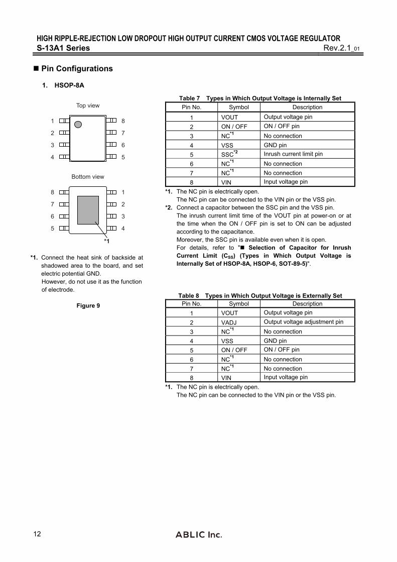
Pin Configurations 1. HSOP-8A
8
5
6
7
1
4
3
2
Bottom view
Top view
1
4
3
2
8
5
6
7
*1
*1. Connect the heat sink of backside at shadowed area to the board, and set electric potential GND. However, do not use it as the function of electrode.
Figure 9
Table 7 Types in Which Output Voltage is Internally Set
Pin No. Symbol Description
1 VOUT Output voltage pin
2 ON / OFF ON / OFF pin
3 NC*1 No connection
4 VSS GND pin
5 SSC*2 Inrush current limit pin
6 NC*1 No connection
7 NC*1 No connection
8 VIN Input voltage pin
*1. The NC pin is electrically open. The NC pin can be connected to the VIN pin or the VSS pin.
*2. Connect a capacitor between the SSC pin and the VSS pin. The inrush current limit time of the VOUT pin at power-on or at the time when the ON / OFF pin is set to ON can be adjusted according to the capacitance. Moreover, the SSC pin is available even when it is open. For details, refer to " Selection of Capacitor for Inrush Current Limit (CSS) (Types in Which Output Voltage is Internally Set of HSOP-8A, HSOP-6, SOT-89-5)".
Table 8 Types in Which Output Voltage is Externally Set Pin No. Symbol Description
1 VOUT Output voltage pin
2 VADJ Output voltage adjustment pin
3 NC*1 No connection
4 VSS GND pin
5 ON / OFF ON / OFF pin
6 NC*1 No connection
7 NC*1 No connection
8 VIN Input voltage pin
*1. The NC pin is electrically open. The NC pin can be connected to the VIN pin or the VSS pin.
HIGH RIPPLE-REJECTION LOW DROPOUT HIGH OUTPUT CURRENT CMOS VOLTAGE REGULATORRev.2.1_01 S-13A1 Series
13
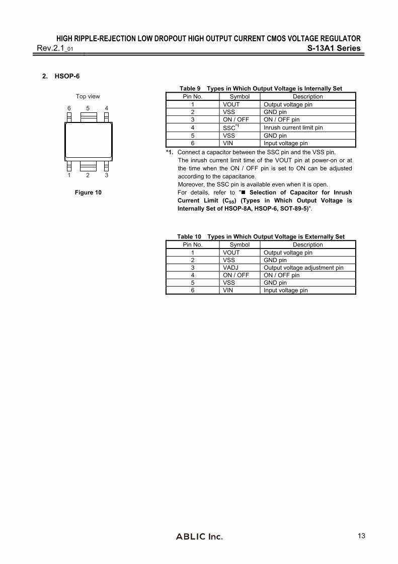
2. HSOP-6
1 32
46 5
Top view
Figure 10
Table 9 Types in Which Output Voltage is Internally Set Pin No. Symbol Description
1 VOUT Output voltage pin 2 VSS GND pin 3 ON / OFF ON / OFF pin 4 SSC*1 Inrush current limit pin 5 VSS GND pin 6 VIN Input voltage pin
*1. Connect a capacitor between the SSC pin and the VSS pin. The inrush current limit time of the VOUT pin at power-on or at the time when the ON / OFF pin is set to ON can be adjusted according to the capacitance. Moreover, the SSC pin is available even when it is open. For details, refer to " Selection of Capacitor for Inrush Current Limit (CSS) (Types in Which Output Voltage is Internally Set of HSOP-8A, HSOP-6, SOT-89-5)".
Table 10 Types in Which Output Voltage is Externally Set Pin No. Symbol Description
1 VOUT Output voltage pin 2 VSS GND pin 3 VADJ Output voltage adjustment pin 4 ON / OFF ON / OFF pin 5 VSS GND pin 6 VIN Input voltage pin
HIGH RIPPLE-REJECTION LOW DROPOUT HIGH OUTPUT CURRENT CMOS VOLTAGE REGULATOR S-13A1 Series Rev.2.1_01
14
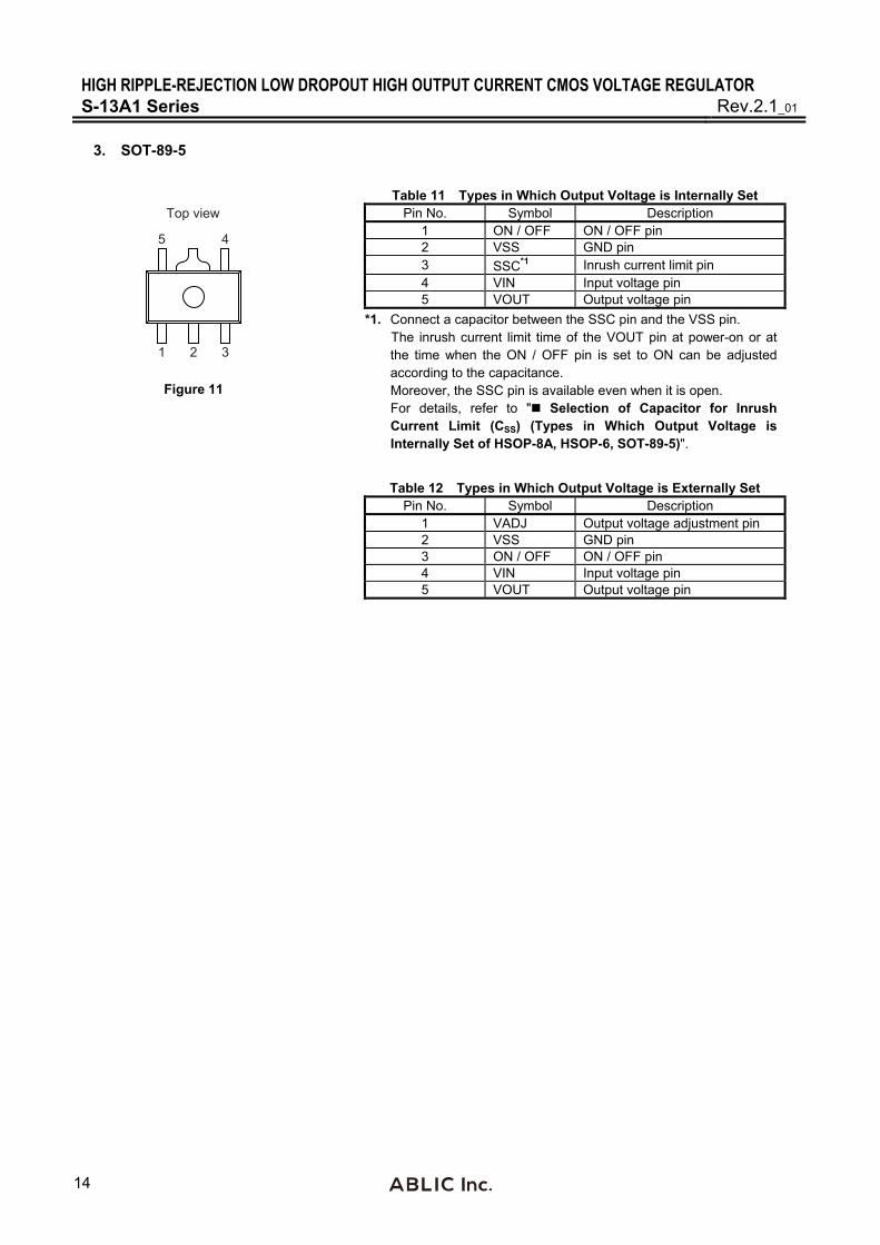
3. SOT-89-5
1 32
45
Top view
Figure 11
Table 11 Types in Which Output Voltage is Internally Set Pin No. Symbol Description
1 ON / OFF ON / OFF pin 2 VSS GND pin 3 SSC*1 Inrush current limit pin 4 VIN Input voltage pin 5 VOUT Output voltage pin
*1. Connect a capacitor between the SSC pin and the VSS pin. The inrush current limit time of the VOUT pin at power-on or at the time when the ON / OFF pin is set to ON can be adjusted according to the capacitance. Moreover, the SSC pin is available even when it is open. For details, refer to " Selection of Capacitor for Inrush Current Limit (CSS) (Types in Which Output Voltage is Internally Set of HSOP-8A, HSOP-6, SOT-89-5)".
Table 12 Types in Which Output Voltage is Externally Set Pin No. Symbol Description
1 VADJ Output voltage adjustment pin 2 VSS GND pin 3 ON / OFF ON / OFF pin 4 VIN Input voltage pin 5 VOUT Output voltage pin
HIGH RIPPLE-REJECTION LOW DROPOUT HIGH OUTPUT CURRENT CMOS VOLTAGE REGULATORRev.2.1_01 S-13A1 Series
15
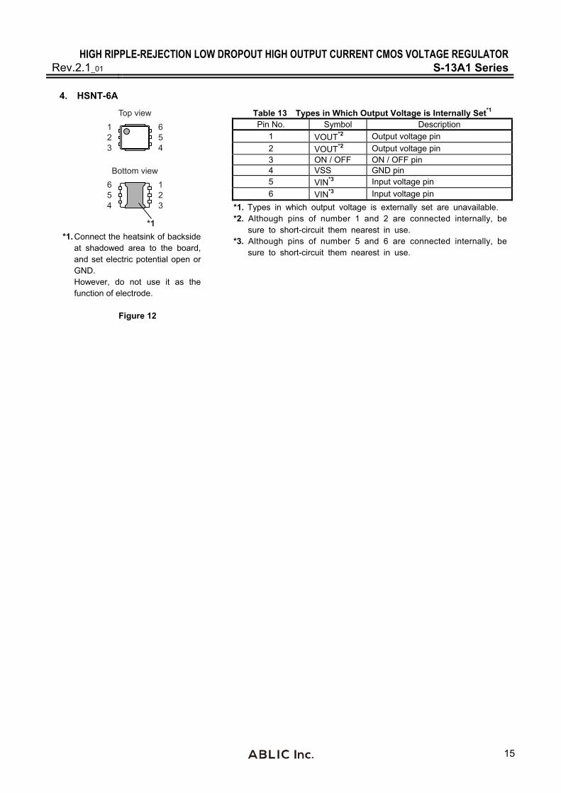
4. HSNT-6A
54
6
23
1
23
1
54
6
Top view
Bottom view
*1 *1. Connect the heatsink of backside
at shadowed area to the board, and set electric potential open or GND. However, do not use it as the function of electrode.
Figure 12
Table 13 Types in Which Output Voltage is Internally Set*1 Pin No. Symbol Description
1 VOUT*2 Output voltage pin
2 VOUT*2 Output voltage pin 3 ON / OFF ON / OFF pin 4 VSS GND pin 5 VIN*3 Input voltage pin
6 VIN*3 Input voltage pin
*1. Types in which output voltage is externally set are unavailable. *2. Although pins of number 1 and 2 are connected internally, be
sure to short-circuit them nearest in use. *3. Although pins of number 5 and 6 are connected internally, be
sure to short-circuit them nearest in use.
HIGH RIPPLE-REJECTION LOW DROPOUT HIGH OUTPUT CURRENT CMOS VOLTAGE REGULATOR S-13A1 Series Rev.2.1_01
16
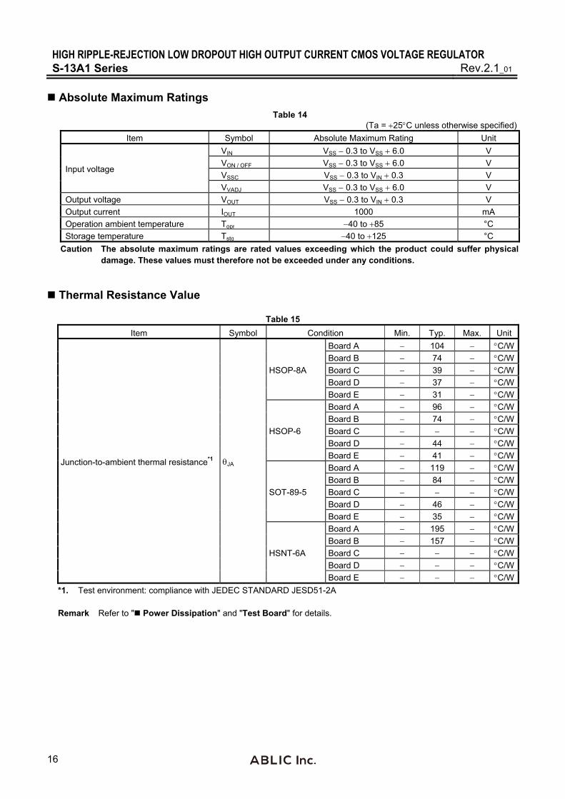
Absolute Maximum Ratings
Table 14 (Ta = 25C unless otherwise specified)
Item Symbol Absolute Maximum Rating Unit
Input voltage
VIN VSS 0.3 to VSS 6.0 V
VON / OFF VSS 0.3 to VSS 6.0 V
VSSC VSS 0.3 to VIN 0.3 V
VVADJ VSS 0.3 to VSS 6.0 V
Output voltage VOUT VSS 0.3 to VIN 0.3 V
Output current IOUT 1000 mA
Operation ambient temperature Topr 40 to 85 °C
Storage temperature Tstg 40 to 125 °C
Caution The absolute maximum ratings are rated values exceeding which the product could suffer physical damage. These values must therefore not be exceeded under any conditions.
Thermal Resistance Value
Table 15
Item Symbol Condition Min. Typ. Max. Unit
Junction-to-ambient thermal resistance*1 JA
HSOP-8A
Board A 104 C/W
Board B 74 C/W
Board C 39 C/W
Board D 37 C/W
Board E 31 C/W
HSOP-6
Board A 96 C/W
Board B 74 C/W
Board C C/W
Board D 44 C/W
Board E 41 C/W
SOT-89-5
Board A 119 C/W
Board B 84 C/W
Board C C/W
Board D 46 C/W
Board E 35 C/W
HSNT-6A
Board A 195 C/W
Board B 157 C/W
Board C C/W
Board D C/W
Board E C/W
*1. Test environment: compliance with JEDEC STANDARD JESD51-2A
Remark Refer to " Power Dissipation" and "Test Board" for details.
HIGH RIPPLE-REJECTION LOW DROPOUT HIGH OUTPUT CURRENT CMOS VOLTAGE REGULATORRev.2.1_01 S-13A1 Series
17
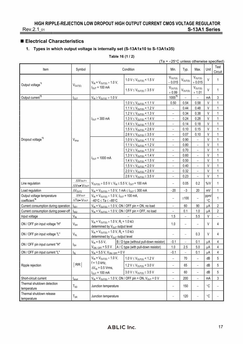
Electrical Characteristics
1. Types in which output voltage is internally set (S-13A1x10 to S-13A1x35)
Table 16 (1 / 2) (Ta = 25C unless otherwise specified)
Item Symbol Condition Min. Typ. Max. UnitTest
Circuit
Output voltage*1 VOUT(E) VIN = VOUT(S) 1.0 V, IOUT = 100 mA
1.0 V VOUT(S) < 1.5 V VOUT(S)
0.015 VOUT(S)
VOUT(S)
0.015V 1
1.5 V VOUT(S) 3.5 V VOUT(S)
0.99 VOUT(S)
VOUT(S)
1.01V 1
Output current*2 IOUT VIN VOUT(S) 1.0 V 1000*5 mA 3
Dropout voltage*3 Vdrop
IOUT = 300 mA
1.0 V VOUT(S) < 1.1 V 0.50 0.54 0.58 V 1
1.1 V VOUT(S) < 1.2 V 0.44 0.48 V 1
1.2 V VOUT(S) < 1.3 V 0.34 0.38 V 1
1.3 V VOUT(S) < 1.4 V 0.24 0.28 V 1
1.4 V VOUT(S) < 1.5 V 0.14 0.18 V 1
1.5 V VOUT(S) < 2.6 V 0.10 0.15 V 1
2.6 V VOUT(S) 3.5 V 0.07 0.10 V 1
IOUT = 1000 mA
1.0 V VOUT(S) < 1.1 V 0.90 V 1
1.1 V VOUT(S) < 1.2 V 0.80 V 1
1.2 V VOUT(S) < 1.3 V 0.70 V 1
1.3 V VOUT(S) < 1.4 V 0.60 V 1
1.4 V VOUT(S) < 1.5 V 0.50 V 1
1.5 V VOUT(S) < 2.0 V 0.40 V 1
2.0 V VOUT(S) < 2.6 V 0.32 V 1
2.6 V VOUT(S) 3.5 V 0.23 V 1
Line regulation OUTIN
OUT1
VV
V
VOUT(S) 0.5 V VIN 5.5 V, IOUT = 100 mA 0.05 0.2 %/V 1
Load regulation VOUT2 VIN = VOUT(S) 1.0 V, 1 mA IOUT 300 mA 20 3 20 mV 1
Output voltage temperature coefficient*4 OUT
OUT
VTa
V
VIN = VOUT(S) 1.0 V, IOUT = 100 mA,
40C Ta 85C 100
ppm/C
1
Current consumption during operation ISS1 VIN = VOUT(S) 1.0 V, ON / OFF pin = ON, no load 60 90 A 2
Current consumption during power-off ISS2 VIN = VOUT(S) 1.0 V, ON / OFF pin = OFF, no load 0.1 1.0 A 2
Input voltage VIN 1.5 5.5 V
ON / OFF pin input voltage "H" VSH VIN = VOUT(S) 1.0 V, RL = 1.0 k determined by VOUT output level
1.0 V 4
ON / OFF pin input voltage "L" VSL VIN = VOUT(S) 1.0 V, RL = 1.0 k determined by VOUT output level
0.3 V 4
ON / OFF pin input current "H" ISH VIN = 5.5 V, VON / OFF = 5.5 V
B / D type (without pull-down resistor) 0.1 0.1 A 4
A / C type (with pull-down resistor) 1.0 2.5 5.0 A 4
ON / OFF pin input current "L" ISL VIN = 5.5 V, VON / OFF = 0 V 0.1 0.1 A 4
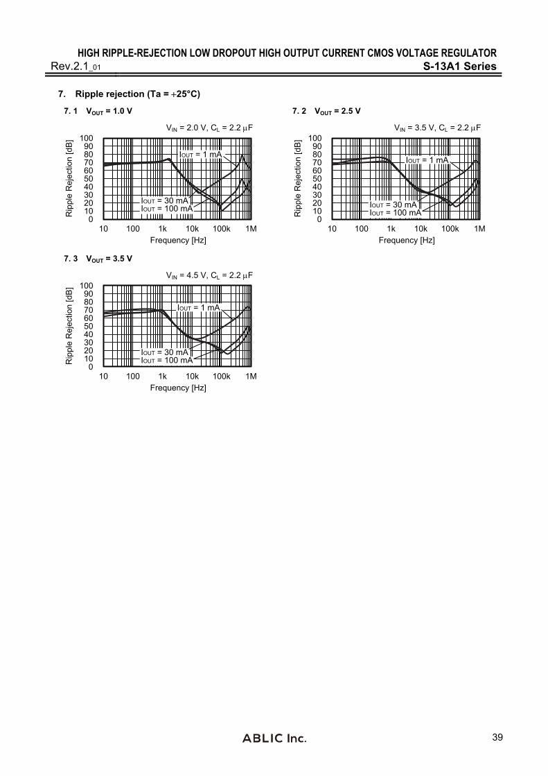
Ripple rejection RR
VIN = VOUT(S) 1.0 V, f = 1.0 kHz, Vrip = 0.5 Vrms, IOUT = 100 mA
1.0 V VOUT(S) < 1.2 V 70 dB 5
1.2 V VOUT(S) < 3.0 V 65 dB 5
3.0 V VOUT(S) 3.5 V 60 dB 5
Short-circuit current Ishort VIN = VOUT(S) 1.0 V, ON / OFF pin = ON, VOUT = 0 V 200 mA 3
Thermal shutdown detection temperature
TSD Junction temperature 150 C
Thermal shutdown release temperature
TSR Junction temperature 120 C
HIGH RIPPLE-REJECTION LOW DROPOUT HIGH OUTPUT CURRENT CMOS VOLTAGE REGULATOR S-13A1 Series Rev.2.1_01
18
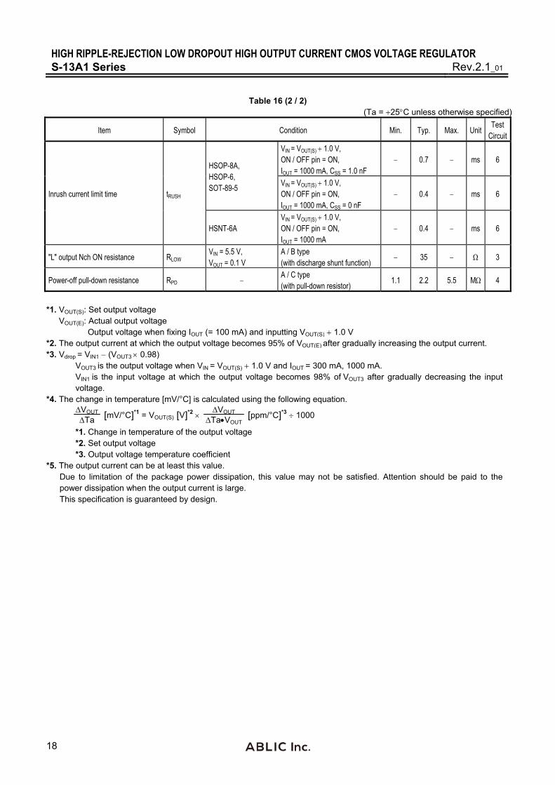
Table 16 (2 / 2) (Ta = 25C unless otherwise specified)
Item Symbol Condition Min. Typ. Max. UnitTest
Circuit
Inrush current limit time tRUSH
HSOP-8A, HSOP-6, SOT-89-5
VIN = VOUT(S) 1.0 V, ON / OFF pin = ON, IOUT = 1000 mA, CSS = 1.0 nF
0.7 ms 6
VIN = VOUT(S) 1.0 V, ON / OFF pin = ON, IOUT = 1000 mA, CSS = 0 nF
0.4 ms 6
HSNT-6A VIN = VOUT(S) 1.0 V, ON / OFF pin = ON, IOUT = 1000 mA
0.4 ms 6
"L" output Nch ON resistance RLOW VIN = 5.5 V, VOUT = 0.1 V
A / B type (with discharge shunt function)
35 3
Power-off pull-down resistance RPD A / C type (with pull-down resistor)
1.1 2.2 5.5 M 4
*1. VOUT(S): Set output voltage
VOUT(E): Actual output voltage Output voltage when fixing IOUT (= 100 mA) and inputting VOUT(S) 1.0 V
*2. The output current at which the output voltage becomes 95% of VOUT(E) after gradually increasing the output current. *3. Vdrop = VIN1 (VOUT3 0.98) VOUT3 is the output voltage when VIN = VOUT(S) 1.0 V and IOUT = 300 mA, 1000 mA.
VIN1 is the input voltage at which the output voltage becomes 98% of VOUT3 after gradually decreasing the input voltage.
*4. The change in temperature [mV/°C] is calculated using the following equation.
VOUT
Ta [ ]mV/°C *1 = VOUT(S) [ ]V *2
VOUT
TaVOUT [ ]ppm/°C *3 1000
*1. Change in temperature of the output voltage *2. Set output voltage *3. Output voltage temperature coefficient
*5. The output current can be at least this value. Due to limitation of the package power dissipation, this value may not be satisfied. Attention should be paid to the
power dissipation when the output current is large. This specification is guaranteed by design.
HIGH RIPPLE-REJECTION LOW DROPOUT HIGH OUTPUT CURRENT CMOS VOLTAGE REGULATORRev.2.1_01 S-13A1 Series
19
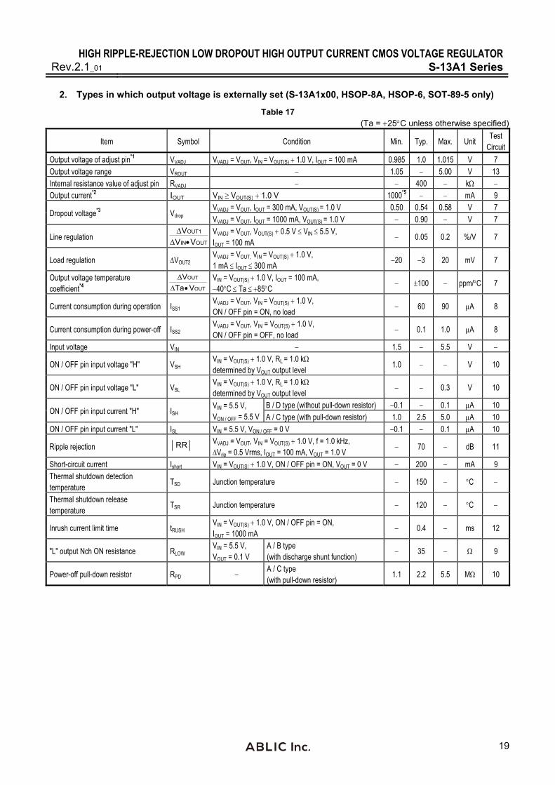
2. Types in which output voltage is externally set (S-13A1x00, HSOP-8A, HSOP-6, SOT-89-5 only)
Table 17 (Ta = 25C unless otherwise specified)
Item Symbol Condition Min. Typ. Max. UnitTest
Circuit
Output voltage of adjust pin*1 VVADJ VVADJ = VOUT, VIN = VOUT(S) 1.0 V, IOUT = 100 mA 0.985 1.0 1.015 V 7
Output voltage range VROUT 1.05 5.00 V 13
Internal resistance value of adjust pin RVADJ 400 k
Output current*2 IOUT VIN VOUT(S) 1.0 V 1000*5 mA 9
Dropout voltage*3 Vdrop VVADJ = VOUT, IOUT = 300 mA, VOUT(S) = 1.0 V 0.50 0.54 0.58 V 7
VVADJ = VOUT, IOUT = 1000 mA, VOUT(S) = 1.0 V 0.90 V 7
Line regulation OUTIN
OUT1
VV
V
VVADJ = VOUT, VOUT(S) 0.5 V VIN 5.5 V, IOUT = 100 mA
0.05 0.2 %/V 7
Load regulation VOUT2 VVADJ = VOUT, VIN = VOUT(S) 1.0 V, 1 mA IOUT 300 mA
20 3 20 mV 7
Output voltage temperature coefficient*4 OUT
OUT
VTa
V
VIN = VOUT(S) 1.0 V, IOUT = 100 mA,
40C Ta 85C 100 ppm/C 7
Current consumption during operation ISS1 VVADJ = VOUT, VIN = VOUT(S) 1.0 V, ON / OFF pin = ON, no load
60 90 A 8
Current consumption during power-off ISS2 VVADJ = VOUT, VIN = VOUT(S) 1.0 V, ON / OFF pin = OFF, no load
0.1 1.0 A 8
Input voltage VIN 1.5 5.5 V
ON / OFF pin input voltage "H" VSH VIN = VOUT(S) 1.0 V, RL = 1.0 k determined by VOUT output level
1.0 V 10
ON / OFF pin input voltage "L" VSL VIN = VOUT(S) 1.0 V, RL = 1.0 k determined by VOUT output level
0.3 V 10
ON / OFF pin input current "H" ISH VIN = 5.5 V, VON / OFF = 5.5 V
B / D type (without pull-down resistor) 0.1 0.1 A 10
A / C type (with pull-down resistor) 1.0 2.5 5.0 A 10
ON / OFF pin input current "L" ISL VIN = 5.5 V, VON / OFF = 0 V 0.1 0.1 A 10
Ripple rejection RR
VVADJ = VOUT, VIN = VOUT(S) 1.0 V, f = 1.0 kHz, Vrip = 0.5 Vrms, IOUT = 100 mA, VOUT = 1.0 V
70 dB 11
Short-circuit current Ishort VIN = VOUT(S) 1.0 V, ON / OFF pin = ON, VOUT = 0 V 200 mA 9
Thermal shutdown detection temperature
TSD Junction temperature 150 C
Thermal shutdown release temperature
TSR Junction temperature 120 C
Inrush current limit time tRUSH VIN = VOUT(S) 1.0 V, ON / OFF pin = ON, IOUT = 1000 mA
0.4 ms 12
"L" output Nch ON resistance RLOW VIN = 5.5 V, VOUT = 0.1 V
A / B type (with discharge shunt function)
35 9
Power-off pull-down resistor RPD A / C type (with pull-down resistor)
1.1 2.2 5.5 M 10
HIGH RIPPLE-REJECTION LOW DROPOUT HIGH OUTPUT CURRENT CMOS VOLTAGE REGULATOR S-13A1 Series Rev.2.1_01
20
*1. VOUT(S): Set output voltage ( = 1.0 V)
*2. The output current at which the output voltage becomes 95% of VVADJ after gradually increasing the output current. *3. Vdrop = VIN1 (VOUT3 0.98) VOUT3 is the output voltage when VIN = VOUT(S) 1.0 V and IOUT = 300 mA, 1000 mA.
VIN1 is the input voltage at which the output voltage becomes 98% of VOUT3 after gradually decreasing the input voltage.
*4. The change in temperature [mV/°C] is calculated using the following equation.
VOUT
Ta [ ]mV/°C *1 = VOUT(S) [ ]V *2
VOUT
TaVOUT [ ]ppm/°C *3 1000
*1. Change in temperature of the output voltage *2. Set output voltage *3. Output voltage temperature coefficient
*5. The output current can be at least this value. Due to limitation of the package power dissipation, this value may not be satisfied. Attention should be paid to the
power dissipation when the output current is large. This specification is guaranteed by design.
HIGH RIPPLE-REJECTION LOW DROPOUT HIGH OUTPUT CURRENT CMOS VOLTAGE REGULATORRev.2.1_01 S-13A1 Series
21
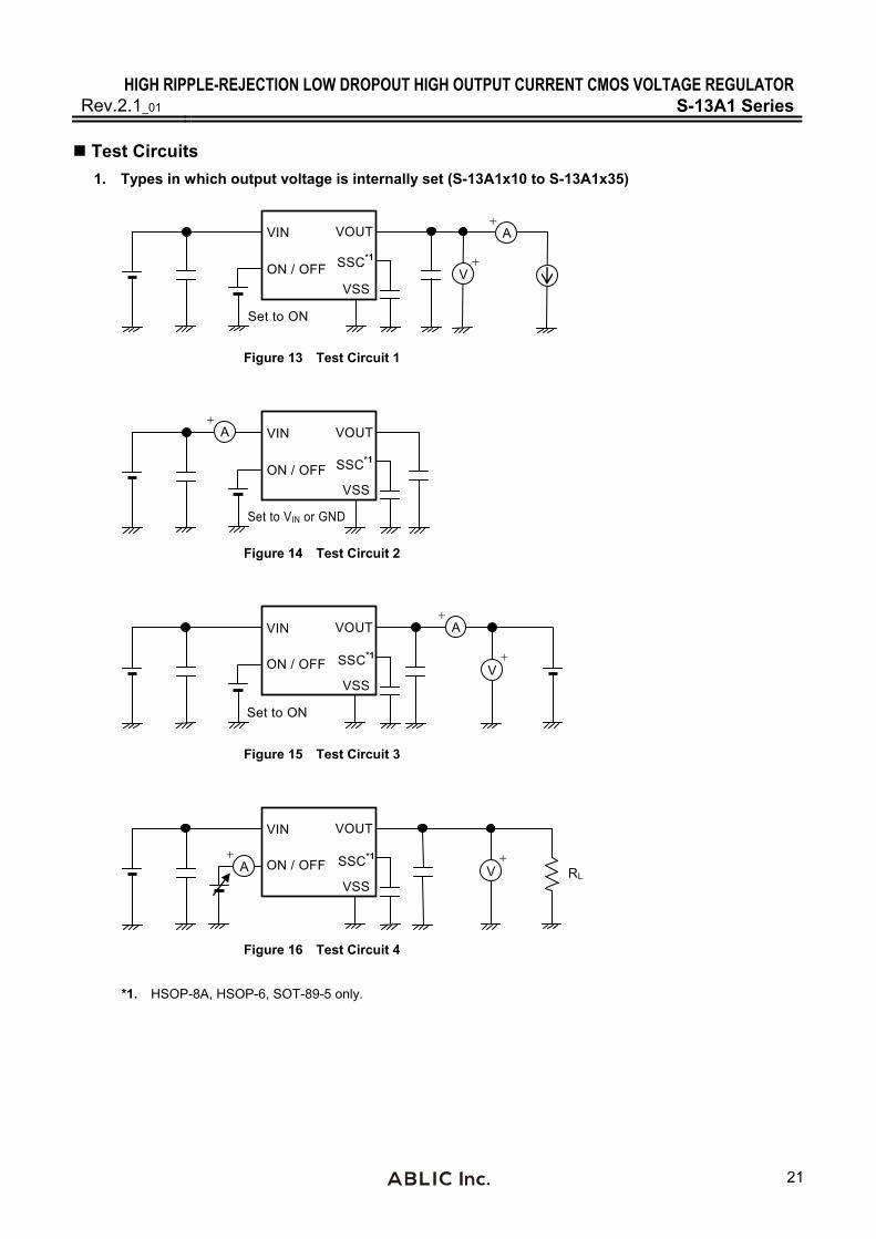
Test Circuits
1. Types in which output voltage is internally set (S-13A1x10 to S-13A1x35)
VOUTVIN
VSS
V
A
ON / OFF
Set to ON
SSC*1
Figure 13 Test Circuit 1
VOUTVIN
Set to VIN or GND
A
ON / OFF
VSS
SSC*1
Figure 14 Test Circuit 2
Set to ON
VOUTVIN
V
A
ON / OFF
VSS
SSC*1
Figure 15 Test Circuit 3
VOUTVIN
V ON / OFF
VSS
A RL
SSC*1
Figure 16 Test Circuit 4
*1. HSOP-8A, HSOP-6, SOT-89-5 only.
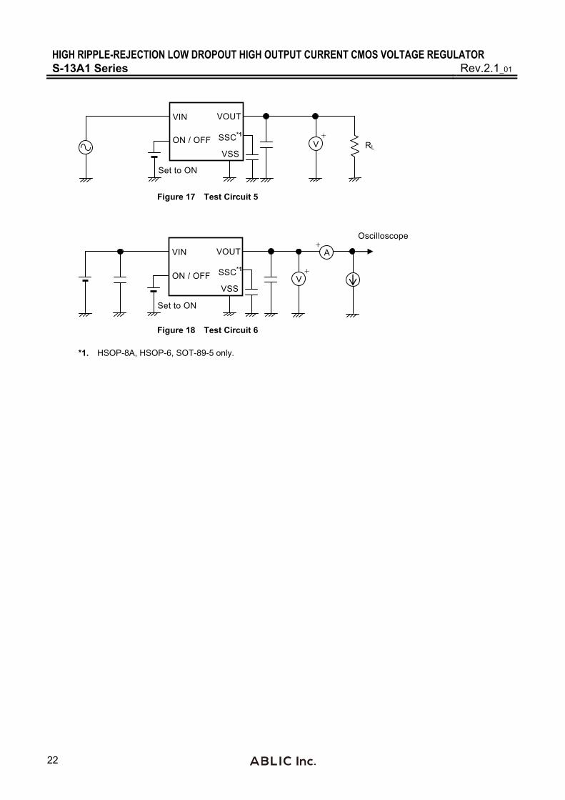
HIGH RIPPLE-REJECTION LOW DROPOUT HIGH OUTPUT CURRENT CMOS VOLTAGE REGULATOR S-13A1 Series Rev.2.1_01
22
VOUTVIN
V ON / OFF
VSSRL
Set to ON
SSC*1
Figure 17 Test Circuit 5
VOUTVIN
VSS
V
A
ON / OFF SSC*1
Oscilloscope
Set to ON
Figure 18 Test Circuit 6
*1. HSOP-8A, HSOP-6, SOT-89-5 only.
HIGH RIPPLE-REJECTION LOW DROPOUT HIGH OUTPUT CURRENT CMOS VOLTAGE REGULATORRev.2.1_01 S-13A1 Series
23
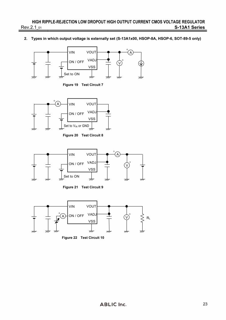
2. Types in which output voltage is externally set (S-13A1x00, HSOP-8A, HSOP-6, SOT-89-5 only)
VOUTVIN
VSS
V
A
ON / OFF
Set to ON
VADJ
Figure 19 Test Circuit 7
VOUTVIN
Set to VIN or GND
A
ON / OFF
VSS
VADJ
Figure 20 Test Circuit 8
Set to ON
VOUTVIN
V
A
ON / OFF
VSS
VADJ
Figure 21 Test Circuit 9
VOUTVIN
V ON / OFF
VSS
A RL
VADJ
Figure 22 Test Circuit 10
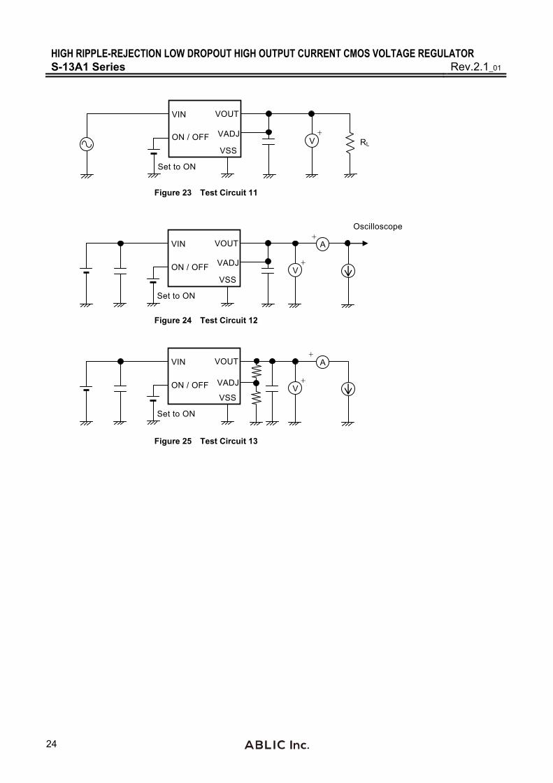
HIGH RIPPLE-REJECTION LOW DROPOUT HIGH OUTPUT CURRENT CMOS VOLTAGE REGULATOR S-13A1 Series Rev.2.1_01
24
VOUTVIN
V ON / OFF
VSSRL
Set to ON
VADJ
Figure 23 Test Circuit 11
VOUTVIN
VSS
V
A
ON / OFF
Oscilloscope
Set to ON
VADJ
Figure 24 Test Circuit 12
VOUTVIN
VSS
V
A
ON / OFF VADJ
Set to ON
Figure 25 Test Circuit 13
HIGH RIPPLE-REJECTION LOW DROPOUT HIGH OUTPUT CURRENT CMOS VOLTAGE REGULATORRev.2.1_01 S-13A1 Series
25
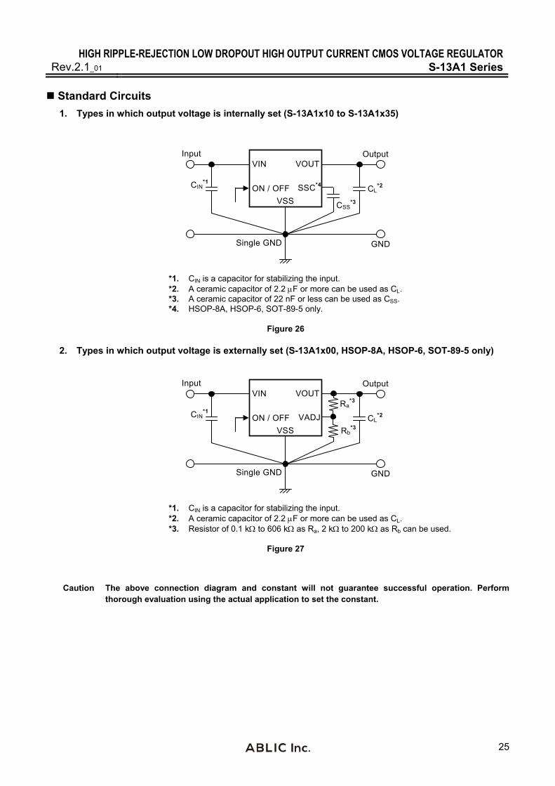
Standard Circuits
1. Types in which output voltage is internally set (S-13A1x10 to S-13A1x35)
CIN*1 CL
*2
Input Output
GNDSingle GND
VOUTVIN
VSS
ON / OFF SSC*4
CSS*3
*1. CIN is a capacitor for stabilizing the input. *2. A ceramic capacitor of 2.2 F or more can be used as CL. *3. A ceramic capacitor of 22 nF or less can be used as CSS. *4. HSOP-8A, HSOP-6, SOT-89-5 only.
Figure 26
2. Types in which output voltage is externally set (S-13A1x00, HSOP-8A, HSOP-6, SOT-89-5 only)
CIN*1 CL
*2
Input Output
GNDSingle GND
VOUTVIN
VSS
ON / OFF
Rb*3
VADJ
Ra*3
*1. CIN is a capacitor for stabilizing the input. *2. A ceramic capacitor of 2.2 F or more can be used as CL. *3. Resistor of 0.1 k to 606 k as Ra, 2 k to 200 k as Rb can be used.
Figure 27
Caution The above connection diagram and constant will not guarantee successful operation. Perform thorough evaluation using the actual application to set the constant.
HIGH RIPPLE-REJECTION LOW DROPOUT HIGH OUTPUT CURRENT CMOS VOLTAGE REGULATOR S-13A1 Series Rev.2.1_01
26
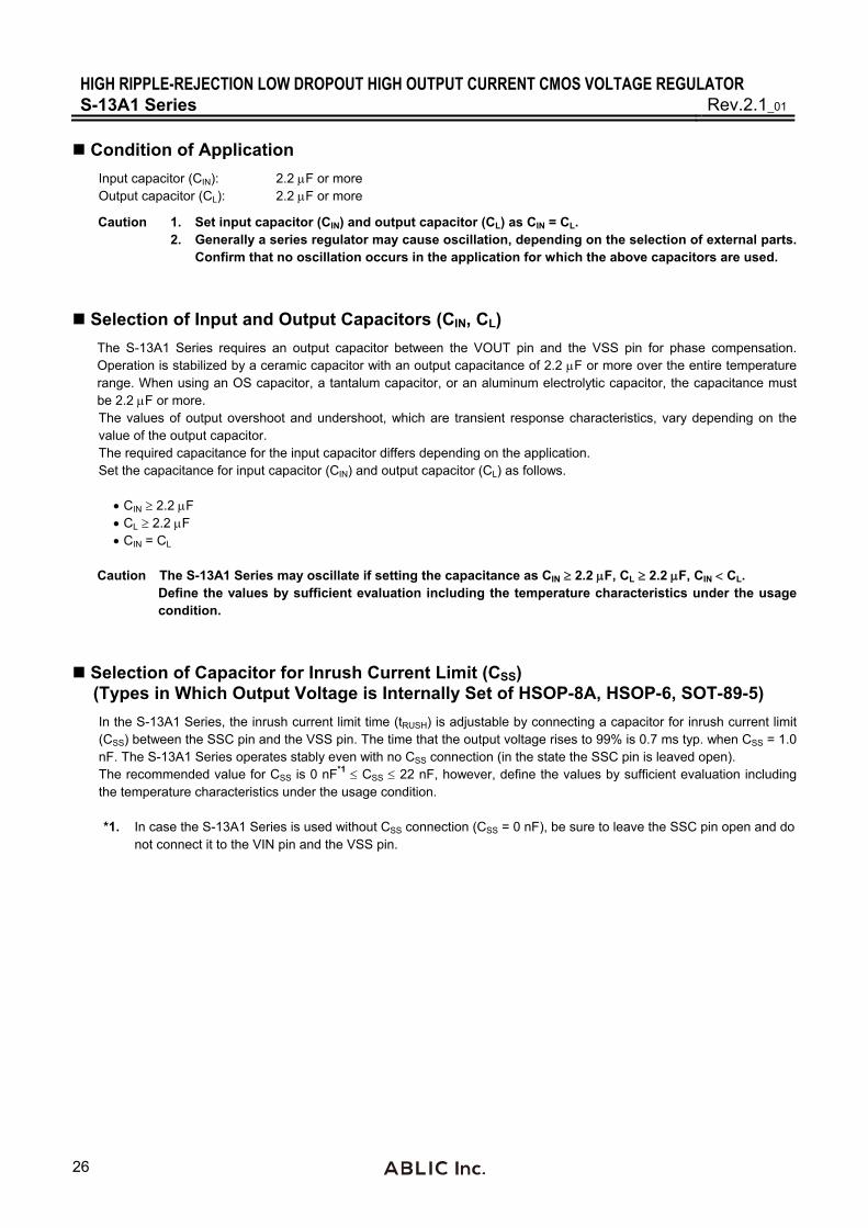
Condition of Application
Input capacitor (CIN): 2.2 F or more Output capacitor (CL): 2.2 F or more
Caution 1. Set input capacitor (CIN) and output capacitor (CL) as CIN = CL. 2. Generally a series regulator may cause oscillation, depending on the selection of external parts. Confirm that no oscillation occurs in the application for which the above capacitors are used.
Selection of Input and Output Capacitors (CIN, CL)
The S-13A1 Series requires an output capacitor between the VOUT pin and the VSS pin for phase compensation. Operation is stabilized by a ceramic capacitor with an output capacitance of 2.2 F or more over the entire temperature range. When using an OS capacitor, a tantalum capacitor, or an aluminum electrolytic capacitor, the capacitance must be 2.2 F or more. The values of output overshoot and undershoot, which are transient response characteristics, vary depending on the value of the output capacitor. The required capacitance for the input capacitor differs depending on the application. Set the capacitance for input capacitor (CIN) and output capacitor (CL) as follows.
CIN 2.2 F CL 2.2 F CIN = CL
Caution The S-13A1 Series may oscillate if setting the capacitance as CIN 2.2 F, CL 2.2 F, CIN CL.
Define the values by sufficient evaluation including the temperature characteristics under the usage condition.
Selection of Capacitor for Inrush Current Limit (CSS) (Types in Which Output Voltage is Internally Set of HSOP-8A, HSOP-6, SOT-89-5)
In the S-13A1 Series, the inrush current limit time (tRUSH) is adjustable by connecting a capacitor for inrush current limit (CSS) between the SSC pin and the VSS pin. The time that the output voltage rises to 99% is 0.7 ms typ. when CSS = 1.0 nF. The S-13A1 Series operates stably even with no CSS connection (in the state the SSC pin is leaved open). The recommended value for CSS is 0 nF*1 CSS 22 nF, however, define the values by sufficient evaluation including the temperature characteristics under the usage condition. *1. In case the S-13A1 Series is used without CSS connection (CSS = 0 nF), be sure to leave the SSC pin open and do
not connect it to the VIN pin and the VSS pin.
HIGH RIPPLE-REJECTION LOW DROPOUT HIGH OUTPUT CURRENT CMOS VOLTAGE REGULATORRev.2.1_01 S-13A1 Series
27
Explanation of Terms
1. Low dropout voltage regulator
This voltage regulator has the low dropout voltage due to its built-in low on-resistance transistor.
2. Output voltage (VOUT)
The accuracy of the output voltage is ensured at 1.0% or 15 mV*1 under the specified conditions of fixed input voltage*2, fixed output current, and fixed temperature. *1. When VOUT 1.5 V: 15 mV, when VOUT 1.5 V: 1.0% *2. Differs depending on the product. Caution If the above conditions change, the output voltage value may vary and exceed the accuracy range
of the output voltage. Refer to " Electrical Characteristics" and " Characteristics (Typical Data)" for details.
3. Line regulation
VOUT1
VINVOUT
Indicates the dependency of the output voltage on the input voltage. That is, the values show how much the output voltage changes due to a change in the input voltage with the output current remaining unchanged.
4. Load regulation (VOUT2)
Indicates the dependency of the output voltage on the output current. That is, the values show how much the output voltage changes due to a change in the output current with the input voltage remaining unchanged.
5. Dropout voltage (Vdrop)
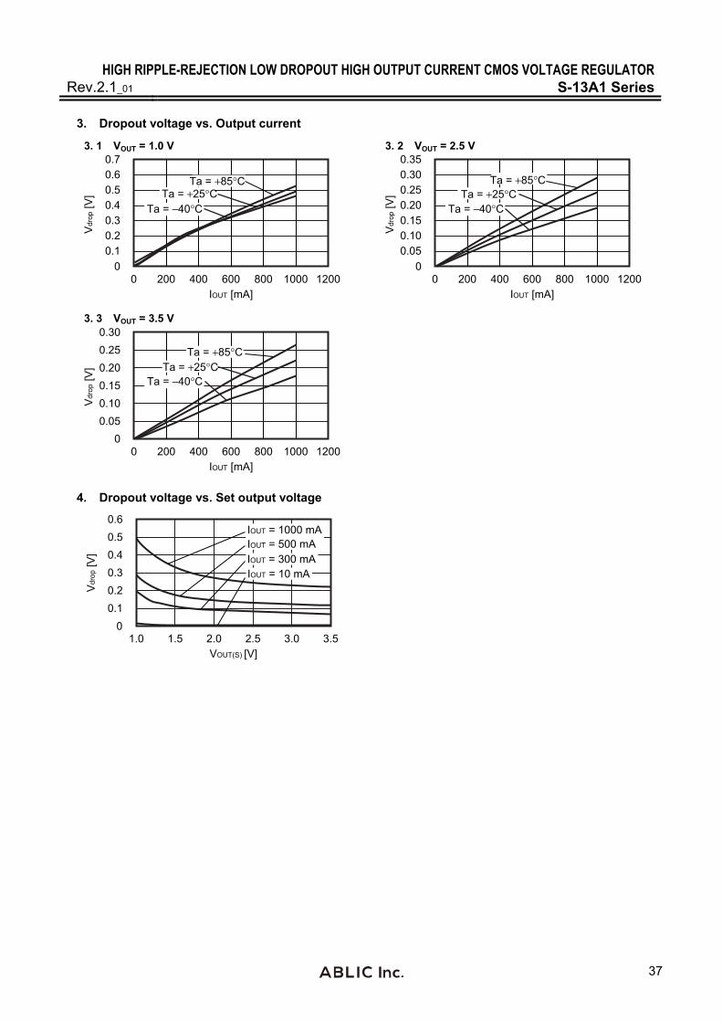
Indicates the difference between input voltage (VIN1) and the output voltage when; decreasing input voltage (VIN) gradually until the output voltage has dropped out to the value of 98% of output voltage (VOUT3), which is at VIN = VOUT(S) 1.0 V.
Vdrop = VIN1 (VOUT3 0.98)
HIGH RIPPLE-REJECTION LOW DROPOUT HIGH OUTPUT CURRENT CMOS VOLTAGE REGULATOR S-13A1 Series Rev.2.1_01
28
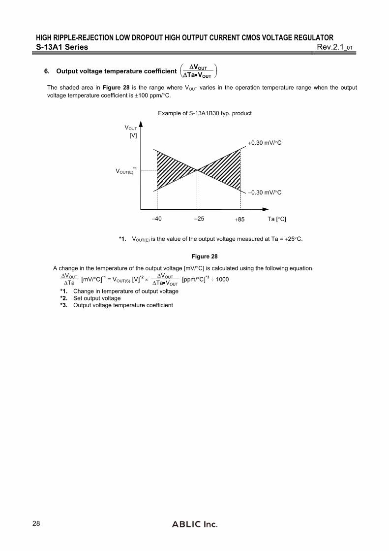
6. Output voltage temperature coefficient
VOUT
TaVOUT
The shaded area in Figure 28 is the range where VOUT varies in the operation temperature range when the output voltage temperature coefficient is 100 ppm/C.
VOUT(E)*1
Example of S-13A1B30 typ. product
40 25
0.30 mV/C
VOUT [V]
*1. VOUT(E) is the value of the output voltage measured at Ta = 25C.
85 Ta [C]
0.30 mV/C
Figure 28
A change in the temperature of the output voltage [mV/°C] is calculated using the following equation. VOUT
Ta [ ]mV/°C *1 = VOUT(S) [ ]V *2
VOUT
TaVOUT [ ]ppm/°C *3 1000
*1. Change in temperature of output voltage *2. Set output voltage *3. Output voltage temperature coefficient
HIGH RIPPLE-REJECTION LOW DROPOUT HIGH OUTPUT CURRENT CMOS VOLTAGE REGULATORRev.2.1_01 S-13A1 Series
29
Operation
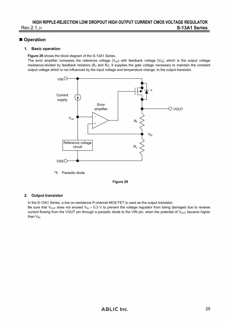
1. Basic operation
Figure 29 shows the block diagram of the S-13A1 Series. The error amplifier compares the reference voltage (Vref) with feedback voltage (Vfb), which is the output voltage resistance-divided by feedback resistors (Rs and Rf). It supplies the gate voltage necessary to maintain the constant output voltage which is not influenced by the input voltage and temperature change, to the output transistor.
*1
*1. Parasitic diode
VSS
Current supply
Vfb
Vref
VIN
VOUT
Rf
Rs
Error amplifier
Reference voltage circuit
Figure 29
2. Output transistor
In the S-13A1 Series, a low on-resistance P-channel MOS FET is used as the output transistor. Be sure that VOUT does not exceed VIN 0.3 V to prevent the voltage regulator from being damaged due to reverse current flowing from the VOUT pin through a parasitic diode to the VIN pin, when the potential of VOUT became higher than VIN.
HIGH RIPPLE-REJECTION LOW DROPOUT HIGH OUTPUT CURRENT CMOS VOLTAGE REGULATOR S-13A1 Series Rev.2.1_01
30
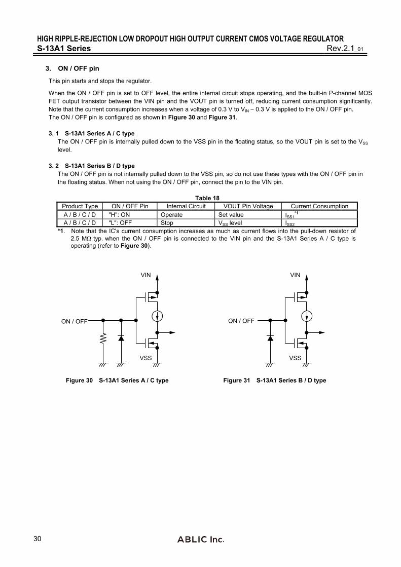
3. ON / OFF pin
This pin starts and stops the regulator.
When the ON / OFF pin is set to OFF level, the entire internal circuit stops operating, and the built-in P-channel MOS FET output transistor between the VIN pin and the VOUT pin is turned off, reducing current consumption significantly. Note that the current consumption increases when a voltage of 0.3 V to VIN 0.3 V is applied to the ON / OFF pin. The ON / OFF pin is configured as shown in Figure 30 and Figure 31. 3. 1 S-13A1 Series A / C type
The ON / OFF pin is internally pulled down to the VSS pin in the floating status, so the VOUT pin is set to the VSS level.
3. 2 S-13A1 Series B / D type
The ON / OFF pin is not internally pulled down to the VSS pin, so do not use these types with the ON / OFF pin in the floating status. When not using the ON / OFF pin, connect the pin to the VIN pin.
Table 18
Product Type ON / OFF Pin Internal Circuit VOUT Pin Voltage Current Consumption
A / B / C / D "H": ON Operate Set value ISS1*1
A / B / C / D "L": OFF Stop VSS level ISS2 *1. Note that the IC's current consumption increases as much as current flows into the pull-down resistor of
2.5 M typ. when the ON / OFF pin is connected to the VIN pin and the S-13A1 Series A / C type is operating (refer to Figure 30).
VSS
VIN
ON / OFF
VSS
VIN
ON / OFF
Figure 30 S-13A1 Series A / C type Figure 31 S-13A1 Series B / D type
HIGH RIPPLE-REJECTION LOW DROPOUT HIGH OUTPUT CURRENT CMOS VOLTAGE REGULATORRev.2.1_01 S-13A1 Series
31
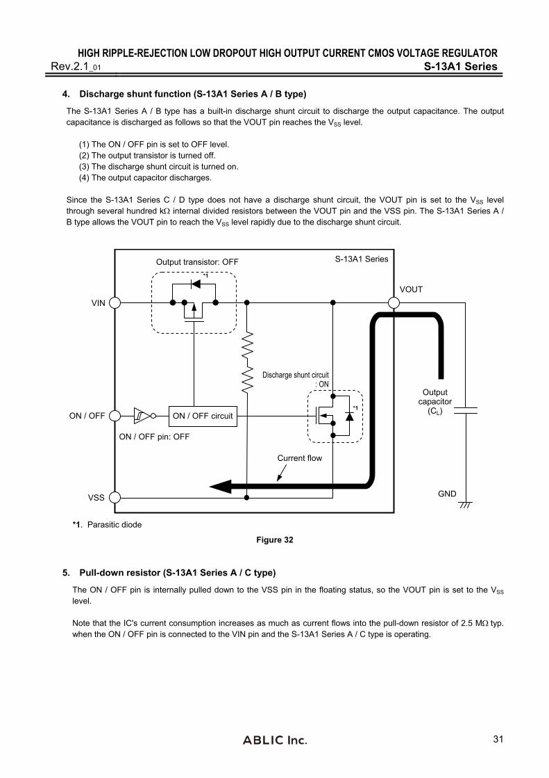
4. Discharge shunt function (S-13A1 Series A / B type)
The S-13A1 Series A / B type has a built-in discharge shunt circuit to discharge the output capacitance. The output capacitance is discharged as follows so that the VOUT pin reaches the VSS level.
(1) The ON / OFF pin is set to OFF level. (2) The output transistor is turned off. (3) The discharge shunt circuit is turned on. (4) The output capacitor discharges.
Since the S-13A1 Series C / D type does not have a discharge shunt circuit, the VOUT pin is set to the VSS level through several hundred k internal divided resistors between the VOUT pin and the VSS pin. The S-13A1 Series A / B type allows the VOUT pin to reach the VSS level rapidly due to the discharge shunt circuit.
Output transistor: OFF
ON / OFF pin: OFF
VIN
ON / OFF
VSS
ON / OFF circuit
Discharge shunt circuit: ON
VOUT
*1
*1. Parasitic diode
Current flow
GND
*1
S-13A1 Series
Output capacitor
(CL)
Figure 32
5. Pull-down resistor (S-13A1 Series A / C type)
The ON / OFF pin is internally pulled down to the VSS pin in the floating status, so the VOUT pin is set to the VSS level. Note that the IC's current consumption increases as much as current flows into the pull-down resistor of 2.5 M typ. when the ON / OFF pin is connected to the VIN pin and the S-13A1 Series A / C type is operating.
HIGH RIPPLE-REJECTION LOW DROPOUT HIGH OUTPUT CURRENT CMOS VOLTAGE REGULATOR S-13A1 Series Rev.2.1_01
32
6. Overcurrent protection circuit
The S-13A1 Series includes an overcurrent protection circuit having the characteristics shown in "1. Output Voltage vs. Output Current (When load current increases) (Ta = 25C)" in " Characteristics (Typical Data)", in order to protect the output transistor against an excessive output current and short circuiting between the VOUT pin and the VSS pin. The current when the output pin is short-circuited (Ishort) is internally set at approx. 200 mA typ., and the normal value is restored for the output voltage, if releasing a short circuit once.
Caution This overcurrent protection circuit does not work as for thermal protection. If this IC long keeps
short circuiting inside, pay attention to the conditions of input voltage and load current so that, under the usage conditions including short circuit, the loss of the IC will not exceed power dissipation of the package.
7. Thermal shutdown circuit
The S-13A1 Series has a thermal shutdown circuit to protect the device from damage due to overheat. When the junction temperature rises to 150C typ., the thermal shutdown circuit operates to stop regulating. When the junction temperature drops to 120C typ., the thermal shutdown circuit is released to restart regulating. Due to self-heating of the S-13A1 Series, if the thermal shutdown circuit starts operating, it stops regulating so that the output voltage drops. When regulation stops, the S-13A1 does not itself generate heat so that the IC’s temperature drops. When the temperature drops, the thermal shutdown circuit is released to restart regulating, thus the S-13A1 Series generates heat again. Repeating this procedure makes waveform of the output voltage pulse-like form. Stop or restart of regulation continues unless decreasing either or both of the input voltage and the output voltage in order to reduce the internal power consumption, or decreasing the ambient temperature.
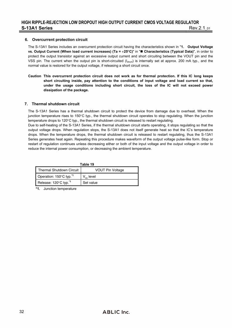
Table 19
Thermal Shutdown Circuit VOUT Pin Voltage
Operation: 150C typ.*1 VSS level
Release: 120C typ.*1 Set value
*1. Junction temperature
HIGH RIPPLE-REJECTION LOW DROPOUT HIGH OUTPUT CURRENT CMOS VOLTAGE REGULATORRev.2.1_01 S-13A1 Series
33
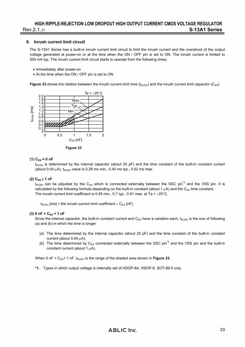
8. Inrush current limit circuit
The S-13A1 Series has a built-in inrush current limit circuit to limit the inrush current and the overshoot of the output voltage generated at power-on or at the time when the ON / OFF pin is set to ON. The inrush current is limited to 500 mA typ. The inrush current limit circuit starts to operate from the following times. Immediately after power-on At the time when the ON / OFF pin is set to ON
Figure 33 shows the relation between the inrush current limit time (tRUSH) and the inrush current limit capacitor (CSS).
Typ.
Max.
Min.
2.0
1.6
1.2
0
t RU
SH [
ms]
0.8
0.2
0 0.5 1 1.5 2CSS [nF]
0.40.6
1.8
1.4
1.0
Figure 33
Ta = 25°C
(1) CSS = 0 nF
tRUSH is determined by the internal capacitor (about 20 pF) and the time constant of the built-in constant current (about 0.04 A). tRUSH value is 0.28 ms min., 0.40 ms typ., 0.52 ms max.
(2) CSS 1 nF
tRUSH can be adjusted by the CSS which is connected externally between the SSC pin*1 and the VSS pin. It is calculated by the following formula depending on the built-in constant (about 1 A) and the CSS time constant. The inrush current limit coefficient is 0.49 min., 0.7 typ., 0.91 max. at Ta = 25C.
tRUSH [ms] = the inrush current limit coefficient CSS [nF]
(3) 0 nF < CSS < 1 nF
Since the internal capacitor, the built-in constant current and CSS have a variation each, tRUSH is the one of following (a) and (b) in which the time is longer.
(a) The time determined by the internal capacitor (about 20 pF) and the time constant of the built-in constant current (about 0.04 A).
(b) The time determined by CSS connected externally between the SSC pin*1 and the VSS pin and the built-in constant current (about 1 A).
When 0 nF < CSS< 1 nF, tRUSH is the range of the shaded area shown in Figure 33. *1. Types in which output voltage is internally set of HSOP-8A, HSOP-6, SOT-89-5 only.
HIGH RIPPLE-REJECTION LOW DROPOUT HIGH OUTPUT CURRENT CMOS VOLTAGE REGULATOR S-13A1 Series Rev.2.1_01
34
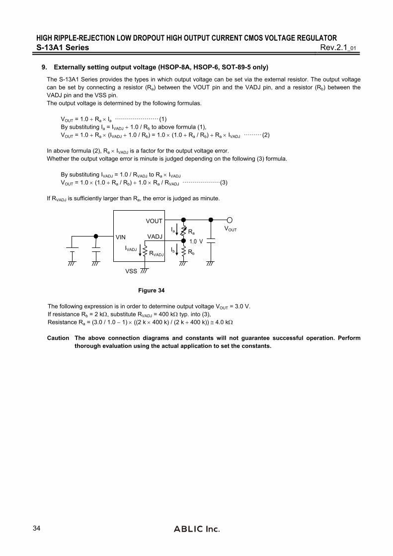
9. Externally setting output voltage (HSOP-8A, HSOP-6, SOT-89-5 only)
The S-13A1 Series provides the types in which output voltage can be set via the external resistor. The output voltage can be set by connecting a resistor (Ra) between the VOUT pin and the VADJ pin, and a resistor (Rb) between the VADJ pin and the VSS pin. The output voltage is determined by the following formulas.
VOUT = 1.0 Ra la ······················ (1) By substituting Ia = IVADJ 1.0 / Rb to above formula (1), VOUT = 1.0 Ra (IVADJ 1.0 / Rb) = 1.0 (1.0 Ra / Rb) Ra IVADJ ········· (2)
In above formula (2), Ra IVADJ is a factor for the output voltage error. Whether the output voltage error is minute is judged depending on the following (3) formula.
By substituting IVADJ = 1.0 / RVADJ to Ra IVADJ VOUT = 1.0 (1.0 Ra / Rb) 1.0 Ra / RVADJ ··················· (3)
If RVADJ is sufficiently larger than Ra, the error is judged as minute.
VSS
VOUT
VIN VADJ
VOUTRa
Rb
Ia
IbRVADJ
IVADJ 1.0 V
Figure 34
The following expression is in order to determine output voltage VOUT = 3.0 V. If resistance Rb = 2 k, substitute RVADJ = 400 k typ. into (3), Resistance Ra = (3.0 / 1.0 1) ((2 k 400 k) / (2 k 400 k)) 4.0 k Caution The above connection diagrams and constants will not guarantee successful operation. Perform
thorough evaluation using the actual application to set the constants.
HIGH RIPPLE-REJECTION LOW DROPOUT HIGH OUTPUT CURRENT CMOS VOLTAGE REGULATORRev.2.1_01 S-13A1 Series
35
Precautions
Wiring patterns for the VIN pin, the VOUT pin and GND should be designed so that the impedance is low. When mounting an output capacitor between the VOUT pin and the VSS pin (CL), a capacitor for stabilizing the input between the VIN pin and the VSS pin (CIN), and a capacitor for limiting the inrush current between the SSC pin and the VSS pin (CSS), the distance from the capacitors to these pins should be as short as possible.
Note that generally the output voltage may increase when a series regulator is used at low load current (1.0 mA or less).
Note that generally the output voltage may increase due to the leakage current from an output driver when a series regulator is used at high temperature.
Note that the output voltage may increase due to the leakage current from an output driver even if the ON / OFF pin is at OFF level when a series regulator is used at high temperature.
Generally a series regulator may cause oscillation, depending on the selection of external parts. The following conditions are recommended for the S-13A1 Series. However, be sure to perform sufficient evaluation under the actual usage conditions for selection, including evaluation of temperature characteristics. Refer to "6. Example of equivalent series resistance vs. Output current characteristics (Ta = 25C)" in " Reference Data" for the equivalent series resistance (RESR) of the output capacitor.
Input capacitor (CIN): 2.2 F or more Output capacitor (CL): 2.2 F or more The voltage regulator may oscillate when the impedance of the power supply is high and the input capacitance is small
or an input capacitor is not connected.
If the output capacitance is small, power supply's fluctuation and the characteristics of load fluctuation become worse. Sufficiently evaluate the output voltage's fluctuation with the actual device.
Overshoot may occur in the output voltage momentarily if the voltage is rapidly raised at power-on or when the power supply fluctuates. Sufficiently evaluate the output voltage at power-on with the actual device.
The application conditions for the input voltage, the output voltage, and the load current should not exceed the power dissipation.
Do not apply an electrostatic discharge to this IC that exceeds the performance ratings of the built-in electrostatic protection circuit.
In determining the output current, attention should be paid to the output current value specified in Table 16 and Table 17 in " Electrical Characteristics" and footnote *5 of the table.
ABLIC Inc. claims no responsibility for any disputes arising out of or in connection with any infringement by products including this IC of patents owned by a third party.
HIGH RIPPLE-REJECTION LOW DROPOUT HIGH OUTPUT CURRENT CMOS VOLTAGE REGULATOR S-13A1 Series Rev.2.1_01
36
Characteristics (Typical Data)
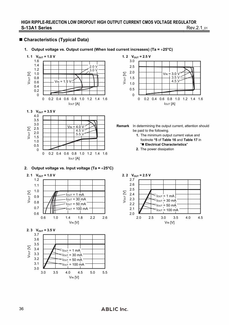
1. Output voltage vs. Output current (When load current increases) (Ta = 25°C)
1. 1 VOUT = 1.0 V 1. 2 VOUT = 2.5 V
0
VO
UT
[V]
0
IOUT [A]
1.61.41.21.00.80.60.40.2
1.61.41.21.00.80.60.40.2
VIN = 1.5 V
2.0 V3.0 V
VO
UT
[V]
0
3.02.52.01.51.00.5
VIN = 3.0 V3.5 V4.5 V
0IOUT [A]
1.61.41.21.00.80.60.40.2
1. 3 VOUT = 3.5 V
VO
UT
[V]
0
4.03.53.02.52.01.51.00.5
VIN = 4.0 V4.5 V5.5 V
0IOUT [A]
1.61.41.21.00.80.60.40.2
Remark In determining the output current, attention should be paid to the following.
1. The minimum output current value and footnote *5 of Table 16 and Table 17 in " Electrical Characteristics"
2. The power dissipation
2. Output voltage vs. Input voltage (Ta = 25°C)
2. 1 VOUT = 1.0 V 2. 2 VOUT = 2.5 V
0.6
VO
UT
[V]
0.6
VIN [V]
1.2
2.62.21.81.41.0
1.11.00.90.80.7
IOUT = 1 mA
IOUT = 50 mAIOUT = 30 mA
IOUT = 100 mA
2.0
VO
UT
[V]
2.0
VIN [V]
2.72.62.52.42.32.22.1
4.54.03.53.02.5
IOUT = 1 mA
IOUT = 50 mAIOUT = 30 mA
IOUT = 100 mA
2. 3 VOUT = 3.5 V
3.0
VO
UT
[V]
3.0
VIN [V]
3.73.63.53.43.33.23.1
5.55.04.54.03.5
IOUT = 1 mA
IOUT = 50 mAIOUT = 30 mA
IOUT = 100 mA
HIGH RIPPLE-REJECTION LOW DROPOUT HIGH OUTPUT CURRENT CMOS VOLTAGE REGULATORRev.2.1_01 S-13A1 Series
37
3. Dropout voltage vs. Output current
3. 1 VOUT = 1.0 V 3. 2 VOUT = 2.5 V
0
Vdr
op [V
]
0
IOUT [mA]
0.7
1200
0.60.50.40.30.20.1
400 800600200 1000
Ta = +25°CTa = +85°C
Ta = −40°C
0
Vdr
op [V
]
0
IOUT [mA]
0.35
1200
0.300.250.200.150.100.05
400 800600200 1000
Ta = +25°CTa = +85°C
Ta = −40°C
3. 3 VOUT = 3.5 V
0
Vdr
op [V
]
0
IOUT [mA]1200400 800600200 1000
0.300.250.200.150.100.05
Ta = +25°CTa = +85°C
Ta = −40°C
4. Dropout voltage vs. Set output voltage
1.0
Vdr
op [V
]
0
VOUT(S) [V]
0.6
3.53.02.52.01.5
0.50.40.30.20.1
IOUT = 1000 mA
IOUT = 300 mAIOUT = 500 mA
IOUT = 10 mA
HIGH RIPPLE-REJECTION LOW DROPOUT HIGH OUTPUT CURRENT CMOS VOLTAGE REGULATOR S-13A1 Series Rev.2.1_01
38
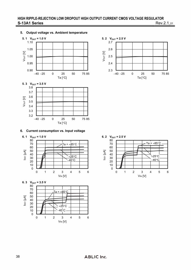
5. Output voltage vs. Ambient temperature
5. 1 VOUT = 1.0 V 5. 2 VOUT = 2.5 V
−40 0 25 50 75
VO
UT
[V]
1.10
1.00
0.95
0.90
Ta [°C]
1.05
−25 85 −40 0 25 50 75
VO
UT
[V]
2.7
2.5
2.4
2.3
Ta [°C]
2.6
−25 85
5. 3 VOUT = 3.5 V
−40 0 25 50 75
VO
UT
[V]
3.8
3.2
Ta [°C]−25 85
3.73.63.53.43.3
6. Current consumption vs. Input voltage
6. 1 VOUT = 1.0 V 6. 2 VOUT = 2.5 V
0 2 40
31
80
5 6
70605040302010
ISS
1 [μA
]
VIN [V]
+25°C−40°C
Ta = +85°C
0 2 40
31
80
5 6
70605040302010
ISS
1 [μA
]
VIN [V]
+25°C−40°C
Ta = +85°C
6. 3 VOUT = 3.5 V
0 2 40
31
80
5 6
70605040302010
ISS
1 [μA
]
VIN [V]
+25°C−40°C
Ta = +85°C
HIGH RIPPLE-REJECTION LOW DROPOUT HIGH OUTPUT CURRENT CMOS VOLTAGE REGULATORRev.2.1_01 S-13A1 Series
39
7. Ripple rejection (Ta = 25°C)
7. 1 VOUT = 1.0 V 7. 2 VOUT = 2.5 V
VIN = 2.0 V, CL = 2.2 F
10 100 1k 10k 100k
Rip
ple
Rej
ectio
n [d
B]
0
Frequency [Hz]1M
100908070605040302010
IOUT = 1 mA
IOUT = 100 mAIOUT = 30 mA
VIN = 3.5 V, CL = 2.2 F
10 100 1k 10k 100k
Rip
ple
Rej
ectio
n [d
B]
0
Frequency [Hz]1M
100908070605040302010
IOUT = 1 mA
IOUT = 100 mAIOUT = 30 mA
7. 3 VOUT = 3.5 V
VIN = 4.5 V, CL = 2.2 F
10 100 1k 10k 100k
Rip
ple
Rej
ectio
n [d
B]
0
Frequency [Hz]1M
100908070605040302010
IOUT = 1 mA
IOUT = 100 mAIOUT = 30 mA
HIGH RIPPLE-REJECTION LOW DROPOUT HIGH OUTPUT CURRENT CMOS VOLTAGE REGULATOR S-13A1 Series Rev.2.1_01
40
Reference Data
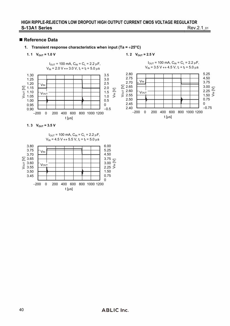
1. Transient response characteristics when input (Ta = 25°C)
1. 1 VOUT = 1.0 V 1. 2 VOUT = 2.5 V
IOUT = 100 mA, CIN = CL = 2.2 F, VIN = 2.0 V 3.0 V, tr = tf = 5.0 s
VO
UT
[V]
1.301.251.201.151.101.051.000.950.90
t [μs]V
IN [V
]
3.5
2.52.01.5
−0.500.51.0
3.0
8000 200 400 600 1000 1200−200
VOUT
VIN
IOUT = 100 mA, CIN = CL = 2.2 F, VIN = 3.5 V 4.5 V, tr = tf = 5.0 s
VO
UT
[V]
2.802.752.702.652.602.552.502.452.40
t [μs]
VIN
[V]
5.25
3.753.002.25
−0.7500.751.50
4.50
8000 200 400 600 1000 1200−200
VOUT
VIN
1. 3 VOUT = 3.5 V
IOUT = 100 mA, CIN = CL = 2.2 F, VIN = 4.5 V 5.5 V, tr = tf = 5.0 s
VO
UT
[V]
3.803.753.703.653.603.553.503.45
t [μs]
VIN
[V]
8000 200 400 600 1000 1200−200
6.00
4.503.753.00
00.751.502.25
5.25
VOUT
VIN
HIGH RIPPLE-REJECTION LOW DROPOUT HIGH OUTPUT CURRENT CMOS VOLTAGE REGULATORRev.2.1_01 S-13A1 Series
41
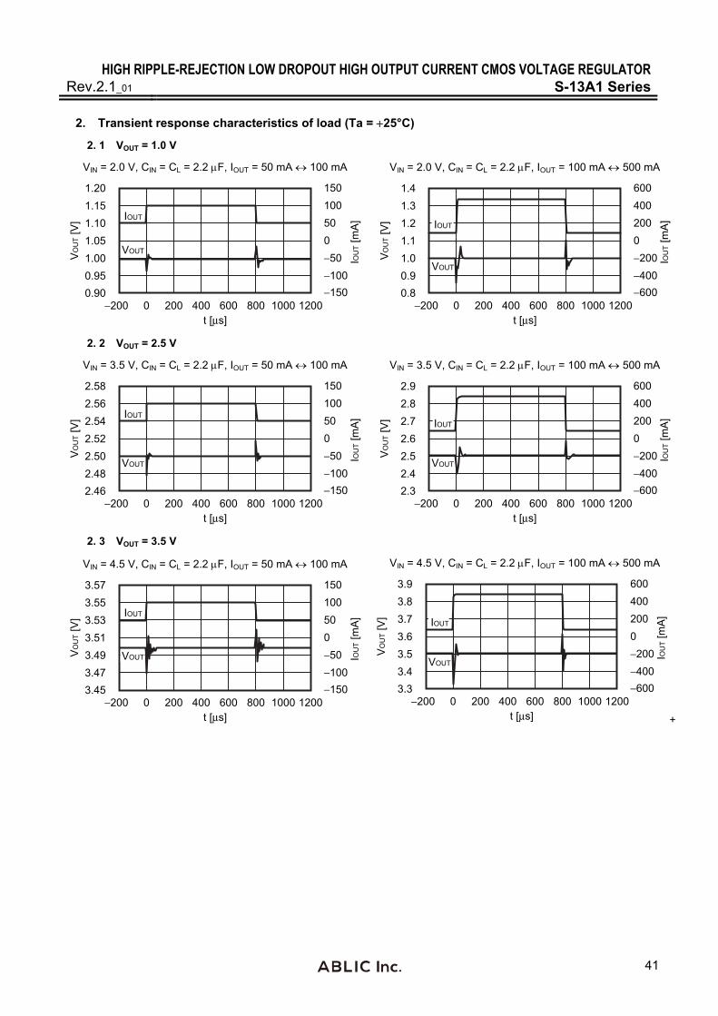
2. Transient response characteristics of load (Ta = 25°C)
2. 1 VOUT = 1.0 V
VIN = 2.0 V, CIN = CL = 2.2 F, IOUT = 50 mA 100 mA
VO
UT
[V]
t [μs]
IOU
T [m
A]
120010008006004002000−200
1.201.151.101.051.000.950.90
150100500−50−100−150
IOUT
VOUT
VIN = 2.0 V, CIN = CL = 2.2 F, IOUT = 100 mA 500 mA
VO
UT
[V]
t [μs]
IOU
T [m
A]
120010008006004002000−200
1.41.31.21.11.00.90.8
6004002000−200−400−600
IOUT
VOUT
2. 2 VOUT = 2.5 V
VIN = 3.5 V, CIN = CL = 2.2 F, IOUT = 50 mA 100 mA
VO
UT
[V]
2.582.562.542.522.502.482.46
t [μs]
IOU
T [m
A]
150100500−50−100−150
120010008006004002000−200
IOUT
VOUT
VIN = 3.5 V, CIN = CL = 2.2 F, IOUT = 100 mA 500 mA
VO
UT
[V]
t [μs]
IOU
T [m
A]
120010008006004002000−200
2.92.82.72.62.52.42.3
6004002000−200−400−600
IOUT
VOUT
2. 3 VOUT = 3.5 V
VIN = 4.5 V, CIN = CL = 2.2 F, IOUT = 50 mA 100 mA
VO
UT
[V]
t [μs]
IOU
T [m
A]
120010008006004002000−200
3.573.553.533.513.493.473.45
150100500−50−100−150
IOUT
VOUT
VIN = 4.5 V, CIN = CL = 2.2 F, IOUT = 100 mA 500 mA
VO
UT
[V]
t [μs]
IOU
T [m
A]
120010008006004002000−200
3.93.83.73.63.53.43.3
6004002000−200−400−600
IOUT
VOUT
+
HIGH RIPPLE-REJECTION LOW DROPOUT HIGH OUTPUT CURRENT CMOS VOLTAGE REGULATOR S-13A1 Series Rev.2.1_01
42
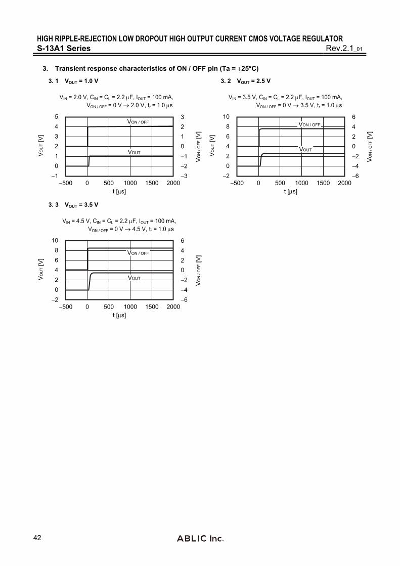
3. Transient response characteristics of ON / OFF pin (Ta = 25°C)
3. 1 VOUT = 1.0 V 3. 2 VOUT = 2.5 V
VIN = 2.0 V, CIN = CL = 2.2 F, IOUT = 100 mA, VON / OFF = 0 V 2.0 V, tr = 1.0 s
−500−1
5
2000
43210
VO
UT
[V]
t [μs]V
ON
/ O
FF [V
]
3210−1−2−3
150010005000
VON / OFF
VOUT
VIN = 3.5 V, CIN = CL = 2.2 F, IOUT = 100 mA, VON / OFF = 0 V 3.5 V, tr = 1.0 s
−500−2
10
2000
86420
VO
UT
[V]
t [μs]
VO
N /
OFF
[V]
6420
−6−4−2
150010005000
VON / OFF
VOUT
3. 3 VOUT = 3.5 V
VIN = 4.5 V, CIN = CL = 2.2 F, IOUT = 100 mA, VON / OFF = 0 V 4.5 V, tr = 1.0 s
−500−2
10
2000
86420
VO
UT
[V]
t [μs]
VO
N /
OFF
[V]
6420
−6−4−2
150010005000
VON / OFF
VOUT
HIGH RIPPLE-REJECTION LOW DROPOUT HIGH OUTPUT CURRENT CMOS VOLTAGE REGULATORRev.2.1_01 S-13A1 Series
43
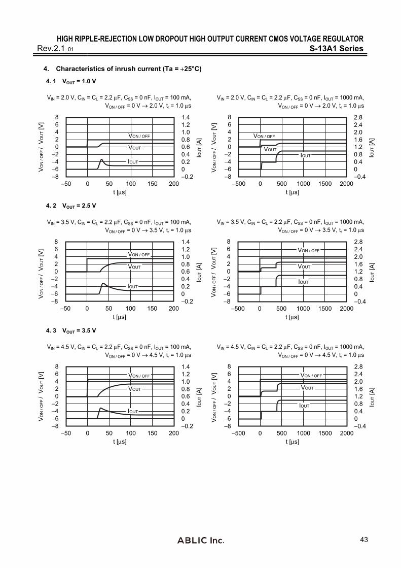
4. Characteristics of inrush current (Ta = 25°C)
4. 1 VOUT = 1.0 V
VIN = 2.0 V, CIN = CL = 2.2 F, CSS = 0 nF, IOUT = 100 mA, VON / OFF = 0 V 2.0 V, tr = 1.0 s
−50−8
8
200
6420
−2−4−6
t [μs]
1.41.21.00.80.6
−0.200.20.4
150100500
IOU
T [A
]
VO
N /
OFF
/ V
OU
T [V
]
VON / OFF
VOUT
IOUT
VIN = 2.0 V, CIN = CL = 2.2 F, CSS = 0 nF, IOUT = 1000 mA, VON / OFF = 0 V 2.0 V, tr = 1.0 s
−500−8
8
2000
6420
−2−4−6
t [μs]
2.82.42.01.61.2
−0.400.40.8
150010005000
IOU
T [A
]
VOUTIOUT
VO
N /
OFF
/ V
OU
T [V
]
VON / OFF
4. 2 VOUT = 2.5 V
VIN = 3.5 V, CIN = CL = 2.2 F, CSS = 0 nF, IOUT = 100 mA, VON / OFF = 0 V 3.5 V, tr = 1.0 s
−50−8
8
200
6420
−2−4−6
t [μs]
1.41.21.00.80.6
−0.200.20.4
150100500
IOU
T [A
]
VON / OFF
VOUT
IOUT
VO
N /
OFF
/ V
OU
T [V
]
VIN = 3.5 V, CIN = CL = 2.2 F, CSS = 0 nF, IOUT = 1000 mA, VON / OFF = 0 V 3.5 V, tr = 1.0 s
−500−8
8
2000
6420
−2−4−6
t [μs]
2.82.42.01.61.2
−0.400.40.8
150010005000
IOU
T [A
]
VON / OFF
VOUT
IOUT
VO
N /
OFF
/ V
OU
T [V
]
4. 3 VOUT = 3.5 V
VIN = 4.5 V, CIN = CL = 2.2 F, CSS = 0 nF, IOUT = 100 mA, VON / OFF = 0 V 4.5 V, tr = 1.0 s
−50−8
8
200
6420
−2−4−6
t [μs]
1.41.21.00.80.6
−0.200.20.4
150100500
IOU
T [A
]
VO
N /
OFF
/ V
OU
T [V
]
VON / OFF
VOUT
IOUT
VIN = 4.5 V, CIN = CL = 2.2 F, CSS = 0 nF, IOUT = 1000 mA, VON / OFF = 0 V 4.5 V, tr = 1.0 s
−500−8
8
2000
6420
−2−4−6
t [μs]
2.82.42.01.61.2
−0.400.40.8
150010005000
IOU
T [A
] VON / OFF
VOUT
IOUT
VO
N /
OFF
/ V
OU
T [V
]
HIGH RIPPLE-REJECTION LOW DROPOUT HIGH OUTPUT CURRENT CMOS VOLTAGE REGULATOR S-13A1 Series Rev.2.1_01
44
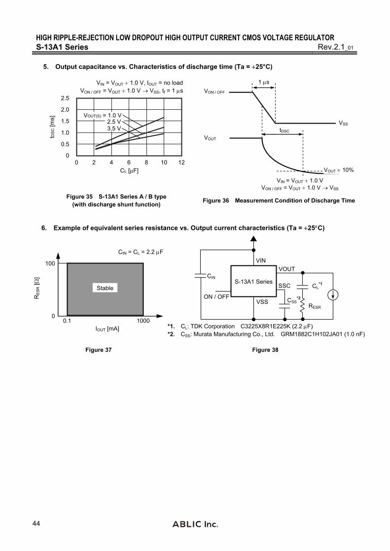
5. Output capacitance vs. Characteristics of discharge time (Ta = 25°C)
VIN = VOUT 1.0 V, IOUT = no load VON / OFF = VOUT 1.0 V VSS, tf = 1 s
tDS
C [m
s]
0
CL [μF]2 4 6 8
2.5
0 10 12
2.0
1.5
1.0
0.5
VOUT(S) = 1.0 V
3.5 V2.5 V
VOUT
VON / OFF
1 s
tDSC
VOUT 10%
VSS
VIN = VOUT 1.0 V VON / OFF = VOUT 1.0 V VSS
Figure 35 S-13A1 Series A / B type (with discharge shunt function)
Figure 36 Measurement Condition of Discharge Time
6. Example of equivalent series resistance vs. Output current characteristics (Ta = 25C)
100
0.1 1000 IOUT [mA]
RE
SR [
]
CIN = CL = 2.2 F
0
Stable
CIN
VIN
VSS
S-13A1 Series
VOUT
ON / OFF
CL*1
RESR
SSC
CSS*2
*1. CL: TDK Corporation C3225X8R1E225K (2.2 F) *2. CSS: Murata Manufacturing Co., Ltd. GRM1882C1H102JA01 (1.0 nF)
Figure 37 Figure 38
HIGH RIPPLE-REJECTION LOW DROPOUT HIGH OUTPUT CURRENT CMOS VOLTAGE REGULATORRev.2.1_01 S-13A1 Series
45
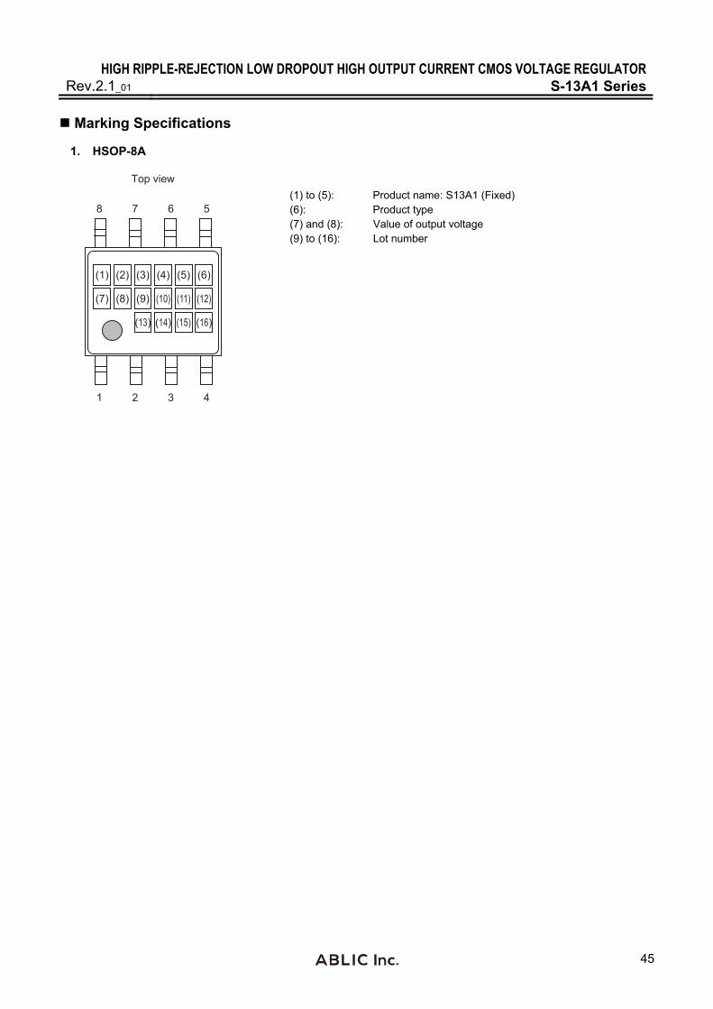
Marking Specifications
1. HSOP-8A
(1) (2) (3) (4)
(7) (8) (9) (10)
(13) (14)
(5) (6)
(11) (12)
(15) (16)
Top view
8 67 5
1 32 4
(1) to (5): Product name: S13A1 (Fixed) (6): Product type (7) and (8): Value of output voltage (9) to (16): Lot number
HIGH RIPPLE-REJECTION LOW DROPOUT HIGH OUTPUT CURRENT CMOS VOLTAGE REGULATOR S-13A1 Series Rev.2.1_01
46
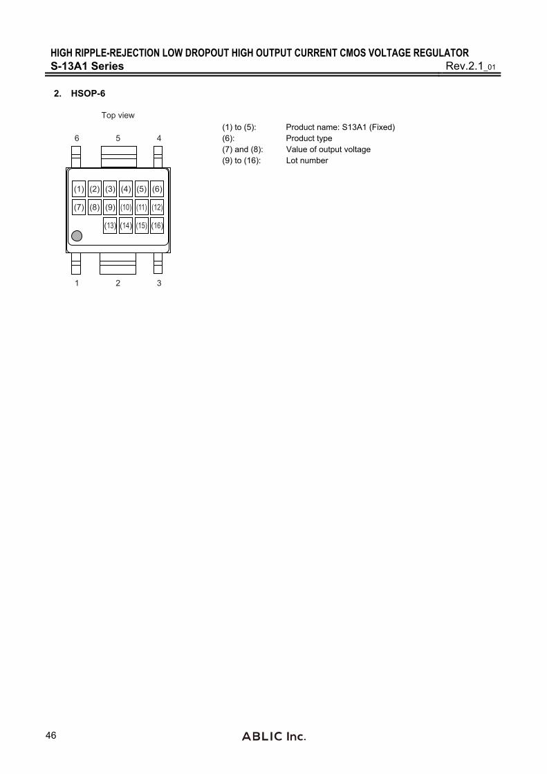
2. HSOP-6
(1) (2) (3) (4)
(7) (8) (9) (10)
(13) (14)
(5) (6)
(11) (12)
(15) (16)
Top view
6 5 4
1 2 3
(1) to (5): Product name: S13A1 (Fixed) (6): Product type (7) and (8): Value of output voltage (9) to (16): Lot number
HIGH RIPPLE-REJECTION LOW DROPOUT HIGH OUTPUT CURRENT CMOS VOLTAGE REGULATORRev.2.1_01 S-13A1 Series
47
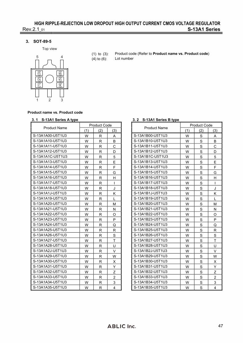
3. SOT-89-5 (1
)(2
)(3
)
(4)
(5)
(6)
1 2 3
45
Top view
(1) to (3): Product code (Refer to Product name vs. Product code)
(4) to (6): Lot number
Product name vs. Product code
3. 1 S-13A1 Series A type 3. 2 S-13A1 Series B type
Product Name Product Code
Product Name Product Code
(1) (2) (3) (1) (2) (3) S-13A1A00-U5T1U3 W R A S-13A1B00-U5T1U3 W S A S-13A1A10-U5T1U3 W R B S-13A1B10-U5T1U3 W S B S-13A1A11-U5T1U3 W R C S-13A1B11-U5T1U3 W S C S-13A1A12-U5T1U3 W R D S-13A1B12-U5T1U3 W S D S-13A1A1C-U5T1U3 W R 5 S-13A1B1C-U5T1U3 W S 5 S-13A1A13-U5T1U3 W R E S-13A1B13-U5T1U3 W S E S-13A1A14-U5T1U3 W R F S-13A1B14-U5T1U3 W S F S-13A1A15-U5T1U3 W R G S-13A1B15-U5T1U3 W S G S-13A1A16-U5T1U3 W R H S-13A1B16-U5T1U3 W S H S-13A1A17-U5T1U3 W R I S-13A1B17-U5T1U3 W S I S-13A1A18-U5T1U3 W R J S-13A1B18-U5T1U3 W S J S-13A1A1J-U5T1U3 W R K S-13A1B1J-U5T1U3 W S K S-13A1A19-U5T1U3 W R L S-13A1B19-U5T1U3 W S L S-13A1A20-U5T1U3 W R M S-13A1B20-U5T1U3 W S M S-13A1A21-U5T1U3 W R N S-13A1B21-U5T1U3 W S N S-13A1A22-U5T1U3 W R O S-13A1B22-U5T1U3 W S O S-13A1A23-U5T1U3 W R P S-13A1B23-U5T1U3 W S P S-13A1A24-U5T1U3 W R Q S-13A1B24-U5T1U3 W S Q S-13A1A25-U5T1U3 W R R S-13A1B25-U5T1U3 W S R S-13A1A26-U5T1U3 W R S S-13A1B26-U5T1U3 W S S S-13A1A27-U5T1U3 W R T S-13A1B27-U5T1U3 W S T S-13A1A28-U5T1U3 W R U S-13A1B28-U5T1U3 W S U S-13A1A2J-U5T1U3 W R V S-13A1B2J-U5T1U3 W S V S-13A1A29-U5T1U3 W R W S-13A1B29-U5T1U3 W S W S-13A1A30-U5T1U3 W R X S-13A1B30-U5T1U3 W S X S-13A1A31-U5T1U3 W R Y S-13A1B31-U5T1U3 W S Y S-13A1A32-U5T1U3 W R Z S-13A1B32-U5T1U3 W S Z S-13A1A33-U5T1U3 W R 2 S-13A1B33-U5T1U3 W S 2 S-13A1A34-U5T1U3 W R 3 S-13A1B34-U5T1U3 W S 3 S-13A1A35-U5T1U3 W R 4 S-13A1B35-U5T1U3 W S 4

HIGH RIPPLE-REJECTION LOW DROPOUT HIGH OUTPUT CURRENT CMOS VOLTAGE REGULATOR S-13A1 Series Rev.2.1_01
48
3. 3 S-13A1 Series C type 3. 4 S-13A1 Series D type
Product Name Product Code
Product Name Product Code
(1) (2) (3) (1) (2) (3) S-13A1C00-U5T1U3 W T A S-13A1D00-U5T1U3 W U A S-13A1C10-U5T1U3 W T B S-13A1D10-U5T1U3 W U B S-13A1C11-U5T1U3 W T C S-13A1D11-U5T1U3 W U C S-13A1C12-U5T1U3 W T D S-13A1D12-U5T1U3 W U D S-13A1C1C-U5T1U3 W T 5 S-13A1D1C-U5T1U3 W U 5 S-13A1C13-U5T1U3 W T E S-13A1D13-U5T1U3 W U E S-13A1C14-U5T1U3 W T F S-13A1D14-U5T1U3 W U F S-13A1C15-U5T1U3 W T G S-13A1D15-U5T1U3 W U G S-13A1C16-U5T1U3 W T H S-13A1D16-U5T1U3 W U H S-13A1C17-U5T1U3 W T I S-13A1D17-U5T1U3 W U I S-13A1C18-U5T1U3 W T J S-13A1D18-U5T1U3 W U J S-13A1C1J-U5T1U3 W T K S-13A1D1J-U5T1U3 W U K S-13A1C19-U5T1U3 W T L S-13A1D19-U5T1U3 W U L S-13A1C20-U5T1U3 W T M S-13A1D20-U5T1U3 W U M S-13A1C21-U5T1U3 W T N S-13A1D21-U5T1U3 W U N S-13A1C22-U5T1U3 W T O S-13A1D22-U5T1U3 W U O S-13A1C23-U5T1U3 W T P S-13A1D23-U5T1U3 W U P S-13A1C24-U5T1U3 W T Q S-13A1D24-U5T1U3 W U Q S-13A1C25-U5T1U3 W T R S-13A1D25-U5T1U3 W U R S-13A1C26-U5T1U3 W T S S-13A1D26-U5T1U3 W U S S-13A1C27-U5T1U3 W T T S-13A1D27-U5T1U3 W U T S-13A1C28-U5T1U3 W T U S-13A1D28-U5T1U3 W U U S-13A1C2J-U5T1U3 W T V S-13A1D2J-U5T1U3 W U V S-13A1C29-U5T1U3 W T W S-13A1D29-U5T1U3 W U W S-13A1C30-U5T1U3 W T X S-13A1D30-U5T1U3 W U X S-13A1C31-U5T1U3 W T Y S-13A1D31-U5T1U3 W U Y S-13A1C32-U5T1U3 W T Z S-13A1D32-U5T1U3 W U Z S-13A1C33-U5T1U3 W T 2 S-13A1D33-U5T1U3 W U 2 S-13A1C34-U5T1U3 W T 3 S-13A1D34-U5T1U3 W U 3 S-13A1C35-U5T1U3 W T 4 S-13A1D35-U5T1U3 W U 4
HIGH RIPPLE-REJECTION LOW DROPOUT HIGH OUTPUT CURRENT CMOS VOLTAGE REGULATORRev.2.1_01 S-13A1 Series
49
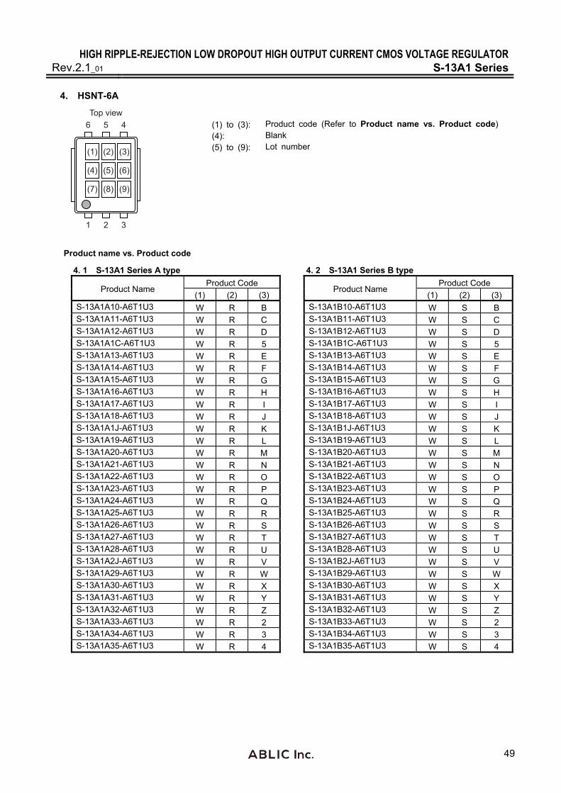
4. HSNT-6A
Top view
1 32
6 45
(1) (2) (3)
(4) (5) (6)
(7) (8) (9)
(1) to (3): Product code (Refer to Product name vs. Product code)
(4): Blank
(5) to (9): Lot number
Product name vs. Product code
4. 1 S-13A1 Series A type 4. 2 S-13A1 Series B type
Product Name Product Code
Product Name Product Code
(1) (2) (3) (1) (2) (3) S-13A1A10-A6T1U3 W R B S-13A1B10-A6T1U3 W S B S-13A1A11-A6T1U3 W R C S-13A1B11-A6T1U3 W S C S-13A1A12-A6T1U3 W R D S-13A1B12-A6T1U3 W S D S-13A1A1C-A6T1U3 W R 5 S-13A1B1C-A6T1U3 W S 5 S-13A1A13-A6T1U3 W R E S-13A1B13-A6T1U3 W S E S-13A1A14-A6T1U3 W R F S-13A1B14-A6T1U3 W S F S-13A1A15-A6T1U3 W R G S-13A1B15-A6T1U3 W S G S-13A1A16-A6T1U3 W R H S-13A1B16-A6T1U3 W S H S-13A1A17-A6T1U3 W R I S-13A1B17-A6T1U3 W S I S-13A1A18-A6T1U3 W R J S-13A1B18-A6T1U3 W S J S-13A1A1J-A6T1U3 W R K S-13A1B1J-A6T1U3 W S K S-13A1A19-A6T1U3 W R L S-13A1B19-A6T1U3 W S L S-13A1A20-A6T1U3 W R M S-13A1B20-A6T1U3 W S M S-13A1A21-A6T1U3 W R N S-13A1B21-A6T1U3 W S N S-13A1A22-A6T1U3 W R O S-13A1B22-A6T1U3 W S O S-13A1A23-A6T1U3 W R P S-13A1B23-A6T1U3 W S P S-13A1A24-A6T1U3 W R Q S-13A1B24-A6T1U3 W S Q S-13A1A25-A6T1U3 W R R S-13A1B25-A6T1U3 W S R S-13A1A26-A6T1U3 W R S S-13A1B26-A6T1U3 W S S S-13A1A27-A6T1U3 W R T S-13A1B27-A6T1U3 W S T S-13A1A28-A6T1U3 W R U S-13A1B28-A6T1U3 W S U S-13A1A2J-A6T1U3 W R V S-13A1B2J-A6T1U3 W S V S-13A1A29-A6T1U3 W R W S-13A1B29-A6T1U3 W S W S-13A1A30-A6T1U3 W R X S-13A1B30-A6T1U3 W S X S-13A1A31-A6T1U3 W R Y S-13A1B31-A6T1U3 W S Y S-13A1A32-A6T1U3 W R Z S-13A1B32-A6T1U3 W S Z S-13A1A33-A6T1U3 W R 2 S-13A1B33-A6T1U3 W S 2 S-13A1A34-A6T1U3 W R 3 S-13A1B34-A6T1U3 W S 3 S-13A1A35-A6T1U3 W R 4 S-13A1B35-A6T1U3 W S 4
HIGH RIPPLE-REJECTION LOW DROPOUT HIGH OUTPUT CURRENT CMOS VOLTAGE REGULATOR S-13A1 Series Rev.2.1_01
50
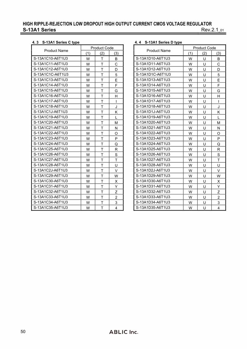
4. 3 S-13A1 Series C type 4. 4 S-13A1 Series D type
Product Name Product Code
Product Name Product Code
(1) (2) (3) (1) (2) (3) S-13A1C10-A6T1U3 W T B S-13A1D10-A6T1U3 W U B S-13A1C11-A6T1U3 W T C S-13A1D11-A6T1U3 W U C S-13A1C12-A6T1U3 W T D S-13A1D12-A6T1U3 W U D S-13A1C1C-A6T1U3 W T 5 S-13A1D1C-A6T1U3 W U 5 S-13A1C13-A6T1U3 W T E S-13A1D13-A6T1U3 W U E S-13A1C14-A6T1U3 W T F S-13A1D14-A6T1U3 W U F S-13A1C15-A6T1U3 W T G S-13A1D15-A6T1U3 W U G S-13A1C16-A6T1U3 W T H S-13A1D16-A6T1U3 W U H S-13A1C17-A6T1U3 W T I S-13A1D17-A6T1U3 W U I S-13A1C18-A6T1U3 W T J S-13A1D18-A6T1U3 W U J S-13A1C1J-A6T1U3 W T K S-13A1D1J-A6T1U3 W U K S-13A1C19-A6T1U3 W T L S-13A1D19-A6T1U3 W U L S-13A1C20-A6T1U3 W T M S-13A1D20-A6T1U3 W U M S-13A1C21-A6T1U3 W T N S-13A1D21-A6T1U3 W U N S-13A1C22-A6T1U3 W T O S-13A1D22-A6T1U3 W U O S-13A1C23-A6T1U3 W T P S-13A1D23-A6T1U3 W U P S-13A1C24-A6T1U3 W T Q S-13A1D24-A6T1U3 W U Q S-13A1C25-A6T1U3 W T R S-13A1D25-A6T1U3 W U R S-13A1C26-A6T1U3 W T S S-13A1D26-A6T1U3 W U S S-13A1C27-A6T1U3 W T T S-13A1D27-A6T1U3 W U T S-13A1C28-A6T1U3 W T U S-13A1D28-A6T1U3 W U U S-13A1C2J-A6T1U3 W T V S-13A1D2J-A6T1U3 W U V S-13A1C29-A6T1U3 W T W S-13A1D29-A6T1U3 W U W S-13A1C30-A6T1U3 W T X S-13A1D30-A6T1U3 W U X S-13A1C31-A6T1U3 W T Y S-13A1D31-A6T1U3 W U Y S-13A1C32-A6T1U3 W T Z S-13A1D32-A6T1U3 W U Z S-13A1C33-A6T1U3 W T 2 S-13A1D33-A6T1U3 W U 2 S-13A1C34-A6T1U3 W T 3 S-13A1D34-A6T1U3 W U 3 S-13A1C35-A6T1U3 W T 4 S-13A1D35-A6T1U3 W U 4
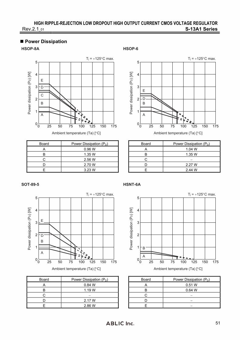
HIGH RIPPLE-REJECTION LOW DROPOUT HIGH OUTPUT CURRENT CMOS VOLTAGE REGULATORRev.2.1_01 S-13A1 Series
51
Power Dissipation
0 25 50 75 100 125 150 1750
1
2
3
4
5
Ambient temperature (Ta) [C]
Pow
er d
issi
patio
n (P
D) [
W]
Tj = 125C max.
HSOP-8A
E
D
C
B
A
0 25 50 75 100 125 150 1750
1
2
3
4
5
Ambient temperature (Ta) [C]P
ower
dis
sipa
tion
(PD) [
W]
Tj = 125C max.
HSOP-6
E
DB
A
Board Power Dissipation (PD) Board Power Dissipation (PD)
A 0.96 W A 1.04 W
B 1.35 W B 1.35 W
C 2.56 W C D 2.70 W D 2.27 W
E 3.23 W E 2.44 W
0 25 50 75 100 125 150 1750
1
2
3
4
5
Ambient temperature (Ta) [C]
Pow
er d
issi
patio
n (P
D) [
W]
Tj = 125C max.
SOT-89-5
E
DB
A
0 25 50 75 100 125 150 1750
1
2
3
4
5
Ambient temperature (Ta) [C]
Pow
er d
issi
patio
n (P
D) [
W]
Tj = 125C max.
HSNT-6A
B
A
Board Power Dissipation (PD) Board Power Dissipation (PD)
A 0.84 W A 0.51 W
B 1.19 W B 0.64 W
C C D 2.17 W D E 2.86 W E
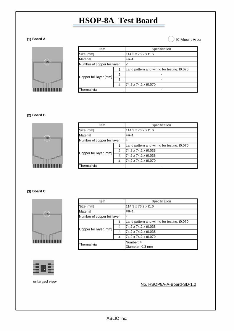
(1)
1234
(2)
1234
(3)
1234
Board A
Board B
Board C
Thermal via Number: 4Diameter: 0.3 mm
Number of copper foil layer 4
Copper foil layer [mm]
Land pattern and wiring for testing: t0.07074.2 x 74.2 x t0.03574.2 x 74.2 x t0.03574.2 x 74.2 x t0.070
Material FR-4
Thermal via -
Item Specification
Copper foil layer [mm]
Land pattern and wiring for testing: t0.07074.2 x 74.2 x t0.03574.2 x 74.2 x t0.03574.2 x 74.2 x t0.070
Size [mm] 114.3 x 76.2 x t1.6
Size [mm] 114.3 x 76.2 x t1.6Material FR-4Number of copper foil layer 4
Copper foil layer [mm]
Land pattern and wiring for testing: t0.070--
Item Specification
74.2 x 74.2 x t0.070
Size [mm] 114.3 x 76.2 x t1.6Item Specification
Thermal via -
Material FR-4Number of copper foil layer 2
IC Mount Area
enlarged view
HSOP-8A Test Board
No. HSOP8A-A-Board-SD-1.0
ABLIC Inc.
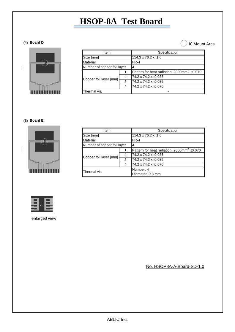
(4)
1234
(5)
1234
Size [mm] 114.3 x 76.2 x t1.6Material FR-4
Item Specification
Number of copper foil layer 4
Copper foil layer [mm]
Pattern for heat radiation: 2000mm2 t0.07074.2 x 74.2 x t0.03574.2 x 74.2 x t0.03574.2 x 74.2 x t0.070
74.2 x 74.2 x t0.070
Size [mm] 114.3 x 76.2 x t1.6Material FR-4
Thermal via -
Item Specification
Board D
Board E
Thermal via Number: 4Diameter: 0.3 mm
Number of copper foil layer 4
Copper foil layer [mm]
Pattern for heat radiation: 2000mm2 t0.07074.2 x 74.2 x t0.03574.2 x 74.2 x t0.035
enlarged view
IC Mount Area
HSOP-8A Test Board
No. HSOP8A-A-Board-SD-1.0
ABLIC Inc.
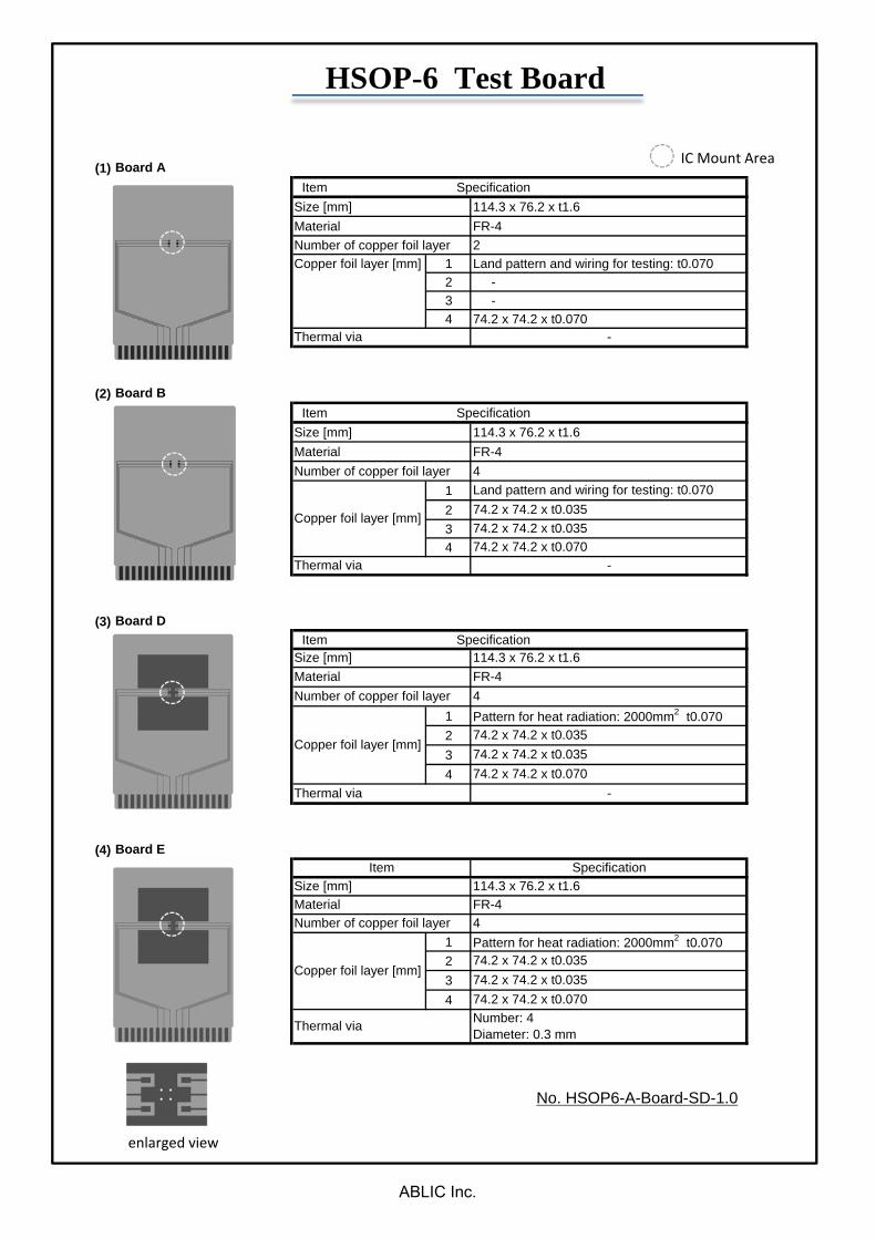
(1)Item Specification
Size [mm] 114.3 x 76.2 x t1.6Material FR-4Number of copper foil layer 2Copper foil layer [mm] 1 Land pattern and wiring for testing: t0.070
2 -3 -4 74.2 x 74.2 x t0.070
(2)Item Specification
Size [mm] 114.3 x 76.2 x t1.6Material FR-4Number of copper foil layer 4
1234
(3)Item Specification
1234
(4)
1234
Thermal via -
Material FR-4Number of copper foil layer 4
Board D
-Thermal via
74.2 x 74.2 x t0.035
Land pattern and wiring for testing: t0.070
114.3 x 76.2 x t1.6
Copper foil layer [mm]
Pattern for heat radiation: 2000mm2 t0.070
Thermal via Number: 4Diameter: 0.3 mm
Material FR-4Number of copper foil layer
Board A
74.2 x 74.2 x t0.070
Board B
74.2 x 74.2 x t0.03574.2 x 74.2 x t0.035
74.2 x 74.2 x t0.070
Board E
Thermal via -
Size [mm]
SpecificationItem
74.2 x 74.2 x t0.035Copper foil layer [mm]
4
Copper foil layer [mm]
Pattern for heat radiation: 2000mm2 t0.07074.2 x 74.2 x t0.035
74.2 x 74.2 x t0.070
Size [mm]
74.2 x 74.2 x t0.035
114.3 x 76.2 x t1.6
IC Mount Area
enlarged view
HSOP-6 Test Board
No. HSOP6-A-Board-SD-1.0
ABLIC Inc.
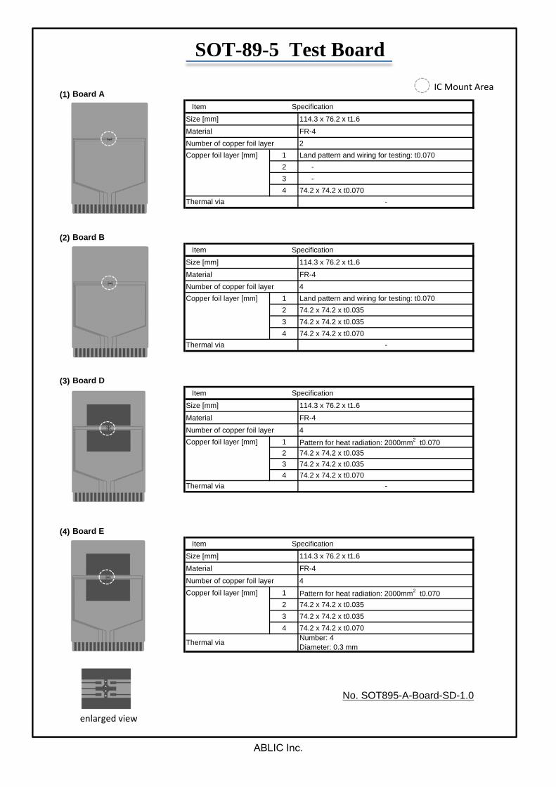
(1)Item Specification
Size [mm] 114.3 x 76.2 x t1.6
Material FR-4Number of copper foil layer 2Copper foil layer [mm] 1 Land pattern and wiring for testing: t0.070
2 -3 -4 74.2 x 74.2 x t0.070
(2)Item Specification
Size [mm] 114.3 x 76.2 x t1.6
Material FR-4Number of copper foil layer 4Copper foil layer [mm] 1 Land pattern and wiring for testing: t0.070
2 74.2 x 74.2 x t0.0353 74.2 x 74.2 x t0.0354 74.2 x 74.2 x t0.070
(3)Item Specification
Size [mm] 114.3 x 76.2 x t1.6
Material FR-4
Number of copper foil layer 4Copper foil layer [mm] 1 Pattern for heat radiation: 2000mm2 t0.070
2 74.2 x 74.2 x t0.0353 74.2 x 74.2 x t0.0354 74.2 x 74.2 x t0.070
(4)Item Specification
Size [mm] 114.3 x 76.2 x t1.6
Material FR-4
Number of copper foil layer 4Copper foil layer [mm] 1 Pattern for heat radiation: 2000mm2 t0.070
2 74.2 x 74.2 x t0.0353 74.2 x 74.2 x t0.0354 74.2 x 74.2 x t0.070
Board E
Thermal via Number: 4Diameter: 0.3 mm
Board D
Thermal via -
Board B
Thermal via -
Thermal via -
Board AIC Mount Area
enlarged view
SOT-89-5 Test Board
No. SOT895-A-Board-SD-1.0
ABLIC Inc.
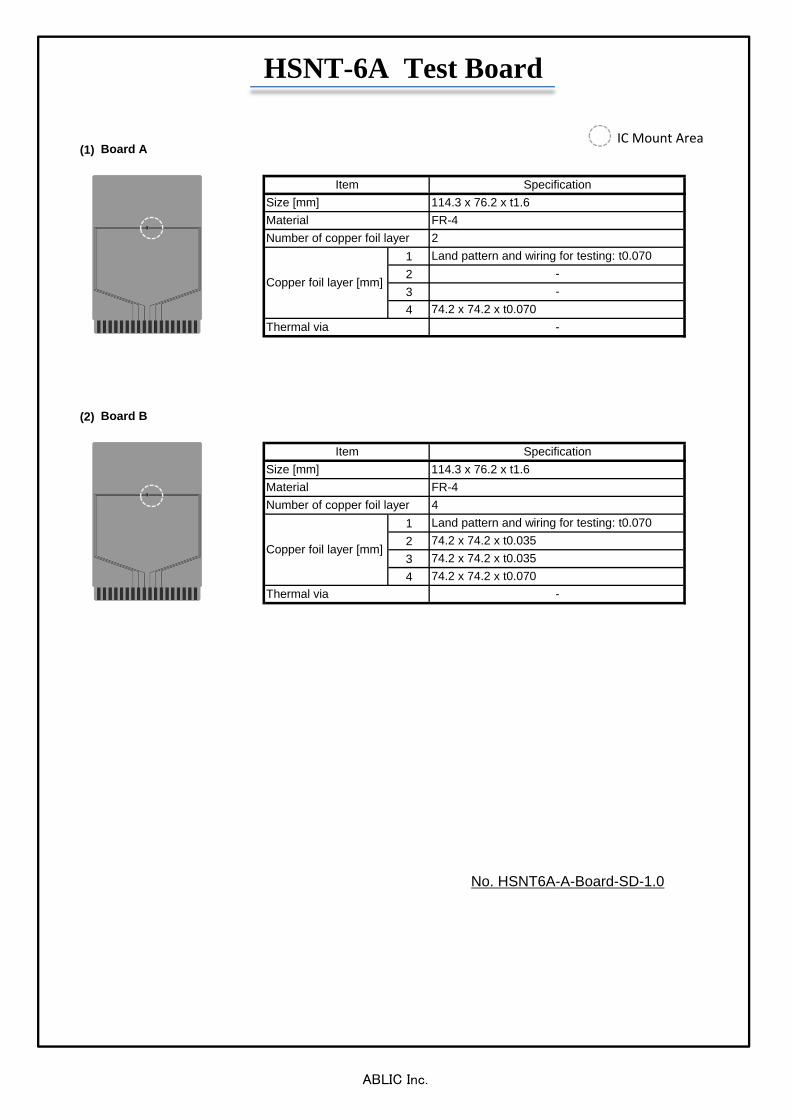
(1)
1234
(2)
1234
Thermal via -
Material FR-4Number of copper foil layer 4
Copper foil layer [mm]
Land pattern and wiring for testing: t0.07074.2 x 74.2 x t0.03574.2 x 74.2 x t0.03574.2 x 74.2 x t0.070
Thermal via -
Board B
Item SpecificationSize [mm] 114.3 x 76.2 x t1.6
Number of copper foil layer 2
Copper foil layer [mm]
Land pattern and wiring for testing: t0.070--
74.2 x 74.2 x t0.070
Board A
Item SpecificationSize [mm] 114.3 x 76.2 x t1.6Material FR-4
IC Mount Area
HSNT-6A Test Board
No. HSNT6A-A-Board-SD-1.0
ABLIC Inc.
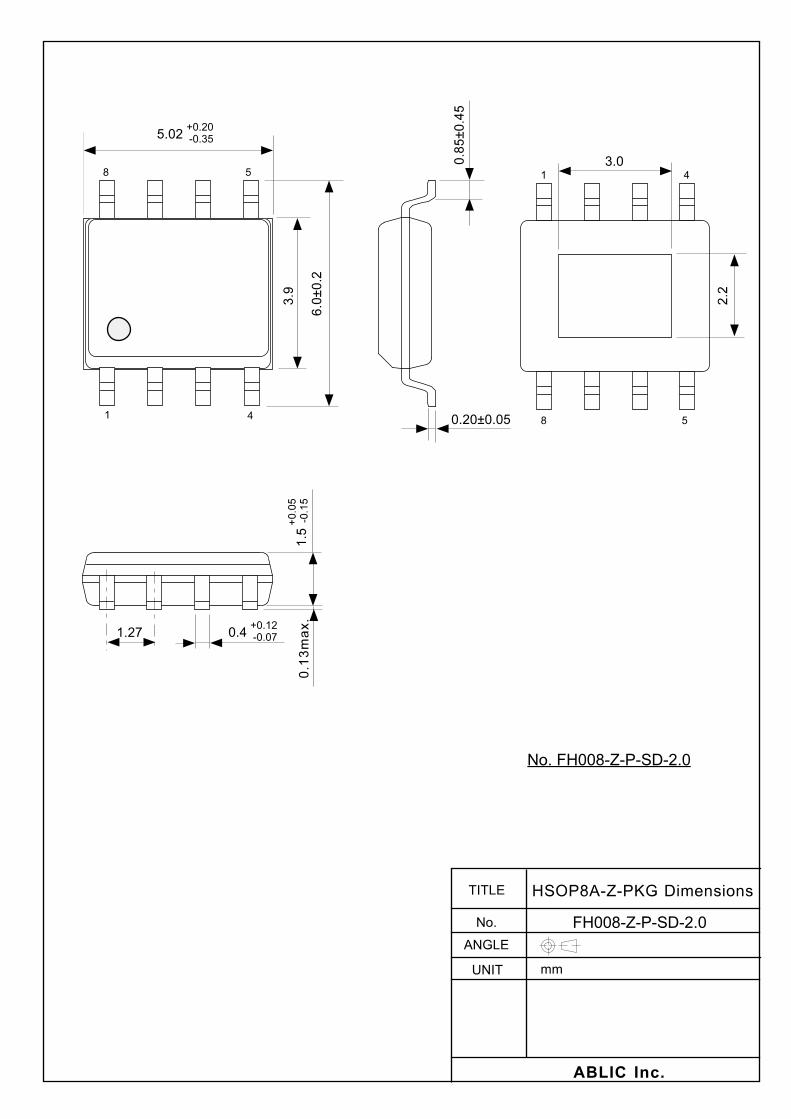
������ ��
���
�����
���
����
���� ���������������
��
����������������������
���������������
������������ �
��!���"�����#"��#
����$����" !
� � " !
� �
��
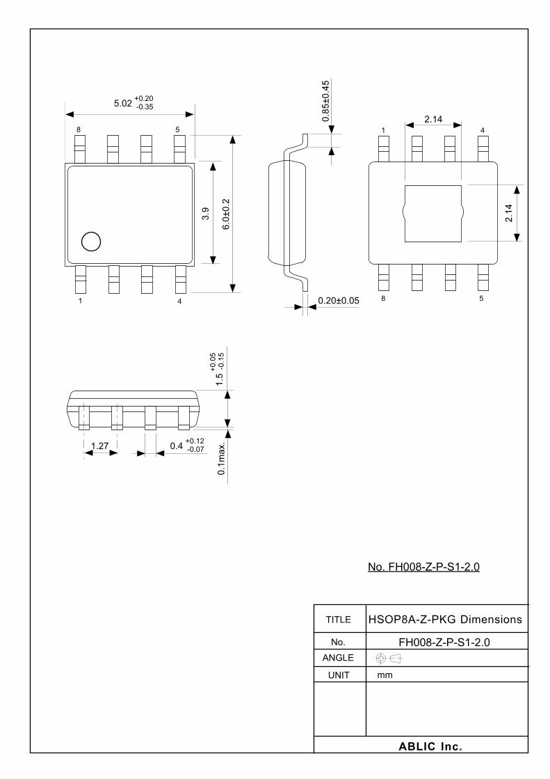
������ ��
���
�����
���
����
���� ����������"����
��
����������������������
����������"����
"��#
����$����" !
� �
������������ �
��!���"�����#
" !
� �
��"!
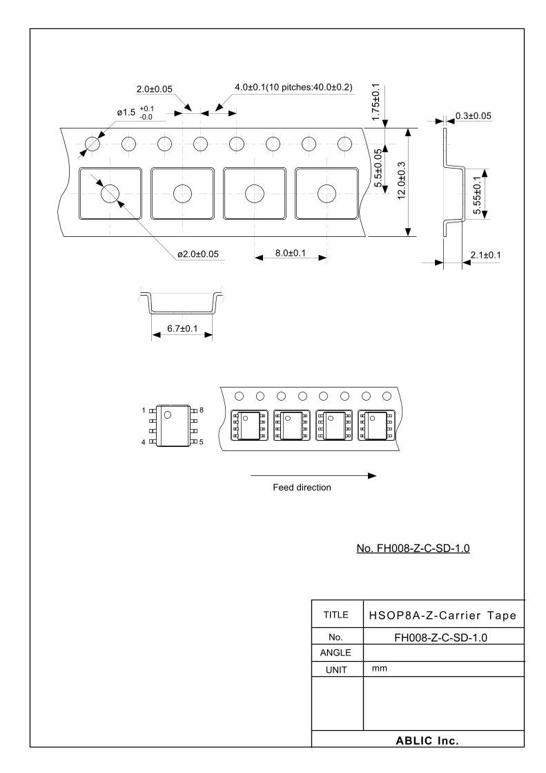
������ ��
���
�����
���
����
��
%���$����
%"�� �� $����
��"$��"���$��"
&�#$��"
���$���� !��$��"'"��(�)*+��,!���$���-
��������./00 ��0 � �/(�
�������.����"��
���"����
���� �������.����"��
�
�"
!
��1�1�0�*)���

������ ��
���
�����
���
����
��
�
�"
!
%"�� ����$�����
��"$��"���$��"
&�!$��"
���$����
��1�1�0�*)���
!��$��"'"��(�)*+��,!���$���-
��������./00 ��0 � �/(�
���� �������.��"�"��
�������.��"�"��
���"��
%"���������
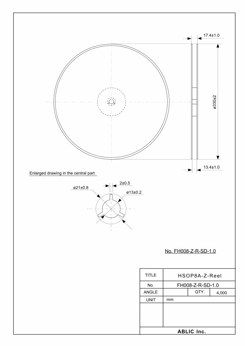
������ ��
���
�����
���
����
��
2�3� !4���
��������5��6
���� �������5����"��
�������5����"��
�$���
%" $���%�"$���
��6/07�1�10/8��7����)+��*��)0/6�(/0)
"#�!$"��
" �!$"��
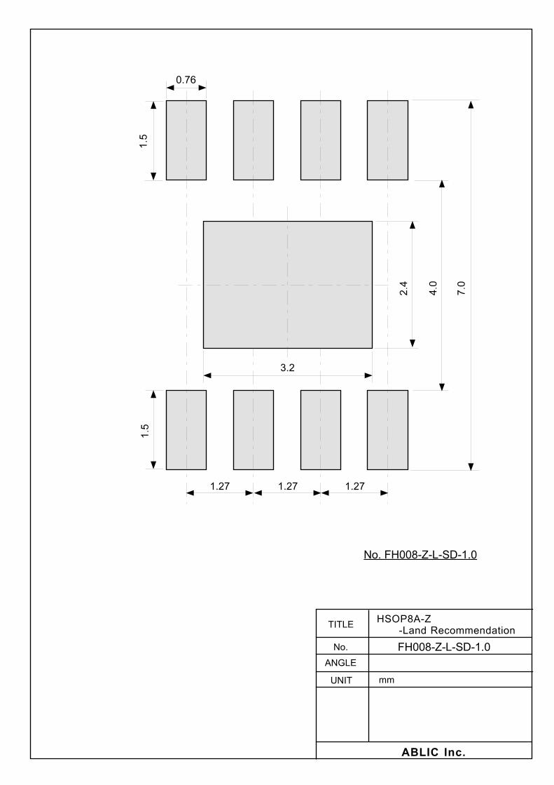
������ ��
���
�����
���
����
��
���������������/�1�5�*�����1/)���
������������"��
"��#
��#&
"��# "��#
��
���� ������������"��
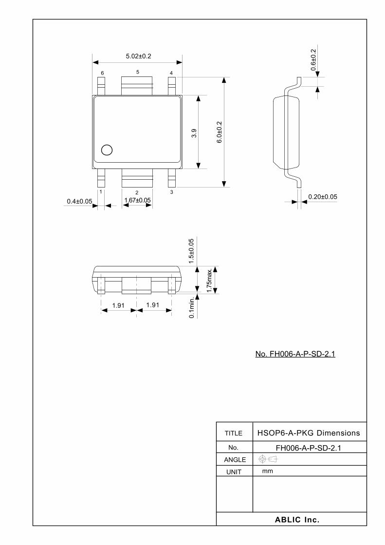
���
�����
���
����
������ ��
���� ��������������
��
��������������������
��������������
�������
��!�
�������
� "
� �
��!�
���#����
���������
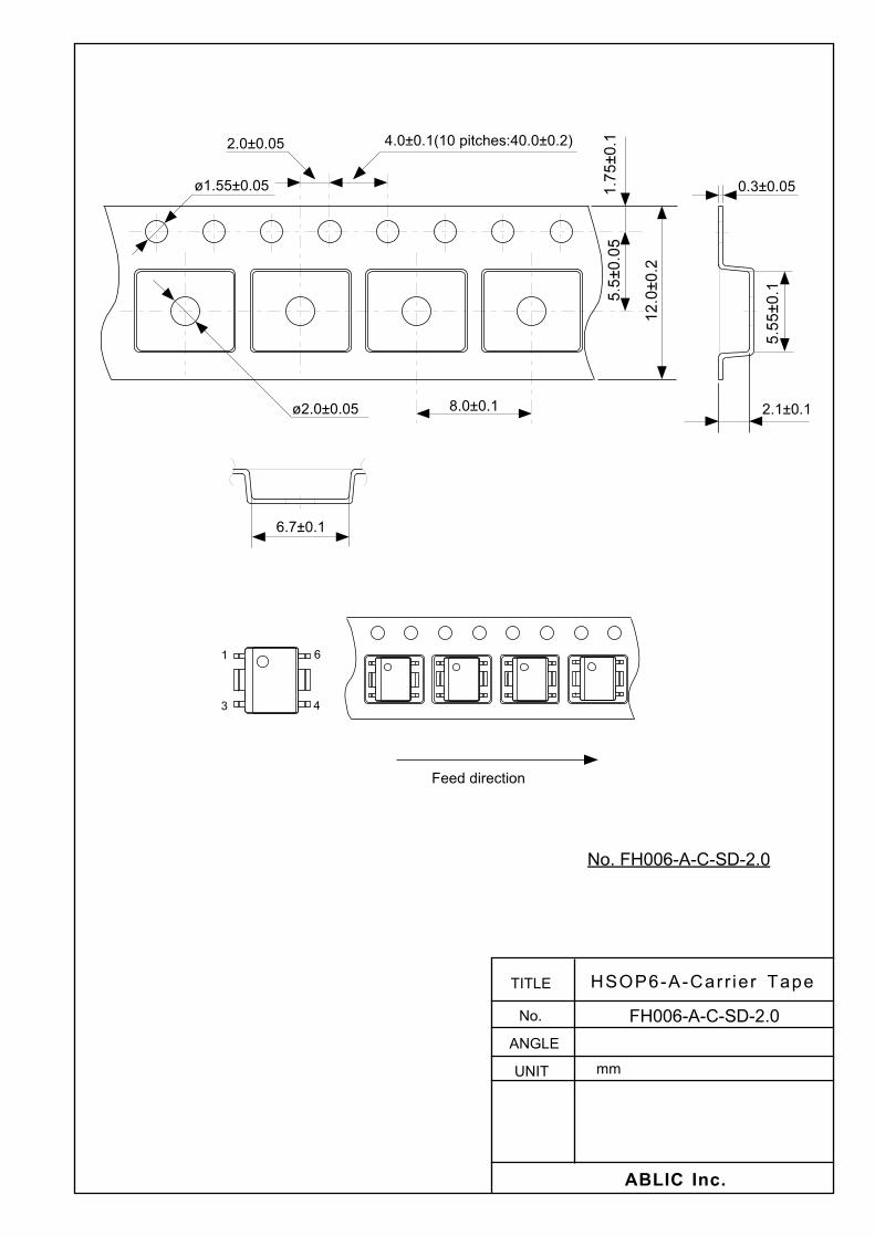
���
�����
���
����
������ ��
��
�
��
"
$�������
$�� ���� ��"����
�������%������
��#����
�������
��&�&�'�()���
�������*���+�)(,��-��������.
�������/0'' ��' � �0+�
������/�������
���� ������/�������
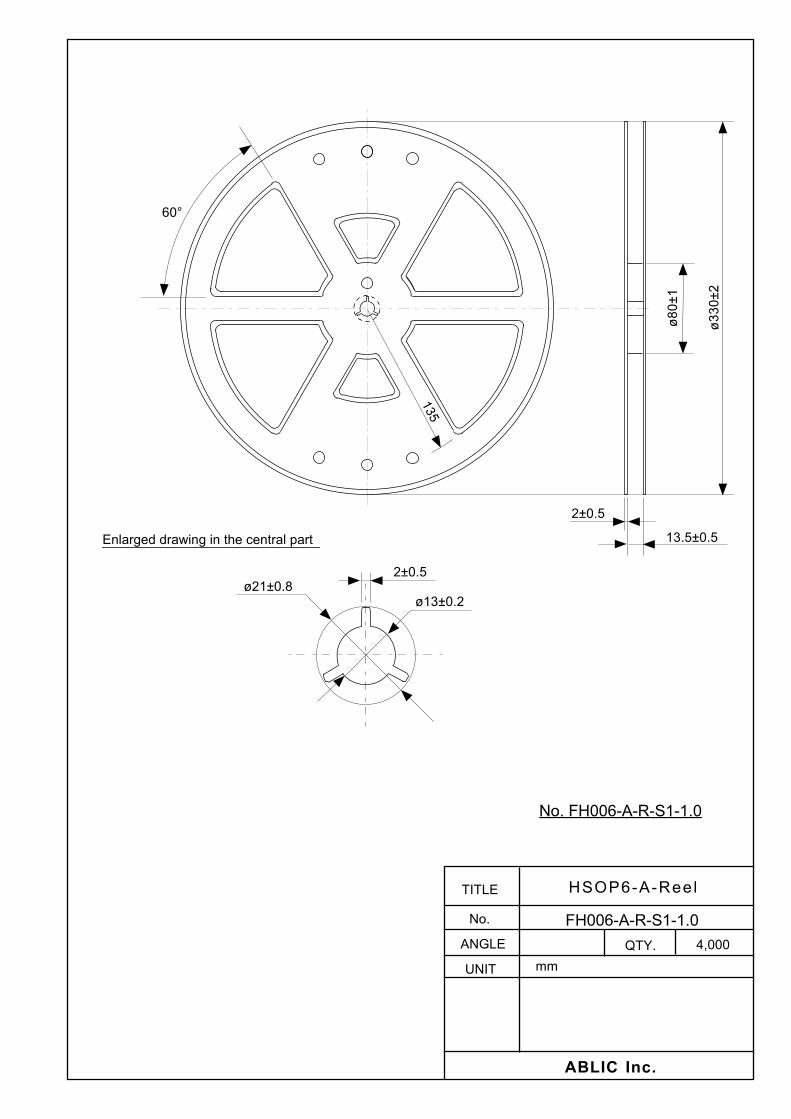
���
�����
���
����
������ ��
��
1�2� �3���
����
�"� ���
��4
����
$�"����$�����%
��50'6�&�&'07��6����),��(��)'05�+0')
�������8��5
���� ������8�������
������8�������
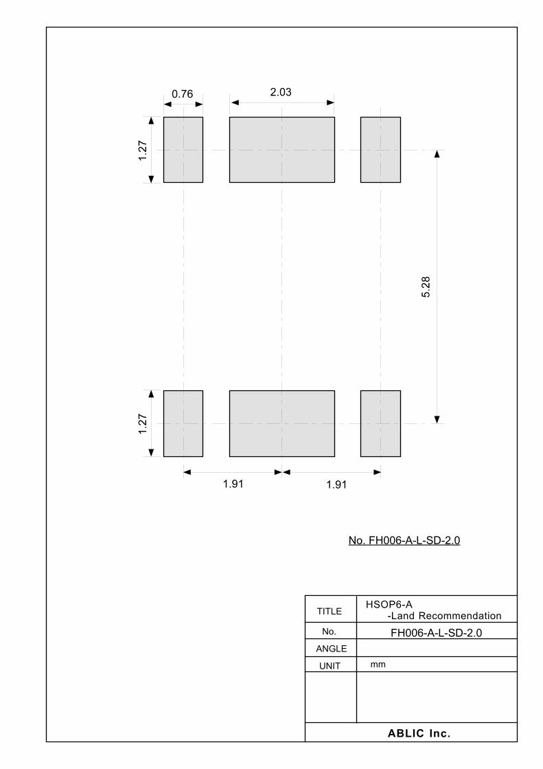
���
�����
���
����
������ ��
��
��������������0�&�8�(�����&0)���
���� ��������������
��������������
��#�
��!� ��!�
���"
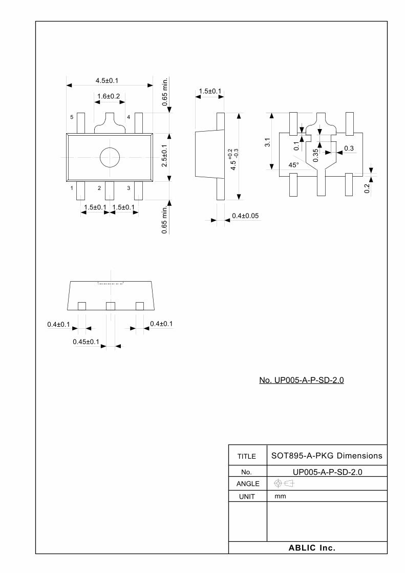
���
�����
���
����
������ ��
�� ���� �� ����
�������
�� ����
� ��
�� ����
�������
�������
��� ����
�������
�
����� ���������� !�� !
������� ����������
��� ����������
� "
���
��
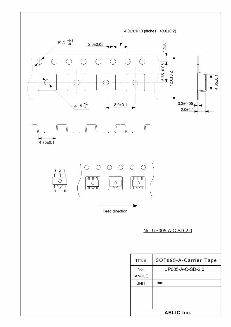
���
�����
���
����
������ ��
�������
������� �������#�� $������
������� #�� $���
���
��% ����
�� �
�
������� ��&�������
��� ��&�������
����� ��&'(( �� ( � �')�
*��+�+�(�,-��
�������.���)�-,/�!�0���������1
��
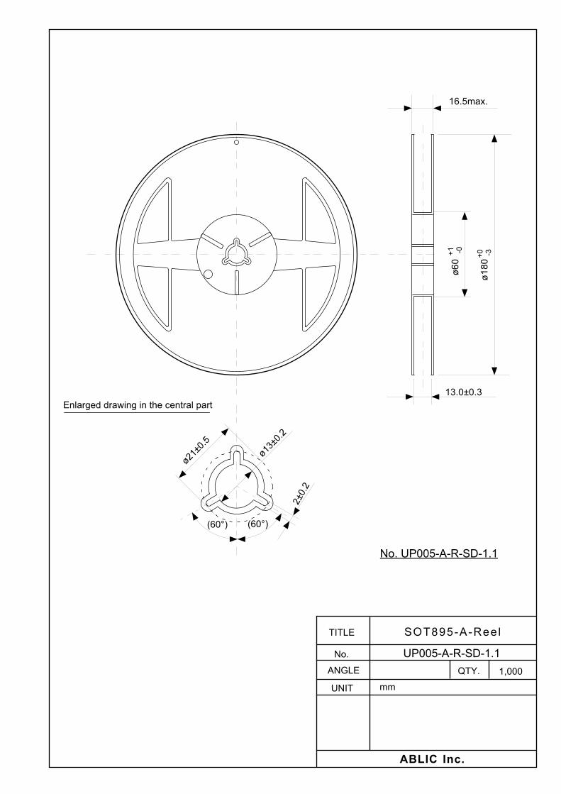
���
�����
���
����
������ ��
��� �'2�
��������
3�4� �5���
.��"1.��"1
������� ��6�������
��� ��6�������
����� ��6��7
� 7'(8�+�+('9� 8�� �-/��,� -('7�)'(-
��
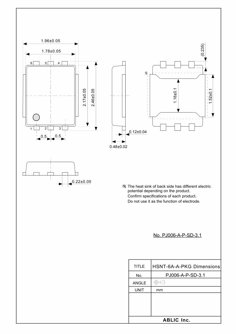
���
�����
���
����
������ ��
��
���������������������
���������������
�������������������
���������
�� !�����
��������
���
��"������
� � �
��
��� ���
��#!�����
�$��$�%&����'��(�)%*'���+��$%��+�((�,��&��-�*&,�*.�&��&�%-�+�.��+��/����&$��.,�+0*&�
1��(�,���.�*�(�*%&������(��%*$�.,�+0*&�
�����&�0����&�%��&$��(0�*&�����(��-�*&,�+��
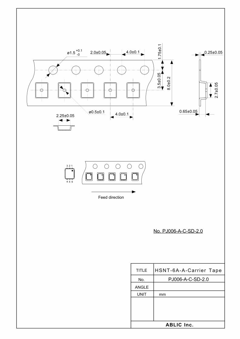
���
�����
���
����
������ ��
��
�������1�������
�������1%,, �� , � �%.�
2��+�+�,�*&���
��������������
������
3���4���
���
3����������������
���������
���������
� ��
��
���
�����������1�������
��� ������ ��� ���
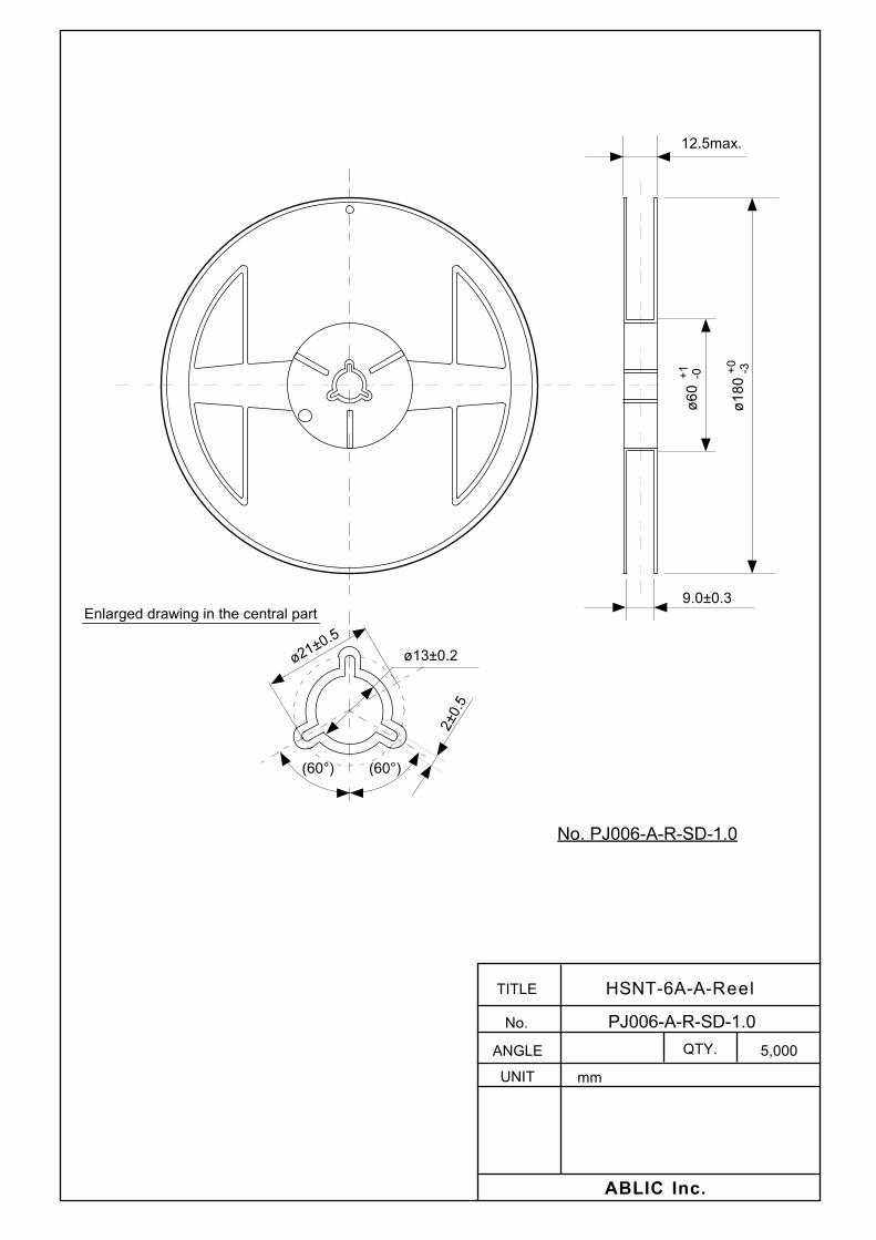
���
�����
���
����
������ ��
�����%5�
"������
3������
6��78 6��78
9�:� �;���
�����������<�������
�������<�������
��-%,/�+�+,%=��/����&$��*��&,%-�.%,&
��
�������<��-
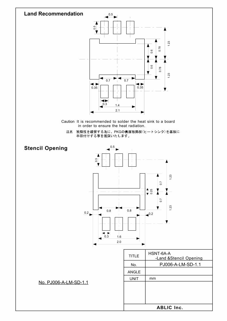
���
�����
���
����
������ ��
��
��������������%�+�B�&��*�-�C.����/
��������>�������
������������>�������
���
���
��
���
��# ��#
���� ����
����� ������������
���
���
���
���
��!��� ���
��!
���������������
1%0&������&� ��� ,�*�����+�+�&����-+�,� &$��$�%&����'�&��%�)�%,+��� � � � � � � � � � ����,+�,�&�����0,��&$��$�%&�,%+�%&����
���
Disclaimers (Handling Precautions)
1. All the information described herein (product data, specifications, figures, tables, programs, algorithms and application circuit examples, etc.) is current as of publishing date of this document and is subject to change without notice.
2. The circuit examples and the usages described herein are for reference only, and do not guarantee the success of any specific mass-production design. ABLIC Inc. is not responsible for damages caused by the reasons other than the products described herein (hereinafter "the products") or infringement of third-party intellectual property right and any other right due to the use of the information described herein.
3. ABLIC Inc. is not responsible for damages caused by the incorrect information described herein.
4. Be careful to use the products within their specified ranges. Pay special attention to the absolute maximum ratings, operation voltage range and electrical characteristics, etc. ABLIC Inc. is not responsible for damages caused by failures and / or accidents, etc. that occur due to the use of the products outside their specified ranges.
5. When using the products, confirm their applications, and the laws and regulations of the region or country where they are used and verify suitability, safety and other factors for the intended use.
6. When exporting the products, comply with the Foreign Exchange and Foreign Trade Act and all other export-related laws, and follow the required procedures.
7. The products must not be used or provided (exported) for the purposes of the development of weapons of mass destruction or military use. ABLIC Inc. is not responsible for any provision (export) to those whose purpose is to develop, manufacture, use or store nuclear, biological or chemical weapons, missiles, or other military use.
8. The products are not designed to be used as part of any device or equipment that may affect the human body, human life, or assets (such as medical equipment, disaster prevention systems, security systems, combustion control systems, infrastructure control systems, vehicle equipment, traffic systems, in-vehicle equipment, aviation equipment, aerospace equipment, and nuclear-related equipment), excluding when specified for in-vehicle use or other uses. Do not apply the products to the above listed devices and equipments without prior written permission by ABLIC Inc. Especially, the products cannot be used for life support devices, devices implanted in the human body and devices that directly affect human life, etc. Prior consultation with our sales office is required when considering the above uses. ABLIC Inc. is not responsible for damages caused by unauthorized or unspecified use of our products.
9. Semiconductor products may fail or malfunction with some probability. The user of the products should therefore take responsibility to give thorough consideration to safety design including redundancy, fire spread prevention measures, and malfunction prevention to prevent accidents causing injury or death, fires and social damage, etc. that may ensue from the products' failure or malfunction. The entire system must be sufficiently evaluated and applied on customer's own responsibility.
10. The products are not designed to be radiation-proof. The necessary radiation measures should be taken in the product design by the customer depending on the intended use.
11. The products do not affect human health under normal use. However, they contain chemical substances and heavy metals and should therefore not be put in the mouth. The fracture surfaces of wafers and chips may be sharp. Be careful when handling these with the bare hands to prevent injuries, etc.
12. When disposing of the products, comply with the laws and ordinances of the country or region where they are used.
13. The information described herein contains copyright information and know-how of ABLIC Inc. The information described herein does not convey any license under any intellectual property rights or any other rights belonging to ABLIC Inc. or a third party. Reproduction or copying of the information from this document or any part of this document described herein for the purpose of disclosing it to a third-party without the express permission of ABLIC Inc. is strictly prohibited.
14. For more details on the information described herein, contact our sales office.
2.2-2018.06
www.ablic.com