Embed Size (px)
Citation preview
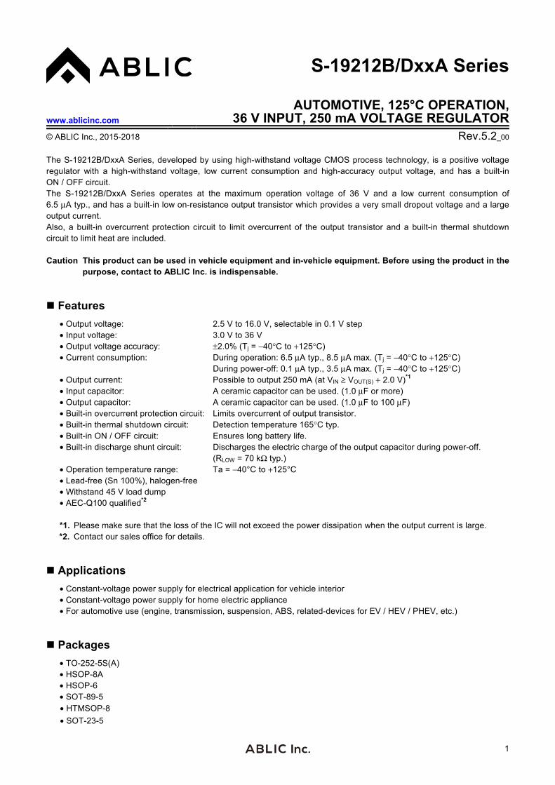
S-19212B/DxxA Series
AUTOMOTIVE, 125°C OPERATION,36 V INPUT, 250 mA VOLTAGE REGULATORwww.ablicinc.com
© ABLIC Inc., 2015-2018 Rev.5.2_00
1
The S-19212B/DxxA Series, developed by using high-withstand voltage CMOS process technology, is a positive voltage regulator with a high-withstand voltage, low current consumption and high-accuracy output voltage, and has a built-in ON / OFF circuit. The S-19212B/DxxA Series operates at the maximum operation voltage of 36 V and a low current consumption of 6.5 μA typ., and has a built-in low on-resistance output transistor which provides a very small dropout voltage and a large output current. Also, a built-in overcurrent protection circuit to limit overcurrent of the output transistor and a built-in thermal shutdown circuit to limit heat are included. Caution This product can be used in vehicle equipment and in-vehicle equipment. Before using the product in the
purpose, contact to ABLIC Inc. is indispensable.
Features
• Output voltage: 2.5 V to 16.0 V, selectable in 0.1 V step • Input voltage: 3.0 V to 36 V • Output voltage accuracy: ±2.0% (Tj = −40°C to +125°C) • Current consumption: During operation: 6.5 μA typ., 8.5 μA max. (Tj = −40°C to +125°C) During power-off: 0.1 μA typ., 3.5 μA max. (Tj = −40°C to +125°C) • Output current: Possible to output 250 mA (at VIN ≥ VOUT(S) + 2.0 V)*1 • Input capacitor: A ceramic capacitor can be used. (1.0 μF or more) • Output capacitor: A ceramic capacitor can be used. (1.0 μF to 100 μF) • Built-in overcurrent protection circuit: Limits overcurrent of output transistor. • Built-in thermal shutdown circuit: Detection temperature 165°C typ. • Built-in ON / OFF circuit: Ensures long battery life. • Built-in discharge shunt circuit: Discharges the electric charge of the output capacitor during power-off. (RLOW = 70 kΩ typ.) • Operation temperature range: Ta = −40°C to +125°C • Lead-free (Sn 100%), halogen-free • Withstand 45 V load dump • AEC-Q100 qualified*2 *1. Please make sure that the loss of the IC will not exceed the power dissipation when the output current is large. *2. Contact our sales office for details.
Applications
• Constant-voltage power supply for electrical application for vehicle interior • Constant-voltage power supply for home electric appliance • For automotive use (engine, transmission, suspension, ABS, related-devices for EV / HEV / PHEV, etc.)
Packages
• TO-252-5S(A) • HSOP-8A • HSOP-6 • SOT-89-5 • HTMSOP-8
• SOT-23-5
AUTOMOTIVE, 125°C OPERATION, 36 V INPUT, 250 mA VOLTAGE REGULATOR S-19212B/DxxA Series Rev.5.2_00
2
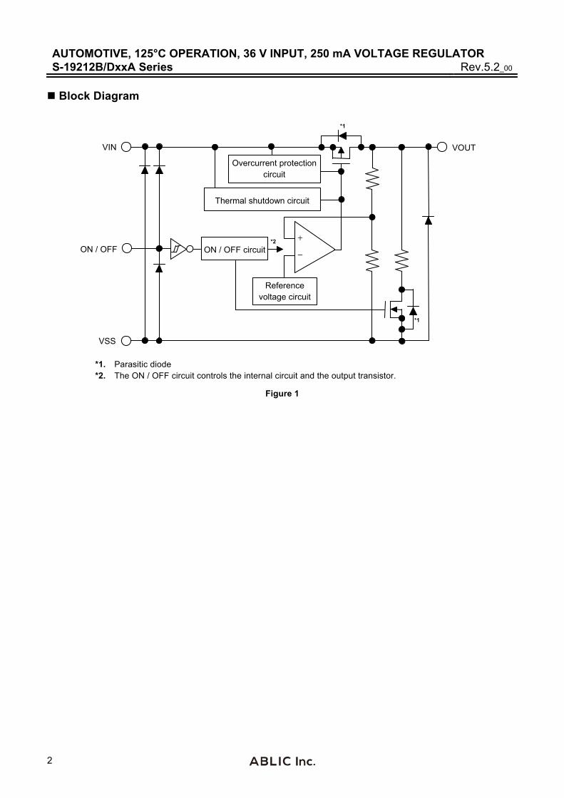
Block Diagram
Reference voltage circuit
ON / OFF
*1
ON / OFF circuit
+
−
VIN
VSS
VOUT
Overcurrent protection circuit
Thermal shutdown circuit
*1
*2
*1. Parasitic diode *2. The ON / OFF circuit controls the internal circuit and the output transistor.
Figure 1
AUTOMOTIVE, 125°C OPERATION, 36 V INPUT, 250 mA VOLTAGE REGULATORRev.5.2_00 S-19212B/DxxA Series
3
AEC-Q100 Qualified
This IC supports AEC-Q100 for operation temperature grade 1. Contact our sales office for details of AEC-Q100 reliability specification.
Product Name Structure
Users can select the output voltage and package type for the S-19212B/DxxA Series. Refer to "1. Product name" regarding the contents of product name, "2. Function list of product types" regarding the product type, "3. Packages" regarding the package drawings and "4. Product name list" for details of product names. 1. Product name
S-19212 x xx A - xxxx U
Package abbreviation and IC packing specifications*1 V5T2: TO-252-5S(A), Tape E8T1: HSOP-8A, Tape E6T1: HSOP-6, Tape U5T1: SOT-89-5, Tape S8T1: HTMSOP-8, Tape M5T1: SOT-23-5, Tape
Operation temperature A: Ta = −40°C to +125°C
Set output voltage 25 to G0 (e.g., when the set output voltage is 2.5 V, it is expressed as 25. when the set output voltage is 10.0 V, it is expressed as A0. when the set output voltage is 11.0 V, it is expressed as B0. when the set output voltage is 16.0 V, it is expressed as G0.)
Product type*2 B, D
Environmental code U: Lead-free (Sn 100%), halogen-free
*1. Refer to the tape drawing. *2. Refer to "2. Function list of product types" and "3. ON / OFF pin" in " Operation".
2. Function list of product types
Table 1
Product Type ON / OFF Logic ON / OFF pin input voltage "H" ON / OFF pin input voltage "L"
B Active "H" 1.5 V min. 0.25 V max.
D Active "H" 2.0 V min. 0.8 V max.
AUTOMOTIVE, 125°C OPERATION, 36 V INPUT, 250 mA VOLTAGE REGULATOR S-19212B/DxxA Series Rev.5.2_00
4
3. Packages
Table 2 Package Drawing Codes
Package Name Dimension Tape Reel Land
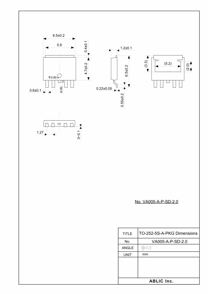
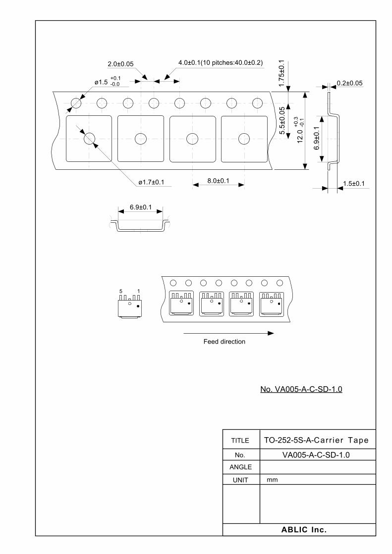
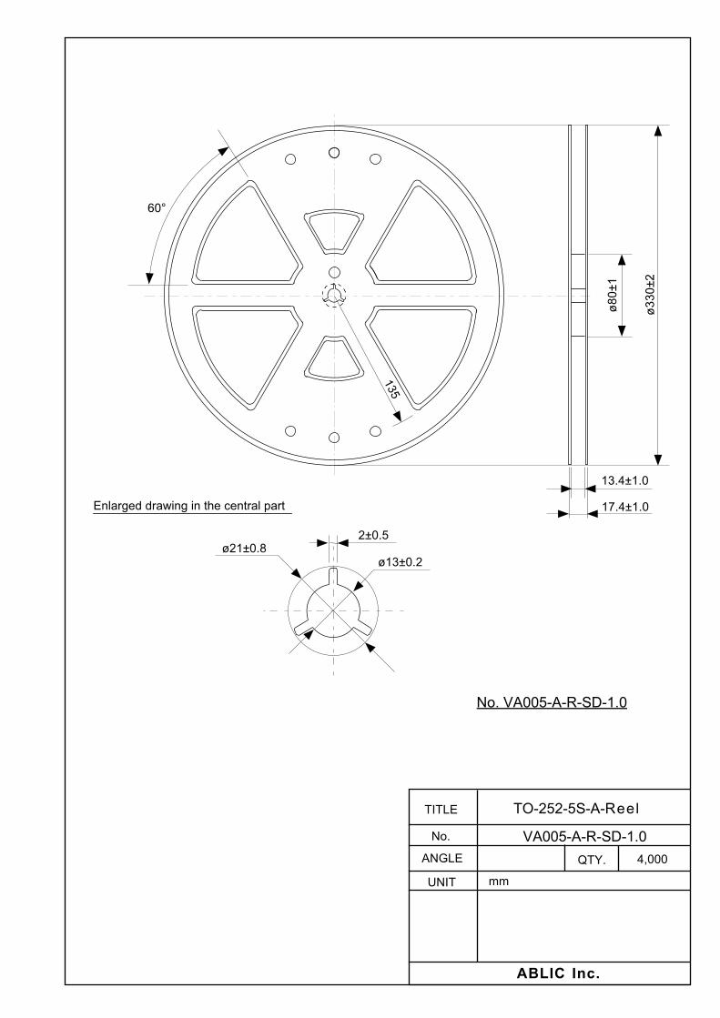
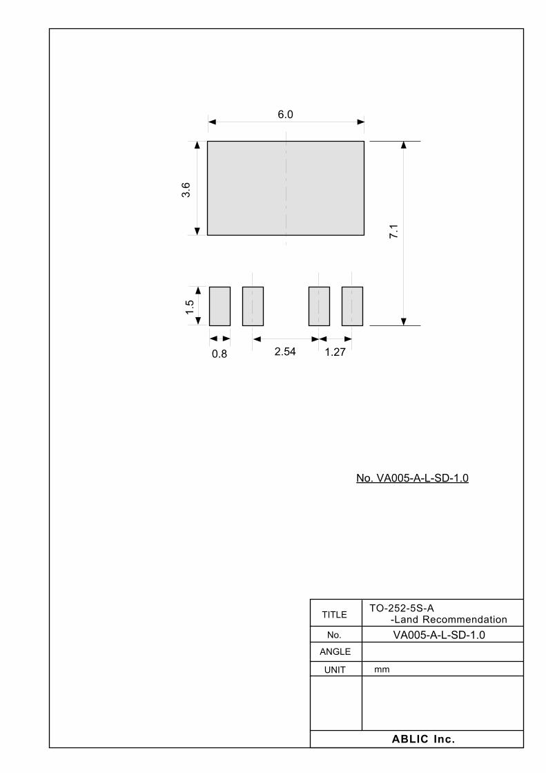
TO-252-5S(A) VA005-A-P-SD VA005-A-C-SD VA005-A-R-SD VA005-A-L-SD
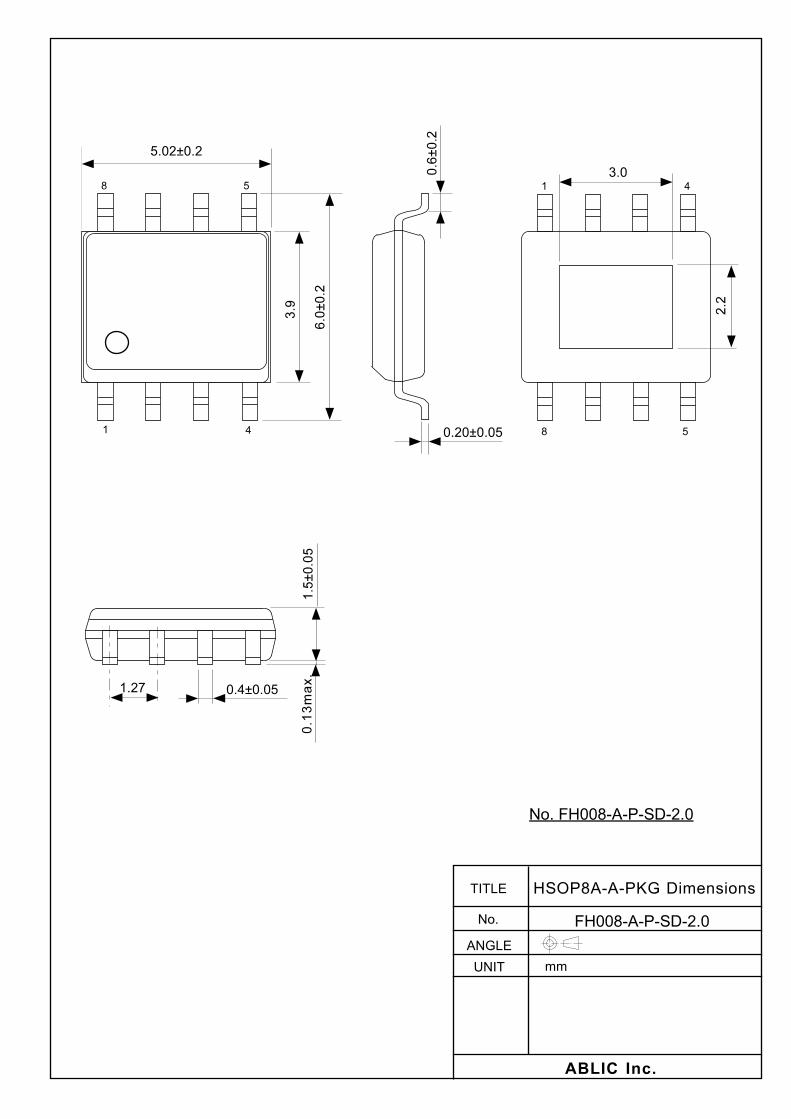
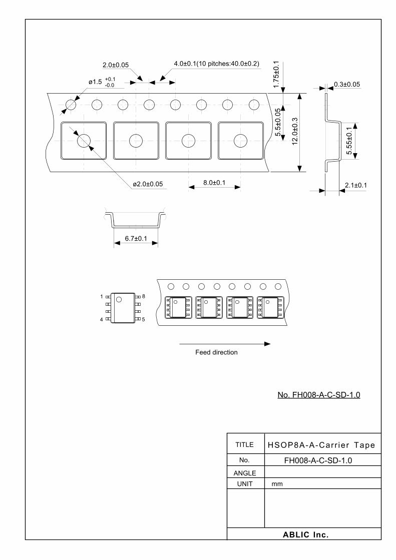
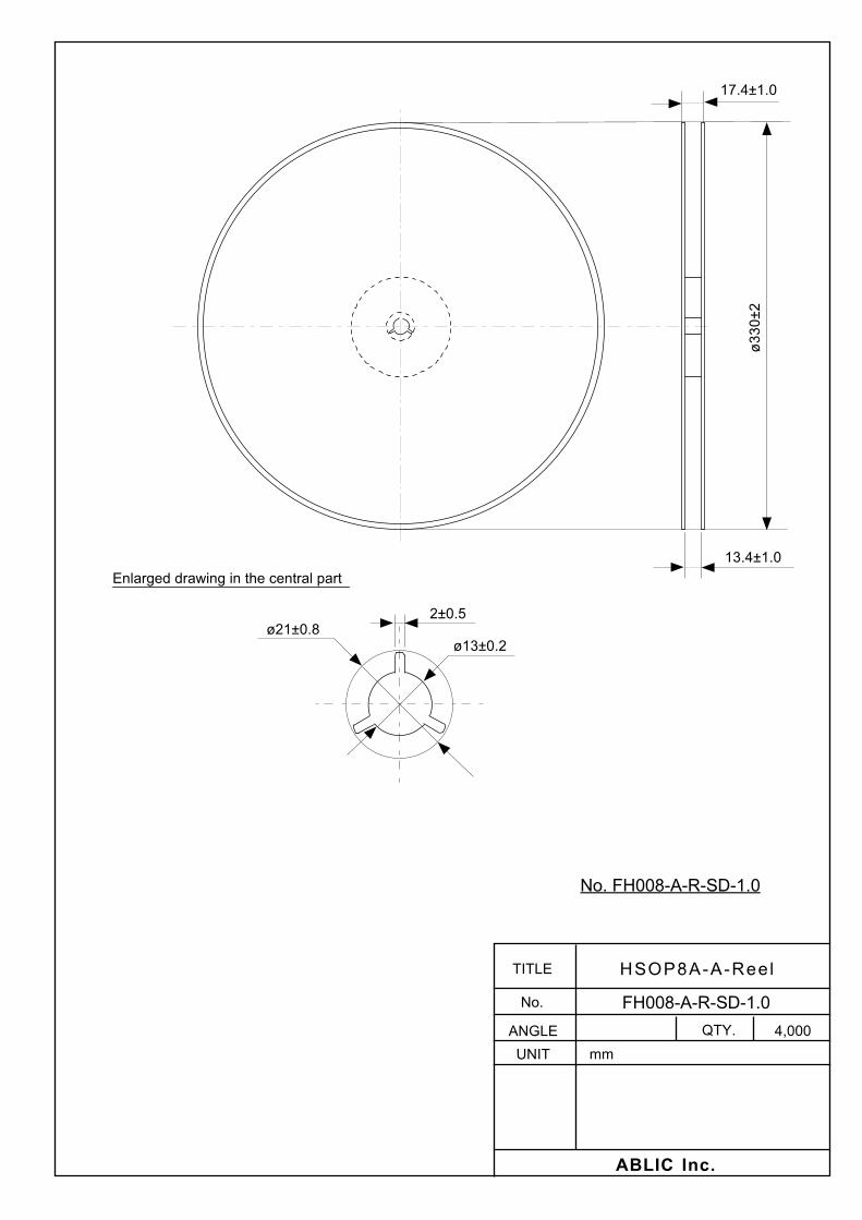
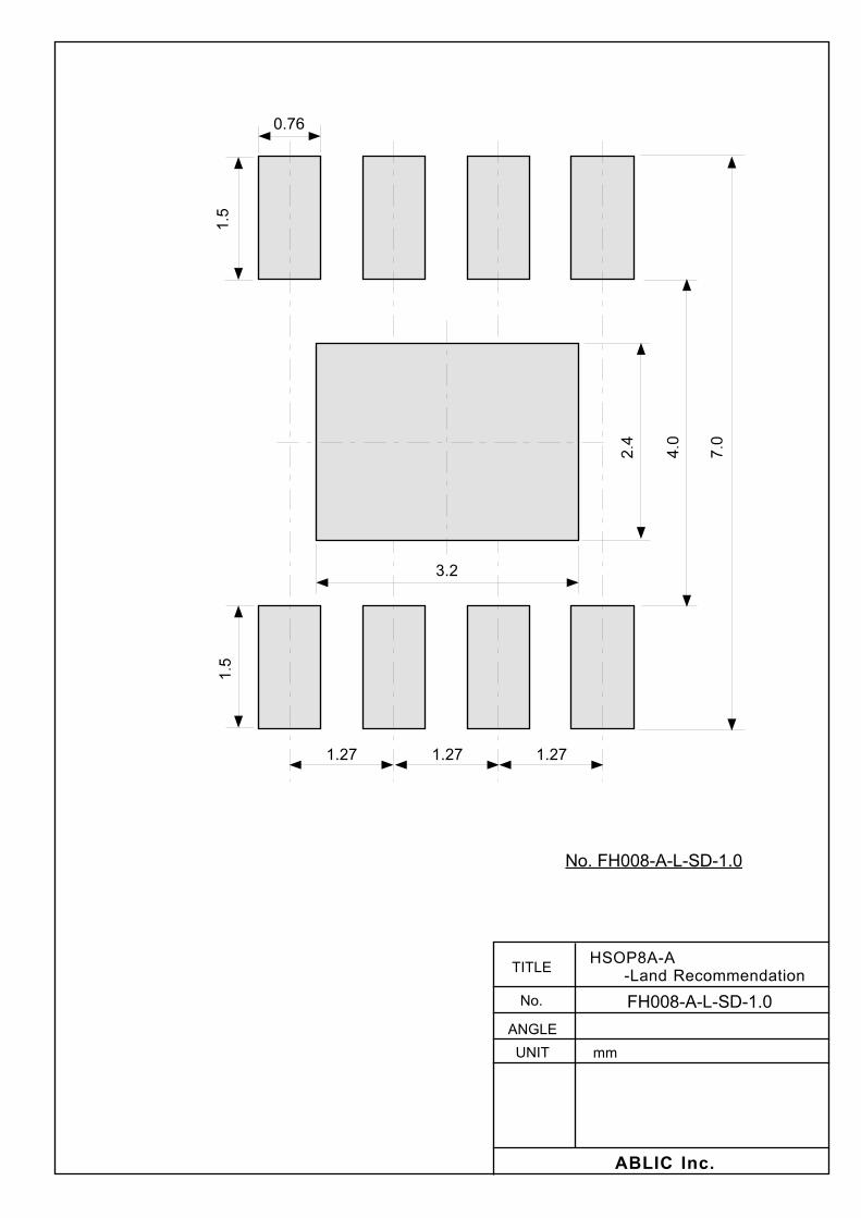
HSOP-8A FH008-A-P-SD FH008-A-C-SD FH008-A-R-SD FH008-A-L-SD
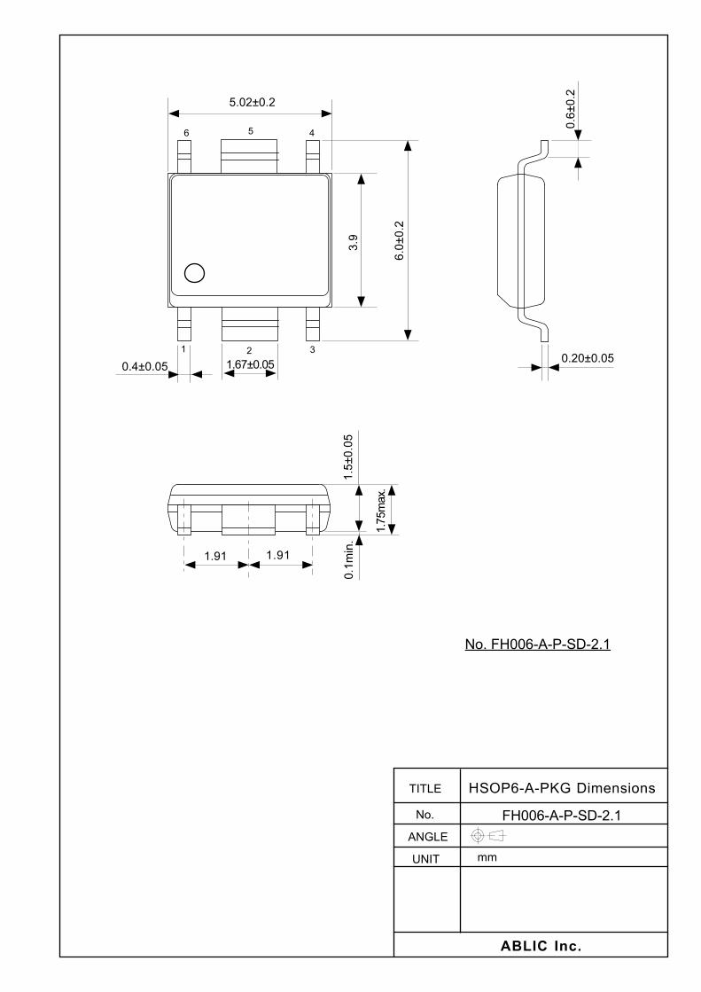
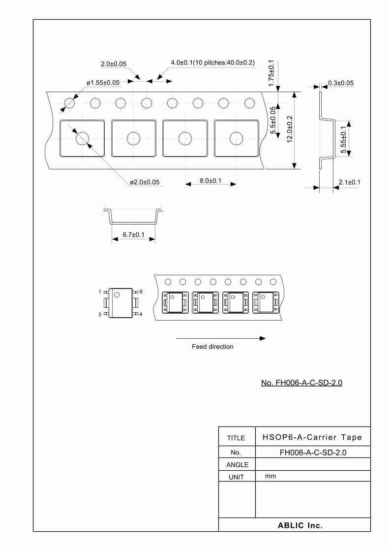
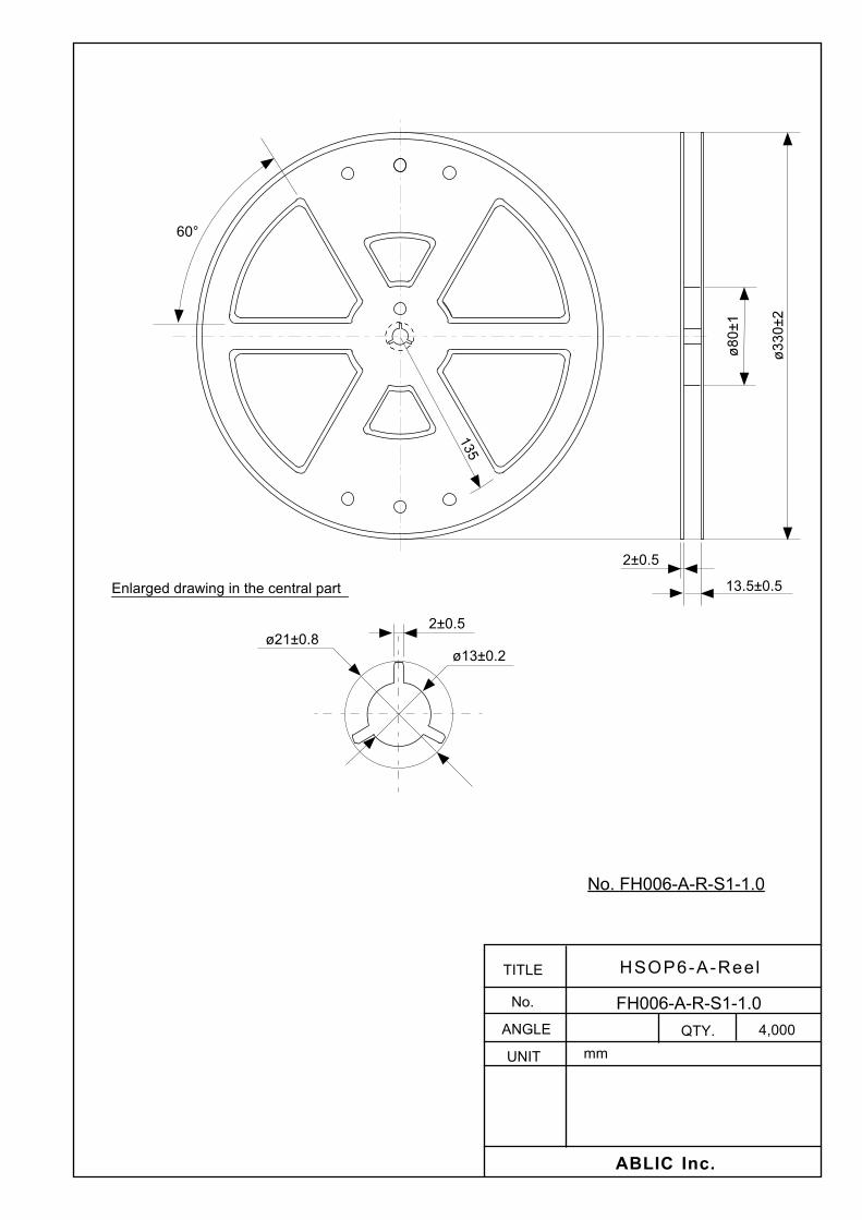
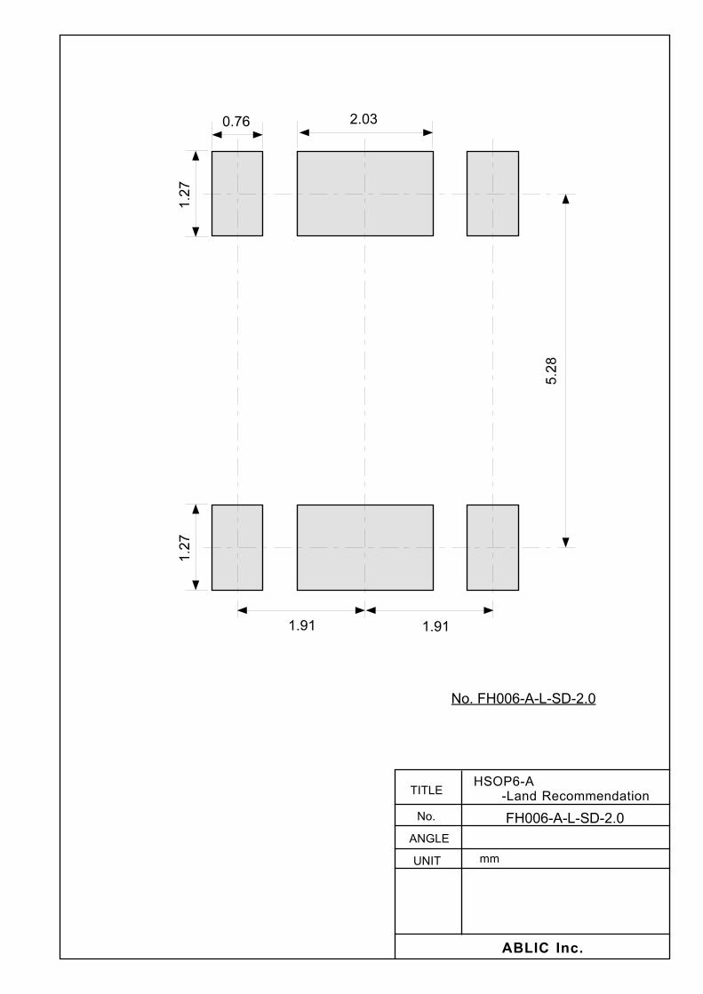
HSOP-6 FH006-A-P-SD FH006-A-C-SD FH006-A-R-S1 FH006-A-L-SD
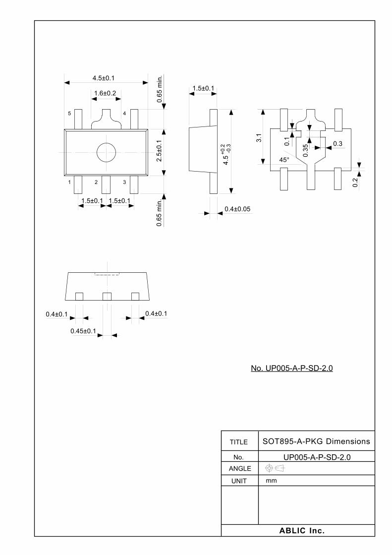
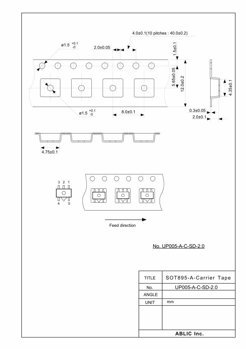
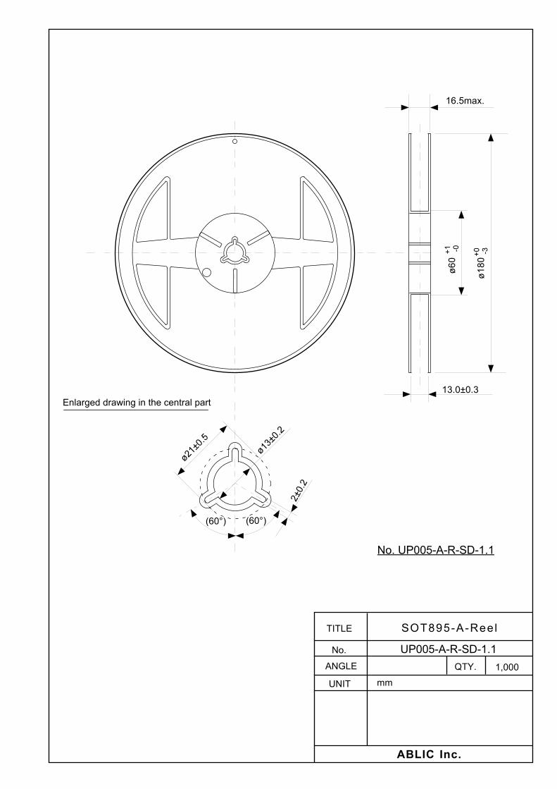
SOT-89-5 UP005-A-P-SD UP005-A-C-SD UP005-A-R-SD −
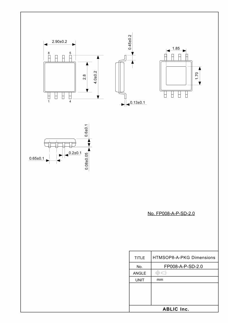
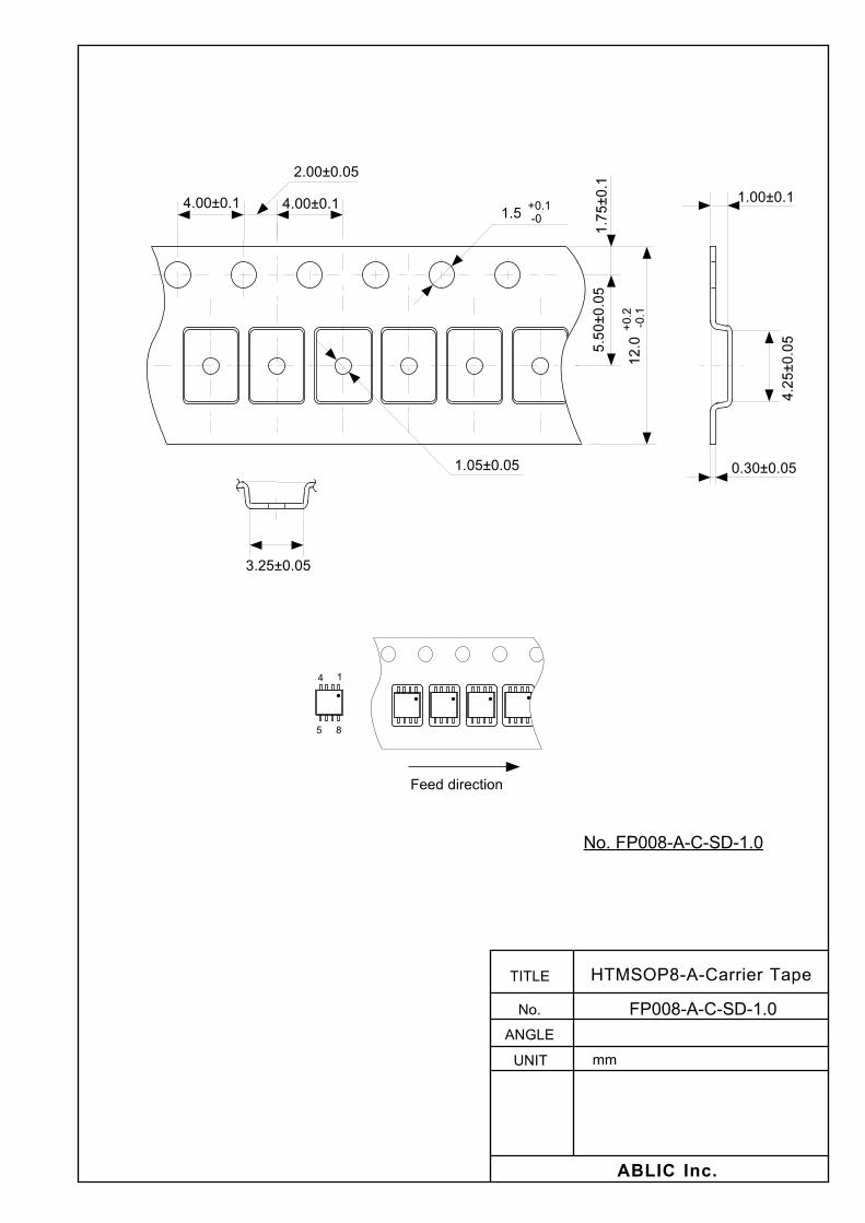
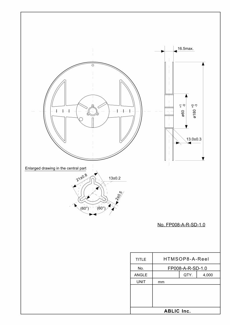
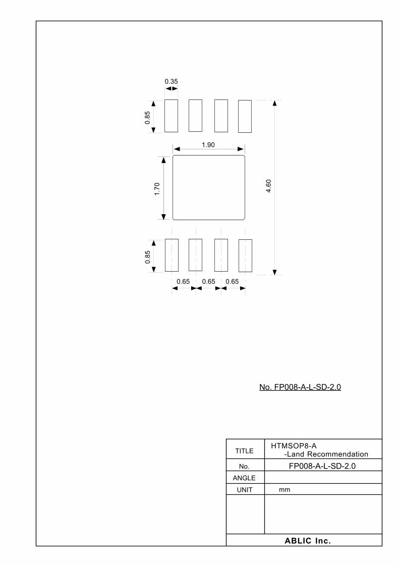
HTMSOP-8 FP008-A-P-SD FP008-A-C-SD FP008-A-R-SD FP008-A-L-SD
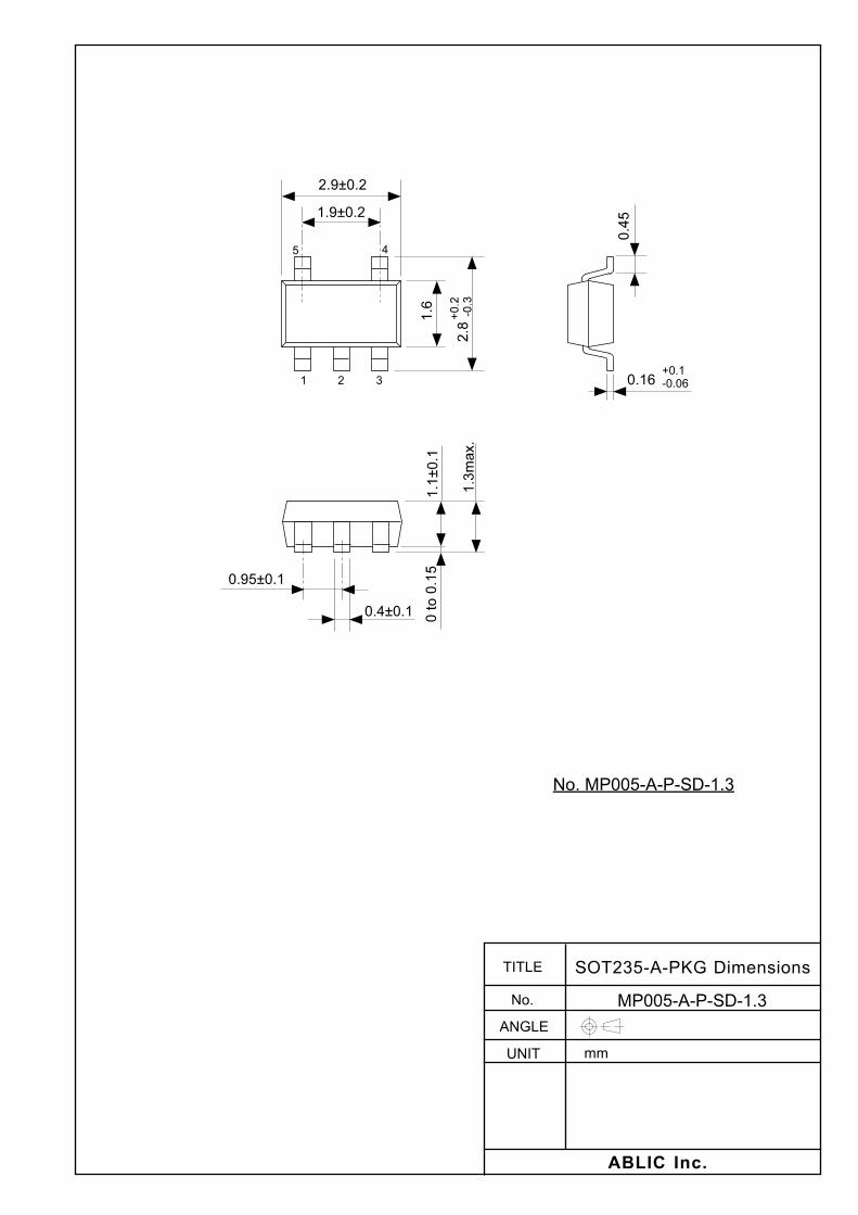
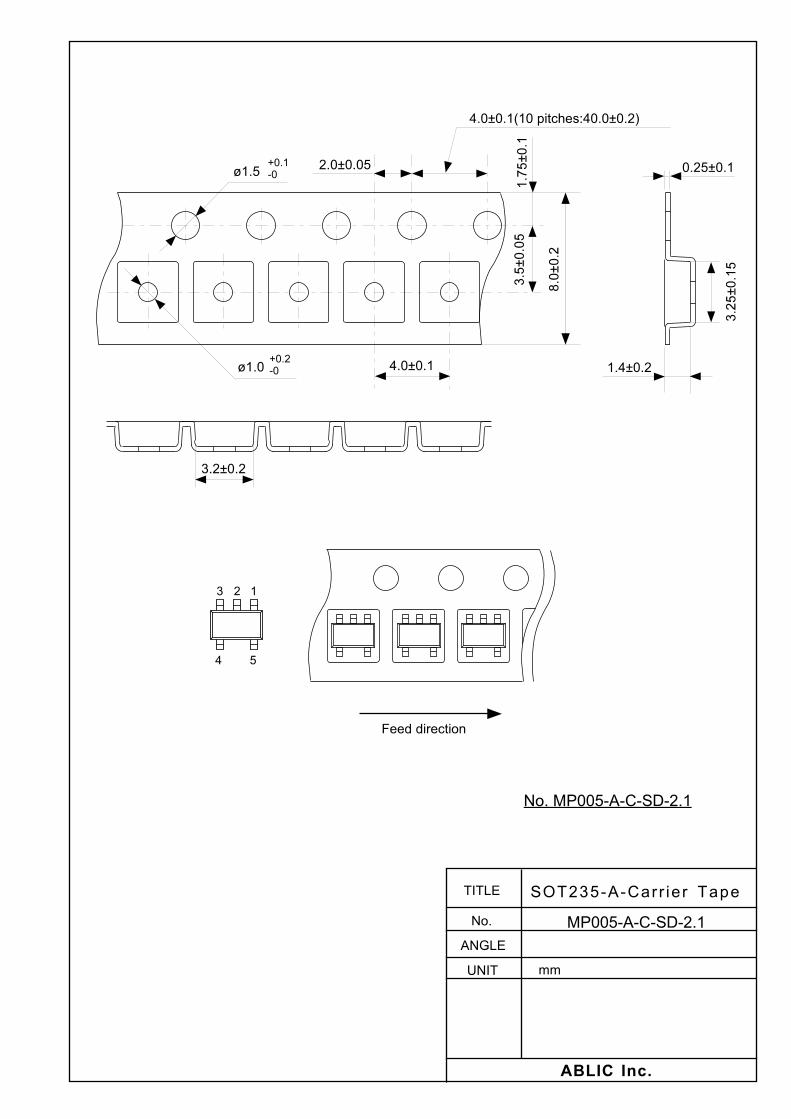
SOT-23-5 MP005-A-P-SD MP005-A-C-SD MP005-A-R-SD −
4. Product name list
4. 1 S-19212B/DxxA Series B type
ON / OFF logic: Active "H" ON / OFF pin input voltage "H" (VSH) = 1.5 V min., ON / OFF pin input voltage "L" (VSL) = 0.25 V max.
Table 3
Output Voltage TO-252-5S(A) HSOP-8A HSOP-6 SOT-89-5 HTMSOP-8 SOT-23-5
2.5 V ± 2.0% S-19212B25A-V5T2U S-19212B25A-E8T1U S-19212B25A-E6T1U S-19212B25A-U5T1U S-19212B25A-S8T1U S-19212B25A-M5T1U
3.0 V ± 2.0% S-19212B30A-V5T2U S-19212B30A-E8T1U S-19212B30A-E6T1U S-19212B30A-U5T1U S-19212B30A-S8T1U S-19212B30A-M5T1U
3.3 V ± 2.0% S-19212B33A-V5T2U S-19212B33A-E8T1U S-19212B33A-E6T1U S-19212B33A-U5T1U S-19212B33A-S8T1U S-19212B33A-M5T1U
5.0 V ± 2.0% S-19212B50A-V5T2U S-19212B50A-E8T1U S-19212B50A-E6T1U S-19212B50A-U5T1U S-19212B50A-S8T1U S-19212B50A-M5T1U
5.5 V ± 2.0% S-19212B55A-V5T2U S-19212B55A-E8T1U S-19212B55A-E6T1U S-19212B55A-U5T1U S-19212B55A-S8T1U S-19212B55A-M5T1U
6.0 V ± 2.0% S-19212B60A-V5T2U S-19212B60A-E8T1U S-19212B60A-E6T1U S-19212B60A-U5T1U S-19212B60A-S8T1U S-19212B60A-M5T1U
7.0 V ± 2.0% S-19212B70A-V5T2U S-19212B70A-E8T1U S-19212B70A-E6T1U S-19212B70A-U5T1U S-19212B70A-S8T1U S-19212B70A-M5T1U
8.0 V ± 2.0% S-19212B80A-V5T2U S-19212B80A-E8T1U S-19212B80A-E6T1U S-19212B80A-U5T1U S-19212B80A-S8T1U S-19212B80A-M5T1U
9.0 V ± 2.0% S-19212B90A-V5T2U S-19212B90A-E8T1U S-19212B90A-E6T1U S-19212B90A-U5T1U S-19212B90A-S8T1U S-19212B90A-M5T1U
10.5 V ± 2.0% S-19212BA5A-V5T2U S-19212BA5A-E8T1U S-19212BA5A-E6T1U S-19212BA5A-U5T1U S-19212BA5A-S8T1U S-19212BA5A-M5T1U
12.0 V ± 2.0% S-19212BC0A-V5T2U S-19212BC0A-E8T1U S-19212BC0A-E6T1U S-19212BC0A-U5T1U S-19212BC0A-S8T1U S-19212BC0A-M5T1U
12.5 V ± 2.0% S-19212BC5A-V5T2U S-19212BC5A-E8T1U S-19212BC5A-E6T1U S-19212BC5A-U5T1U S-19212BC5A-S8T1U S-19212BC5A-M5T1U
15.0 V ± 2.0% S-19212BF0A-V5T2U S-19212BF0A-E8T1U S-19212BF0A-E6T1U S-19212BF0A-U5T1U S-19212BF0A-S8T1U S-19212BF0A-M5T1U
Remark Please contact our sales office for products with specifications other than the above output voltage.
4. 2 S-19212B/DxxA Series D type
ON / OFF logic: Active "H" ON / OFF pin input voltage "H" (VSH) = 2.0 V min., ON / OFF pin input voltage "L" (VSL) = 0.8 V max.
Table 4
Output Voltage TO-252-5S(A) HSOP-8A HSOP-6 SOT-89-5 HTMSOP-8 SOT-23-5
2.5 V ± 2.0% S-19212D25A-V5T2U S-19212D25A-E8T1U S-19212D25A-E6T1U S-19212D25A-U5T1U S-19212D25A-S8T1U S-19212D25A-M5T1U
3.0 V ± 2.0% S-19212D30A-V5T2U S-19212D30A-E8T1U S-19212D30A-E6T1U S-19212D30A-U5T1U S-19212D30A-S8T1U S-19212D30A-M5T1U
3.3 V ± 2.0% S-19212D33A-V5T2U S-19212D33A-E8T1U S-19212D33A-E6T1U S-19212D33A-U5T1U S-19212D33A-S8T1U S-19212D33A-M5T1U
5.0 V ± 2.0% S-19212D50A-V5T2U S-19212D50A-E8T1U S-19212D50A-E6T1U S-19212D50A-U5T1U S-19212D50A-S8T1U S-19212D50A-M5T1U
5.5 V ± 2.0% S-19212D55A-V5T2U S-19212D55A-E8T1U S-19212D55A-E6T1U S-19212D55A-U5T1U S-19212D55A-S8T1U S-19212D55A-M5T1U
6.0 V ± 2.0% S-19212D60A-V5T2U S-19212D60A-E8T1U S-19212D60A-E6T1U S-19212D60A-U5T1U S-19212D60A-S8T1U S-19212D60A-M5T1U
7.0 V ± 2.0% S-19212D70A-V5T2U S-19212D70A-E8T1U S-19212D70A-E6T1U S-19212D70A-U5T1U S-19212D70A-S8T1U S-19212D70A-M5T1U
8.0 V ± 2.0% S-19212D80A-V5T2U S-19212D80A-E8T1U S-19212D80A-E6T1U S-19212D80A-U5T1U S-19212D80A-S8T1U S-19212D80A-M5T1U
9.0 V ± 2.0% S-19212D90A-V5T2U S-19212D90A-E8T1U S-19212D90A-E6T1U S-19212D90A-U5T1U S-19212D90A-S8T1U S-19212D90A-M5T1U
10.5 V ± 2.0% S-19212DA5A-V5T2U S-19212DA5A-E8T1U S-19212DA5A-E6T1U S-19212DA5A-U5T1U S-19212DA5A-S8T1U S-19212DA5A-M5T1U
12.0 V ± 2.0% S-19212DC0A-V5T2U S-19212DC0A-E8T1U S-19212DC0A-E6T1U S-19212DC0A-U5T1U S-19212DC0A-S8T1U S-19212DC0A-M5T1U
12.5 V ± 2.0% S-19212DC5A-V5T2U S-19212DC5A-E8T1U S-19212DC5A-E6T1U S-19212DC5A-U5T1U S-19212DC5A-S8T1U S-19212DC5A-M5T1U
15.0 V ± 2.0% S-19212DF0A-V5T2U S-19212DF0A-E8T1U S-19212DF0A-E6T1U S-19212DF0A-U5T1U S-19212DF0A-S8T1U S-19212DF0A-M5T1U
Remark Please contact our sales office for products with specifications other than the above output voltage.
AUTOMOTIVE, 125°C OPERATION, 36 V INPUT, 250 mA VOLTAGE REGULATORRev.5.2_00 S-19212B/DxxA Series
5
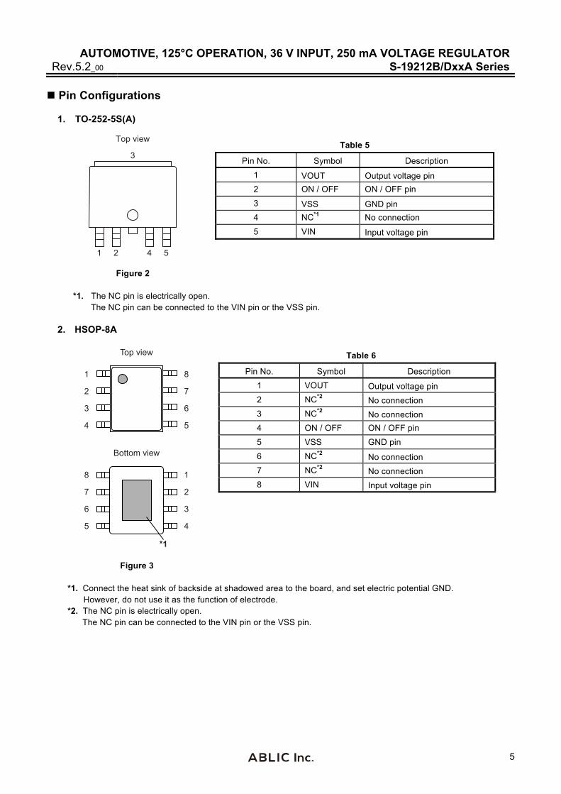
Pin Configurations
1. TO-252-5S(A)
3
Top view
51 42
Figure 2
Table 5
Pin No. Symbol Description
1 VOUT Output voltage pin
2 ON / OFF ON / OFF pin
3 VSS GND pin
4 NC*1 No connection
5 VIN Input voltage pin
*1. The NC pin is electrically open.
The NC pin can be connected to the VIN pin or the VSS pin. 2. HSOP-8A
8
5
6
7
1
4
3
2
Bottom view
Top view
1
4
3
2
8
5
6
7
*1
Figure 3
Table 6
Pin No. Symbol Description
1 VOUT Output voltage pin
2 NC*2 No connection
3 NC*2 No connection
4 ON / OFF ON / OFF pin
5 VSS GND pin
6 NC*2 No connection
7 NC*2 No connection
8 VIN Input voltage pin
*1. Connect the heat sink of backside at shadowed area to the board, and set electric potential GND. However, do not use it as the function of electrode.
*2. The NC pin is electrically open. The NC pin can be connected to the VIN pin or the VSS pin.
AUTOMOTIVE, 125°C OPERATION, 36 V INPUT, 250 mA VOLTAGE REGULATOR S-19212B/DxxA Series Rev.5.2_00
6
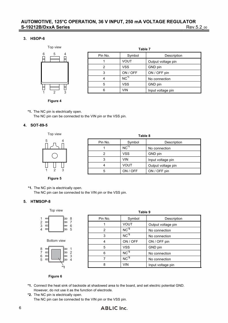
3. HSOP-6
1 32
46 5
Top view
Figure 4
Table 7
Pin No. Symbol Description
1 VOUT Output voltage pin
2 VSS GND pin
3 ON / OFF ON / OFF pin
4 NC*1 No connection
5 VSS GND pin
6 VIN Input voltage pin
*1. The NC pin is electrically open. The NC pin can be connected to the VIN pin or the VSS pin.
4. SOT-89-5
1 32
45
Top view
Figure 5
Table 8
Pin No. Symbol Description
1 NC*1 No connection
2 VSS GND pin
3 VIN Input voltage pin
4 VOUT Output voltage pin
5 ON / OFF ON / OFF pin
*1. The NC pin is electrically open.
The NC pin can be connected to the VIN pin or the VSS pin. 5. HTMSOP-8
Bottom view
1
432
8
567
Top view
8
567
1
432
*1
Figure 6
Table 9
Pin No. Symbol Description
1 VOUT Output voltage pin
2 NC*2 No connection
3 NC*2 No connection
4 ON / OFF ON / OFF pin
5 VSS GND pin
6 NC*2 No connection
7 NC*2 No connection
8 VIN Input voltage pin
*1. Connect the heat sink of backside at shadowed area to the board, and set electric potential GND.
However, do not use it as the function of electrode. *2. The NC pin is electrically open.
The NC pin can be connected to the VIN pin or the VSS pin.
AUTOMOTIVE, 125°C OPERATION, 36 V INPUT, 250 mA VOLTAGE REGULATORRev.5.2_00 S-19212B/DxxA Series
7
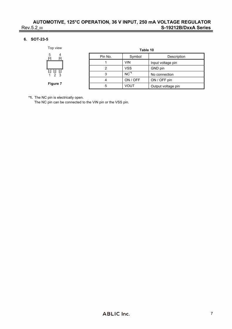
6. SOT-23-5
1 32
45
Top view
Figure 7
Table 10
Pin No. Symbol Description
1 VIN Input voltage pin
2 VSS GND pin
3 NC*1 No connection
4 ON / OFF ON / OFF pin
5 VOUT Output voltage pin
*1. The NC pin is electrically open. The NC pin can be connected to the VIN pin or the VSS pin.
AUTOMOTIVE, 125°C OPERATION, 36 V INPUT, 250 mA VOLTAGE REGULATOR S-19212B/DxxA Series Rev.5.2_00
8
Absolute Maximum Ratings
Table 11 (Ta = +25°C unless otherwise specified)
Item Symbol Absolute Maximum Rating Unit
Input voltage VIN VSS − 0.3 to VSS + 45 V
VON / OFF VSS − 0.3 to VIN + 0.3 ≤ VSS + 45 V
Output voltage VOUT VSS − 0.3 to VIN + 0.3 ≤ VSS + 45 V
Output current IOUT 280 mA
Junction temperature Tj −40 to +150 °C
Operation ambient temperature Topr −40 to +125 °C
Storage temperature Tstg −40 to +150 °C
Caution The absolute maximum ratings are rated values exceeding which the product could suffer physical damage. These values must therefore not be exceeded under any conditions.
Thermal Resistance Value
Table 12
Item Symbol Condition Min. Typ. Max. Unit
Junction-to-ambient thermal resistance*1 θJA
TO-252-5S(A)
Board A − 90 − °C/W
Board B − 58 − °C/W
Board C − 38 − °C/W
Board D − 30 − °C/W
Board E − 29 − °C/W
HSOP-8A
Board A − 115 − °C/W
Board B − 82 − °C/W
Board C − 42 − °C/W
Board D − 43 − °C/W
Board E − 35 − °C/W
HSOP-6
Board A − 106 − °C/W
Board B − 82 − °C/W
Board C − − − °C/W
Board D − 51 − °C/W
Board E − 48 − °C/W
SOT-89-5
Board A − 123 − °C/W
Board B − 90 − °C/W
Board C − − − °C/W
Board D − 53 − °C/W
Board E − 41 − °C/W
HTMSOP-8
Board A − 161 − °C/W
Board B − 116 − °C/W
Board C − 44 − °C/W
Board D − 44 − °C/W
Board E − 35 − °C/W
SOT-23-5
Board A − 180 − °C/W
Board B − 143 − °C/W
Board C − − − °C/W
Board D − − − °C/W
Board E − − − °C/W
*1. Test environment: compliance with JEDEC STANDARD JESD51-2A
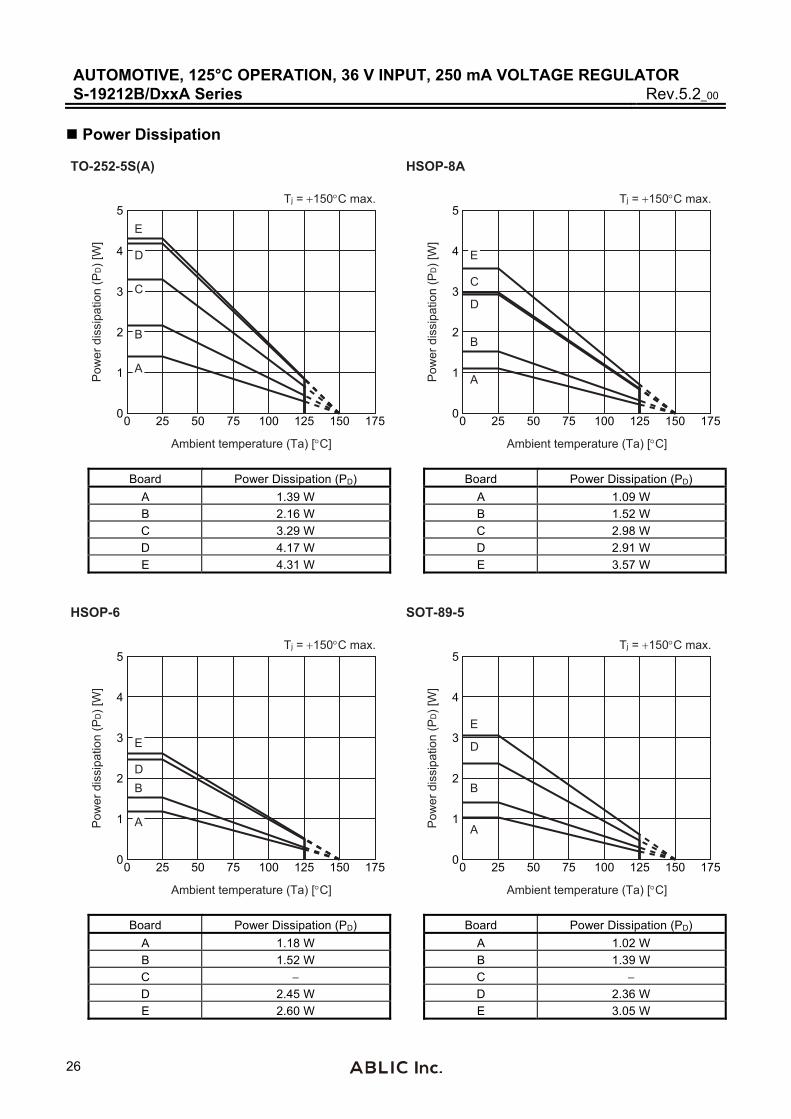
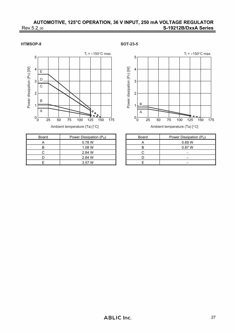
Remark Refer to " Power Dissipation" and "Test Board" for details.
AUTOMOTIVE, 125°C OPERATION, 36 V INPUT, 250 mA VOLTAGE REGULATORRev.5.2_00 S-19212B/DxxA Series
9
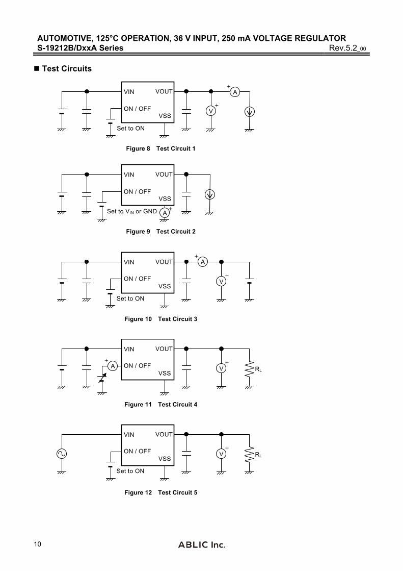
Electrical Characteristics Table 13
(Tj = −40°C to +125°C unless otherwise specified)
Item Symbol Condition Min. Typ. Max. UnitTest
Circuit
Output voltage*1 VOUT(E) VIN = VOUT(S) + 2.0 V, IOUT = 10 mA VOUT(S)
× 0.980VOUT(S)
VOUT(S) × 1.020
V 1
Output current*2 IOUT VIN ≥ VOUT(S) + 2.0 V 250*4 − − mA 3
Dropout voltage*3 Vdrop IOUT = 125 mA, Ta = +25°C − 0.35 − V 1 IOUT = 250 mA, Ta = +25°C − 0.80 − V 1
Line regulation ΔVOUT1
ΔVIN • VOUT VOUT(S) + 0.5 V ≤ VIN ≤ 36 V, IOUT = 10 mA − 0.01 0.03 %/V 1
Load regulation ΔVOUT2
VIN = VOUT(S) + 2.0 V, 2.5 V ≤ VOUT(S) < 5.1 V, 0.1 mA ≤ IOUT ≤ 40 mA
− 16 30 mV 1
VIN = VOUT(S) + 2.0 V, 5.1 V ≤ VOUT(S) < 12.1 V, 0.1 mA ≤ IOUT ≤ 40 mA
− 16 35 mV 1
VIN = VOUT(S) + 2.0 V, 12.1 V ≤ VOUT(S) ≤ 16.0 V, 0.1 mA ≤ IOUT ≤ 40 mA
− 16 40 mV 1
Current consumption during operation
ISS1 VIN = 18.0 V, VON / OFF = VIN, IOUT = 0.01 mA
− 6.5 8.5 μA 2
Current consumption during power-off
ISS2 VIN = 18.0 V, VON / OFF = 0 V, no load
− 0.1 3.5 μA 2
Input voltage VIN − 3.0 − 36 V −
ON / OFF pin input voltage "H"
VSH VIN = 18.0 V, RL = 1.0 kΩ, determined by VOUT output level
B type (ON / OFF logic active "H")
1.5 − − V 4
D type (ON / OFF logic active "H")
2.0 − − V 4
ON / OFF pin input voltage "L"
VSL VIN = 18.0 V, RL = 1.0 kΩ, determined by VOUT output level
B type (ON / OFF logic active "H")
− − 0.25 V 4
D type (ON / OFF logic active "H")
− − 0.8 V 4
ON / OFF pin input current "H"
ISH VIN = 18.0 V, VON / OFF = VIN −0.1 − 0.1 μA 4
ON / OFF pin input current "L"
ISL VIN = 18.0 V, VON / OFF = 0 V −0.1 − 0.1 μA 4
Ripple rejection |RR|
VIN = VOUT(S) + 2.0 V, f = 100 Hz, ΔVrip = 0.5 Vrms, IOUT = 10 mA, Ta = +25°C
2.5 V ≤ VOUT(S) < 3.6 V − 45 − dB 5
3.6 V ≤ VOUT(S) < 6.1 V − 40 − dB 5
6.1 V ≤ VOUT(S) < 10.1 V − 35 − dB 5
10.1 V ≤ VOUT(S) ≤ 16.0 V − 30 − dB 5
Short-circuit current Ishort VIN = VOUT(S) + 2.0 V, VON / OFF = VIN, VOUT = 0 V, Ta = +25°C
− 120 − mA 3
Thermal shutdown detection temperature
TSD Junction temperature − 165 − °C −
Thermal shutdown release temperature
TSR Junction temperature − 140 − °C −
Discharge shunt resistance during power-off
RLOW VIN = 18.0 V, VON / OFF = 0 V, VOUT = 2.0 V − 70 − kΩ 6
*1. VOUT(S): Set output voltage VOUT(E): Actual output voltage
The output voltage when VIN = VOUT(S) + 2.0 V, IOUT = 10 mA *2. The output current at which the output voltage becomes 95% of VOUT(E) after gradually increasing the output current. *3. Vdrop = VIN1 − (VOUT3 × 0.98)
VIN1 is the input voltage at which the output voltage becomes 98% of VOUT3 after gradually decreasing the input voltage. VOUT3 is the output voltage when VIN = VOUT(S) + 2.0 V, and IOUT = 125 mA or 250 mA.
*4. Due to limitation of the power dissipation, this value may not be satisfied. Attention should be paid to the power dissipation when the output current is large. This specification is guaranteed by design.
AUTOMOTIVE, 125°C OPERATION, 36 V INPUT, 250 mA VOLTAGE REGULATOR S-19212B/DxxA Series Rev.5.2_00
10
Test Circuits
+VOUTVIN
VSS
+ V
A
ON / OFF
Set to ON
Figure 8 Test Circuit 1
VOUTVIN
VSSON / OFF
Set to VIN or GND
+A
Figure 9 Test Circuit 2
Set to ON
VOUTVIN
VSS
+ V
+A
ON / OFF
Figure 10 Test Circuit 3
VOUTVIN
VSS
+ VON / OFF
+ A RL
Figure 11 Test Circuit 4
VOUTVIN
VSS
+ V ON / OFF RL
Set to ON
Figure 12 Test Circuit 5
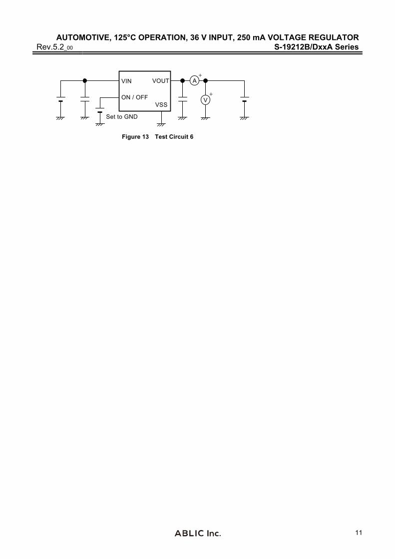
AUTOMOTIVE, 125°C OPERATION, 36 V INPUT, 250 mA VOLTAGE REGULATORRev.5.2_00 S-19212B/DxxA Series
11
Set to GND
VOUTVIN
VSS
+ VON / OFF
+A
Figure 13 Test Circuit 6
AUTOMOTIVE, 125°C OPERATION, 36 V INPUT, 250 mA VOLTAGE REGULATOR S-19212B/DxxA Series Rev.5.2_00
12
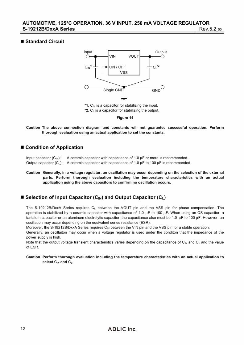
Standard Circuit
CIN*1 CL
*2
Input Output
GNDSingle GND
VOUTVIN
VSS
ON / OFF
*1. CIN is a capacitor for stabilizing the input. *2. CL is a capacitor for stabilizing the output.
Figure 14
Caution The above connection diagram and constants will not guarantee successful operation. Perform thorough evaluation using an actual application to set the constants.
Condition of Application Input capacitor (CIN): A ceramic capacitor with capacitance of 1.0 μF or more is recommended. Output capacitor (CL): A ceramic capacitor with capacitance of 1.0 μF to 100 μF is recommended. Caution Generally, in a voltage regulator, an oscillation may occur depending on the selection of the external
parts. Perform thorough evaluation including the temperature characteristics with an actual application using the above capacitors to confirm no oscillation occurs.
Selection of Input Capacitor (CIN) and Output Capacitor (CL) The S-19212B/DxxA Series requires CL between the VOUT pin and the VSS pin for phase compensation. The operation is stabilized by a ceramic capacitor with capacitance of 1.0 μF to 100 μF. When using an OS capacitor, a tantalum capacitor or an aluminum electrolytic capacitor, the capacitance also must be 1.0 μF to 100 μF. However, an oscillation may occur depending on the equivalent series resistance (ESR). Moreover, the S-19212B/DxxA Series requires CIN between the VIN pin and the VSS pin for a stable operation. Generally, an oscillaiton may occur when a voltage regulator is used under the conditon that the impedance of the power supply is high. Note that the output voltage transient characteristics varies depending on the capacitance of CIN and CL and the value of ESR. Caution Perform thorough evaluation including the temperature characteristics with an actual application to
select CIN and CL.
AUTOMOTIVE, 125°C OPERATION, 36 V INPUT, 250 mA VOLTAGE REGULATORRev.5.2_00 S-19212B/DxxA Series
13
Explanation of Terms
1. Low dropout voltage regulator
This is a voltage regulator which made dropout voltage small by its built-in low on-resistance output transistor.
2. Output voltage (VOUT)
This voltage is output at an accuracy of ±2.0% when the input voltage, the output current and the temperature are in a certain condition*1. *1. Differs depending on the product.
Caution If the certain condition is not satisfied, the output voltage may exceed the accuracy range of ±2.0%. Refer to " Electrical Characteristics" and " Characteristics (Typical Data)" for details.
3. Line regulation
ΔVOUT1
ΔVIN • VOUT
Indicates the dependency of the output voltage against the input voltage. That is, the value shows how much the output voltage changes due to a change in the input voltage after fixing output current constant.
4. Load regulation (ΔVOUT2)
Indicates the dependency of the output voltage against the output current. That is, the value shows how much the output voltage changes due to a change in the output current after fixing input voltage constant.
5. Dropout voltage (Vdrop)
Indicates the difference between input voltage (VIN1) and the output voltage when the output voltage becomes 98% of the output voltage value (VOUT3) at VIN = VOUT(S) + 2.0 V after the input voltage (VIN) is decreased gradually.
Vdrop = VIN1 − (VOUT3 × 0.98)
AUTOMOTIVE, 125°C OPERATION, 36 V INPUT, 250 mA VOLTAGE REGULATOR S-19212B/DxxA Series Rev.5.2_00
14
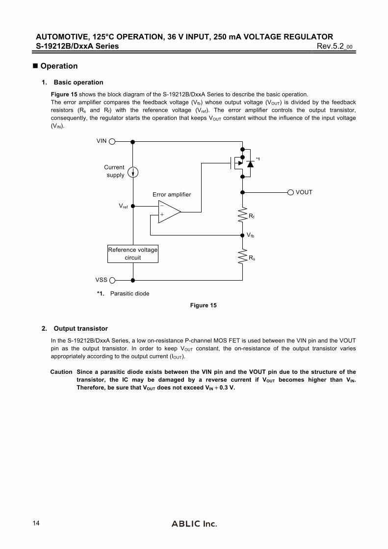
Operation 1. Basic operation
Figure 15 shows the block diagram of the S-19212B/DxxA Series to describe the basic operation. The error amplifier compares the feedback voltage (Vfb) whose output voltage (VOUT) is divided by the feedback resistors (Rs and Rf) with the reference voltage (Vref). The error amplifier controls the output transistor, consequently, the regulator starts the operation that keeps VOUT constant without the influence of the input voltage (VIN).
VOUT
*1
VSS
VIN
Rs
Rf
Error amplifier
Current supply
Vref
Vfb
−+
Reference voltage circuit
*1. Parasitic diode
Figure 15
2. Output transistor
In the S-19212B/DxxA Series, a low on-resistance P-channel MOS FET is used between the VIN pin and the VOUT pin as the output transistor. In order to keep VOUT constant, the on-resistance of the output transistor varies appropriately according to the output current (IOUT). Caution Since a parasitic diode exists between the VIN pin and the VOUT pin due to the structure of the transistor, the IC may be damaged by a reverse current if VOUT becomes higher than VIN. Therefore, be sure that VOUT does not exceed VIN + 0.3 V.
AUTOMOTIVE, 125°C OPERATION, 36 V INPUT, 250 mA VOLTAGE REGULATORRev.5.2_00 S-19212B/DxxA Series
15
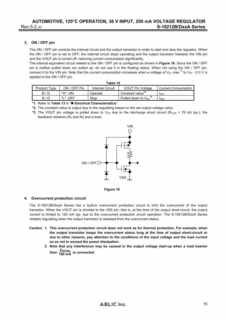
3. ON / OFF pin
The ON / OFF pin controls the internal circuit and the output transistor in order to start and stop the regulator. When the ON / OFF pin is set to OFF, the internal circuit stops operating and the output transistor between the VIN pin and the VOUT pin is turned off, reducing current consumption significantly. The internal equivalent circuit related to the ON / OFF pin is configured as shown in Figure 16. Since the ON / OFF pin is neither pulled down nor pulled up, do not use it in the floating status. When not using the ON / OFF pin, connect it to the VIN pin. Note that the current consumption increases when a voltage of VSL max.*1 to VIN − 0.3 V is applied to the ON / OFF pin.
Table 14
Product Type ON / OFF Pin Internal Circuit VOUT Pin Voltage Current Consumption
B / D "H": ON Operate Constant value*2 ISS1
B / D "L": OFF Stop Pulled down to VSS*3 ISS2
*1. Refer to Table 13 in " Electrical Characteristics". *2. The constant value is output due to the regulating based on the set output voltage value. *3. The VOUT pin voltage is pulled down to VSS due to the discharge shunt circuit (RLOW = 70 kΩ typ.), the
feedback resistors (Rs and Rf) and a load.
VSS
ON / OFF
VIN
Figure 16
4. Overcurrent protection circuit
The S-19212B/DxxA Series has a built-in overcurrent protection circuit to limit the overcurrent of the output transistor. When the VOUT pin is shorted to the VSS pin, that is, at the time of the output short-circuit, the output current is limited to 120 mA typ. due to the overcurrent protection circuit operation. The S-19212B/DxxA Series restarts regulating when the output transistor is released from the overcurrent status. Caution 1. This overcurrent protection circuit does not work as for thermal protection. For example, when the output transistor keeps the overcurrent status long at the time of output short-circuit or due to other reasons, pay attention to the conditions of the input voltage and the load current so as not to exceed the power dissipation. 2. Note that any interference may be caused in the output voltage start-up when a load heavier
than VOUT(S)
100 mA is connected.
AUTOMOTIVE, 125°C OPERATION, 36 V INPUT, 250 mA VOLTAGE REGULATOR S-19212B/DxxA Series Rev.5.2_00
16
5. Thermal shutdown circuit
The S-19212B/DxxA Series has a built-in thermal shutdown circuit to limit overheating. When the junction temperature increases to 165°C typ., the thermal shutdown circuit becomes the detection status, and the regulating is stopped. When the junction temperature decreases to 140°C typ., the thermal shutdown circuit becomes the release status, and the regulator is restarted. If the thermal shutdown circuit becomes the detection status due to self-heating, the regulating is stopped and VOUT decreases. For this reason, the self-heating is limited and the temperature of the IC decreases. The thermal shutdown circuit becomes release status when the temperature of the IC decreases, and the regulating is restarted, thus the self-heating is generated again. Repeating this procedure makes the waveform of VOUT into a pulse-like form. This phenomenon continues unless decreasing either or both of the input voltage and the output current in order to reduce the internal power consumption, or decreasing the ambient temperature. Note that the product may suffer physical damage such as deterioration if the above phenomenon occurs continuously. Caution 1. When the heat radiation of the application is not in a good condition, the self-heating cannot be
limited immediately, and the IC may suffer physical damage. Perform thorough evaluation including the temperature characteristics with an actual application to confirm no problems happen.
2. If a large load current flows during the restart process of regulating after the thermal shutdown
circuit changes to the release status from the detection status, the thermal shutdown circuit becomes the detection status again due to self-heating, and a problem may happen in the restart of regulating. A large load current, for example, occurs when charging to the CL whose capacitance is large.
Perform thorough evaluation including the temperature characteristics with an actual application to select CL.
Table 15
Thermal Shutdown Circuit VOUT Pin Voltage
Release: 140°C typ.*1 Constant value*2
Detection: 165°C typ.*1 Pulled down to VSS*3
*1. Junction temperature *2. The constant value is output due to the regulating based on the set output voltage value. *3. The VOUT pin voltage is pulled down to VSS due to the feedback resistors (Rs and Rf) and a load.
AUTOMOTIVE, 125°C OPERATION, 36 V INPUT, 250 mA VOLTAGE REGULATORRev.5.2_00 S-19212B/DxxA Series
17
Precautions • Generally, when a voltage regulator is used under the condition that the load current value is small (0.1 mA or less),
the output voltage may increase due to the leakage current of an output transistor.
• Generally, when a voltage regulator is used under the condition that the temperature is high, the output voltage may increase due to the leakage current of an output transistor.
• Generally, when the ON / OFF pin is used under the condition of OFF, the output voltage may increase due to the leakage current of an output transistor.
• Generally, when a voltage regulator is used under the condition that the impedance of the power supply is high, an oscillation may occur. Perform thorough evaluation including the temperature characteristics with an actual application to select CIN.
• Generally, in a voltage regulator, an oscillation may occur depending on the selection of the external parts. The following use conditions are recommended in the S-19212B/DxxA Series, however, perform thorough evaluation including the temperature characteristics with an actual application to select CIN and CL.
Input capacitor (CIN): A ceramic capacitor with capacitance of 1.0 μF or more is recommended. Output capacitor (CL): A ceramic capacitor with capacitance of 1.0 μF to 100 μF is recommended.
• Generally, in a voltage regulator, the values of an overshoot and an undershoot in the output voltage vary depending on the variation factors of input voltage start-up, input voltage fluctuation and load fluctuation etc., or the capacitance of CIN or CL and the value of the equivalent series resistance (ESR), which may cause a problem to the stable operation. Perform thorough evaluation including the temperature characteristics with an actual application to select CIN and CL.
• Generally, in a voltage regulator, an overshoot may occur in the output voltage momentarily if the input voltage steeply changes when the input voltage is started up or the input voltage fluctuates etc. Perform thorough evaluation including the temperature characteristics with an actual application to confirm no problems happen.
• Generally, in a voltage regulator, if the VOUT pin is steeply shorted with GND, a negative voltage exceeding the absolute maximum ratings may occur in the VOUT pin due to resonance phenomenon of the inductance and the capacitance including CL on the application. The resonance phenomenon is expected to be weakened by inserting a series resistor into the resonance path, and the negative voltage is expected to be limited by inserting a protection diode between the VOUT pin and the VSS pin.
• If the input voltage is started up steeply under the condition that the capacitance of CL is large, the thermal shutdown circuit may be in the detection status by self-heating due to the charge current to CL.
• Make sure of the conditions for the input voltage, output voltage and the load current so that the internal loss does not exceed the power dissipation.
• Do not apply an electrostatic discharge to this IC that exceeds the performance ratings of the built-in electrostatic protection circuit.
• When considering the output current value that the IC is able to output, make sure of the output current value specified in Table 13 in " Electrical Characteristics" and footnote *4 of the table.
• Wiring patterns on the application related to the VIN pin, the VOUT pin and the VSS pin should be designed so that the impedance is low. When mounting CIN between the VIN pin and the VSS pin and CL between the VOUT pin and the VSS pin, connect the capacitors as close as possible to the respective destination pins of the IC.
• In the package equipped with heat sink of backside, mount the heat sink firmly. Since the heat radiation differs according to the condition of the application, perform thorough evaluation with an actual application to confirm no problems happen.
• ABLIC Inc. claims no responsibility for any disputes arising out of or in connection with any infringement by products including this IC of patents owned by a third party.
AUTOMOTIVE, 125°C OPERATION, 36 V INPUT, 250 mA VOLTAGE REGULATOR S-19212B/DxxA Series Rev.5.2_00
18
Characteristics (Typical Data)
1. Output voltage vs. Output current (When load current increases) (Ta = +25°C)
1. 1 VOUT = 2.5 V 1. 2 VOUT = 5.0 V
100 200 300 400 500 600 700 8000
3.0
1.51.00.5
2.02.5
0.0
VO
UT
[V]
IOUT [mA]
VIN = 3.0 V
VIN = 4.5 VVIN = 3.5 V
VIN = 9.0 V
100 200 300 400 500 600 700 8000
6.0
3.02.01.0
4.05.0
0.0
VO
UT
[V]
IOUT [mA]
VIN = 5.5 V
VIN = 7.0 VVIN = 6.0 V
VIN = 9.0 V
Remark In determining the output current, attention should be paid to the following.
1. The minimum output current value and footnote *4 of Table 13 in " Electrical Characteristics" 2. Power dissipation
2. Output voltage vs. Input voltage (Ta = +25°C)
2. 1 VOUT = 2.5 V 2. 2 VOUT = 5.0 V
6 12 18 24 30 360
2.9
1.7
VO
UT
[V]
VIN [V]
2.3
1.9
2.5
2.1
2.7
IOUT = 0.1 mAIOUT = 10 mAIOUT = 40 mA
6 12 18 24 30 360
5.4
4.2
VO
UT
[V]
VIN [V]
4.8
4.4
5.0
4.6
5.2
IOUT = 0.1 mAIOUT = 10 mAIOUT = 40 mA
2. 3 VOUT = 16.0 V
6 12 18 24 30 360
16.4
15.2
VO
UT
[V]
VIN [V]
15.8
15.4
16.0
15.6
16.2
IOUT = 0.1 mAIOUT = 10 mAIOUT = 40 mA
AUTOMOTIVE, 125°C OPERATION, 36 V INPUT, 250 mA VOLTAGE REGULATORRev.5.2_00 S-19212B/DxxA Series
19
3. Dropout voltage vs. Output current
3. 1 VOUT = 2.5 V 3. 2 VOUT = 5.0 V
50 100 150 200 2500
Vdr
op [V
]
IOUT [mA]
1.2
0.0
0.6
0.2
0.8
0.4
1.0
Tj = +125C Tj = +150C
Tj = +25C
Tj = 40C
50 100 150 200 2500
Vdr
op [V
]
IOUT [mA]
1.2
0.0
0.6
0.2
0.8
0.4
1.0
Tj = +125C Tj = +150C
Tj = +25C
Tj = 40C
3. 3 VOUT = 16.0 V
50 100 150 200 2500
Vdr
op [V
]
IOUT [mA]
1.2
0.0
0.6
0.2
0.8
0.4
1.0
Tj = +125C Tj = +150C
Tj = +25C
Tj = 40C
4. Dropout voltage vs. Junction temperature
4. 1 VOUT = 2.5 V 4. 2 VOUT = 5.0 V
−25 0 150125100755025−400.0
0.6
Vdr
op [V
]
0.50.40.30.20.1
Tj [C]
IOUT = 10 mA
IOUT = 125 mA
−25 0 150125100755025−400.0
0.6
Vdr
op [V
]
0.50.40.30.20.1
Tj [C]
IOUT = 10 mA
IOUT = 125 mA
4. 3 VOUT = 16.0 V
−25 0 150125100755025−400.0
0.6
Vdr
op [V
]
0.50.40.30.20.1
Tj [C]
IOUT = 10 mA
IOUT = 125 mA
AUTOMOTIVE, 125°C OPERATION, 36 V INPUT, 250 mA VOLTAGE REGULATOR S-19212B/DxxA Series Rev.5.2_00
20
5. Dropout voltage vs. Set output voltage (Ta = +25°C)
4.0 8.0 12.0 16.00.0
1.0
0.0
VOUT(S) [V]
0.8
0.6
0.4
0.2
Vdr
op [V
]
IOUT = 0.1 mAIOUT = 10 mA
IOUT = 40 mAIOUT = 125 mA IOUT = 250 mA
6. Output voltage vs. Junction temperature
6. 1 VOUT = 2.5 V VIN = 4.5 V
6. 2 VOUT = 5.0 V VIN = 7.0 V
−25 0 150125100755025−402.45
2.55
Tj [C]
2.53
2.51
2.49
2.47
VO
UT
[V]
−25 0 150125100755025−404.90
5.10
Tj [C]
5.06
5.02
4.98
4.94
VO
UT
[V]
6. 3 VOUT = 16.0 V VIN = 18.0 V
−25 0 150125100755025−404.90
5.10
Tj [C]
5.06
5.02
4.98
4.94
VO
UT
[V]
AUTOMOTIVE, 125°C OPERATION, 36 V INPUT, 250 mA VOLTAGE REGULATORRev.5.2_00 S-19212B/DxxA Series
21
7. Current consumption during operation vs. Input voltage (When ON / OFF pin is ON, no load)
7. 1 VOUT = 2.5 V 7. 2 VOUT = 5.0 V
6 12 18 24 30 360
50.0
0.0
ISS
1 [A
]
VIN [V]
40.0
30.0
20.0
10.0
Tj = 125C Tj = 150C
Tj = 25C Tj = 40C
6 12 18 24 30 360
50.0
0.0
ISS
1 [A
]
VIN [V]
40.0
30.0
20.0
10.0
Tj = 125C Tj = 150C
Tj = 25C Tj = 40C
7. 3 VOUT = 16.0 V
6 12 18 24 30 360
50.0
0.0
ISS
1 [A
]
VIN [V]
40.0
30.0
20.0
10.0
Tj = 125C Tj = 150C
Tj = 25C Tj = 40C
8. Current consumption during operation vs. Junction temperature
8. 1 VOUT = 2.5 V VIN = 18.0 V
8. 2 VOUT = 5.0 V VIN = 18.0 V
25 50 75 100 125 1500
10.0
0.0
Tj [C]
8.0
6.0
4.0
2.0
ISS
1 [A
]
25 50 75 100 125 1500
10.0
0.0
Tj [C]
8.0
6.0
4.0
2.0
ISS
1 [A
]
8. 3 VOUT = 16.0 V VIN = 18.0 V
25 50 75 100 125 1500
10.0
0.0
Tj [C]
8.0
6.0
4.0
2.0
ISS
1 [A
]
AUTOMOTIVE, 125°C OPERATION, 36 V INPUT, 250 mA VOLTAGE REGULATOR S-19212B/DxxA Series Rev.5.2_00
22
9. Current consumption during operation vs. Output current (Ta = +25°C)
9. 1 VOUT = 2.5 V 9. 2 VOUT = 5.0 V
50 100 150 200 2500
50.0
0.0
40.0
30.0
20.0
10.0
ISS
1 [A
]
IOUT [mA]
VIN = 13.5 V
VIN = 3.5 V
50 100 150 200 2500
50.0
0.0
40.0
30.0
20.0
10.0
ISS
1 [A
]
IOUT [mA]
VIN = 13.5 V
VIN = 6.0 V
9. 3 VOUT = 16.0 V
50 100 150 200 2500
50.0
0.0
40.0
30.0
20.0
10.0
ISS
1 [A
]
IOUT [mA]
VIN = 20.0 V
VIN = 17.0 V
10. Ripple rejection (Ta = +25°C)
10. 1 VOUT = 2.5 V VIN = 4.5 V, CL = 1.0 μF
10. 2 VOUT = 5.0 V VIN = 7.0 V, CL = 1.0 μF
Rip
ple
Rej
ectio
n [d
B]
Frequency [Hz]10 100k
0
120
10k1k100
604020
80100
IOUT = 10 mA
IOUT = 250 mA
IOUT = 0.01 mA
Rip
ple
Rej
ectio
n [d
B]
Frequency [Hz]10 100k
0
120
10k1k100
604020
80100
IOUT = 10 mA
IOUT = 250 mA
IOUT = 0.01 mA
10. 3 VOUT = 16.0 V
VIN = 18.0 V, CL = 1.0 μF
Rip
ple
Rej
ectio
n [d
B]
Frequency [Hz]10 100k
0
120
10k1k100
604020
80100
IOUT = 10 mA
IOUT = 250 mA
IOUT = 0.01 mA
AUTOMOTIVE, 125°C OPERATION, 36 V INPUT, 250 mA VOLTAGE REGULATORRev.5.2_00 S-19212B/DxxA Series
23
Reference Data
1. Characteristics of input transient response (Ta = +25°C)
1. 1 VOUT = 2.5 V IOUT = 40 mA, CIN = 1.0 μF, VIN = 11.5 V ↔ 13.5 V, tr = tf = 5.0 μs
1. 2 VOUT = 5.0 V IOUT = 40 mA, CIN = 1.0 μF, VIN = 11.5 V ↔ 13.5 V, tr = tf = 5.0 μs
VO
UT
[V]
t [ms]V
IN [V
]
3.3
2.3
15
50.0 0.4 0.8 1.2 1.6 2.0 2.4 2.80.4
3.1
2.9
2.7
2.5
13
11
9
7
CL = 10.0 FVIN
VOUT
CL = 22.0 F VO
UT
[V]
t [ms]
VIN
[V]
5.8
4.8
15
50.0 0.4 0.8 1.2 1.6 2.0 2.4 2.80.4
5.6
5.4
5.2
5.0
13
11
9
7
CL = 10.0 FVIN
VOUT
CL = 22.0 F
1. 3 VOUT = 16.0 V IOUT = 40 mA, CIN = 1.0 μF, VIN = 18.0 V ↔ 19.5 V, tr = tf = 5.0 μs
VO
UT
[V]
t [ms]
VIN
[V]
16.8
15.8
21
110.0 0.4 0.8 1.2 1.6 2.0 2.4 2.80.4
16.6
16.4
16.2
16.0
19
17
15
13
CL = 10.0 FVIN
VOUT
CL = 22.0 F
2. Characteristics of load transient response (Ta = +25°C)
2. 1 VOUT = 2.5 V VIN = 13.5 V, CIN = 1.0 μF, IOUT = 50 mA ↔ 100 mA
2. 2 VOUT = 5.0 V VIN = 13.5 V, CIN = 1.0 μF, IOUT = 50 mA ↔ 100 mA
VO
UT
[V]
t [ms]
2.9
2.3
150
1500.0 0.4 0.8 1.2 1.6 2.0 2.4 2.80.4
2.6
2.4
2.7
2.5
2.8
0
100
50
50
100
IOU
T [m
A]
CL = 10.0 F
IOUT
VOUT
CL = 22.0 F
VO
UT
[V]
t [ms]
5.4
4.8
150
1500.0 0.4 0.8 1.2 1.6 2.0 2.4 2.80.4
5.1
4.9
5.2
5.0
5.3
0
100
50
50
100
IOU
T [m
A]
CL = 10.0 F
IOUT
VOUT
CL = 22.0 F
2. 3 VOUT = 16.0 V VIN = 18.0 V, CIN = 1.0 μF, IOUT = 50 mA ↔ 100 mA
VO
UT
[V]
t [ms]
16.4
15.8
150
1500.0 0.4 0.8 1.2 1.6 2.0 2.4 2.80.4
16.1
15.9
16.2
16.0
16.3
0
100
50
50
100
IOU
T [m
A]
CL = 10.0 F
IOUT
VOUT
CL = 22.0 F
AUTOMOTIVE, 125°C OPERATION, 36 V INPUT, 250 mA VOLTAGE REGULATOR S-19212B/DxxA Series Rev.5.2_00
24
3. Transient response characteristics of ON / OFF pin (Ta = +25°C)
3. 1 VOUT = 2.5 V VIN = 13.5 V, CL = 10.0 μF, CIN = 1.0 μF, IOUT = 125 mA, VON / OFF = 0 V → 13.5 V
3. 2 VOUT = 5.0 V VIN = 13.5 V, CL = 10.0 μF, CIN = 1.0 μF, IOUT = 125 mA, VON / OFF = 0 V → 13.5 V
VO
N /
OFF
[V]
t [ms]
6.0
0.0
9.0
3.0
12.015.0
3.0
6
0612
1218
180.0 0.50.5 1.51.0 2.0 2.5 3.0
VO
UT
[V]
VOUT
VON / OFF
VO
N /
OFF
[V]
t [ms]
6.0
0.0
9.0
3.0
12.015.0
3.0
6
0612
1218
180.0 0.50.5 1.51.0 2.0 2.5 3.0
VO
UT
[V]
VOUT
VON / OFF
4. Load transient response characteristics dependent on capacitance (Ta = +25°C)
4. 1 VOUT = 5.0 V VIN = 13.5 V, CIN = 1.0 μF, IOUT = 50 mA → 100 mA
VIN = 13.5 V, CIN = 1.0 μF, IOUT = 100 mA → 50 mA
20 40 60 80 1000
0.20
Und
ersh
oot [
V]
CL [F]
0.15
0.10
0.05
0.0020 40 60 80 1000
0.20
Ove
rsho
ot [V
]
CL [F]
0.15
0.10
0.05
0.00
5. Input transient response characteristics dependent on capacitance (Ta = +25°C)
5. 1 VOUT = 5.0 V VIN = 7.0 V → 12.0 V, tr = 5.0 μs,
CIN = 1.0 μF, IOUT = 40 mA
VIN = 12.0 V → 7.0 V, tr = 5.0 μs,
CIN = 1.0 μF, IOUT = 40 mA
20 40 60 80 1000
2.0
Ove
rsho
ot [V
]
CL [μF]
1.5
1.0
0.5
0.020 40 60 80 1000
2.0
Und
ersh
oot [
V]
CL [μF]
1.5
1.0
0.5
0.0
AUTOMOTIVE, 125°C OPERATION, 36 V INPUT, 250 mA VOLTAGE REGULATORRev.5.2_00 S-19212B/DxxA Series
25
6. Load dump characteristics (Ta = +25°C)
6. 1 VOUT = 3.3 V
IOUT = 0.1 mA, VIN = 13.5 V ↔ 45.0 V, CIN = CL = 1.0 μF
4.3
3.10.1 0.9
VO
UT
[V]
0.40.30.20.10
4.13.93.73.53.3
t [s]
50
10
403020100
VIN
[V]
0.5 0.6 0.7 0.8
VOUT
VIN
7. Example of equivalent series resistance vs. Output current characteristics (Ta = +25°C)
100
0.1 250IOUT [mA]
RE
SR [
Ω]
CIN = CL = 1.0 μF
0
Stable
CIN
VIN
VSS
CL*1
RESR
S-19212B/DxxA Series
VOUT
ON / OFF
*1. CL: TDK Corporation CGA5L3X8R1H105M (1.0 μF)
Figure 17 Figure 18
AUTOMOTIVE, 125°C OPERATION, 36 V INPUT, 250 mA VOLTAGE REGULATOR S-19212B/DxxA Series Rev.5.2_00
26
Power Dissipation
0 25 50 75 100 125 150 1750
1
2
3
4
5
Ambient temperature (Ta) [C]
Pow
er d
issi
patio
n (P
D) [
W]
Tj = 150C max.
TO-252-5S(A)
E
D
C
B
A
0 25 50 75 100 125 150 1750
1
2
3
4
5
Ambient temperature (Ta) [C]P
ower
dis
sipa
tion
(PD) [
W]
Tj = 150C max.
HSOP-8A
E
D
C
B
A
Board Power Dissipation (PD) Board Power Dissipation (PD)
A 1.39 W A 1.09 W
B 2.16 W B 1.52 W
C 3.29 W C 2.98 W D 4.17 W D 2.91 W
E 4.31 W E 3.57 W
0 25 50 75 100 125 150 1750
1
2
3
4
5
Ambient temperature (Ta) [C]
Pow
er d
issi
patio
n (P
D) [
W]
Tj = 150C max.
HSOP-6
E
DB
A
0 25 50 75 100 125 150 1750
1
2
3
4
5
Ambient temperature (Ta) [C]
Pow
er d
issi
patio
n (P
D) [
W]
Tj = 150C max.
SOT-89-5
E
D
B
A
Board Power Dissipation (PD) Board Power Dissipation (PD)
A 1.18 W A 1.02 W
B 1.52 W B 1.39 W
C − C −
D 2.45 W D 2.36 W
E 2.60 W E 3.05 W
AUTOMOTIVE, 125°C OPERATION, 36 V INPUT, 250 mA VOLTAGE REGULATORRev.5.2_00 S-19212B/DxxA Series
27
0 25 50 75 100 125 150 1750
1
2
3
4
5
Ambient temperature (Ta) [C]
Pow
er d
issi
patio
n (P
D) [
W]
Tj = 150C max.
HTMSOP-8
E
D
C
B
A
0 25 50 75 100 125 150 1750
1
2
3
4
5
Ambient temperature (Ta) [C]P
ower
dis
sipa
tion
(PD) [
W]
Tj = 150C max.
SOT-23-5
B
A
Board Power Dissipation (PD) Board Power Dissipation (PD)
A 0.78 W A 0.69 W
B 1.08 W B 0.87 W
C 2.84 W C − D 2.84 W D − E 3.57 W E −
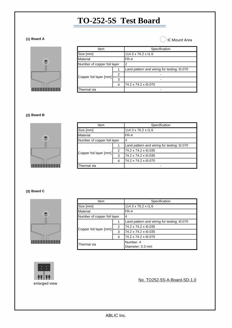
(1)
1234
(2)
1234
(3)
1234
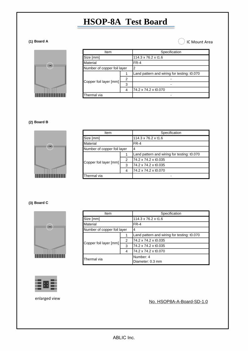
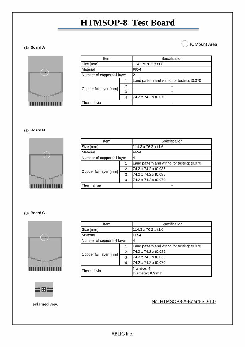
Board C
Item Specification
Material FR-4Number of copper foil layer 4
Copper foil layer [mm]
Land pattern and wiring for testing: t0.07074.2 x 74.2 x t0.03574.2 x 74.2 x t0.03574.2 x 74.2 x t0.070
Thermal via Number: 4Diameter: 0.3 mm
Board B
Item Specification
Size [mm] 114.3 x 76.2 x t1.6
Material FR-4Number of copper foil layer 4
Copper foil layer [mm]
Land pattern and wiring for testing: t0.07074.2 x 74.2 x t0.03574.2 x 74.2 x t0.03574.2 x 74.2 x t0.070
Thermal via -
Size [mm] 114.3 x 76.2 x t1.6
Number of copper foil layer 2
Copper foil layer [mm]
Land pattern and wiring for testing: t0.070--
74.2 x 74.2 x t0.070Thermal via -
Material FR-4
Board A
Item SpecificationSize [mm] 114.3 x 76.2 x t1.6
IC Mount Area
enlarged view
TO-252-5S Test Board
No. TO252-5S-A-Board-SD-1.0
ABLIC Inc.
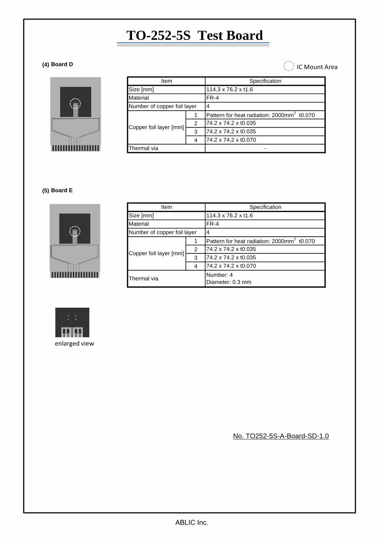
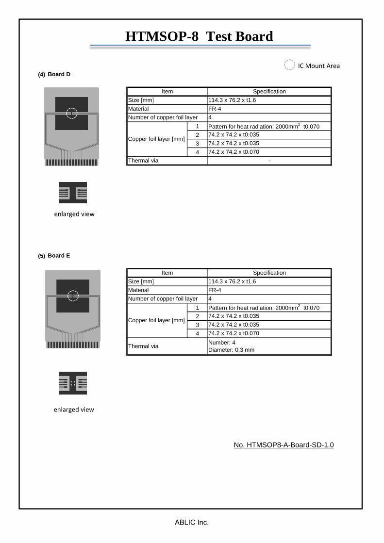
(4)
1234
(5)
1234
Thermal via Number: 4Diameter: 0.3 mm
Material FR-4Number of copper foil layer 4
Copper foil layer [mm]
Pattern for heat radiation: 2000mm2 t0.07074.2 x 74.2 x t0.03574.2 x 74.2 x t0.03574.2 x 74.2 x t0.070
Thermal via -
Board E
Item SpecificationSize [mm] 114.3 x 76.2 x t1.6
Number of copper foil layer 4
Copper foil layer [mm]
Pattern for heat radiation: 2000mm2 t0.07074.2 x 74.2 x t0.03574.2 x 74.2 x t0.03574.2 x 74.2 x t0.070
Board D
Item SpecificationSize [mm] 114.3 x 76.2 x t1.6Material FR-4
enlarged view
IC Mount Area
TO-252-5S Test Board
No. TO252-5S-A-Board-SD-1.0
ABLIC Inc.
(1)
1234
(2)
1234
(3)
1234
Board A
Board B
Board C
Thermal via Number: 4Diameter: 0.3 mm
Number of copper foil layer 4
Copper foil layer [mm]
Land pattern and wiring for testing: t0.07074.2 x 74.2 x t0.03574.2 x 74.2 x t0.03574.2 x 74.2 x t0.070
Material FR-4
Thermal via -
Item Specification
Copper foil layer [mm]
Land pattern and wiring for testing: t0.07074.2 x 74.2 x t0.03574.2 x 74.2 x t0.03574.2 x 74.2 x t0.070
Size [mm] 114.3 x 76.2 x t1.6
Size [mm] 114.3 x 76.2 x t1.6Material FR-4Number of copper foil layer 4
Copper foil layer [mm]
Land pattern and wiring for testing: t0.070--
Item Specification
74.2 x 74.2 x t0.070
Size [mm] 114.3 x 76.2 x t1.6Item Specification
Thermal via -
Material FR-4Number of copper foil layer 2
IC Mount Area
enlarged view
HSOP-8A Test Board
No. HSOP8A-A-Board-SD-1.0
ABLIC Inc.
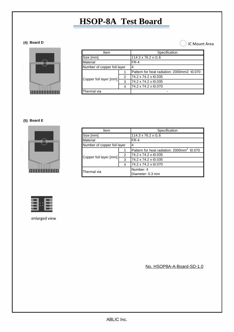
(4)
1234
(5)
1234
Size [mm] 114.3 x 76.2 x t1.6Material FR-4
Item Specification
Number of copper foil layer 4
Copper foil layer [mm]
Pattern for heat radiation: 2000mm2 t0.07074.2 x 74.2 x t0.03574.2 x 74.2 x t0.03574.2 x 74.2 x t0.070
74.2 x 74.2 x t0.070
Size [mm] 114.3 x 76.2 x t1.6Material FR-4
Thermal via -
Item Specification
Board D
Board E
Thermal via Number: 4Diameter: 0.3 mm
Number of copper foil layer 4
Copper foil layer [mm]
Pattern for heat radiation: 2000mm2 t0.07074.2 x 74.2 x t0.03574.2 x 74.2 x t0.035
enlarged view
IC Mount Area
HSOP-8A Test Board
No. HSOP8A-A-Board-SD-1.0
ABLIC Inc.
(1)Item Specification
Size [mm] 114.3 x 76.2 x t1.6Material FR-4Number of copper foil layer 2Copper foil layer [mm] 1 Land pattern and wiring for testing: t0.070
2 -3 -4 74.2 x 74.2 x t0.070
(2)Item Specification
Size [mm] 114.3 x 76.2 x t1.6Material FR-4Number of copper foil layer 4
1234
(3)Item Specification
1234
(4)
1234
Thermal via -
Material FR-4Number of copper foil layer 4
Board D
-Thermal via
74.2 x 74.2 x t0.035
Land pattern and wiring for testing: t0.070
114.3 x 76.2 x t1.6
Copper foil layer [mm]
Pattern for heat radiation: 2000mm2 t0.070
Thermal via Number: 4Diameter: 0.3 mm
Material FR-4Number of copper foil layer
Board A
74.2 x 74.2 x t0.070
Board B
74.2 x 74.2 x t0.03574.2 x 74.2 x t0.035
74.2 x 74.2 x t0.070
Board E
Thermal via -
Size [mm]
SpecificationItem
74.2 x 74.2 x t0.035Copper foil layer [mm]
4
Copper foil layer [mm]
Pattern for heat radiation: 2000mm2 t0.07074.2 x 74.2 x t0.035
74.2 x 74.2 x t0.070
Size [mm]
74.2 x 74.2 x t0.035
114.3 x 76.2 x t1.6
IC Mount Area
enlarged view
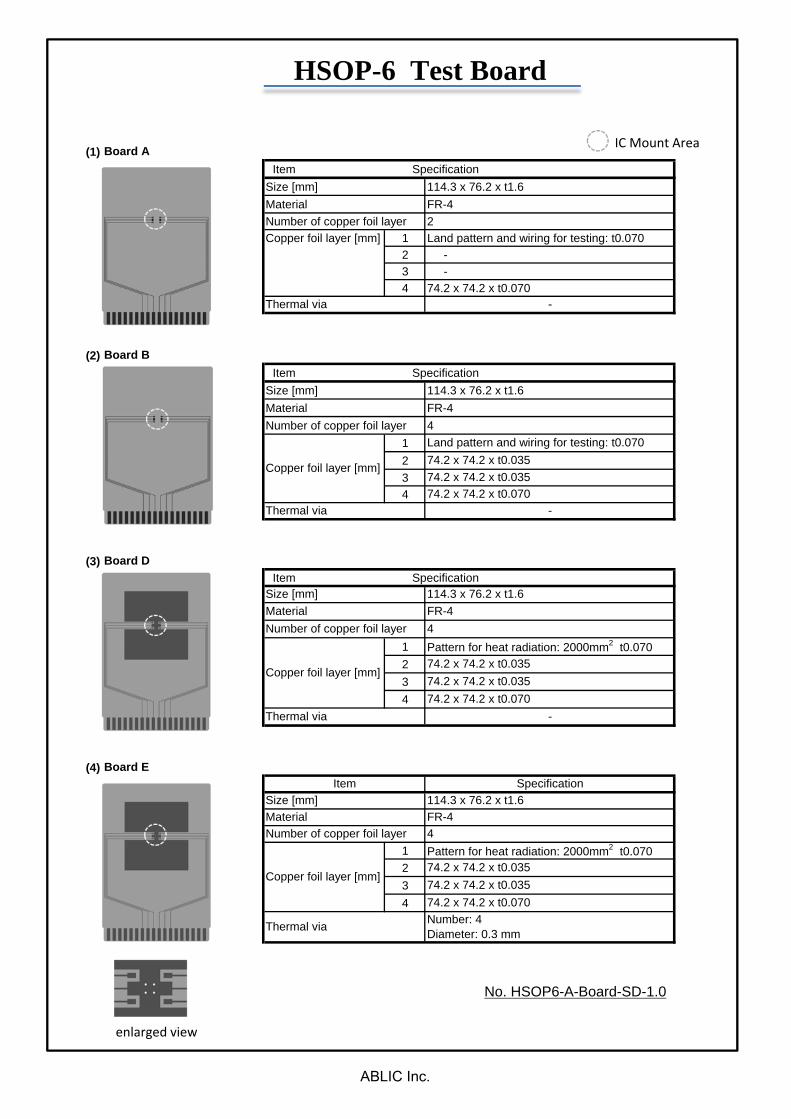
HSOP-6 Test Board
No. HSOP6-A-Board-SD-1.0
ABLIC Inc.
(1)Item Specification
Size [mm] 114.3 x 76.2 x t1.6
Material FR-4Number of copper foil layer 2Copper foil layer [mm] 1 Land pattern and wiring for testing: t0.070
2 -3 -4 74.2 x 74.2 x t0.070
(2)Item Specification
Size [mm] 114.3 x 76.2 x t1.6
Material FR-4Number of copper foil layer 4Copper foil layer [mm] 1 Land pattern and wiring for testing: t0.070
2 74.2 x 74.2 x t0.0353 74.2 x 74.2 x t0.0354 74.2 x 74.2 x t0.070
(3)Item Specification
Size [mm] 114.3 x 76.2 x t1.6
Material FR-4
Number of copper foil layer 4Copper foil layer [mm] 1 Pattern for heat radiation: 2000mm2 t0.070
2 74.2 x 74.2 x t0.0353 74.2 x 74.2 x t0.0354 74.2 x 74.2 x t0.070
(4)Item Specification
Size [mm] 114.3 x 76.2 x t1.6
Material FR-4
Number of copper foil layer 4Copper foil layer [mm] 1 Pattern for heat radiation: 2000mm2 t0.070
2 74.2 x 74.2 x t0.0353 74.2 x 74.2 x t0.0354 74.2 x 74.2 x t0.070
Board E
Thermal via Number: 4Diameter: 0.3 mm
Board D
Thermal via -
Board B
Thermal via -
Thermal via -
Board AIC Mount Area
enlarged view
SOT-89-5 Test Board
No. SOT895-A-Board-SD-1.0
ABLIC Inc.
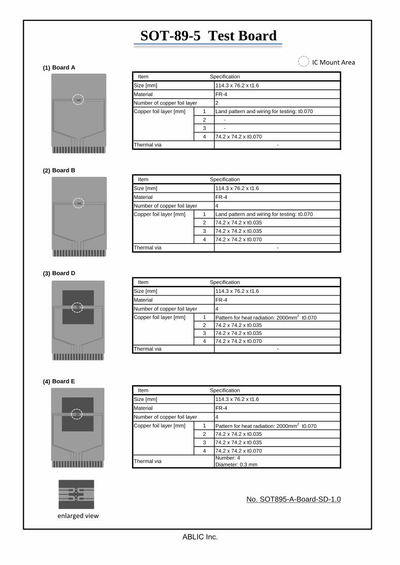
(1)
1234
(2)
1234
(3)
1234
Board A
Item SpecificationSize [mm] 114.3 x 76.2 x t1.6Material FR-4Number of copper foil layer 2
Copper foil layer [mm]
Land pattern and wiring for testing: t0.070--
74.2 x 74.2 x t0.070Thermal via -
Board B
Item SpecificationSize [mm] 114.3 x 76.2 x t1.6Material FR-4Number of copper foil layer 4
Copper foil layer [mm]
Land pattern and wiring for testing: t0.07074.2 x 74.2 x t0.03574.2 x 74.2 x t0.03574.2 x 74.2 x t0.070
Thermal via -
Board C
Item SpecificationSize [mm] 114.3 x 76.2 x t1.6Material FR-4Number of copper foil layer 4
Copper foil layer [mm]
Land pattern and wiring for testing: t0.07074.2 x 74.2 x t0.03574.2 x 74.2 x t0.03574.2 x 74.2 x t0.070
Thermal via Number: 4Diameter: 0.3 mm
IC Mount Area
enlarged view
HTMSOP-8 Test Board
No. HTMSOP8-A-Board-SD-1.0
ABLIC Inc.
(4)
1234
(5)
1234
Board D
Item SpecificationSize [mm] 114.3 x 76.2 x t1.6Material FR-4Number of copper foil layer 4
Copper foil layer [mm]
Pattern for heat radiation: 2000mm2 t0.07074.2 x 74.2 x t0.03574.2 x 74.2 x t0.03574.2 x 74.2 x t0.070
74.2 x 74.2 x t0.03574.2 x 74.2 x t0.035
Thermal via -
Board E
Item SpecificationSize [mm] 114.3 x 76.2 x t1.6
74.2 x 74.2 x t0.070
Thermal via Number: 4Diameter: 0.3 mm
Material FR-4Number of copper foil layer 4
Copper foil layer [mm]
Pattern for heat radiation: 2000mm2 t0.070
IC Mount Area
enlarged view
HTMSOP-8 Test Board
No. HTMSOP8-A-Board-SD-1.0
enlarged view
ABLIC Inc.
(1)
1234
(2)
1234
Thermal via -
Material FR-4Number of copper foil layer 4
Copper foil layer [mm]
Land pattern and wiring for testing: t0.07074.2 x 74.2 x t0.03574.2 x 74.2 x t0.03574.2 x 74.2 x t0.070
Thermal via -
Board B
Item SpecificationSize [mm] 114.3 x 76.2 x t1.6
Number of copper foil layer 2
Copper foil layer [mm]
Land pattern and wiring for testing: t0.070--
74.2 x 74.2 x t0.070
Board A
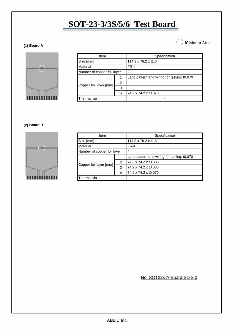
Item SpecificationSize [mm] 114.3 x 76.2 x t1.6Material FR-4
IC Mount Area
SOT-23-3/3S/5/6 Test Board
No. SOT23x-A-Board-SD-2.0
ABLIC Inc.
���
�����
���
����
������ ��
� ����������
�������������������������
���� ��
���
����
��� �!
!��"
����� ����������
��
!��� �!
���� � �
��
���
�����
���
����
������ ��
��
� !
#!�"� �!
#!�� ��� � �
!��� �!�� � �!
��$� �!
�� � � �
%��&�&�'�()���
*� � �!�! �+�)(,��-* � � ��
�����������./'' ��' � �/+�
����� ���.����!�
� ���.����!�
0 �!� �
���
�����
���
����
������ ��
� 1
�� ��
#!2� ��#�!� ��
��3/'4�&�&'/5��4����),��(��)'/3�+/')
!2�*�!�
!"�*�!�
�����������6��3
����� ���6����!�
� ���6����!�
��
7�8� *9
���
�����
���
����
������ ��
��
��
���*
������������/�&�6�(�����&/)���
� ��������!�
����� ��������!�
!��"
��
������ ��
���
�����
���
����
���� ��������������
��
���������������������
��������������
�������� ��!
��������
�
� � �
� �
"��
���������
������ ��
���
�����
���
����
��
�
�
�
#��������
# �� ��"�����
�� ��� ������
$�!���
��������
��%�%�&�'(���
������ ) ��*�('+��,��������-
�������./&& ��& � �/*�
���� ������.���� ��
������.���� ��
0�� ����
������ ��
���
�����
���
����
��
1�2� �3���
�������4��5
���� ������4���� ��
������4���� ��
�����
# "����#� ����
��5/&6�%�%&/7��6����(+��'��(&/5�*/&(
!��� ��
"��� ��
������ ��
���
�����
���
����
��
��������������/�%�4�'�����%/(���
����������� ��
��!
��!$
��! ��!
"��
���� ����������� ��
���
�����
���
����
������ ��
���� ��������������
��
��������������������
��������������
�������
��!�
�������
� "
� �
��!�
���#����
���������
���
�����
���
����
������ ��
��
�
��
"
$�������
$�� ���� ��"����
�������%������
��#����
�������
��&�&�'�()���
�������*���+�)(,��-��������.
�������/0'' ��' � �0+�
������/�������
���� ������/�������
���
�����
���
����
������ ��
��
1�2� �3���
����
�"� ���
��4
����
$�"����$�����%
��50'6�&�&'07��6����),��(��)'05�+0')
�������8��5
���� ������8�������
������8�������
���
�����
���
����
������ ��
��
��������������0�&�8�(�����&0)���
���� ��������������
��������������
��#�
��!� ��!�
���"
���
�����
���
����
������ ��
�� ���� �� ����
�������
�� ����
� ��
�� ����
�������
�������
��� ����
�������
�
����� ���������� !�� !
������� ����������
��� ����������
� "
���
��
���
�����
���
����
������ ��
�������
������� �������#�� $������
������� #�� $���
���
��% ����
�� �
�
������� ��&�������
��� ��&�������
����� ��&'(( �� ( � �')�
*��+�+�(�,-��
�������.���)�-,/�!�0���������1
��
���
�����
���
����
������ ��
��� �'2�
��������
3�4� �5���
.��"1.��"1
������� ��6�������
��� ��6�������
����� ��6��7
� 7'(8�+�+('9� 8�� �-/��,� -('7�)'(-
��
���
�����
���
����
������ ��
�� �����
� �
�������
��������
��������� �
����
��������������� !"#��"#
����$��������������
$��������������
���
�����
���
����
������ ��
���������
��������
���������
���
���������
��������
���������
��������
��
� �
���������%&''�!'��&(!
$!!)�)�'!*+��"
����$������%�������
$������%�������
,������
���
�����
���
����
������ ��
���� &-�
��������
.�/� �0���
1��231��23
������
�"4&'5!)�)'&6�"5��"�+7!�*!"+'&4�(&'+
���������8!!4
����$������8�������
$������8�������
���
�����
���
����
������ ��
����
���� ���� ����
���������������&")�8!*� !")&+��"
����$��������������
$��������������
�� �
���
�����
���
����
������ ��
�� ����
�� ����
�� �����
�������
���������������� � �
��
�������������������
���������������
��������������� !"��!"
��
���
�����
���
����
������ ��
#���������
��������
#��������� ������� �������
��������
�������
���
� �
�����������$�������
�������$�������
��������$%&& � & � �%'
( )�)�& *+��!
�������,���'�+*- ".��������/
��
���
�����
���
����
������ ��
�����%0�
������
#������
,��1/ ,��1/
2�3� �4���
�����������5�������
�������5�������
��������5 6
�!6%&7 )�)&%8�!7��!�+- �* !+&%6�'%&+
��
Disclaimers (Handling Precautions) 1. All the information described herein (product data, specifications, figures, tables, programs, algorithms and application
circuit examples, etc.) is current as of publishing date of this document and is subject to change without notice.
2. The circuit examples and the usages described herein are for reference only, and do not guarantee the success of any specific mass-production design. ABLIC Inc. is not responsible for damages caused by the reasons other than the products described herein (hereinafter "the products") or infringement of third-party intellectual property right and any other right due to the use of the information described herein.
3. ABLIC Inc. is not responsible for damages caused by the incorrect information described herein.
4. Be careful to use the products within their specified ranges. Pay special attention to the absolute maximum ratings, operation voltage range and electrical characteristics, etc. ABLIC Inc. is not responsible for damages caused by failures and / or accidents, etc. that occur due to the use of the products outside their specified ranges.
5. When using the products, confirm their applications, and the laws and regulations of the region or country where they are used and verify suitability, safety and other factors for the intended use.
6. When exporting the products, comply with the Foreign Exchange and Foreign Trade Act and all other export-related laws, and follow the required procedures.
7. The products must not be used or provided (exported) for the purposes of the development of weapons of mass destruction or military use. ABLIC Inc. is not responsible for any provision (export) to those whose purpose is to develop, manufacture, use or store nuclear, biological or chemical weapons, missiles, or other military use.
8. The products are not designed to be used as part of any device or equipment that may affect the human body, human life, or assets (such as medical equipment, disaster prevention systems, security systems, combustion control systems, infrastructure control systems, vehicle equipment, traffic systems, in-vehicle equipment, aviation equipment, aerospace equipment, and nuclear-related equipment), excluding when specified for in-vehicle use or other uses. Do not apply the products to the above listed devices and equipments without prior written permission by ABLIC Inc. Especially, the products cannot be used for life support devices, devices implanted in the human body and devices that directly affect human life, etc. Prior consultation with our sales office is required when considering the above uses. ABLIC Inc. is not responsible for damages caused by unauthorized or unspecified use of our products.
9. Semiconductor products may fail or malfunction with some probability. The user of the products should therefore take responsibility to give thorough consideration to safety design including redundancy, fire spread prevention measures, and malfunction prevention to prevent accidents causing injury or death, fires and social damage, etc. that may ensue from the products' failure or malfunction. The entire system must be sufficiently evaluated and applied on customer's own responsibility.
10. The products are not designed to be radiation-proof. The necessary radiation measures should be taken in the product design by the customer depending on the intended use.
11. The products do not affect human health under normal use. However, they contain chemical substances and heavy metals and should therefore not be put in the mouth. The fracture surfaces of wafers and chips may be sharp. Be careful when handling these with the bare hands to prevent injuries, etc.
12. When disposing of the products, comply with the laws and ordinances of the country or region where they are used.
13. The information described herein contains copyright information and know-how of ABLIC Inc. The information described herein does not convey any license under any intellectual property rights or any other rights belonging to ABLIC Inc. or a third party. Reproduction or copying of the information from this document or any part of this document described herein for the purpose of disclosing it to a third-party without the express permission of ABLIC Inc. is strictly prohibited.
14. For more details on the information described herein, contact our sales office.
2.0-2018.01
www.ablicinc.com