Embed Size (px)
Citation preview

SAM3X-EK....................................................................................................................
User Guide
11156A–ATARM–25-May-12
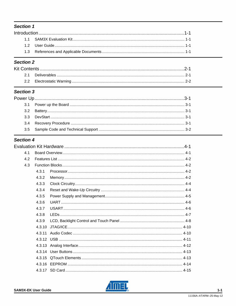
Section 1Introduction.................................................................................................................1-1
1.1 SAM3X Evaluation Kit ........................................................................................................ 1-1
1.2 User Guide ......................................................................................................................... 1-1
1.3 References and Applicable Documents ............................................................................. 1-1
Section 2Kit Contents ................................................................................................................2-1
2.1 Deliverables ....................................................................................................................... 2-1
2.2 Electrostatic Warning ......................................................................................................... 2-2
Section 3Power Up....................................................................................................................3-1
3.1 Power up the Board ........................................................................................................... 3-1
3.2 Battery................................................................................................................................ 3-1
3.3 DevStart ............................................................................................................................. 3-1
3.4 Recovery Procedure .......................................................................................................... 3-1
3.5 Sample Code and Technical Support ................................................................................ 3-2
Section 4Evaluation Kit Hardware .............................................................................................4-1
4.1 Board Overview.................................................................................................................. 4-1
4.2 Features List ...................................................................................................................... 4-2
4.3 Function Blocks.................................................................................................................. 4-2
4.3.1 Processor............................................................................................................. 4-2
4.3.2 Memory................................................................................................................ 4-2
4.3.3 Clock Circuitry...................................................................................................... 4-4
4.3.4 Reset and Wake-Up Circuitry .............................................................................. 4-4
4.3.5 Power Supply and Management.......................................................................... 4-5
4.3.6 UART ................................................................................................................... 4-6
4.3.7 USART................................................................................................................. 4-6
4.3.8 LEDs .................................................................................................................... 4-7
4.3.9 LCD, Backlight Control and Touch Panel ............................................................ 4-8
4.3.10 JTAG/ICE........................................................................................................... 4-10
4.3.11 Audio Codec ...................................................................................................... 4-10
4.3.12 USB ................................................................................................................... 4-11
4.3.13 Analog Interface................................................................................................. 4-12
4.3.14 User Buttons ...................................................................................................... 4-13
4.3.15 QTouch Elements .............................................................................................. 4-13
4.3.16 EEPROM ........................................................................................................... 4-14
4.3.17 SD Card ............................................................................................................. 4-15
SAM3X-EK User Guide 1-1
11156A–ATARM–25-May-12
4.3.18 ZigBee ............................................................................................................... 4-15
4.3.19 PIO Expansion................................................................................................... 4-17
4.3.20 Ethernet MAC 10/100 (EMAC) .......................................................................... 4-18
4.3.21 CAN ................................................................................................................... 4-18
4.4 Configuration.................................................................................................................... 4-19
4.4.1 PIO Usage ......................................................................................................... 4-20
4.4.2 Jumpers ............................................................................................................. 4-25
4.4.3 Test Points......................................................................................................... 4-26
4.4.4 Assigned PIO Lines, Disconnection Possibility.................................................. 4-26
Section 5Schematics .................................................................................................................5-1
5.1 Schematics......................................................................................................................... 5-1
Section 6Troubleshooting..........................................................................................................6-1
6.1 Self-Test............................................................................................................................. 6-1
6.2 Board Recovery ................................................................................................................. 6-1
Section 7Revision History..........................................................................................................7-1
7.1 Revision History ................................................................................................................. 7-1
1-2 SAM3X-EK User Guide
11156A–ATARM–25-May-12
Section 1
Introduction
1.1 SAM3X Evaluation Kit
The SAM3X Evaluation Kit (SAM3X-EK) allows to evaluate the SAM3X series devices. It has enough features to demonstrate most of the product’s capabilities to its users. The SAM3X-EK also features extension connectors to allow users to add new interfaces in case they are not on-board.
1.2 User Guide
This guide gives details on how the SAM3X-EK has been designed. It is made up of 6 sections:
Section 1 includes references, applicable documents
Section 2 describes the kit contents and main features
Section 3 provides instructions on how to power up the SAM3X-EK and describes how to use it
Section 4 describes the hardware resources, including default jumper and switch settings, and the schematics
Section 5 provides all the board schematics
Section 6 gives troubleshooting recommendations
1.3 References and Applicable Documents
Table 1-1. References and Applicable Documents
Title Comment
SAM3X Datasheet http://www.atmel.com/dyn/products/devices.asp?category_id=163&family_id=605&subfamily_id=2363
SAM3X-EK User Guide 1-1
11156A–ATARM–25-May-12
Section 2
Kit Contents
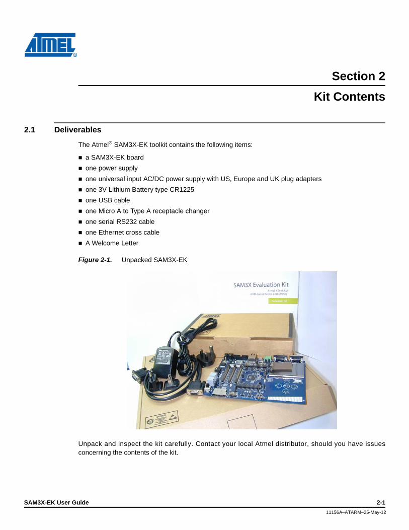
2.1 Deliverables
The Atmel® SAM3X-EK toolkit contains the following items:
a SAM3X-EK board
one power supply
one universal input AC/DC power supply with US, Europe and UK plug adapters
one 3V Lithium Battery type CR1225
one USB cable
one Micro A to Type A receptacle changer
one serial RS232 cable
one Ethernet cross cable
A Welcome Letter
Figure 2-1. Unpacked SAM3X-EK
Unpack and inspect the kit carefully. Contact your local Atmel distributor, should you have issues concerning the contents of the kit.
SAM3X-EK User Guide 2-1
11156A–ATARM–25-May-12
2.2 Electrostatic Warning
The SAM3X-EK board is shipped in a protective anti-static bag. The board must not be subjected to high electrostatic potentials. A grounding strap or similar protective device should be worn when handling the board. Avoid touching the components or any other metallic element of the board.
2-2 SAM3X-EK User Guide
11156A–ATARM–25-May-12
Section 3
Power Up
3.1 Power up the Board
Unpack the board taking care to avoid electrostatic discharge. Unpack the power supply, select the right power plug adapter corresponding to that of your country, and insert it in the power supply.
Connect the power supply DC connector to the board and plug the power supply to an AC power plug.
The board LCD should light up and display a welcome page. Then, click or touch icons displayed on the screen and enjoy the demo.
3.2 Battery
The SAM3X-EK ships with a 3V coin battery.
This battery is not required for the board to start up.
The coin battery is provided for user convenience in case the user would like to exercise the date and time backup function of the SAM3X series devices when the board is switched off.
3.3 DevStart
The on-board NAND Flash contains “SAM3X-EK DevStart”.
It is stored in the “SAM3X-EK DevStart” folder on the USB Flash disk available when the SAM3X-EK is connected to a host computer and you click on the Flash Disk icon of the on-board demo.
Click the file “welcome.html” in this folder to launch SAM3X-EK DevStart.
SAM3X-EK DevStart guides you through installation processes of IAR™ EWARM, Keil MDK and GNU toolkits. Then, it gives you step-by-step instructions on how to rebuild a single example project and how to program it into the SAM3X-EK. Optionally, if you have a SAM-ICE™, instructions are also given about how to debug the code.
We recommend that you backup the “SAM3X-EK DevStart” folder on your computer before launching it.
3.4 Recovery Procedure
The DevStart ends by giving step-by-step instructions on how to recover the SAM3X-EK to the state as it was when shipped by Atmel.
Follow the instructions if you deleted the contents of the embedded Flash or the NAND Flash and want to recover from this situation.
SAM3X-EK User Guide 3-1
11156A–ATARM–25-May-12
3.5 Sample Code and Technical Support
After boot up, you can run some sample code or your own application on the development kit. You can download sample code and get technical support from Atmel website: www.atmel.com
3-2 SAM3X-EK User Guide
11156A–ATARM–25-May-12
Section 4
Evaluation Kit Hardware
4.1 Board Overview
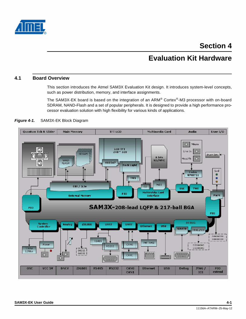
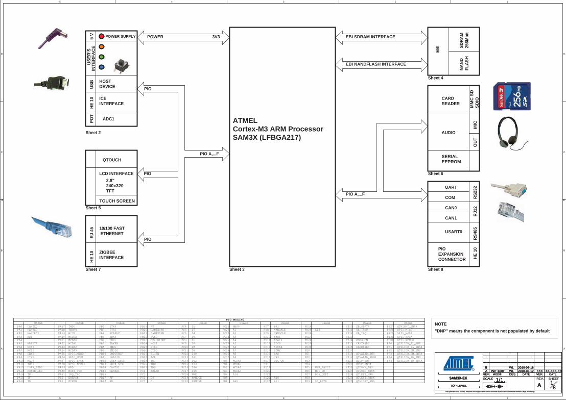
This section introduces the Atmel SAM3X Evaluation Kit design. It introduces system-level concepts, such as power distribution, memory, and interface assignments.
The SAM3X-EK board is based on the integration of an ARM® Cortex®-M3 processor with on-board SDRAM, NAND-Flash and a set of popular peripherals. It is designed to provide a high performance pro-cessor evaluation solution with high flexibility for various kinds of applications.
Figure 4-1. SAM3X-EK Block Diagram
SAM3X-EK User Guide 4-1
11156A–ATARM–25-May-12
4.2 Features List
Here is the list of the main board components and interfaces:
SAM3X8H LFBGA chip with optional socket footprint
12 MHz crystal
32.768 KHz crystal
SDRAM
NAND-Flash
Backup Battery
2.8 inch TFT color LCD display with touch-panel and backlight
UART port with level shifter IC
USART port with level shifter IC
Audio codec with input and output jacks: stereo headphone out and mono microphone in
SD/MMC interface
QTouch elements: Up, Down, Left, Right, Valid and Slider
Reset and Wake-Up buttons: NRST, NRSTB, FWUP
User buttons: Left and Right
High Speed USB Host/Device port
JTAG/ICE port
On-board power regulation with shutdown control (by the SAM3 chip)
Three user LEDs
Power LED
User potentiometer connected to the ADC input
IEEE 802.15.4 / ZigBee® connector
Two serial CAN 2.0B communication port via two RJ12 connectors
One Ethernet Physical Transceiver Layer with RJ45 connector
Five peripheral Input/Output Extension Connectors HE10 (PIOA, B, C, D, E)
4.3 Function Blocks
4.3.1 Processor
The SAM3X-EK is equipped with a SAM3X8H in a LFBGA217 package.
4.3.2 Memory
The SAM3X8H chip embeds:
512 Kbytes of embedded Flash
100Kbytes of embedded SRAM with dual bank
16 Kbytes of ROM with embedded bootloader routines (UART, USB) and IAP (In-Application Programming functions) routines.
4-2 SAM3X-EK User Guide
11156A–ATARM–25-May-12
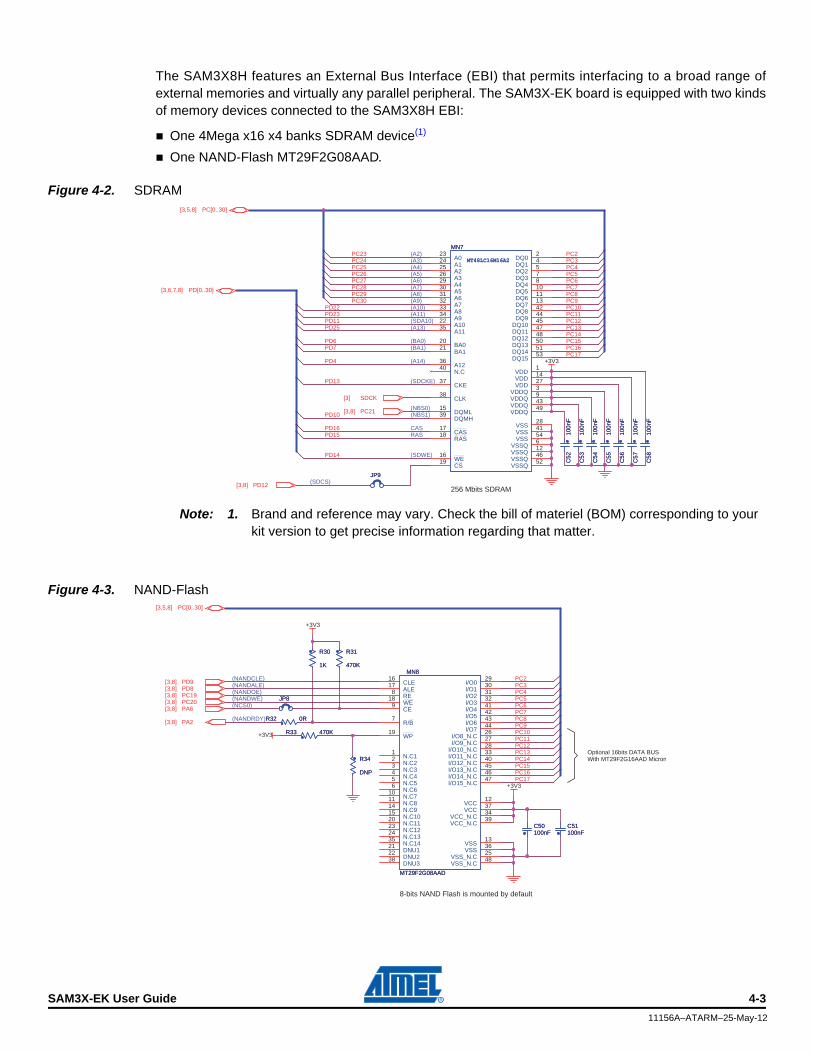
The SAM3X8H features an External Bus Interface (EBI) that permits interfacing to a broad range of external memories and virtually any parallel peripheral. The SAM3X-EK board is equipped with two kinds of memory devices connected to the SAM3X8H EBI:
One 4Mega x16 x4 banks SDRAM device(1)
One NAND-Flash MT29F2G08AAD.
Figure 4-2. SDRAM
Note: 1. Brand and reference may vary. Check the bill of materiel (BOM) corresponding to your kit version to get precise information regarding that matter.
Figure 4-3. NAND-Flash
256 Mbits SDRAM
(SDA10)
(A2)(A3)(A4)(A5)(A6)(A7)(A8)(A9)(A10)(A11)
(A13)
(A14)
(BA0)(BA1)
(SDCKE)
(NBS0)(NBS1)
CASRAS
(SDWE)
(SDCS)
PD6PD7
PD4
PC2PC3PC4PC5PC6PC7
PD16
PC8
PD13
PD10
PD15
PC9
PD14
PC10PD22PD23
PC29
PC27
PC30
PC26
PC28
PC11PC12PC13PC14PC15
PD25
PC16PC17
PD11
PC23PC24PC25
+3V3
SDCK[3]
PC21[3,8]
PC[0..30][3,5,8]
PD[0..30][3,6,7,8]
PD12[3,8]
C58
100n
FC
5810
0nF
C52
100n
FC
5210
0nF
C57
100n
FC
5710
0nF
C55
100n
FC
5510
0nF
MT48LC16M16A2
MN7
MT48LC16M16A2
MN7
A023
A124
A225
A326
A429
A530
A631
A732
A833
A934
A1022
BA020
A1236
DQ02
DQ14
DQ25
DQ37
DQ48
DQ510
DQ611
DQ713
DQ842
DQ944
DQ1045
DQ1147
DQ1248
DQ1350
DQ1451
DQ1553
VDD1
VSS28
VSS41
VDDQ3VDD27
N.C40
CLK38
CKE37
DQML15
DQMH39
CAS17
RAS18
WE16
CS19
VDDQ9
VDDQ43
VDDQ49
VSSQ6
VSSQ12
VSSQ46
VSSQ52
VDD14
VSS54
A1135
BA121
C56
100n
FC
5610
0nF
C54
100n
FC
5410
0nF
C53
100n
FC
5310
0nF
JP9JP9
(NCS0)
(NANDRDY)
(NANDALE)(NANDCLE)
Optional 16bits DATA BUSWith MT29F2G16AAD Micron
(NANDWE)(NANDOE)
8-bits NAND Flash is mounted by default
PC8
PC2
PC5PC6
PC4PC3
PC7
PC9
PC16
PC10
PC13PC14
PC12PC11
PC15
PC17
+3V3
+3V3
+3V3
PC[0..30][3,5,8]
PD9[3,8]PD8[3,8]PC19[3,8]PC20[3,8]PA6[3,8]
PA2[3,8]
R31
470K
R31
470K
C51100nFC51100nF
R33 470KR33 470K
R34
DNP
R34
DNP
C50100nFC50100nF
R32 0RR32 0R
JP8JP8
MN8
MT29F2G08AAD
MN8
MT29F2G08AAD
WE18
N.C66
VCC37
CE9
RE8
N.C1120
WP19
N.C55
N.C11
N.C22
N.C33
N.C44
DNU121
DNU222
N.C1223
N.C1324
R/B7
I/O8_N.C26
I/O9_N.C27
I/O10_N.C28
I/O029
VCC_N.C34
N.C1435
VSS36
DNU338
VCC_N.C39
VCC12
VSS13
ALE17
N.C811 N.C710
N.C914
N.C1015
CLE16
VSS_N.C25
I/O11_N.C33
I/O130
I/O332I/O231
I/O15_N.C47I/O14_N.C46I/O13_N.C45
I/O744I/O643I/O542I/O441
I/O12_N.C40
VSS_N.C48
R30
1K
R30
1K
SAM3X-EK User Guide 4-3
11156A–ATARM–25-May-12
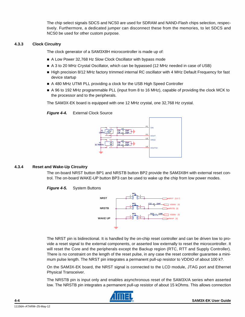
The chip select signals SDCS and NCS0 are used for SDRAM and NAND-Flash chips selection, respec-tively. Furthermore, a dedicated jumper can disconnect these from the memories, to let SDCS and NCS0 be used for other custom purpose.
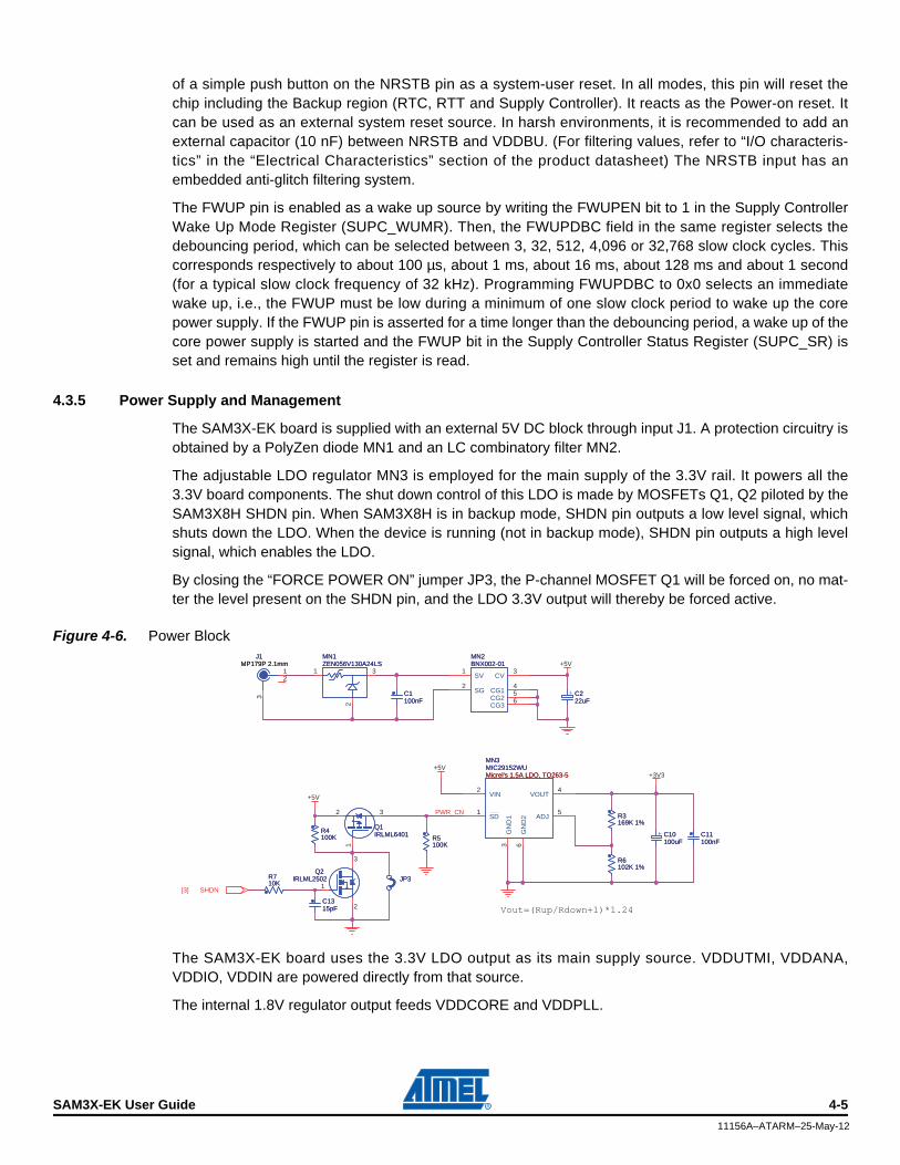
4.3.3 Clock Circuitry
The clock generator of a SAM3X8H microcontroller is made up of:
A Low Power 32,768 Hz Slow Clock Oscillator with bypass mode
A 3 to 20 MHz Crystal Oscillator, which can be bypassed (12 MHz needed in case of USB)
High precision 8/12 MHz factory trimmed internal RC oscillator with 4 MHz Default Frequency for fast device startup
A 480 MHz UTMI PLL providing a clock for the USB High Speed Controller
A 96 to 192 MHz programmable PLL (input from 8 to 16 MHz), capable of providing the clock MCK to the processor and to the peripherals.
The SAM3X-EK board is equipped with one 12 MHz crystal, one 32,768 Hz crystal.
Figure 4-4. External Clock Source
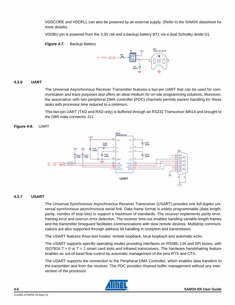
4.3.4 Reset and Wake-Up Circuitry
The on-board NRST button BP1 and NRSTB button BP2 provide the SAM3X8H with external reset con-trol. The on-board WAKE-UP button BP3 can be used to wake up the chip from low power modes.
Figure 4-5. System Buttons
The NRST pin is bidirectional. It is handled by the on-chip reset controller and can be driven low to pro-vide a reset signal to the external components, or asserted low externally to reset the microcontroller. It will reset the Core and the peripherals except the Backup region (RTC, RTT and Supply Controller). There is no constraint on the length of the reset pulse, in any case the reset controller guarantee a mini-mum pulse length. The NRST pin integrates a permanent pull-up resistor to VDDIO of about 100 k?.
On the SAM3X-EK board, the NRST signal is connected to the LCD module, JTAG port and Ethernet Physical Transceiver.
The NRSTB pin is input only and enables asynchronous reset of the SAM3X/A series when asserted low. The NRSTB pin integrates a permanent pull-up resistor of about 15 kOhms. This allows connection
XOUTP2
XINP1
XIN32U5
XOUT32U6
C33 10pFC33 10pF
C40 20pFC40 20pF
C36 10pFC36 10pF
Y232.768KHz
Y232.768KHz
123 4
Y112MHz
Y112MHz
123 4
C42 20pFC42 20pF
NRST
NRSTB
WAKE UP
NRST [3,5,7]
NRSTB [3]
FWUP [3]
VDDBU [3]
VDDBU [3]BP2BP21
423
BP3BP31
423
C22 10nFC22 10nF
R23 100KR23 100K
BP1BP11
423
4-4 SAM3X-EK User Guide
11156A–ATARM–25-May-12
of a simple push button on the NRSTB pin as a system-user reset. In all modes, this pin will reset the chip including the Backup region (RTC, RTT and Supply Controller). It reacts as the Power-on reset. It can be used as an external system reset source. In harsh environments, it is recommended to add an external capacitor (10 nF) between NRSTB and VDDBU. (For filtering values, refer to “I/O characteris-tics” in the “Electrical Characteristics” section of the product datasheet) The NRSTB input has an embedded anti-glitch filtering system.
The FWUP pin is enabled as a wake up source by writing the FWUPEN bit to 1 in the Supply Controller Wake Up Mode Register (SUPC_WUMR). Then, the FWUPDBC field in the same register selects the debouncing period, which can be selected between 3, 32, 512, 4,096 or 32,768 slow clock cycles. This corresponds respectively to about 100 µs, about 1 ms, about 16 ms, about 128 ms and about 1 second (for a typical slow clock frequency of 32 kHz). Programming FWUPDBC to 0x0 selects an immediate wake up, i.e., the FWUP must be low during a minimum of one slow clock period to wake up the core power supply. If the FWUP pin is asserted for a time longer than the debouncing period, a wake up of the core power supply is started and the FWUP bit in the Supply Controller Status Register (SUPC_SR) is set and remains high until the register is read.
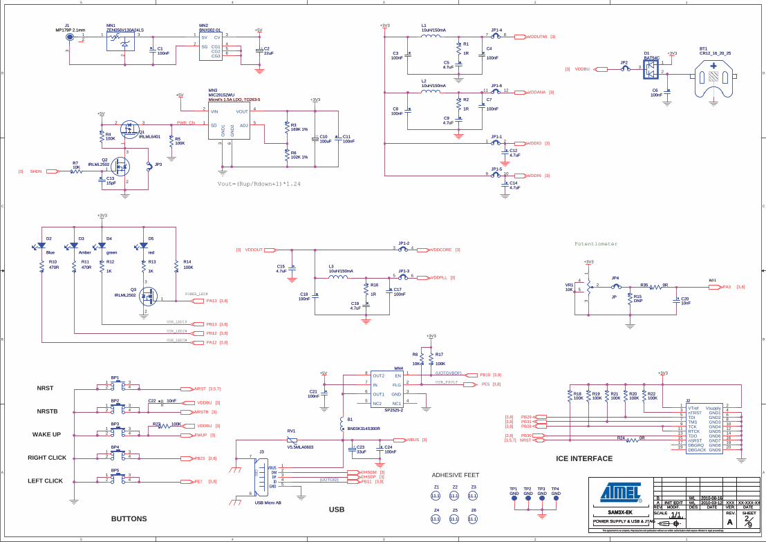
4.3.5 Power Supply and Management
The SAM3X-EK board is supplied with an external 5V DC block through input J1. A protection circuitry is obtained by a PolyZen diode MN1 and an LC combinatory filter MN2.
The adjustable LDO regulator MN3 is employed for the main supply of the 3.3V rail. It powers all the 3.3V board components. The shut down control of this LDO is made by MOSFETs Q1, Q2 piloted by the SAM3X8H SHDN pin. When SAM3X8H is in backup mode, SHDN pin outputs a low level signal, which shuts down the LDO. When the device is running (not in backup mode), SHDN pin outputs a high level signal, which enables the LDO.
By closing the “FORCE POWER ON” jumper JP3, the P-channel MOSFET Q1 will be forced on, no mat-ter the level present on the SHDN pin, and the LDO 3.3V output will thereby be forced active.
Figure 4-6. Power Block
The SAM3X-EK board uses the 3.3V LDO output as its main supply source. VDDUTMI, VDDANA, VDDIO, VDDIN are powered directly from that source.
The internal 1.8V regulator output feeds VDDCORE and VDDPLL.
Vout=(Rup/Rdown+1)*1.24
PWR_CN
+5V
+5V
+5V+3V3
SHDN[3]
R5100KR5100K
+ C10100uF
+ C10100uF
JP3JP3Q2
IRLML2502Q2
IRLML25021
3
2
J1MP179P 2.1mm
J1MP179P 2.1mm
12
3
MN1ZEN056V130A24LSMN1ZEN056V130A24LS
1
2
3
C1100nFC1100nF
MN2BNX002-01MN2BNX002-01
SV1
SG2
CV3
CG14
CG25
CG36
R3169K 1%R3169K 1%
C11100nFC11100nF
R6102K 1%R6102K 1%
Q1IRLML6401Q1IRLML6401
1
32
+ C222uF
+ C222uF
C1315pFC1315pF
MN3MIC29152WUMicrel's 1.5A LDO, TO263-5
MN3MIC29152WUMicrel's 1.5A LDO, TO263-5
VIN2
VOUT4
SD1
GN
D1
3
ADJ5
GN
D2
6
R710KR710K
R4100KR4100K
SAM3X-EK User Guide 4-5
11156A–ATARM–25-May-12
VDDCORE and VDDPLL can also be powered by an external supply. (Refer to the SAM3X datasheet for more details).
VDDBU pin is powered from the 3.3V rail and a backup battery BT1 via a dual Schottky diode D1.
Figure 4-7. Backup Battery
4.3.6 UART
The Universal Asynchronous Receiver Transmitter features a two-pin UART that can be used for com-munication and trace purposes and offers an ideal medium for on-site programming solutions. Moreover, the association with two peripheral DMA controller (PDC) channels permits packet handling for these tasks with processor time reduced to a minimum.
This two-pin UART (TXD and RXD only) is buffered through an RS232 Transceiver MN14 and brought to the DB9 male connector J11.
Figure 4-8. UART
4.3.7 USART
The Universal Synchronous Asynchronous Receiver Transceiver (USART) provides one full duplex uni-versal synchronous asynchronous serial link. Data frame format is widely programmable (data length, parity, number of stop bits) to support a maximum of standards. The receiver implements parity error, framing error and overrun error detection. The receiver time-out enables handling variable-length frames and the transmitter timeguard facilitates communications with slow remote devices. Multidrop communi-cations are also supported through address bit handling in reception and transmission.
The USART features three test modes: remote loopback, local loopback and automatic echo.
The USART supports specific operating modes providing interfaces on RS485, LIN and SPI buses, with ISO7816 T = 0 or T = 1 smart card slots and infrared transceivers. The hardware handshaking feature enables an out-of-band flow control by automatic management of the pins RTS and CTS.
The USART supports the connection to the Peripheral DMA Controller, which enables data transfers to the transmitter and from the receiver. The PDC provides chained buffer management without any inter-vention of the processor.
+3V3
VDDBU[3]JP2JP2
D1BAT54CD1BAT54C
32
1
C6100nFC6
100nF
BT1CR12_16_20_25BT1CR12_16_20_25
UART
(UTXD)(URXD)
+3V3
+3V3 +3V3
PA9[3]PA8[3]
R111100KR111100K
C124100nFC124100nF
C120100nFC120100nF
R112100KR112100K
C121100nFC121100nF
MN14MAX3232CSEMN14MAX3232CSE
T1IN11
T2IN10 R1OUT12
R2OUT9
T1OUT14
T2OUT7R1IN13
R2IN8
V+2
C1+1
C1-3
C2+4
C2-5
V-6
VCC16
GND15
J11J11
5
4
3
2
1
9
8
7
6
10 11
C123100nFC123100nF
C119100nFC119100nF
4-6 SAM3X-EK User Guide
11156A–ATARM–25-May-12
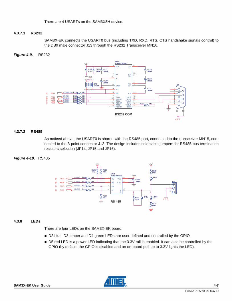
There are 4 USARTs on the SAM3X8H device.
4.3.7.1 RS232
SAM3X-EK connects the USART0 bus (including TXD, RXD, RTS, CTS handshake signals control) to the DB9 male connector J13 through the RS232 Transceiver MN16.
Figure 4-9. RS232
4.3.7.2 RS485
As noticed above, the USART0 is shared with the RS485 port, connected to the transceiver MN15, con-nected to the 3-point connector J12. The design includes selectable jumpers for RS485 bus termination resistors selection (JP14, JP15 and JP16).
Figure 4-10. RS485
4.3.8 LEDs
There are four LEDs on the SAM3X-EK board:
D2 blue, D3 amber and D4 green LEDs are user defined and controlled by the GPIO.
D5 red LED is a power LED indicating that the 3.3V rail is enabled. It can also be controlled by the GPIO (by default, the GPIO is disabled and an on-board pull-up to 3.3V lights the LED).
RS232 COM
(COM0_EN)
(TXD0)(RXD0)(RTS0)(CTS0)
+3V3
+3V3
PA10[3]
PB26[3]
PE14[3]
PA11[3]
PB25[3]
C129100nFC129100nF
C127100nFC127100nF
R123 0RR123 0R
R119 0RR119 0R
C130100nFC130100nF
MN16ADM3312EARUMN16ADM3312EARU
C1+6
C1-20
C2+2
C2-4
C3+24
C3-22
VCC3
V+1
V-21
GND23
SD19
EN5
T1IN7
T1OUT18
R1IN15
R1OUT10
T2IN8
T2OUT17
R2IN14
R2OUT11
T3IN9
T3OUT16
R3IN13
R3OUT12
C128100nFC128100nF
R122 0RR122 0R
C1254.7uFC1254.7uF
C131100nFC131100nF
R124 0RR124 0R
R121 0RR121 0RR120 0RR120 0R
C126100nFC126100nF
J13J13
5
4
3
2
1
9
8
7
6
10 11
RR747KX4RR747KX4
12345 6 7 8
RS 485
(RXD0)
(RTS0)
(CTS0)
(TXD0)
+3V3
+3V3
+3V3
PA10[3]
PB25[3]
PB26[3]
PA11[3]
R113 0RR113 0R
JP14JP14
R10647KR10647K
JP15JP15 JP16JP16R11547KR11547K
MN15ADM3485ARZMN15ADM3485ARZ
RO1
RE2
DE3
DI4
VCC8
GND5
A6
B7
R108DNPR108DNP
R117120RR117120R
R109 0RR109 0R
R110 0RR110 0R
R114 0RR114 0R
R10747KR10747K
C122100nFC122100nF
R118DNPR118DNP
J12J121
2
3
SAM3X-EK User Guide 4-7
11156A–ATARM–25-May-12
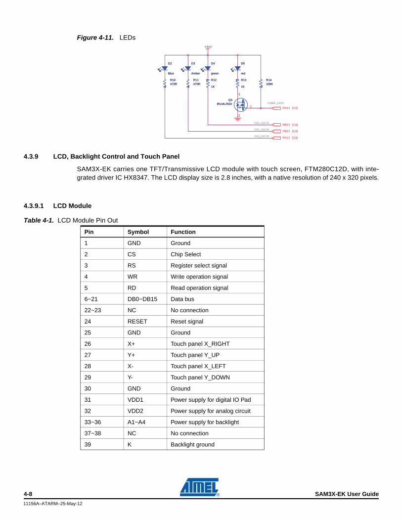
Figure 4-11. LEDs
4.3.9 LCD, Backlight Control and Touch Panel
SAM3X-EK carries one TFT/Transmissive LCD module with touch screen, FTM280C12D, with inte-grated driver IC HX8347. The LCD display size is 2.8 inches, with a native resolution of 240 x 320 pixels.
4.3.9.1 LCD Module
USR_LED1#
USR_LED2#
POWER_LED#
USR_LED3#
+3V3
PA13 [3,8]
PB12 [3,8]
PA12 [3,8]
PB13 [3,8]
R11470RR11470R
R12
1K
R12
1K
R13
1K
R13
1K
Q3IRLML2502
Q3IRLML2502
1
3
2
D4
green
D4
green
R10470RR10470R
D5
red
D5
red
D2
Blue
D2
Blue
R14100KR14100K
D3
Amber
D3
Amber
Table 4-1. LCD Module Pin Out
Pin Symbol Function
1 GND Ground
2 CS Chip Select
3 RS Register select signal
4 WR Write operation signal
5 RD Read operation signal
6~21 DB0~DB15 Data bus
22~23 NC No connection
24 RESET Reset signal
25 GND Ground
26 X+ Touch panel X_RIGHT
27 Y+ Touch panel Y_UP
28 X- Touch panel X_LEFT
29 Y- Touch panel Y_DOWN
30 GND Ground
31 VDD1 Power supply for digital IO Pad
32 VDD2 Power supply for analog circuit
33~36 A1~A4 Power supply for backlight
37~38 NC No connection
39 K Backlight ground
4-8 SAM3X-EK User Guide
11156A–ATARM–25-May-12
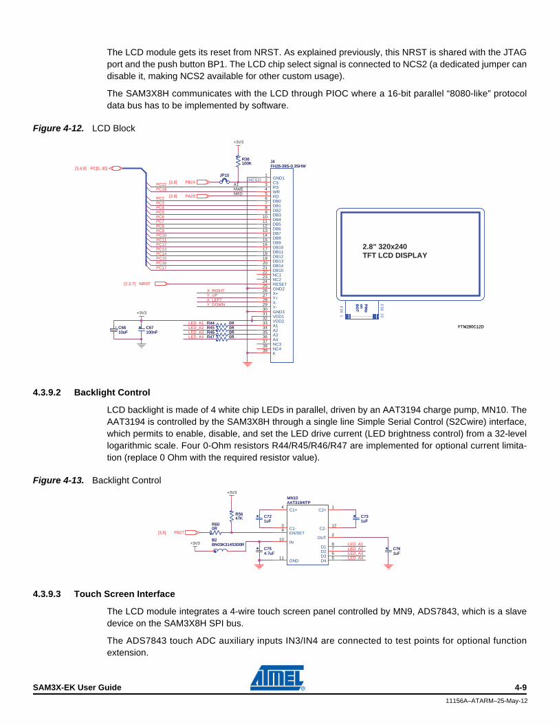
The LCD module gets its reset from NRST. As explained previously, this NRST is shared with the JTAG port and the push button BP1. The LCD chip select signal is connected to NCS2 (a dedicated jumper can disable it, making NCS2 available for other custom usage).
The SAM3X8H communicates with the LCD through PIOC where a 16-bit parallel “8080-like” protocol data bus has to be implemented by software.
Figure 4-12. LCD Block
4.3.9.2 Backlight Control
LCD backlight is made of 4 white chip LEDs in parallel, driven by an AAT3194 charge pump, MN10. The AAT3194 is controlled by the SAM3X8H through a single line Simple Serial Control (S2Cwire) interface, which permits to enable, disable, and set the LED drive current (LED brightness control) from a 32-level logarithmic scale. Four 0-Ohm resistors R44/R45/R46/R47 are implemented for optional current limita-tion (replace 0 Ohm with the required resistor value).
Figure 4-13. Backlight Control
4.3.9.3 Touch Screen Interface
The LCD module integrates a 4-wire touch screen panel controlled by MN9, ADS7843, which is a slave device on the SAM3X8H SPI bus.
The ADS7843 touch ADC auxiliary inputs IN3/IN4 are connected to test points for optional function extension.
(NCS2)A1NWENRD
2.8" 320x240 TFT LCD DISPLAY
PC22PC18
PC3PC2
PC4
PC6PC5
PC8PC9
PC7
PC16
PC10
PC13PC14
PC11
PC15
PC12
PC17
X_RIGHT
X_LEFTY_DOWN
Y_UP
LED_A1LED_A2LED_A3LED_A4
+3V3
+3V3
NRST[2,3,7]
PC[0..30][3,4,8]
PB24[3,8]
PA29[3,8]PIN
sonB
OT
PIN 39
PIN 1
FTM280C12D
PINs
onBO
T
PIN 39
PIN 1
FTM280C12D+ C6610uF
+ C6610uF
J4FH26-39S-0.3SHWJ4FH26-39S-0.3SHW
GND11
CS2
RS3
WR4
RD5
DB06
DB17
DB28
DB39
DB410
DB511
DB612
DB713
DB814
DB915
DB1016
DB1117
DB1218
DB1319
DB1420
DB1521
NC122
NC223
RESET24
GND225
X+26
Y+27
X-28
Y-29
GND330
VDD131
VDD232
A133
A234
A335
A436
NC337
NC438
K39
R36100KR36100K
R44 0RR44 0RR45 0RR45 0RR46 0RR46 0RR47 0RR47 0R
JP10JP10
C67100nFC67100nF
LED_A1LED_A2LED_A3LED_A4
+3V3
+3V3
PB27[3,8]
C731uFC731uF
C761uFC761uF
B2BN03K314S300RB2BN03K314S300R
C754.7uFC754.7uF
R5647KR5647K
R600RR600R
MN10AAT3194ITPMN10AAT3194ITP
C1+4
C1-3
EN/SET9
C2+1
C2-12
OUT2
IN10
GND11
D18
D27
D36
D45
C721uFC721uF
SAM3X-EK User Guide 4-9
11156A–ATARM–25-May-12
Figure 4-14. Touch Screen Controller
4.3.10 JTAG/ICE
A standard 20-pin JTAG connector is implemented on the SAM3X-EK for any ARM JTAG emulator con-nection, such as SAM-ICE from Segger.
Note that the NRST net is connected to the system button BP1, and is also used to reset the LCD mod-ule. 0-Ohm resistor R24 may be removed in order to isolate the JTAG port from the system reset signal.
Figure 4-15. JTAG Connector
4.3.11 Audio Codec
The SAM3X-EK includes a WOLFSON codec WM8731 for digital sound input and output. This interface includes audio jacks for:
microphone input
headphone output
The SAM3X8H programmable clock output is used to generate the WM8731 master clock (MCLK). The SAM3X8H ODT (On-Die Termination) feature guarantees a signal integrity on this clock line without the need for external discrete components.
WM8731 pin 21 MODE is pulled down by default; this configures the device as a TWI device for internal register access.
Pin15 CSB is pulled up, which sets its TWI address as 33 [0x0011011].
The WM8731 digital interface works in slave mode on the SAM3X8H Synchronous Serial Controller (SSC) interface, which means that Codec digital audio bit clock and ADC/DAC left/right control clock are to be generated by the SAM3X8H.
The WM8731 ADC and DAC have separated left/right control clocks to run at different rates.
LCD TOUCH SCREEN
(SPI0_MOSI)(SPI0_SPCK)
(SPI0_MISO)(SPI0_NPCS0)
IRQ_TSCBUSY_TSC
X_RIGHTY_UPX_LEFTY_DOWN
+3V3 +3V3
+3V3
AGND_TPAGND_TP
PA27 [3,8]PA26 [3,8]
PA28 [3,8]PA25 [3,8]
PA30 [3,8]PA31 [3,8]
R52 0RR52 0RR53 0RR53 0R
R590RR590R
R49100KR49100K
R54 0RR54 0R
C69100nFC69100nF
R51 0RR51 0R
R57100KR57100K
C744.7uFC744.7uF
L410uH/150mAL410uH/150mA
C70100nFC70100nFR58
100KR58100K
C71100nFC71100nF
TP6SMDTP6SMD
R551RR551R
MN9ADS7843EMN9ADS7843E
XP2
YP3
XM4
YM5
DCLK16
DIN14
DOUT12
CS15
BUSY13
PENIRQ11
VREF9
VCC11
VCC210
GND6
IN37
IN48
TP5SMDTP5SMD
R50100KR50100K
ICE INTERFACE
+3V3
PB30[3,8]
PB28[3,8]PB31[3,8]PB29[3,8]
NRST[3,5,7]
J2J2
VTref1
Vsupply2
nTRST3
GND14
TDI5
GND26
TMS7
GND38
TCK9
GND410
RTCK11
GND512
TDO13
GND614
nSRST15
GND716
DBGRQ17
GND818
DBGACK19
GND920
R21100KR21100K
R19100KR19100K
R22100KR22100K
R20100KR20100K
R18100KR18100K
R24 0RR24 0R
4-10 SAM3X-EK User Guide
11156A–ATARM–25-May-12
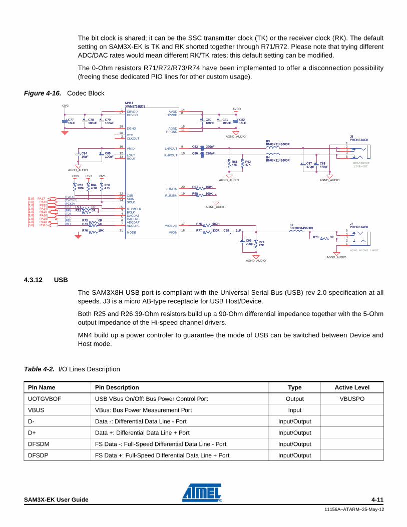
The bit clock is shared; it can be the SSC transmitter clock (TK) or the receiver clock (RK). The default setting on SAM3X-EK is TK and RK shorted together through R71/R72. Please note that trying different ADC/DAC rates would mean different RK/TK rates; this default setting can be modified.
The 0-Ohm resistors R71/R72/R73/R74 have been implemented to offer a disconnection possibility (freeing these dedicated PIO lines for other custom usage).
Figure 4-16. Codec Block
4.3.12 USB
The SAM3X8H USB port is compliant with the Universal Serial Bus (USB) rev 2.0 specification at all speeds. J3 is a micro AB-type receptacle for USB Host/Device.
Both R25 and R26 39-Ohm resistors build up a 90-Ohm differential impedance together with the 5-Ohm output impedance of the Hi-speed channel drivers.
MN4 build up a power controler to guarantee the mode of USB can be switched between Device and Host mode.
Table 4-2. I/O Lines Description
HEADPHONELINE-OUT
MONO MICRO INPUT
(TWD0)(TWCK0)(PCK0)
(TD)(TF)(RD)(RF)
(TK)(RF)
+3V3
+3V3 +3V3 +3V3
AVDD
AGND_AUDIOAGND_AUDIO
AGND_AUDIO
AGND_AUDIO
AGND_AUDIO
AGND_AUDIO
AGND_AUDIO
PA18[3,8]PB22[3,8]PA14[3,8]
PA15[3,8]PA16[3,8]
PA17[3,8]
PB19[3,8]
PB18[3,8]PB17[3,8]
R644.7KR644.7K
C81100nFC81100nF
B3BN03K314S600RB3BN03K314S600R
R6247KR6247K
R78 0RR78 0R
R77 330RR77 330R
R664.7KR664.7K
J7PHONEJACKJ7PHONEJACK
54321
+ C8210uF
+ C8210uF
MN11XWM8731EDSMN11XWM8731EDS
DBVDD1
CLKOUT2
BCLK3
DACDAT4
DACLRC5
ADCDAT6
ADCLRC7
HPVDD8
LHPOUT9
RHPOUT10
HPGND11
LOUT12
ROUT13
AVDD14
AGND15
VMID16
MICBIAS17
MICIN18
RLINEIN19
LLINEIN20
MODE21
CSB22
SDIN23
SCLK24
XTI/MCLK25
XTO26
DCVDD27
DGND28
C88470pFC88470pF
R75 680RR75 680R
R67 100KR67 100K
R7947KR7947K
C78100nFC78100nF
+ C7710uF
+ C7710uF
B4BN03K314S600RB4BN03K314S600R
R63100KR63100K
R68 100KR68 100K
B7BN03K314S600RB7BN03K314S600R
R74 0RR74 0R
+C86 220uF+C86 220uF
C87470pFC87470pF
R6147KR6147K
J5PHONEJACKJ5PHONEJACK
54321
+ C8410uF
+ C8410uF
R73 0RR73 0R
C80100nFC80100nF
+C83 220uF+C83 220uF
C79100nFC79100nF
R71 0RR71 0R
C98 1uFC98 1uF
C85100nFC85100nF
R72 0RR72 0R
C99220pFC99220pF
R76 10KR76 10K
PIn Name Pin Description Type Active Level
UOTGVBOF USB VBus On/Off: Bus Power Control Port Output VBUSPO
VBUS VBus: Bus Power Measurement Port Input
D- Data -: Differential Data Line - Port Input/Output
D+ Data +: Differential Data Line + Port Input/Output
DFSDM FS Data -: Full-Speed Differential Data Line - Port Input/Output
DFSDP FS Data +: Full-Speed Differential Data Line + Port Input/Output
SAM3X-EK User Guide 4-11
11156A–ATARM–25-May-12
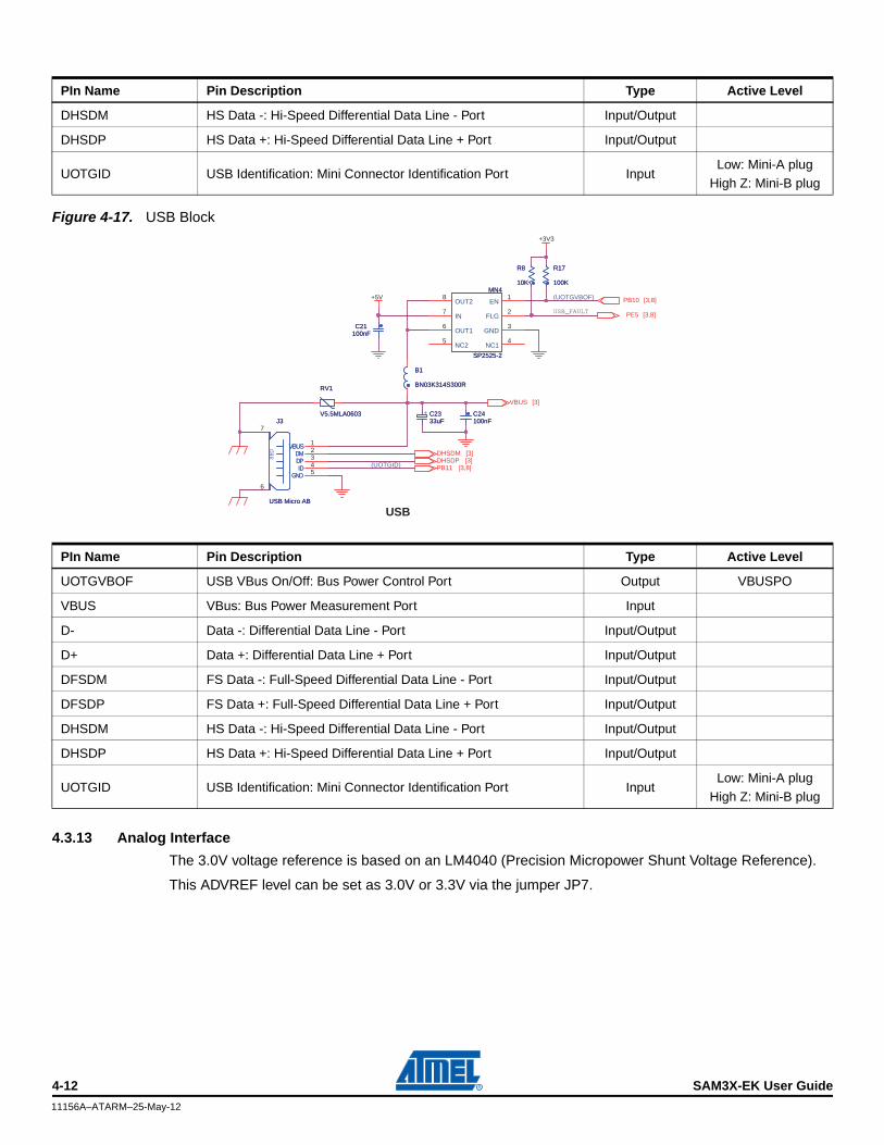
Figure 4-17. USB Block
4.3.13 Analog InterfaceThe 3.0V voltage reference is based on an LM4040 (Precision Micropower Shunt Voltage Reference).
This ADVREF level can be set as 3.0V or 3.3V via the jumper JP7.
DHSDM HS Data -: Hi-Speed Differential Data Line - Port Input/Output
DHSDP HS Data +: Hi-Speed Differential Data Line + Port Input/Output
UOTGID USB Identification: Mini Connector Identification Port InputLow: Mini-A plug
High Z: Mini-B plug
PIn Name Pin Description Type Active Level
UOTGVBOF USB VBus On/Off: Bus Power Control Port Output VBUSPO
VBUS VBus: Bus Power Measurement Port Input
D- Data -: Differential Data Line - Port Input/Output
D+ Data +: Differential Data Line + Port Input/Output
DFSDM FS Data -: Full-Speed Differential Data Line - Port Input/Output
DFSDP FS Data +: Full-Speed Differential Data Line + Port Input/Output
DHSDM HS Data -: Hi-Speed Differential Data Line - Port Input/Output
DHSDP HS Data +: Hi-Speed Differential Data Line + Port Input/Output
UOTGID USB Identification: Mini Connector Identification Port InputLow: Mini-A plug
High Z: Mini-B plug
PIn Name Pin Description Type Active Level
USB
(UOTGVBOF)
(UOTGID)
USB_FAULT
+5V
+3V3
PE5 [3,8]
PB10 [3,8]
DHSDM [3]DHSDP [3]PB11 [3,8]
VBUS [3]
B1
BN03K314S300R
B1
BN03K314S300R
VBUS
SHD DM
DPID
GND
J3
USB Micro AB
VBUS
SHD DM
DPID
GND
J3
USB Micro AB
12345
7
6
C24100nFC24100nF
RV1
V5.5MLA0603
RV1
V5.5MLA0603
MN4
SP2525-2
MN4
SP2525-2
EN1
FLG2
NC14
OUT28
OUT16
IN7
NC25
GND3
R8
10K
R8
10K
C21100nFC21
100nF
R17
100K
R17
100K
+ C2333uF
+ C2333uF
4-12 SAM3X-EK User Guide
11156A–ATARM–25-May-12
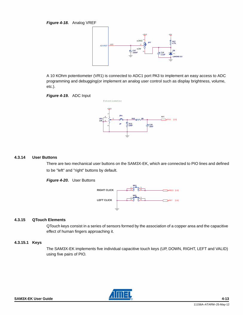
Figure 4-18. Analog VREF
A 10 KOhm potentiometer (VR1) is connected to ADC1 port PA3 to implement an easy access to ADC programming and debugging(or implement an analog user control such as display brightness, volume, etc.).
Figure 4-19. ADC Input
4.3.14 User Buttons
There are two mechanical user buttons on the SAM3X-EK, which are connected to PIO lines and defined
to be "left" and "right" buttons by default.
Figure 4-20. User Buttons
4.3.15 QTouch Elements
QTouch keys consist in a series of sensors formed by the association of a copper area and the capacitive effect of human fingers approaching it.
4.3.15.1 Keys
The SAM3X-EK implements five individual capacitive touch keys (UP, DOWN, RIGHT, LEFT and VALID) using five pairs of PIO.
+3V3
+3V
+3V3 +5V
R274.7KR274.7K
ADVREFU15
C162.2uFC162.2uF
JP7JP7
1
2
3C47100nFC47100nF
D6
LM4040-3.0
D6
LM4040-3.0
AD1
Potentiometer
+3V3
PA3 [3,8]
R15DNPR15DNP C20
10nFC2010nF
VR110KVR110K
13
24
5R35 0RR35 0R
JP4
JP
JP4
JP
RIGHT CLICK
LEFT CLICK
PB23 [3,8]
PE7 [3,8]
BP4BP41
423
BP5BP51
423
SAM3X-EK User Guide 4-13
11156A–ATARM–25-May-12
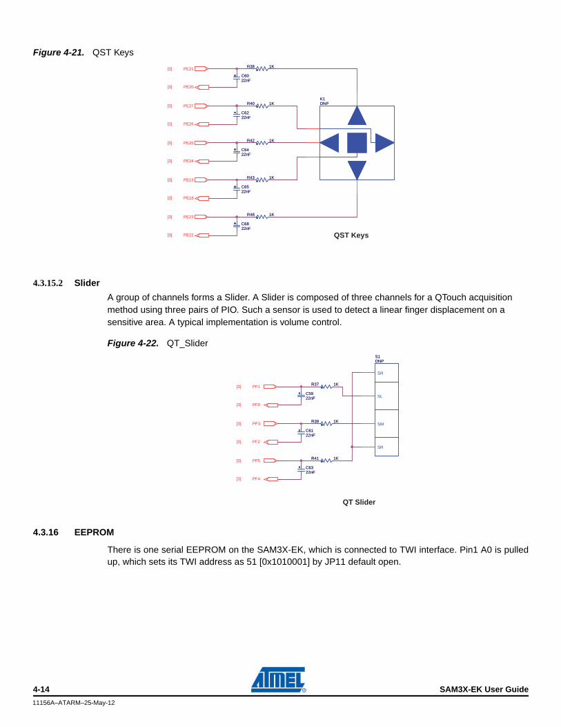
Figure 4-21. QST Keys
4.3.15.2 Slider
A group of channels forms a Slider. A Slider is composed of three channels for a QTouch acquisition method using three pairs of PIO. Such a sensor is used to detect a linear finger displacement on a sensitive area. A typical implementation is volume control.
Figure 4-22. QT_Slider
4.3.16 EEPROM
There is one serial EEPROM on the SAM3X-EK, which is connected to TWI interface. Pin1 A0 is pulled up, which sets its TWI address as 51 [0x1010001] by JP11 default open.
QST Keys
PE20[3]
PE21[3]
PE26[3]
PE27[3]
PE24[3]
PE25[3]
PE18[3]
PE19[3]
PE22[3]
PE23[3]
C6222nFC6222nF
C6522nFC6522nF
C6822nFC6822nF
R42 1KR42 1K
R48 1KR48 1K
K1DNPK1DNPR40 1KR40 1K
R43 1KR43 1K
C6022nFC6022nF
R38 1KR38 1K
C6422nFC6422nF
QT Slider
PF0[3]
PF1[3]
PF2[3]
PF3[3]
PF4[3]
PF5[3]
R39 1KR39 1K
R41 1KR41 1K
C6322nFC6322nF
C6122nFC6122nF
C5922nFC5922nF
S1DNPS1DNP
SL
SM
SR
SR
R37 1KR37 1K
4-14 SAM3X-EK User Guide
11156A–ATARM–25-May-12
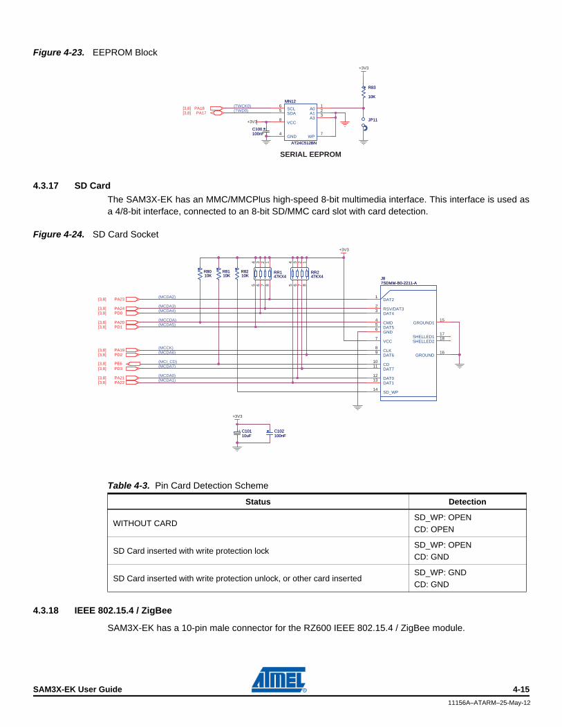
Figure 4-23. EEPROM Block
4.3.17 SD Card
The SAM3X-EK has an MMC/MMCPlus high-speed 8-bit multimedia interface. This interface is used as a 4/8-bit interface, connected to an 8-bit SD/MMC card slot with card detection.
Figure 4-24. SD Card Socket
4.3.18 IEEE 802.15.4 / ZigBee
SAM3X-EK has a 10-pin male connector for the RZ600 IEEE 802.15.4 / ZigBee module.
SERIAL EEPROM
(TWCK0)(TWD0)
+3V3
+3V3
PA18[3,8]PA17[3,8]
R83
10K
R83
10K
C100100nFC100100nF
MN12
AT24C512BN
MN12
AT24C512BN
A01
A12
WP7
SCL6
VCC8 A3
3SDA5
GND4
JP11JP11
(MCCK)(MCDA6)
(MCCDA)
(MCDA2)
(MCDA3)(MCDA4)
(MCDA5)
(MCDA7)
(MCDA0)(MCDA1)
(MCI_CD)
+3V3
+3V3
PD0[3,8]PA24[3,8]
PD1[3,8]PA20[3,8]
PA23[3,8]
PD3[3,8]
PA22[3,8]PA21[3,8]
PD2[3,8]PA19[3,8]
PE6[3,8]
R8010KR8010K
R8110KR8110K
RR147KX4RR147KX4
12345 6 7 8
R8210KR8210K
J87SDMM-B0-2211-AJ87SDMM-B0-2211-A
DAT21
RSV/DAT32
DAT43
CMD4
DAT55
GND6
VCC7
CLK8
DAT69
CD10
DAT711
DAT012
DAT113
SD_WP14
GROUND115
GROUND16
SHELLED117
SHELLED218
RR247KX4RR247KX4
12345 6 7 8
C102100nFC102100nF
+ C10110uF
+ C10110uF
Table 4-3. Pin Card Detection Scheme
Status Detection
WITHOUT CARDSD_WP: OPEN CD: OPEN
SD Card inserted with write protection lockSD_WP: OPEN CD: GND
SD Card inserted with write protection unlock, or other card insertedSD_WP: GND CD: GND
SAM3X-EK User Guide 4-15
11156A–ATARM–25-May-12
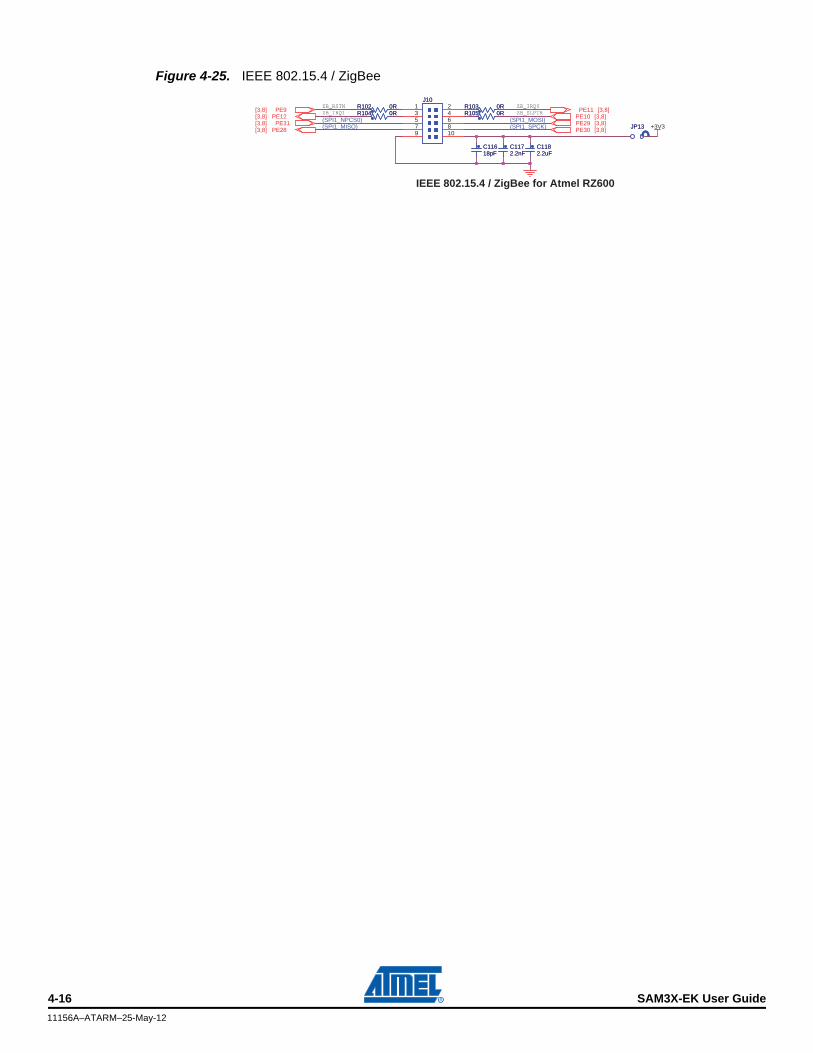
Figure 4-25. IEEE 802.15.4 / ZigBee
IEEE 802.15.4 / ZigBee for Atmel RZ600
(SPI1_NPCS0)(SPI1_MISO)
(SPI1_MOSI)(SPI1_SPCK)
ZB_IRQ0ZB_IRQ1ZB_RSTN
ZB_SLPTR
+3V3PE28[3,8]PE29 [3,8]PE30 [3,8]
PE31[3,8]
PE9[3,8]PE10 [3,8]
PE11 [3,8]PE12[3,8]
C1172.2nFC1172.2nF
R102 0RR102 0R R103 0RR103 0RR105 0RR105 0R
C11618pFC11618pF
R104 0RR104 0R
J10J101 23 45 67 89 10
C1182.2uFC1182.2uF
JP13JP13
4-16 SAM3X-EK User Guide
11156A–ATARM–25-May-12
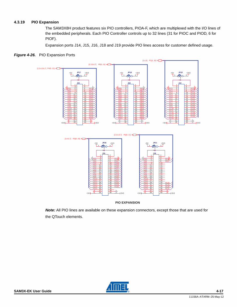
4.3.19 PIO Expansion
The SAM3X8H product features six PIO controllers, PIOA-F, which are multiplexed with the I/O lines of the embedded peripherals. Each PIO Controller controls up to 32 lines (31 for PIOC and PIOD, 6 for PIOF).
Expansion ports J14, J15, J16, J18 and J19 provide PIO lines access for customer defined usage.
Figure 4-26. PIO Expansion Ports
Note: All PIO lines are available on these expansion connectors, except those that are used for
the QTouch elements.
PIO EXPANSION
PA18PA19PA20
PA6
PA9
PA11
PA14PA13
PA7PA8
PA12
PA10
PA15
PA22
PA27
PA23
PA29PA30
PA25
PA21
PA28
PA24
PA26
PA31
PA16PA17
PA0PA1PA2PA3PA4PA5
PB18PB19PB20
PB6
PB9
PB11
PB14PB13
PB7PB8
PB12
PB10
PB15
PB22
PB27
PB23
PB29PB30
PB25
PB21
PB28
PB24
PB26
PB31
PB16PB17
PB0PB1PB2PB3PB4PB5
PC18PC19PC20
PC6
PC9
PC11
PC14PC13
PC7PC8
PC12
PC10
PC15
PC22
PC27
PC23
PC29PC30
PC25
PC21
PC28
PC24
PC26
PC16PC17
PC0PC1PC2PC3PC4PC5
PD18PD19PD20
PD6
PD9
PD11
PD14PD13
PD7PD8
PD12
PD10
PD15
PD22
PD27
PD23
PD29PD30
PD25
PD21
PD28
PD24
PD26
PD16PD17
PD0PD1PD2PD3PD4PD5
PE6
PE9
PE11
PE14PE13
PE7PE8
PE12
PE10
PE15
PE29PE30
PE28
PE31
PE16PE0PE1PE2PE3PE4PE5
PE17
+3V3+5V
+3V3+3V3 +3V3
+3V3+5V
+3V3 +3V3
+3V3+5V
+3V3
+3V3
+3V3+5V
+3V3 +3V3
+3V3+5V
+3V3
PA[0..31]
PB[0..31][2,3,5,6,7]
PC[0..30][3,4,5]
PD[0..30][3,4,6,7]
PE[0..31][2,3,5,6,7]
JP17JP171
23
J19J191 23 45 67 89 10
11 1213 1415 1617 1819 2021 2223 2425 2627 2829 3031 3233 3435 3637 3839 40
J16J161 23 45 67 89 10
11 1213 1415 1617 1819 2021 2223 2425 2627 2829 3031 3233 3435 3637 3839 40
JP21JP211
2
3
J15J151 23 45 67 89 10
11 1213 1415 1617 1819 2021 2223 2425 2627 2829 3031 3233 3435 3637 3839 40
JP18JP181
2
3
J14J141 23 45 67 89 10
11 1213 1415 1617 1819 2021 2223 2425 2627 2829 3031 3233 3435 3637 3839 40
JP20JP201
2
3
J18J181 23 45 67 89 10
11 1213 1415 1617 1819 2021 2223 2425 2627 2829 3031 3233 3435 3637 3839 40
JP19JP191
2
3
[2,3,4,5,6,7]
SAM3X-EK User Guide 4-17
11156A–ATARM–25-May-12
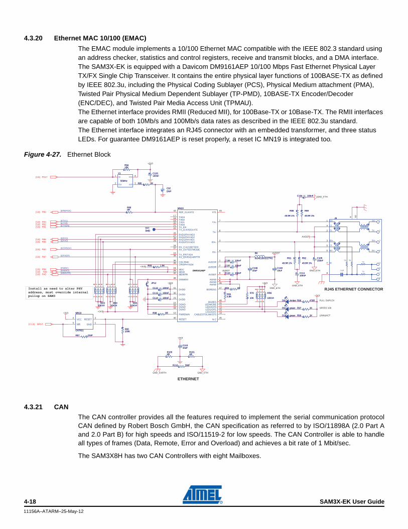
4.3.20 Ethernet MAC 10/100 (EMAC)The EMAC module implements a 10/100 Ethernet MAC compatible with the IEEE 802.3 standard using an address checker, statistics and control registers, receive and transmit blocks, and a DMA interface. The SAM3X-EK is equipped with a Davicom DM9161AEP 10/100 Mbps Fast Ethernet Physical Layer TX/FX Single Chip Transceiver. It contains the entire physical layer functions of 100BASE-TX as defined by IEEE 802.3u, including the Physical Coding Sublayer (PCS), Physical Medium attachment (PMA), Twisted Pair Physical Medium Dependent Sublayer (TP-PMD), 10BASE-TX Encoder/Decoder (ENC/DEC), and Twisted Pair Media Access Unit (TPMAU).The Ethernet interface provides RMII (Reduced MII), for 100Base-TX or 10Base-TX. The RMII interfaces are capable of both 10Mb/s and 100Mb/s data rates as described in the IEEE 802.3u standard. The Ethernet interface integrates an RJ45 connector with an embedded transformer, and three statusLEDs. For guarantee DM9161AEP is reset properly, a reset IC MN19 is integrated too.
Figure 4-27. Ethernet Block
4.3.21 CAN
The CAN controller provides all the features required to implement the serial communication protocol CAN defined by Robert Bosch GmbH, the CAN specification as referred to by ISO/11898A (2.0 Part A and 2.0 Part B) for high speeds and ISO/11519-2 for low speeds. The CAN Controller is able to handle all types of frames (Data, Remote, Error and Overload) and achieves a bit rate of 1 Mbit/sec.
The SAM3X8H has two CAN Controllers with eight Mailboxes.
(ERX1)(ERX0)
RJ45 ETHERNET CONNECTOR
(ETX1)(ETX0)(ETXEN)
(EMDC)(EMDIO)(MDINTR)
(ERXER)
SPEED 100
FULL DUPLEX
LINK&ACT
(EREFCK)
Install as need to alter PHYaddress, must override internalpullup on SAM3
ETHERNET
(ECRSDV)
+3V3
+3V3
+3V3
+3V3
+3V3
+3V3GND_ETH
GND_ETH
GND_ETH
GND_ETHGND_EARTH
GND_ETH
AVDDT
AVDDT
AVDDT
+3V3+3V3
PB9[3,8]PA5[3,8]
PB7[3,8]
PB5[3,8]PB6[3,8]
PB0[3,8]
PB3[3,8]PB2[3,8]PB1[3,8]
PB8[3,8]
PB4[3,8]
NRST[2,3,5]
PD17[3,8]
R956.8KR956.8K
C113 100nFC113 100nF
R116 DNPR116 DNP
VDD
VSS OUT
OE
Y3
50MHz
VDD
VSS OUT
OE
Y3
50MHz
41
32
C92DNPC92DNP
R1000RR1000R
C103100nFC103100nF
D10 greenD10 green
1
2
3
6
4
5
7
8
75
75
7575
1nF
TD+
TD-
CT
NC
RD-
CT
TX+
TX-
RX+
RX-
RD+
J91
2
3
6
4
5
7
8
75
75
7575
1nF
TD+
TD-
CT
NC
RD-
CT
TX+
TX-
RX+
RX-
RD+
J91
2
7
8
3
6
5
4
9 10
R87 DNPR87 DNP
R90100KR90100K
R93 1.5KR93 1.5K
R94 0RR94 0R
C104 100nFC104 100nF
MN13
DM9161AEP
MN13
DM9161AEP
TX_ER/TXD416
COL/RMII36
MDC24
RX-4
RX+3
TX-8
TX+7
XT143
REF_CLK/XT242
RX_CLK/10BTSER34
RX_DV/TESTMODE37
RX_ER/RXD4/RPTR38
TX_EN21
BGRES48
AVDDR1
AVDDR2
DVDD41
DGND44
DGND15
AGND5
AGND6
LED2/OP213LED1/OP112LED0/OP011
TXD317
TXD218
TXD020 TXD119
TX_CLK/ISOLATE22
RXD0/PHYAD029 RXD1/PHYAD128 RXD2/PHYAD227 RXD3/PHYAD326
CRS/PHYAD435
MDIO25
MDINTR32
PWRDWN10
DGND33
RESET40
AVDDT9
DISMDIX39
DVDD30
DVDD23
AGND46
BGRESG47
CABLESTS/LINKSTS14
N.C45
LEDMODE31
R96 470RR96 470R
R99 1KR99 1K
R91
49.9R 1%
R91
49.9R 1%
JP12JP12
RR410KX4
RR410KX4
1 2 3 45678
C106 100nFC106 100nF
C114 100nFC114 100nF
R98 0RR98 0R
+ C10810uF
+ C10810uF
MN19
CAT811
MN19
CAT811
GND1
RESET2
MR3
VCC4
R89
49.9R 1%
R89
49.9R 1%
R88
49.9R 1%
R88
49.9R 1%
C111100nFC111100nF
RR6
10KX4
RR6
10KX4
1 2 3 45678
R70
10K
R70
10K
R85 0RR85 0R
+ C10910uF
+ C10910uF
C112 100nFC112 100nF
TP7SMDTP7SMD
+ C11510uF
+ C11510uF
R860RR860R
B8
BLM21BD222TN1
B8
BLM21BD222TN1
D9 greenD9 green
R8410KR8410K
RR310KX4
RR310KX4
1 2 3 45678
C110 100nFC110 100nF
R1010RR1010R
D8 AmberD8 AmberRR5
10KX4RR5
10KX4
1 2 3 45678
R92
49.9R 1%
R92
49.9R 1%C107 100nFC107 100nF
R97 1KR97 1K
C105100nFC105100nF
4-18 SAM3X-EK User Guide
11156A–ATARM–25-May-12
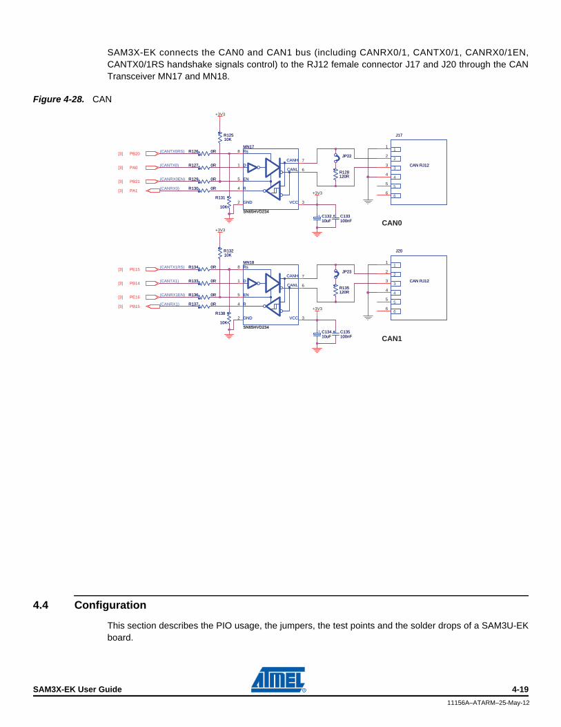
SAM3X-EK connects the CAN0 and CAN1 bus (including CANRX0/1, CANTX0/1, CANRX0/1EN, CANTX0/1RS handshake signals control) to the RJ12 female connector J17 and J20 through the CAN Transceiver MN17 and MN18.
Figure 4-28. CAN
4.4 Configuration
This section describes the PIO usage, the jumpers, the test points and the solder drops of a SAM3U-EK board.
(CANTX0)
(CANRX0)
(CANTX0RS)
(CANRX0EN)
(CANRX1)
(CANTX1RS)
(CANRX1EN)
(CANTX1)
CAN0
CAN1
+3V3
+3V3
+3V3
+3V3
PA1[3]
PB20[3]
PA0[3]
PB21[3]
PB15[3]
PE15[3]
PB14[3]
PE16[3]
R134 0RR134 0R
JP22JP22
+ C13210uF
+ C13210uF
C135100nFC135100nF
J20
CAN RJ12
J20
CAN RJ12
11
22
33
44
55
66
R130 0RR130 0R
R138
10K
R138
10K
R13210KR13210K
R135120RR135120R
R12510KR12510K
R129 0RR129 0R
R128120RR128120R
R127 0RR127 0R
Rs
D
EN
R
CANH
CANL
VCCGND
MN18
SN65HVD234
Rs
D
EN
R
CANH
CANL
VCCGND
MN18
SN65HVD234
2 3
7
6
4
1
5
8
R137 0RR137 0R
R126 0RR126 0R
C133100nFC133100nF
R133 0RR133 0R
JP23JP23
R131
10K
R131
10K
R136 0RR136 0R
+ C13410uF
+ C13410uF
J17
CAN RJ12
J17
CAN RJ12
11
22
33
44
55
66
Rs
D
EN
R
CANH
CANL
VCCGND
MN17
SN65HVD234
Rs
D
EN
R
CANH
CANL
VCCGND
MN17
SN65HVD234
2 3
7
6
4
1
5
8
SAM3X-EK User Guide 4-19
11156A–ATARM–25-May-12
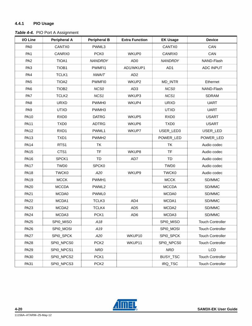
4.4.1 PIO Usage
Table 4-4. PIO Port A Assignment
I/O Line Peripheral A Peripheral B Extra Function EK Usage Device
PA0 CANTX0 PWML3 CANTX0 CAN
PA1 CANRX0 PCK0 WKUP0 CANRX0 CAN
PA2 TIOA1 NANDRDY AD0 NANDRDY NAND-Flash
PA3 TIOB1 PWMFI1 AD1/WKUP1 AD1 ADC INPUT
PA4 TCLK1 NWAIT AD2
PA5 TIOA2 PWMFI0 WKUP2 MD_INTR Ethernet
PA6 TIOB2 NCS0 AD3 NCS0 NAND-Flash
PA7 TCLK2 NCS1 WKUP3 NCS1 SDRAM
PA8 URXD PWMH0 WKUP4 URXD UART
PA9 UTXD PWMH3 UTXD UART
PA10 RXD0 DATRG WKUP5 RXD0 USART
PA11 TXD0 ADTRG WKUP6 TXD0 USART
PA12 RXD1 PWML1 WKUP7 USER_LED3 USER_LED
PA13 TXD1 PWMH2 POWER_LED POWER_LED
PA14 RTS1 TK TK Audio codec
PA15 CTS1 TF WKUP8 TF Audio codec
PA16 SPCK1 TD AD7 TD Audio codec
PA17 TWD0 SPCK0 TWD0 Audio codec
PA18 TWCK0 A20 WKUP9 TWCK0 Audio codec
PA19 MCCK PWMH1 MCCK SD/MMC
PA20 MCCDA PWML2 MCCDA SD/MMC
PA21 MCDA0 PWML0 MCDA0 SD/MMC
PA22 MCDA1 TCLK3 AD4 MCDA1 SD/MMC
PA23 MCDA2 TCLK4 AD5 MCDA2 SD/MMC
PA24 MCDA3 PCK1 AD6 MCDA3 SD/MMC
PA25 SPI0_MISO A18 SPI0_MISO Touch Controller
PA26 SPI0_MOSI A19 SPI0_MOSI Touch Controller
PA27 SPI0_SPCK A20 WKUP10 SPI0_SPCK Touch Controller
PA28 SPI0_NPCS0 PCK2 WKUP11 SPI0_NPCS0 Touch Controller
PA29 SPI0_NPCS1 NRD NRD LCD
PA30 SPI0_NPCS2 PCK1 BUSY_TSC Touch Controller
PA31 SPI0_NPCS3 PCK2 IRQ_TSC Touch Controller
4-20 SAM3X-EK User Guide
11156A–ATARM–25-May-12
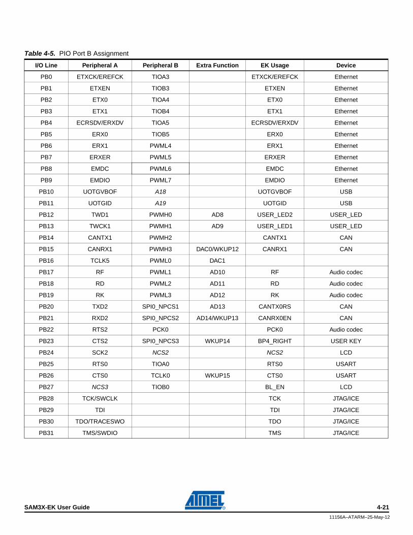
Table 4-5. PIO Port B Assignment
I/O Line Peripheral A Peripheral B Extra Function EK Usage Device
PB0 ETXCK/EREFCK TIOA3 ETXCK/EREFCK Ethernet
PB1 ETXEN TIOB3 ETXEN Ethernet
PB2 ETX0 TIOA4 ETX0 Ethernet
PB3 ETX1 TIOB4 ETX1 Ethernet
PB4 ECRSDV/ERXDV TIOA5 ECRSDV/ERXDV Ethernet
PB5 ERX0 TIOB5 ERX0 Ethernet
PB6 ERX1 PWML4 ERX1 Ethernet
PB7 ERXER PWML5 ERXER Ethernet
PB8 EMDC PWML6 EMDC Ethernet
PB9 EMDIO PWML7 EMDIO Ethernet
PB10 UOTGVBOF A18 UOTGVBOF USB
PB11 UOTGID A19 UOTGID USB
PB12 TWD1 PWMH0 AD8 USER_LED2 USER_LED
PB13 TWCK1 PWMH1 AD9 USER_LED1 USER_LED
PB14 CANTX1 PWMH2 CANTX1 CAN
PB15 CANRX1 PWMH3 DAC0/WKUP12 CANRX1 CAN
PB16 TCLK5 PWML0 DAC1
PB17 RF PWML1 AD10 RF Audio codec
PB18 RD PWML2 AD11 RD Audio codec
PB19 RK PWML3 AD12 RK Audio codec
PB20 TXD2 SPI0_NPCS1 AD13 CANTX0RS CAN
PB21 RXD2 SPI0_NPCS2 AD14/WKUP13 CANRX0EN CAN
PB22 RTS2 PCK0 PCK0 Audio codec
PB23 CTS2 SPI0_NPCS3 WKUP14 BP4_RIGHT USER KEY
PB24 SCK2 NCS2 NCS2 LCD
PB25 RTS0 TIOA0 RTS0 USART
PB26 CTS0 TCLK0 WKUP15 CTS0 USART
PB27 NCS3 TIOB0 BL_EN LCD
PB28 TCK/SWCLK TCK JTAG/ICE
PB29 TDI TDI JTAG/ICE
PB30 TDO/TRACESWO TDO JTAG/ICE
PB31 TMS/SWDIO TMS JTAG/ICE
SAM3X-EK User Guide 4-21
11156A–ATARM–25-May-12
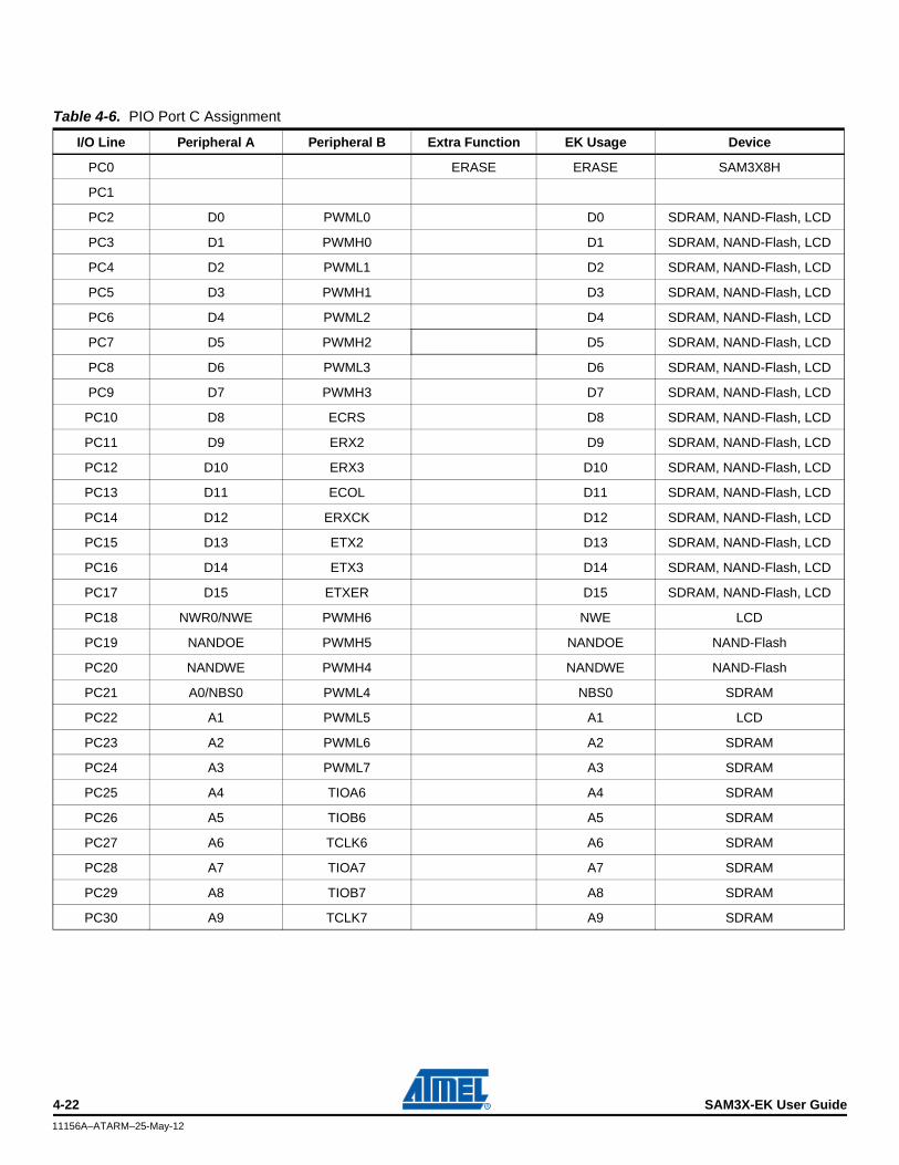
Table 4-6. PIO Port C Assignment
I/O Line Peripheral A Peripheral B Extra Function EK Usage Device
PC0 ERASE ERASE SAM3X8H
PC1
PC2 D0 PWML0 D0 SDRAM, NAND-Flash, LCD
PC3 D1 PWMH0 D1 SDRAM, NAND-Flash, LCD
PC4 D2 PWML1 D2 SDRAM, NAND-Flash, LCD
PC5 D3 PWMH1 D3 SDRAM, NAND-Flash, LCD
PC6 D4 PWML2 D4 SDRAM, NAND-Flash, LCD
PC7 D5 PWMH2 D5 SDRAM, NAND-Flash, LCD
PC8 D6 PWML3 D6 SDRAM, NAND-Flash, LCD
PC9 D7 PWMH3 D7 SDRAM, NAND-Flash, LCD
PC10 D8 ECRS D8 SDRAM, NAND-Flash, LCD
PC11 D9 ERX2 D9 SDRAM, NAND-Flash, LCD
PC12 D10 ERX3 D10 SDRAM, NAND-Flash, LCD
PC13 D11 ECOL D11 SDRAM, NAND-Flash, LCD
PC14 D12 ERXCK D12 SDRAM, NAND-Flash, LCD
PC15 D13 ETX2 D13 SDRAM, NAND-Flash, LCD
PC16 D14 ETX3 D14 SDRAM, NAND-Flash, LCD
PC17 D15 ETXER D15 SDRAM, NAND-Flash, LCD
PC18 NWR0/NWE PWMH6 NWE LCD
PC19 NANDOE PWMH5 NANDOE NAND-Flash
PC20 NANDWE PWMH4 NANDWE NAND-Flash
PC21 A0/NBS0 PWML4 NBS0 SDRAM
PC22 A1 PWML5 A1 LCD
PC23 A2 PWML6 A2 SDRAM
PC24 A3 PWML7 A3 SDRAM
PC25 A4 TIOA6 A4 SDRAM
PC26 A5 TIOB6 A5 SDRAM
PC27 A6 TCLK6 A6 SDRAM
PC28 A7 TIOA7 A7 SDRAM
PC29 A8 TIOB7 A8 SDRAM
PC30 A9 TCLK7 A9 SDRAM
4-22 SAM3X-EK User Guide
11156A–ATARM–25-May-12
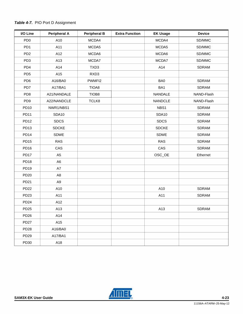
Table 4-7. PIO Port D Assignment
I/O Line Peripheral A Peripheral B Extra Function EK Usage Device
PD0 A10 MCDA4 MCDA4 SD/MMC
PD1 A11 MCDA5 MCDA5 SD/MMC
PD2 A12 MCDA6 MCDA6 SD/MMC
PD3 A13 MCDA7 MCDA7 SD/MMC
PD4 A14 TXD3 A14 SDRAM
PD5 A15 RXD3
PD6 A16/BA0 PWMFI2 BA0 SDRAM
PD7 A17/BA1 TIOA8 BA1 SDRAM
PD8 A21/NANDALE TIOB8 NANDALE NAND-Flash
PD9 A22/NANDCLE TCLK8 NANDCLE NAND-Flash
PD10 NWR1/NBS1 NBS1 SDRAM
PD11 SDA10 SDA10 SDRAM
PD12 SDCS SDCS SDRAM
PD13 SDCKE SDCKE SDRAM
PD14 SDWE SDWE SDRAM
PD15 RAS RAS SDRAM
PD16 CAS CAS SDRAM
PD17 A5 OSC_OE Ethernet
PD18 A6
PD19 A7
PD20 A8
PD21 A9
PD22 A10 A10 SDRAM
PD23 A11 A11 SDRAM
PD24 A12
PD25 A13 A13 SDRAM
PD26 A14
PD27 A15
PD28 A16/BA0
PD29 A17/BA1
PD30 A18
SAM3X-EK User Guide 4-23
11156A–ATARM–25-May-12
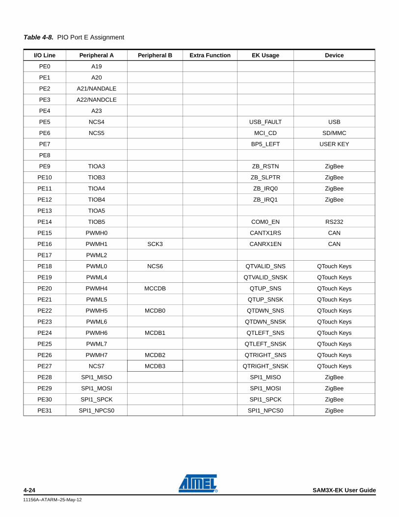
Table 4-8. PIO Port E Assignment
I/O Line Peripheral A Peripheral B Extra Function EK Usage Device
PE0 A19
PE1 A20
PE2 A21/NANDALE
PE3 A22/NANDCLE
PE4 A23
PE5 NCS4 USB_FAULT USB
PE6 NCS5 MCI_CD SD/MMC
PE7 BP5_LEFT USER KEY
PE8
PE9 TIOA3 ZB_RSTN ZigBee
PE10 TIOB3 ZB_SLPTR ZigBee
PE11 TIOA4 ZB_IRQ0 ZigBee
PE12 TIOB4 ZB_IRQ1 ZigBee
PE13 TIOA5
PE14 TIOB5 COM0_EN RS232
PE15 PWMH0 CANTX1RS CAN
PE16 PWMH1 SCK3 CANRX1EN CAN
PE17 PWML2
PE18 PWML0 NCS6 QTVALID_SNS QTouch Keys
PE19 PWML4 QTVALID_SNSK QTouch Keys
PE20 PWMH4 MCCDB QTUP_SNS QTouch Keys
PE21 PWML5 QTUP_SNSK QTouch Keys
PE22 PWMH5 MCDB0 QTDWN_SNS QTouch Keys
PE23 PWML6 QTDWN_SNSK QTouch Keys
PE24 PWMH6 MCDB1 QTLEFT_SNS QTouch Keys
PE25 PWML7 QTLEFT_SNSK QTouch Keys
PE26 PWMH7 MCDB2 QTRIGHT_SNS QTouch Keys
PE27 NCS7 MCDB3 QTRIGHT_SNSK QTouch Keys
PE28 SPI1_MISO SPI1_MISO ZigBee
PE29 SPI1_MOSI SPI1_MOSI ZigBee
PE30 SPI1_SPCK SPI1_SPCK ZigBee
PE31 SPI1_NPCS0 SPI1_NPCS0 ZigBee
4-24 SAM3X-EK User Guide
11156A–ATARM–25-May-12
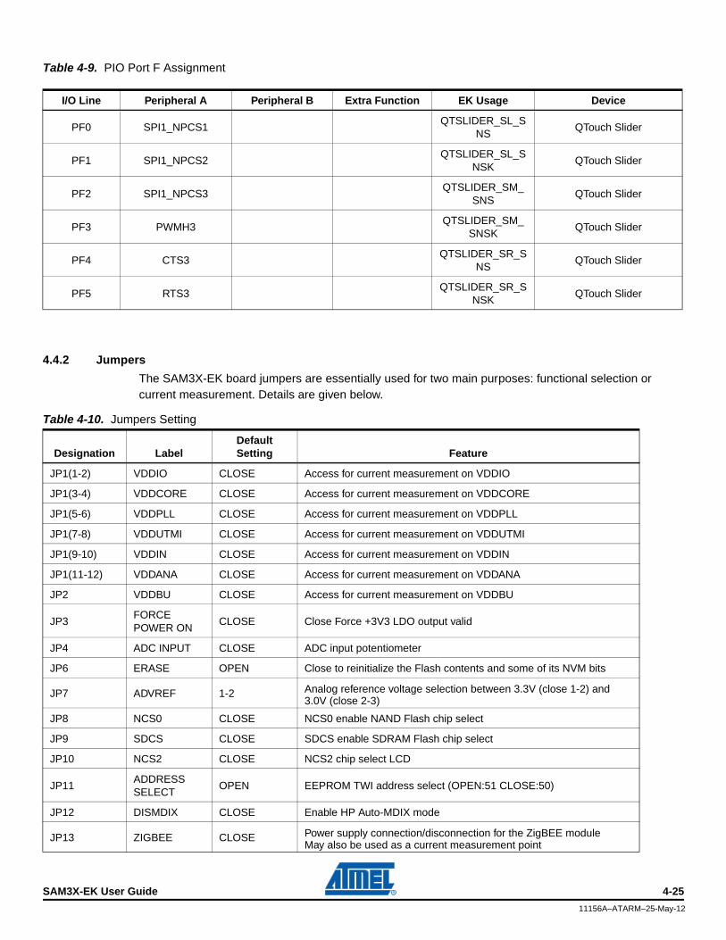
Table 4-9. PIO Port F Assignment
4.4.2 Jumpers
The SAM3X-EK board jumpers are essentially used for two main purposes: functional selection or current measurement. Details are given below.
I/O Line Peripheral A Peripheral B Extra Function EK Usage Device
PF0 SPI1_NPCS1QTSLIDER_SL_S
NSQTouch Slider
PF1 SPI1_NPCS2QTSLIDER_SL_S
NSKQTouch Slider
PF2 SPI1_NPCS3QTSLIDER_SM_
SNSQTouch Slider
PF3 PWMH3QTSLIDER_SM_
SNSKQTouch Slider
PF4 CTS3QTSLIDER_SR_S
NSQTouch Slider
PF5 RTS3QTSLIDER_SR_S
NSKQTouch Slider
Table 4-10. Jumpers Setting
Designation LabelDefault Setting Feature
JP1(1-2) VDDIO CLOSE Access for current measurement on VDDIO
JP1(3-4) VDDCORE CLOSE Access for current measurement on VDDCORE
JP1(5-6) VDDPLL CLOSE Access for current measurement on VDDPLL
JP1(7-8) VDDUTMI CLOSE Access for current measurement on VDDUTMI
JP1(9-10) VDDIN CLOSE Access for current measurement on VDDIN
JP1(11-12) VDDANA CLOSE Access for current measurement on VDDANA
JP2 VDDBU CLOSE Access for current measurement on VDDBU
JP3FORCE POWER ON
CLOSE Close Force +3V3 LDO output valid
JP4 ADC INPUT CLOSE ADC input potentiometer
JP6 ERASE OPEN Close to reinitialize the Flash contents and some of its NVM bits
JP7 ADVREF 1-2 Analog reference voltage selection between 3.3V (close 1-2) and3.0V (close 2-3)
JP8 NCS0 CLOSE NCS0 enable NAND Flash chip select
JP9 SDCS CLOSE SDCS enable SDRAM Flash chip select
JP10 NCS2 CLOSE NCS2 chip select LCD
JP11ADDRESS SELECT
OPEN EEPROM TWI address select (OPEN:51 CLOSE:50)
JP12 DISMDIX CLOSE Enable HP Auto-MDIX mode
JP13 ZIGBEE CLOSE Power supply connection/disconnection for the ZigBEE moduleMay also be used as a current measurement point
SAM3X-EK User Guide 4-25
11156A–ATARM–25-May-12
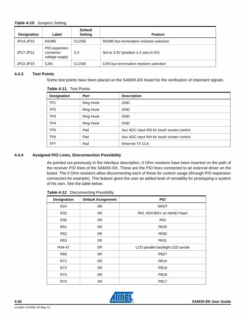
4.4.3 Test Points
Some test points have been placed on the SAM3X-EK board for the verification of important signals.
4.4.4 Assigned PIO Lines, Disconnection Possibility
As pointed out previously in the interface description, 0 Ohm resistors have been inserted on the path of the receiver PIO lines of the SAM3X-EK. These are the PIO lines connected to an external driver on the board. The 0 Ohm resistors allow disconnecting each of these for custom usage (through PIO expansion connectors for example). This feature gives the user an added level of versatility for prototyping a system of his own. See the table below.
JP14-JP16 RS485 CLOSE RS485 bus termination resistors selection
JP17-JP21PIO expansion connector voltage supply
2-3 Set to 3.3V (position 1-2 sets to 5V)
JP22-JP23 CAN CLOSE CAN bus termination resistors selection
Table 4-10. Jumpers Setting
Designation LabelDefault Setting Feature
Table 4-11. Test Points
Designation Part Description
TP1 Ring Hook GND
TP2 Ring Hook GND
TP3 Ring Hook GND
TP4 Ring Hook GND
TP5 Pad Aux ADC input IN3 for touch screen control
TP6 Pad Aux ADC input IN4 for touch screen control
TP7 Pad Ethernet TX CLK
Table 4-12. Disconnecting Possibility
Designation Default Assignment PIO
R24 0R NRST
R32 0R PA2, RDY/BSY on NAND Flash
R35 0R PA3
R51 0R PA28
R52 0R PA30
R53 0R PA31
R44-47 0R LCD parallel backlight LED anode
R60 0R PB27
R71 0R PA14
R72 0R PB19
R73 0R PB18
R74 0R PB17
4-26 SAM3X-EK User Guide
11156A–ATARM–25-May-12
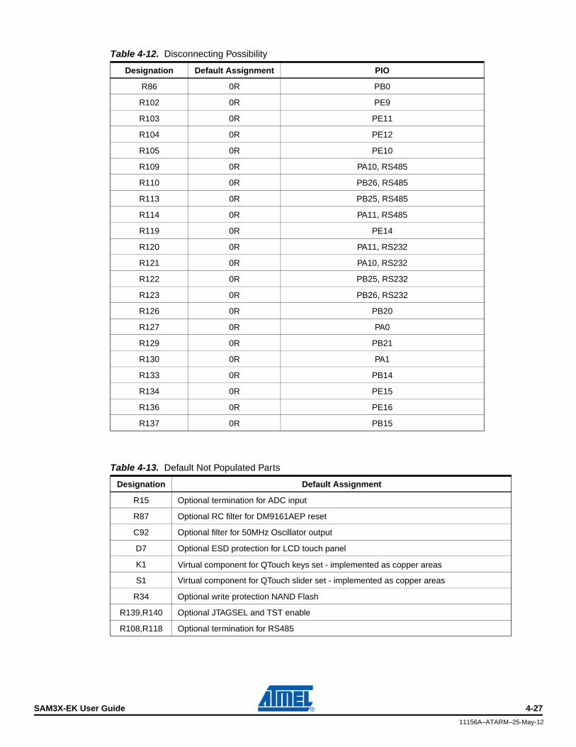
R86 0R PB0
R102 0R PE9
R103 0R PE11
R104 0R PE12
R105 0R PE10
R109 0R PA10, RS485
R110 0R PB26, RS485
R113 0R PB25, RS485
R114 0R PA11, RS485
R119 0R PE14
R120 0R PA11, RS232
R121 0R PA10, RS232
R122 0R PB25, RS232
R123 0R PB26, RS232
R126 0R PB20
R127 0R PA0
R129 0R PB21
R130 0R PA1
R133 0R PB14
R134 0R PE15
R136 0R PE16
R137 0R PB15
Table 4-13. Default Not Populated Parts
Designation Default Assignment
R15 Optional termination for ADC input
R87 Optional RC filter for DM9161AEP reset
C92 Optional filter for 50MHz Oscillator output
D7 Optional ESD protection for LCD touch panel
K1 Virtual component for QTouch keys set - implemented as copper areas
S1 Virtual component for QTouch slider set - implemented as copper areas
R34 Optional write protection NAND Flash
R139,R140 Optional JTAGSEL and TST enable
R108,R118 Optional termination for RS485
Table 4-12. Disconnecting Possibility
Designation Default Assignment PIO
SAM3X-EK User Guide 4-27
11156A–ATARM–25-May-12
Section 5
Schematics
5.1 SchematicsThis section contains the following schematics:
TOP LEVEL
POWER SUPPLY & USB & JTAG
ATSAM3X_LFBGA217
EBI_MEMORY
DISPLAY & QTouch
Audio & HSMCI & TWI
ETHERNET & ZIGBEE
SERIAL & USER INTERFACES
SAM3X-EK User Guide 5-1
11156A–ATARM–25-May-12
5
5
4
4
3
3
2
2
1
1
D D
C C
B B
A A
USE
R'S
INTE
RFA
CE
CARDREADER
ATMELCortex-M3 ARM Processor SAM3X (LFBGA217)
EBI SDRAM INTERFACE
EBI NANDFLASH INTERFACE
POWER SUPPLY
MM
C S
DSD
IO
PIO
A1A2A3A4
PIO
PIO
USAGE
PB0PB1
PB2PB3PB4PB5PB6PB7PB8PB9PB10PB11PB12PB13PB14PB15
USAGE
PB16PB17PB18
PB19PB20PB21PB22PB23PB24PB25PB26PB27PB28PB29PB30PB31
SPI0_MISOSPI0_MOSISPI0_SPCKSPI0_NPCS0
USAGEPA0PA1PA2PA3PA4PA5PA6PA7PA8PA9PA10PA11PA12PA13PA14PA15
USAGE
PA16
PA17PA18PA19PA20PA21PA22PA23PA24PA25PA26PA27PA28PA29
5 V
PA30PA31
MCCKMCCDAMCDA0
MCDA2MCDA1
MCDA3
MCDA4MCDA5MCDA6MCDA7
PIO MUXINGUSAGE
PE0PE1PE2PE3PE4PE5PE6PE7PE8PE9
PE10PE11PE12PE13PE14PE15
USAGE
PE16PE17PE18PE19PE20PE21PE22PE23PE24PE25PE26
PE27PE28PE29PE30PE31
3V3REWOP
USAGE
PD0PD1PD2PD3PD4PD5PD6
PD7PD8PD9PD10PD11PD12PD13PD14PD15
USAGE
PD16PD17PD18PD19PD20PD21PD22PD23
PD24PD25PD26PD27PD28PD29PD30
USAGE
PC0PC1PC2PC3
PC4PC5PC6PC7PC8PC9PC10PC11PC12PC13PC14PC15
USAGE
PC16PC17PC18PC19PC20
PC21PC22PC23PC24PC25PC26PC27PC28PC29PC30
NANDALENANDCLENANDRDY
PIO A,...F
PIO A,...F
USB
Sheet 2
Sheet 3
Sheet 6
Sheet 5
EBI
"DNP" means the component is not populated by defaultNOTE
HE 1
0 ICEINTERFACE
SDRA
M25
6Mbi
t
HOSTDEVICE
LCD INTERFACE2.8"240x320TFT
TOUCH SCREEN
SERIALEEPROM
AUDIO
NAND
FLAS
H
PF0PF1PF2PF3PF4PF5
TWD0TWCK0
PCK0
TKTFTD
RFRD
RK
NCS2
NWE
NRD
D0D1
D2D3D4D5D6D7D8D9D10D11D12D13D14D15
SDA10
A13
A14
SDCKE
NBS1
NBS0
SDWE
CASRAS
NCS1
NANDOENANDWE
NCS0MDINTR
AD1
TCKTDITDOTMS
UOTGVBOFUOTGID
EREFCKETXEN
ETX0ETX1ECRSDVERX0ERX1ERXEREMDCEMDIO
URXDUTXDRXD0TXD0
RTS0CTS0
COM0_EN
CANTX0CANRX0
CANTX1CANRX1
CANTX0RSCANRX0EN
SPI1_MISOSPI1_MOSISPI1_SPCKSPI1_NPCS0QTSLIDR_SL_SNSQTSLIDR_SL_SNSKQTSLIDR_SM_SNSQTSLIDR_SM_SNSKQTSLIDR_SR_SNSQTSLIDR_SR_SNSK
ZB_RSTN
ZB_SLPTR
USB_FAULT
ZB_IRQ0ZB_IRQ1
ERASE
BP4_RIGHT
BP5_LEFT
QTOUCH
MIC
OU
T
POT
ADC1
IRQ_TSCBUSY_TSC MCI_CDPOWER_LED
USER_LED3USER_LED1USER_LED2
BL_EN
A5A6A7A8A9
BA0
BA1
A10A11
CANTX1RSCANRX1EN
QTVALID_SNSQTVALID_SNSKQTUP_SNSQTUP_SNSKQTDOWN_SNSQTDOWN_SNSKQTLEFT_SNSQTLEFT_SNSKQTRIGHT_SNS
QTRIGHT_SNSK
SDCS
UART
COM RS23
2
Sheet 4
Sheet 8
HE 1
0RJ
12CAN0
CAN1
RS48
5
USART0
PIOEXPANSIONCONNECTOR
10/100 FAST ETHERNET
Sheet 7
RJ 4
5HE
10 ZIGBEE
INTERFACE
OSC_OE
REV DATEMODIF. DES. DATE VER.SCALE 1/1 REV. SHEET
This agreement is our property. Reproduction and publication without our written authorization shall expose offender to legal proceedings.
18A
XX-XXX-XXWL XXX
TOP LEVEL
2010-03-12
SAM3X-EK
INIT EDITA61-80-0102B WL
REV DATEMODIF. DES. DATE VER.SCALE 1/1 REV. SHEET
This agreement is our property. Reproduction and publication without our written authorization shall expose offender to legal proceedings.
18A
XX-XXX-XXWL XXX
TOP LEVEL
2010-03-12
SAM3X-EK
INIT EDITA61-80-0102B WL
REV DATEMODIF. DES. DATE VER.SCALE 1/1 REV. SHEET
This agreement is our property. Reproduction and publication without our written authorization shall expose offender to legal proceedings.
18A
XX-XXX-XXWL XXX
TOP LEVEL
2010-03-12
SAM3X-EK
INIT EDITA61-80-0102B WL
5
5
4
4
3
3
2
2
1
1
D D
C C
B B
A A
AD1
USR_LED1#
USR_LED2#
POWER_LED#
USB
ICE INTERFACE
USR_LED3#
Potentiometer
(UOTGVBOF)
(UOTGID)
BUTTONS
NRST
NRSTB
WAKE UP
RIGHT CLICK
LEFT CLICK
USB_FAULT
Vout=(Rup/Rdown+1)*1.24
ADHESIVE FEET
PWR_CN
+5V
+5V
+5V
+5V
+3V3
+3V3
+3V3
+3V3
+3V3
+3V3
+3V3
SHDN[3]
PB30[3,8]
PB28[3,8]PB31[3,8]PB29[3,8]
NRST[3,5,7]
PA13 [3,8]
PB12 [3,8]
VDDANA [3]
VDDUTMI [3]
VDDIN [3]
VDDIO [3]
VDDCORE [3]
VDDPLL [3]
VDDOUT[3]
VDDBU[3]
PE5 [3,8]
PB10 [3,8]
DHSDM [3]DHSDP [3]PB11 [3,8]
PA3 [3,8]
PA12 [3,8]
PB13 [3,8]
NRST [3,5,7]
NRSTB [3]
FWUP [3]
PB23 [3,8]
PE7 [3,8]
VDDBU [3]
VBUS [3]
VDDBU [3]
REV DATEMODIF. DES. DATE VER.SCALE 1/1 REV. SHEET
This agreement is our property. Reproduction and publication without our written authorization shall expose offender to legal proceedings.
29A
XX-XXX-XXWL XXX
POWER SUPPLY & USB & JTAG
2010-03-12
SAM3X-EK
INIT EDITA2010-08-16WLB
REV DATEMODIF. DES. DATE VER.SCALE 1/1 REV. SHEET
This agreement is our property. Reproduction and publication without our written authorization shall expose offender to legal proceedings.
29A
XX-XXX-XXWL XXX
POWER SUPPLY & USB & JTAG
2010-03-12
SAM3X-EK
INIT EDITA2010-08-16WLB
REV DATEMODIF. DES. DATE VER.SCALE 1/1 REV. SHEET
This agreement is our property. Reproduction and publication without our written authorization shall expose offender to legal proceedings.
29A
XX-XXX-XXWL XXX
POWER SUPPLY & USB & JTAG
2010-03-12
SAM3X-EK
INIT EDITA2010-08-16WLB
JP2JP2
B1
BN03K314S300R
B1
BN03K314S300R
R2
1R
R2
1R
Z5
11.1
Z5
11.1
R11470RR11470R
R5100KR5100K
VBUS
SHD DM
DPID
GND
J3
USB Micro AB
VBUS
SHD DM
DPID
GND
J3
USB Micro AB
12345
7
6
C8100nFC8
100nF
R12
1K
R12
1K
R15DNPR15DNP
R16
1R
R16
1R
C24100nFC24100nF
Z3
11.1
Z3
11.1
R13
1K
R13
1K
L110uH/150mAL110uH/150mA
BP2BP21
423
RV1
V5.5MLA0603
RV1
V5.5MLA0603
C154.7uFC154.7uF
C4
100nF
C4
100nF
J2J2
VTref1
Vsupply2
nTRST3
GND14
TDI5
GND26
TMS7
GND38
TCK9
GND410
RTCK11
GND512
TDO13
GND614
nSRST15
GND716
DBGRQ17
GND818
DBGACK19
GND920
C17100nFC17100nF
TP4GNDTP4GND
C124.7uFC124.7uF
+ C10100uF
+ C10100uF
BP3BP31
423
R21100KR21100K
D1BAT54CD1BAT54C
32
1
C22 10nFC22 10nF
C7
100nF
C7
100nF
Q3IRLML2502
Q3IRLML2502
1
3
2
R19100KR19100K
C144.7uFC144.7uF
JP3JP3Q2
IRLML2502Q2
IRLML25021
3
2
J1MP179P 2.1mm
J1MP179P 2.1mm
12
3
JP1-1JP1-11 2
R22100KR22100K
L310uH/150mAL310uH/150mA
JP1-5JP1-59 10
Z6
11.1
Z6
11.1
MN4
SP2525-2
MN4
SP2525-2
EN1
FLG2
NC14
OUT28
OUT16
IN7
NC25
GND3
R23 100KR23 100K
R8
10K
R8
10K
TP2GNDTP2GND
R20100KR20100K
C2010nFC2010nF
MN1ZEN056V130A24LSMN1ZEN056V130A24LS
1
2
3
C18100nFC18
100nF
D4
green
D4
green
JP1-4JP1-47 8
R10470RR10470R
JP1-2JP1-23 4
C3100nFC3
100nF
C1100nFC1100nF
BP4BP41
423
MN2BNX002-01MN2BNX002-01
SV1
SG2
CV3
CG14
CG25
CG36
D5
red
D5
red
R3169K 1%R3169K 1%
L210uH/150mAL210uH/150mA
C21100nFC21
100nF
D2
Blue
D2
Blue
C11100nFC11100nF
R14100KR14100K
JP1-3JP1-35 6
VR110KVR110K
13
24
5
R6102K 1%R6102K 1%
JP1-6JP1-611 12
C194.7uFC194.7uF
C6100nFC6
100nF
BP5BP51
423
R35 0RR35 0R
D3
Amber
D3
Amber
TP3GNDTP3GND
R18100KR18100K
Q1IRLML6401Q1IRLML6401
132
+ C222uF
+ C222uF
Z4
11.1
Z4
11.1
C54.7uFC54.7uF
BT1CR12_16_20_25BT1CR12_16_20_25
TP1GNDTP1GND
C1315pFC1315pF
R24 0RR24 0R
Z1
11.1
Z1
11.1
R1
1R
R1
1R
BP1BP11
423
R17
100K
R17
100K
MN3MIC29152WUMicrel's 1.5A LDO, TO263-5
MN3MIC29152WUMicrel's 1.5A LDO, TO263-5
VIN2
VOUT4
SD1
GN
D1
3
ADJ5
GN
D2
6
JP4
JP
JP4
JP
R710KR710K
C94.7uFC94.7uF
R4100KR4100K
Z2
11.1
Z2
11.1
+ C2333uF
+ C2333uF
5
5
4
4
3
3
2
2
1
1
D D
C C
B B
A A
(ERASE)
+3V3
+3V
PA0PA1PA2PA3PA4PA5PA6PA7PA8PA9PA10PA11PA12PA13PA14PA15PA16PA17PA18PA19PA20PA21PA22PA23PA24PA25PA26PA27PA28PA29PA30PA31
PB0PB1PB2PB3PB4PB5PB6PB7PB8PB9PB10PB11PB12PB13PB14PB15PB16PB17PB18PB19PB20PB21PB22PB23PB24PB25PB26PB27PB28PB29PB30PB31
PC0PC1PC2PC3PC4PC5PC6PC7PC8PC9PC10PC11PC12PC13PC14PC15PC16PC17PC18PC19PC20PC21PC22PC23PC24PC25PC26PC27PC28PC29PC30
PE0PE1PE2PE3PE4PE5PE6PE7PE8PE9PE10PE11PE12PE13PE14PE15PE16PE17PE18PE19PE20PE21PE22PE23PE24PE25PE26PE27PE28PE29PE30PE31
PF0
PF2PF3
PF1
PF4PF5
VBG
JTAGSEL
TST
TST
VBG
JTAGSEL
PD8
PD5
PD24
PD0
PD3
PD28
PD7
PD1
PD20
PD2
PD14
PD27
PD6
PD25
PD23
PD18
PD12
PD10
PD19
PD17
PD13
PD29
PD26
PD4
PD21PD22
PD16
PD11
PD9
PD15
PD30
PD11
PD28
PD30
PD21
PD15
PD7
PD14
PD19
PD1
PD10
PD2
PD5
PD13
PD27
PD22
PD18
PD0
PD9
PD24
PD16
PD8
PD4
PD12
PD29
PD26
PD20
PD25
PD23
PD6
PD17
PD3
+3V3 +5V
PA[0..31] [2,4,5,6,7,8] PB[0..31][2,5,6,7,8] PC[0..30] [4,5,8] PD[0..30][4,6,7,8] PE[0..31] [2,5,6,7,8] PF[0..5][5]
DHSDP[2]DHSDM[2]
PC0 [8]
VDDCORE [2]
VDDIN [2]
VDDOUT [2]
VDDBU[2]
FWUP[2]
SHDN[2]
NRSTB[2]
NRST[2,5,7]
VBUS[2]
VDDIO[2]
VDDIO [2]
VDDUTMI [2]
VDDBU [2]
VDDPLL [2]
VDDANA [2]
SDCK [4]
REV DATEMODIF. DES. DATE VER.SCALE 1/1 REV. SHEET
This agreement is our property. Reproduction and publication without our written authorization shall expose offender to legal proceedings.
38A
XX-XXX-XXWL XXX
ATSAM3X_LFBGA217
2010-03-12
SAM3X-EK
INIT EDITA2010-08-16WLB
REV DATEMODIF. DES. DATE VER.SCALE 1/1 REV. SHEET
This agreement is our property. Reproduction and publication without our written authorization shall expose offender to legal proceedings.
38A
XX-XXX-XXWL XXX
ATSAM3X_LFBGA217
2010-03-12
SAM3X-EK
INIT EDITA2010-08-16WLB
REV DATEMODIF. DES. DATE VER.SCALE 1/1 REV. SHEET
This agreement is our property. Reproduction and publication without our written authorization shall expose offender to legal proceedings.
38A
XX-XXX-XXWL XXX
ATSAM3X_LFBGA217
2010-03-12
SAM3X-EK
INIT EDITA2010-08-16WLB
C26 100nFC26 100nF
R29
0RR
290R
R274.7KR274.7K
C41 100nFC41 100nF
R140 DNPR140 DNP
C28 100nFC28 100nF
MN5GATSAM3X_LFBGA217MN5GATSAM3X_LFBGA217
VBGU3
VBUSU4
DHSDMT2
VDDCORED10
VDDIOD9
VDDCOREG14
GN
DP
LLN
2
VDDPLLN1
XOUTP2
XINP1
DHSDPT1
NC
3P
5
DFSDPU1
DFSDMU2
GN
DU
TMI
R2
VDDCOREJ4
JTAGSELT4NRSTB
R5
XIN32U5
ADVREFU15
VDDCOREL4
VDDIOH4
GN
DA
NA
U14
VDDINU8
VDDOUTU7
FWUPT6
NC
5N
3
TSTR6
SHDNT5
XOUT32U6
VDDANAT14
NRSTP15
NC
4P
6
VDDIOH9
VDDIOH14
SDCKD11
VDDCOREP10
VDDIOP11
GN
DH
8
GN
DH
10
GN
DJ8
GN
DJ9
GN
DJ1
0
GN
DK
8
VDDCORER1
NC
6R
4
VDDBUP8
GN
DB
UP
7
VDDTUMIT3
GN
DK
9
GN
DK
10
NC
1P
3
NC
2R
3
C162.2uFC162.2uF
R25 39RR25 39R
C4810pFC4810pF
JP7JP7
1
2
3
MN5C
ATSAM3X_LFBGA217
MN5C
ATSAM3X_LFBGA217
PC2T7
PC3R8
PC7R13
PC8T13
PC9U13
PC11M15
PC12L14
PC13L15
PC14K15
PC5N14
PC6P14
PC10B14
PC4C14
PC15K14
PC16J14
PC17J17
PC18J16
PC19J15
PC29H17
PC30H16
PC0C8
PC20C7
PC21A6
PC22D7
PC23B6
PC24C6
PC25A5
PC26B5
PC27C5
PC28A4
PC1R7
C29 100nFC29 100nF
MN5E
ATSAM3X_LFBGA217
MN5E
ATSAM3X_LFBGA217
PE30H1 PE29H3 PE28G1 PE27G2 PE26G3
PE24A2 PE23D6 PE22D5 PE21D4
PE0E17
PE1F14
PE2E16
PE3E15
PE4D17
PE5D16
PE6E14
PE7D15
PE8C17
PE9A12
PE10C11
PE11B11
PE12A11
PE13C10
PE14B10
PE15A10
PE16B8
PE17A8
PE18A7
PE25B12
PE31F15
PE19B7
PE20D8
C33 10pFC33 10pF
C40 20pFC40 20pF
SUP1
SG-BGA-6004
SUP1
SG-BGA-6004
C34 100nFC34 100nF
R139 DNPR139 DNP
MN5A
ATSAM3X_LFBGA217
MN5A
ATSAM3X_LFBGA217
PA9B2
PA10B1
PA11C2
PA12C1
PA13D3
PA14D2
PA15D1
PA17E4
PA0J1
PA1J3
PA5K3
PA7K2
PA8K1
PA2N16
PA3P17
PA4P16
PA6R17
PA16U16
PA18R14
PA19M14
PA20R15
PA22R16
PA23T17
PA24U17
PA30T10
PA31T8
PA21C16
PA25B17
PA26A17
PA27B16
PA28A16
PA29C15
C35 100nFC35 100nF
C39 100nFC39 100nF
C25 100nFC25 100nF
C43 100nFC43 100nF
C47100nFC47100nF
C27 100nFC27 100nF
C38 100nFC38 100nF
R26 39RR26 39R
MN5F
ATSAM3X_LFBGA217
MN5F
ATSAM3X_LFBGA217
PF1L2
PF2M1
PF3M2
PF4M3
PF5M4
PF0D12
C36 10pFC36 10pF
Y232.768KHz
Y232.768KHz
123 4
R286.8K 1%R286.8K 1%
Y112MHz
Y112MHz
123 4
C30 100nFC30 100nF
C45 100nFC45 100nF
C42 20pFC42 20pF
MN5B
ATSAM3X_LFBGA217
MN5B
ATSAM3X_LFBGA217
PB26A1
PB28K4
PB29L1
PB30L3
PB31N4
PB27N15
PB16T16PB15T15
PB12N17
PB13M16
PB17M17
PB18L16
PB19L17
PB20K17
PB21K16
PB0B15
PB1A15
PB2D14
PB3A14
PB4C13
PB5D13
PB6B13
PB7A13
PB8C12
PB9B9
PB10A9
PB11C9
PB14B4
PB22C4
PB23A3
PB24B3
PB25C3
C49100nFC49100nF
C37 100nFC37 100nF
JP6JP6 D6
LM4040-3.0
D6
LM4040-3.0
MN5D
ATSAM3X_LFBGA217
MN5D
ATSAM3X_LFBGA217
PD10P4PD9J2PD8H2PD7G4PD6F1PD5F2PD4F3PD3F4PD2E1PD1E2PD0E3
PD11P9
PD12R9
PD13T9
PD14U9
PD15U10
PD16R10
PD17R11
PD18T11
PD19U11
PD20P12
PD21P13
PD22R12
PD23T12
PD24U12
PD25H15
PD26G17
PD27G16
PD28G15
PD29F17
PD30F16
5
5
4
4
3
3
2
2
1
1
D D
C C
B B
A A
(NCS0)
(NANDRDY)
(NANDALE)(NANDCLE)
Optional 16bits DATA BUSWith MT29F2G16AAD Micron
256 Mbits SDRAM
(NANDWE)(NANDOE)
(SDA10)
(A2)(A3)(A4)(A5)(A6)(A7)(A8)(A9)(A10)(A11)
(A13)
(A14)
(BA0)(BA1)
(SDCKE)
(NBS0)(NBS1)
CASRAS
(SDWE)
(SDCS)
8-bits NAND Flash is mounted by default
PC8
PC2
PC5PC6
PC4PC3
PC7
PC9
PC16
PC10
PC13PC14
PC12PC11
PC15
PC17
PD6PD7
PD4
PC2PC3PC4PC5PC6PC7
PD16
PC8
PD13
PD10
PD15
PC9
PD14
PC10PD22PD23
PC29
PC27
PC30
PC26
PC28
PC11PC12PC13PC14PC15
PD25
PC16PC17
PD11
PC23PC24PC25
+3V3
+3V3
+3V3
+3V3
PC[0..30][3,5,8]
PD9[3,8]PD8[3,8]PC19[3,8]PC20[3,8]PA6[3,8]
PA2[3,8]
SDCK[3]
PC21[3,8]
PC[0..30][3,5,8]
PD[0..30][3,6,7,8]
PD12[3,8]
REV DATEMODIF. DES. DATE VER.SCALE 1/1 REV. SHEET
This agreement is our property. Reproduction and publication without our written authorization shall expose offender to legal proceedings.
48A
XX-XXX-XXWL XXX
EBI_MEMORY
2010-03-12
SAM3X-EK
INIT EDITA2010-08-16WLB
REV DATEMODIF. DES. DATE VER.SCALE 1/1 REV. SHEET
This agreement is our property. Reproduction and publication without our written authorization shall expose offender to legal proceedings.
48A
XX-XXX-XXWL XXX
EBI_MEMORY
2010-03-12
SAM3X-EK
INIT EDITA2010-08-16WLB
REV DATEMODIF. DES. DATE VER.SCALE 1/1 REV. SHEET
This agreement is our property. Reproduction and publication without our written authorization shall expose offender to legal proceedings.
48A
XX-XXX-XXWL XXX
EBI_MEMORY
2010-03-12
SAM3X-EK
INIT EDITA2010-08-16WLB
C58
100n
FC
5810
0nF
R31
470K
R31
470K
C52
100n
FC
5210
0nF
C57
100n
FC
5710
0nF
C55
100n
FC
5510
0nF
C51100nFC51100nF
MT48LC16M16A2
MN7
MT48LC16M16A2
MN7
A023
A124
A225
A326
A429
A530
A631
A732
A833
A934
A1022
BA020
A1236
DQ02
DQ14
DQ25
DQ37
DQ48
DQ510
DQ611
DQ713
DQ842
DQ944
DQ1045
DQ1147
DQ1248
DQ1350
DQ1451
DQ1553
VDD1
VSS28
VSS41
VDDQ3VDD27
N.C40
CLK38
CKE37
DQML15
DQMH39
CAS17
RAS18
WE16
CS19
VDDQ9
VDDQ43
VDDQ49
VSSQ6
VSSQ12
VSSQ46
VSSQ52
VDD14
VSS54
A1135
BA121
C56
100n
FC
5610
0nF
C54
100n
FC
5410
0nF
C53
100n
FC
5310
0nF
R33 470KR33 470K
R34
DNP
R34
DNP
C50100nFC50100nF
R32 0RR32 0R
JP8JP8
MN8
MT29F2G08AAD
MN8
MT29F2G08AAD
WE18
N.C66
VCC37
CE9
RE8
N.C1120
WP19
N.C55
N.C11
N.C22
N.C33
N.C44
DNU121
DNU222
N.C1223
N.C1324
R/B7
I/O8_N.C26
I/O9_N.C27
I/O10_N.C28
I/O029
VCC_N.C34
N.C1435
VSS36
DNU338
VCC_N.C39
VCC12
VSS13
ALE17
N.C811 N.C710
N.C914
N.C1015
CLE16
VSS_N.C25
I/O11_N.C33
I/O130
I/O332I/O231
I/O15_N.C47I/O14_N.C46I/O13_N.C45
I/O744I/O643I/O542I/O441
I/O12_N.C40
VSS_N.C48
JP9JP9
R30
1K
R30
1K
5
5
4
4
3
3
2
2
1
1
D D
C C
B B
A A
The part is placed as close as possible to J4
NOT POPULATED
QST Keys
LCD TOUCH SCREEN
(NCS2)A1NWENRD
(SPI0_MOSI)(SPI0_SPCK)
(SPI0_MISO)(SPI0_NPCS0)
IRQ_TSCBUSY_TSC
2.8" 320x240 TFT LCD DISPLAY
QT Slider
X_RIGHT
X_LEFTY_UP
Y_DOWN
X_RIGHTY_UPX_LEFTY_DOWN
PC22PC18
PC3PC2
PC4
PC6PC5
PC8PC9
PC7
PC16
PC10
PC13PC14
PC11
PC15
PC12
PC17
X_RIGHT
X_LEFTY_DOWN
Y_UP
LED_A1LED_A2LED_A3LED_A4
LED_A1LED_A2LED_A3LED_A4
+3V3
+3V3
+3V3
+3V3 +3V3
+3V3
AGND_TPAGND_TP
+3V3
NRST[2,3,7]
PC[0..30][3,4,8]
PB24[3,8]
PA29[3,8]
PB27[3,8]
PA27 [3,8]PA26 [3,8]
PA28 [3,8]PA25 [3,8]
PA30 [3,8]PA31 [3,8]
PF0[3]
PF1[3]
PF2[3]
PF3[3]
PF4[3]
PF5[3]
PE20[3]
PE21[3]
PE26[3]
PE27[3]
PE24[3]
PE25[3]
PE18[3]
PE19[3]
PE22[3]
PE23[3]
REV DATEMODIF. DES. DATE VER.SCALE 1/1 REV. SHEET
This agreement is our property. Reproduction and publication without our written authorization shall expose offender to legal proceedings.
58A
XX-XXX-XXWL XXX
DISPLAY & QTouch
2010-03-12
SAM3X-EK
INIT EDITA2010-08-16WLB
REV DATEMODIF. DES. DATE VER.SCALE 1/1 REV. SHEET
This agreement is our property. Reproduction and publication without our written authorization shall expose offender to legal proceedings.
58A
XX-XXX-XXWL XXX
DISPLAY & QTouch
2010-03-12
SAM3X-EK
INIT EDITA2010-08-16WLB
REV DATEMODIF. DES. DATE VER.SCALE 1/1 REV. SHEET
This agreement is our property. Reproduction and publication without our written authorization shall expose offender to legal proceedings.
58A
XX-XXX-XXWL XXX
DISPLAY & QTouch
2010-03-12
SAM3X-EK
INIT EDITA2010-08-16WLB
R39 1KR39 1K
C731uFC731uF
R41 1KR41 1K
R52 0RR52 0R
C761uFC761uF
R53 0RR53 0R
PINs
onBO
T
PIN 39
PIN 1
FTM280C12D
PINs
onBO
T
PIN 39
PIN 1
FTM280C12D+ C6610uF
+ C6610uF
B2BN03K314S300RB2BN03K314S300R
R590RR590R
C6222nFC6222nF
R49100KR49100K
R54 0RR54 0R
C754.7uFC754.7uF
J4FH26-39S-0.3SHWJ4FH26-39S-0.3SHW
GND11
CS2
RS3
WR4
RD5
DB06
DB17
DB28
DB39
DB410
DB511
DB612
DB713
DB814
DB915
DB1016
DB1117
DB1218
DB1319
DB1420
DB1521
NC122
NC223
RESET24
GND225
X+26
Y+27
X-28
Y-29
GND330
VDD131
VDD232
A133
A234
A335
A436
NC337
NC438
K39
C6322nFC6322nF
C69100nFC69100nF
R51 0RR51 0R
R57100KR57100K
C6522nFC6522nF
C744.7uFC744.7uF
L410uH/150mAL410uH/150mA
C6122nFC6122nF
C6822nFC6822nF
C70100nFC70100nF
R36100KR36100K
R58100KR58100K
R5647KR5647K
R44 0RR44 0R
R42 1KR42 1K
C5922nFC5922nF
C71100nFC71100nF
R48 1KR48 1K
R45 0RR45 0R
R600RR600R
TP6SMDTP6SMD
K1DNPK1DNP
R551RR551R
R46 0RR46 0R
R40 1KR40 1K
S1DNPS1DNP
SL
SM
SR
SR
R43 1KR43 1K
R47 0RR47 0R
MN10AAT3194ITPMN10AAT3194ITP
C1+4
C1-3
EN/SET9
C2+1
C2-12
OUT2
IN10
GND11
D18
D27
D36
D45
C6022nFC6022nF
MN9ADS7843EMN9ADS7843E
XP2
YP3
XM4
YM5
DCLK16
DIN14
DOUT12
CS15
BUSY13
PENIRQ11
VREF9
VCC11
VCC210
GND6
IN37
IN48
D7DNPTVS, SOT23-5
D7DNPTVS, SOT23-5
1
2
345
R38 1KR38 1K
C6422nFC6422nF
TP5SMDTP5SMD
JP10JP10
R37 1KR37 1K
R50100KR50100K
C67100nFC67100nF
C721uFC721uF
5
5
4
4
3
3
2
2
1
1
D D
C C
B B
A A
HEADPHONELINE-OUT
MONO MICRO INPUT
SERIAL EEPROM
(TWCK0)(TWD0)
(TWD0)(TWCK0)(PCK0)
(TD)(TF)(RD)(RF)
(TK)(RF)
(MCCK)(MCDA6)
(MCCDA)
(MCDA2)
(MCDA3)(MCDA4)
(MCDA5)
(MCDA7)
(MCDA0)(MCDA1)
(MCI_CD)
+3V3
+3V3 +3V3 +3V3
+3V3
+3V3
+3V3
+3V3
+3V3
AVDD
AVDD
AGND_AUDIO
AGND_AUDIOAGND_AUDIO
AGND_AUDIO
AGND_AUDIO
AGND_AUDIO
AGND_AUDIO
AGND_AUDIO
PA18[3,8]PA17[3,8]
PA18[3,8]PB22[3,8]PA14[3,8]
PA15[3,8]PA16[3,8]
PD0[3,8]PA24[3,8]
PD1[3,8]PA20[3,8]
PA23[3,8]
PD3[3,8]
PA22[3,8]PA21[3,8]
PD2[3,8]PA19[3,8]
PA17[3,8]
PB19[3,8]
PB18[3,8]PB17[3,8]
PE6[3,8]
REV DATEMODIF. DES. DATE VER.SCALE 1/1 REV. SHEET
This agreement is our property. Reproduction and publication without our written authorization shall expose offender to legal proceedings.
68A
XX-XXX-XXWL XXX
Audio & HSMCI & TWI
2010-03-12
SAM3X-EK
INIT EDITA2010-08-16B WL
REV DATEMODIF. DES. DATE VER.SCALE 1/1 REV. SHEET
This agreement is our property. Reproduction and publication without our written authorization shall expose offender to legal proceedings.
68A
XX-XXX-XXWL XXX
Audio & HSMCI & TWI
2010-03-12
SAM3X-EK
INIT EDITA2010-08-16B WL
REV DATEMODIF. DES. DATE VER.SCALE 1/1 REV. SHEET
This agreement is our property. Reproduction and publication without our written authorization shall expose offender to legal proceedings.
68A
XX-XXX-XXWL XXX
Audio & HSMCI & TWI
2010-03-12
SAM3X-EK
INIT EDITA2010-08-16B WL
R644.7KR644.7K
C81100nFC81100nF
B3BN03K314S600RB3BN03K314S600R
R6247KR6247K
R78 0RR78 0R
R8010KR8010K
R77 330RR77 330R
R83
10K
R83
10KR8110KR8110K
R664.7KR664.7K
J7PHONEJACKJ7PHONEJACK
54321
+ C8210uF
+ C8210uF
MN11XWM8731EDSMN11XWM8731EDS
DBVDD1
CLKOUT2
BCLK3
DACDAT4
DACLRC5
ADCDAT6
ADCLRC7
HPVDD8
LHPOUT9
RHPOUT10
HPGND11
LOUT12
ROUT13
AVDD14
AGND15
VMID16
MICBIAS17
MICIN18
RLINEIN19
LLINEIN20
MODE21
CSB22
SDIN23
SCLK24
XTI/MCLK25
XTO26
DCVDD27
DGND28
C88470pFC88470pF
RR147KX4RR147KX4
12345 6 7 8
C100100nFC100100nF
R8210KR8210K
R75 680RR75 680R
R67 100KR67 100K
J87SDMM-B0-2211-AJ87SDMM-B0-2211-A
DAT21
RSV/DAT32
DAT43
CMD4
DAT55
GND6
VCC7
CLK8
DAT69
CD10
DAT711
DAT012
DAT113
SD_WP14
GROUND115
GROUND16
SHELLED117
SHELLED218
R7947KR7947K
C78100nFC78100nF
+ C7710uF
+ C7710uF
B4BN03K314S600RB4BN03K314S600R
R63100KR63100K
R68 100KR68 100K
B7BN03K314S600RB7BN03K314S600R
RR247KX4RR247KX4
12345 6 7 8
R74 0RR74 0R
+C86 220uF+C86 220uF
C87470pFC87470pF
R6147KR6147K
J5PHONEJACKJ5PHONEJACK
54321
C102100nFC102100nF
MN12
AT24C512BN
MN12
AT24C512BN
A01
A12
WP7
SCL6
VCC8 A3
3SDA5
GND4
R650RR650R
+ C9147uF
+ C9147uF
+ C8410uF
+ C8410uF
+ C10110uF
+ C10110uF
R73 0RR73 0R
C80100nFC80100nF
+C83 220uF+C83 220uF
L510uH/150mAL510uH/150mA
C79100nFC79100nF
R71 0RR71 0R
C98 1uFC98 1uF
JP11JP11
C85100nFC85100nF
R72 0RR72 0R
C99220pFC99220pF
C90100nFC90100nF
R76 10KR76 10K
+ C8910uF
+ C8910uF
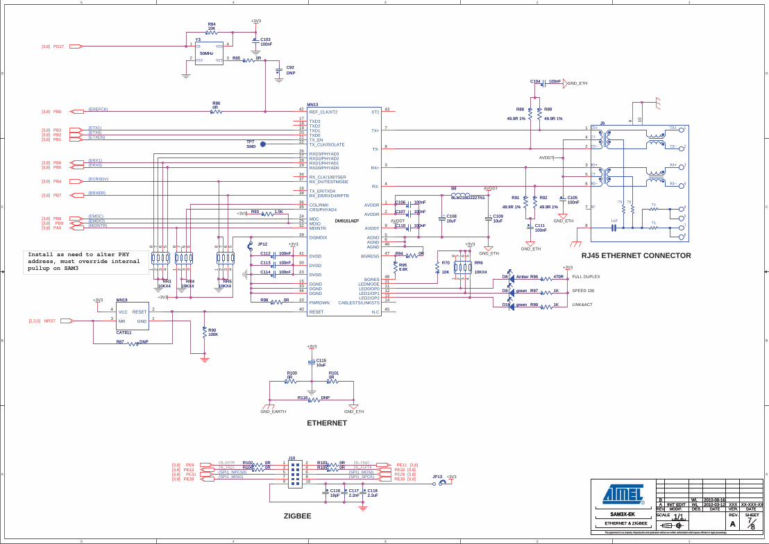
5
5
4
4
3
3
2
2
1
1
D D
C C
B B
A A
(ERX1)(ERX0)
RJ45 ETHERNET CONNECTOR
(ETX1)(ETX0)(ETXEN)
(EMDC)(EMDIO)(MDINTR)
(ERXER)
SPEED 100
FULL DUPLEX
LINK&ACT
(EREFCK)
ZIGBEE
Install as need to alter PHYaddress, must override internalpullup on SAM3
(SPI1_NPCS0)(SPI1_MISO)
(SPI1_MOSI)(SPI1_SPCK)
ZB_IRQ0ZB_IRQ1
ETHERNET
ZB_RSTNZB_SLPTR
(ECRSDV)
+3V3
+3V3
+3V3
+3V3
+3V3
+3V3
+3V3GND_ETH
GND_ETH
GND_ETH
GND_ETHGND_EARTH
GND_ETH
AVDDT
AVDDT
AVDDT
+3V3+3V3
PB9[3,8]PA5[3,8]
PB7[3,8]
PB5[3,8]PB6[3,8]
PB0[3,8]
PB3[3,8]PB2[3,8]PB1[3,8]
PB8[3,8]
PE28[3,8]PE29 [3,8]PE30 [3,8]
PE31[3,8]
PE9[3,8]PE10 [3,8]
PE11 [3,8]PE12[3,8]
PB4[3,8]
NRST[2,3,5]
PD17[3,8]
REV DATEMODIF. DES. DATE VER.SCALE 1/1 REV. SHEET
This agreement is our property. Reproduction and publication without our written authorization shall expose offender to legal proceedings.
78A
XX-XXX-XXWL XXX
ETHERNET & ZIGBEE
2010-03-12
SAM3X-EK
INIT EDITA2010-08-16WLB
REV DATEMODIF. DES. DATE VER.SCALE 1/1 REV. SHEET
This agreement is our property. Reproduction and publication without our written authorization shall expose offender to legal proceedings.
78A
XX-XXX-XXWL XXX
ETHERNET & ZIGBEE
2010-03-12
SAM3X-EK
INIT EDITA2010-08-16WLB
REV DATEMODIF. DES. DATE VER.SCALE 1/1 REV. SHEET
This agreement is our property. Reproduction and publication without our written authorization shall expose offender to legal proceedings.
78A
XX-XXX-XXWL XXX
ETHERNET & ZIGBEE
2010-03-12
SAM3X-EK
INIT EDITA2010-08-16WLB
R956.8KR956.8K
C113 100nFC113 100nF
R116 DNPR116 DNP
C1172.2nFC1172.2nF
VDD
VSS OUT
OE
Y3
50MHz
VDD
VSS OUT
OE
Y3
50MHz
41
32
C92DNPC92DNP
R102 0RR102 0R
R1000RR1000R
C103100nFC103100nF
D10 greenD10 green
1
2
3
6
4
5
7
8
75
75
7575
1nF
TD+
TD-
CT
NC
RD-
CT
TX+
TX-
RX+
RX-
RD+
J91
2
3
6
4
5
7
8
75
75
7575
1nF
TD+
TD-
CT
NC
RD-
CT
TX+
TX-
RX+
RX-
RD+
J91
2
7
8
3
6
5
4
9 10
R87 DNPR87 DNP
R90100KR90100K
R93 1.5KR93 1.5K
R94 0RR94 0R
C104 100nFC104 100nF
MN13
DM9161AEP
MN13
DM9161AEP
TX_ER/TXD416
COL/RMII36
MDC24
RX-4
RX+3
TX-8
TX+7
XT143
REF_CLK/XT242
RX_CLK/10BTSER34
RX_DV/TESTMODE37
RX_ER/RXD4/RPTR38
TX_EN21
BGRES48
AVDDR1
AVDDR2
DVDD41
DGND44
DGND15
AGND5
AGND6
LED2/OP213LED1/OP112LED0/OP011
TXD317
TXD218
TXD020 TXD119
TX_CLK/ISOLATE22
RXD0/PHYAD029 RXD1/PHYAD128 RXD2/PHYAD227 RXD3/PHYAD326
CRS/PHYAD435
MDIO25
MDINTR32
PWRDWN10
DGND33
RESET40
AVDDT9
DISMDIX39
DVDD30
DVDD23
AGND46
BGRESG47
CABLESTS/LINKSTS14
N.C45
LEDMODE31
R96 470RR96 470R
R99 1KR99 1K
R91
49.9R 1%
R91
49.9R 1%
JP12JP12
RR410KX4
RR410KX4
1 2 3 45678
C106 100nFC106 100nF
R103 0RR103 0R
C114 100nFC114 100nF
R98 0RR98 0R
+ C10810uF
+ C10810uF
MN19
CAT811
MN19
CAT811
GND1
RESET2
MR3
VCC4
R89
49.9R 1%
R89
49.9R 1%
R88
49.9R 1%
R88
49.9R 1%
C111100nFC111100nF
RR6
10KX4
RR6
10KX4
1 2 3 45678
R70
10K
R70
10K
R85 0RR85 0R
R105 0RR105 0R
+ C10910uF
+ C10910uF
C112 100nFC112 100nF
TP7SMDTP7SMD
C11618pFC11618pF
+ C11510uF
+ C11510uF
R104 0RR104 0R
R860RR860R
B8
BLM21BD222TN1
B8
BLM21BD222TN1
D9 greenD9 green
R8410KR8410K
RR310KX4
RR310KX4
1 2 3 45678
C110 100nFC110 100nF
R1010RR1010R
D8 AmberD8 AmberRR5
10KX4RR5
10KX4
1 2 3 45678
J10J101 23 45 67 89 10
C1182.2uFC1182.2uF
R92
49.9R 1%
R92
49.9R 1%C107 100nFC107 100nF
JP13JP13
R97 1KR97 1K
C105100nFC105100nF
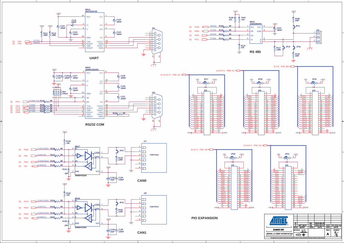
5
5
4
4
3
3
2
2
1
1
D D
C C
B B
A A
UART
RS 485
RS232 COM
(COM0_EN)
(UTXD)(URXD)
(TXD0)(RXD0)(RTS0)(CTS0)
(RXD0)
(RTS0)
(CTS0)
(CANTX0)
(CANRX0)
(CANTX0RS)
(CANRX0EN)
(CANRX1)
(CANTX1RS)
(CANRX1EN)
(CANTX1)
PIO EXPANSION
CAN0
CAN1
(TXD0)
PA18PA19PA20
PA6
PA9
PA11
PA14PA13
PA7PA8
PA12
PA10
PA15
PA22
PA27
PA23
PA29PA30
PA25
PA21
PA28
PA24
PA26
PA31
PA16PA17
PA0PA1PA2PA3PA4PA5
PB18PB19PB20
PB6
PB9
PB11
PB14PB13
PB7PB8
PB12
PB10
PB15
PB22
PB27
PB23
PB29PB30
PB25
PB21
PB28
PB24
PB26
PB31
PB16PB17
PB0PB1PB2PB3PB4PB5
PC18PC19PC20
PC6
PC9
PC11
PC14PC13
PC7PC8
PC12
PC10
PC15
PC22
PC27
PC23
PC29PC30
PC25
PC21
PC28
PC24
PC26
PC16PC17
PC0PC1PC2PC3PC4PC5
PD18PD19PD20
PD6
PD9
PD11
PD14PD13
PD7PD8
PD12
PD10
PD15
PD22
PD27
PD23
PD29PD30
PD25
PD21
PD28
PD24
PD26
PD16PD17
PD0PD1PD2PD3PD4PD5
PE6
PE9
PE11
PE14PE13
PE7PE8
PE12
PE10
PE15
PE29PE30
PE28
PE31
PE16PE0PE1PE2PE3PE4PE5
PE17
+3V3
+3V3 +3V3
+3V3
+3V3
+3V3
+3V3
+3V3
+3V3
+3V3
+3V3
+3V3+5V
+3V3+3V3 +3V3
+3V3+5V
+3V3 +3V3
+3V3+5V
+3V3
+3V3
+3V3+5V
+3V3 +3V3
+3V3+5V
+3V3
+3V3
PA9[3]PA8[3]
PA10[3]
PB26[3]
PE14[3]
PA11[3]
PB25[3]
PA10[3]
PB25[3]
PB26[3]
PA1[3]
PB20[3]
PA0[3]
PB21[3]
PB15[3]
PE15[3]
PB14[3]
PE16[3]
PA[0..31][2,3,4,5,6,7]
PB[0..31][2,3,5,6,7]
PC[0..30][3,4,5]
PD[0..30][3,4,6,7]
PE[0..31][2,3,5,6,7]
PA11[3]
REV DATEMODIF. DES. DATE VER.SCALE 1/1 REV. SHEET
This agreement is our property. Reproduction and publication without our written authorization shall expose offender to legal proceedings.
88A
XX-XXX-XXWL XXX
SERIAL & USER INTERFACES
2010-03-12
SAM3X-EK
INIT EDITAWL 2010-08-16B
REV DATEMODIF. DES. DATE VER.SCALE 1/1 REV. SHEET
This agreement is our property. Reproduction and publication without our written authorization shall expose offender to legal proceedings.
88A
XX-XXX-XXWL XXX
SERIAL & USER INTERFACES
2010-03-12
SAM3X-EK
INIT EDITAWL 2010-08-16B
REV DATEMODIF. DES. DATE VER.SCALE 1/1 REV. SHEET
This agreement is our property. Reproduction and publication without our written authorization shall expose offender to legal proceedings.
88A
XX-XXX-XXWL XXX
SERIAL & USER INTERFACES
2010-03-12
SAM3X-EK
INIT EDITAWL 2010-08-16B
C129100nFC129100nF
C127100nFC127100nF
R123 0RR123 0R
JP17JP171
2
3
J19J191 23 45 67 89 10
11 1213 1415 1617 1819 2021 2223 2425 2627 2829 3031 3233 3435 3637 3839 40
R134 0RR134 0R
R111100KR111100K
C124100nFC124100nF
R119 0RR119 0R
JP22JP22
R113 0RR113 0R
+ C13210uF
+ C13210uF
JP14JP14
C135100nFC135100nF
R10647KR10647K
JP15JP15 JP16JP16R11547KR11547K
MN15ADM3485ARZMN15ADM3485ARZ
RO1
RE2
DE3
DI4
VCC8
GND5
A6
B7
J20
CAN RJ12
J20
CAN RJ12
11
22
33
44
55
66
R130 0RR130 0R
C130100nFC130100nF
R138
10K
R138
10K
R13210KR13210K
J16J161 23 45 67 89 10
11 1213 1415 1617 1819 2021 2223 2425 2627 2829 3031 3233 3435 3637 3839 40
MN16ADM3312EARUMN16ADM3312EARU
C1+6
C1-20
C2+2
C2-4
C3+24
C3-22
VCC3
V+1
V-21
GND23
SD19
EN5
T1IN7
T1OUT18
R1IN15
R1OUT10
T2IN8
T2OUT17
R2IN14
R2OUT11
T3IN9
T3OUT16
R3IN13
R3OUT12
R135120RR135120R
JP21JP211
2
3
R12510KR12510K
J15J151 23 45 67 89 10
11 1213 1415 1617 1819 2021 2223 2425 2627 2829 3031 3233 3435 3637 3839 40
C128100nFC128100nF
R108DNPR108DNP
R129 0RR129 0R
R122 0RR122 0R
R117120RR117120R
R109 0RR109 0R
C1254.7uFC1254.7uF
R110 0RR110 0R
C120100nFC120100nF
C131100nFC131100nF
JP18JP181
2
3
R124 0RR124 0R
R114 0RR114 0R
R112100KR112100K
C121100nFC121100nF
R128120RR128120R
R127 0RR127 0R
Rs
D
EN
R
CANH
CANL
VCCGND
MN18
SN65HVD234
Rs
D
EN
R
CANH
CANL
VCCGND
MN18
SN65HVD234
2 3
7
6
4
1
5
8
J14J141 23 45 67 89 10
11 1213 1415 1617 1819 2021 2223 2425 2627 2829 3031 3233 3435 3637 3839 40
R10747KR10747K
C122100nFC122100nF
R137 0RR137 0R
R126 0RR126 0R
JP20JP201
2
3
C133100nFC133100nF
R133 0RR133 0R
R121 0RR121 0RR120 0RR120 0R
J18J181 23 45 67 89 10
11 1213 1415 1617 1819 2021 2223 2425 2627 2829 3031 3233 3435 3637 3839 40
MN14MAX3232CSEMN14MAX3232CSE
T1IN11
T2IN10 R1OUT12
R2OUT9
T1OUT14
T2OUT7R1IN13
R2IN8
V+2
C1+1
C1-3
C2+4
C2-5
V-6
VCC16
GND15
C126100nFC126100nF
JP19JP191
2
3
R118DNPR118DNP
JP23JP23
J11J11
5
4
3
2
1
9
8
7
6
10 11
J13J13
5
4
3
2
1
9
8
7
6
10 11
R131
10K
R131
10K
C123100nFC123100nF
R136 0RR136 0R
+ C13410uF
+ C13410uF
J12J121
2
3
RR747KX4RR747KX4
12345 6 7 8
J17
CAN RJ12
J17
CAN RJ12
11
22
33
44
55
66
C119100nFC119100nF
Rs
D
EN
R
CANH
CANL
VCCGND
MN17
SN65HVD234
Rs
D
EN
R
CANH
CANL
VCCGND
MN17
SN65HVD234
2 3
7
6
4
1
5
8
Section 6
Troubleshooting
6.1 Self-Test
A test package software is available to implement a functional test for each section of the board. Refer to the SAM3X-EK page on www.atmel.com.
6.2 Board Recovery
The SAM3X-EK is delivered with an on-board recovery procedure allowing to reprogram the board as it was when shipped. This procedure is accessible from the Flash disk mounted on a PC when the board is connected to this PC through the USB as described in Section 3.
SAM3X-EK User Guide 6-1
11156A–ATARM–25-May-12
Section 7
Revision History
7.1 Revision History
Table 7-1.
Document CommentsChange Request Ref.
11156A First issue.
SAM3X-EK User Guide 7-1
11156A–ATARM–25-May-12
11156A–ATARM–25-May-12 /xM
Headquarters International
Atmel Corporation2325 Orchard ParkwaySan Jose, CA 95131USATel: (+1) (408) 441-0311Fax: (+1) (408) 487-2600
Atmel Asia LimitedUnit 01-5 & 16, 19F BEA Tower, Millennium City 5 418 Kwun Tong Road Kwun Tong, Kowloon HONG KONG Tel: (+852) 2245-6100 Fax: (+852) 2722-1369
Atmel Munich GmbHBusiness CampusParkring 4D-85748 Garching b. MunichGERMANYTel: (+49) 89-31970-0 Fax: (+49) 89-3194621
Atmel Japan9F, Tonetsu Shinkawa Bldg.1-24-8 ShinkawaChuo-ku, Tokyo 104-0033JAPANTel: (81) 3-3523-3551Fax: (81) 3-3523-7581
Product Contact
Web Sitewww.atmel.comwww.atmel.com/AT91SAM
Technical SupportAT91SAM SupportAtmel technical support
Sales Contactswww.atmel.com/contacts/
Literature Requestswww.atmel.com/literature
Disclaimer: The information in this document is provided in connection with Atmel products. No license, express or implied, by estoppel or otherwise, to any intellectual property right is granted by this document or in connection with the sale of Atmel products. EXCEPT AS SET FORTH IN ATMEL’S TERMS AND CONDI-TIONS OF SALE LOCATED ON ATMEL’S WEB SITE, ATMEL ASSUMES NO LIABILITY WHATSOEVER AND DISCLAIMS ANY EXPRESS, IMPLIED OR STATUTORY WARRANTY RELATING TO ITS PRODUCTS INCLUDING, BUT NOT LIMITED TO, THE IMPLIED WARRANTY OF MERCHANTABILITY, FITNESS FOR A PARTICULAR PURPOSE, OR NON-INFRINGEMENT. IN NO EVENT SHALL ATMEL BE LIABLE FOR ANY DIRECT, INDIRECT, CONSEQUENTIAL, PUNITIVE, SPECIAL OR INCIDEN-TAL DAMAGES (INCLUDING, WITHOUT LIMITATION, DAMAGES FOR LOSS OF PROFITS, BUSINESS INTERRUPTION, OR LOSS OF INFORMATION) ARISING OUT OF THE USE OR INABILITY TO USE THIS DOCUMENT, EVEN IF ATMEL HAS BEEN ADVISED OF THE POSSIBILITY OF SUCH DAMAGES. Atmel makes no representations or warranties with respect to the accuracy or completeness of the contents of this document and reserves the right to make changes to specifications and product descriptions at any time without notice. Atmel does not make any commitment to update the information contained herein. Unless specifically provided otherwise, Atmel products are not suitable for, and shall not be used in, automotive applications. Atmel’s products are not intended, authorized, or warranted for use as components in applications intended to support or sustain life.
© 2012 Atmel Corporation. All rights reserved. Atmel®, Atmel logo and combinations thereof, QTouch®, DataFlash®, SAM-BA® and others are registered trademarks or trademarks of Atmel Corporation or its subsidiaries. Windows® and others, are registered trademarks or trade-marks of Microsoft Corporation in the US and/or other countries. ARM®, ARM®Powered logo, Cortex®, Thumb®-2 and others are registered trademarks or trademarks of ARM Ltd. Other terms and product names may be trademarks of others.