Embed Size (px)
Citation preview
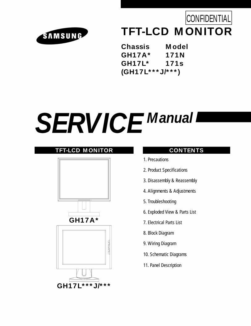
TFT-LCD MONITORChassis ModelGH17A* 171NGH17L* 171s(GH17L***J/***)
ManualSERVICETFT-LCD MONITOR CONTENTS
1. Precautions
2. Product Specifications
3. Disassembly & Reassembly
4. Alignments & Adjustments
5. Troubleshooting
6. Exploded View & Parts List
7. Electrical Parts List
8. Block Diagram
9. Wiring Diagram
10. Schematic Diagrams
11. Panel Description
CONFIDENTIAL
GH17A*
GH17L***J/***
2 Product Specifications
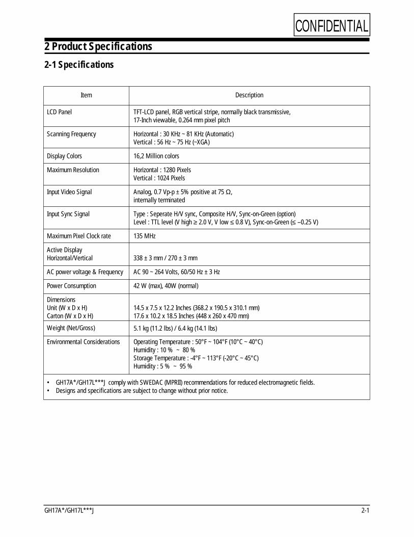
2-1 Specifications
LCD Panel TFT-LCD panel, RGB vertical stripe, normally black transmissive, 17-Inch viewable, 0.264 mm pixel pitch
Scanning Frequency Horizontal : 30 KHz ~ 81 KHz (Automatic) Vertical : 56 Hz ~ 75 Hz (~XGA)
Display Colors 16,2 Million colors
Maximum Resolution Horizontal : 1280 Pixels Vertical : 1024 Pixels
Input Video Signal Analog, 0.7 Vp-p ± 5% positive at 75 Ω,internally terminated
Input Sync Signal Type : Seperate H/V sync, Composite H/V, Sync-on-Green (option)Level : TTL level (V high ≥ 2.0 V, V low ≤ 0.8 V), Sync-on-Green (≤ –0.25 V)
Maximum Pixel Clock rate 135 MHz
Active DisplayHorizontal/Vertical 338 ± 3 mm / 270 ± 3 mm
AC power voltage & Frequency AC 90 ~ 264 Volts, 60/50 Hz ± 3 Hz
Power Consumption 42 W (max), 40W (normal)
DimensionsUnit (W x D x H) 14.5 x 7.5 x 12.2 Inches (368.2 x 190.5 x 310.1 mm)Carton (W x D x H) 17.6 x 10.2 x 18.5 Inches (448 x 260 x 470 mm)
Weight (Net/Gross)
Environmental Considerations Operating Temperature : 50°F ~ 104°F (10°C ~ 40°C)Humidity : 10 % ~ 80 %Storage Temperature : -4°F ~ 113°F (-20°C ~ 45°C)Humidity : 5 % ~ 95 %
• GH17A*/GH17L***J comply with SWEDAC (MPRII) recommendations for reduced electromagnetic fields.• Designs and specifications are subject to change without prior notice.
Description
5.1 kg (11.2 lbs) / 6.4 kg (14.1 lbs)
GH17A*/GH17L***J 2-1
Item
CONFIDENTIAL
CONFIDENTIAL2 Product Specifications
2-2 GH17A*/GH17L***J
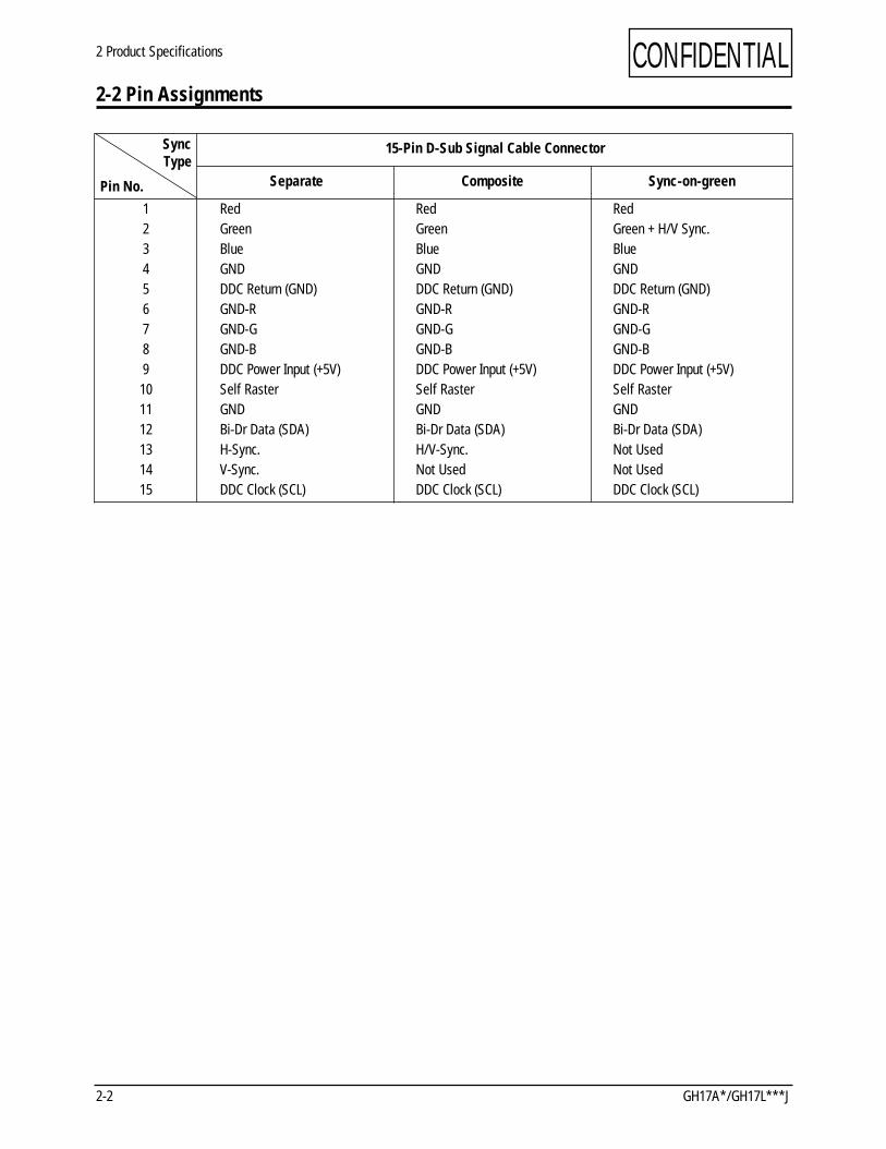
2-2 Pin Assignments
SyncType
Pin No.
15-Pin D-Sub Signal Cable Connector
Separate Composite
123456789
101112131415
RedGreenBlueGNDDDC Return (GND)GND-RGND-GGND-BDDC Power Input (+5V)Self RasterGNDBi-Dr Data (SDA)H-Sync.V-Sync.DDC Clock (SCL)
RedGreenBlueGNDDDC Return (GND)GND-RGND-GGND-BDDC Power Input (+5V)Self RasterGNDBi-Dr Data (SDA)H/V-Sync.Not UsedDDC Clock (SCL)
RedGreen + H/V Sync.BlueGNDDDC Return (GND)GND-RGND-GGND-BDDC Power Input (+5V)Self RasterGNDBi-Dr Data (SDA)Not UsedNot UsedDDC Clock (SCL)
Sync-on-green
CONFIDENTIAL2 Product Specifications
GH17A*/GH17L***J 2-3
Q R S
P
O
Video
Sync Sync
Horizontal Vertical
C D E
P
O
B
A
Video
Sync Sync
Separate Sync
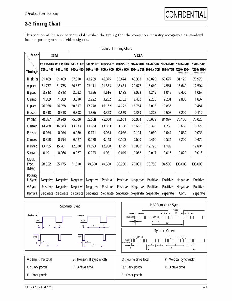
2-3 Timing Chart
This section of the service manual describes the timing that the computer industry recognizes as standardfor computer-generated video signals.
C D
A O
E
B P
Video
Sync Sync
Video
Q R S
A : Line time total B : Horizontal sync width O : Frame time total P : Vertical sync width
C : Back porch D : Active time Q : Back porch R : Active time
E : Front porch S : Front porch
VIDEOA
B OP
Q R S
Horizontal Vertical
B
GreenVertical
P Q R SO
Horizontal
H/V Composite Sync
Sync-on-Green
79.976
12.504
1.067
1.837
9.481
0.119
75.025
13.329
0.038
0.475
12.804
0.013
135.000
Positive
Positive
Separate
81.129
16.640
6.400
2.880
3.200
76.106
10.660
0.080
3.200
0.020
135.000
Negative
Negative
Com.
68.677
14.561
1.016
2.201
10.836
0.508
84.997
11.765
0.044
0.524
11.183
0.015
94.500
Positive
Positive
Separate
1024/85Hz1024x768
1280/76Hz1280x1024
1280/75Hz1280x1024
1024/75Hz1024 x 768
60.023
16.660
1.219
2.235
13.003
0.203
75.029
13.328
0.050
0.466
12.795
0.017
78.750
Positive
Positive
Separate
31.469
31.777
3.813
1.589
26.058
0.318
70.087
14.268
0.064
0.858
13.155
0.191
28.322
Negative
Positive
Separate
fH (kHz)
A µsec
B µsec
C µsec
D µsec
E µsec
fV (Hz)
O msec
P msec
Q msec
R msec
S msec
ClockFreq.(MHz)
PolarityH.Sync
V.Sync
Remark
IBM
640/75 Hz640 x 480
640/85 Hz640 x 480
800/75 Hz800 x 600
800/85 Hz800 x 600
1024/60Hz1024 x 768
VGA2/70 Hz720 x 400
VGA3/60 Hz640 x 480
Table 2-1 Timing Chart
31.469
31.778
3.813
1.589
26.058
0.318
59.940
16.683
0.064
0.794
15.761
0.064
25.175
Negative
Negative
Separate
37.500
26.667
2.032
3.810
20.317
0.508
75.000
13.333
0.080
0.427
12.800
0.027
31.500
Negative
Negative
Separate
43.269
23.111
1.556
2.222
17.778
1.556
85.008
11.764
0.671
0.578
11.093
0.023
49.500
Negative
Negative
Separate
46.875
21.333
1.616
3.232
16.162
0.323
75.000
13.333
0.064
0.448
12.800
0.021
49.500
Positive
Positive
Separate
53.674
18.631
1.138
2.702
14.222
0.569
85.061
11.756
0.056
0.503
11.179
0.019
56.250
Positive
Positive
Separate
48.363
20.677
2.092
2.462
15.754
0.369
60.004
16.666
0.124
0.600
15.880
0.062
75.000
Negative
Negative
Separate
Mode VESA
Timing (Analog Only) (Analog Only)
GH17A*/GH17L***J 3-1
3 Disassembly and ReassemblyThis section of the service manual describes the disassembly and reassembly procedures for theGH17A*/GH17L***J TFT-LCD monitors.
WARNING: This monitor contains electrostatically sensitive devices. Use caution when handling
these components.
3-1 Disassembly (GH17A*)
Cautions:1. Disconnect the monitor from the power source before disassembly.2. Follow these directions carefully; never use metal instruments to pry apart the cabinet.
CONFIDENTIAL
3-1-1 Removing the Stand
1. With a pad beneath it, stand the monitor on its front with the screen facing downward and the base close to you. Make sure nothing will damage the screen.
2. Remove the 4 screws on the Stand.
Caution: Be careful. The signal cable and power cable are still attached to the monitor.
3. Disconnect the Signal Cable and Power Cord.
3-1-2 Main Body Disassembly
1. Pull the Rear Cover up and off the monitor.2. Disconnect the Function PCB wire (8P) between the Function PCB and the CN108 connector on
the Main PCB.3. Remove 10 screws on the PCB Shield.4. Disconnect 4 Inverter wires between the panel and the CN2, 3, 4, 5 connectors on the Inverter PCB.5. Disconnect the Interface wire (30P) between the panel and the CN301 connector on the Main PCB.6. Remove 2 screws on the Main PCB and 2 screws on the Inverter PCB and 2 screws on the Power
Adapter PCB.7. Disconnect the 12P harness between CN1 connector on the inverter and CN104 connector on the
Main PCB.8. Carefully lift the Main PCB Assembly and Inverter PCB and place them on a flat, level surface that
is protected from static electricity
3 Disassembly and Reassembly
3-2 GH17A*/GH17L***J
CONFIDENTIAL
1. Push the jig deep in the opening hole
2. Push down the jig and pull up the rear covertill it opens.
3. Do the step 2 in opposite side until it opens.
4. Rear cover until it opens.
3-1-3 Disassembly (GH17A*)
Reassembly procedures are in the reverse order of Disassembly procedures.
3 Disassembly and Reassembly
GH17A*/GH17L***J 3-3
CONFIDENTIAL3-2 Disassembly (GH17L***J)
Cautions:1. Disconnect the monitor from the power source before disassembly.2. Follow these directions carefully; never use metal instruments to pry apart the cabinet.
3-2-1 Removing the Stand
1. With a pad beneath it, stand the monitor on its front with the screen facing downward and the base close to you. Make sure nothing will damage the screen.
2. Remove the 4 screws on the Stand.
Caution: Be careful. The signal cable and power cable are still attached to the monitor.
3. Disconnect the Signal Cable and Power Cord.
3-2-2 Main Body Disassembly
1. Remove 5 screws on the Rear Cover.2. Pull the Rear Cover up and off the monitor.3. Remove 7 screws on the PCB Shield.4. Disconnect the Function PCB wire(10P) between the Function PCB and the CN103 connector
on the Main PCB.5. Disconnect 4 Inverter wires between the panel and the CN2, 3, 4, 5, connectors on the Inverter PCB.6. Disconnect the Interface wire(30P) between the panel and the CN301 connector on the Main PCB.7. Remove 2 screws on the Main PCB and 2 screws on the Inverter PCB and 2 screws on the Power
Adapter PCB.8. Disconnect the 12P harness between CN1 connector on the inverter and CN104 connector on the
Main PCB.9. Carefully lift the Main PCB Assembly and Inverter PCB and place them on a flat, level surface
that is protected from static electricity.10. Remove 3 screws on the Function PCB from the Front Cover and remove the Function PCB and
Function Knob.
3-3 Reassembly
Reassembly procedures are in the reverse order of Disassembly procedures.
CONFIDENTIAL
GH17A*/GH17L***J 5-1
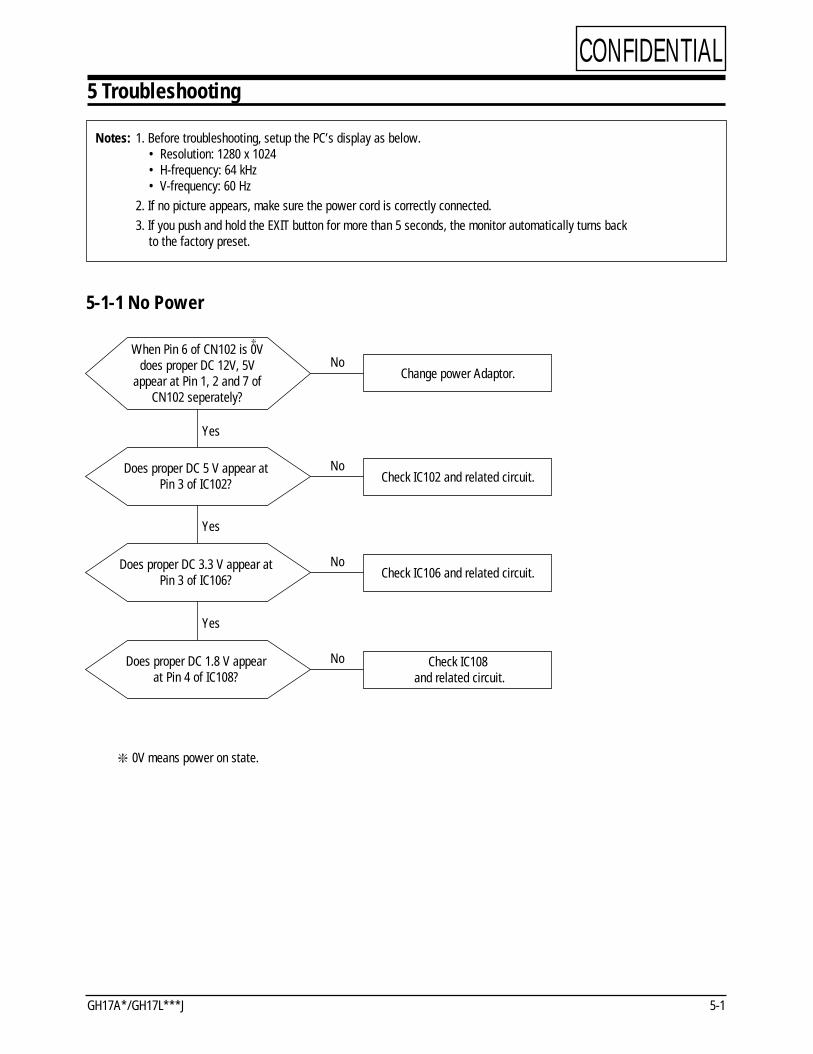
5 Troubleshooting
Notes: 1. Before troubleshooting, setup the PC’s display as below.• Resolution: 1280 x 1024• H-frequency: 64 kHz• V-frequency: 60 Hz
2. If no picture appears, make sure the power cord is correctly connected.3. If you push and hold the EXIT button for more than 5 seconds, the monitor automatically turns back
to the factory preset.
5-1-1 No Power
When Pin 6 of CN102 is 0V does proper DC 12V, 5V
appear at Pin 1, 2 and 7 of CN102 seperately?
Change power Adaptor.
Yes
No
Does proper DC 5 V appear at Pin 3 of IC102? Check IC102 and related circuit.
Yes
No
Does proper DC 3.3 V appear at Pin 3 of IC106? Check IC106 and related circuit.
No
Yes
Does proper DC 1.8 V appear at Pin 4 of IC108?
Check IC108and related circuit.
No
0V means power on state.
CONFIDENTIAL5 Troubleshooting
5-2 GH17A*/GH17L***J
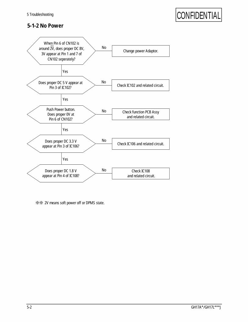
5-1-2 No Power
When Pin 6 of CN102 is around 2V, does proper DC 8V,
3V appear at Pin 1 and 7 ofCN102 seperately?
Change power Adaptor.
Yes
Yes
No
Push Power button.Does proper 0V at Pin 6 of CN102?
Check function PCB Assy and related circuit.
Yes
No
Does proper DC 3.3 V appear at Pin 3 of IC106? Check IC106 and related circuit.
No
Yes
Does proper DC 1.8 V appear at Pin 4 of IC108?
Check IC108and related circuit.
No
Does proper DC 5 V appear at Pin 3 of IC102? Check IC102 and related circuit.
No
2V means soft power off or DPMS state.
CONFIDENTIAL
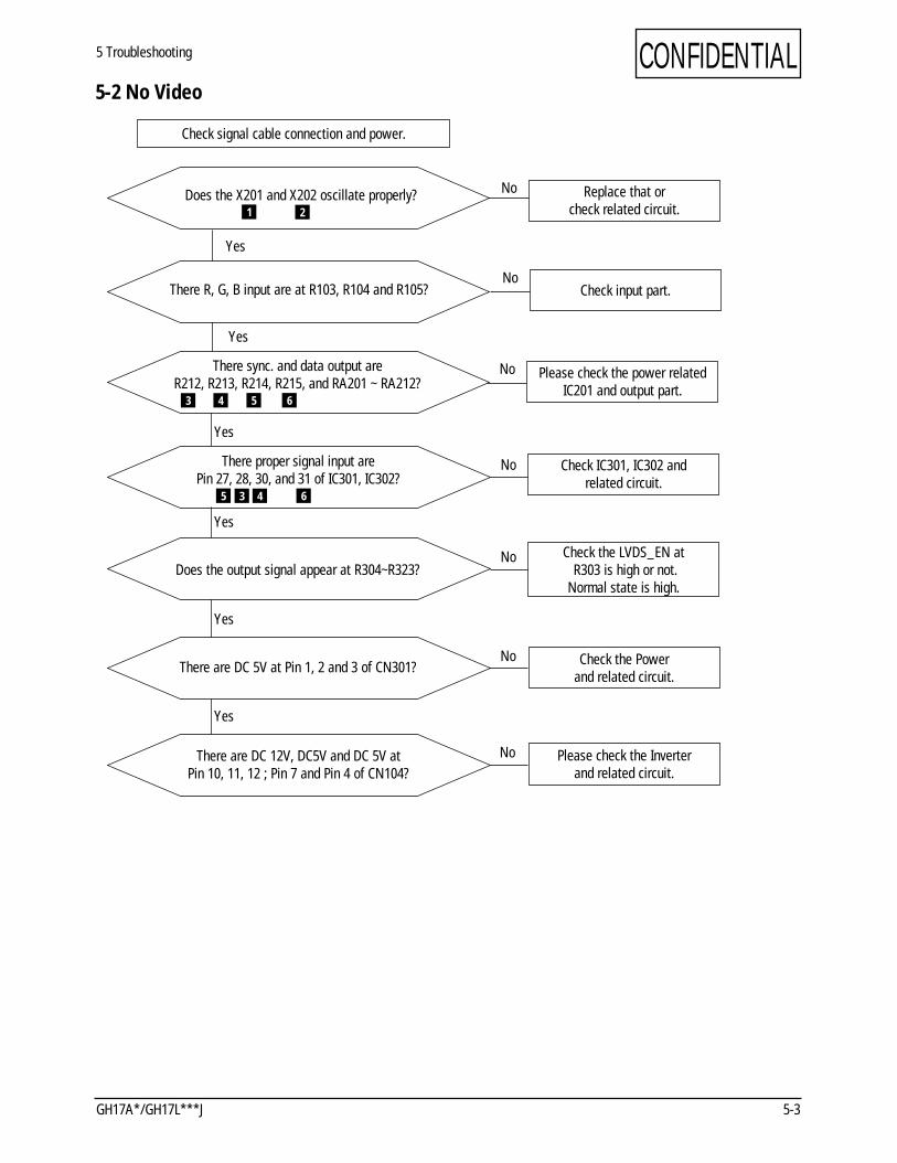
There sync. and data output areR212, R213, R214, R215, and RA201 ~ RA212?
5 Troubleshooting
GH17A*/GH17L***J 5-3
5-2 No Video
Check signal cable connection and power.
Check IC301, IC302 and related circuit.
Yes
NoThere proper signal input arePin 27, 28, 30, and 31 of IC301, IC302?
Yes
Check the LVDS_EN atR303 is high or not.
Normal state is high.Does the output signal appear at R304~R323?
Yes
No
Check the Power and related circuit.
No
Please check the Inverter and related circuit.
No
There are DC 5V at Pin 1, 2 and 3 of CN301?
Yes
There are DC 12V, DC5V and DC 5V at Pin 10, 11, 12 ; Pin 7 and Pin 4 of CN104?
3 4 5
Does the X201 and X202 oscillate properly?
Yes
There R, G, B input are at R103, R104 and R105?
Replace that or check related circuit.
No
Check input part.No
Please check the power relatedIC201 and output part.
No
Yes
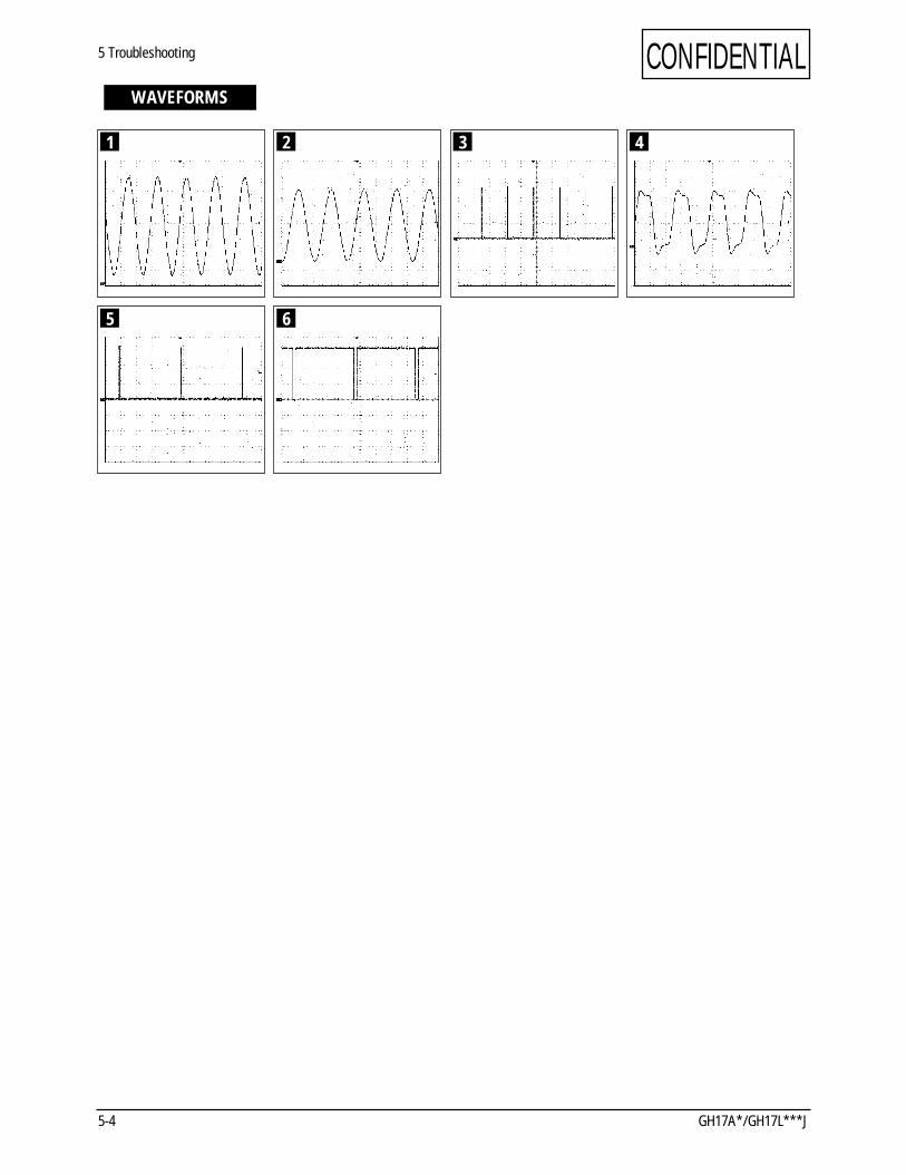
1 2
6
3 45 6
CONFIDENTIAL5 Troubleshooting
5-4 GH17A*/GH17L***J
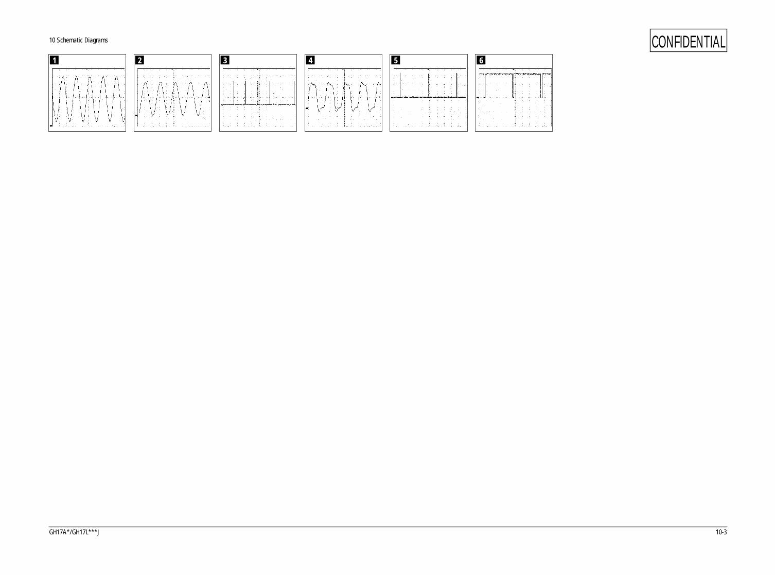
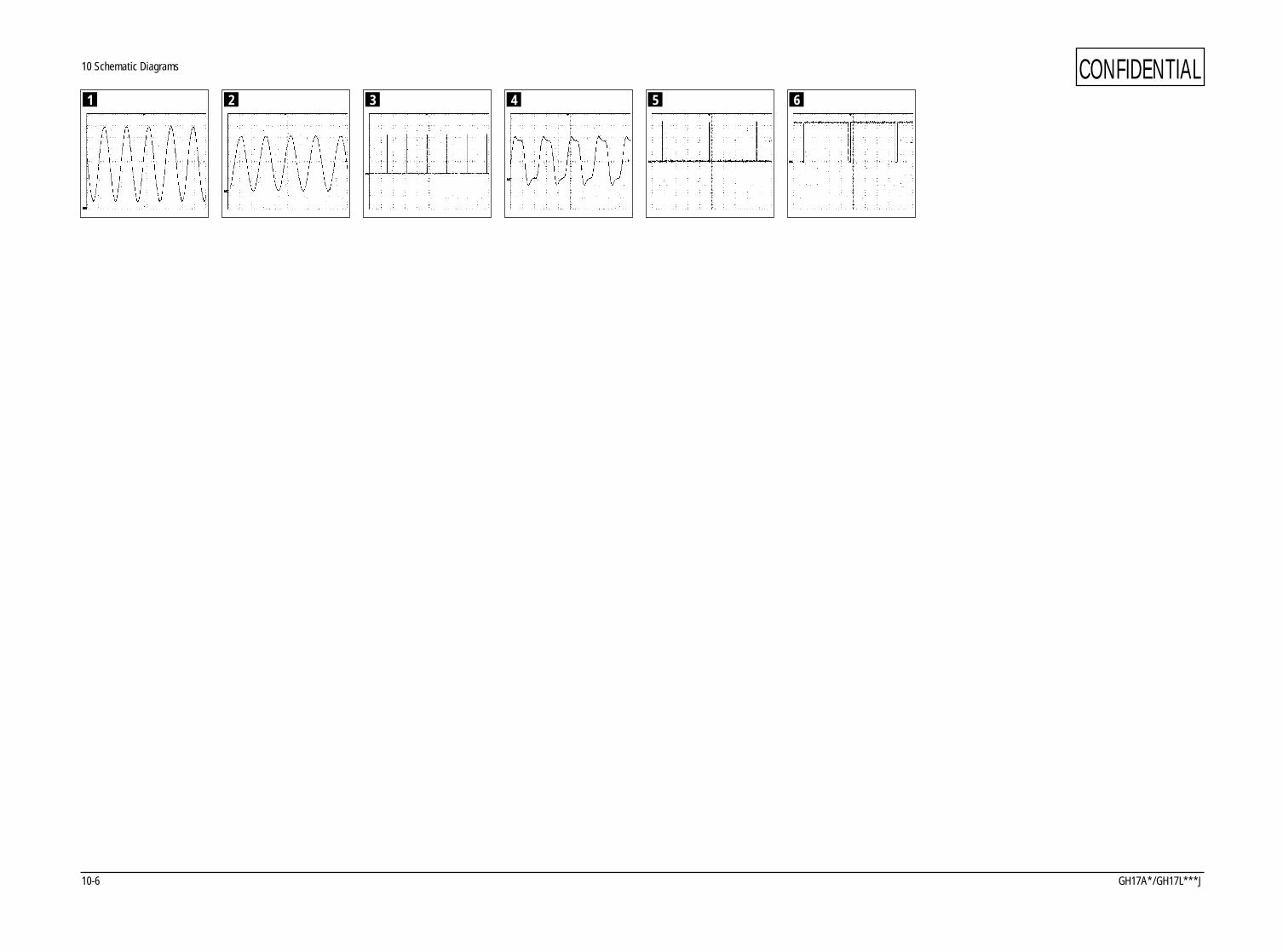
WAVEFORMS
1 2
5 6
3 4
CONFIDENTIAL
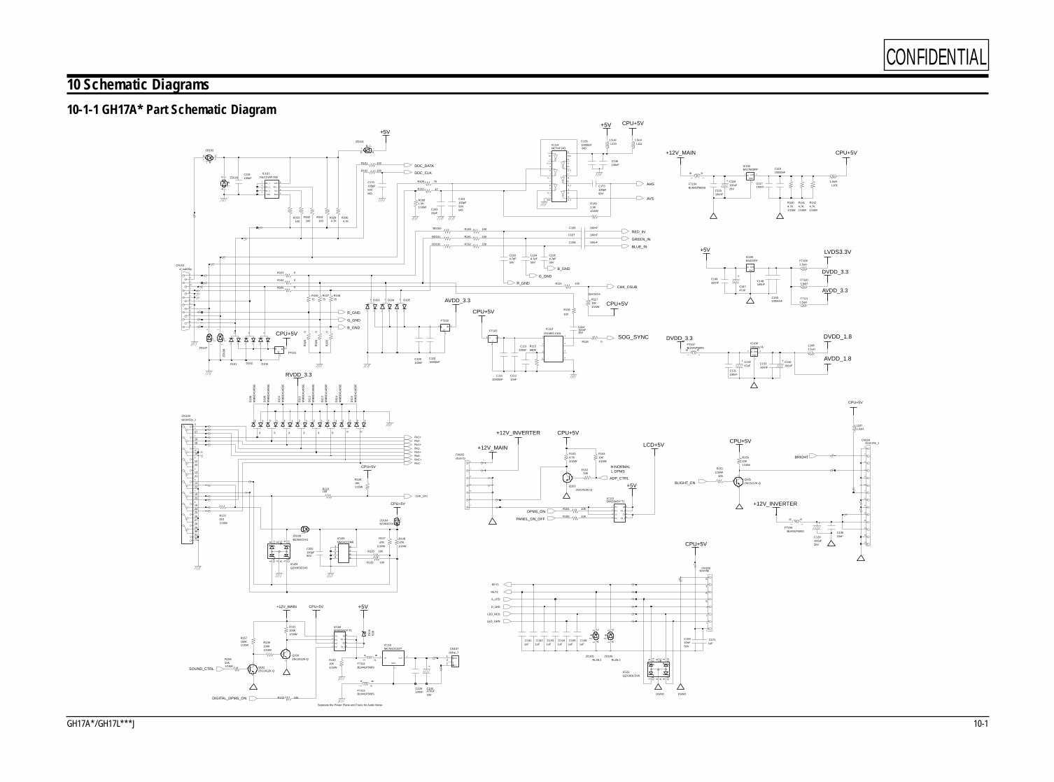
GH17A*/GH17L***J 10-1
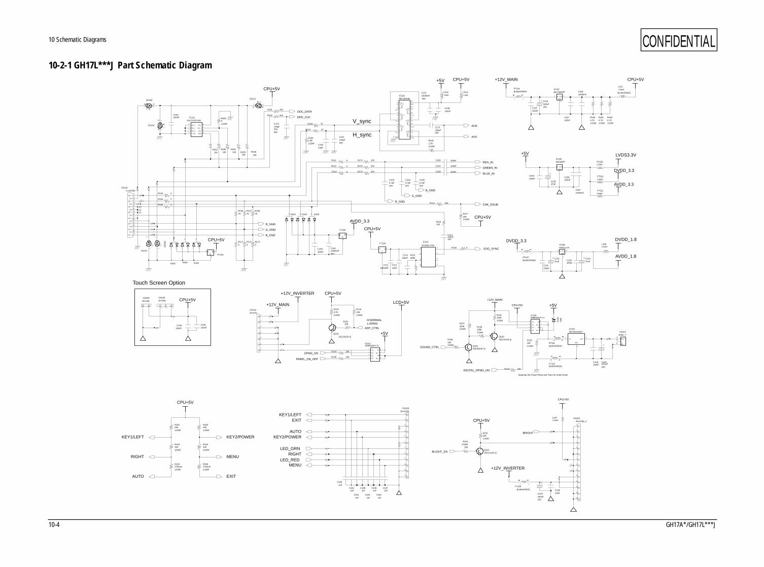
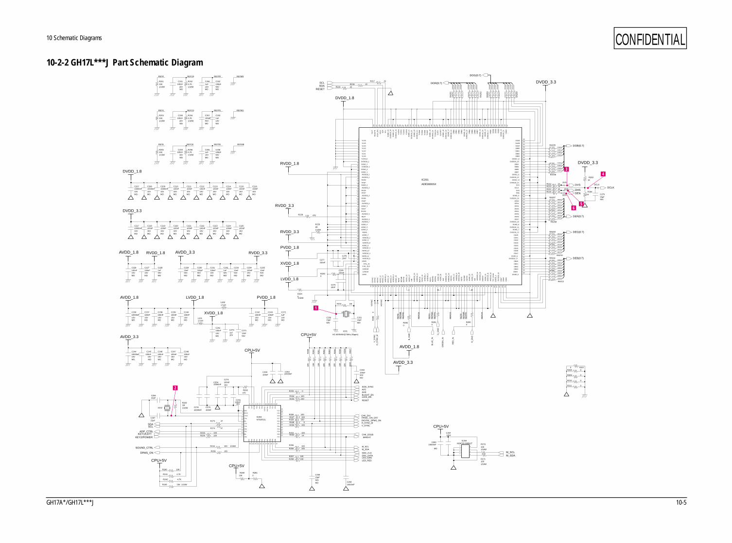
10 Schematic Diagrams
10-1-1 GH17A* Part Schematic Diagram
L:DPMSH:NORMAL
Seperate the Power Plane and Trace for Audio Noise
R101 100
1
NC_3 SCL 6
SDA 5
VCC 8
4VSS
WC_ 7
R138
1/16W100K
IC10124LC21AT-/SN
1NC_1
2NC_2
3
MM
BD
4148
SE
D11
5
12
3
78
100nFC149
NM24C02M8IC105
1234 5
6
R11710K1/16W
2
3
+5VBD102
1
B2
D11
3M
MB
D41
48S
E
1
BLM41P600SFT104
A
BLM41P600SFT107
A1
B2
BD101
+12V_INVERTER
DVDD_1.8
LCD+5V
BD100
FAN1117AIC108
GND
1
IN3 OUT 4
CPU+5V
10K1/16W
R124
R1404.7K1/16W
+12V_MAIN
100nFC148
C1451uF
100nFC108
+5V
C107 100nF
1
100nFC106
ZD104BZX84C5V1
C131100nF
1uF
R14410K1/16W
1/16W100KR157
C146
MM
BD
4148
SE
D11
2
12
31
1
CPU+5V
1uF
1
R1424.7K1/16W
C144
1
DVDD_3.3
1
C13247uF
C141
22pFC102
3 C
1uF
RLZ8.2ZD105
A12
B
1uFC142
C11110000nF
AVDD_3.3
R128
1/16W47K
ZD103
A 1
2B
3C
BLM41P600SFT106
A1
B2
R109
1/16W10KR133
L1101.5uH
75
G24
1 S1
3 S2
CPU+5V
1
IC112SI9933ADY-T1
D1 8
7D1_1
D2 6
5D2_1
G12
R10875
27
303132
100R160
16
26
29
17
18
19
20
21
22
23
24
7
8
25
28
9
10
11
12
13
14
15
CN109tpcon32p_1
1
2
3
4
5
6
CPU+5V
RVDD_3.3
0R
164
1
NC5
R16
30
QZX363C5V6IC111
A2C
16 C24
C3
3C4
75
C13010nF
2SC2412K-QQ103
B
C
E
R107
1
12
3
C252100pF50V
10K1/16W
R158
MM
BD
4148
SE
D10
8
R102
1.5uHFT111
100
D105
1 2
3
1 2
3
+12V_INVERTER
D103
3
C
D11
6S
2B
C1054.7pF50V
ZD101
A1
2B
10000nFC150
1.5uHL101
1 OUT 3
1
CPU+5V
4
5
6
7
BA17805FPIC102
2
GND
IN
CN102slcon7p
1
2
3
1.5uH
R161 100
1/16W1.5KR146
L108
50V100pFC173
1.5uHL111
1 2
3
C151100nF
10K
CPU+5V
D101
1
R152
C1711uF
1
+5V
2
3
BZX84C5V1ZD109
D104
1
MM
BD
4148
SE
12
3
100R162
D11
1
1
Q1022SC2412K-Q
B
C
E
CN107dcjhp_7
1
23
R115680K
100K1/16W
R131
+12V_MAIN
1
47K1/16W
R127
1
A1
2 B3
C
C170100pF50VMO
0
ZD102
1uFC143
R16
5
C16010nF50V
C109100nF
R118 0
1.5uHFT110
100
100
+5V
R116
R125
A1
B2
R1434.7K1/16W
CPU+5V
BLM41P600SFT113
A12
B3 C
R132 10K
12
13
14
15
ZD106RLZ8.2
1
2
3
4
5
6
7
8
9
10
11
D10
9M
MB
D41
48S
E
12
3
d_sub15pCN101
R333100 100
R332
2 A
6 C1 4
C2
3 C3
1 C4
5N
C
1
+12V_MAIN
IC104QZX363C5V6
100nFC136
14
VCC
+5V
MO10000nFC135
I2
9
I3
11
I4
13
I5
1
IO
4
O_1
O_2
6
8
O_3
10
O_4
12
O_5
2
O_O
GND
IN OUT
IC114MC74F14D
7
GND
3
I1
5
1/16W510
IC106BA033FP
C113100nF
R122
10000nFC110
100nFC117
R114
LVDS3.3V
R10675
100
C134100uF
R15010K1/16W
MO50V100pFC101
AVDD_1.8
C1034.7pF50V
1
R151
1
0R105
1/16W10K
A1B
2
3
C
0R104
FT103
D102
1 2
3
AVDD_3.3
50V4.7pFC104
R110 47
1.5uHL107
100R126
D106
1 2
3
DVDD_3.3
CPU+5V
1
1
2
3
CPU+5V
10000nFC118
ZD
108
1
1.5uHFT109
1
2
3
47uFC147
4.7KR330
ZD107
2
3
10KR154
C112
MM
BD
4148
SE
D11
4
1
25V100uFC129
10nF
Q1012SC2412K-Q
B
C
E
FT112BLM41P600S
1A
2B
CPU+5V
MC7812CD2TIC110
GND
2
IN1
OUT3
slcon8pCN108
1
2
3
4
5
6
7
8
0R103
7
8
9
10
11
12
13
14
slcon14p_1CN104
1
2
3
4
5
6
E
C114
16V100nF
1
Q1002SC2412K-Q
B
C
C133100nF
1
R3294.7K
R331100
MM
BD
4148
SE
D11
0
12
3
R1901.5K1/16W
CPU+5V
A 12 BC
3
1
8
1
FT101
IC113
GS1881-CKA1
2
3
45
6
7
C115100nF
1/16W4.7KR141
R156
C140470UF16V
B
3
C
10K
FT102
1A2
100
25V100uFC116
CPU+5V
R123
100nFC139
D1
D1_1 7
6D2
D2_1 5
2G1
4 G2
S11
S23
AHS
SI9933ADY-T1IC109
8
DDC_CLK
DGND
AVS
G_GND
DIGITAL_DPMS_ON
BLIGHT_EN
SOUND_CTRL
BLUE_IN
GREEN_IN
RED_IN
R_GND
G_GND
B_GND
R_GND
B_GND
ADP_CTRL
Rx1-
Rx2+
Rx1+
CHK_DVI
KEY1
D_LED
LED_RED
A_LED
LED_GRN
KEY2
DGND
Rx0-Rx0+
RxC+RxC-
Rx2-
tjunctions
CHK_DSUB
SOG_SYNC
BRIGHT
DPMS_ON
PANEL_ON_OFF
DDC_DATA
MO50V100pFC206
C2031uF10VMO
R293
R29
10
0
1001/16W
50
7YUV0
YUV16
5YUV2
4YUV3
3YUV4
YUV52
1YUV6
208
YU
V7
YUVCLK8
R271
188
TC
ON
6
TC
ON
718
7
184
TC
ON
_IN
99T
ST
_SC
AN
VS
YN
C54
XC
LK20
5
206
XC
LK_E
N
47XGND
XTAL_IN48
49XTAL_OUT
XVDD18
17RX2P
RXCM28
27RXCP
SC
L20
3
204
SD
A
198
TC
ON
0
TC
ON
119
7
196
TC
ON
2
TC
ON
319
5
190
TC
ON
4
TC
ON
518
9
RE
FP
B
77R
EF
PG
89R
EF
PR
RE
FR
87
RE
SE
TN
207
REXT30
23RX0M
RX0P24
RX1M20
21RX1P
RX2M16
139OVS
RBIAS36
RE
FB
63 71R
EF
CB
RE
FC
G83 95
RE
FC
R
75R
EF
G
RE
FM
B64
RE
FM
G76
RE
FM
R8865
128
127ORA6
ORA7126
OR
B0
177
OR
B1
176
175
OR
B2
OR
B3
174
171
OR
B4
OR
B5
170
169
OR
B6
OR
B7
168
160
157
OG
B4
OGB5156
OGB6155
OGB7154
137OHS
133ORA0
ORA1132
131ORA2
ORA3130
129ORA4
ORA5
119OGA1
OGA2118
117OGA3
OGA4116
115OGA5
OGA6114
113OGA7
163
OG
B0
OG
B1
162
161
OG
B2
OG
B3
OBB0
OBB1152
151OBB2
150OBB3
147OBB4
OBB5146
145OBB6
OBB7144
OCLK138
ODE136
OGA0120
92
LGND52
51LVDD18
110OBA0
109OBA1
OBA2108
107OBA3
OBA4106
OB
A5
104
103
OB
A6
OB
A7
102
153
111DVDD33_17
125DVDD33_18
DVDD33_19134
DVDD33_20148
DV
DD
33_2
115
8
DV
DD
33_2
217
2
DV
DD
33_2
318
5
55H
SY
NC
INB
68
ING
80
INR
142
DV
DD
18_1
716
4
DV
DD
18_1
816
6
178
DV
DD
18_1
9
11DVDD18_2
DV
DD
18_2
018
0
DV
DD
18_2
119
1
DV
DD
18_2
219
3
DV
DD
18_2
319
9
DV
DD
18_2
420
1
101
DV
DD
33_1
6
12
DG
ND
_410
0
105DGND_5
112DGND_6
DGND_7122
DGND_8124
135DGND_9
9DVDD18_1
121DVDD18_13
123DVDD18_14
DVDD18_15140
DVDD18_16
167
DG
ND
_15
173
DG
ND
_16
179
DG
ND
_17
181
DG
ND
_18
186
DG
ND
_19
DGND_210
192
DG
ND
_20
194
DG
ND
_21
200
DG
ND
_22
202
DG
ND
_23
DGND_3
AVDD33_840
AV
DD
33_9
58 59A
VD
D_1
0
CLK
IN18
3
182
CLK
OU
T
53C
SY
NC
141DGND_10
143DGND_11
149DGND_12
159
DG
ND
_13
165
DG
ND
_14
70 81A
VD
D33
_12
AV
DD
33_1
382 93
AV
DD
33_1
4
AV
DD
33_1
594
19AVDD33_2
AVDD33_322
25AVDD33_4
29AVDD33_5
31AVDD33_6
AVDD33_732
AVDD18_238
AVDD18_342
AVDD18_444
AVDD18_546
AV
DD
18_6
61 73A
VD
D18
_7
AV
DD
18_8
74
AV
DD
18_9
85
15AVDD33_1
69A
VD
D33
_10
AV
DD
33_1
1
AGND_326
33AGND_4
AGND_534
35AGND_6
37AGND_7
39AGND_8
41AGND_9
AVDD18_114
AV
DD
18_1
086 97
AV
DD
18_1
1
AV
DD
18_1
29862
AG
ND
_16
66 67A
GN
D_1
7
AG
ND
_18
72
AG
ND
_19
78
AGND_218
79A
GN
D_2
0
AG
ND
_21
84
AG
ND
_22
90 91A
GN
D_2
3
AG
ND
_24
96
AGND_113
43AGND_10
45AGND_11
AG
ND
_12
56 57A
GN
D_1
3
AG
ND
_14
60
AG
ND
_15
CPU+5V
IC201
ADE3000SX
4.7KR242
R241 4.7K
R229
R26
718
0K
4
56
78
1/16W2K
8
RA211
12
312
34
56
7
R256
RA209
R26
3
XVDD_1.8
100
C222100nF16VMO
10K
0R211
0
RVDD_3.3
CPU+5V
MO50V100pFC202
AVDD_3.3
R208
MO16V100nFC238
100
100nF
R2551/16W100R244
C249
C218100nF16VMO
MO16V100nFC216
10V1uFC273
DVDD_3.3
RVDD_3.3
C2721uF10VMO
10nF50VMO
C22910nF50VMO
C235
0
MO10V10000nFC207
R210
C25310000nF
MO
C230100pF50VMO
C23310nF50V
L2011.5uH
DHS
R231 1M
DVS
1
2
3
4 5
6
7
8
16V100nFC221
RVDD_1.8
IC204M24C08-WMN1T
R29
20
MO
2
34
56
78
RA205
1
C231100nF16VMO
MO16V100nFC225
C255100nF
16VR233
R2701001/16W
C201
1/16W1M
MO16V
100nF
4.7K1/16W
R204
CPU+5V
470R228
R26
510
K
47R274
R26
210
K
10K
R221 10
R280
R258
0 R207
100
MO10V10000nFC244
15K1/16W
R203
C226100nF16VMO
MO16V100nFC212
C245100nF
16VMO
10VMO
C267100pF50VMO
DVDD_3.3
C2661uF
50V12pFC250
100R239
C246100nF16VMO
1/16W4.7KR202
MO16V
100nFC204
22pFC256
DVDD_1.8
R235 100
XVDD_1.8
C215100nF16VMO
10
12
34
56
78
R226
RA208
22R218
DCLK
100R327
C25910000nF
R224
10R222
MO16V100nFC223
10
R249
R254 1K
0100R250
C25410000nF
CPU+5V
X202
PD035
34PD1
33PD2
32PD3
31PD4
30PD5
RS
TB
4
V33
6 44
VS
YN
CI
27
PB
5
26
PB
6
25
PB
7
PC
0
3
PC
1
2
PC
2
1 42
PC
3
41
PC
4
40
PC
5
37PC6
PC736
PA
2
PA
3
22
PA
4
21
PA
5
20
PA
6
19
PA
7
18
PB017
PB116
PB215
PB314
28
PB
4
NC138
NC239
9OSCI
8OSCO
10P30
11P31
12P34
P3513
29PA0
24
PA
1
23
NT68F63LIC202
CV
V
5
GND7
43
HS
YN
CI
C23610000nF10VMO
MO50V100nFC260
100R328
C25722pF
R26
610
KMO16V100nFC242
L2021.5uH
HC-49/SM5H(27MHz,30ppm)Q0 Q1
R273 47
DVDD_1.8
X201MO16V100nFC240
C26310000nF
MO
LVDD_1.8
C234100nF16VMO
AVDD_3.3
12
34
56
78
LVDD_1.8
RA212
MO16V100nFC239
10K
R26
4
R243
MO50V15pFC258
22R215
0
100nF16VMO
RVDD_3.3
C248
MO10V1uFC205
AVDD_1.8
C241100nF16V
MO50V10nFC275
C251
16V100nFC219
10pF50V
R26
1
AVDD_1.8
MO
2
3
4
5
6
7
8
10K
RA
2021
MO10V10000nFC209
16V100nF
0R209
1KR283
C274
0
CPU+5V
R281
12
34
56
78
R212
RA210
R217
22
DEN
22
MO16V100nFC214
22R219
PVDD_1.8
10KR240
MO16V100nFC237
7
8
R232470
1
2
3
4
5
6
0
RA
203
R230
C20810000nF10VMO
10R225
10R223
C21710000nF10VMO
1/16W4.7KR206
R325 100100R324
C26410nF
R2841K
10
C27015pF50VMO
R213 22
R227
4
56
78
R220 10
RA206
12
3
1
2
3
4
5
6
7
8
RA
204
C247100nF16VMO
PVDD_1.8
AVDD_3.3
C220100nF16VMO
C213100nF16VMO
DVDD_3.3
C224100nF16VMO
HS
YN
C
VS
YN
C
AVDD_1.8 RVDD_1.8
C2321nF50VMO
MO16V100nFC210
C265100nF
16VMO
1
2
3
4
5
6
7
8
RA
201
C211100nF16VMO
C227100nF16VMO
100R253
R29
00
50V10nFC271
C2281nF50VMO
100
C243100nF16VMO
R201
R236
1/16W15K
1/16W15KR205
R28
50
10K
R26
0
R25
910
K
12
34
56
78
C268100nF
RA207
R257 100
R245
100R326
R214 22
10K
ADP_CTRL
G_G
ND
B_G
ND
R_G
ND
RE
FC
R
SDASCL
DDC_CLK
AHS
SOUND_CTRL
REFPR
REFPGREFCG
DPMS_ON
BRIGHT
H_S
YN
C_M
V_S
YN
C
H_SYNC_MV_SYNC
M_SDAM_SCL
CHK_DSUB
LVDS_ENRESET
PANEL_ON_OFF
KEY1KEY2
AVS
DIGITAL_DPMS_ON
BLIGHT_EN
SOG_SYNC
DDC_DATA
DOB(3)
DOB(2)
DOB(1)
DOB(0)DOB(0:7)
DO
G(7
)
DO
G(6
)
DO
G(5
)
DO
G(4
)
DO
G(3
)
DO
G(2
)
DO
G(1
)
DO
G(0
)D
OG
(0:7
)
DO
R(7
)
DO
R(6
)
DO
R(5
)
DO
R(4
)
DO
R(3
)
DO
R(2
)
DO
R(1
)
DO
R(0
)D
OR
(0:7
)
M_SCLM_SDA
LED_REDLED_GRN
CHK_DVI
RESET
DEB(0:7)
DEB(4)
DEB(5)
DEB(6)
DEB(7)
DEB(0)
DEB(1)
DEB(2)
DEB(3)
DEG(0)
DEG(1)
DEG(2)
DEG(3)
DEG(4)
DEG(5)
DEG(6)
DEG(7)
DEG(0:7)
DER(7)
DER(6)
DER(5)
DER(4)
DER(3)
DER(2)
DER(1)
DER(0)DER(0:7)
DOB(6)
DOB(5)
DOB(7)
DOB(4)
RE
FB
RE
FM
GR
EF
PG
RE
FC
G
RE
FG
RE
FP
RR
EF
MR
RE
FR
DCLKDHS
DVS
DEN
RE
D_I
N
BLU
E_I
N
GR
EE
N_I
N
SCLSDA
RxC+RxC-
Rx0+Rx0-
Rx1+Rx1-
Rx2+Rx2-
RE
FC
B
RE
FP
BR
EF
MB
REFG
REFR REFCR
REFMR
REFB REFCB REFPB
REFMB
REFMG
2
1
34
56
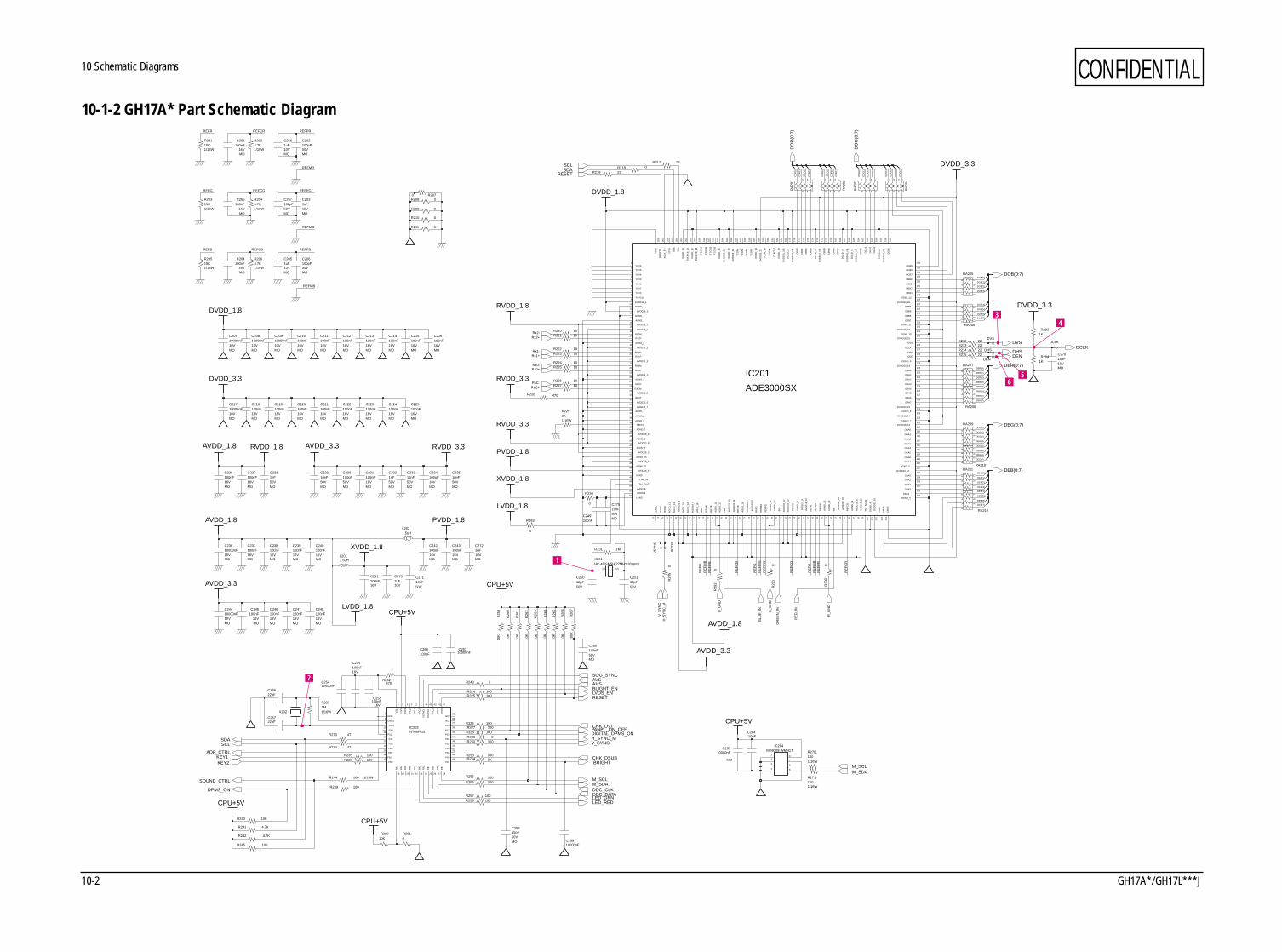
10 Schematic Diagrams
10-2 GH17A*/GH17L***J
CONFIDENTIAL10-1-2 GH17A* Part Schematic Diagram
10 Schematic Diagrams
GH17A*/GH17L***J 10-3
CONFIDENTIAL1 2 3 4 5 6
10 Schematic Diagrams
10-4 GH17A*/GH17L***J
CONFIDENTIAL
Touch Screen Option
H:NORMAL
V_sync
H_sync
L:DPMS
Seperate the Power Plane and Trace for Audio Noise
1
1
R102 100
MO10000nF
100R101
C110
1
15KR329
50V100pFC173
1/16W1.5KR146
L111L1101.5uH 1.5uH
1/16W0R335
1
50V4.7pFC103 C104
4.7pF50V
100uF25V
10KR117
C129
100nFC135
+5V
1/16W
FT101
1AB2
3
C
R1720
1
2
3
1.5uHL108
ZD
108
47R110
1
CPU+5V
CPU+5V
C116100uF25V
ZD103
1A
B2
C 3R111 0
FT103
1A 2
B
C
3
R132
1
1
10K
1.5KR190
1
CPU+5V
1/16W
1/16W100KR157
FT1111.5uH
10nFC1301uF
C147
R333
1uFC152
100
10K
R1623301/16W
R154
slcon3pCN106
123
CN102slcon7p
1
2
3
4
5
6
7
FT107BLM41P600S
1A
2B
R330
15K
1
100nFC138
1
FT1091.5uH
FT1101.5uH
1
D105
1 2
3
1
R156 10K
LCD+5V
R141
1
4.7K1/16W 1/16W
4.7K
1
R140
2
375R106
1
CPU+5V
D103
1
1
+12V_MAIN
C1611uF
1
CPU+5V
FT104BLM41P600S
1A
2B
+12V_MAIN
100R116
OUT 4
C136100nF
FAN1117AIC108
GND
1
IN3
FT106
BLM41P600S
1A
2B
L1071.5uH
2
G24
1 S1
3 S2
CPU+5V
C11810000nF
IC109SI9933ADY-T1
D18
7D1_1
D2 6
5D2_1
G1
D101
1 2
3
2
3
R113 0
1
CPU+5V
ZD107
1
100nF16V
C114
1.5uH
+12V_MAIN
AVDD_1.847uFC134
BLM41P600S
L101
100nFC133
C1511uF
1
LVDS3.3V
1
1
7
8
9
10
11
12
13
14
slcon14p_1CN104
1
2
3
4
5
6
1
1
E
1
Q1002SC2412K-Q
B
C1
680KR115
10nF
D104
1 2
3
C112
1
+5V
100nFC131
3
100nFC109
1
ZD101
1
A
B 2
C
1/16W100K
0
R138
1uFC162
CPU+5V
R173
R133
AVDD_3.3
C1501uF
1/16W10K
C140470UF16V
100nFC139
CN107dcjhp_7
1
23
VCC
+5V
MO10000nFC137
I2
9
I3
11
I4
13
I5
1
IO
4
O_1
O_2
6
8
O_3
10
O_4
12
O_5
2
O_O
14
+5V
IC114MC74F14D
7
GND
3
I1
5
50V4.7pFC105
100nFC106
100nFC108
C107 100nF
0
1
CPU+5V
R171
14
15
1
3
4
5
6
7
8
9
10
11
12
13
d_sub15pCN101
1
2
1
A
B2
C3
R103 0
DVDD_1.8
ZD102
AVDD_3.3
1uFC148
C101100pF50V
0
+12V_INVERTER
C117100nF
9
10
11
12
R105
CN108slcon12p
1
2
3
4
5
6
7
8
1
2
3
45
6
7
8
C10222pF
DVDD_3.3
GS1881-CKA
IC113 DVDD_3.3
1
CPU+5V
100nFC115
10000nFC111
2SC2412K-QQ101B
C
E
CPU+5V
10K1/16W
+12V_INVERTER
R151
Q1022SC2412K-Q
B
C
E
R112
1
4.7K1/16W
0
1
R142
C154100nF
1
C156100nF
1
D106
1 2
3
75R107
75C170100pF50VMO
A1
B2
R109
R114 100
CPU+5V
BLM41P600SFT113
BA033FPIC106
GND
IN OUT
R165
R174 100
1/16W270ohm
R1434.7K1/16W
IC112
8D1
D1_17
6D2
D2_1 5
2 G1
4 G2
S11
S23
10K1/16W
R158
SI9933ADY-T1
3 6SCL
5SDA
8VCC
VSS4
7WC_
100nFC113
24LC21AT-/SNIC101
NC_11
NC_22
NC_3
1
S2B
D11
6
C1491uF
100nFC153
2SC2412K-QQ103
B
C
E
R14410K1/16W
R176 100
R108
100R175
75
10K
100R331
47uFC132
R152
0
1/16W10KR150
R104
D102
1 2
3
C15547uF
1
0R118
1
R332100
1
FT102
A 1B2
C3
R131
1
100K1/16W
slcon2pCN105
1 2
FT112BLM41P600S
1A
2B
MC7812CD2TIC110
GND
2
IN1
OUT3
C15710000nF
R166270ohm1/16W
1/16W150R163
1
1/16W330R161
R1641501/16W
IC102BA17805FP
GND
2
1 IN 3OUT
DDC_CLK
ADP_CTRL
AVS
AHS
B_GND
R_GND
G_GND
GREEN_IN
BLUE_IN
RED_IN
R_GND
G_GND
B_GND
SOUND_CTRL
LED_GRN
LED_RED
BLIGHT_EN
RIGHT
KEY1/LEFT
EXIT
MENU
KEY2/POWER
AUTO
AUTO
RIGHT
MENU
EXITKEY1/LEFT
KEY2/POWERBRIGHT
DPMS_ON
PANEL_ON_OFF
DDC_DATA
DIGITAL_DPMS_ON
CHK_DSUB
SOG_SYNC
10-2-1 GH17L***J Part Schematic Diagram
10 Schematic Diagrams
GH17A*/GH17L***J 10-5
CONFIDENTIAL
X202
MO16V100nFC231
78
R327 100
RA207
12
34
56
C237100nF16VMO
R2070
C25015pF50V
RA211
12
34
56
78
Q0 Q1
MO50V10nFC229
HC-49/SM5H(27MHz,30ppm)
X201
3
4
5
6
7
8
5
6
7
8
RA
2041
2
RA
203 1
2
3
4
RVDD_1.8
MO16V100nFC222
XVDD_1.8
1/16W100R271
C20910000nF10VMO
C204100nF
16VMO
MO50V10nFC235
R2064.7K1/16W
MO16V100nFC243
MO16V
100nFC245
AVDD_1.8
AVDD_3.3
10K
R26
6
MO
10000nFC263
AVDD_1.8 PVDD_1.8
15K1/16W
C20710000nF10VMO
R211 0
R201
MO16V100nFC241
C240100nF16VMO
C236 C238100nF16VMO
MO16V100nFC234
MO10V10000nF
C216100nF16VMO
R274 47
C27910000nFC278
100nFC277
100nF
MO50V100pFC230
10nFC275
RA
2021
2
3
4
5
6
7
8
3
4
5
6
7
8
RA
201 1
2
MO16V100nFC224
22pF
C223100nF16VMO
C221100nF16VMO
C257
DVDD_3.3
MO16V100nFC220
RA209
12
34
56
78
MO16V100nFC215
MO16V100nFC213
LVDD_1.8
78
C212100nF16VMO
RA205
12
34
56
C210100nF16VMO
100nFC249
100R325
R270
R2831K
10000nFC253
1/16W100
100nFC268
7
8
MO16V100nFC248
M24C08-WMN1TIC204
1
2
3
4 5
6
R258 100R257
R219 22
100
100
22pF
R326
R2292K1/16W
C256
35PD0
PD134
PD233
PD332
PD431
PD530
4
RS
TB
6
V33
VS
YN
CI
44
27
PB
6
26
PB
7
25
3
PC
0
2
PC
1
1
PC
2
PC
3
42
PC
4
41
PC
5
40
PC637
36PC7
22
PA
3
21
PA
4
20
PA
5
19
PA
6
18
PA
7
17PB0
16PB1
15PB2
14PB3
PB
4
28
PB
5
38NC1
39NC2
OSCI9
OSCO8
P3010
P3111
P3412
13P35
PA029
PA
1
24
PA
2
23
AVDD_3.3
IC202NT68F63L
5
CV
V
7GND H
SY
NC
I
43
1uFC203
1.5uHL202
MO10V
R204
1/16W4.7K
VS
YN
C
R249 047R273
R239 100
0R208
1KR254
10nFC276
R255
YU
V7
208
8YUVCLK
DVDD_1.8
PVDD_1.8
100
XGND47
48XTAL_IN
XTAL_OUT49
50XVDD18
YUV07
6YUV1
YUV25
YUV34
YUV43
2YUV5
YUV61
196
195
TC
ON
3
TC
ON
419
0
189
TC
ON
5
TC
ON
618
8
187
TC
ON
7
TC
ON
_IN
184
TS
T_S
CA
N9954
VS
YN
C
205
XC
LK
XC
LK_E
N20
6
20RX1M
RX1P21
16RX2M
RX2P17
28RXCM
RXCP27
203
SC
L
SD
A20
4
TC
ON
019
8
197
TC
ON
1
TC
ON
2
64R
EF
MB
76R
EF
MG
88R
EF
MR
RE
FP
B65
RE
FP
G77
RE
FP
R8987
RE
FR
207
RE
SE
TN
30REXT
RX0M23
24RX0P
171
170
OR
B5
OR
B6
169
168
OR
B7
OVS139
36RBIAS
63R
EF
B
RE
FC
B71 83
RE
FC
G
RE
FC
R95
RE
FG
75
ORA1
ORA2131
130ORA3
ORA4129
128ORA5
ORA6127
126ORA7
177
OR
B0
176
OR
B1
OR
B2
175
174
OR
B3
OR
B4
OG
B0
163
162
OG
B1
OG
B2
161
160
OG
B3
OG
B4
157
156OGB5
155OGB6
154OGB7
OHS137
ORA0133
132
OBB7
138OCLK
136ODE
120OGA0
OGA1119
118OGA2
OGA3117
116OGA4
OGA5115
114OGA6
OGA7113
OBA4
104
OB
A5
OB
A6
103
102
OB
A7
OBB0153
152OBB1
OBB2151
OBB3150
OBB4147
146OBB5
OBB6145
144
HS
YN
C55 68
INB
80IN
G
92IN
R
52LGND
LVDD1851
OBA0110
OBA1109
108OBA2
OBA3107
106
DV
DD
18_2
2
199
DV
DD
18_2
3
201
DV
DD
18_2
4
DV
DD
33_1
610
1
DVDD33_17111
DVDD33_18125
134DVDD33_19
148DVDD33_20
158
DV
DD
33_2
1
172
DV
DD
33_2
2
185
DV
DD
33_2
3
DVDD18_13121
DVDD18_14123
140DVDD18_15
142DVDD18_16
164
DV
DD
18_1
7
166
DV
DD
18_1
8
DV
DD
18_1
917
8
DVDD18_211
180
DV
DD
18_2
0
191
DV
DD
18_2
1
193
DG
ND
_21
194
DG
ND
_22
200
DG
ND
_23
202
12DGND_3
100
DG
ND
_4
DGND_5105
DGND_6112
122DGND_7
124DGND_8
DGND_9135
DVDD18_19
143
DGND_12149
DG
ND
_13
159
DG
ND
_14
165
DG
ND
_15
167
DG
ND
_16
173
DG
ND
_17
179
DG
ND
_18
181
DG
ND
_19
186
10DGND_2
DG
ND
_20
192
AVDD33_529
AVDD33_631
32AVDD33_7
40AVDD33_8
58A
VD
D33
_9
AV
DD
_10
59
183
CLK
IN
CLK
OU
T18
2
CS
YN
C53
DGND_10141
DGND_11
85A
VD
D18
_9
AVDD33_115
AV
DD
33_1
069 70
AV
DD
33_1
1
AV
DD
33_1
281 82
AV
DD
33_1
3
AV
DD
33_1
493 94
AV
DD
33_1
5
AVDD33_219
22AVDD33_3
AVDD33_425
AVDD18_1
86A
VD
D18
_10
AV
DD
18_1
197 98
AV
DD
18_1
2
38AVDD18_2
42AVDD18_3
44AVDD18_4
46AVDD18_5
61A
VD
D18
_6
AV
DD
18_7
73 74A
VD
D18
_8
AG
ND
_21
90A
GN
D_2
2
AG
ND
_23
91 96A
GN
D_2
4
26AGND_3
AGND_433
34AGND_5
AGND_635
AGND_737
AGND_839
AGND_941
14
56A
GN
D_1
2
AG
ND
_13
57 60A
GN
D_1
4
62A
GN
D_1
5
66A
GN
D_1
6
AG
ND
_17
67 72A
GN
D_1
8
78A
GN
D_1
9
18AGND_2
AG
ND
_20
79 84
ADE3000SX
IC201
13AGND_1
AGND_1043
AGND_1145
50V10nFC271
MO16V100nFC226
6
78
C202100pF50VMO
RA208
12
34
5
RA206
12
34
56
78
RVDD_3.3
MO10V10000nFC208
100nFC211
MO16V
C239100nF16VMO
22R214
100
CPU+5V
MO16V100nFC247
R256
MO16V100nFC246
R218 22
AVDD_3.3 RVDD_3.3
16V100nFC255
MO16V100nFC218
10nFC264
C251
50V10pF
HS
YN
C
100
DHS
10K
R324
R26
010
K
R26
1
10K
R25
9
R244 100 1/16W
10000nFC259
R209 0
100R235
C2721uF10VMO
R253 100
470R232
10K
R26
5
DVDD_1.8
MO10V10000nFC217
R212 22
0R210
1/16W0R334
75R213
R2331M1/16W
10000nFC254
R230
AVDD_1.8
DVS
R26
410
K
0MO50V1nFC232
RA212
12
34
56
78
MO16V100nFC227
DEN
22
R240 10K
R215
R243 0
R241
R242 4.7K
180K
R26
7
4.7K
100R236
C2051uF10VMO
10K
R26
2
MO10V1uFC266
MO50V100pFC267
10K 1/16W
50V10nFC233
R245
RVDD_1.8
MO
0R290R292
0R291
DVDD_3.3
0
2
34
56
78
C25815pF50VMO
R284
RA210
1
1K
15K1/16W
C219100nF16VMO
MO
R205
MO16V
100nFC265
C242100nF16V
CPU+5V
0R281
R328 100
R250 100
50V15pFC270
C24410000nF10VMO
R217 22
DVDD_3.3
10KR280
R203
1/16W15K
C225100nF16VMO
10K
CPU+5V
10V1uFC273
R26
3
RVDD_3.3
R228 470
C206100pF50VMO
DCLK
1MR231
MO
CPU+5V
R2024.7K1/16W
C201100nF
16V
0R
285
1.5uHL201
XVDD_1.8
LVDD_1.8
C214100nF16VMO
C260100nF50VMO
MO50V1nFC228
SDASCL
CPU+5V
C274100nF16V
V_SYNCH_SYNC_M
CHK_DVI
LED_GRNLED_RED
M_SCLM_SDA
B_G
ND G
_GN
D
R_G
ND
SOUND_CTRL
ADP_CTRL
SOG_SYNC
BLIGHT_EN
DIGITAL_DPMS_ON
AVS
KEY2/POWERKEY1/LEFT
BRIGHT
DPMS_ON
PANEL_ON_OFF
RESET
LVDS_EN
CHK_DSUB
M_SCLM_SDA
DEN
DVS
DHSDCLK
H_S
YN
C_M
AHS
DDC_CLKDDC_DATA
DEG(3)
DEG(2)
DEG(1)
DEG(0)
DEB(3)
DEB(2)
DEB(1)
DEB(0)
DEB(7)
DEB(6)
DEB(5)
DEB(4)
DEB(0:7)
RESETSDASCL
DOB(7)
DOB(5)
DOB(6)
DER(0:7)
DER(0)
DER(1)
DER(2)
DER(3)
DER(4)
DER(5)
DER(6)
DER(7)
DEG(0:7)
DEG(7)
DEG(6)
DEG(5)
DEG(4)
DO
R(6
)
DO
R(7
)
DOG(0:7)
DO
G(0
)
DO
G(1
)
DO
G(2
)
DO
G(3
)
DO
G(4
)
DO
G(5
)
DO
G(6
)
DO
G(7
)
DOB(0:7)DOB(0)
DOB(1)
DOB(2)
DOB(3)
DOB(4)
RE
FC
G
RE
FC
R
RE
FG
RE
FM
B
RE
FM
G
RE
FM
R
RE
FP
B
RE
FP
G
RE
FP
R
RE
FR
V_S
YN
C
DOR(0:7)
DO
R(0
)
DO
R(1
)
DO
R(2
)
DO
R(3
)
DO
R(4
)
DO
R(5
)
RE
FB
RE
FC
B
BLU
E_I
N
GR
EE
N_I
N
RE
D_I
N
REFR REFCR REFPR REFMR
REFG REFCG REFPG REFMG
REFB REFCB REFPB REFMB
2
1
34
56
10-2-2 GH17L***J Part Schematic Diagram
10 Schematic Diagrams
10-6 GH17A*/GH17L***J
CONFIDENTIAL1 2 3 4 5 6
10 Schematic Diagrams
GH17A*/GH17L***J 10-7
CONFIDENTIAL
RxEC+RxE3-RxE3+
RxEC-
5V
RxE1+
Trigger Option(GND:Falling, HIGH:Rising)
5V5V
RxOC+RxO3-RxO3+
RxE0+GND
GND
RxOC-
NCNC
RxO0-
RxE0-
RxE1-
RxO0+
RxE2-RxE2+
RxO2-RxO2+GND
NC
RxO1-RxO1+
GND
47R306R305 47
A1
B2
47R304
FT304BLM41P600S
1
C30810000nF
11
1
11
1
1
C315100nF
SGM32F1E104-2AFT303
A1 2BC
3
TXOUT1+
TXOUT1-
46
41TXOUT2+
TXOUT2-
42
37TXOUT3+
TXOUT3-
38
1VCC
VCC19
26VCC2
LVDS3.3V
TXIN27
50
TXIN3
55
56TXIN4
TXIN52
TXIN63
TXIN74
TXIN86
7TXIN9
TXOUT0+47
48
TXOUT0-
45
TXIN1718
TXIN1819
TXIN1920
TXIN254
TXIN2022
TXIN2123
24TXIN22
TXIN2325
27TXIN24
TXIN2528 TXIN26
30
TXCLKOUT+
TXCLKOUT-40
TXIN0
51
52TXIN1
8TXIN10
10TXIN1111TXIN12
12TXIN13
TXIN1414
15TXIN15
TXIN1616
49
LVDSGND
LVDSGND1
43
36LVDSGND2
LVDSVCC
44
35PLLGND
PLLGND1
33
34PLLVCC
PWRDWN32
R_FB17
TXCLKIN31
39
IC301DS90C385MTD
5GND1
13
GND2
GND321
29
GND4
53GND5
LCD+5V
MO
100nFC302
SGM32F1E104-2AFT301
A 12 B
3C
C30110000nF
11
1
47R314
MO16V100nF
C306 C307C305
MO16V100nF
MO16V100nF
11
1
3C
100nFC309
LVDS3.3V
FT302SGM32F1E104-2A
1AB2
C304100nF
11
11
47R322 47R321
VCC
VCC19
26VCC2
100nFC311
TXIN7
6TXIN8
TXIN97
47
TXOUT0+
48TXOUT0-
TXOUT1+
45TXOUT1-46
TXOUT2+41
42TXOUT2-
TXOUT3+
37TXOUT3-38
1
TXIN2224
25TXIN23
27TXIN24
28TXIN25
TXIN2630
TXIN27
50
TXIN355TXIN4
56
2TXIN5
3TXIN6
4
TXIN1212TXIN13
TXIN1414
TXIN1515
TXIN1616
TXIN1718
TXIN1819
TXIN1920
54
TXIN2
22TXIN20
TXIN2123
PLLGND1
PLLVCC
34
32PWRDWN
17R_FB
TXCLKIN31
TXCLKOUT+39TXCLKOUT-40
51TXIN0
TXIN1
52
TXIN108
10TXIN11
11
GND15
GND213
GND321
29GND4
GND553
49
LVDSGND
LVDSGND1
43
LVDSGND236
44
LVDSVCC
PLLGND35
33
IC302DS90C385MTD
R317
R318 47
4747
10000nF
R316
C312100nF
LVDS3.3V
C313
R303
47
47R30847R307 1
R323 47
22
23
24
25
26
11
12
13
14
15
16
17
18
19
20
21
30
1
2
3
4
5
6
7
8
9
10
slcon30pCN301
27
28
29
47R320
1
C316
100nF
C314100uF
4747R312
R313
R311 47R310 47
47
11
R319
C303100nF
R302 10K
10KR301
100nF
R309 47
C310
1
R315 47
DOB(7)
DOB(6)
DOB(0)
DOG(5)
DOG(4)
DOG(3)
DOG(7)
DOG(6)
DOR(1)
DOR(0)
TXECLK-
TXECLK+
DCLK
DOB(0:7)
DOG(0:7)
DOR(0:7)
TXE2+
TXE1-
TXE1+
TXE0-
TXE0+
DOG(2)
DOG(1)
DOG(0)
DOR(5)
DOR(7)
DOR(4)
DOR(3)
DOR(6)
DEN
DVSDHS
DOB(5)
DOB(4)
DOB(3)
DOR(2)
DOB(2)
DOB(1)
DEB(5)
DEB(4)
DEB(3)
DER(2)
DEB(2)
DEB(1)
DEB(7)
DEB(6)
DEB(0)
DEG(5)
DEG(4)
DEG(3)
DEG(7)
DEG(6)
DER(1)
DER(0)
TXOCLK-
TXOCLK+
DEB(0:7)
DEG(0:7)
DER(0:7)
TXE3-
TXE3+
TXE2-
LVDS_EN
TXO3-
TXO3+
TXO2-
TXO2+
TXO1-
TXO1+
TXO0-
TXO0+
DEG(2)
DEG(1)
DEG(0)
DER(5)
DER(7)
DER(4)
DER(3)
DER(6)
10-3 GH17A*/GH17L***J Part Schematic Diagram
Samsung Electronics Co.,Ltd.416, Maetan-3Dong, Paldal-Gu, Suwon City, Kyungki-Do, Korea.Printed in KoreaP/N : BN82-00073C-00http://www.samsungmonitor.com (SyncMaster Worldwide)http://www.samsung-monitor.com (SyncMaster USA)http://www.sec.co.kr/monitor (Korea)