Embed Size (px)
Citation preview
Semi-Additive Process for Variant Polyimide
Substrates in Ultra-Fine Flexible Circuitry
Fei Peng, Ernest Long, Jim Watkowski, William Bowerman
■ Introduction:
Ultra-Fine and Flexible Circuitry
Semi-Additive Process (SAP)
■ SAP-FLEX for Ultra-Fine Flexible Circuitry
■ Summary
Content
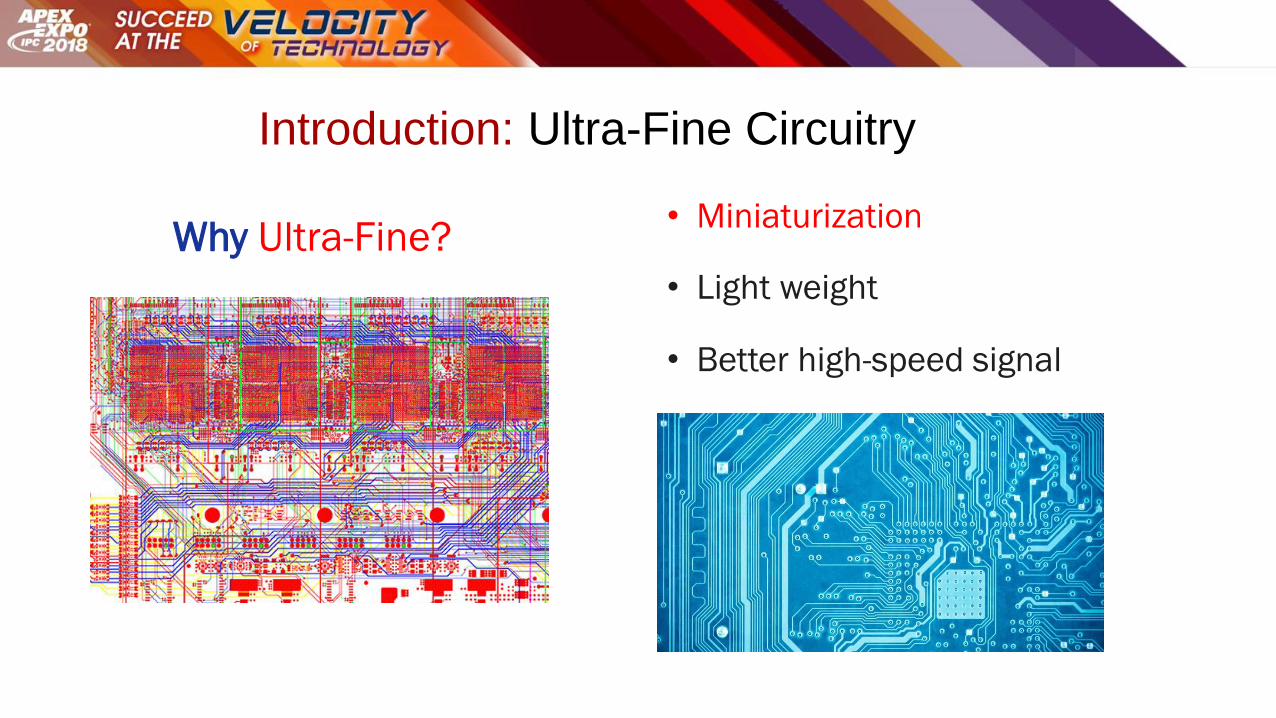
Introduction: Ultra-Fine Circuitry
Why Ultra-Fine?• Miniaturization
• Light weight
• Better high-speed signal
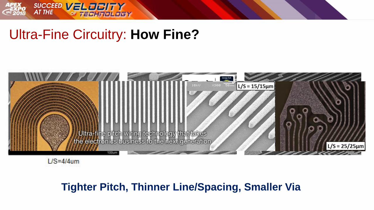
Ultra-Fine Circuitry: How Fine?
Tighter Pitch, Thinner Line/Spacing, Smaller Via
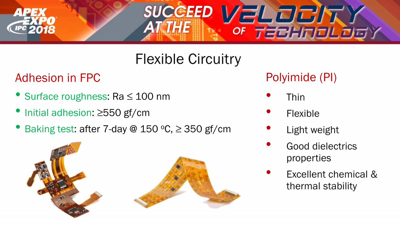
Flexible Circuitry
Polyimide (PI)
• Thin
• Flexible
• Light weight
• Good dielectrics
properties
• Excellent chemical &
thermal stability
Adhesion in FPC
• Surface roughness: Ra ≤ 100 nm
• Initial adhesion: ≥550 gf/cm
• Baking test: after 7-day @ 150 oC, ≥ 350 gf/cm
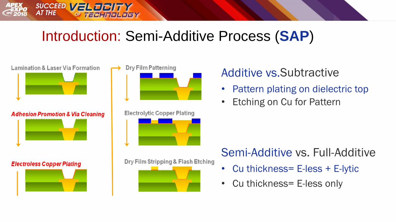
Subtractive
• Etching on Cu for Pattern
Introduction: Semi-Additive Process (SAP)
Additive vs.
• Pattern plating on dielectric top
Semi-Additive vs. Full-Additive
• Cu thickness= E-less + E-lytic
• Cu thickness= E-less only
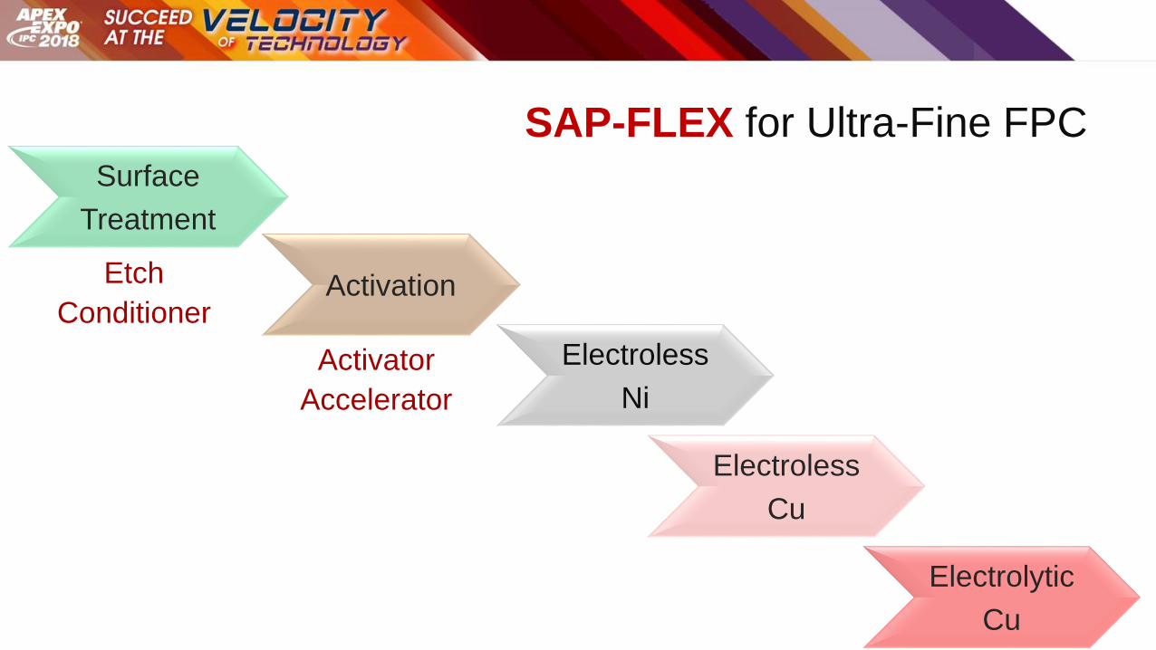
SAP-FLEX for Ultra-Fine FPCSurface
Treatment
Activation
Activator
Accelerator
Electrolytic
Cu
Electroless
Cu
Etch
Conditioner
Electroless
Ni
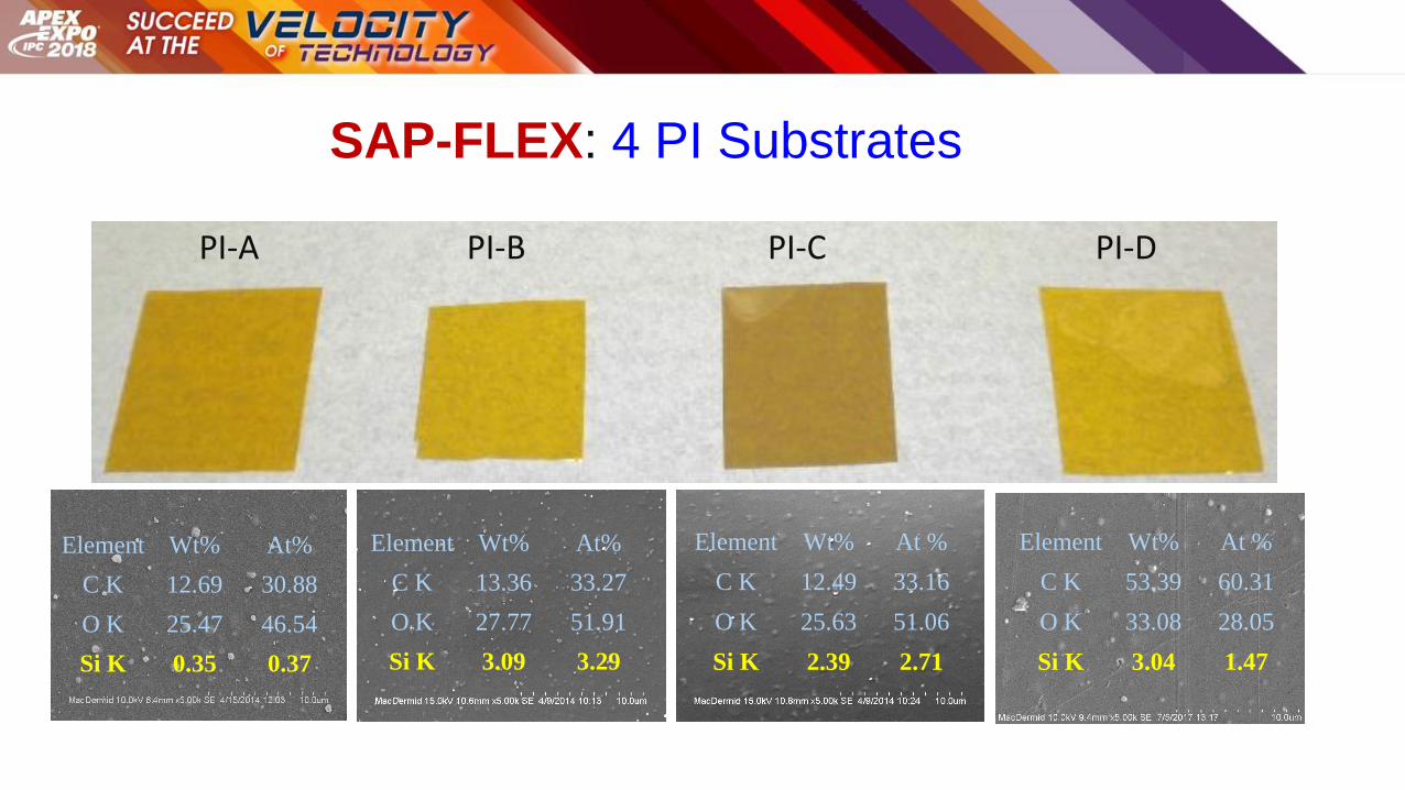
SAP-FLEX: 4 PI Substrates
PI-A PI-B PI-C PI-D
Element Wt% At%
C K 13.36 33.27
O K 27.77 51.91
Si K 3.09 3.29
Element Wt% At %
C K 12.49 33.16
O K 25.63 51.06
Si K 2.39 2.71
Element Wt% At %
C K 53.39 60.31
O K 33.08 28.05
Si K 3.04 1.47
Element Wt% At%
C K 12.69 30.88
O K 25.47 46.54
Si K 0.35 0.37
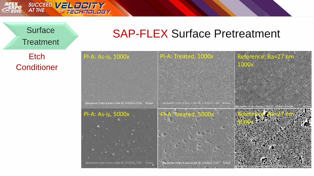
SAP-FLEX Surface PretreatmentSurface
Treatment
Etch
Conditioner
PI-A: As-is, 1000x
PI-A: As-is, 5000x
PI-A: Treated, 1000x
PI-A: Treated, 5000x
Reference: Ra=27 nm 1000x
Reference: Ra=27 nm 5000x
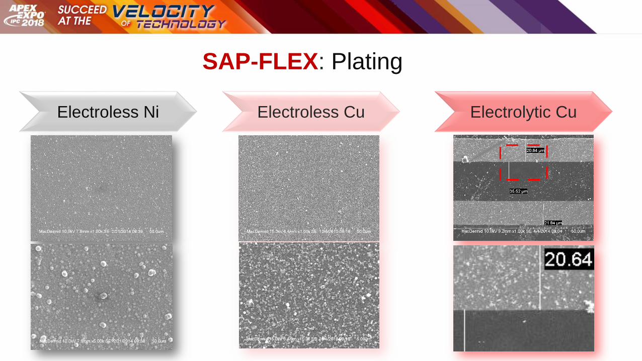
SAP-FLEX: Plating
Electroless Ni Electroless Cu Electrolytic Cu
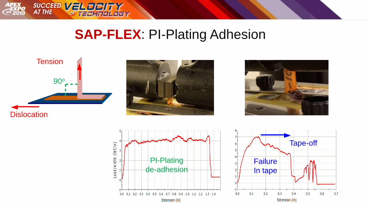
SAP-FLEX: PI-Plating Adhesion
90o
Tension
Dislocation
PI-Plating
de-adhesion
Tape-off
Failure
In tape
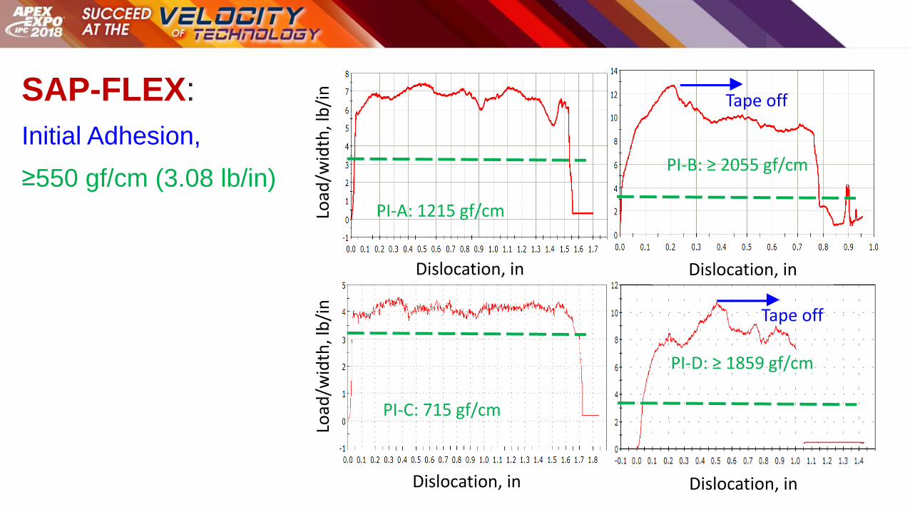
SAP-FLEX:
Initial Adhesion,
≥550 gf/cm (3.08 lb/in)
PI-D: ≥ 1859 gf/cm
PI-A: 1215 gf/cm
PI-B: ≥ 2055 gf/cm
Tape off
Tape off
Dislocation, in Dislocation, in
Load
/wid
th, l
b/i
nLo
ad/w
idth
, lb
/in
Dislocation, in
PI-C: 715 gf/cm
Dislocation, in
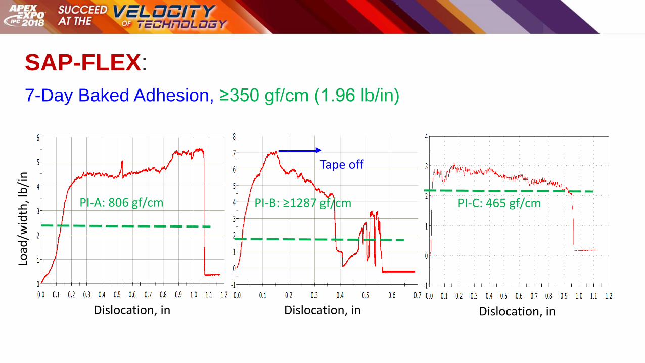
SAP-FLEX:
7-Day Baked Adhesion, ≥350 gf/cm (1.96 lb/in)
PI-A: 806 gf/cm PI-B: ≥1287 gf/cm
Tape off
Dislocation, in Dislocation, in
Load
/wid
th, l
b/i
n
Dislocation, in
PI-C: 465 gf/cm
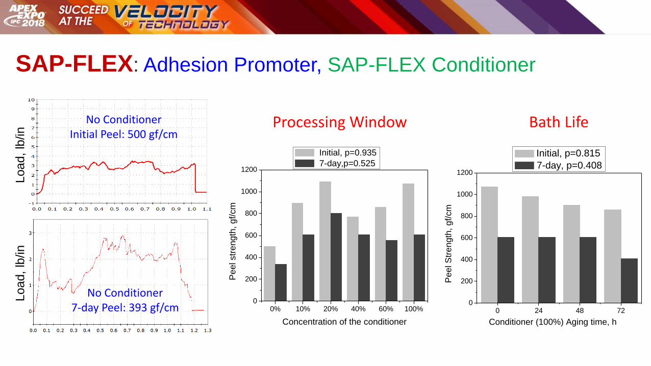
SAP-FLEX: Adhesion Promoter, SAP-FLEX Conditioner
Load,
lb/in
Load,
lb/in
No ConditionerInitial Peel: 500 gf/cm
No Conditioner7-day Peel: 393 gf/cm 0% 10% 20% 40% 60% 100%
0
200
400
600
800
1000
1200
Pe
el str
ength
, gf/cm
Concentration of the conditioner
Initial, p=0.935
7-day,p=0.525
Processing Window
0 24 48 720
200
400
600
800
1000
1200
Pee
l S
trength
, g
f/cm
Conditioner (100%) Aging time, h
Initial, p=0.815
7-day, p=0.408
Bath Life
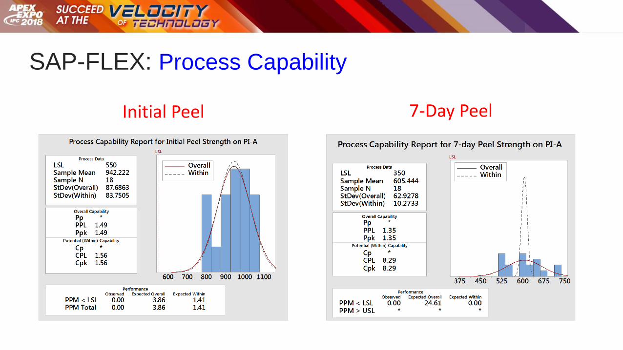
SAP-FLEX: Process Capability
Initial Peel 7-Day Peel
SAP-FLEX for Ultra-Fine Flexible Circuitry
■ Ultra smooth PI-Plating Interface
■ Excellent Chemical Bonding
■ Excellent on Different PI Substrates
■ Applies to Rigid and Flexible circuitry
16
Thank you!