Embed Size (px)
Citation preview

MPS Serial Communication Lab Exercise
Asynchronous & Synchronous Serial Communications Interface
Student's name & ID (1): ___________________________________________________
Partner's name & ID (2): ___________________________________________________
Your Section number & TA's name __________________________________________
Notes:
You must work on this assignment with your partner. Hand in a printer copy of your software listings for the team. Hand in a neat copy of your circuit schematics for the team.
These will be returned to you so that they may be used for reference.
------------------------------- do not write below this line -----------------------------
POINTS (1) (2) TA init.
Grade for performance verification (50% max.)
Part 1 (10% max.)
Part 2 (15% max.)
Part 3 (25% max.)
Enhancement (10% max)
Grade for answers to TA's questions (20% max.)
Grade for documentation and appearance (20% max.)
TOTAL
Grader's signature: ___________________________________________
Date: ______________________________________________________
Page 2
Asynchronous & Synchronous Serial Communications Interface
GOAL
By doing this lab assignment, you will learn to program and use: 1. The Asynchronous Serial Communications Ports and the Synchronous Serial Peripheral Interface. 2. Serial communications among multiple processors.
PREPARATION
• References: C8051F12x-13x.pdf 8051 C8051F12X Reference Manual, Ch. 20, 21, 22 • Write a C program that is free from syntax errors (i.e., it should assemble without error messages).
INTRODUCTION TO CONFIG2 TOOL
SiLabs provides a very useful tool that simplifies various initialization routines. Start the tool by going to the Start Menu -> Silicon Laboratories -> Configuration Wizard 2. On the File menu, click New to create a new project. Under Select Device Family select C8051F12x, and then select C8051F120. This tool will produce a header file for you that will have all of the initialization routines for the various subsystems (UART, SPI, etc). Of main interest are all of the items under the Peripherals menu. For example, you may want to use the Config2 tool to create your SPI initialization function. Click on Peripherals -> SPI and a new window will open. Here, you can enable SPI, set polarity, enable interrupts, and more. Also, the Config2 tool provides a very convenient way to enable things in the crossbar. By clicking on Peripherals -> Port I/O the Config2 will bring up the crossbar configuration window. Here, you can enable various systems such as UART0, and set pins to open drain/push-pull (along the bottom of the window).
NOTE: While this tool simplifies and speeds up the development process, you should still have a thorough understanding of all the registers that you modify. To show this understanding, you will need to describe your reasoning behind the way you set up all of the registers used through the Config2 tool in your lab write-up.
UNIVERSAL ASYNCHRONOUS RECEIVER TRANSMITTER (UART)
1. Introduction To The Asynchronous Serial Communications Port
The 8051 has two on-board universal asynchronous receiver/transmitter interfaces, UART0 and UART1, and an additional synchronous serial peripheral interface, SPI0. The C8051F120 board has one built-in RS-232 port which UART0 or UART1 may be configured to use. The UARTs can be configured through the SFR registers listed below.
SCONn: Control register to set UART0 mode, reception, and interrupt flags
SBUFn: UART0 data buffer. Moving data to this register initiates transmission
SSTA0 : Control register for advanced features such as detecting framing errors, transmit collisions, and receive overrun and setting the corresponding flags (There is no SSTA1.)
In more sophisticated configurations, interrupts may be generated when data is received or ready to be transmitted and when transmission, framing or overrun errors are detected. Self-checking modes may
Page 3
also be configured and auto wakeup sequences employed.
2. Asynchronous Serial Port Setup
In the basic mode, a three-step set-up sequence is all that is necessary. First, the port must be enabled for transmitting and receiving. Second, the number of data bits chosen (the C8051 does not provide for parity checking or for 2 stop bits) - the standard RS-232 parameters. Finally, the baud rate must be selected. The chip is extremely flexible in allowing the selection of all standard rates as well as custom rates. Table 21.2 on page 295 of the C8051F120 manual shows a few possible baud rates and the timer reset values needed to achieve the desired baud rate. Remember that the C8051F120 board has a system clock frequency of 22.1184MHz.
Transmitting a character through a port involves a simple two-step procedure. First the Transmit Interrupt (TIn) Flag must be checked to see that it is set. If not, the program must wait and keep checking until the bit is high. Then the data to be transmitted must be loaded into the Data Buffer (SBUFn). Receiving data is a similar two-step process. The Receive Interrupt (RIn) Flag must be checked. If it is cleared, this indicates that no data is available and the program may go on to something else or decide to wait for something to appear by repeatedly checking the flag. A set flag indicates that data is available and may be read from the Data Buffer. Note that the same data register is used for transmitting as well as receiving data. If the UART is set up to transmit and receive data in interrupt mode, the TIn and RIn flags need to be reset by the interrupt routine. If the UART is operated in polled mode, the flags will be reset automatically when a read/write is performed on SBUFn.
SYNCHRONOUS SERIAL PORT
1. Synchronous Serial Port Interface (SPI) Setup
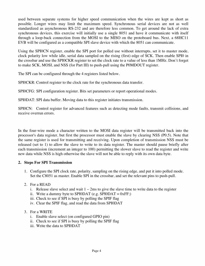
Synchronous serial communication between processors is possible using the Synchronous Serial Peripheral Interface (SPI0) port on the 8051. Synchronous, or separately clocked, serial connections can communicate at much higher rates than standard RS-232 data rates. They also use master/slave configurations between devices where the single master provides the clocking signal to all slave devices. The figure below shows the signals between two SPI devices and also demonstrates the mechanism where, as data from one device is clocked out of its shift register, data from the second device is simultaneously clocked into the register.
SPI is designed as a short-range, on-board bus specification for distances of less than a foot, it may be
Page 4
used between separate systems for higher speed communication when the wires are kept as short as possible. Longer wires may limit the maximum speed. Synchronous serial devices are not as well standardized as asynchronous RS-232 and are therefore less common. To get around the lack of extra synchronous devices, this exercise will initially use a single 8051 and have it communicate with itself through a loop-back connection from the MOSI to the MISO on the protoboard bus. Next, a 68HC11 EVB will be configured as a compatible SPI slave device with which the 8051 can communicate.
Using the SPI0CN register, enable the SPI port for polled use without interrupts, set it to master mode, clock polarity low while idle, serial data sampled on the rising (first) edge of SCK. Then enable SPI0 in the crossbar and use the SPI0CKR register to set the clock rate to a value of less than 1MHz. Don’t forget to make SCK, MOSI, and NSS (for Part III) to push-pull using the P0MDOUT register.
The SPI can be configured through the 4 registers listed below.
SPI0CKR: Control register to the clock rate for the synchronous data transfer.
SPI0CFG: SPI configuration register. Bits set parameters or report operational modes.
SPI0DAT: SPI data buffer. Moving data to this register initiates transmission.
SPI0CN: Control register for advanced features such as detecting mode faults, transmit collisions, and receive overrun errors.
In the four-wire mode a character written to the MOSI data register will be transmitted back into the processor's data register, but first the processor must enable the slave by clearing NSS (P0.5). Note that the same register is used for transmitting and receiving. Upon completion of transmission NSS must be released (set to 1) to allow the slave to write to its data register. The master should pause briefly after each transmission (increment an integer to 100) permitting the slower slave to read the register and write new data while NSS is high otherwise the slave will not be able to reply with its own data byte.
2. Steps For SPI Transmission
1. Configure the SPI clock rate, polarity, sampling on the rising edge, and put it into polled mode. Set the C8051 as master. Enable SPI in the crossbar, and set the relevant pins to push-pull.
2. For a READ i. Release slave select and wait 1 – 2ms to give the slave time to write data to the register ii. Write a dummy byte to SPI0DAT (e.g. SPI0DAT = 0xFF;) iii. Check to see if SPI is busy by polling the SPIF flag iv. Clear the SPIF flag, and read the data from SPI0DAT
3. For a WRITE i. Enable slave select (on configured GPIO pin) ii. Check to see if SPI is busy by polling the SPIF flag iii. Write the data to SPI0DAT
Page 5
PROGRAMMING TASKS
PART I
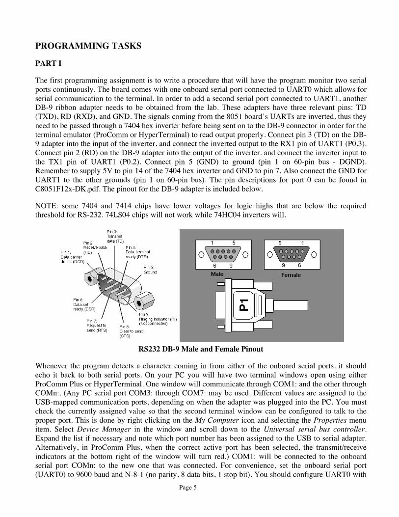
The first programming assignment is to write a procedure that will have the program monitor two serial ports continuously. The board comes with one onboard serial port connected to UART0 which allows for serial communication to the terminal. In order to add a second serial port connected to UART1, another DB-9 ribbon adapter needs to be obtained from the lab. These adapters have three relevant pins: TD (TXD), RD (RXD), and GND. The signals coming from the 8051 board’s UARTs are inverted, thus they need to be passed through a 7404 hex inverter before being sent on to the DB-9 connector in order for the terminal emulator (ProComm or HyperTerminal) to read output properly. Connect pin 3 (TD) on the DB-9 adapter into the input of the inverter, and connect the inverted output to the RX1 pin of UART1 (P0.3). Connect pin 2 (RD) on the DB-9 adapter into the output of the inverter, and connect the inverter input to the TX1 pin of UART1 (P0.2). Connect pin 5 (GND) to ground (pin 1 on 60-pin bus - DGND). Remember to supply 5V to pin 14 of the 7404 hex inverter and GND to pin 7. Also connect the GND for UART1 to the other grounds (pin 1 on 60-pin bus). The pin descriptions for port 0 can be found in C8051F12x-DK.pdf. The pinout for the DB-9 adapter is included below.
NOTE: some 7404 and 7414 chips have lower voltages for logic highs that are below the required threshold for RS-232. 74LS04 chips will not work while 74HC04 inverters will.
RS232 DB-9 Male and Female Pinout
Whenever the program detects a character coming in from either of the onboard serial ports, it should echo it back to both serial ports. On your PC you will have two terminal windows open using either ProComm Plus or HyperTerminal. One window will communicate through COM1: and the other through COMn:. (Any PC serial port COM3: through COM7: may be used. Different values are assigned to the USB-mapped communication ports, depending on when the adapter was plugged into the PC. You must check the currently assigned value so that the second terminal window can be configured to talk to the proper port. This is done by right clicking on the My Computer icon and selecting the Properties menu item. Select Device Manager in the window and scroll down to the Universal serial bus controller. Expand the list if necessary and note which port number has been assigned to the USB to serial adapter. Alternatively, in ProComm Plus, when the correct active port has been selected, the transmit/receive indicators at the bottom right of the window will turn red.) COM1: will be connected to the onboard serial port COMn: to the new one that was connected. For convenience, set the onboard serial port (UART0) to 9600 baud and N-8-1 (no parity, 8 data bits, 1 stop bit). You should configure UART0 with
Page 6
Timer2. Use the equations on page 290 (Eq. 21.3 & 21.4) or Table 21.2 in C8051F12x-13x.pdf to determine the baud rate for UART0.
UART1 must be configured with Timer1 (mode 2) for 115200 baud and N-8-1. Use the tables on pages 305-307 in C8051F12x-13x.pdf to determine the baud rate settings for UART1, depending on what system clock is selected (external clock 22.1184MHz is recommended). You will need to configure it manually as well as send and receive characters using the status, control, and data registers. Remember you must match the terminal program’s setup parameters to the port's configuration. Note that the PCs support only COM1: directly. COMn: is created by using a USB to Serial converter and software that allows the USB port and hardware to emulate a second serial port on the PC. There is a typo on p. 300 of the manual revision 1.4. T1H in Eq. 22.1 should be TH1.
Write a program to poll both ports continuously and then echo any character received to both ports so the received character will show up on both displays. An <ESC> key pressed on the onboard serial port (UART0) should display a brief message on both screens and halt the program. Note that getch() can’t be used for polling because the function will just wait for UART0 to receive a character.
Helpful Hint:
Test your hardware wiring first. Besides being connected to the on-board DB-9 connector, UART0’s TX and RX pins can also be found on P0.0 and P0.1. Connect your hardware to these pins first, and make sure that your second DB-9 connector is working before writing any code to configure UART1. You must first disable the on-board DB-9 connection by pulling jumpers J6 & J9. You can test the second DB-9 connector by running a program from any of the previous labs with output to UART0. Once verifying that your hardware wiring is correct, write your code to enable UART1. This will help isolate your debugging to software-only problems. Also, with UART0 disabled and only UART1 enabled (J6 & J9 replaced) UART1 will use the on-board DB-9 connector to help in troubleshooting. If UART0 is disabled all functions using it must be disabled to keep your program from locking up. If available, jumpers fitting on the J6 & J9 pins that can be moved between P0.0, P0.1 and P0.2, P0.3 will permit both UARTs to be enabled simultaneously and have one or the other use the DB-9. Remember to set the terminal BAUD rate correctly for each UART. 1. Enabling UART0 and UART1 on the crossbar does not automatically set the correct pins to outputs
and inputs. You must configure both TX pins to push-pull and both RX pins to open-drain and put the open-drain pins in high impedance mode. You can get some very strange behaviors if this is not done, where it may work on one PC terminal program but not on a different PC and many characters will be corrupted.
2. If you use a DB-9 converter (male to male or female to female), make sure the pin numbering is correct.
3. The pin layout for port 0 on the EVB board should be marked to indicate where pin 1, 2, etc. are located; if not, check another board for locations.
4. If RTS (DB-9, pin 7) is connected by mistake, the terminal will not output characters. 5. If the incorrect baud rate is configured, the terminal will not output characters or the terminal will
output seemingly random characters. 6. If GND was connected to pin 1 instead of pin 5 on the DB-9, the terminal will output abnormal
characters. 7. If GND, RXD, TXD are disconnected or if RXD and TXD are switched on the DB-9, the terminal
will not output characters. 8. If numerous random characters are repeatedly sent and echoed to the terminals, insure that the
grounds on pin 1 (60-pin bus) and the protoboard are tied together. The pin descriptions can be found
Page 7
on table 5 in C8051F12x-DK.pdf. 9. The code does not need to be downloaded every time after halting; only when software changes are
made. The reset button on the board will restart the program. 10. When configuring RI0, the SDCC compiler will give an unidentified error. You do not need to
configure RI0. 11. Must set keyboard input (i.e. choice in hello.c) = SBUFn initially rather than SBUFn = choice.
PART II
This program duplicates the functionality of the program in Part I but allows the serial ports to generate interrupts when characters are received and has ISRs handle the job of echoing the received characters to the two displays. Interrupt 4 is assigned to UART0 and 20 to UART1. The assignment of interrupts to ISRs follows the same convention as was used in the Interrupts and Timer ISRs lab exercise. Note that each interrupt (4 or 20) is shared by several causes on the port including a receive or transmit. This means that the ISRs must interrogate the TIn and RIn bits in the SCONn registers to find the particular cause of a generated interrupt and take appropriate action for each separate cause. The main objective of this exercise is to handle the receive interrupt but you may choose to write code to handle other cases, including framing and parity errors.
When you have completed the program and verified its operation, you will need to find another group with a working version of Part II and connect your two serial ports together via the TX1 & RX1 signals and a common ground. Remember transmit on one processor must be connected to receive on the other processor. When connecting the TX1 & RX1 signals you should bypass the inverters that were used in Part I when UART1 was connected to the true RS232 DB-9 input on the PC. Now any character typed on the UART0 terminal on either processor will show up on the other processor's terminal.
Helpful Hint:
1. Use the following code to configure the receive interrupt:
while(!RI1) // Receive interrupt flag { SFRPAGE = UART0_PAGE; // Direct output to UART0 if(!RI1)
{ SFRPAGE = UART1_PAGE; // Direct output to UART1 } } RI1 = 0; // Receive interrupt flag cleared
2. Use while(!TI0);
when configuring the transmit interrupt flag as the while loop rather than
while(!TI0){ }.
NOTE: An unexpected consequence of using interrupts in Part II is that UART1 may seem to be unable to transmit characters. Following the normal sequence of waiting for the receive flag to be set before reading from the UART buffer, and making sure the transmit flag is set before loading the buffer with the
Page 8
character to be sent causes problems. After completing a transmission, the transmit flag is always high and as a result, the ISR for a UART is executed continuously. With nothing to transmit most of the time, as soon as the ISR is finished, it is immediately called again since the transmit flag is still set. With UART0 at a higher priority than UART1, the ISR for UART1 is never executed, even though its receive (and transmit) flag may be set. The workaround for this dilemma is to disable the interrupt for UART0 briefly during each cycle to give the ISR for 1 a chance to execute when a character is received on UART1. A messy alternative is to clear the transmit ready flags and somehow be able to distinguish between when the flags were cleared by software and when they were cleared by hardware during the transmission of characters. Ideally it would be great if the ISRs could only execute on a receive flag!
PART III
Write a simple C program to set up and communicate through the 8051’s SPI. Initially the port will only talk to itself through a wire connecting MOSI to MISO. Any character transmitted will be the same character received while the loop-back wire is present. If the input to MISO is held to ground or +5 volts, the input character should be 0x00 or 0xFF respectively after a transmission is received (Why?). Use your program to verify all three cases. Write your program so that it uses ANSI escape sequences to split the terminal window in half with the top half used to display characters typed locally at the keyboard to be sent out the SPI port and the bottom half to display characters received by the SPI serial port. It is not necessary to scroll the top half and bottom half separately as the number of lines hits the limit of half the screen, but doing so will enhance your grade. After verifying operation with the simple loop-back connection, the next part of the procedure is to incorporate a second EVB, a 68HC11, as a slave SPI device. A program called SPISLAVE is available for your use on the course web page to run on the HC11, allowing it to send and receive synchronous serial data in slave mode. The 68HC11 EVB with the provided software will permit you to verify your program with more interesting test strings under more realistic operating conditions. When running with the loop-back wire, SPI clock frequencies of 1 to 4 MHz should work, but when connecting to the slower HC11 EVB through the EVB bus protection circuits to the protoboard, these may need to be reduced to 1 MHz (the HC11’s maximum speed) or less. The combination of loose unshielded wires, ribbon cables, and bus buffers in both directions make this change necessary. Additionally, with the direct loop-back wire, transmitted data will be received instantly while when going through a slave device, the reply will be delayed by one character transmission due to the added second shift register in the slave. Your software will need to accommodate this circumstance.
SPISLAVE.C is a program for the HC11 EVB that will configure its synchronous SPI serial port to run as a slave device. The S19 file is available on the class WebCT site under Course Handouts and may also be in the HC11 directory under CStudio on the studio PCs. This program is designed to accept characters clocked in from an SPI master device on one transfer and echo back the same character on the following transfer. The slave will display the transmitted character on its console when it has been received. This can be used as an aid in debugging. An additional feature on the slave may be implemented in the downloaded S19 version. This function will transmit a message from the slave to the master when the master sends a <DEL> character (0x7F). Upon receipt of a <DEL>, the slave still echoes it back on the following transfer as with all characters, but follows this with a sequence of printable ASCII characters in a string sent to the master ending with a 0xFF character (about 100 character total). The master must transmit dummy characters to the slave until the 0xFF is received in order to obtain the entire message.
Use the following commands to download the program to the HC11 EVB through a ProComm Plus connection directly to the serial port (0) at 9600 baud on the EVB. Make sure the ProComm terminal is in ANSI BBS mode and the Xfer protocol is ASCII or RAW ASCII (lower left corner, 2nd line up).
Page 9
Hit <Enter> once or twice L T<Enter> (click on the Send File icon at the top and then select the SPISLAVE.S19 file) G 6000<Enter> (begin execution)
If HyperTerminal is used instead of ProComm Plus, set Connect using: to COM1, and under Configure… make sure to use 9600 Bits per second, 8 Data bits, no Parity (None), 1 Stop bit, and Xon/Xoff for Flow control. Then after the L T<Enter> command, select Transfer → Send Text File… to download the desired .S19 file.
When SPISLAVE is executed on the HC11 EVB it displays on its console hardware configuration data for wiring up the HC11 to the 8051. If SPISLAVE does not seem to be functioning correctly, try restarting it (reloading it is not necessary after a simple reset) after starting your SPI master program on the 8051.
DETAILS
The source code for SPISLAVE is available on the course web page. For those interested in how it works, here is a little bit of background information on how the registers are used to configure the SPI operations.
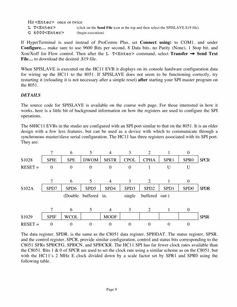
The 68HC11 EVBs in the studio are configured with an SPI port similar to that on the 8051. It is an older design with a few less features, but can be used as a device with which to communicate through a synchronous master/slave serial configuration. The HC11 has three registers associated with its SPI port. They are:
7 6 5 4 3 2 1 0 $1028 SPIE SPE DWOM MSTR CPOL CPHA SPR1 SPR0 SPCR RESET = 0 0 0 0 0 1 U U 7 6 5 4 3 2 1 0 $102A SPD7 SPD6 SPD5 SPD4 SPD3 SPD2 SPD1 SPD0 SPDR (Double buffered in, single buffered out ) 7 6 5 4 3 2 1 0 $1029 SPIF WCOL MODF SPSR RESET = 0 0 0 0 0 0 0 0
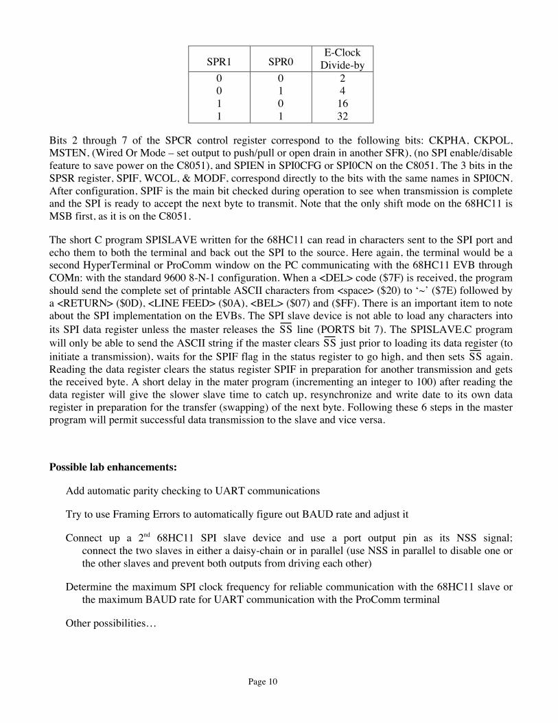
The data register, SPDR, is the same as the C8051 data register, SPI0DAT. The status register, SPSR, and the control register, SPCR, provide similar configuration, control and status bits corresponding to the C8051 SFRs SPI0CFG, SPI0CN, and SPI0CKR. The HC11 SPI has far fewer clock rates available than the C8051. Bits 1 & 0 of SPCR are used to set the clock rate using a similar scheme as on the C8051, but with the HC11’s 2 MHz E clock divided down by a scale factor set by SPR1 and SPR0 using the following table.
Page 10
SPR1 SPR0 E-Clock
Divide-by 0 0 1 1
0 1 0 1
2 4 16 32
Bits 2 through 7 of the SPCR control register correspond to the following bits: CKPHA, CKPOL, MSTEN, (Wired Or Mode – set output to push/pull or open drain in another SFR), (no SPI enable/disable feature to save power on the C8051), and SPIEN in SPI0CFG or SPI0CN on the C8051. The 3 bits in the SPSR register, SPIF, WCOL, & MODF, correspond directly to the bits with the same names in SPI0CN. After configuration, SPIF is the main bit checked during operation to see when transmission is complete and the SPI is ready to accept the next byte to transmit. Note that the only shift mode on the 68HC11 is MSB first, as it is on the C8051.
The short C program SPISLAVE written for the 68HC11 can read in characters sent to the SPI port and echo them to both the terminal and back out the SPI to the source. Here again, the terminal would be a second HyperTerminal or ProComm window on the PC communicating with the 68HC11 EVB through COMn: with the standard 9600 8-N-1 configuration. When a <DEL> code ($7F) is received, the program should send the complete set of printable ASCII characters from <space> ($20) to ‘~’ ($7E) followed by a <RETURN> ($0D), <LINE FEED> ($0A), <BEL> ($07) and ($FF). There is an important item to note about the SPI implementation on the EVBs. The SPI slave device is not able to load any characters into its SPI data register unless the master releases the SS line (PORTS bit 7). The SPISLAVE.C program will only be able to send the ASCII string if the master clears SS just prior to loading its data register (to initiate a transmission), waits for the SPIF flag in the status register to go high, and then sets SS again. Reading the data register clears the status register SPIF in preparation for another transmission and gets the received byte. A short delay in the mater program (incrementing an integer to 100) after reading the data register will give the slower slave time to catch up, resynchronize and write date to its own data register in preparation for the transfer (swapping) of the next byte. Following these 6 steps in the master program will permit successful data transmission to the slave and vice versa.
Possible lab enhancements:
Add automatic parity checking to UART communications
Try to use Framing Errors to automatically figure out BAUD rate and adjust it
Connect up a 2nd 68HC11 SPI slave device and use a port output pin as its NSS signal; connect the two slaves in either a daisy-chain or in parallel (use NSS in parallel to disable one or the other slaves and prevent both outputs from driving each other)
Determine the maximum SPI clock frequency for reliable communication with the 68HC11 slave or the maximum BAUD rate for UART communication with the ProComm terminal
Other possibilities…