Embed Size (px)
Citation preview
Rev 1.2 12/15 Copyright © 2015 by Silicon Laboratories Si52112-B5/B6
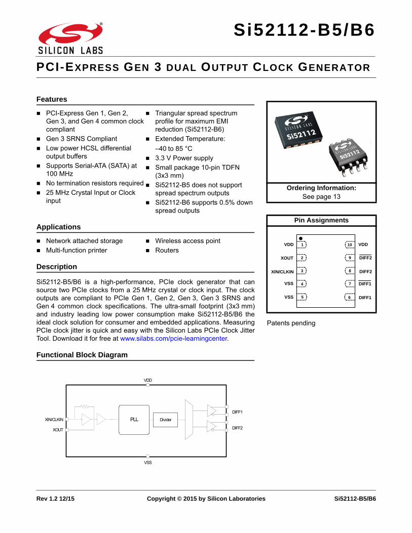
Si52112-B5/B6
PCI-EXPRESS GEN 3 DUAL OUTPUT CLOCK GENERATOR
Features
Applications
Description
Si52112-B5/B6 is a high-performance, PCIe clock generator that cansource two PCIe clocks from a 25 MHz crystal or clock input. The clockoutputs are compliant to PCIe Gen 1, Gen 2, Gen 3, Gen 3 SRNS andGen 4 common clock specifications. The ultra-small footprint (3x3 mm)and industry leading low power consumption make Si52112-B5/B6 theideal clock solution for consumer and embedded applications. MeasuringPCIe clock jitter is quick and easy with the Silicon Labs PCIe Clock JitterTool. Download it for free at www.silabs.com/pcie-learningcenter.
Functional Block Diagram
PCI-Express Gen 1, Gen 2, Gen 3, and Gen 4 common clock compliant
Gen 3 SRNS Compliant
Low power HCSL differential output buffers
Supports Serial-ATA (SATA) at 100 MHz
No termination resistors required
25 MHz Crystal Input or Clock input
Triangular spread spectrum profile for maximum EMI reduction (Si52112-B6)
Extended Temperature:
–40 to 85 °C
3.3 V Power supply
Small package 10-pin TDFN (3x3 mm)
Si52112-B5 does not support spread spectrum outputs
Si52112-B6 supports 0.5% down spread outputs
Network attached storage
Multi-function printer
Wireless access point
Routers
XIN/CLKIN
XOUT DIFF2
DIFF1
PLL Divider
VDD
VSS
Patents pending
Ordering Information:See page 13
Pin Assignments
10
9
8
7
1
2
3
4
VDDVDD
XOUT
XIN/CLKIN
VSS
VSS 5 6 DIFF1
DIFF1
DIFF2
DIFF2
Si52112-B5/B6
2 Rev 1.2
Si52112-B5/B6
Rev 1.2 3
TABLE OF CONTENTS
Section Page
1. Electrical Specifications . . . . . . . . . . . . . . . . . . . . . . . . . . . . . . . . . . . . . . . . . . . . . . . . . . . . . . . . . 42. Crystal Recommendations . . . . . . . . . . . . . . . . . . . . . . . . . . . . . . . . . . . . . . . . . . . . . . . . . . . . . . . 7
2.1. Crystal Loading . . . . . . . . . . . . . . . . . . . . . . . . . . . . . . . . . . . . . . . . . . . . . . . . . . . . . . . . . . . . 72.2. Calculating Load Capacitors . . . . . . . . . . . . . . . . . . . . . . . . . . . . . . . . . . . . . . . . . . . . . . . . . . 8
3. Test and Measurement Setup . . . . . . . . . . . . . . . . . . . . . . . . . . . . . . . . . . . . . . . . . . . . . . . . . . . . . 94. Pin Descriptions . . . . . . . . . . . . . . . . . . . . . . . . . . . . . . . . . . . . . . . . . . . . . . . . . . . . . . . . . . . . . . . 11
4.1. 10-Pin TDFN . . . . . . . . . . . . . . . . . . . . . . . . . . . . . . . . . . . . . . . . . . . . . . . . . . . . . . . . . . . . . 114.2. 8-Pin TSSOP . . . . . . . . . . . . . . . . . . . . . . . . . . . . . . . . . . . . . . . . . . . . . . . . . . . . . . . . . . . . 12
5. Ordering Guide . . . . . . . . . . . . . . . . . . . . . . . . . . . . . . . . . . . . . . . . . . . . . . . . . . . . . . . . . . . . . . . . 136. Package Outlines . . . . . . . . . . . . . . . . . . . . . . . . . . . . . . . . . . . . . . . . . . . . . . . . . . . . . . . . . . . . . . 14
6.1. TDFN Package . . . . . . . . . . . . . . . . . . . . . . . . . . . . . . . . . . . . . . . . . . . . . . . . . . . . . . . . . . . 146.2. TSSOP Package . . . . . . . . . . . . . . . . . . . . . . . . . . . . . . . . . . . . . . . . . . . . . . . . . . . . . . . . . . 16
7. Recommended Design Guideline . . . . . . . . . . . . . . . . . . . . . . . . . . . . . . . . . . . . . . . . . . . . . . . . . 18Document Change List . . . . . . . . . . . . . . . . . . . . . . . . . . . . . . . . . . . . . . . . . . . . . . . . . . . . . . . . . . . . 19
Si52112-B5/B6
4 Rev 1.2
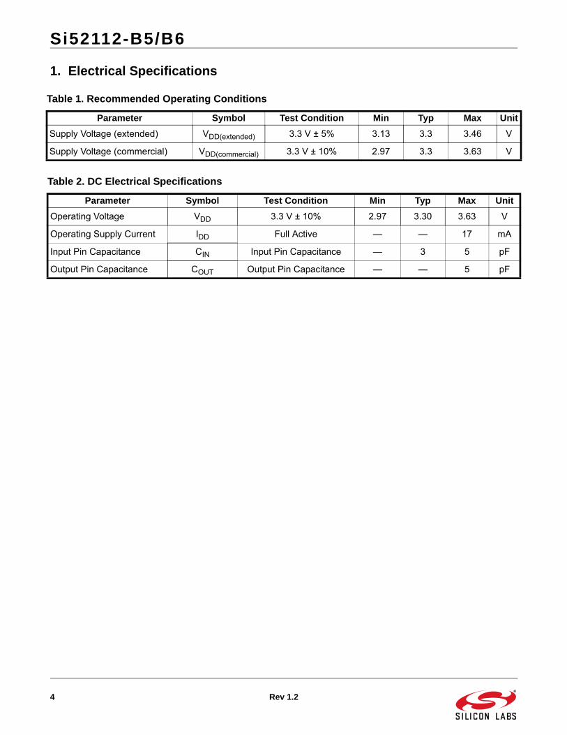
1. Electrical Specifications
Table 1. Recommended Operating Conditions
Parameter Symbol Test Condition Min Typ Max Unit
Supply Voltage (extended) VDD(extended) 3.3 V ± 5% 3.13 3.3 3.46 V
Supply Voltage (commercial) VDD(commercial) 3.3 V ± 10% 2.97 3.3 3.63 V
Table 2. DC Electrical Specifications
Parameter Symbol Test Condition Min Typ Max Unit
Operating Voltage VDD 3.3 V ± 10% 2.97 3.30 3.63 V
Operating Supply Current IDD Full Active — — 17 mA
Input Pin Capacitance CIN Input Pin Capacitance — 3 5 pF
Output Pin Capacitance COUT Output Pin Capacitance — — 5 pF
Si52112-B5/B6
Rev 1.2 5
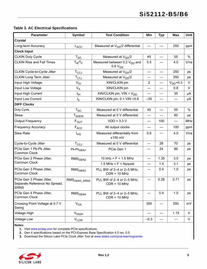
Table 3. AC Electrical Specifications
Parameter Symbol Test Condition Min Typ Max Unit
Crystal
Long-term Accuracy LACC Measured at VDD/2 differential — — 250 ppm
Clock Input
CLKIN Duty Cycle TDC Measured at VDD/2 45 — 55 %
CLKIN Rise and Fall Times TR/TF Measured between 0.2 VDD and 0.8 VDD
0.5 — 4.0 V/ns
CLKIN Cycle-to-Cycle Jitter TCCJ Measured at VDD/2 — — 250 ps
CLKIN Long Term Jitter TLTJ Measured at VDD/2 — — 350 ps
Input High Voltage VIH XIN/CLKIN pin 2 — VDD+0.3 V
Input Low Voltage VIL XIN/CLKIN pin — — 0.8 V
Input High Current IIH XIN/CLKIN pin, VIN = VDD — — 35 µA
Input Low Current IIL XIN/CLKIN pin, 0 < VIN <0.8 –35 — — µA
DIFF Clocks
Duty Cycle TDC Measured at 0 V differential 45 — 55 %
Skew TSKEW Measured at 0 V differential — — 60 ps
Output Frequency FOUT VDD = 3.3 V — 100 — MHz
Frequency Accuracy FACC All output clocks — — 100 ppm
Slew Rate tr/f2 Measured differentially from ±150 mV
0.6 — 4.0 V/ns
Cycle-to-Cycle Jitter TCCJ Measured at 0 V differential — 28 70 ps
PCIe Gen 1 Pk-Pk Jitter, Common Clock
Pk-PkGEN1 PCIe Gen 1 — 24 86 ps
PCIe Gen 2 Phase Jitter, Common Clock
RMSGEN2 10 kHz < F < 1.5 MHz — 1.35 3.0 ps
1.5 MHz < F < Nyquist — 1.4 3.1 ps
PCIe Gen 3 Phase Jitter, Common Clock
RMSGEN3 PLL BW of 2–4 or 2–5 MHz,CDR = 10 MHz
— 0.4 1.0 ps
PCIe Gen 3 Phase Jitter, Separate Reference No Spread, SRNS
RMSGEN3_SRNS PLL BW of 2–4 or 2–5 MHz,CDR = 10 MHz
— 0.28 0.71 ps
PCIe Gen 4 Phase Jitter, Common Clock
RMSGEN4 PLL BW of 2–4 or 2–5 MHz,CDR = 10 MHz
— 0.4 1.0 ps
Crossing Point Voltage at 0.7 V Swing
VOX 300 — 550 mV
Voltage High VHIGH — — 1.15 V
Voltage Low VLOW –0.3 — — V
Notes:1. Visit www.pcisig.com for complete PCIe specifications.2. Gen 4 specifications based on the PCI-Express Base Specification 4.0 rev. 0.5.3. Download the Silicon Labs PCIe Clock Jitter Tool at www.silabs.com/pcie-learningcenter.
Si52112-B5/B6
6 Rev 1.2
Spread Range SRNG Down Spread, -B6 only — –0.5 — %
Modulation Frequency FMOD -B6 only 30 31.5 33 kHz
Enable/Disable and Set-up
Clock Stabilization from Power-up
TSTABLE — — 3 ms
Stopclock Set-up Time TSS 10.0 — — ns
Table 4. Thermal Conditions
Parameter Symbol Test Condition Min Typ Max Unit
Temperature, Storage TS Non-functional –65 — 150 °C
Temperature, Operating Ambient TA Functional –40 — 85 °C
Temperature, Junction TJ Functional — — 150 °C
Dissipation, Junction to Case (TDFN) ØJC JEDEC (JESD 51) — — 38.3 °C/W
Dissipation, Junction to Case (TSSOP) ØJC JEDEC (JESD 51) — — 37.0 °C/W
Dissipation, Junction to Ambient (TDFN) ØJA JEDEC (JESD 51) — — 90.4 °C/W
Dissipation, Junction to Ambient (TSSOP) ØJA JEDEC (JESD 51) — — 124.0 °C/W
Table 5. Absolute Maximum Conditions
Parameter Symbol Test Condition Min Typ Max Unit
Main Supply Voltage VDD_3.3V — — 4.6 V
Input Voltage VIN Relative to VSS –0.5 — 4.6 VDC
ESD Protection (Human Body Model) ESDHBM JEDEC (JESD 22 - A114) 2000 — — V
Flammability Rating UL-94 UL (Class) V–0
Note: While using multiple power supplies, the voltage on any input or I/O pin cannot exceed the power pin during powerup. Power supply sequencing is not required.
Table 3. AC Electrical Specifications (Continued)
Parameter Symbol Test Condition Min Typ Max Unit
Notes:1. Visit www.pcisig.com for complete PCIe specifications.2. Gen 4 specifications based on the PCI-Express Base Specification 4.0 rev. 0.5.3. Download the Silicon Labs PCIe Clock Jitter Tool at www.silabs.com/pcie-learningcenter.
Si52112-B5/B6
Rev 1.2 7
2. Crystal Recommendations
If using a crystal input, the device requires a parallel resonance crystal.
2.1. Crystal LoadingCrystal loading is critical in achieving low ppm performance. To realize low ppm performance, use the totalcapacitance the crystal sees to calculate the appropriate capacitive loading (CL).
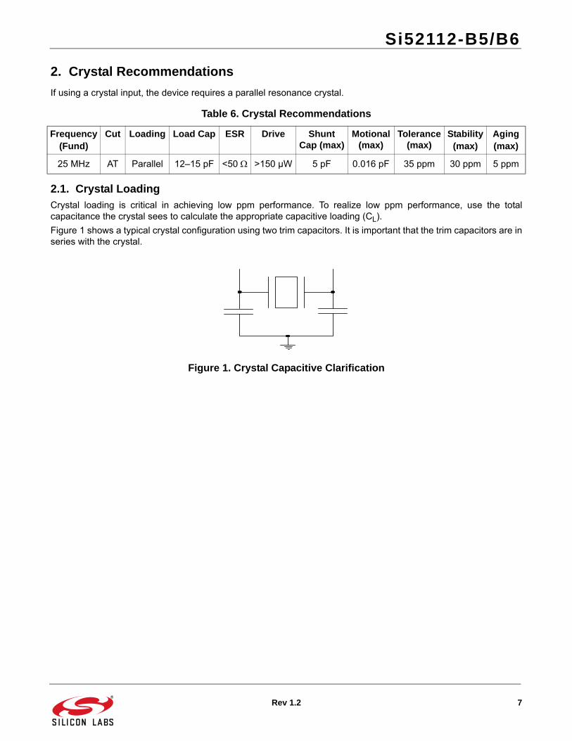
Figure 1 shows a typical crystal configuration using two trim capacitors. It is important that the trim capacitors are inseries with the crystal.
Figure 1. Crystal Capacitive Clarification
Table 6. Crystal Recommendations
Frequency(Fund)
Cut Loading Load Cap ESR Drive Shunt Cap (max)
Motional (max)
Tolerance (max)
Stability(max)
Aging(max)
25 MHz AT Parallel 12–15 pF <50 >150 µW 5 pF 0.016 pF 35 ppm 30 ppm 5 ppm
Si52112-B5/B6
8 Rev 1.2
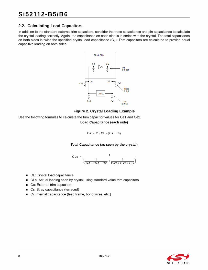
2.2. Calculating Load CapacitorsIn addition to the standard external trim capacitors, consider the trace capacitance and pin capacitance to calculatethe crystal loading correctly. Again, the capacitance on each side is in series with the crystal. The total capacitanceon both sides is twice the specified crystal load capacitance (CL). Trim capacitors are calculated to provide equalcapacitive loading on both sides.
Figure 2. Crystal Loading Example
Use the following formulas to calculate the trim capacitor values for Ce1 and Ce2.
Load Capacitance (each side)
Total Capacitance (as seen by the crystal)
CL: Crystal load capacitance
CLe: Actual loading seen by crystal using standard value trim capacitors
Ce: External trim capacitors
Cs: Stray capacitance (terraced)
Ci: Internal capacitance (lead frame, bond wires, etc.)
Ce 2 CL Cs Ci+ –=
CLe 1
1Ce1 Cs1 Ci1+ +--------------------------------------------- 1
Ce2 Cs2 Ci2+ +---------------------------------------------+
-------------------------------------------------------------------------------------------------------=
Si52112-B5/B6
Rev 1.2 9
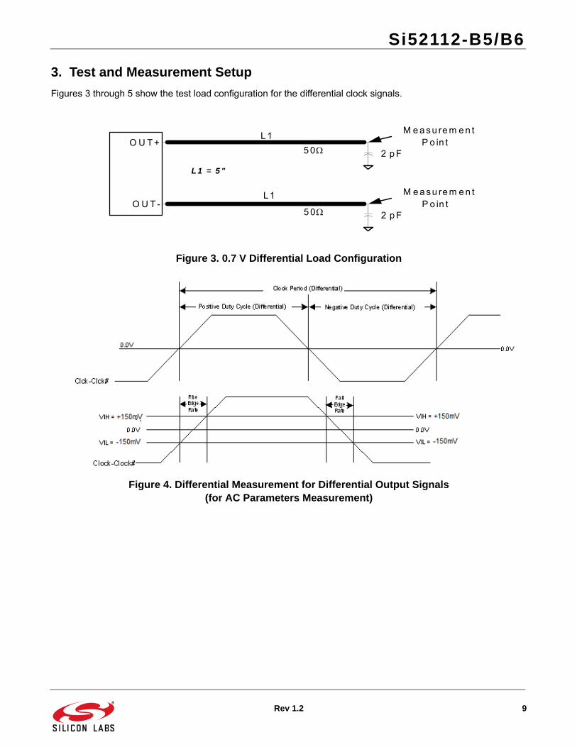
3. Test and Measurement Setup
Figures 3 through 5 show the test load configuration for the differential clock signals.
Figure 3. 0.7 V Differential Load Configuration
Figure 4. Differential Measurement for Differential Output Signals (for AC Parameters Measurement)
M e a s u re m e n tP o in t
2 p F5 0
M e a s u re m e n tP o in t
2 p F5 0
L 1
L 1 = 5 "
O U T +
O U T -L 1
Si52112-B5/B6
10 Rev 1.2
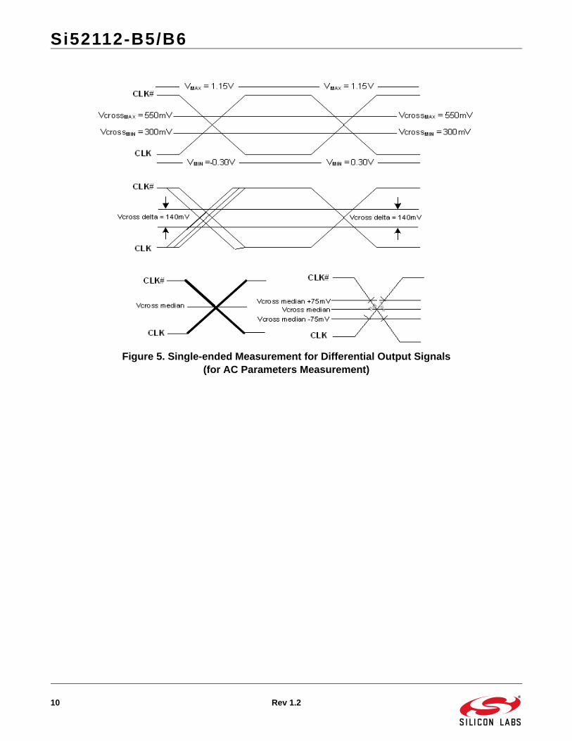
Figure 5. Single-ended Measurement for Differential Output Signals (for AC Parameters Measurement)
Si52112-B5/B6
Rev 1.2 11
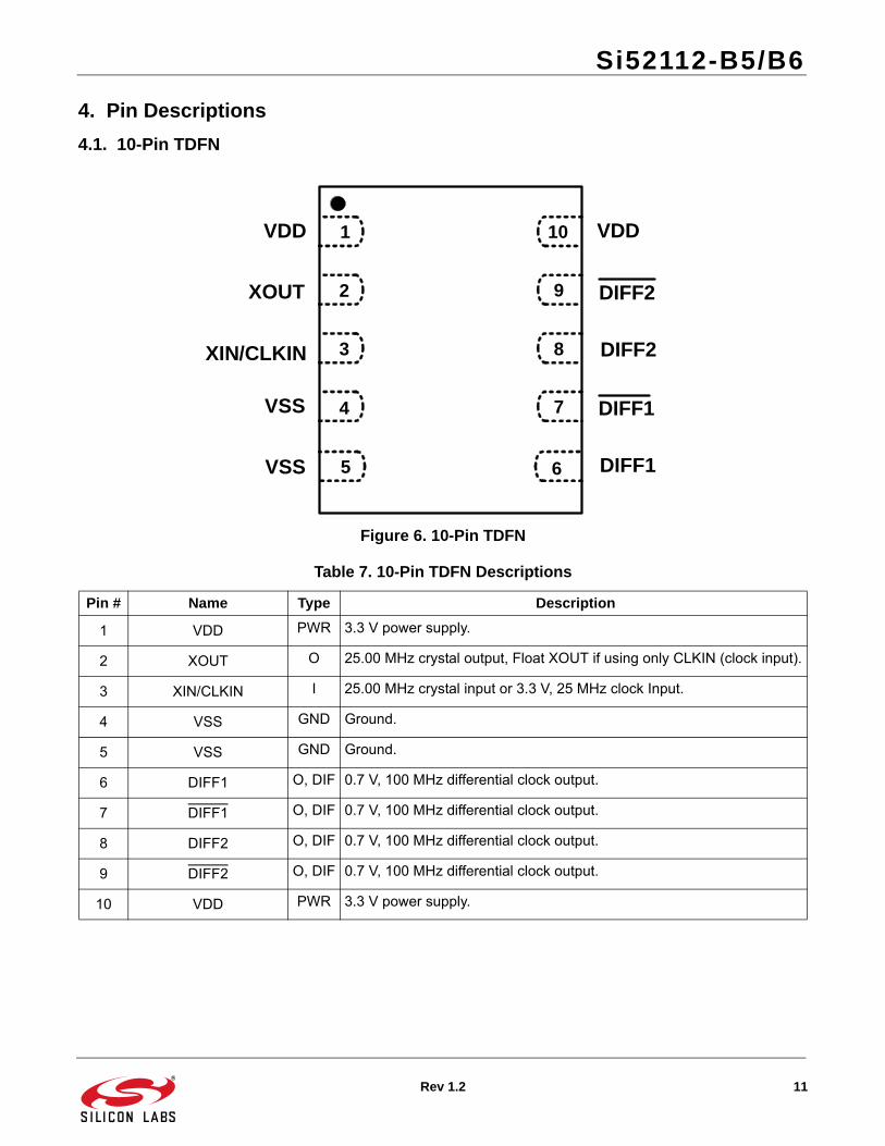
4. Pin Descriptions
4.1. 10-Pin TDFN
Figure 6. 10-Pin TDFN
Table 7. 10-Pin TDFN Descriptions
Pin # Name Type Description
1 VDD PWR 3.3 V power supply.
2 XOUT O 25.00 MHz crystal output, Float XOUT if using only CLKIN (clock input).
3 XIN/CLKIN I 25.00 MHz crystal input or 3.3 V, 25 MHz clock Input.
4 VSS GND Ground.
5 VSS GND Ground.
6 DIFF1 O, DIF 0.7 V, 100 MHz differential clock output.
7 DIFF1 O, DIF 0.7 V, 100 MHz differential clock output.
8 DIFF2 O, DIF 0.7 V, 100 MHz differential clock output.
9 DIFF2 O, DIF 0.7 V, 100 MHz differential clock output.
10 VDD PWR 3.3 V power supply.
10
9
8
7
1
2
3
4
VDDVDD
XOUT
XIN/CLKIN
VSS
VSS 5 6 DIFF1
DIFF1
DIFF2
DIFF2
Si52112-B5/B6
12 Rev 1.2
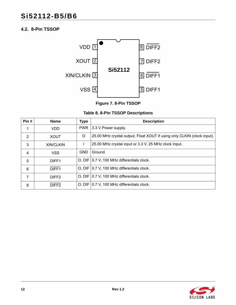
4.2. 8-Pin TSSOP
Figure 7. 8-Pin TSSOP
Table 8. 8-Pin TSSOP Descriptions
Pin # Name Type Description
1 VDD PWR 3.3 V Power supply.
2 XOUT O 25.00 MHz crystal output, Float XOUT if using only CLKIN (clock input).
3 XIN/CLKIN I 25.00 MHz crystal input or 3.3 V, 25 MHz clock Input.
4 VSS GND Ground.
5 DIFF1 O, DIF 0.7 V, 100 MHz differentials clock.
6 DIFF1 O, DIF 0.7 V, 100 MHz differentials clock.
7 DIFF2 O, DIF 0.7 V, 100 MHz differentials clock.
8 DIFF2 O, DIF 0.7 V, 100 MHz differentials clock.
8
Si52112
7
6
5 DIFF1
DIFF1
VDD
XOUT
XIN/CLKIN
VSS
1
2
3
4
DIFF2
DIFF2
Si52112-B5/B6
Rev 1.2 13
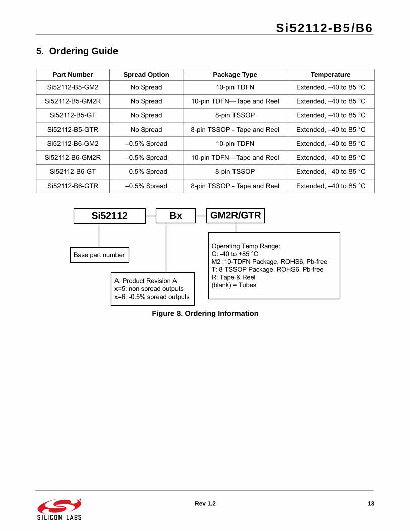
5. Ordering Guide
Figure 8. Ordering Information
Part Number Spread Option Package Type Temperature
Si52112-B5-GM2 No Spread 10-pin TDFN Extended, –40 to 85 °C
Si52112-B5-GM2R No Spread 10-pin TDFN—Tape and Reel Extended, –40 to 85 °C
Si52112-B5-GT No Spread 8-pin TSSOP Extended, –40 to 85 °C
Si52112-B5-GTR No Spread 8-pin TSSOP - Tape and Reel Extended, –40 to 85 °C
Si52112-B6-GM2 –0.5% Spread 10-pin TDFN Extended, –40 to 85 °C
Si52112-B6-GM2R –0.5% Spread 10-pin TDFN—Tape and Reel Extended, –40 to 85 °C
Si52112-B6-GT –0.5% Spread 8-pin TSSOP Extended, –40 to 85 °C
Si52112-B6-GTR –0.5% Spread 8-pin TSSOP - Tape and Reel Extended, –40 to 85 °C
Si52112 Bx GM2R/GTR
Base part number
A: Product Revision Ax=5: non spread outputsx=6: -0.5% spread outputs
Operating Temp Range: G: -40 to +85 °C M2 :10-TDFN Package, ROHS6, Pb-freeT: 8-TSSOP Package, ROHS6, Pb-freeR: Tape & Reel(blank) = Tubes
Si52112-B5/B6
14 Rev 1.2
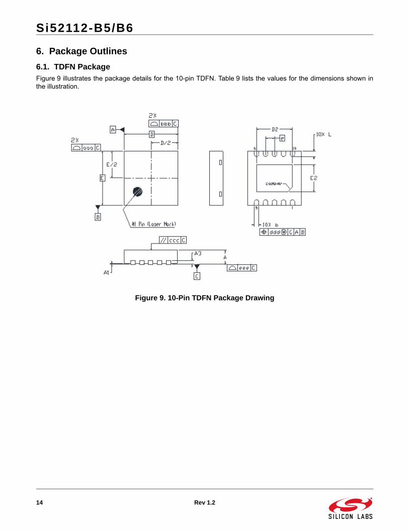
6. Package Outlines
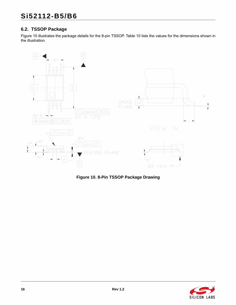
6.1. TDFN PackageFigure 9 illustrates the package details for the 10-pin TDFN. Table 9 lists the values for the dimensions shown inthe illustration.
Figure 9. 10-Pin TDFN Package Drawing
Si52112-B5/B6
Rev 1.2 15
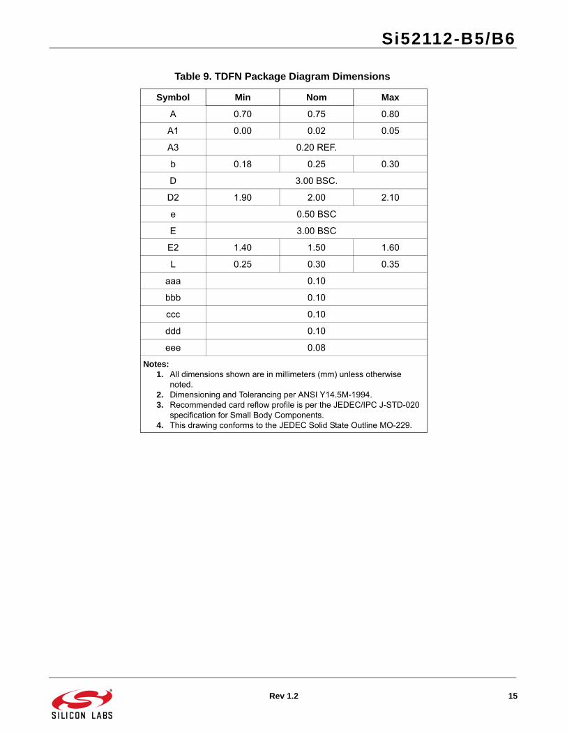
Table 9. TDFN Package Diagram Dimensions
Symbol Min Nom Max
A 0.70 0.75 0.80
A1 0.00 0.02 0.05
A3 0.20 REF.
b 0.18 0.25 0.30
D 3.00 BSC.
D2 1.90 2.00 2.10
e 0.50 BSC
E 3.00 BSC
E2 1.40 1.50 1.60
L 0.25 0.30 0.35
aaa 0.10
bbb 0.10
ccc 0.10
ddd 0.10
eee 0.08
Notes:1. All dimensions shown are in millimeters (mm) unless otherwise
noted.2. Dimensioning and Tolerancing per ANSI Y14.5M-1994.3. Recommended card reflow profile is per the JEDEC/IPC J-STD-020
specification for Small Body Components.4. This drawing conforms to the JEDEC Solid State Outline MO-229.
Si52112-B5/B6
16 Rev 1.2
6.2. TSSOP PackageFigure 10 illustrates the package details for the 8-pin TSSOP. Table 10 lists the values for the dimensions shown inthe illustration.
Figure 10. 8-Pin TSSOP Package Drawing
Si52112-B5/B6
Rev 1.2 17
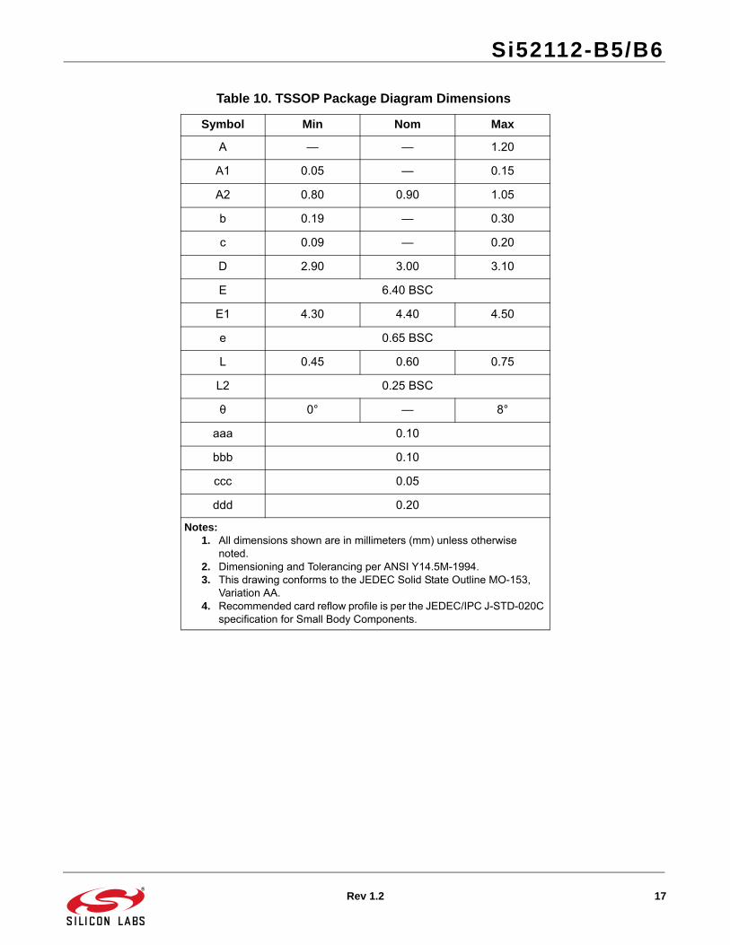
Table 10. TSSOP Package Diagram Dimensions
Symbol Min Nom Max
A — — 1.20
A1 0.05 — 0.15
A2 0.80 0.90 1.05
b 0.19 — 0.30
c 0.09 — 0.20
D 2.90 3.00 3.10
E 6.40 BSC
E1 4.30 4.40 4.50
e 0.65 BSC
L 0.45 0.60 0.75
L2 0.25 BSC
θ 0° — 8°
aaa 0.10
bbb 0.10
ccc 0.05
ddd 0.20
Notes:1. All dimensions shown are in millimeters (mm) unless otherwise
noted.2. Dimensioning and Tolerancing per ANSI Y14.5M-1994.3. This drawing conforms to the JEDEC Solid State Outline MO-153,
Variation AA.4. Recommended card reflow profile is per the JEDEC/IPC J-STD-020C
specification for Small Body Components.
Si52112-B5/B6
18 Rev 1.2
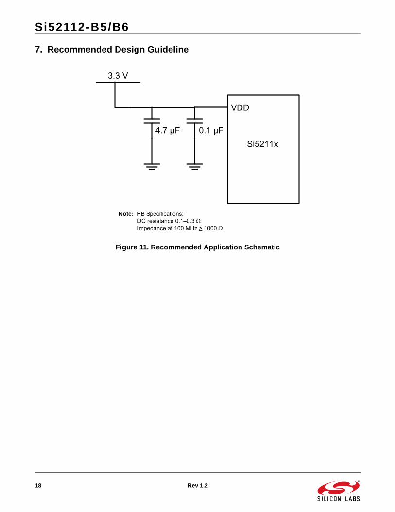
7. Recommended Design Guideline
Figure 11. Recommended Application Schematic
Note: FB Specifications:DC resistance 0.1–0.3 Impedance at 100 MHz > 1000
3.3 V
4.7 µF 0.1 µF
VDD
Si5211x
Si52112-B5/B6
Rev 1.2 19
DOCUMENT CHANGE LIST
Revision 1.0 to Revision 1.1 Added “4.2. 8-Pin TSSOP” pin description on
page 12.
Revision 1.1 to Revision 1.2 Updated Features on page 1.
Updated Description on page 1.
Updated Table 3, “AC Electrical Specifications,” on page 5.
DisclaimerSilicon Laboratories intends to provide customers with the latest, accurate, and in-depth documentation of all peripherals and modules available for system and software implementers using or intending to use the Silicon Laboratories products. Characterization data, available modules and peripherals, memory sizes and memory addresses refer to each specific device, and "Typical" parameters provided can and do vary in different applications. Application examples described herein are for illustrative purposes only. Silicon Laboratories reserves the right to make changes without further notice and limitation to product information, specifications, and descriptions herein, and does not give warranties as to the accuracy or completeness of the included information. Silicon Laboratories shall have no liability for the consequences of use of the information supplied herein. This document does not imply or express copyright licenses granted hereunder to design or fabricate any integrated circuits. The products must not be used within any Life Support System without the specific written consent of Silicon Laboratories. A "Life Support System" is any product or system intended to support or sustain life and/or health, which, if it fails, can be reasonably expected to result in significant personal injury or death. Silicon Laboratories products are generally not intended for military applications. Silicon Laboratories products shall under no circumstances be used in weapons of mass destruction including (but not limited to) nuclear, biological or chemical weapons, or missiles capable of delivering such weapons.
Trademark InformationSilicon Laboratories Inc., Silicon Laboratories, Silicon Labs, SiLabs and the Silicon Labs logo, CMEMS®, EFM, EFM32, EFR, Energy Micro, Energy Micro logo and combinations thereof, "the world’s most energy friendly microcontrollers", Ember®, EZLink®, EZMac®, EZRadio®, EZRadioPRO®, DSPLL®, ISOmodem ®, Precision32®, ProSLIC®, SiPHY®, USBXpress® and others are trademarks or registered trademarks of Silicon Laboratories Inc. ARM, CORTEX, Cortex-M3 and THUMB are trademarks or registered trademarks of ARM Holdings. Keil is a registered trademark of ARM Limited. All other products or brand names mentioned herein are trademarks of their respective holders.
http://www.silabs.com
Silicon Laboratories Inc.400 West Cesar ChavezAustin, TX 78701USA
ClockBuilder Pro
One-click access to Timing tools, documentation, software, source code libraries & more. Available for Windows and iOS (CBGo only).
www.silabs.com/CBPro
Timing Portfoliowww.silabs.com/timing
SW/HWwww.silabs.com/CBPro
Qualitywww.silabs.com/quality
Support and Communitycommunity.silabs.com