Embed Size (px)
Citation preview
Silicon-based on-chip electrically tunable sidewallBragg grating Fabry–Perot filterWEIFENG ZHANG, NASRIN EHTESHAMI, WEILIN LIU, AND JIANPING YAO*Microwave Photonic Research Laboratory, School of Electrical Engineering and Computer Science, University of Ottawa,800 King Edward Avenue, Ottawa, Ontario K1N 6N5, Canada*Corresponding author: [email protected]
Received 15 April 2015; accepted 10 June 2015; posted 12 June 2015 (Doc. ID 238156); published 29 June 2015
We report the design, fabrication, and testing of a silicon-based on-chip electrically tunable sidewall Bragg gratingFabry–Perot filter. Spectral measurement shows that thefilter has a narrow notch in reflection of approximately46 pm, a Q-factor of 33,500, and an extinction ratio of16.4 dB. DC measurement shows that the average centralwavelength shift rates with forward and reverse bias are−1.15 nm∕V and 4.2 pm∕V, respectively. Due to stronglight confinement in the Fabry–Perot cavity, the electro-optic frequency response shows that the filter has a 3-dBmodulation bandwidth of ∼5.6 GHz. The performance ofusing the filter to perform modulation of a 3.5 Gb∕s 27 − 1nonreturn-to-zero pseudorandom binary sequence isevaluated. © 2015 Optical Society of America
OCIS codes: (250.0250) Optoelectronics; (050.2770) Gratings;
(130.3120) Integrated optics devices.
http://dx.doi.org/10.1364/OL.40.003153
Owing to the unique feature of a narrow transmission windowwithin its stopband, a Bragg grating Fabry–Perot filter (BG-FPF) [1,2] has been considered a key photonic component thatcan find numerous applications such as narrowband filtering[3], optical sensing [4], and optical signal processing [5]. Inaddition, a BG-FPF with an ultra-narrow transmission windowcan also be used in a photonic subsystem for mode selection.For example, a BG-FPF can be incorporated in a laser cavity toensure narrow linewidth operation [6]. In a high-capacity op-tical communications system where dense wavelength divisionmultiplexing (DWDM) is employed, accurate channelization isneeded, which can be implemented using an array of BG-FPFswith precisely controlled wavelength spacing [7]. However,the optical properties of a BG-FPF are predetermined by itsdesign, which is fixed once the device is fabricated. In addition,due to fabrication imperfections, there are always discrepanciesin the optical properties of an actually fabricated BG-FPF.Therefore, the fixed optical properties and the unavoidablefabrication discrepancies may limit BG-FPFs for wide appli-cations. Furthermore, for an adaptive sensor system and a
reconfigurable optical communication network, a frequency-tunable transmission filter is always required [8]. A frequency-tunable BG-FPF is a candidate for such applications.
In this Letter, we propose for the first time to the best of ourknowledge, a silicon-based on-chip electrically tunable sidewallBragg grating Fabry–Perot filter (TBG-FPF). The TBG-FPFconsists of two sidewall Bragg gratings on a rib waveguide astwo reflectors, and a lateral PN junction formed in the wave-guide to achieve electrical tunability. The tunability is achievedby tuning a bias voltage applied to the PN junction basedon the plasma dispersion effect. The TBG-FPF is designed,fabricated, and tested. Spectral measurement shows that thelinewidth of the notch in the reflection band is approximately46 pm with a Q-factor of 33,500, and an extinction ratio is16.4 dB. DC performance of the TBG-FPF is also evaluated.The average central wavelength shift rates for a forward andreverse bias are −1.15 nm∕V and 4.2 pm∕V, respectively.Since the light-confining resonating structure of the Fabry–Perot (FP) cavity can enhance the effect of refractive indexchange, the TBG-FPF can be employed as an electro-opticmodulator. The electro-optic frequency response is measuredthat shows a 3-dB modulation bandwidth of ∼5.6 GHz. Theperformance of using the filter as an electro-optic modulator toperform high-speed modulation of a 3.5 Gb∕s 27 − 1 non-return-to-zero pseudorandom binary sequence is evaluated.
Figure 1(a) illustrates the perspective view of the proposedTBG-FPF. It is fabricated on a silicon-on-insulator (SOI) sub-strate with a bottom silica layer of 2 μm in thickness and atop silicon layer of 220 nm in thickness. The cladding layerof silica is removed in Fig. 1(a) to clearly illustrate the internalstructure of the device. The silicon rib waveguide with 500-nmin width, 220-nm in height, and 90-nm in slab thickness isemployed to ensure a single fundamental TE mode operation.The inset in Fig. 1(a) shows a simulated mode profile of thefundamental TE mode at 1550 nm. To achieve a higher tuningefficiency, an asymmetrical lateral PN junction is adopted toenable electrical tuning of the grating based on the plasmadispersion effect [9]. As shown in Fig. 1(b), the PN junctionis slightly shifted to the left from the center of the waveguide by50 nm, to increase the mode overlap with the p-type dopingregion, since the plasma dispersion effect is more sensitive to
Letter Vol. 40, No. 13 / July 1 2015 / Optics Letters 3153
0146-9592/15/133153-04$15/0$15.00 © 2015 Optical Society of America
the change of the free-hole concentration. Additional p++ and n++ implantations, 1 μm away from the rib to minimize absorp-tion losses, are utilized for ohmic contact formation. Figure 1(c)provides the top view of the grating structure on the rib and theFP cavity. The periodic sidewall corrugations with a depth of75 nm are introduced to the rib. The grating period Λ is310 nm with a duty cycle of 50%, corresponding to aBragg wavelength of 1550 nm. The total length of the gratingis 1240 μm. The FP cavity, with a length L of 24.025 μm, isallocated at the center of the grating. Figure 1(d) shows theschematic layout of the device. Three TE-mode grating cou-plers [10] are used to couple light between the chip and theinput and output fibers, and a compact Y-branch [11] is usedto collect the reflected light. To minimize the chip footprintand reduce the bending loss, a strip waveguide is used to guidethe light signal between the grating coupler and the filter. Sincethe filter is designed on a rib waveguide, a double-layer lineartaper waveguide with a length of 50 μm is used for the tran-sition between the strip and the rib waveguides. Two contactwindows are opened on the silica pads, with 2-μm-thick alu-minum layer deposited to make the contacts. The entire deviceis 1.58 mm in length and 0.130 mm in width, giving a smallfootprint of 0.205 mm2.
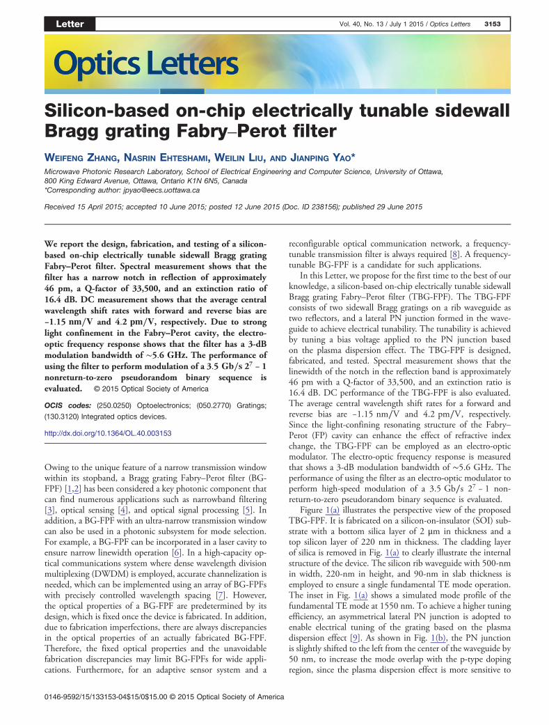
The optical performance of the TBG-FPF is first evaluated.To do so, we use an optical vector analyzer (LUNA OVA CTe)to measure the reflection and transmission spectra of the fab-ricated TBG-FPF. Figure 2 shows the spectra when a zero biasvoltage is applied. It can be seen there is a resonant windowwithin the stopband in the transmission spectrum. The notchin the reflection band has a 3-dB bandwidth of 46 pm with aQ-factor of 33,500, and an extinction ratio of 16.4 dB. The
Bragg wavelength is shifted to 1541.75 nm due to the inevi-table fabrication imperfections. Strong sidelobes in the reflec-tion spectrum are seen, which can be suppressed by applyingapodization to the grating [12]. The insertion loss of the TBG-FPF is 19 dB, which consists of the fiber-to-fiber I/O couplingloss of 15.6 dB, the grating induced loss of 2.1 dB, and the lossdue to the ion implantations of about 1.3 dB. Therefore, theoptical excess propagation loss caused by ion implantation is10.3 dB∕cm. Note that the fiber-to-fiber I/O coupling lossis measured using a reference rib waveguide without a gratingand without ion implantation. The grating induced loss, whichmainly results from the sidewall scattering, is measuredusing a reference sidewall grating on a rib waveguide withoution implantation.
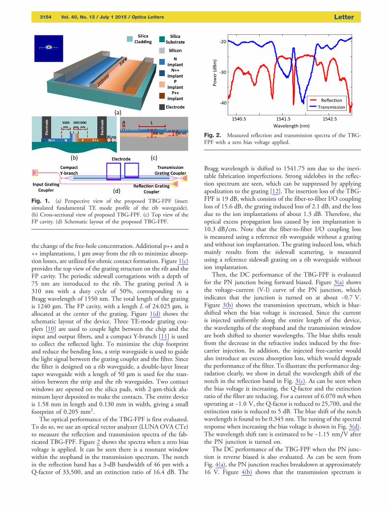
Then, the DC performance of the TBG-FPF is evaluatedfor the PN junction being forward biased. Figure 3(a) showsthe voltage–current (V-I) curve of the PN junction, whichindicates that the junction is turned on at about −0.7 V.Figure 3(b) shows the transmission spectrum, which is blue-shifted when the bias voltage is increased. Since the currentis injected uniformly along the entire length of the device,the wavelengths of the stopband and the transmission windoware both shifted to shorter wavelengths. The blue shifts resultfrom the decrease in the refractive index induced by the free-carrier injection. In addition, the injected free-carrier wouldalso introduce an excess absorption loss, which would degradethe performance of the filter. To illustrate the performance deg-radation clearly, we show in detail the wavelength shift of thenotch in the reflection band in Fig. 3(c). As can be seen whenthe bias voltage is increasing, the Q-factor and the extinctionratio of the filter are reducing. For a current of 6.070 mA whenoperating at −1.0 V, the Q-factor is reduced to 25,700, and theextinction ratio is reduced to 5 dB. The blue shift of the notchwavelength is found to be 0.345 nm. The tuning of the spectralresponse when increasing the bias voltage is shown in Fig. 3(d).The wavelength shift rate is estimated to be −1.15 nm∕V afterthe PN junction is turned on.
The DC performance of the TBG-FPF when the PN junc-tion is reverse biased is also evaluated. As can be seen fromFig. 4(a), the PN junction reaches breakdown at approximately16 V. Figure 4(b) shows that the transmission spectrum is
Fig. 1. (a) Perspective view of the proposed TBG-FPF (inset:simulated fundamental TE mode profile of the rib waveguide).(b) Cross-sectional view of proposed TBG-FPF. (c) Top view of theFP cavity. (d) Schematic layout of the proposed TBG-FPF.
Fig. 2. Measured reflection and transmission spectra of the TBG-FPF with a zero bias voltage applied.
3154 Vol. 40, No. 13 / July 1 2015 / Optics Letters Letter
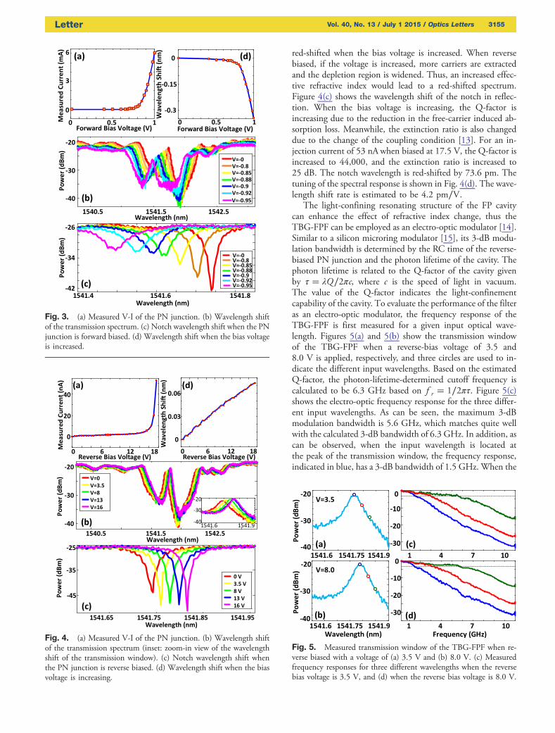
red-shifted when the bias voltage is increased. When reversebiased, if the voltage is increased, more carriers are extractedand the depletion region is widened. Thus, an increased effec-tive refractive index would lead to a red-shifted spectrum.Figure 4(c) shows the wavelength shift of the notch in reflec-tion. When the bias voltage is increasing, the Q-factor isincreasing due to the reduction in the free-carrier induced ab-sorption loss. Meanwhile, the extinction ratio is also changeddue to the change of the coupling condition [13]. For an in-jection current of 53 nA when biased at 17.5 V, the Q-factor isincreased to 44,000, and the extinction ratio is increased to25 dB. The notch wavelength is red-shifted by 73.6 pm. Thetuning of the spectral response is shown in Fig. 4(d). The wave-length shift rate is estimated to be 4.2 pm∕V.
The light-confining resonating structure of the FP cavitycan enhance the effect of refractive index change, thus theTBG-FPF can be employed as an electro-optic modulator [14].Similar to a silicon microring modulator [15], its 3-dB modu-lation bandwidth is determined by the RC time of the reverse-biased PN junction and the photon lifetime of the cavity. Thephoton lifetime is related to the Q-factor of the cavity givenby τ � λQ∕2πc, where c is the speed of light in vacuum.The value of the Q-factor indicates the light-confinementcapability of the cavity. To evaluate the performance of the filteras an electro-optic modulator, the frequency response of theTBG-FPF is first measured for a given input optical wave-length. Figures 5(a) and 5(b) show the transmission windowof the TBG-FPF when a reverse-bias voltage of 3.5 and8.0 V is applied, respectively, and three circles are used to in-dicate the different input wavelengths. Based on the estimatedQ-factor, the photon-lifetime-determined cutoff frequency iscalculated to be 6.3 GHz based on f r � 1∕2πτ. Figure 5(c)shows the electro-optic frequency response for the three differ-ent input wavelengths. As can be seen, the maximum 3-dBmodulation bandwidth is 5.6 GHz, which matches quite wellwith the calculated 3-dB bandwidth of 6.3 GHz. In addition, ascan be observed, when the input wavelength is located atthe peak of the transmission window, the frequency response,indicated in blue, has a 3-dB bandwidth of 1.5 GHz. When the
Fig. 3. (a) Measured V-I of the PN junction. (b) Wavelength shiftof the transmission spectrum. (c) Notch wavelength shift when the PNjunction is forward biased. (d) Wavelength shift when the bias voltageis increased.
Fig. 4. (a) Measured V-I of the PN junction. (b) Wavelength shiftof the transmission spectrum (inset: zoom-in view of the wavelengthshift of the transmission window). (c) Notch wavelength shift whenthe PN junction is reverse biased. (d) Wavelength shift when the biasvoltage is increasing.
Fig. 5. Measured transmission window of the TBG-FPF when re-verse biased with a voltage of (a) 3.5 V and (b) 8.0 V. (c) Measuredfrequency responses for three different wavelengths when the reversebias voltage is 3.5 V, and (d) when the reverse bias voltage is 8.0 V.
Letter Vol. 40, No. 13 / July 1 2015 / Optics Letters 3155
input wavelength is away from the peak of the transmissionwindow, the 3-dB bandwidth is increased to 3.1 GHz, as in-dicated in red in Fig. 5(c). When the input wavelength is far-ther away from the peak of the transmission window, the 3-dBbandwidth is further increased to 5.6 GHz, as indicated ingreen. As the wavelength of the input light is away from theresonance wavelength, the corresponding confinement capabil-ity of the cavity for that wavelength is becoming weaker, and itscorresponding photon lifetime is becoming shorter. Therefore,the measured 3-dB modulation bandwidth is becoming larger.This photon-lifetime-dependent frequency response confirmsthat the modulation bandwidth of this TBG-FPF is mainlylimited by the photon lifetime of the cavity. The same tendencyof the electro-optic frequency response is found in Fig. 5(d),which shows the frequency response when the PN junctionis reverse biased at 8.0 V.
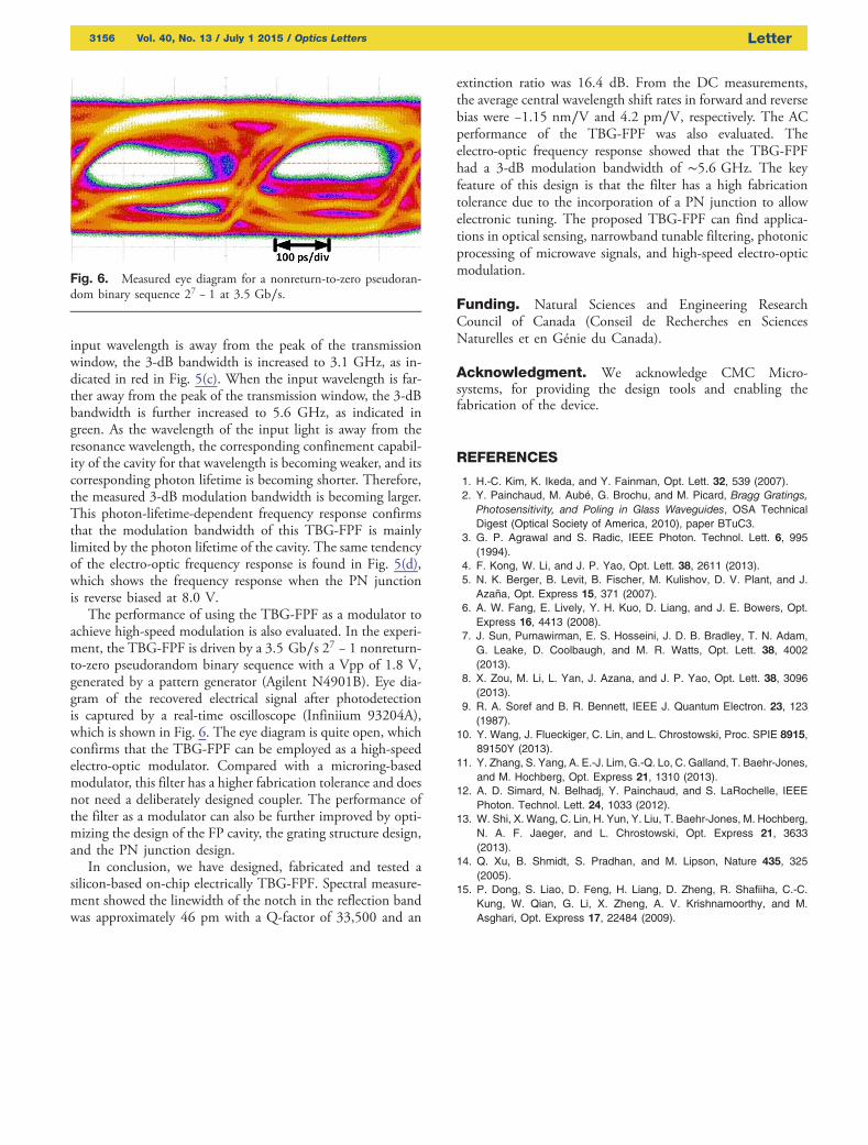
The performance of using the TBG-FPF as a modulator toachieve high-speed modulation is also evaluated. In the experi-ment, the TBG-FPF is driven by a 3.5 Gb∕s 27 − 1 nonreturn-to-zero pseudorandom binary sequence with a Vpp of 1.8 V,generated by a pattern generator (Agilent N4901B). Eye dia-gram of the recovered electrical signal after photodetectionis captured by a real-time oscilloscope (Infiniium 93204A),which is shown in Fig. 6. The eye diagram is quite open, whichconfirms that the TBG-FPF can be employed as a high-speedelectro-optic modulator. Compared with a microring-basedmodulator, this filter has a higher fabrication tolerance and doesnot need a deliberately designed coupler. The performance ofthe filter as a modulator can also be further improved by opti-mizing the design of the FP cavity, the grating structure design,and the PN junction design.
In conclusion, we have designed, fabricated and tested asilicon-based on-chip electrically TBG-FPF. Spectral measure-ment showed the linewidth of the notch in the reflection bandwas approximately 46 pm with a Q-factor of 33,500 and an
extinction ratio was 16.4 dB. From the DC measurements,the average central wavelength shift rates in forward and reversebias were −1.15 nm∕V and 4.2 pm∕V, respectively. The ACperformance of the TBG-FPF was also evaluated. Theelectro-optic frequency response showed that the TBG-FPFhad a 3-dB modulation bandwidth of ∼5.6 GHz. The keyfeature of this design is that the filter has a high fabricationtolerance due to the incorporation of a PN junction to allowelectronic tuning. The proposed TBG-FPF can find applica-tions in optical sensing, narrowband tunable filtering, photonicprocessing of microwave signals, and high-speed electro-opticmodulation.
Funding. Natural Sciences and Engineering ResearchCouncil of Canada (Conseil de Recherches en SciencesNaturelles et en Génie du Canada).
Acknowledgment. We acknowledge CMC Micro-systems, for providing the design tools and enabling thefabrication of the device.
REFERENCES
1. H.-C. Kim, K. Ikeda, and Y. Fainman, Opt. Lett. 32, 539 (2007).2. Y. Painchaud, M. Aubé, G. Brochu, and M. Picard, Bragg Gratings,
Photosensitivity, and Poling in Glass Waveguides, OSA TechnicalDigest (Optical Society of America, 2010), paper BTuC3.
3. G. P. Agrawal and S. Radic, IEEE Photon. Technol. Lett. 6, 995(1994).
4. F. Kong, W. Li, and J. P. Yao, Opt. Lett. 38, 2611 (2013).5. N. K. Berger, B. Levit, B. Fischer, M. Kulishov, D. V. Plant, and J.
Azaña, Opt. Express 15, 371 (2007).6. A. W. Fang, E. Lively, Y. H. Kuo, D. Liang, and J. E. Bowers, Opt.
Express 16, 4413 (2008).7. J. Sun, Purnawirman, E. S. Hosseini, J. D. B. Bradley, T. N. Adam,
G. Leake, D. Coolbaugh, and M. R. Watts, Opt. Lett. 38, 4002(2013).
8. X. Zou, M. Li, L. Yan, J. Azana, and J. P. Yao, Opt. Lett. 38, 3096(2013).
9. R. A. Soref and B. R. Bennett, IEEE J. Quantum Electron. 23, 123(1987).
10. Y. Wang, J. Flueckiger, C. Lin, and L. Chrostowski, Proc. SPIE 8915,89150Y (2013).
11. Y. Zhang, S. Yang, A. E.-J. Lim, G.-Q. Lo, C. Galland, T. Baehr-Jones,and M. Hochberg, Opt. Express 21, 1310 (2013).
12. A. D. Simard, N. Belhadj, Y. Painchaud, and S. LaRochelle, IEEEPhoton. Technol. Lett. 24, 1033 (2012).
13. W. Shi, X. Wang, C. Lin, H. Yun, Y. Liu, T. Baehr-Jones, M. Hochberg,N. A. F. Jaeger, and L. Chrostowski, Opt. Express 21, 3633(2013).
14. Q. Xu, B. Shmidt, S. Pradhan, and M. Lipson, Nature 435, 325(2005).
15. P. Dong, S. Liao, D. Feng, H. Liang, D. Zheng, R. Shafiiha, C.-C.Kung, W. Qian, G. Li, X. Zheng, A. V. Krishnamoorthy, and M.Asghari, Opt. Express 17, 22484 (2009).
Fig. 6. Measured eye diagram for a nonreturn-to-zero pseudoran-dom binary sequence 27 − 1 at 3.5 Gb∕s.
3156 Vol. 40, No. 13 / July 1 2015 / Optics Letters Letter