Embed Size (px)
Citation preview
Silicon-Carbide Power MOSFET Performance in High Efficiency Boost Power Processing Unit for Extreme Environments
Stanley A. Ikpe1, Jean-Marie Lauenstein2, Gregory A. Carr3, Don Hunter3, Lawrence L. Ludwig4 William Wood1, Linda Y. Del Castillo4 Fred Fitzpatrick1, Yuan Chen1
1NASA Langley Research Center Hampton, VA 23681 USA 2NASA Goddard Space Flight Center, Greenbelt, MD 20771 USA
3Jet Propulsion Laboratory, California Institute of Technology Pasadena, CA 91109 USA 4Kennedy Space Center, FL 32899 USA
Abstract - Silicon-Carbide (SiC) device technology has generated much interest in recent years. With superior thermal performance, power ratings and potential switching frequencies over its Silicon (Si) counterpart, SiC offers a greater possibility for high powered switching applications in extreme environment. In particular, SiC Metal-Oxide-Semiconductor Field-Effect Transistors’ (MOSFETs) maturing process technology has produced a plethora of commercially available power dense, low on-state resistance devices capable of switching at high frequencies. A novel hard-switched power processing unit (PPU) is implemented utilizing SiC power devices. Accelerated life data is captured and assessed in conjunction with a damage accumulation model of gate oxide and drain-source junction lifetime to evaluate potential system performance at high temperature environments.
Keywords - Silicon Carbide (SiC), MOSFETs, High Temperature Gate Bias, High Temperature Reverse Bias, Extreme Environment, Power Processing Unit
I. INTRODUCTION
Silicon-Carbide (SiC) device technology has generated much interest in recent years. With superior thermal performance, power rate, and switching frequencies over its Silicon (Si) counterpart, SiC offers a greater potential for high power switching applications in extreme environment. In particular, SiC Metal-Oxide-Semiconductor Field-Effect Transistors’ (MOSFETs) maturing process technology has produced a plethora of commercially available power dense, low on-state resistance devices capable of switching at high frequencies. The inherent material characteristics of SiC make it highly attractive for applications requiring a vast range of thermal robustness [1]. Though, successful switching applications have been demonstrated showcasing noteworthy performance metrics at high efficiency non-extraneous conditions [2-6]. This paper describes a design for reliability approach to implement a novel solar electric propulsion (SEP) system architecture which utilizes commercially available SiC Power MOSFETs in a multiphase hard-switching boost implementation. The work herein primarily focuses on the operation of the anode power supply subsystem of the proposed SiC High Temperature Boost (HTB) Power Processing Unit (PPU) [7]. This assembly employs a multi-phase straight boost topology to achieve high voltage DC/DC conversion. Commercial-off-the-shelf 1.2kV SiC Power
MOSFETs and Power Diodes from CREE Inc. are utilized to achieve the desired power conversion at high efficiency [8-10].
Figure 1 A schematic representation of a solar electric propulsion (SEP) architecture for in-space solar electric propulsion with integrated High Temperature Boost (HTB) Power Processing Unit (PPU). Photonic energy is converted to electricity by the solar array and the resultant energy is regulated and distributed by the Power Management and Distribution (PMAD) system providing an unregulated output power to the PPU. The anode power assembly module is composed of a typical straight boost design utilizing commercially available SiC MOSFETs and diodes for switching.
However, in order to achieve sustained long-term operation, it is imperative to fully understand the thermal and longstanding reliability limitations of such devices. Failure modes in SiC MOSFETs due to interstitial oxide traps and the SiO2/SiC interface states
https://ntrs.nasa.gov/search.jsp?R=20160009172 2020-03-28T00:20:16+00:00Z
have been well studied [11][12]. In characterizing these effects, we gain a more comprehensive understanding of the application-specific system reliability, as well as gauge the modules performance metrics at elevated temperatures. An efficiency model is then developed to characterize overall system efficiency due to deviations in dynamic MOSFET characteristics due to temperature.
In the design of switching power applications, it is critical to take into account the fluctuations in MOSFET characteristics such as on-state resistance due to prolonged operation and oxide degradation effects. SiC MOSFETs are highly susceptible to these modes of failure at high gate drive voltages. High Temperature Gate Bias (HTGB) and High Temperature Reverse Bias (HTRB) are common tests employed to assess device oxide and junction integrity respectively [13]. Using accelerated test data in conjunction with a damage accumulation model as described by the Arrhenius relationship, a nominal device lifetime with respect to the device junction temperature (TJ) can be extrapolated. Device lifetimes greater than 100 years are achievable under appropriate operational conditions.
II. EXERIMENTAL SETUP
First and second generation power MOSFET devices from CREE Inc. are considered in this work. Each device is encased in a standard TO-247-3 plastic package with voltage and current ratings of 1.2 kV and 20-90 A respectively. The MOSFET characteristics such as threshold voltage, breakdown voltage and on-state resistance are evaluated using High Temperature Gate Bias (HTGB) and High Temperature Reverse Bias (HTRB) characterization methods. Observing device performance at elevated temperatures helps accelerate common intrinsic failure modes within the devices, thus a nominal lifetime can be deduced from the response to each contributing failure mechanism. In particular, SiC MOSFET devices have been known to have high susceptibility to oxide failure modes at high temperatures due to band structure interactions at the oxide-semiconductor interface. Likewise, high drain-source voltage stress has also been known to contribute to oxide degradation. Therefore device evaluation at high temperatures proves critical to understand system performance in such environments.
A. High Temperature Gate Bias (HTGB)
HTGB characterization techniques are commonly employed to assess threshold voltage and on-state
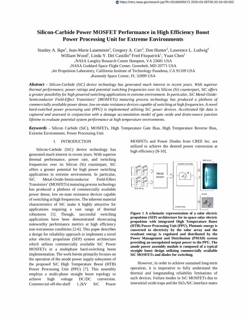
resistance shift do to thermal stress. An external DC voltage ranging from 20-40 V is continuously applied from gate-to-source (VGS) of the device under test (DUT) with a zero biased drain-source junction. The device junction temperature is maintained at constant temperature (typically much higher than the operational temperature range) in order to induce failure modes representative of devices under operational conditions. The device junction temperature is assumed to be approximately equal to the ambient temperature ranging from 125-150°C. Keithley Source Measurement Units (SMU) are configured to monitor the DUT voltage and current characteristics. A sample size of 3-5 devices per bias condition is considered. Figure 1 depicts the characterization setup.
Figure 2 A schematic of High Temperature Gate Bias characterization setup.
B. High Temperature Reverse Bias (HTRB)
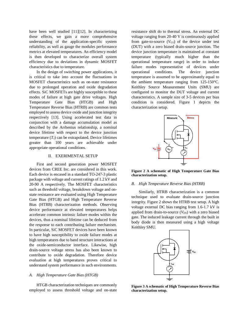
Similarly, HTRB characterization is a common technique used to evaluate drain-source junction integrity. Figure 2 shows the HTRB test setup. A high voltage external DC bias ranging from 1.6-1.7 kV is applied from drain-to-source (VDS) with a zero biased gate. The induced leakage current through the built in body diode is then measured using a high voltage Keithley SMU.
Figure 3 A schematic of High Temperature Reverse Bias characterization setup.
III. RESULTS AND DISCUSSION
A. SiC MOSFET Long-Term Reliability
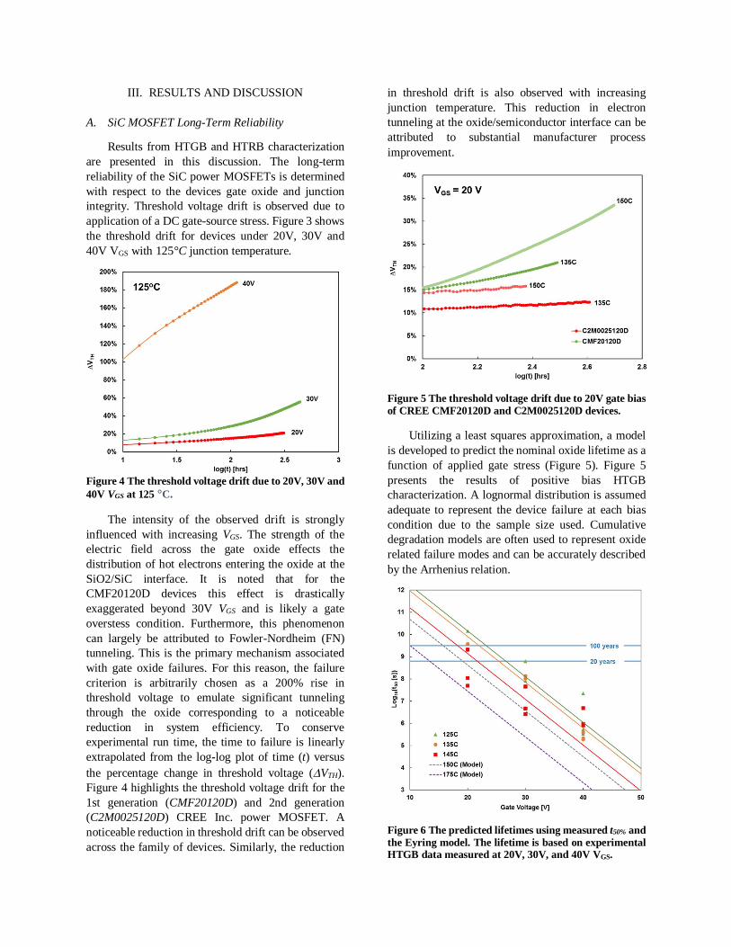
Results from HTGB and HTRB characterization are presented in this discussion. The long-term reliability of the SiC power MOSFETs is determined with respect to the devices gate oxide and junction integrity. Threshold voltage drift is observed due to application of a DC gate-source stress. Figure 3 shows the threshold drift for devices under 20V, 30V and 40V VGS with 125°C junction temperature.
Figure 4 The threshold voltage drift due to 20V, 30V and 40V VGS at 125 °C.
The intensity of the observed drift is strongly influenced with increasing VGS. The strength of the electric field across the gate oxide effects the distribution of hot electrons entering the oxide at the SiO2/SiC interface. It is noted that for the CMF20120D devices this effect is drastically exaggerated beyond 30V VGS and is likely a gate overstess condition. Furthermore, this phenomenon can largely be attributed to Fowler-Nordheim (FN) tunneling. This is the primary mechanism associated with gate oxide failures. For this reason, the failure criterion is arbitrarily chosen as a 200% rise in threshold voltage to emulate significant tunneling through the oxide corresponding to a noticeable reduction in system efficiency. To conserve experimental run time, the time to failure is linearly extrapolated from the log-log plot of time (t) versus the percentage change in threshold voltage (VTH). Figure 4 highlights the threshold voltage drift for the 1st generation (CMF20120D) and 2nd generation (C2M0025120D) CREE Inc. power MOSFET. A noticeable reduction in threshold drift can be observed across the family of devices. Similarly, the reduction
in threshold drift is also observed with increasing junction temperature. This reduction in electron tunneling at the oxide/semiconductor interface can be attributed to substantial manufacturer process improvement.
Figure 5 The threshold voltage drift due to 20V gate bias of CREE CMF20120D and C2M0025120D devices.
Utilizing a least squares approximation, a model is developed to predict the nominal oxide lifetime as a function of applied gate stress (Figure 5). Figure 5 presents the results of positive bias HTGB characterization. A lognormal distribution is assumed adequate to represent the device failure at each bias condition due to the sample size used. Cumulative degradation models are often used to represent oxide related failure modes and can be accurately described by the Arrhenius relation.
Figure 6 The predicted lifetimes using measured t50% and the Eyring model. The lifetime is based on experimental HTGB data measured at 20V, 30V, and 40V VGS.
Using the E-model in conjunction with the Arrhenius relation, a pessimistic estimation model can be developed to correlate nominal device lifetime with applied gate stress. The voltage acceleration factor remains impartial to the device junction temperature and therefore is assumed to hold true for the entire temperature range in consideration. This suggests that a nominal oxide lifetime can in fact be determined for devices under similar operational conditions.
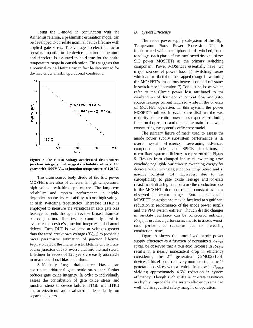
Figure 7 The HTRB voltage accelerated drain-source junction integrity test suggests reliability of over 120 years with 1000V VDS at junction temperature of 150 °C.
The drain-source body diode of the SiC power MOSFETs are also of concern in high temperature, high voltage switching applications. The long-term reliability and system performance is highly dependent on the device’s ability to block high voltage at high switching frequencies. Therefore HTRB is employed to measure the variations in zero gate bias leakage currents through a reverse biased drain-to-source junction. This test is commonly used to evaluate the device’s junction integrity and channel defects. Each DUT is evaluated at voltages greater than the rated breakdown voltage (BVDSS) to provide a more pessimistic estimation of junction lifetime. Figure 6 depicts the characteristic lifetime of the drain-source junction due to reverse bias and thermal stress. Lifetimes in excess of 120 years are easily attainable in near operational bias conditions.
Sufficiently large drain-source biases can contribute additional gate oxide stress and further reduces gate oxide integrity. In order to individually assess the contribution of gate oxide stress and junction stress to device failure, HTGB and HTRB characterizations are evaluated independently on separate devices.
B. System Efficiency
The anode power supply subsystem of the High Temperature Boost Power Processing Unit is implemented with a multiphase hard-switched, boost topology. Each phase of the interleaved design utilizes SiC power MOSFETs as the primary switching component. Power MOSFETs essentially have two major sources of power loss: 1) Switching losses which are attributed to the trapped charge flow during the MOSFET’s transitions between on and off states in switch-mode operation. 2) Conduction losses which refer to the Ohmic power loss attributed to the combination of drain-source current flow and gate-source leakage current incurred while in the on-state of MOSFET operation. In this system, the power MOSFETs utilized in each phase dissipate the vast majority of the entire power loss experienced during functional operation and thus is the main focus when constructing the system’s efficiency model.
The primary figure of merit used to assess the anode power supply subsystem performance is its overall system efficiency. Leveraging advanced component models and SPICE simulations, a normalized system efficiency is represented in Figure 9. Results from clamped inductive switching tests conclude negligible variation in switching energy for devices with increasing junction temperature and is assume constant [14]. However, due to the susceptibility to gate oxide leakage and on-state resistance drift at high temperature the conduction loss in the MOSFETs does not remain constant over the observed temperature range. Extreme changes in MOSFET on-resistance may in fact lead to significant reduction in performance of the anode power supply and the PPU system entirely. Though drastic changes in on-state resistance can be considered unlikely, RDS(on) is used as a performance metric to assess worst-case performance scenarios due to increasing conduction losses.
Figure 9 shows the normalized anode power supply efficiency as a function of normalized RDS(on). It can be observed that a four-fold increase in RDS(on)
results in a nearly nonexistent drop in efficiency considering the 2nd generation C2M0025120D devices. This effect is relatively more drastic in the 1st generation devices with a tenfold increase in RDS(on)
yielding approximately 4.6% reduction in system efficiency. Though such shifts in on-state resistance are highly improbable, the system efficiency remained well within specified safety margins of operation.
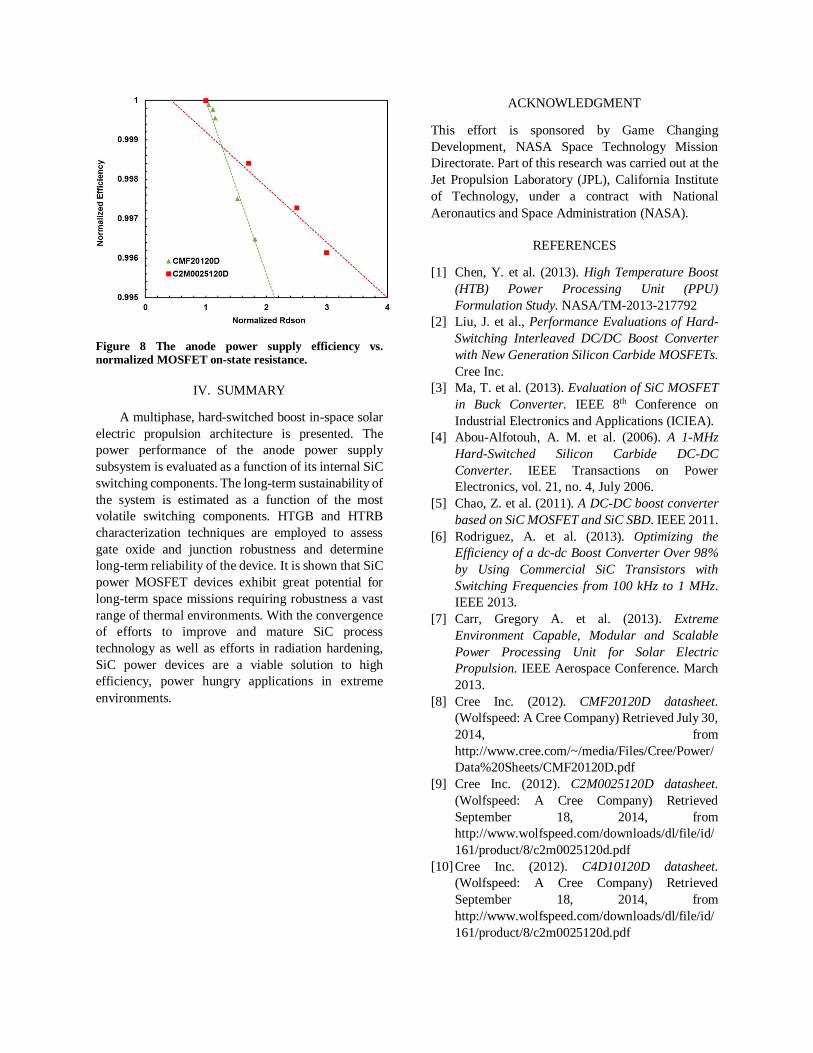
Figure 8 The anode power supply efficiency vs. normalized MOSFET on-state resistance.
IV. SUMMARY
A multiphase, hard-switched boost in-space solar electric propulsion architecture is presented. The power performance of the anode power supply subsystem is evaluated as a function of its internal SiC switching components. The long-term sustainability of the system is estimated as a function of the most volatile switching components. HTGB and HTRB characterization techniques are employed to assess gate oxide and junction robustness and determine long-term reliability of the device. It is shown that SiC power MOSFET devices exhibit great potential for long-term space missions requiring robustness a vast range of thermal environments. With the convergence of efforts to improve and mature SiC process technology as well as efforts in radiation hardening, SiC power devices are a viable solution to high efficiency, power hungry applications in extreme environments.
ACKNOWLEDGMENT
This effort is sponsored by Game Changing Development, NASA Space Technology Mission Directorate. Part of this research was carried out at the Jet Propulsion Laboratory (JPL), California Institute of Technology, under a contract with National Aeronautics and Space Administration (NASA).
REFERENCES
[1] Chen, Y. et al. (2013). High Temperature Boost (HTB) Power Processing Unit (PPU) Formulation Study. NASA/TM-2013-217792
[2] Liu, J. et al., Performance Evaluations of Hard-Switching Interleaved DC/DC Boost Converter with New Generation Silicon Carbide MOSFETs. Cree Inc.
[3] Ma, T. et al. (2013). Evaluation of SiC MOSFET in Buck Converter. IEEE 8th Conference on Industrial Electronics and Applications (ICIEA).
[4] Abou-Alfotouh, A. M. et al. (2006). A 1-MHz Hard-Switched Silicon Carbide DC-DC Converter. IEEE Transactions on Power Electronics, vol. 21, no. 4, July 2006.
[5] Chao, Z. et al. (2011). A DC-DC boost converter based on SiC MOSFET and SiC SBD. IEEE 2011.
[6] Rodriguez, A. et al. (2013). Optimizing the Efficiency of a dc-dc Boost Converter Over 98% by Using Commercial SiC Transistors with Switching Frequencies from 100 kHz to 1 MHz. IEEE 2013.
[7] Carr, Gregory A. et al. (2013). Extreme Environment Capable, Modular and Scalable Power Processing Unit for Solar Electric Propulsion. IEEE Aerospace Conference. March 2013.
[8] Cree Inc. (2012). CMF20120D datasheet. (Wolfspeed: A Cree Company) Retrieved July 30, 2014, from http://www.cree.com/~/media/Files/Cree/Power/Data%20Sheets/CMF20120D.pdf
[9] Cree Inc. (2012). C2M0025120D datasheet. (Wolfspeed: A Cree Company) Retrieved September 18, 2014, from http://www.wolfspeed.com/downloads/dl/file/id/161/product/8/c2m0025120d.pdf
[10] Cree Inc. (2012). C4D10120D datasheet. (Wolfspeed: A Cree Company) Retrieved September 18, 2014, from http://www.wolfspeed.com/downloads/dl/file/id/161/product/8/c2m0025120d.pdf
[11] Yu, L. C. et al. (2010). Reliability Issues of SiC MOSFETs: A Technology for High-Temperature Environments. IEEE Transactions on Device and Materials Reliability, Vol., 10, No. 4, Dec. 2010
[12] Treu, M. et al. (2010). Reliability of SiC Power Devices and its Influence on their Commercialization – Review, Status, and Remaining Issues. IEEE IRPS, 2010.
[13] Yang, L. & Castellazzi, A. (2013). High temperature gate-bias and reverse-bias tests on SiC MOSFETs. Microelectronics Reliability, 53 pp. 1771-1773.
[14] Ikpe, S. et al (2016). Long-Term Reliability of a Hard-Switched Boost Power Processing Unit Utilizing SiC Power MOSFETs. IEEE International Reliability Physics Symposium. April 2016.