Embed Size (px)
Citation preview
&
www.cea.fr
Didier Belot; Alexandre Giry; Alexandre Siligaris; Baudouin Martineau; Ayssar Serhan; Pierre Ferris CEA‐LETI
« Silicon Power Amplifiers for 5G+ and IoT wireless communication applications”
Cliquez pour modifier le style du titre
DACLE Division| January 2014© CEA. All rights reserved | 2&
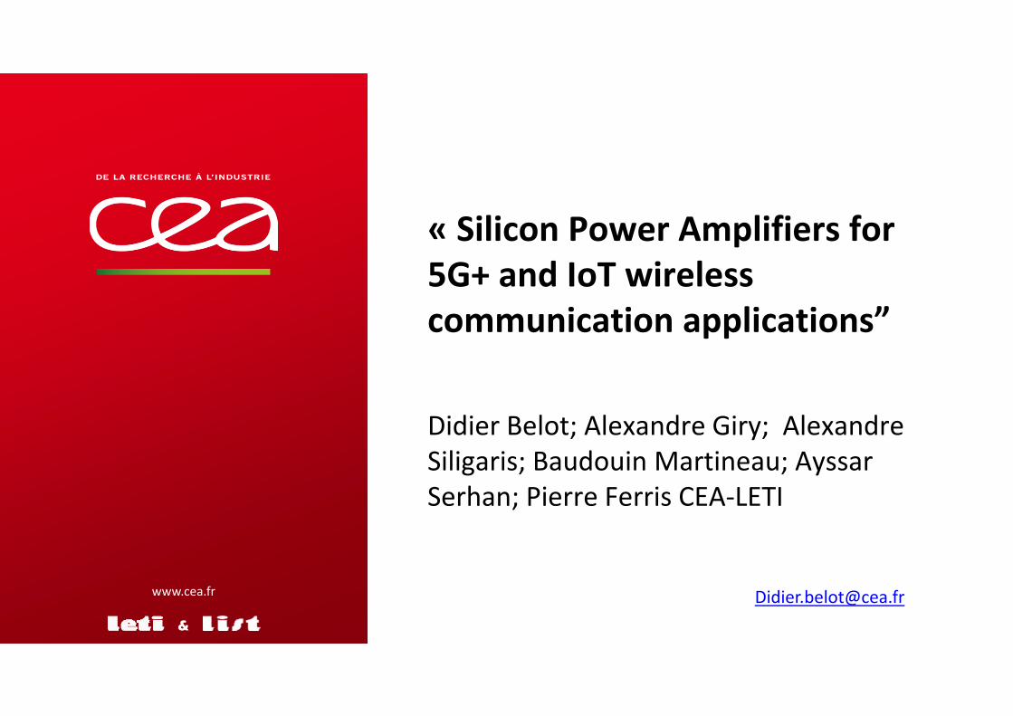
RF & WIRELESS 5G+ APPLICATIONS
Connectivity is everywhere; PA is in each Connectivity
Cliquez pour modifier le style du titre
DACLE Division| January 2014© CEA. All rights reserved | 3&
Outline
Introduction
Silicon Processes for Power Amplifiers
5G+ Applications & Design examples
Conclusions
Cliquez pour modifier le style du titre
DACLE Division| January 2014© CEA. All rights reserved | 4&
Introduction
Silicon Technology Evolution
Wireless Trends
Cliquez pour modifier le style du titre
DACLE Division| January 2014© CEA. All rights reserved | 5&
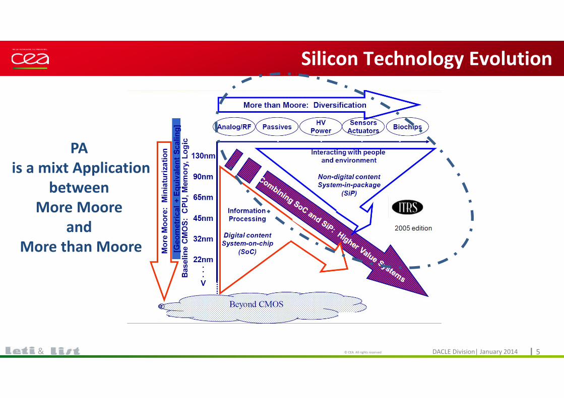
Silicon Technology Evolution
PA is a mixt Application
between More Moore
and More than Moore
Cliquez pour modifier le style du titre
DACLE Division| January 2014© CEA. All rights reserved | 6&
Wireless Trends
Reconfigurability:Data‐Rate, size, power consumption…Data/Range Efficiency
Low Cost and Modularity:Light Infrastructure
Safety and Security:Smart Interactive NetworkSense and React concept Secure links
Cliquez pour modifier le style du titre
DACLE Division| January 2014© CEA. All rights reserved | 7&
Silicon Processes for Power Amplifiers
CMOS Processes
SiGe HBT BiCMOS Processes
Summary
Cliquez pour modifier le style du titre
DACLE Division| January 2014© CEA. All rights reserved | 8&
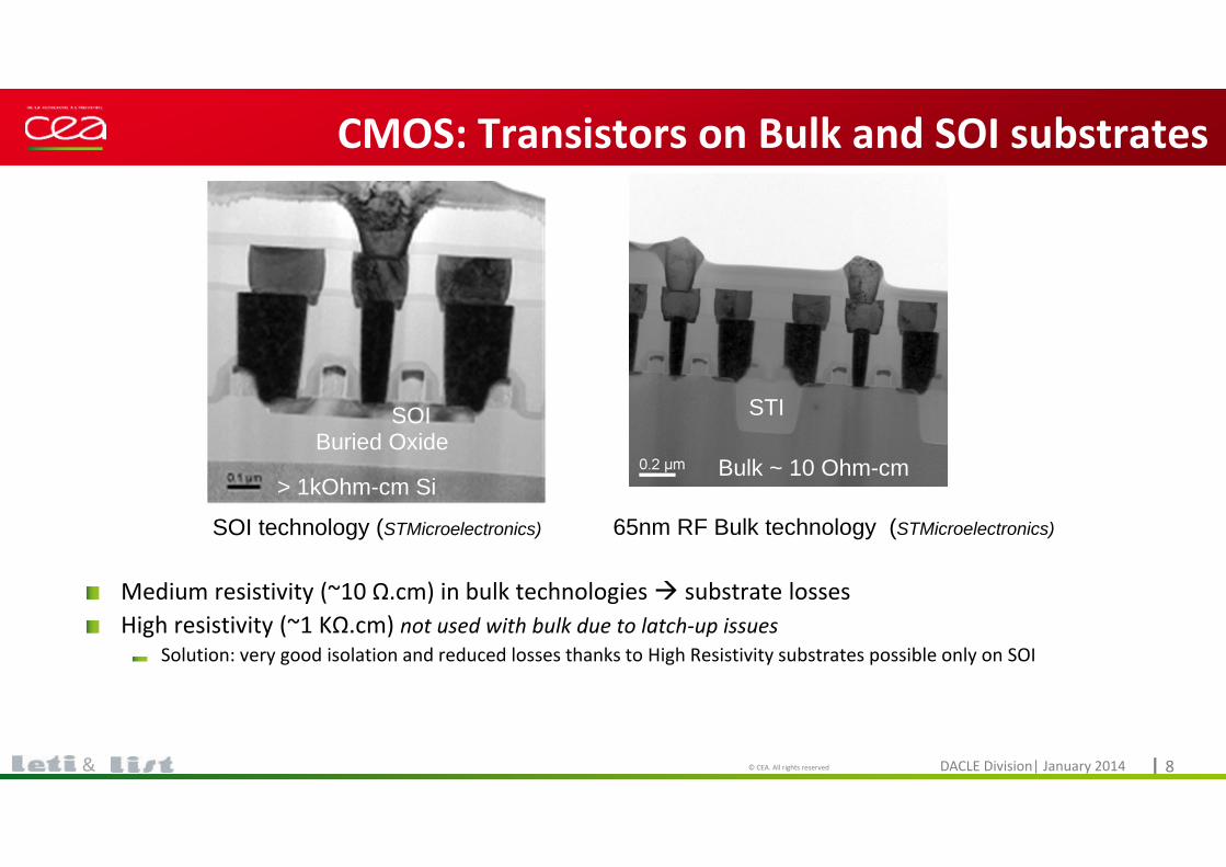
CMOS: Transistors on Bulk and SOI substrates
Medium resistivity (~10 Ω.cm) in bulk technologies substrate losses High resistivity (~1 KΩ.cm) not used with bulk due to latch‐up issues
Solution: very good isolation and reduced losses thanks to High Resistivity substrates possible only on SOI
Buried OxideSOI
> 1kOhm-cm Si
SOI technology (STMicroelectronics)
STI
Bulk ~ 10 Ohm-cm
65nm RF Bulk technology (STMicroelectronics)
Cliquez pour modifier le style du titre
DACLE Division| January 2014© CEA. All rights reserved | 9&
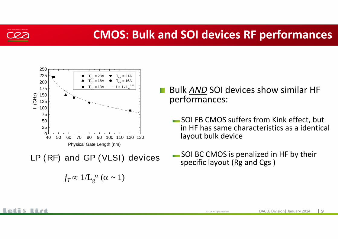
CMOS: Bulk and SOI devices RF performances
Bulk AND SOI devices show similar HF performances:
SOI FB CMOS suffers from Kink effect, but in HF has same characteristics as a identical layout bulk device
SOI BC CMOS is penalized in HF by their specific layout (Rg and Cgs )
40 50 60 70 80 90 100 110 120 1300
255075
100125150175200225250
TOX = 23A TOX = 21A TOX = 18A TOX = 16A
TOX = 13A f 1 / LG0.86
f T (G
Hz)
Physical Gate Length (nm)
LP (RF) and GP (VLSI) devices
fT 1/Lg ( ~ 1)
Cliquez pour modifier le style du titre
DACLE Division| January 2014© CEA. All rights reserved | 10& Giry Alexandre | March 2017
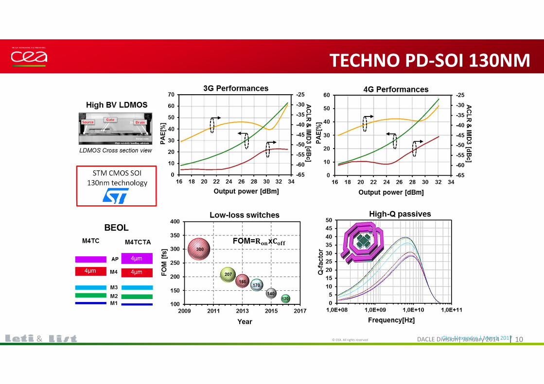
TECHNO PD‐SOI 130NM
STM CMOS SOI 130nm technology
Cliquez pour modifier le style du titre
DACLE Division| January 2014© CEA. All rights reserved | 11&
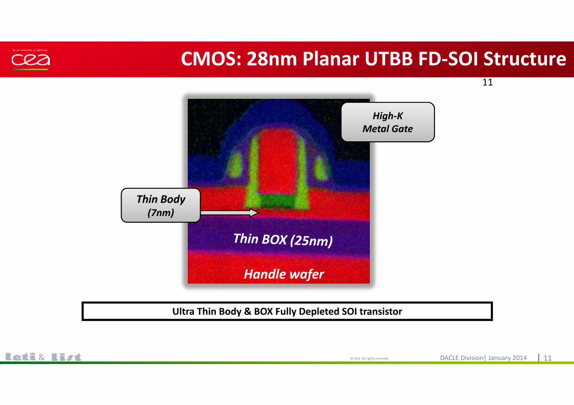
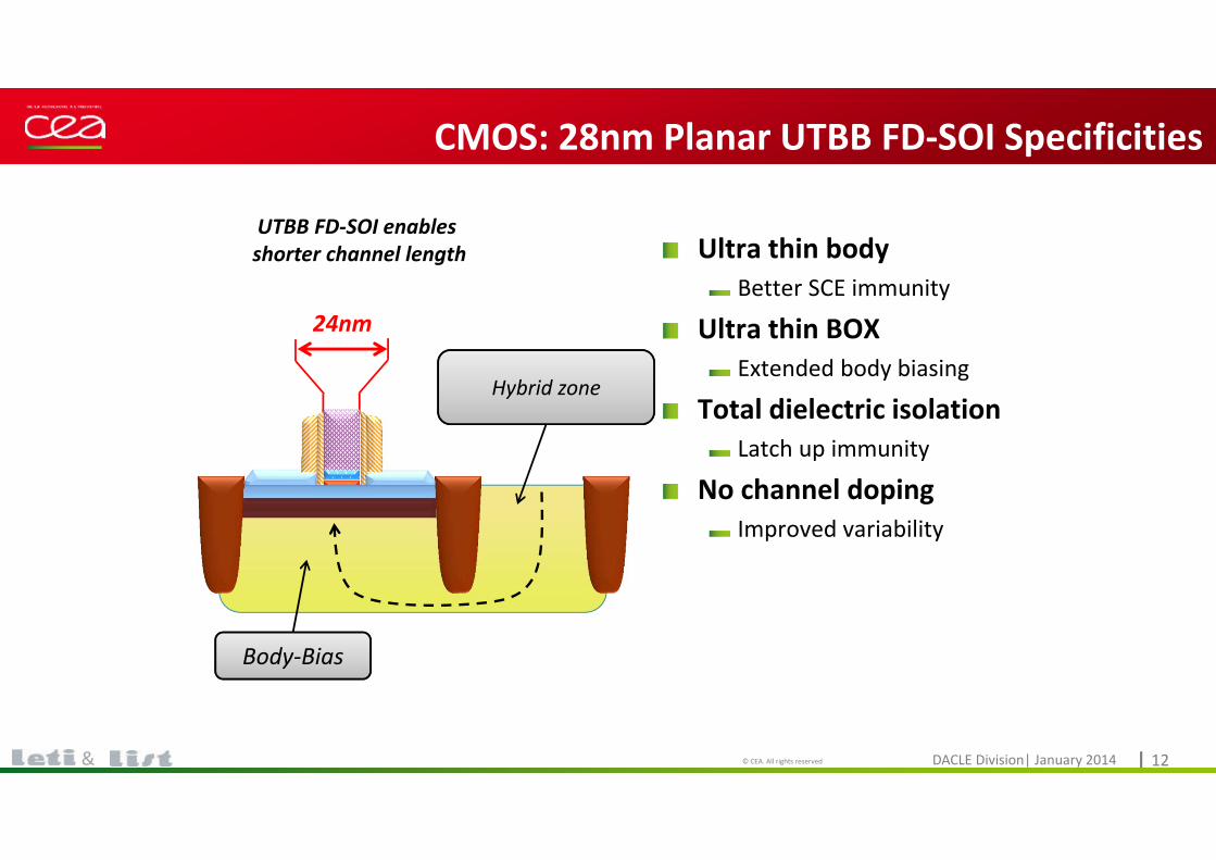
CMOS: 28nm Planar UTBB FD‐SOI Structure
Handle wafer
High‐KMetal Gate
Ultra Thin Body & BOX Fully Depleted SOI transistor
Thin Body(7nm)
11
Cliquez pour modifier le style du titre
DACLE Division| January 2014© CEA. All rights reserved | 12&
CMOS: 28nm Planar UTBB FD‐SOI Specificities
Body‐Bias
Hybrid zone
24nm
Ultra thin bodyBetter SCE immunity
Ultra thin BOXExtended body biasing
Total dielectric isolationLatch up immunity
No channel dopingImproved variability
UTBB FD‐SOI enables shorter channel length
Cliquez pour modifier le style du titre
DACLE Division| January 2014© CEA. All rights reserved | 13&
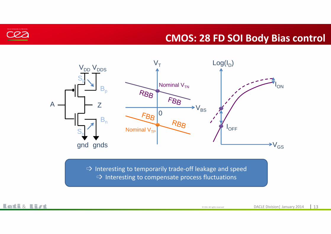
CMOS: 28 FD SOI Body Bias control
Nominal VTN
Nominal VTP
0VBS
VT
gnd gnds
A Z
Bn
Sn
Bp
Sp
VDD VDDS
VGS
Log(ID)
IOFF
ION
➩ Interesting to temporarily trade‐off leakage and speed➩ Interesting to compensate process fluctuations
13
Cliquez pour modifier le style du titre
DACLE Division| January 2014© CEA. All rights reserved | 14&
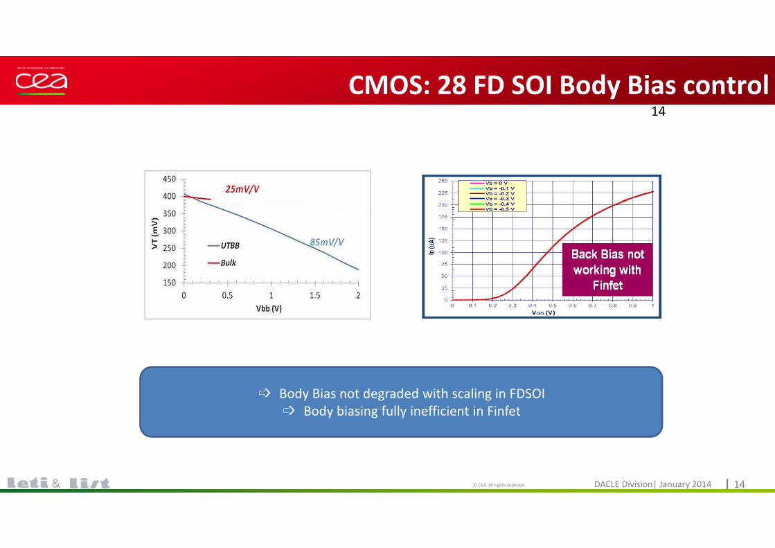
CMOS: 28 FD SOI Body Bias control
➩ Body Bias not degraded with scaling in FDSOI➩ Body biasing fully inefficient in Finfet
14
Cliquez pour modifier le style du titre
DACLE Division| January 2014© CEA. All rights reserved | 15&
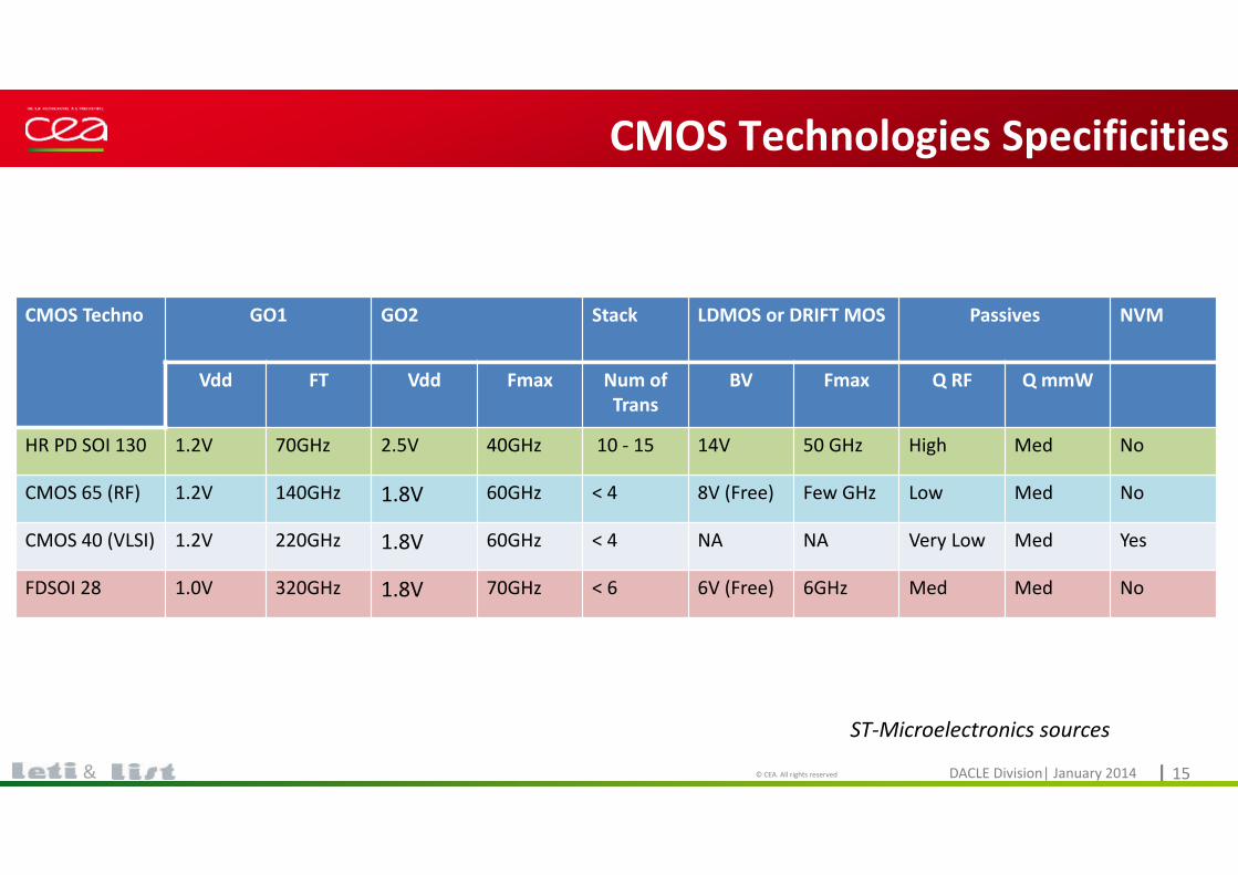
CMOS Technologies Specificities
CMOS Techno GO1 GO2 Stack LDMOS or DRIFT MOS Passives NVM
Vdd FT Vdd Fmax Num of Trans
BV Fmax Q RF Q mmW
HR PD SOI 130 1.2V 70GHz 2.5V 40GHz 10 ‐ 15 14V 50 GHz High Med No
CMOS 65 (RF) 1.2V 140GHz 1.8V 60GHz < 4 8V (Free) Few GHz Low Med No
CMOS 40 (VLSI) 1.2V 220GHz 1.8V 60GHz < 4 NA NA Very Low Med Yes
FDSOI 28 1.0V 320GHz 1.8V 70GHz < 6 6V (Free) 6GHz Med Med No
ST‐Microelectronics sources
Cliquez pour modifier le style du titre
DACLE Division| January 2014© CEA. All rights reserved | 16&
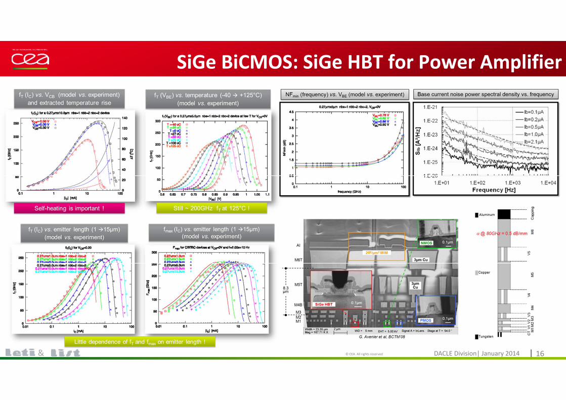
SiGe BiCMOS: SiGe HBT for Power Amplifier
Cliquez pour modifier le style du titre
DACLE Division| January 2014© CEA. All rights reserved | 17&
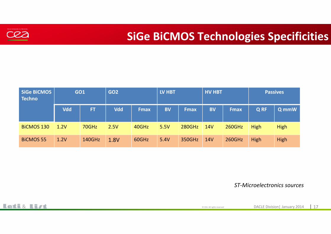
SiGe BiCMOS Technologies Specificities
SiGe BiCMOSTechno
GO1 GO2 LV HBT HV HBT Passives
Vdd FT Vdd Fmax BV Fmax BV Fmax Q RF Q mmW
BiCMOS 130 1.2V 70GHz 2.5V 40GHz 5.5V 280GHz 14V 260GHz High High
BiCMOS 55 1.2V 140GHz 1.8V 60GHz 5.4V 350GHz 14V 260GHz High High
ST‐Microelectronics sources
Cliquez pour modifier le style du titre
DACLE Division| January 2014© CEA. All rights reserved | 18&
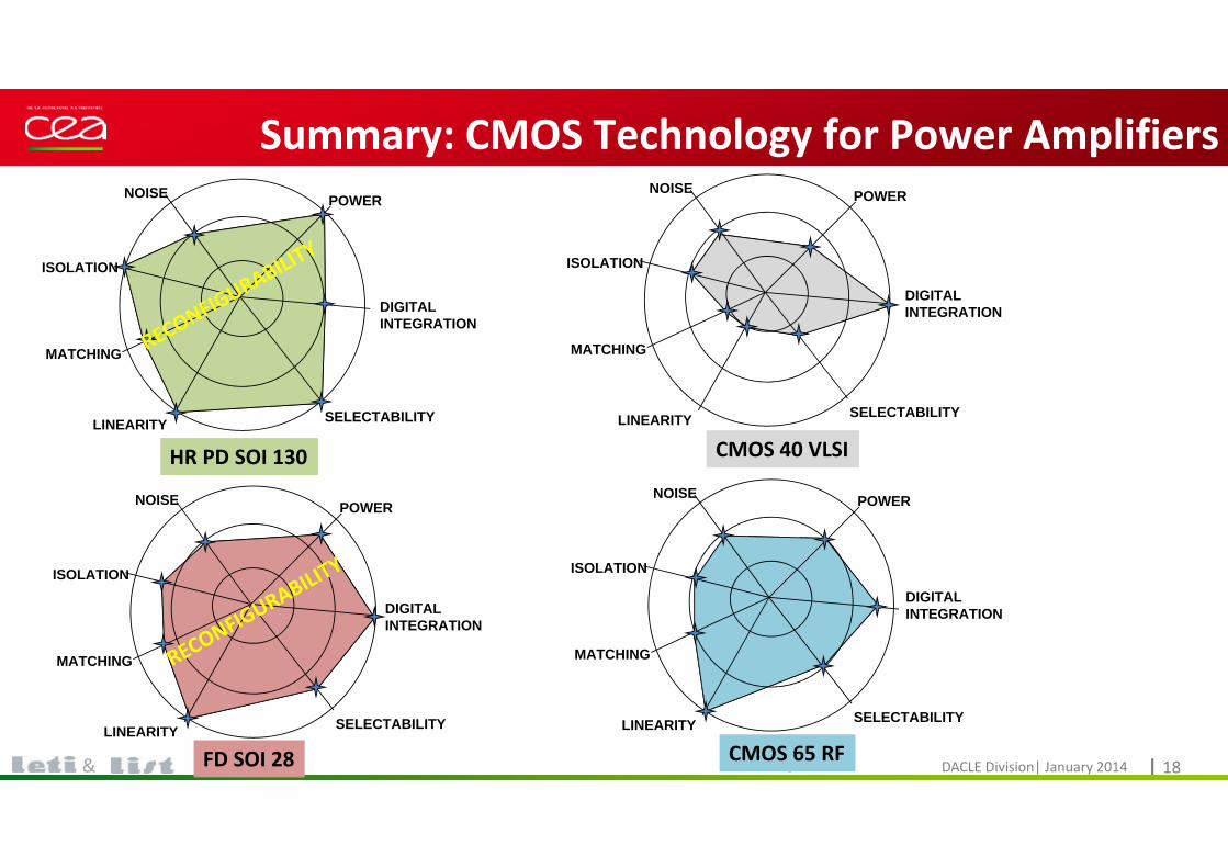
Summary: CMOS Technology for Power Amplifiers
HR PD SOI 130
NOISE
ISOLATION
SELECTABILITY
POWER
LINEARITY
MATCHING
CMOS 40 VLSI
NOISE
ISOLATION
SELECTABILITY
POWER
LINEARITY
MATCHING
CMOS 65 RFFD SOI 28
NOISE
ISOLATION
SELECTABILITY
POWER
LINEARITY
MATCHING
NOISE
ISOLATION
SELECTABILITY
DIGITALINTEGRATION
POWER
LINEARITY
MATCHING
DIGITALINTEGRATION
DIGITALINTEGRATIONDIGITAL
INTEGRATION
Cliquez pour modifier le style du titre
DACLE Division| January 2014© CEA. All rights reserved | 19&
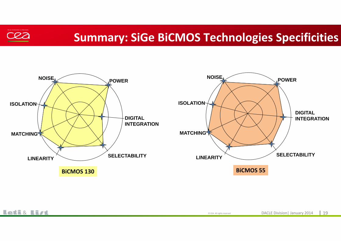
Summary: SiGe BiCMOS Technologies Specificities
NOISE
ISOLATION
SELECTABILITY
POWER
LINEARITY
MATCHING
BiCMOS 130 BiCMOS 55
NOISE
ISOLATION
SELECTABILITY
POWER
LINEARITY
MATCHING
DIGITALINTEGRATION
DIGITALINTEGRATION
Cliquez pour modifier le style du titre
DACLE Division| January 2014© CEA. All rights reserved | 20&
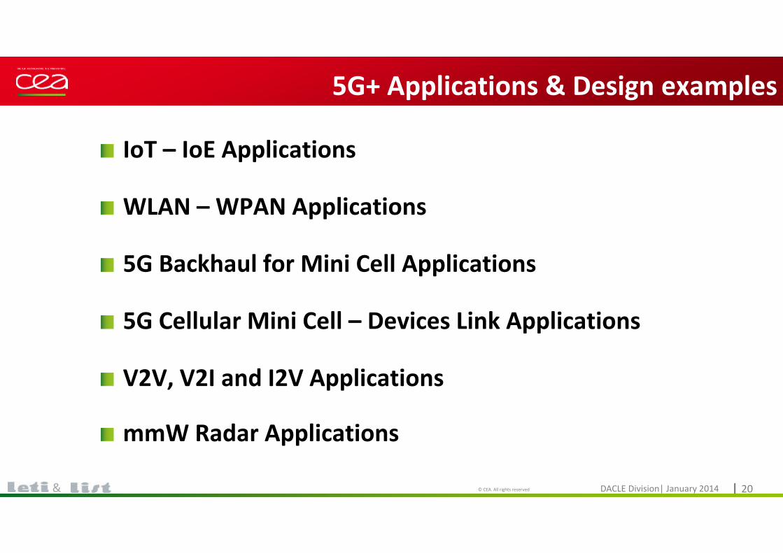
5G+ Applications & Design examples
IoT – IoE Applications
WLAN – WPAN Applications
5G Backhaul for Mini Cell Applications
5G Cellular Mini Cell – Devices Link Applications
V2V, V2I and I2V Applications
mmW Radar Applications
Cliquez pour modifier le style du titre
DACLE Division| January 2014© CEA. All rights reserved | 21&
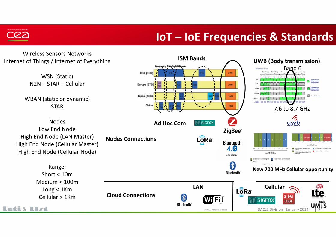
IoT – IoE Frequencies & StandardsWireless Sensors Networks
Internet of Things / Internet of Everything
WSN (Static)N2N – STAR – Cellular
WBAN (static or dynamic)STAR
NodesLow End Node
High End Node (LAN Master)High End Node (Cellular Master)High End Node (Cellular Node)
Range:Short < 10m
Medium < 100mLong < 1Km
Cellular > 1Km
Band 6
7.6 to 8.7 GHz
UWB (Body transmission)ISM Bands
Ad Hoc Com
Nodes Connections
Cloud ConnectionsLAN Cellular
New 700 MHz Cellular opportunity
Cliquez pour modifier le style du titre
DACLE Division| January 2014© CEA. All rights reserved | 22&
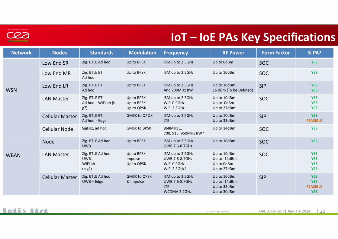
IoT – IoE PAs Key SpecificationsNetwork Nodes Standards Modulation Frequency RF Power Form Factor Si PA?
WSN
Low End SR Zig. BTLE Ad hoc Up to BPSK ISM up to 2.5GHz Up to 0dBm SOC YES
Low End MR Zig. BTLE BT Ad hoc
Up to BPSK ISM up to 2.5GHz Up to 10dBm SOC YES
Low End LR Zig. BTLE BT Ad hoc
Up to BPSK ISM up to 2.5GHzAnd 700MHz BW
Up to 10dBm16 dBm (To be Defined)
SIP YESYES
LAN Master Zig. BTLE BT Ad hoc – WiFi ah (b g?)
Up to BPSKUp to BPSKUp to QPSK
ISM up to 2.5GHzWiFi 0.9GHz WiFi 2.5GHz
Up to 10dBmUp to 0dBmUp to 27dBm
SOC YESYESYES
Cellular Master Zig. BTLE BT Ad hoc ‐ Edge
GMSK to QPQK ISM up to 2.5GHzLTE
Up to 10dBmUp to 33dBm
SIP YESFEASIBLE
Cellular Node SigFox, ad hoc GMSK to BPSK 868MHz … 700, 915, 950MHz BW?
Up to 14dBm SOC YES
WBAN
Node Zig. BTLE Ad hocUWB
Up to BPSK ISM up to 2.5GHzUWB 7.6‐8.7GHz
Up to 10dBm SOC YES
LAN Master Zig. BTLE Ad hocUWB –WiFi ah (b g?)
Up to BPSKImpulseUp to QPSK
ISM up to 2.5GHzUWB 7.6‐8.7GHzWiFi 0.9GHzWiFi 2.5GHz?
Up to 10dBmUp to ‐14dBmUp to 0dBmUp to 27dBm
SOC YESYESYESYES
Cellular Master Zig. BTLE Ad hocUWB – Edge
GMSK to QPSK& Impulse
ISM up to 2.5GHzUWB 7.6‐8.7GHzLTEWCDMA 2.2GHz
Up to 10dBmUp to ‐14dBmUp to 33dBmUp to 30dBm
SIP YESYES
FEASIBLEYES
Cliquez pour modifier le style du titre
DACLE Division| January 2014© CEA. All rights reserved | 23&
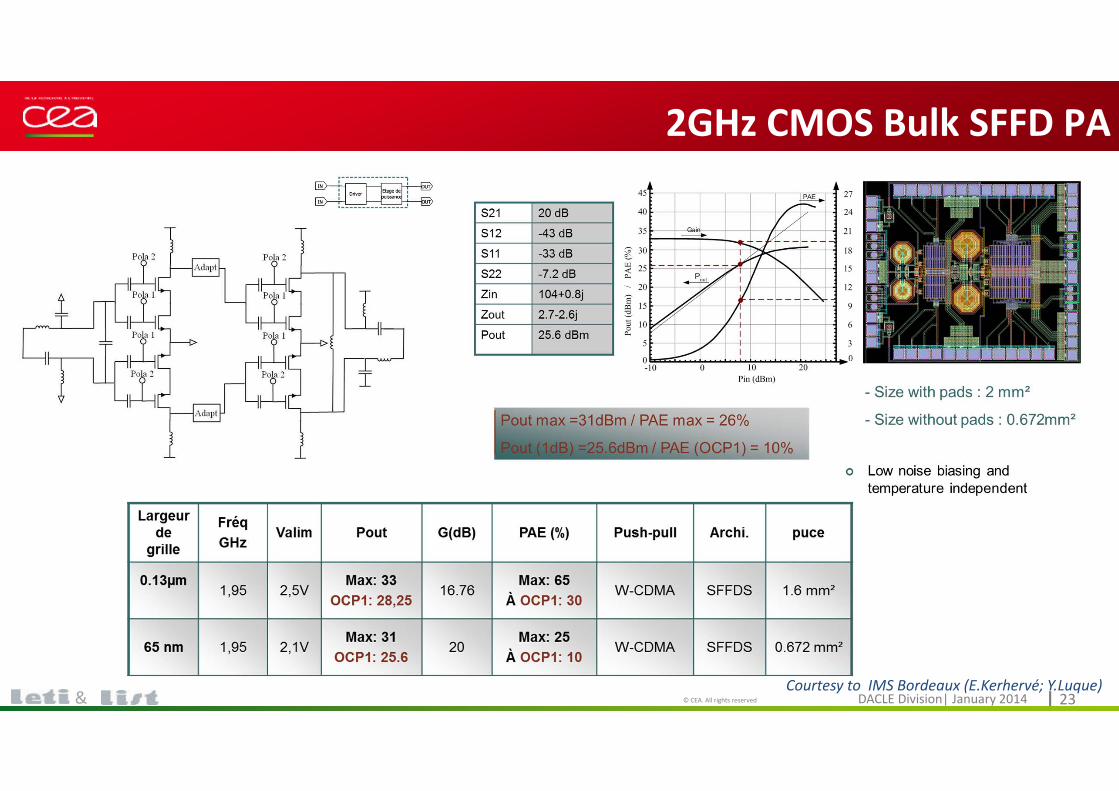
2GHz CMOS Bulk SFFD PA
Courtesy to IMS Bordeaux (E.Kerhervé; Y.Luque)
Cliquez pour modifier le style du titre
DACLE Division| January 2014© CEA. All rights reserved | 24&
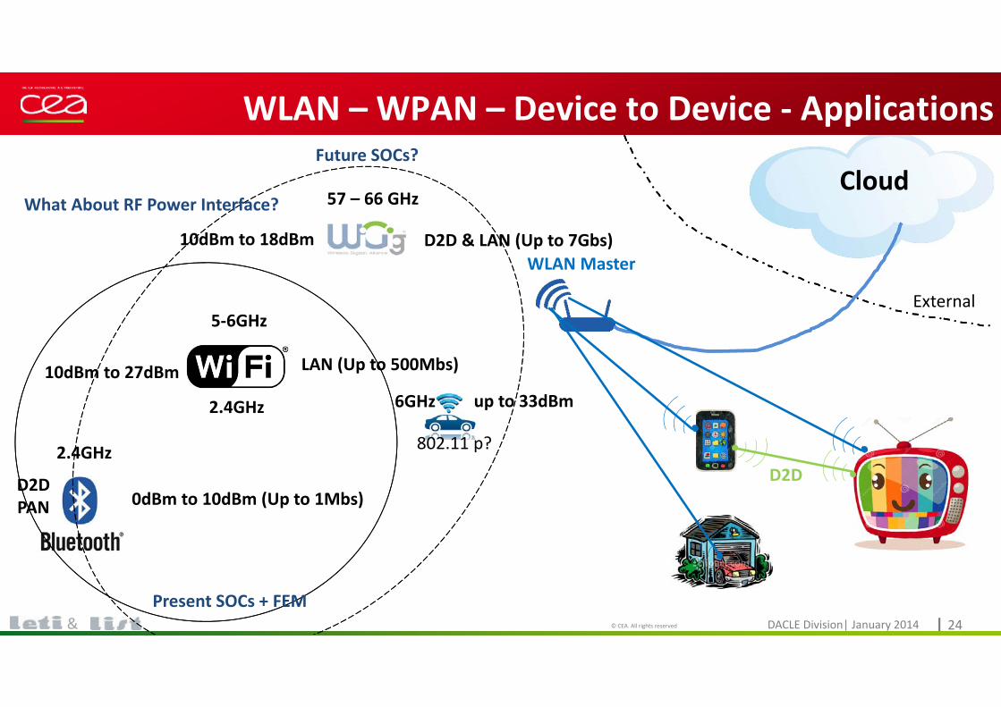
WLAN – WPAN – Device to Device ‐ Applications
Cloud
External
WLAN Master
D2D2.4GHz
5‐6GHz
2.4GHz
57 – 66 GHz
D2DPAN
LAN (Up to 500Mbs)
D2D & LAN (Up to 7Gbs)
0dBm to 10dBm (Up to 1Mbs)
10dBm to 27dBm
10dBm to 18dBm
Present SOCs + FEM
Future SOCs?
What About RF Power Interface?
802.11 p?
6GHz up to 33dBm
Cliquez pour modifier le style du titre
DACLE Division| January 2014© CEA. All rights reserved | 25&
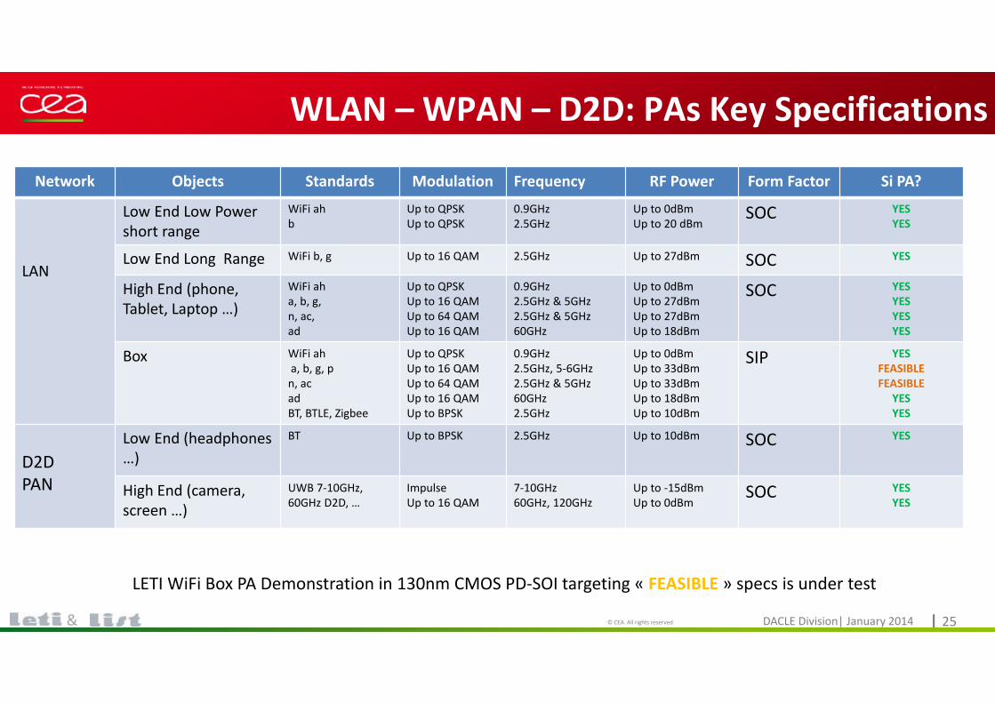
WLAN – WPAN – D2D: PAs Key Specifications
Network Objects Standards Modulation Frequency RF Power Form Factor Si PA?
LAN
Low End Low Powershort range
WiFi ahb
Up to QPSKUp to QPSK
0.9GHz2.5GHz
Up to 0dBmUp to 20 dBm
SOC YESYES
Low End Long Range WiFi b, g Up to 16 QAM 2.5GHz Up to 27dBm SOC YES
High End (phone, Tablet, Laptop …)
WiFi aha, b, g, n, ac, ad
Up to QPSKUp to 16 QAMUp to 64 QAMUp to 16 QAM
0.9GHz2.5GHz & 5GHz2.5GHz & 5GHz60GHz
Up to 0dBmUp to 27dBmUp to 27dBmUp to 18dBm
SOC YESYESYESYES
Box WiFi aha, b, g, p n, acadBT, BTLE, Zigbee
Up to QPSKUp to 16 QAMUp to 64 QAMUp to 16 QAMUp to BPSK
0.9GHz2.5GHz, 5‐6GHz2.5GHz & 5GHz60GHz2.5GHz
Up to 0dBmUp to 33dBmUp to 33dBmUp to 18dBmUp to 10dBm
SIP YESFEASIBLEFEASIBLE
YESYES
D2D PAN
Low End (headphones…)
BT Up to BPSK 2.5GHz Up to 10dBm SOC YES
High End (camera, screen …)
UWB 7‐10GHz,60GHz D2D, …
ImpulseUp to 16 QAM
7‐10GHz60GHz, 120GHz
Up to ‐15dBmUp to 0dBm
SOC YESYES
LETI WiFi Box PA Demonstration in 130nm CMOS PD‐SOI targeting « FEASIBLE » specs is under test
Cliquez pour modifier le style du titre
DACLE Division| January 2014© CEA. All rights reserved | 26&
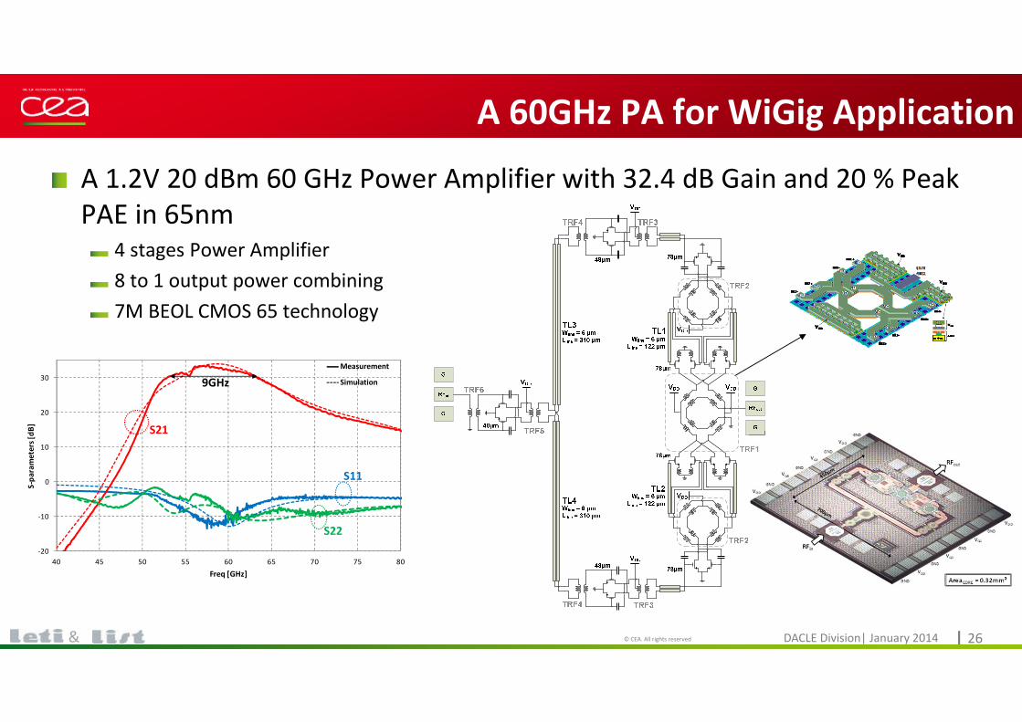
A 60GHz PA for WiGig Application
A 1.2V 20 dBm 60 GHz Power Amplifier with 32.4 dB Gain and 20 % Peak PAE in 65nm
4 stages Power Amplifier8 to 1 output power combining7M BEOL CMOS 65 technology
‐20
‐10
0
10
20
30
40 45 50 55 60 65 70 75 80
S‐pa
rameters [dB
]
Freq [GHz]
S21
S22
S11
9GHzMeasurement
Simulation
Cliquez pour modifier le style du titre
DACLE Division| January 2014© CEA. All rights reserved | 27&
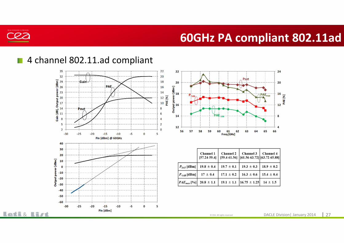
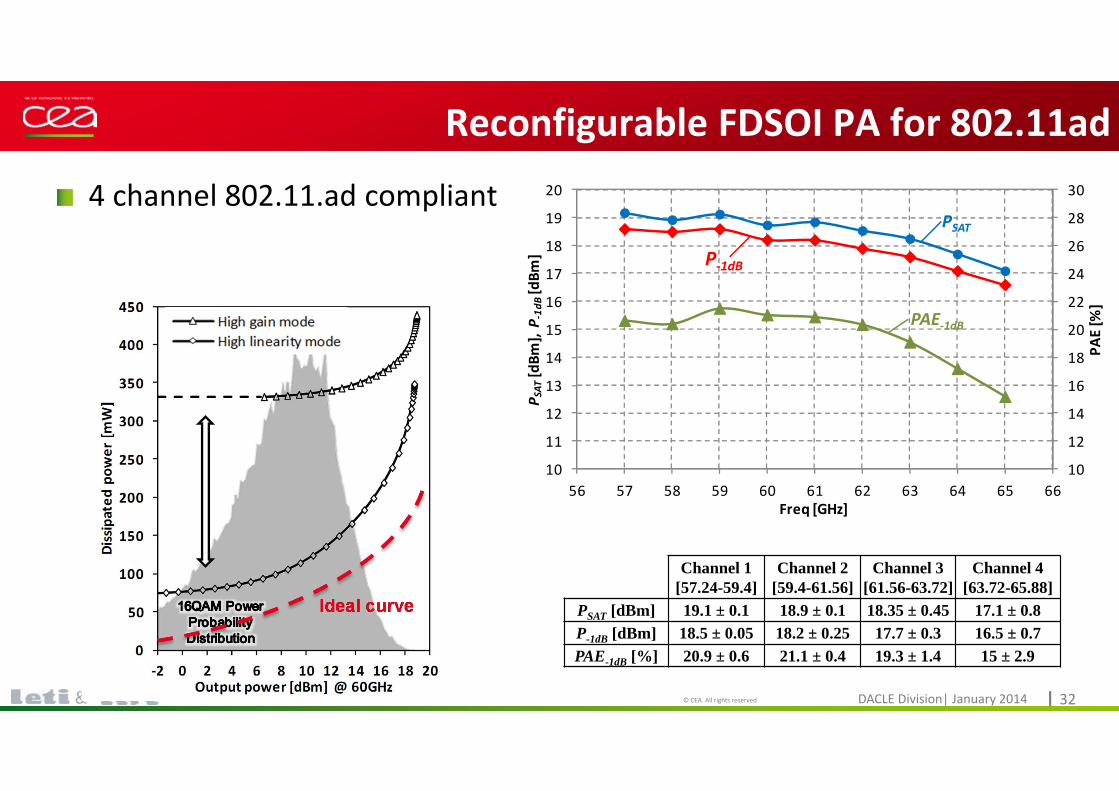
60GHz PA compliant 802.11ad
4 channel 802.11.ad compliant
Cliquez pour modifier le style du titre
DACLE Division| January 2014© CEA. All rights reserved | 28&
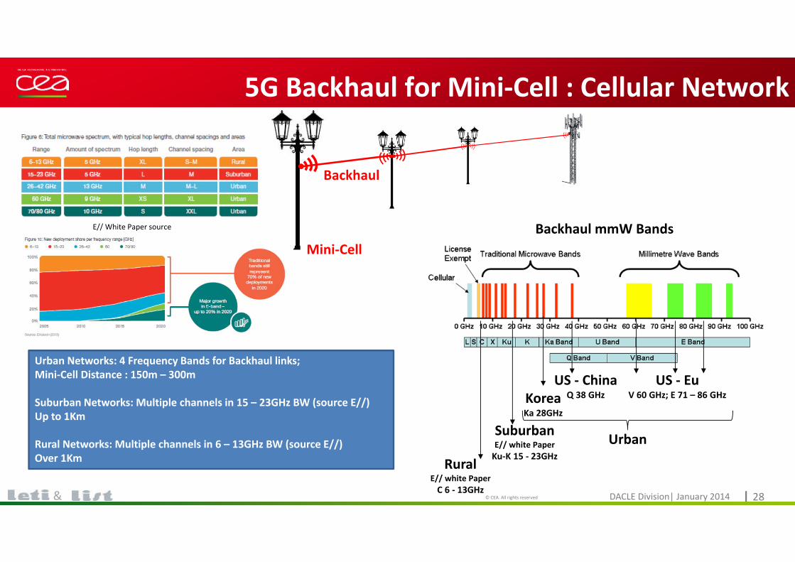
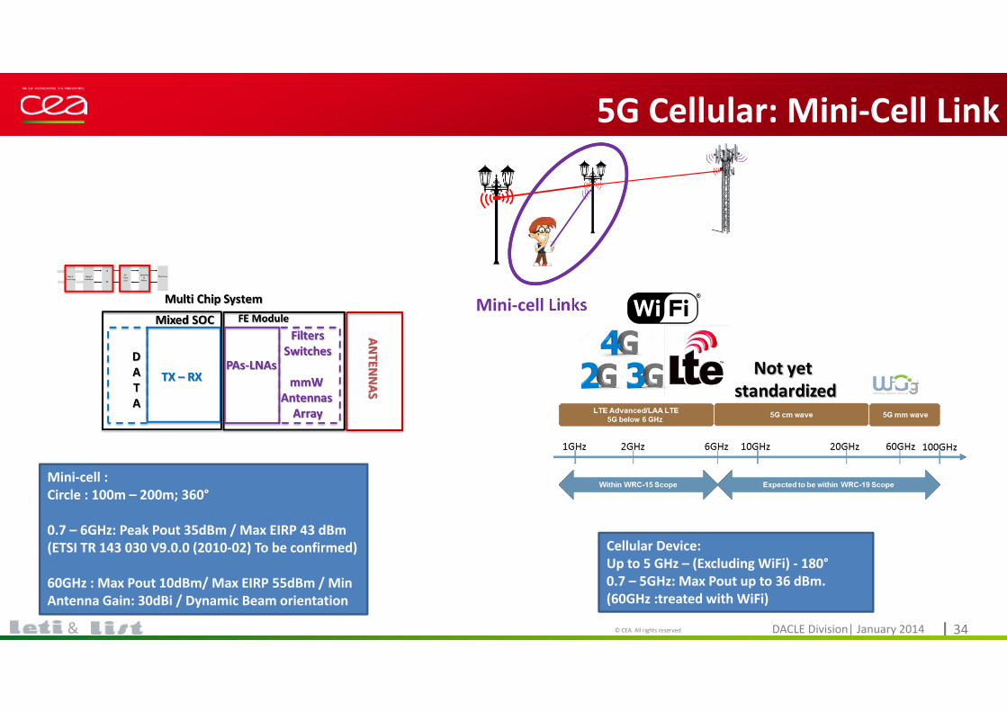
5G Backhaul for Mini‐Cell : Cellular Network
Backhaul
Mini‐CellBackhaul mmW Bands
KoreaKa 28GHz
US ‐ ChinaQ 38 GHz
US ‐ EuV 60 GHz; E 71 – 86 GHz
Urban Networks: 4 Frequency Bands for Backhaul links;Mini‐Cell Distance : 150m – 300m
Suburban Networks: Multiple channels in 15 – 23GHz BW (source E//)Up to 1Km
Rural Networks: Multiple channels in 6 – 13GHz BW (source E//)Over 1Km Rural
E// white PaperC 6 ‐ 13GHz
SuburbanE// white PaperKu‐K 15 ‐ 23GHz
Urban
E// White Paper source
Cliquez pour modifier le style du titre
DACLE Division| January 2014© CEA. All rights reserved | 29&
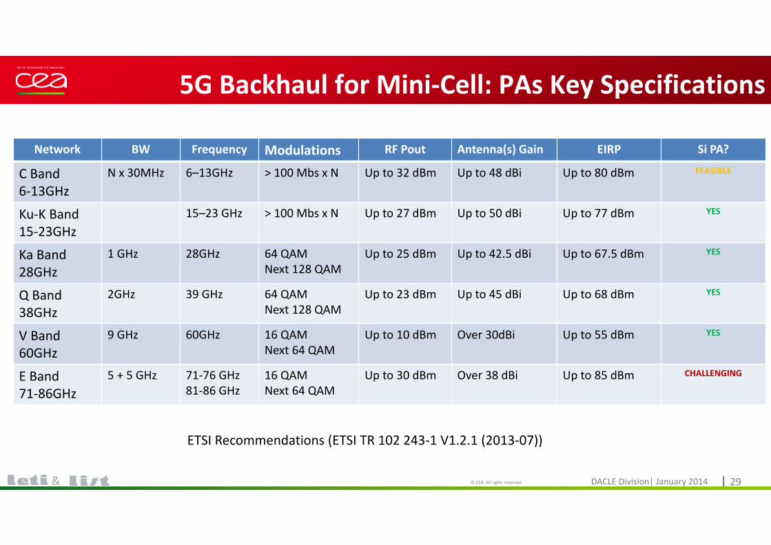
5G Backhaul for Mini‐Cell: PAs Key Specifications
Network BW Frequency Modulations RF Pout Antenna(s) Gain EIRP Si PA?
C Band6‐13GHz
N x 30MHz 6–13GHz > 100 Mbs x N Up to 32 dBm Up to 48 dBi Up to 80 dBm FEASIBLE
Ku‐K Band15‐23GHz
15–23 GHz > 100 Mbs x N Up to 27 dBm Up to 50 dBi Up to 77 dBm YES
Ka Band28GHz
1 GHz 28GHz 64 QAM Next 128 QAM
Up to 25 dBm Up to 42.5 dBi Up to 67.5 dBm YES
Q Band38GHz
2GHz 39 GHz 64 QAM Next 128 QAM
Up to 23 dBm Up to 45 dBi Up to 68 dBm YES
V Band60GHz
9 GHz 60GHz 16 QAMNext 64 QAM
Up to 10 dBm Over 30dBi Up to 55 dBm YES
E Band71‐86GHz
5 + 5 GHz 71‐76 GHz81‐86 GHz
16 QAMNext 64 QAM
Up to 30 dBm Over 38 dBi Up to 85 dBm CHALLENGING
ETSI Recommendations (ETSI TR 102 243‐1 V1.2.1 (2013‐07))
Cliquez pour modifier le style du titre
DACLE Division| January 2014© CEA. All rights reserved | 30&
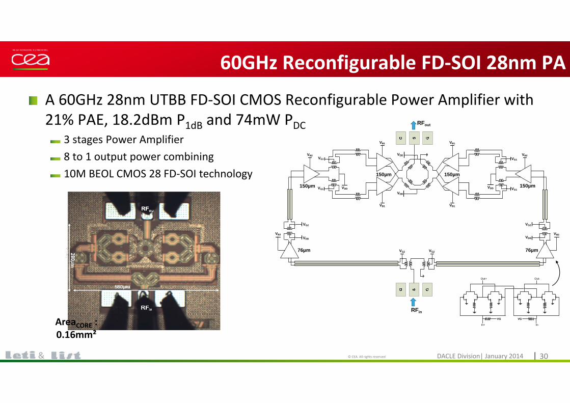
60GHz Reconfigurable FD‐SOI 28nm PA
A 60GHz 28nm UTBB FD‐SOI CMOS Reconfigurable Power Amplifier with 21% PAE, 18.2dBm P1dB and 74mW PDC
3 stages Power Amplifier8 to 1 output power combining10M BEOL CMOS 28 FD‐SOI technology
VDD
VDDVG1
VG1 VDD
VB2
VG1VDD
VG1
VB2
VB1
VB1 VB1
VB1
VDDVDD
VB2 VB2
VG2 VG2
VG2 VG2
Out+ Out-
In+ In-
VG VG
RFin
RFout
150µm150µm
150µm 150µm
76µm76µm
AreaCORE :0.16mm²
Cliquez pour modifier le style du titre
DACLE Division| January 2014© CEA. All rights reserved | 31&
PA Reconfigurability
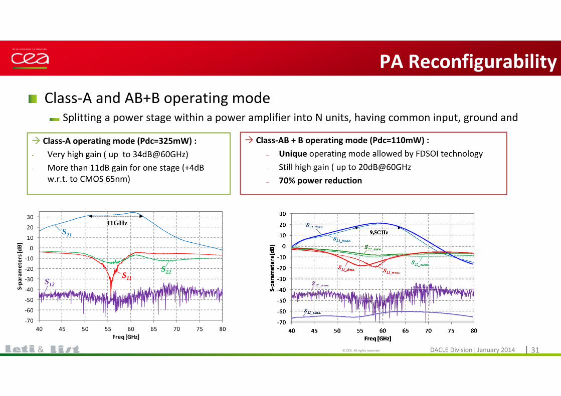
Class‐A and AB+B operating modeSplitting a power stage within a power amplifier into N units, having common input, ground and
‐70
‐60
‐50
‐40
‐30
‐20
‐10
0
10
20
30
40 45 50 55 60 65 70 75 80
S‐parameters [dB
]
Freq [GHz]
S21
S11S22
S12
11GHz
Class‐A operating mode (Pdc=325mW) : ‐ Very high gain ( up to 34dB@60GHz)‐ More than 11dB gain for one stage (+4dB
w.r.t. to CMOS 65nm)
Class‐AB + B operating mode (Pdc=110mW) : — Unique operating mode allowed by FDSOI technology— Still high gain ( up to 20dB@60GHz— 70% power reduction
Cliquez pour modifier le style du titre
DACLE Division| January 2014© CEA. All rights reserved | 32&
Reconfigurable FDSOI PA for 802.11ad
4 channel 802.11.ad compliant
10
12
14
16
18
20
22
24
26
28
30
10
11
12
13
14
15
16
17
18
19
20
56 57 58 59 60 61 62 63 64 65 66
PAE [%
]
P SAT[dBm
], P ‐
1dB[dBm
]
Freq [GHz]
PAE‐1dB
P‐1dB
PSAT
Channel 1[57.24-59.4]
Channel 2[59.4-61.56]
Channel 3[61.56-63.72]
Channel 4[63.72-65.88]
PSAT [dBm] 19.1 ± 0.1 18.9 ± 0.1 18.35 ± 0.45 17.1 ± 0.8P-1dB [dBm] 18.5 ± 0.05 18.2 ± 0.25 17.7 ± 0.3 16.5 ± 0.7PAE-1dB [%] 20.9 ± 0.6 21.1 ± 0.4 19.3 ± 1.4 15 ± 2.9
Cliquez pour modifier le style du titre
DACLE Division| January 2014© CEA. All rights reserved | 33&
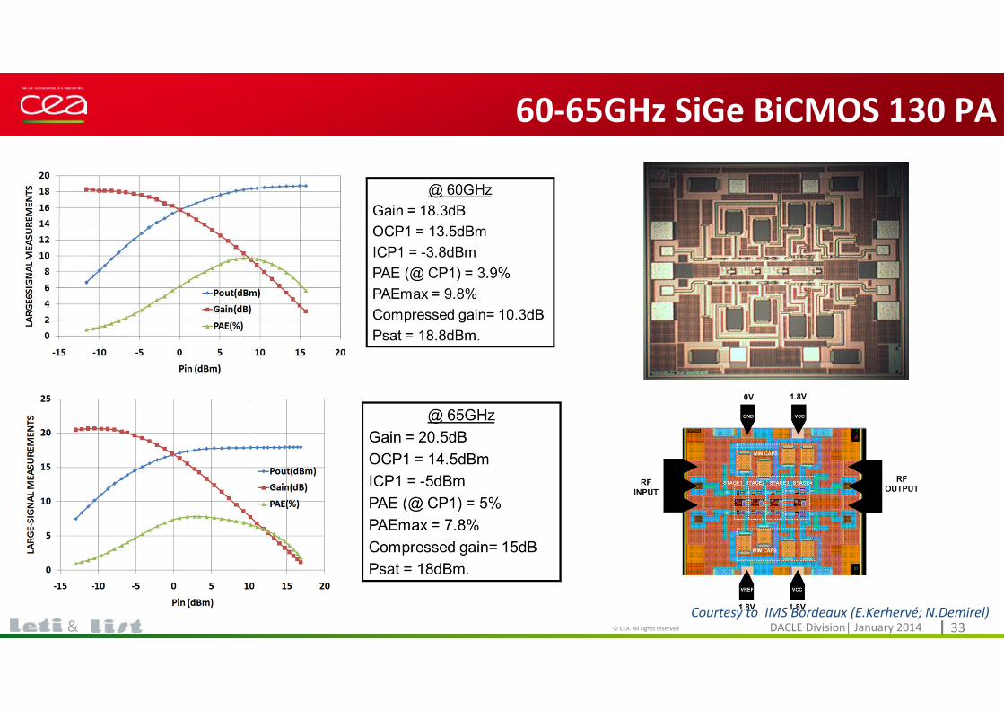
60‐65GHz SiGe BiCMOS 130 PA
Courtesy to IMS Bordeaux (E.Kerhervé; N.Demirel)
Cliquez pour modifier le style du titre
DACLE Division| January 2014© CEA. All rights reserved | 34&
5G Cellular: Mini‐Cell Link
Mini‐cell Links
Mini‐cell :Circle : 100m – 200m; 360°
0.7 – 6GHz: Peak Pout 35dBm / Max EIRP 43 dBm(ETSI TR 143 030 V9.0.0 (2010‐02) To be confirmed)
60GHz : Max Pout 10dBm/ Max EIRP 55dBm / Min Antenna Gain: 30dBi / Dynamic Beam orientation
Cellular Device: Up to 5 GHz – (Excluding WiFi) ‐ 180°0.7 – 5GHz: Max Pout up to 36 dBm. (60GHz :treated with WiFi)
Cliquez pour modifier le style du titre
DACLE Division| January 2014© CEA. All rights reserved | 35&
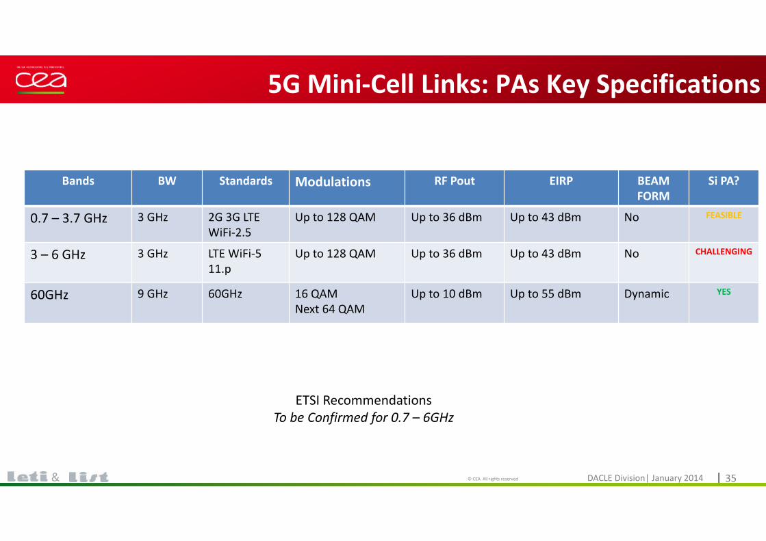
5G Mini‐Cell Links: PAs Key Specifications
Bands BW Standards Modulations RF Pout EIRP BEAM FORM
Si PA?
0.7 – 3.7 GHz 3 GHz 2G 3G LTE WiFi‐2.5
Up to 128 QAM Up to 36 dBm Up to 43 dBm No FEASIBLE
3 – 6 GHz 3 GHz LTE WiFi‐511.p
Up to 128 QAM Up to 36 dBm Up to 43 dBm No CHALLENGING
60GHz 9 GHz 60GHz 16 QAMNext 64 QAM
Up to 10 dBm Up to 55 dBm Dynamic YES
ETSI RecommendationsTo be Confirmed for 0.7 – 6GHz
Cliquez pour modifier le style du titre
DACLE Division| January 2014© CEA. All rights reserved | 36&
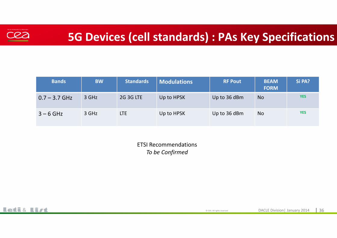
5G Devices (cell standards) : PAs Key Specifications
Bands BW Standards Modulations RF Pout BEAM FORM
Si PA?
0.7 – 3.7 GHz 3 GHz 2G 3G LTE Up to HPSK Up to 36 dBm No YES
3 – 6 GHz 3 GHz LTE Up to HPSK Up to 36 dBm No YES
ETSI RecommendationsTo be Confirmed
Cliquez pour modifier le style du titre
DACLE Division| January 2014© CEA. All rights reserved | 37& Giry Alexandre | March 2017
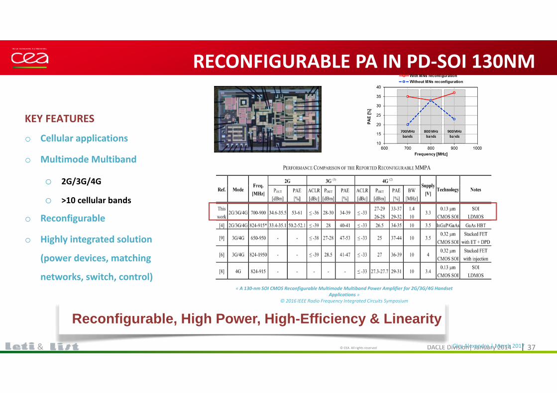
RECONFIGURABLE PA IN PD‐SOI 130NM
Reconfigurable, High Power, High-Efficiency & Linearity
« A 130‐nm SOI CMOS Reconfigurable Multimode Multiband Power Amplifier for 2G/3G/4G HandsetApplications »
© 2016 IEEE Radio Frequency Integrated Circuits Symposium
KEY FEATURES
o Cellular applications
o Multimode Multiband
o 2G/3G/4G
o >10 cellular bands
o Reconfigurable
o Highly integrated solution
(power devices, matching
networks, switch, control)
Cliquez pour modifier le style du titre
DACLE Division| January 2014© CEA. All rights reserved | 38&
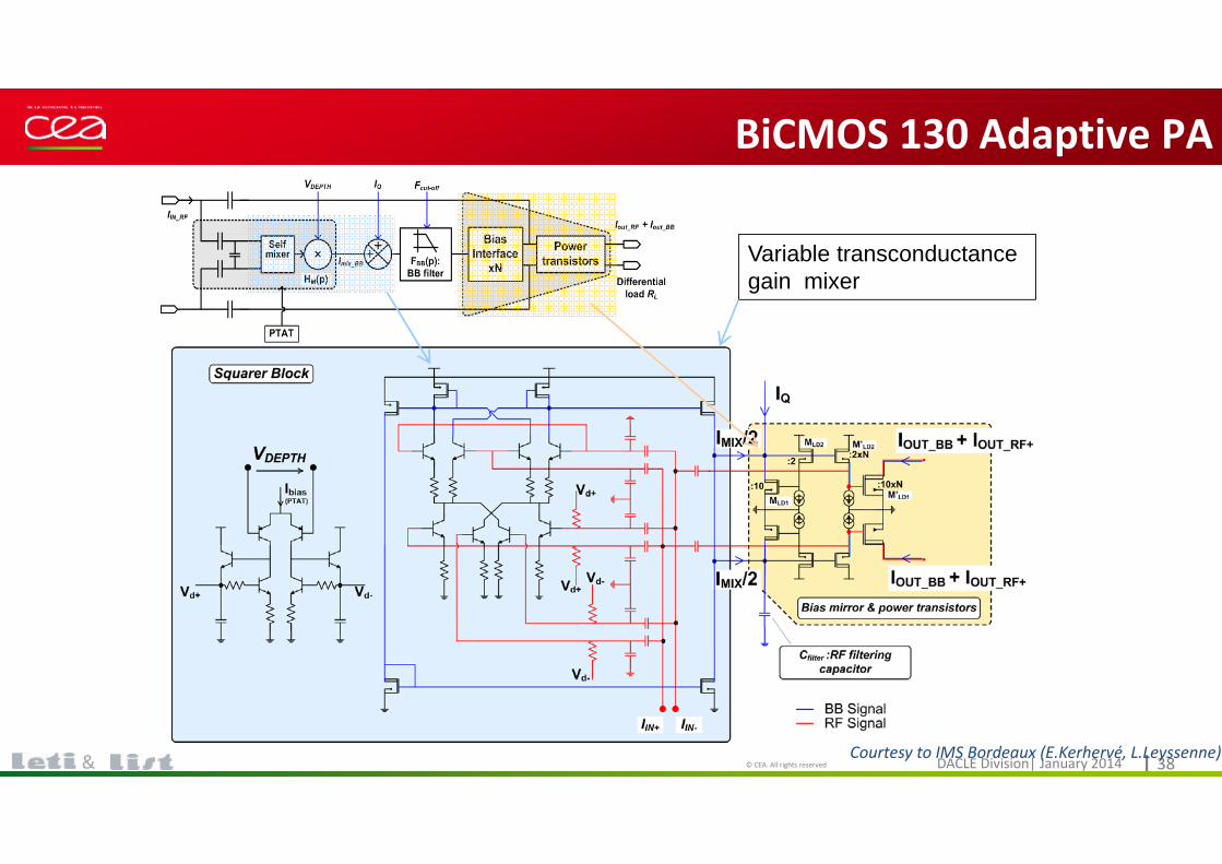
BiCMOS 130 Adaptive PA
Variable transconductance gain mixer
Courtesy to IMS Bordeaux (E.Kerhervé, L.Leyssenne)
Cliquez pour modifier le style du titre
DACLE Division| January 2014© CEA. All rights reserved | 39&
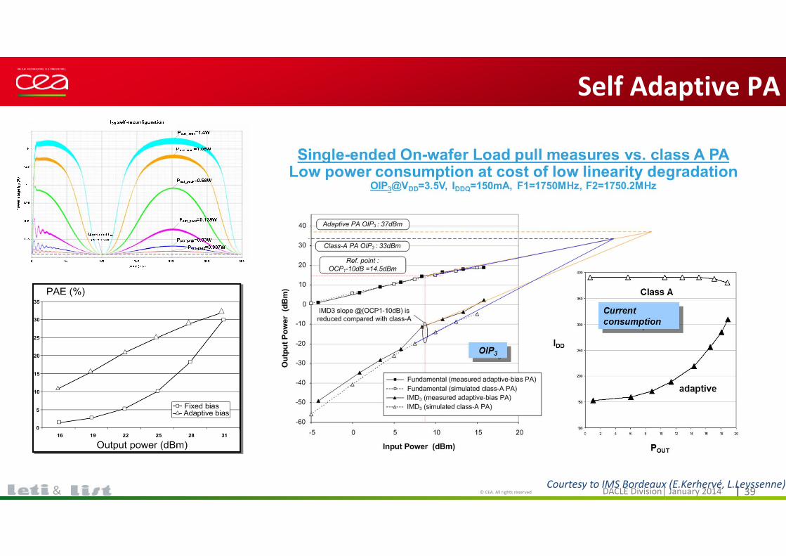
Self Adaptive PA
Courtesy to IMS Bordeaux (E.Kerhervé, L.Leyssenne)
Cliquez pour modifier le style du titre
DACLE Division| January 2014© CEA. All rights reserved | 40&
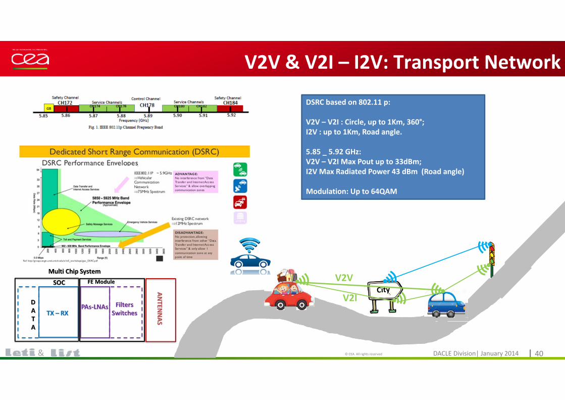
V2V & V2I – I2V: Transport Network
V2V
V2I
DSRC based on 802.11 p:
V2V – V2I : Circle, up to 1Km, 360°; I2V : up to 1Km, Road angle.
5.85 _ 5.92 GHz: V2V – V2I Max Pout up to 33dBm; I2V Max Radiated Power 43 dBm (Road angle)
Modulation: Up to 64QAM
Cliquez pour modifier le style du titre
DACLE Division| January 2014© CEA. All rights reserved | 41&
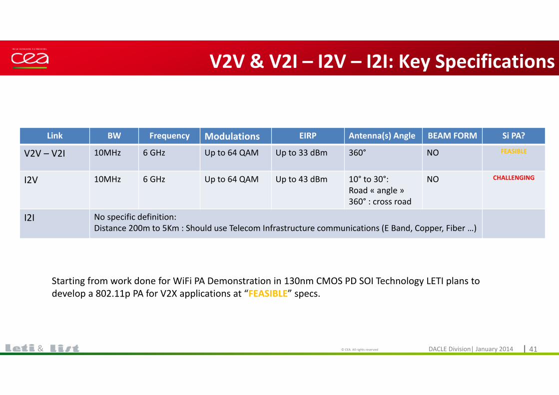
V2V & V2I – I2V – I2I: Key Specifications
Link BW Frequency Modulations EIRP Antenna(s) Angle BEAM FORM Si PA?
V2V – V2I 10MHz 6 GHz Up to 64 QAM Up to 33 dBm 360° NO FEASIBLE
I2V 10MHz 6 GHz Up to 64 QAM Up to 43 dBm 10° to 30°:Road « angle »360° : cross road
NO CHALLENGING
I2I No specific definition:Distance 200m to 5Km : Should use Telecom Infrastructure communications (E Band, Copper, Fiber …)
Starting from work done for WiFi PA Demonstration in 130nm CMOS PD SOI Technology LETI plans to develop a 802.11p PA for V2X applications at “FEASIBLE” specs.
Cliquez pour modifier le style du titre
DACLE Division| January 2014© CEA. All rights reserved | 42&
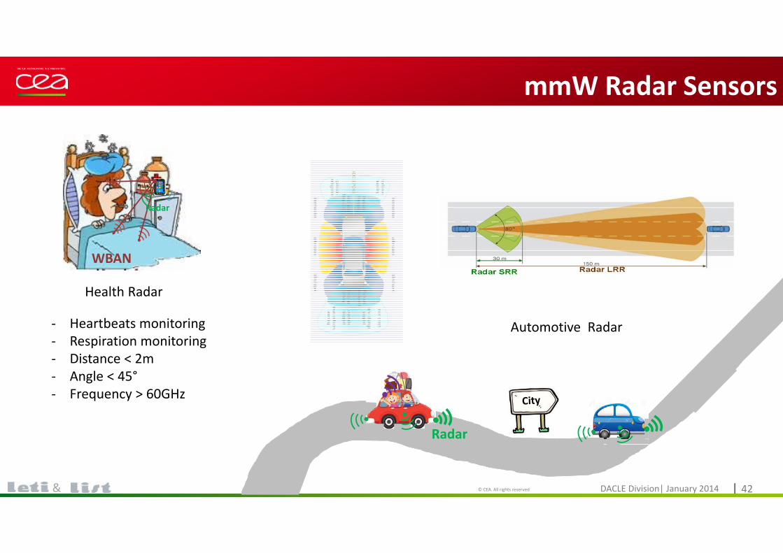
mmW Radar Sensors
Radar
WBAN
Radar
Health Radar
Automotive Radar‐ Heartbeats monitoring ‐ Respiration monitoring‐ Distance < 2m‐ Angle < 45°‐ Frequency > 60GHz
Cliquez pour modifier le style du titre
DACLE Division| January 2014© CEA. All rights reserved | 43&
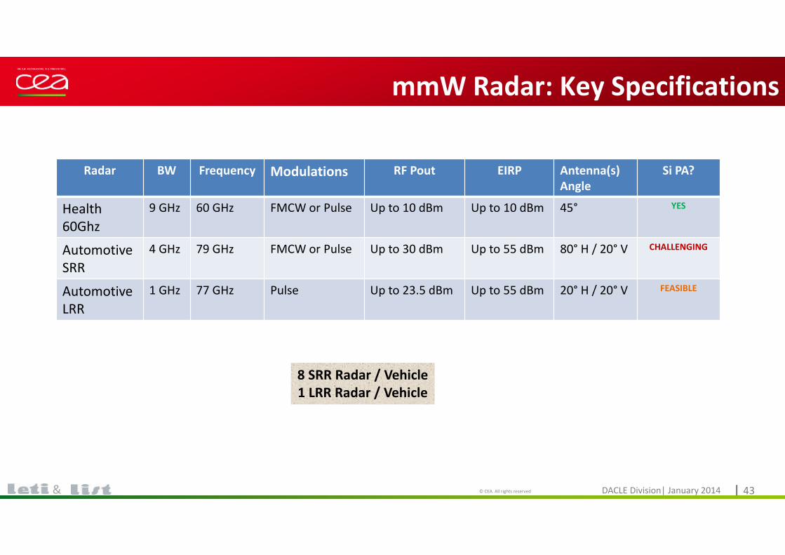
mmW Radar: Key Specifications
Radar BW Frequency Modulations RF Pout EIRP Antenna(s)Angle
Si PA?
Health 60Ghz
9 GHz 60 GHz FMCW or Pulse Up to 10 dBm Up to 10 dBm 45° YES
Automotive SRR
4 GHz 79 GHz FMCW or Pulse Up to 30 dBm Up to 55 dBm 80° H / 20° V CHALLENGING
Automotive LRR
1 GHz 77 GHz Pulse Up to 23.5 dBm Up to 55 dBm 20° H / 20° V FEASIBLE
8 SRR Radar / Vehicle1 LRR Radar / Vehicle
Cliquez pour modifier le style du titre
DACLE Division| January 2014© CEA. All rights reserved | 44&
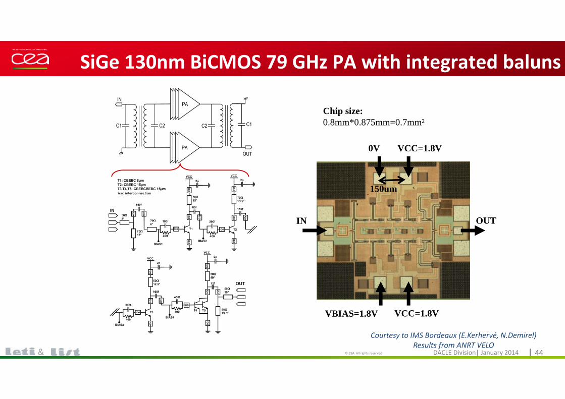
SiGe 130nm BiCMOS 79 GHz PA with integrated baluns
IN OUT
VCC=1.8V0V
VCC=1.8VVBIAS=1.8V
150um
Chip size:0.8mm*0.875mm=0.7mm²
Courtesy to IMS Bordeaux (E.Kerhervé, N.Demirel)Results from ANRT VELO
Cliquez pour modifier le style du titre
DACLE Division| January 2014© CEA. All rights reserved | 45&
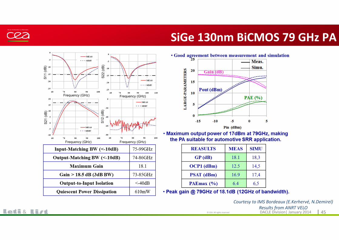
SiGe 130nm BiCMOS 79 GHz PA
Courtesy to IMS Bordeaux (E.Kerhervé, N.Demirel)Results from ANRT VELO
Cliquez pour modifier le style du titre
DACLE Division| January 2014© CEA. All rights reserved | 46&
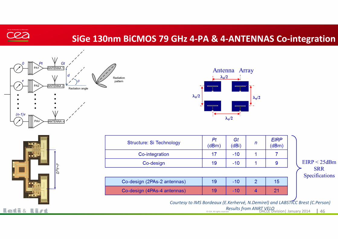
SiGe 130nm BiCMOS 79 GHz 4‐PA & 4‐ANTENNAS Co‐integration
Courtesy to IMS Bordeaux (E.Kerhervé, N.Demirel) and LABSTICC Brest (C.Person)Results from ANRT VELO
Cliquez pour modifier le style du titre
DACLE Division| January 2014© CEA. All rights reserved | 47&
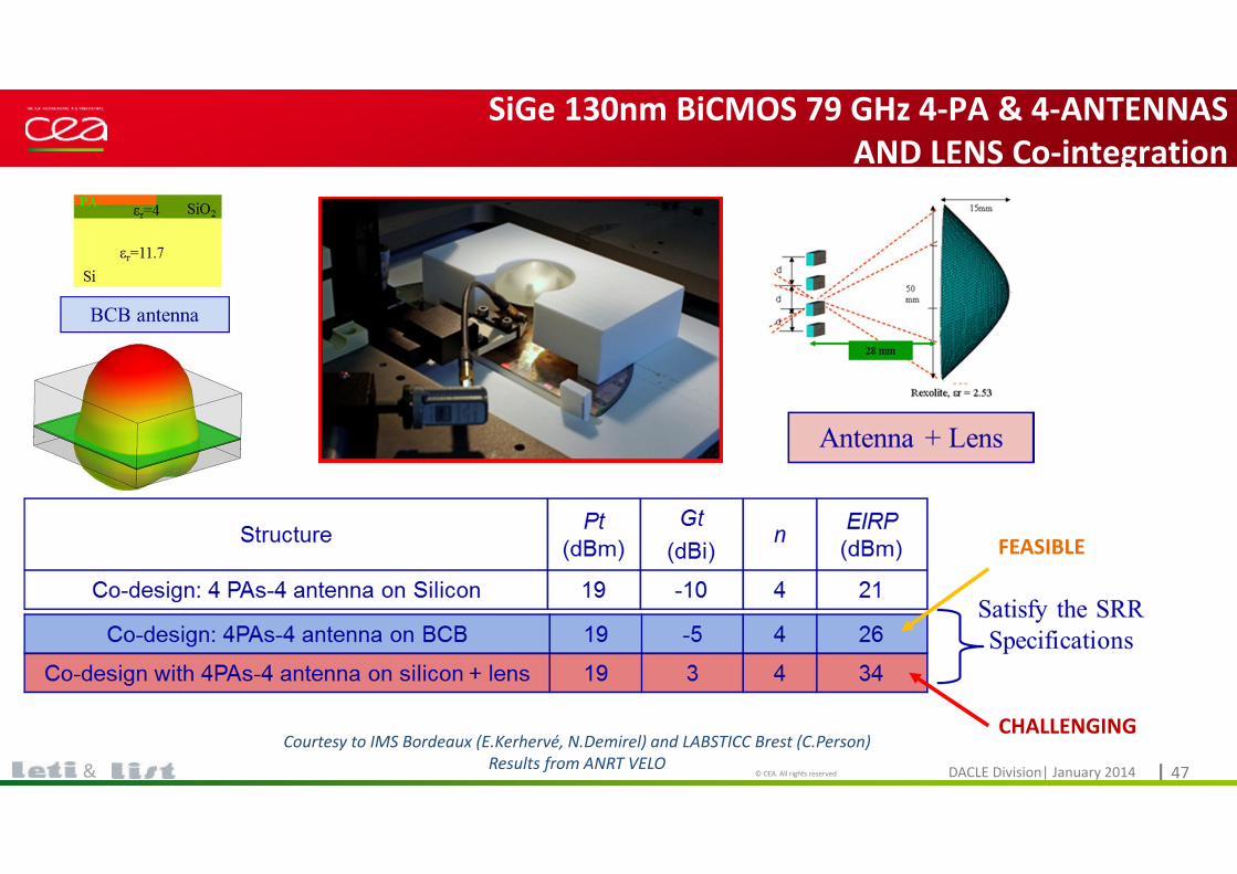
SiGe 130nm BiCMOS 79 GHz 4‐PA & 4‐ANTENNAS AND LENS Co‐integration
Courtesy to IMS Bordeaux (E.Kerhervé, N.Demirel) and LABSTICC Brest (C.Person)Results from ANRT VELO
CHALLENGING
FEASIBLE
Cliquez pour modifier le style du titre
DACLE Division| January 2014© CEA. All rights reserved | 48&
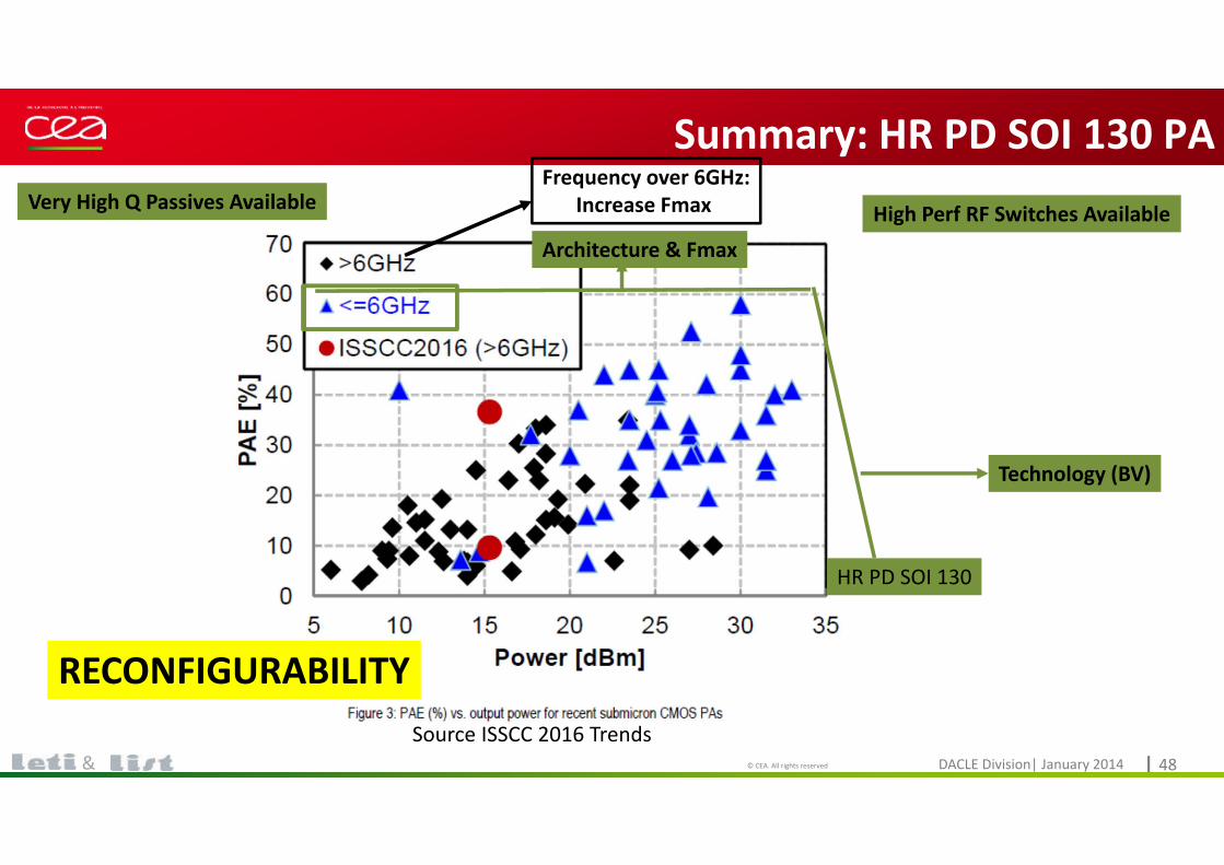
Summary: HR PD SOI 130 PA
HR PD SOI 130
Architecture & Fmax
Technology (BV)
Frequency over 6GHz:Increase Fmax
Source ISSCC 2016 Trends
High Perf RF Switches AvailableVery High Q Passives Available
RECONFIGURABILITY
Cliquez pour modifier le style du titre
DACLE Division| January 2014© CEA. All rights reserved | 49&
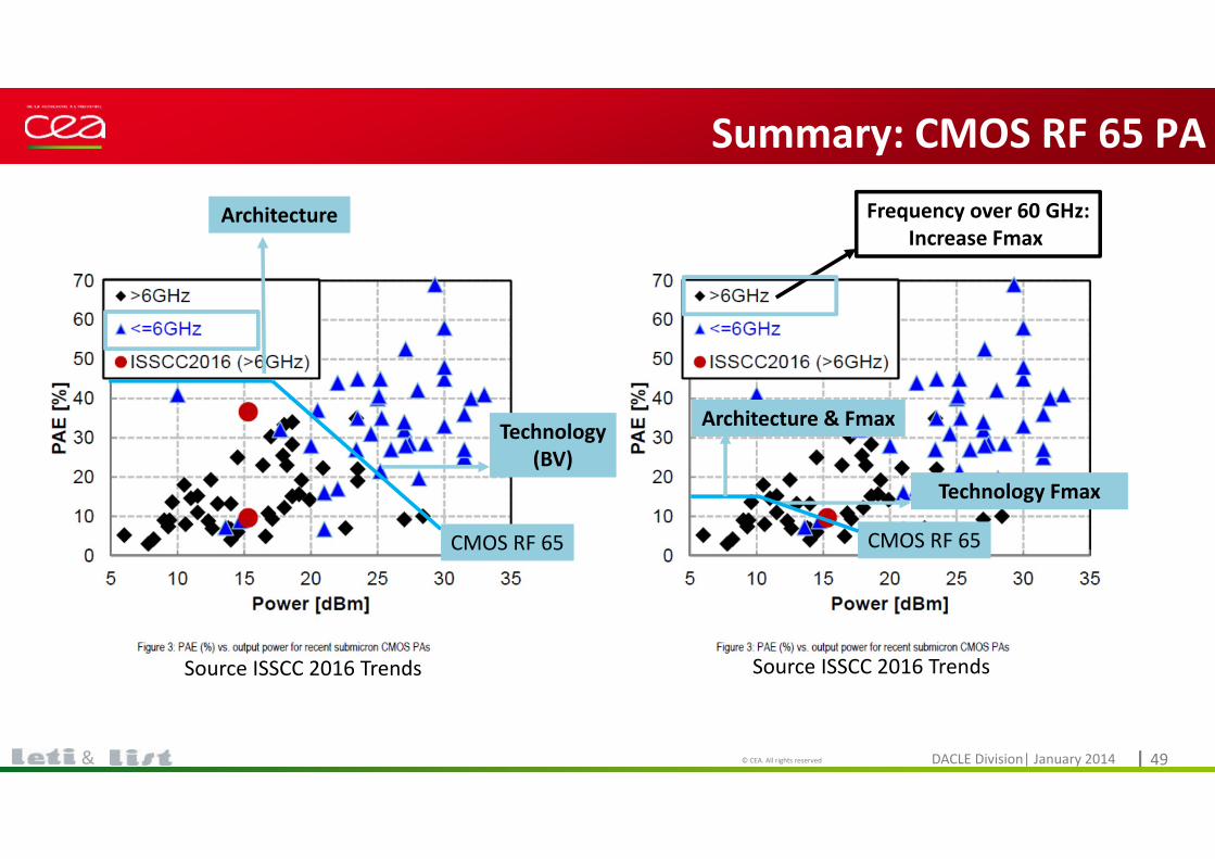
Summary: CMOS RF 65 PA
CMOS RF 65
Architecture
Technology(BV)
Frequency over 60 GHz:Increase Fmax
Source ISSCC 2016 Trends
CMOS RF 65
Architecture & Fmax
Technology Fmax
Source ISSCC 2016 Trends
Cliquez pour modifier le style du titre
DACLE Division| January 2014© CEA. All rights reserved | 50&
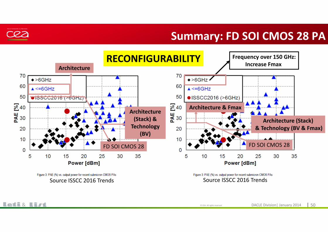
Summary: FD SOI CMOS 28 PA
FD SOI CMOS 28
Architecture
Architecture (Stack) & Technology
(BV)
Frequency over 150 GHz:Increase Fmax
Source ISSCC 2016 Trends
FD SOI CMOS 28
Architecture & Fmax
Architecture (Stack)& Technology (BV & Fmax)
Source ISSCC 2016 Trends
RECONFIGURABILITY
Cliquez pour modifier le style du titre
DACLE Division| January 2014© CEA. All rights reserved | 51&
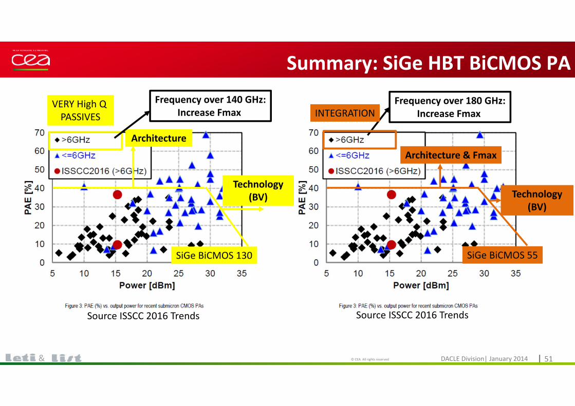
Summary: SiGe HBT BiCMOS PA
SiGe BiCMOS 130
Architecture
Technology(BV)
Frequency over 180 GHz:Increase Fmax
Source ISSCC 2016 Trends
SiGe BiCMOS 55
Architecture & Fmax
Technology(BV)
Source ISSCC 2016 Trends
Frequency over 140 GHz:Increase Fmax INTEGRATION
VERY High Q PASSIVES
Cliquez pour modifier le style du titre
DACLE Division| January 2014© CEA. All rights reserved | 52&
Conclusions
CMOS and SiGe BiCMOS technologies allow designing PA for Connectivity Applications.
RF CMOS 65 processes are well adapted for SOC low power output, (up to 10 dBm) connectivity applications with operating frequencies up to 60GHz.FD SOI CMOS 28 processes are well adapted for SOC low to medium power output, (up to 20 dBm) RECONFIGURABLE connectivity applications with operating frequencies up to 150GHz.PD SOI CMOS 130 processes are well adapted for medium to « high » power output, (up to 36dBm) connectivity applications with operating frequencies up to 10GHz. The technology offers the possibility to implement HIGH PERF RF SWITCHES and the use of HIGH Q PASSIVES.SiGe HBT BiCMOS 130 processes are well adapted for medium to « high » power output, (up to 33 dBm) connectivity applications with operating frequencies up to 140GHz. The technology offers HIGH Q PASSIVE availability.SiGe HBT BiCMOS 55 processes are well adapted for medium to « high » power output, (up to 33 dBm) connectivity applications with operating frequency up to 180 GHz. With a SOC integration possibility.