Embed Size (px)
Citation preview
SANDIA REPORT SAND2013-2477 Unlimited Release Printed March 2013
Simple intrinsic defects in InAs: Numerical predictions
Peter A. Schultz
Prepared by Sandia National Laboratories Albuquerque, New Mexico 87185 and Livermore, California 94550 Sandia National Laboratories is a multi-program laboratory managed and operated by Sandia Corporation, a wholly owned subsidiary of Lockheed Martin Corporation, for the U.S. Department of Energy's National Nuclear Security Administration under contract DE-AC04-94AL85000.
Approved for public release; further dissemination unlimited.
2
Issued by Sandia National Laboratories, operated for the United States Department of Energy by Sandia Corporation. NOTICE: This report was prepared as an account of work sponsored by an agency of the United States Government. Neither the United States Government, nor any agency thereof, nor any of their employees, nor any of their contractors, subcontractors, or their employees, make any warranty, express or implied, or assume any legal liability or responsibility for the accuracy, completeness, or usefulness of any information, apparatus, product, or process disclosed, or represent that its use would not infringe privately owned rights. Reference herein to any specific commercial product, process, or service by trade name, trademark, manufacturer, or otherwise, does not necessarily constitute or imply its endorsement, recommendation, or favoring by the United States Government, any agency thereof, or any of their contractors or subcontractors. The views and opinions expressed herein do not necessarily state or reflect those of the United States Government, any agency thereof, or any of their contractors. Printed in the United States of America. This report has been reproduced directly from the best available copy. Available to DOE and DOE contractors from U.S. Department of Energy Office of Scientific and Technical Information P.O. Box 62 Oak Ridge, TN 37831 Telephone: (865) 576-8401 Facsimile: (865) 576-5728 E-Mail: [email protected] Online ordering: http://www.osti.gov/bridge Available to the public from U.S. Department of Commerce National Technical Information Service 5285 Port Royal Rd. Springfield, VA 22161 Telephone: (800) 553-6847 Facsimile: (703) 605-6900 E-Mail: [email protected] Online order: http://www.ntis.gov/help/ordermethods.asp?loc=7-4-0#online
3
SAND2013-2477 Unlimited Release
Printed March 2013
Simple intrinsic defects in InAs: Numerical predictions
Peter A. Schultz
Advanced Device Technologies, Dept. 1425 Sandia National Laboratories
P.O. Box 5800 Albuquerque, New Mexico 87185-MS1322
Abstract
This Report presents numerical tables summarizing properties of intrinsic defects in indium arsenide, InAs, as computed by density functional theory using semi-local density functionals, intended for use as reference tables for a defect physics package in device models.
4
This page intentionally left blank
5
CONTENTS
Simple intrinsic defects in InAs: Numerical predictions ................................................................ 3 1. Introduction ................................................................................................................................ 7
1.1. Computational methods .................................................................................................. 7 1.2. Verification and validation ............................................................................................. 8
1.2.1. Extrapolation model .......................................................................................... 9 1.2.2. Verification and validation of InAs defect results ........................................... 10
2. Results ...................................................................................................................................... 11 2.1. Defect atomic structures ............................................................................................... 11 2.2. Defect charge transition energy levels .......................................................................... 12 2.3. Defect formation energies ............................................................................................. 15 2.4. Defect migration energies ............................................................................................. 16
2.4.1. Indium interstitial – thermal diffusion ............................................................. 16 2.4.2. Arsenic interstitial – thermal diffusion ............................................................ 17 2.4.3. Athermal and recombination enhanced diffusion ........................................... 18
3. Conclusions .............................................................................................................................. 19 4. References ................................................................................................................................ 19
TABLES Table 1. Computed bulk InAs properties ....................................................................................... 9 Table 2. Supercell extrapolation energies for InAs, ε0=15.15, Rskin=1.6 bohr. ........................... 10 Table 3. Ground state structure designations for vacancy and antisite defects. .......................... 11 Table 4. Ground state structure designations for the interstitials and di-antisite. ........................ 11 Table 5. Defect levels for the indium vacancy, in eV, referenced to the VBE: vIn (v’)
€
↔ vAs-AsIn (v*) .................................................................................................................................. 12 Table 6. Defect levels for the arsenic vacancy, in eV, referenced to the VBE: vAs (v’)
€
↔ vIn-InAs (v*) ................................................................................................................................... 12 Table 7. Defect levels for the divacancy, in eV, referenced to the VBE: vv = vAs—vIn .............. 13 Table 8. Defect levels for the arsenic antisite, in eV, referenced to the VBE: aAs = AsIn .......... 13 Table 9. Defect levels for the indium antisite, in eV, referenced to the VBE: aIn = InAs ............ 13 Table 10. Defect levels for the di-antisite, in eV, referenced to the VBE: aa = InAs—AsIn ........ 14 Table 11. Defect levels for the indium interstitial, in eV, referenced to the VBE: iIn = Ini ........ 14 Table 12. Defect levels for the arsenic interstitial, in eV, referenced to the VBE: iAs = Asi ...... 14 Table 13. Formation energies of InAs defects at VBE, in eV, context = LDA. .......................... 15 Table 14. Formation energies of InAs defects at VBE, in eV, context = LDA-3d. ..................... 15 Table 15. Formation energies of InAs defects at VBE, in eV, context = PBE. ........................... 16 Table 16. Diffusion barriers (thermal) for the indium interstitial, in eV. .................................... 17 Table 17. Structures for arsenic interstitial relevant for diffusion, in eV. ................................... 18
6
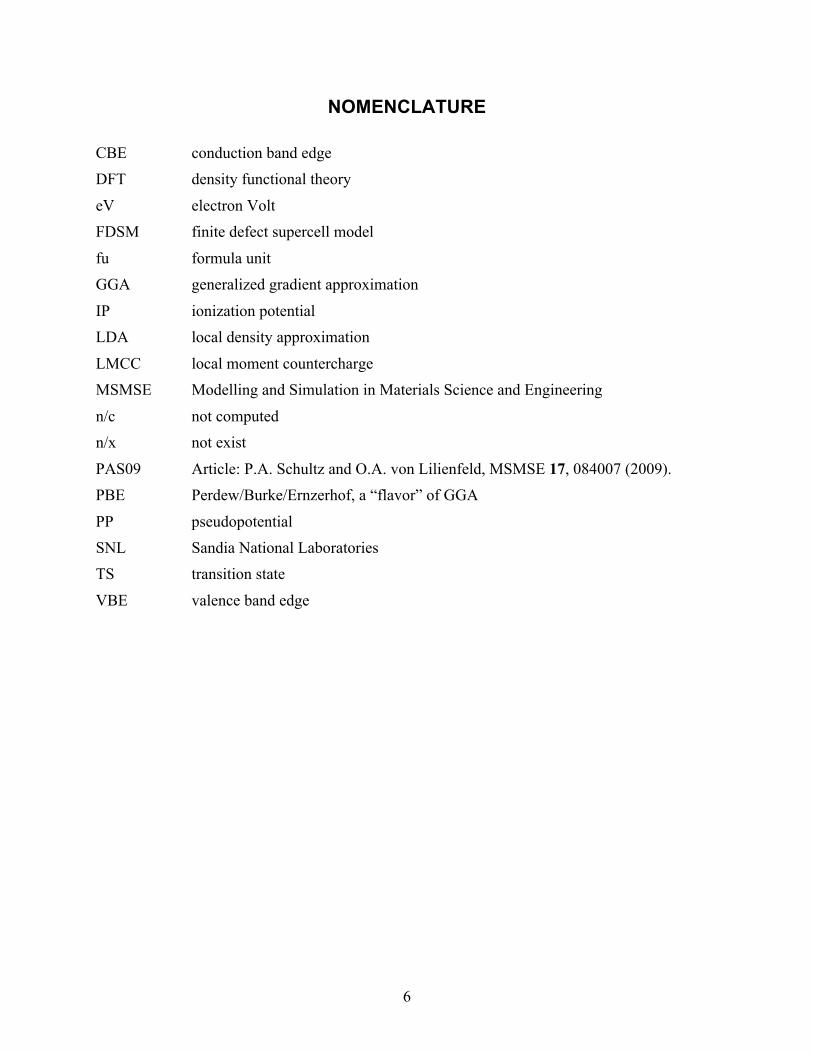
NOMENCLATURE
CBE conduction band edge DFT density functional theory
eV electron Volt FDSM finite defect supercell model
fu formula unit GGA generalized gradient approximation
IP ionization potential LDA local density approximation
LMCC local moment countercharge MSMSE Modelling and Simulation in Materials Science and Engineering
n/c not computed n/x not exist
PAS09 Article: P.A. Schultz and O.A. von Lilienfeld, MSMSE 17, 084007 (2009). PBE Perdew/Burke/Ernzerhof, a “flavor” of GGA
PP pseudopotential SNL Sandia National Laboratories TS transition state
VBE valence band edge
7
1. INTRODUCTION
The numerical results for density functional theory (DFT) calculations of properties of simple intrinsic defects in indium arsenide are presented. The results of the defect calculations are summarized in a series of numerical Tables containing the parameters needed to populate defect physics packages needed for device simulations. In addition, a summary of the InAs-specific verification and validation evidence is presented that provides a basis for estimating an overall uncertainty in predicted relative defect energy levels of the same size as for earlier simulations of silicon defects [1] and GaAs defects [2] (henceforth, “PAS09”), namely, 0.1-0.2 eV accuracy or uncertainty.
In indium arsenide, there is additionally a global uncertainty concerning the position of the valence band (VB) and conduction band (CB) edges with respect to the computed defect levels. Some of this can be attributed to limitations of the DFT methods, which do not predict band edges to the equivalent accuracy as defect charge transition energy levels. The larger part of this uncertainty stems from the very small band gap in InAs—small uncertainties in the band gap seem large in comparison—and, most, prominently, due to lack of any reliable experimental data for even one defect level to use as a marker. Following a long-term strategy for modeling III-V-materials with DFT methods, we use lessons learned from comprehensive defect studies in Si [1] and other III-V materials [3-6], with better data for calibration, to guide the choice of assumptions in defining the band edges for defect levels in InAs. As better information becomes available concerning the location of the band edges in the InAs defect level spectrum, the defect level in this Report could be straightforwardly shifted in order to make the defect level spectrum and the derived defect formation energies made consistent with the new band gap window.
1.1. Computational methods The details of the computational methods are comprehensive described previously in PAS09 (as applied to GaAs), and will only be briefly summarized here. The DFT calculations were performed with the SEQQUEST code [7]. The defect calculations were performed with semi-local functionals, using both the local density approximation (LDA) [8] and the Perdew-Burke-Ernzerhof (PBE) flavor of the generalized gradient approximation [9], this comparison being a partial assessment of the physical uncertainties within DFT functionals [10]. Both 3d-core and 3d-valence pseudopotentials (PP) for indium were used in defect calculations, to test (verify) the convergence in the PP construction for defect properties, the same as was done previously for defects in InP [5] using the same pseudopotentials for In.
The calculations of charged defects used the Finite Defect Supercell Model (FDSM) [1] to incorporate rigorous boundary conditions for the solution of the electrostatic potential in a charged supercell [11] and extrapolate all computed defect energies to the infinitely dilute limit. Defect calculations were performed using 64-atom, 216-atom, 512-atom, and 1000-atom cubic supercells. In convergence studies, 216-site supercell calculations proved sufficiently converged to achieve the required accuracy and are the basis for the production results listed in this Report. These simulation contexts are labeled in the following as: LDA64, LDA, LDA512, and LDA1000, for 64-site, 216-site, 512-site, and 1000-site, respectively, supercell calculations using LDA and the 3d-core (Z=3) PP for In; PBE for the 216-site supercells using PBE and 3d-core PP
8
for In atoms; and LDA-3d and PBE-3d for the 216-site supercells with 3d-valence (Z=13) PP for the In atoms.
1.2. Verification and validation The defect level calculations all use SEQQUEST and the FDSM, the same methods used in DFT calculations of defects in silicon and GaAs, which yielded mean absolute errors of 0.1 eV and maximum absolute error of 0.2 eV for defect levels over a wide sampling of different defects. This is the expected accuracy (uncertainties) of the methods for these defect level calculations in InAs, and the limit of the physical accuracy of the DFT approximations used in this analysis.
The arsenic PP has been described previously [12]: a standard s2p3 valence atom, added a d-potential with Rc=1.08 Bohr as the local potential. The indium PP was developed using the same systematic procedure used for the gallium PP for GaAs [12]. Both the 3d-core and 3d-valence PP were constructed using the generalized norm-conserving pseudopotential method of Hamann [13]. The 3d-core indium PP was extended to use a “hard” f-potential (Rf=1.1 Bohr) as the local potential and also added a partial core correction [14] to enhance transferability. The d-potential of the 3d-valence pseudopotential did not require a partial core correction, using the d-potential as the local potential achieves good transferability.
The In pseudopotentials correctly predict the experimental body-centered-tetragonal (bct) ground state structure of bulk In, preferng the bct over a fcc (face-centered-cubic) structure. For the As atom, the defect formation energy calculations use the optimum ground state A7 structure as the reference structure, the same as was done with the GaAs calculations in PAS09. As a test of transferability, LDA calculations with both In 3d-core and 3d-valence PP were performed for all defects. The differences between the 3d-core and 3d-valence results below are remarkably small, good evidence of the convergence of the In PP construction, verifying the In pseudopotentials. The largest difference in formation energies of neutral defects) is 0.13 eV (for the indium antisite, InAs), the largest difference in any defect formation energy is 0.23 (for the InAs(2-)), and the differences are typically much smaller. The largest difference between a computed defect level for the 3d-core and 3d-valence PP is 0.09 eV, for the vv(0/1-) transition, but that is an outlier: the average deviation between 3d-core ad 3d-valence defect energy levels is only ~0.02 eV and over half of the computed levels are within 0.01 eV, indicating an effective cancellation of errors is occurring in the defect level calculations. Hence, uncertainties in the absolute formation energies due to PP might be as large as 0.23 eV, but the (3d-core) defect levels, obtained as differences in formation energies, have much smaller uncertainties, much less than 0.1 eV, with respect to PP construction.
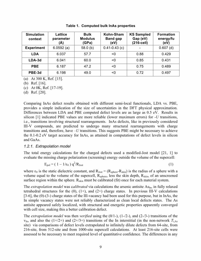
Bulk properties obtained for InAs in these different simulation contexts are presented in the Table 1. The lattice parameter and bulk modulus are well reproduced by both LDA and PBE, slightly better with LDA. Of particular note for InAs is that the Kohn-Sham gap vanishes for all contexts (functional and pseudopotentials), ostensibly precluding identification of localized levels within the band gap. The gap closes at the gamma point, however, and the standard k-point sampling for the cubic supercells avoids the gamma, and the discrete k-point sampling does have a sizeable gap, quoted in the Table for the sampling in the 216-site cells, within which clean localized defect states can be found. The heat of formation is the formation energy per InAs formula unit (fu) of InAs from elemental bulk In (bct structure) and As (A7 structure).
9
Table 1. Computed bulk InAs properties
Simulation context
Lattice parameter
(Å)
Bulk Modulus
(GPa)
Kohn-Sham Band gap
(eV)
KS Sampled Gap (eV) (216-cell)
Formation energy/fu
(eV) Experiment 6.0592 (a) 58.0 (b) 0.41-0.43 (c) - 0.607 (d)
LDA 6.037 57.7 <0 0.88 0.429
LDA-3d 6.041 60.0 <0 0.85 0.431
PBE 6.187 47.2 <0 0.75 0.489
PBE-3d 6.198 49.0 <0 0.72 0.497
(a) At 300 K, Ref. [15]. (b) Ref. [16]. (c) At 0K, Ref. [17-19]. (d) Ref. [20]. Comparing InAs defect results obtained with different semi-local functionals, LDA vs. PBE, provides a simple indication of the size of uncertainties in the DFT physical approximation. Differences between LDA and PBE computed defect levels are as large as 0.5 eV. Results in silicon [1] indicated PBE values are more reliable (lower maximum errors) for -U transitions, i.e., transitions involving structural rearrangements. InAs defects, like in previously considered III-V compounds, are predicted to undergo many structural rearrangements with charge transitions and, therefore, have –U transitions. This suggests PBE might be necessary to achieve the 0.1-0.2 eV target accuracy for InAs, as attained in computations of defect levels in silicon and GaAs.
1.2.1. Extrapolation model The total energy calculations for the charged defects used a modified-Jost model [21, 1] to evaluate the missing charge polarization (screening) energy outside the volume of the supercell:
Epol = ( 1 – 1/ε0 ) q2/RJost (1)
where ε0 is the static dielectric constant, and RJost = (Rsphere-Rskin) is the radius of a sphere with a volume equal to the volume of the supercell, Rsphere, less the skin depth, Rskin, of an unscreened surface region within the sphere. Rskin must be calibrated (fit) once for each material system.
The extrapolation model was calibrated via calculations the arsenic antisite AsIn, in fully relaxed tetrahedral structures for the (0), (1+), and (2+) charge states. In previous III-V calculations [3-6], the (0)-(3-) charge states of the III-vacancy had been used for this purpose, but in InAs, the In simple vacancy states were not reliably characterized as clean local defects states. The As antisite appeared safely localized, with structural and energetic properties apparently converged with cell size, making this a better calibration defect.
The extrapolation model was then verified using the (0/1-), (1-/2-), and (2-/3-) transitions of the vIn, and also the (1+/2+) and (2+/3+) transitions of the In interstitial (in the non-network Ti,As site) via comparisons of defect levels extrapolated to infinitely dilute defects from 64-site, from 216-site, from 512-site and from 1000-site supercell calculations. At least 216-site cells were assessed to be necessary to meet required level of quantitative confidence. The differences in any
10
defect level was typically smaller than 0.05 eV, indicating uncertainty with respect to cell size (and k-point sampling) is less than 0.05 eV, even for the extreme charge states.
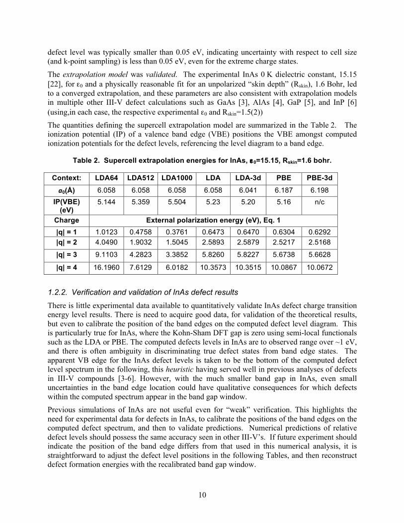
The extrapolation model was validated. The experimental InAs 0 K dielectric constant, 15.15 [22], for ε0 and a physically reasonable fit for an unpolarized “skin depth” (Rskin), 1.6 Bohr, led to a converged extrapolation, and these parameters are also consistent with extrapolation models in multiple other III-V defect calculations such as GaAs [3], AlAs [4], GaP [5], and InP [6] (using,in each case, the respective experimental ε0 and Rskin=1.5(2)) The quantities defining the supercell extrapolation model are summarized in the Table 2. The ionization potential (IP) of a valence band edge (VBE) positions the VBE amongst computed ionization potentials for the defect levels, referencing the level diagram to a band edge.
Table 2. Supercell extrapolation energies for InAs, ε0=15.15, Rskin=1.6 bohr.
Context: LDA64 LDA512 LDA1000 LDA LDA-3d PBE PBE-3d
a0(Å) 6.058 6.058 6.058 6.058 6.041 6.187 6.198 IP(VBE)
(eV) 5.144 5.359 5.504 5.23 5.20 5.16 n/c
Charge External polarization energy (eV), Eq. 1 |q| = 1 1.0123 0.4758 0.3761 0.6473 0.6470 0.6304 0.6292 |q| = 2 4.0490 1.9032 1.5045 2.5893 2.5879 2.5217 2.5168
|q| = 3 9.1103 4.2823 3.3852 5.8260 5.8227 5.6738 5.6628
|q| = 4 16.1960 7.6129 6.0182 10.3573 10.3515 10.0867 10.0672
1.2.2. Verification and validation of InAs defect results
There is little experimental data available to quantitatively validate InAs defect charge transition energy level results. There is need to acquire good data, for validation of the theoretical results, but even to calibrate the position of the band edges on the computed defect level diagram. This is particularly true for InAs, where the Kohn-Sham DFT gap is zero using semi-local functionals such as the LDA or PBE. The computed defects levels in InAs are to observed range over ~1 eV, and there is often ambiguity in discriminating true defect states from band edge states. The apparent VB edge for the InAs defect levels is taken to be the bottom of the computed defect level spectrum in the following, this heuristic having served well in previous analyses of defects in III-V compounds [3-6]. However, with the much smaller band gap in InAs, even small uncertainties in the band edge location could have qualitative consequences for which defects within the computed spectrum appear in the band gap window. Previous simulations of InAs are not useful even for “weak” verification. This highlights the need for experimental data for defects in InAs, to calibrate the positions of the band edges on the computed defect spectrum, and then to validate predictions. Numerical predictions of relative defect levels should possess the same accuracy seen in other III-V’s. If future experiment should indicate the position of the band edge differs from that used in this numerical analysis, it is straightforward to adjust the defect level positions in the following Tables, and then reconstruct defect formation energies with the recalibrated band gap window.
11
2. RESULTS
The section contains the Tables that summarize the numerical results for DFT simulations of defects in InAs.
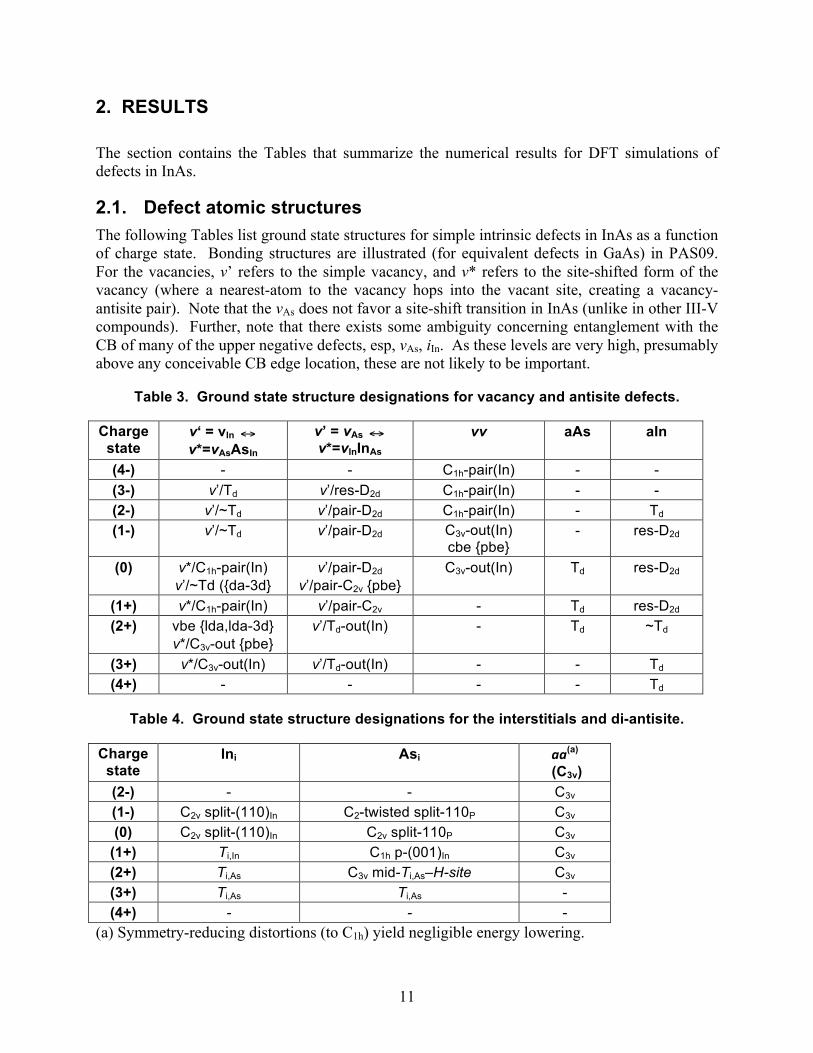
2.1. Defect atomic structures The following Tables list ground state structures for simple intrinsic defects in InAs as a function of charge state. Bonding structures are illustrated (for equivalent defects in GaAs) in PAS09. For the vacancies, v’ refers to the simple vacancy, and v* refers to the site-shifted form of the vacancy (where a nearest-atom to the vacancy hops into the vacant site, creating a vacancy-antisite pair). Note that the vAs does not favor a site-shift transition in InAs (unlike in other III-V compounds). Further, note that there exists some ambiguity concerning entanglement with the CB of many of the upper negative defects, esp, vAs, iIn. As these levels are very high, presumably above any conceivable CB edge location, these are not likely to be important.
Table 3. Ground state structure designations for vacancy and antisite defects.
Charge state
v‘ = vIn
€
↔ v*=vAsAsIn
v’ = vAs
€
↔ v*=vInInAs
vv aAs aIn
(4-) - - C1h-pair(In) - - (3-) v’/Td v’/res-D2d C1h-pair(In) - - (2-) v’/~Td v’/pair-D2d C1h-pair(In) - Td (1-) v’/~Td v’/pair-D2d C3v-out(In)
cbe {pbe} - res-D2d
(0) v*/C1h-pair(In) v’/~Td ({da-3d}
v’/pair-D2d
v’/pair-C2v {pbe} C3v-out(In) Td res-D2d
(1+) v*/C1h-pair(In) v’/pair-C2v - Td res-D2d (2+) vbe {lda,lda-3d}
v*/C3v-out {pbe} v’/Td-out(In) - Td ~Td
(3+) v*/C3v-out(In) v’/Td-out(In) - - Td (4+) - - - - Td
Table 4. Ground state structure designations for the interstitials and di-antisite.
Charge state
Ini Asi aa(a) (C3v)
(2-) - - C3v (1-) C2v split-(110)In C2-twisted split-110P C3v (0) C2v split-(110)In C2v split-110P C3v
(1+) Ti,In C1h p-(001)In C3v (2+) Ti,As C3v mid-Ti,As–H-site C3v (3+) Ti,As Ti,As - (4+) - - -
(a) Symmetry-reducing distortions (to C1h) yield negligible energy lowering.
12
2.2. Defect charge transition energy levels This section presents the defect charge transition levels of the simple intrinsic defects in InAs, in eV, along with neutral defect formation energies. The defect level calculations are the principal result of this Report, the later formation energies are all derived from these results. All the listed transitions are between states that appeared to be localized defect charge states in the calculations, although some of the more negative states exhibited some ambiguity concerning entanglement with the conduction band. Transitions outside the band gap are states unstable to carrier emission, but are included as the band gap window may be revised in the future.
Table 5. Defect levels for the indium vacancy, in eV, referenced to the VBE: vIn (v’)
€
↔ vAs-AsIn (v*)
VIn
Context
Neutral formation
energy
Defect levels (eV), cf. VBE
(3+/2+)
(2+/1+)
(1+/0)
(0/1-)
(1-/2-)
(2-/3-)
(3-/4-) Unrelaxed Td-v’ (for polarization calibration)
LDA64 3.58 - - - 0.34 0.61 0.91 n/x LDA 3.62 - - - 0.41 0.63 0.91 n/x
LDA512 3.69 - - - 0.39 0.60 0.84 n/x LDA1000 3.72 - - - 0.37 0.57 0.77 n/x
Relaxed Td-v’ (for polarization calibration) LDA64 3.04 - - - 0.15 0.28 0.41 n/x
LDA 2.79 - - - 0.29 0.40 0.52 n/x LDA512 2.81 - - - 0.28 0.38 0.49 n/x
LDA1000 2.84 - - - 0.28 0.36 0.46 n/x Relaxed thermodynamic levels
LDA 2.71 0.07 -0.05 0.67 0.35 0.40 0.52 n/x LDA-3d 2.71 0.05 -0.02 0.65 0.30 0.40 0.52 n/x
PBE 2.47 0.44 -0.11 0.71 0.53 0.38 0.50 n/x PBE-3d n/c n/c n/c n/c n/c n/c n/c -
Table 6. Defect levels for the arsenic vacancy, in eV, referenced to the VBE: vAs (v’)
€
↔ vIn-InAs (v*)
VAs
Context
Neutral formation
energy
Defect levels (eV), cf. VBE
(3+/2+)
(2+/1+)
(1+/0)
(0/1-)
(1-/2-)
(2-/3-)
(3-/4-) LDA 2.64 0.25 -0.33 0.63 0.39 1.14 0.93 n/x
LDA-3d 2.63 0.26 -0.33 0.62 0.39 1.11 0.92 n/x PBE 2.51 0.41 -0.15 0.69 0.52 1.09 0.95 n/x
PBE-3d n/c n/c n/c n/c n/c n/c n/c -
13
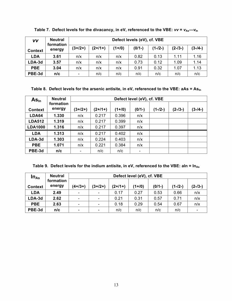
Table 7. Defect levels for the divacancy, in eV, referenced to the VBE: vv = vAs—vIn
vv
Context
Neutral formation
energy
Defect levels (eV), cf. VBE
(3+/2+) (2+/1+) (1+/0) (0/1-) (1-/2-) (2-/3-) (3-/4-)
LDA 3.61 n/x n/x n/x 0.82 0.13 1.11 1.16 LDA-3d 3.57 n/x n/x n/x 0.73 0.12 1.09 1.14
PBE 3.04 n/x n/x n/x 0.91 0.32 1.07 1.13 PBE-3d n/c - n/c n/c n/c n/c n/c n/c
Table 8. Defect levels for the arsenic antisite, in eV, referenced to the VBE: aAs = AsIn
AsIn
Context
Neutral formation
energy
Defect level (eV), cf. VBE
(3+/2+)
(2+/1+)
(1+/0)
(0/1-)
(1-/2-)
(2-/3-)
(3-/4-) LDA64 1.330 n/x 0.217 0.396 n/x
LDA512 1.319 n/x 0.217 0.399 n/x LDA1000 1.316 n/x 0.217 0.397 n/x
LDA 1.313 n/x 0.217 0.402 n/x LDA-3d 1.303 n/x 0.224 0.403 n/x
PBE 1.071 n/x 0.221 0.384 n/x PBE-3d n/c - n/c n/c -
Table 9. Defect levels for the indium antisite, in eV, referenced to the VBE: aIn = InAs
InAs
Context
Neutral formation
energy
Defect level (eV), cf. VBE
(4+/3+)
(3+/2+)
(2+/1+)
(1+/0)
(0/1-)
(1-/2-)
(2-/3-) LDA 2.49 - - 0.17 0.27 0.53 0.66 n/x
LDA-3d 2.62 - - 0.21 0.31 0.57 0.71 n/x PBE 2.63 - - 0.18 0.29 0.54 0.67 n/x
PBE-3d n/c - - n/c n/c n/c n/c -
14
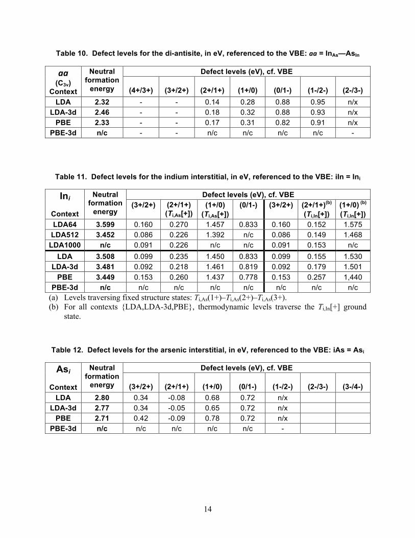
Table 10. Defect levels for the di-antisite, in eV, referenced to the VBE: aa = InAs—AsIn
aa (C3v)
Context
Neutral formation
energy
Defect levels (eV), cf. VBE
(4+/3+)
(3+/2+)
(2+/1+)
(1+/0)
(0/1-)
(1-/2-)
(2-/3-) LDA 2.32 - - 0.14 0.28 0.88 0.95 n/x
LDA-3d 2.46 - - 0.18 0.32 0.88 0.93 n/x PBE 2.33 - - 0.17 0.31 0.82 0.91 n/x
PBE-3d n/c - - n/c n/c n/c n/c -
Table 11. Defect levels for the indium interstitial, in eV, referenced to the VBE: iIn = Ini
Ini
Context
Neutral formation
energy
Defect levels (eV), cf. VBE (3+/2+) (2+/1+)
(Ti,As[+]) (1+/0)
(Ti,As[+]) (0/1-) (3+/2+) (2+/1+)(b)
(Ti,In[+]) (1+/0) (b) (Ti,In[+])
LDA64 3.599 0.160 0.270 1.457 0.833 0.160 0.152 1.575 LDA512 3.452 0.086 0.226 1.392 n/c 0.086 0.149 1.468
LDA1000 n/c 0.091 0.226 n/c n/c 0.091 0.153 n/c LDA 3.508 0.099 0.235 1.450 0.833 0.099 0.155 1.530
LDA-3d 3.481 0.092 0.218 1.461 0.819 0.092 0.179 1.501 PBE 3.449 0.153 0.260 1.437 0.778 0.153 0.257 1,440
PBE-3d n/c n/c n/c n/c n/c n/c n/c n/c (a) Levels traversing fixed structure states: Ti,As(1+)–Ti,As(2+)–Ti,As(3+). (b) For all contexts {LDA,LDA-3d,PBE}, thermodynamic levels traverse the Ti,In[+] ground
state.
Table 12. Defect levels for the arsenic interstitial, in eV, referenced to the VBE: iAs = Asi
Asi
Context
Neutral formation
energy
Defect levels (eV), cf. VBE
(3+/2+)
(2+/1+)
(1+/0)
(0/1-)
(1-/2-)
(2-/3-)
(3-/4-) LDA 2.80 0.34 -0.08 0.68 0.72 n/x
LDA-3d 2.77 0.34 -0.05 0.65 0.72 n/x PBE 2.71 0.42 -0.09 0.78 0.72 n/x
PBE-3d n/c n/c n/c n/c n/c -
15
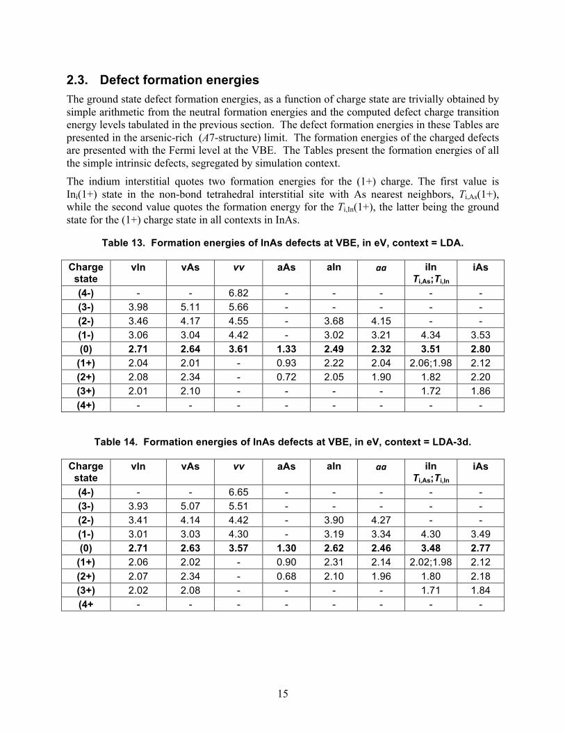
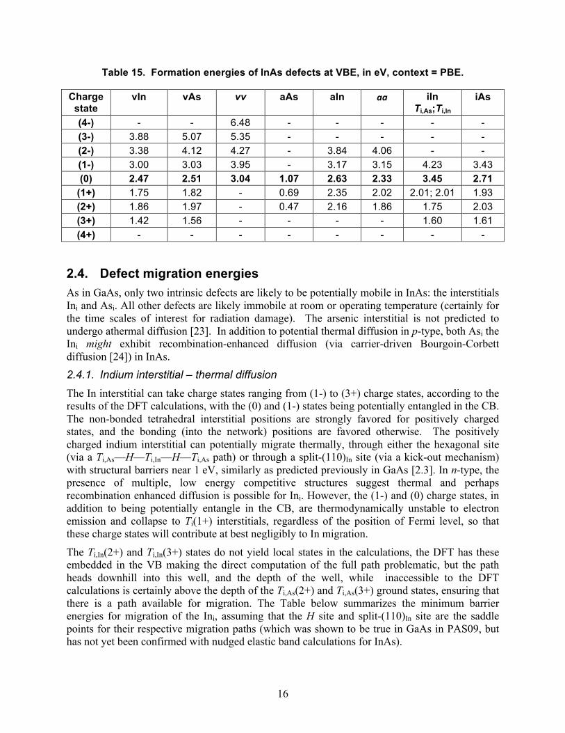
2.3. Defect formation energies The ground state defect formation energies, as a function of charge state are trivially obtained by simple arithmetic from the neutral formation energies and the computed defect charge transition energy levels tabulated in the previous section. The defect formation energies in these Tables are presented in the arsenic-rich (A7-structure) limit. The formation energies of the charged defects are presented with the Fermi level at the VBE. The Tables present the formation energies of all the simple intrinsic defects, segregated by simulation context. The indium interstitial quotes two formation energies for the (1+) charge. The first value is Ini(1+) state in the non-bond tetrahedral interstitial site with As nearest neighbors, Ti,As(1+), while the second value quotes the formation energy for the Ti,In(1+), the latter being the ground state for the (1+) charge state in all contexts in InAs.
Table 13. Formation energies of InAs defects at VBE, in eV, context = LDA.
Charge state
vIn vAs vv aAs aIn
aa iIn Ti,As;Ti,In
iAs
(4-) - - 6.82 - - - - - (3-) 3.98 5.11 5.66 - - - - - (2-) 3.46 4.17 4.55 - 3.68 4.15 - - (1-) 3.06 3.04 4.42 - 3.02 3.21 4.34 3.53 (0) 2.71 2.64 3.61 1.33 2.49 2.32 3.51 2.80
(1+) 2.04 2.01 - 0.93 2.22 2.04 2.06;1.98 2.12 (2+) 2.08 2.34 - 0.72 2.05 1.90 1.82 2.20 (3+) 2.01 2.10 - - - - 1.72 1.86 (4+) - - - - - - - -
Table 14. Formation energies of InAs defects at VBE, in eV, context = LDA-3d.
Charge state
vIn vAs vv aAs aIn
aa iIn Ti,As;Ti,In
iAs
(4-) - - 6.65 - - - - - (3-) 3.93 5.07 5.51 - - - - - (2-) 3.41 4.14 4.42 - 3.90 4.27 - - (1-) 3.01 3.03 4.30 - 3.19 3.34 4.30 3.49 (0) 2.71 2.63 3.57 1.30 2.62 2.46 3.48 2.77
(1+) 2.06 2.02 - 0.90 2.31 2.14 2.02;1.98 2.12 (2+) 2.07 2.34 - 0.68 2.10 1.96 1.80 2.18 (3+) 2.02 2.08 - - - - 1.71 1.84 (4+ - - - - - - - -
16
Table 15. Formation energies of InAs defects at VBE, in eV, context = PBE.
Charge state
vIn vAs vv aAs aIn aa iIn Ti,As;Ti,In
iAs
(4-) - - 6.48 - - - - - (3-) 3.88 5.07 5.35 - - - - - (2-) 3.38 4.12 4.27 - 3.84 4.06 - - (1-) 3.00 3.03 3.95 - 3.17 3.15 4.23 3.43 (0) 2.47 2.51 3.04 1.07 2.63 2.33 3.45 2.71
(1+) 1.75 1.82 - 0.69 2.35 2.02 2.01; 2.01 1.93 (2+) 1.86 1.97 - 0.47 2.16 1.86 1.75 2.03 (3+) 1.42 1.56 - - - - 1.60 1.61 (4+) - - - - - - - -
2.4. Defect migration energies As in GaAs, only two intrinsic defects are likely to be potentially mobile in InAs: the interstitials Ini and Asi. All other defects are likely immobile at room or operating temperature (certainly for the time scales of interest for radiation damage). The arsenic interstitial is not predicted to undergo athermal diffusion [23]. In addition to potential thermal diffusion in p-type, both Asi the Ini might exhibit recombination-enhanced diffusion (via carrier-driven Bourgoin-Corbett diffusion [24]) in InAs. 2.4.1. Indium interstitial – thermal diffusion
The In interstitial can take charge states ranging from (1-) to (3+) charge states, according to the results of the DFT calculations, with the (0) and (1-) states being potentially entangled in the CB. The non-bonded tetrahedral interstitial positions are strongly favored for positively charged states, and the bonding (into the network) positions are favored otherwise. The positively charged indium interstitial can potentially migrate thermally, through either the hexagonal site (via a Ti,As—H—Ti,In—H—Ti,As path) or through a split-(110)In site (via a kick-out mechanism) with structural barriers near 1 eV, similarly as predicted previously in GaAs [2.3]. In n-type, the presence of multiple, low energy competitive structures suggest thermal and perhaps recombination enhanced diffusion is possible for Ini. However, the (1-) and (0) charge states, in addition to being potentially entangle in the CB, are thermodynamically unstable to electron emission and collapse to Ti(1+) interstitials, regardless of the position of Fermi level, so that these charge states will contribute at best negligibly to In migration.
The Ti,In(2+) and Ti,In(3+) states do not yield local states in the calculations, the DFT has these embedded in the VB making the direct computation of the full path problematic, but the path heads downhill into this well, and the depth of the well, while inaccessible to the DFT calculations is certainly above the depth of the Ti,As(2+) and Ti,As(3+) ground states, ensuring that there is a path available for migration. The Table below summarizes the minimum barrier energies for migration of the Ini, assuming that the H site and split-(110)In site are the saddle points for their respective migration paths (which was shown to be true in GaAs in PAS09, but has not yet been confirmed with nudged elastic band calculations for InAs).
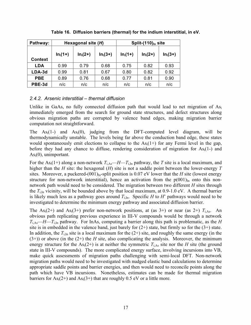
17
Table 16. Diffusion barriers (thermal) for the indium interstitial, in eV.
Pathway: Hexagonal site (H) Split-(110)In site
Context
Ini(1+)
Ini(2+)
Ini(3+)
Ini(1+)
Ini(2+)
Ini(3+)
LDA 0.99 0.79 0.68 0.75 0.82 0.93 LDA-3d 0.99 0.81 0.67 0.80 0.82 0.92
PBE 0.89 0.76 0.68 0.77 0.81 0.90 PBE-3d n/c n/c n/c n/c n/c n/c
2.4.2. Arsenic interstitial – thermal diffusion
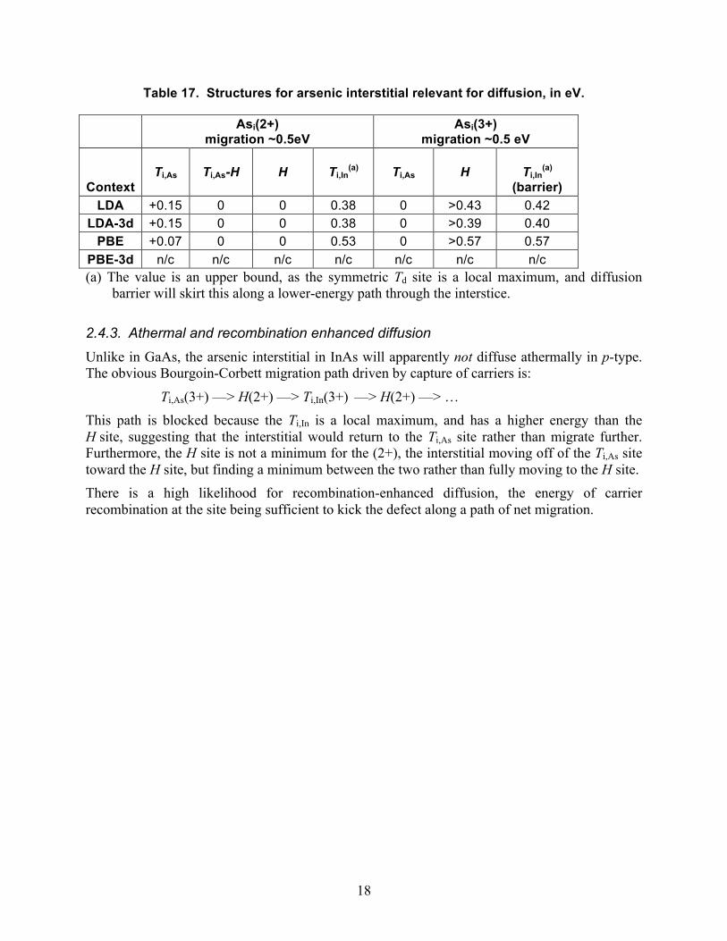
Unlike in GaAs, no fully connected diffusion path that would lead to net migration of Asi immediately emerged from the search for ground state structures, and defect structures along obvious migration paths are corrupted by valence band edges, making migration barrier computation not straightforward.
The Asi(1-) and Asi(0), judging from the DFT-computed level diagram, will be thermodynamically unstable. The levels being far above the conduction band edge, these states would spontaneously emit elections to collapse to the Asi(1+) for any Fermi level in the gap, before they had any chance to diffuse, rendering consideration of migration for Asi(1-) and Asi(0), unimportant. For the Asi(1+) along a non-network Ti,As—H—Ti,In pathway, the T site is a local maximum, and higher than the H site: the hexagonal (H) site is not a saddle point between the lower-energy T sites. Moreover, a puckered-(001)In-split position is 0.07 eV lower that the H site (lowest energy structure for non-network interstitial), hence an activation from the p(001)In onto this non-network path would need to be considered. The migration between two different H sites through the Ti,In vicinity, will be bounded above by that local maximum, at 0.9-1.0 eV. A thermal barrier is likely much less as a pathway goes around Ti,In. Specific H to H’ pathways would need to be investigated to determine the minimum energy pathway and associated diffusion barrier. The Asi(2+) and Asi(3+) prefer non-network positions, at (as 3+) or near (as 2+) Ti,As. An obvious path replicating previous experience in III-V compounds would be through a network Ti,As—H—Ti,In pathway. For InAs, computing a barrier along this path is problematic, as the H site is in embedded in the valence band, just barely for (2+) state, but firmly so for the (3+) state. In addition, the Ti,In site is a local maximum for the (2+) site, and roughly the same energy (in the (3+)) or above (in the (2+) the H site, also complicating the analysis. Moreover, the minimum energy structure for the Asi(2+) is at neither the symmetric Ti,As site nor the H site (the ground state in III-V compounds). The more complicated energy surface, involving incursions into VB, make quick assessments of migration paths challenging with semi-local DFT. Non-network migration paths would need to be investigated with nudged elastic band calculations to determine appropriate saddle points and barrier energies, and then would need to reconcile points along the path which have VB incursions. Nonetheless, estimates can be made for thermal migration barriers for Asi(2+) and Asi(3+) that are roughly 0.5 eV or a little more.
18
Table 17. Structures for arsenic interstitial relevant for diffusion, in eV.
Asi(2+) migration ~0.5eV
Asi(3+) migration ~0.5 eV
Context
Ti,As
Ti,As-H
H
Ti,In
(a)
Ti,As
H
Ti,In
(a) (barrier)
LDA +0.15 0 0 0.38 0 >0.43 0.42 LDA-3d +0.15 0 0 0.38 0 >0.39 0.40
PBE +0.07 0 0 0.53 0 >0.57 0.57 PBE-3d n/c n/c n/c n/c n/c n/c n/c (a) The value is an upper bound, as the symmetric Td site is a local maximum, and diffusion
barrier will skirt this along a lower-energy path through the interstice. 2.4.3. Athermal and recombination enhanced diffusion
Unlike in GaAs, the arsenic interstitial in InAs will apparently not diffuse athermally in p-type. The obvious Bourgoin-Corbett migration path driven by capture of carriers is:
Ti,As(3+) —> H(2+) —> Ti,In(3+) —> H(2+) —> … This path is blocked because the Ti,In is a local maximum, and has a higher energy than the H site, suggesting that the interstitial would return to the Ti,As site rather than migrate further. Furthermore, the H site is not a minimum for the (2+), the interstitial moving off of the Ti,As site toward the H site, but finding a minimum between the two rather than fully moving to the H site. There is a high likelihood for recombination-enhanced diffusion, the energy of carrier recombination at the site being sufficient to kick the defect along a path of net migration.
19
3. CONCLUSIONS
The parameters needed to describe the defect properties of simple intrinsic defects in InAs are summarized into Tables. The small band gap, lack of a definitive marker to locate a band edge for the defect spectrum, and frequent ambiguity of contamination of defects states make the analysis much more uncertain than defect calculations for previous III-V compounds. Reliable experimental studies to calibrate these results are needed, and investigations with density functional containing explicit exchange might be advisable.
4. REFERENCES
1. P.A. Schultz, Phys. Rev. Lett. 96, 246401 (2006).
2. P.A. Schultz and O.A. von Lilienfeld, Modelling Simul. Mater. Sci. Eng. 17, 084007 (2009).
3. P.A. Schultz, “Simple intrinsic defects in GaAs: Numerical Supplement”, SAND2012-2675, Sandia National Laboratories, Albuquerque, NM, April 2012. [Unclassified]
4. P.A. Schultz, “First principles predictions of intrinsic defects in aluminum atrsenide, AlAs: Numerical supplement”, SAND2012-2938, Sandia National Laboratories, Albuquerque, NM, April 2012. [Unclassified]
5. P.A. Schultz, “Simple intrinsic defects in InP: Numerical predictions”, SAND2012-3313, Sandia National Laboratories, Albuquerque, NM, April 2012. [Unclassified]
6. P.A. Schultz, “Simple intrinsic defects in GaP: Numerical predictions”, SAND2012-3314, Sandia National Laboratories, Albuquerque, NM, April 2012. [Unclassified]
7. P.A. Schultz, SEQQUEST code, unpublished, see http://dft.sandia.gov/quest/
8. J.P. Perdew and A. Zunger, Phys. Rev. 23, 5048 (1981). 9. J.P. Perdew, K. Burke, and M. Ernzerhof, Phys. Rev. Lett. 77, 3865 (1996).
10. A.E. Mattsson, P.A. Schultz, M.P. Desjarlais, T.R. Mattsson, and K. Leung, Modelling Simul. Mater. Sci. Eng. 13, R1 (2005).
11. P.A. Schultz, Phys. Rev. Lett. 84, 1942 (2000). 12. O.A. von Lilienfeld and P.A. Schultz, Phys. Rev. B 77, 115202 (2008).
13. D.R. Hamann, Phys. Rev. B 40, 2980 (1989). 14. S.G. Louie, S. Froyen, and M.L. Cohen, Phys. Rev. B 26, 1738 (1982).
15. R.E. Nahory, M.A. Pollack, W.D. Johnston, and R.L. Burns, Appl. Phys. Lett. 33, 659 (1978).
16. D. Gerlich, J. Appl. Phys. 34, 2915 (1963).
20
17. Y.P. Varshni, Physica 34, 149 (1967), in an analysis based on date from J.R. Dixon and J.M. Ellis, Phys. Rev. 123, 1560 (1961).
18. Z.M. Fang, K.Y. Ma, D.H. Jaw, R.M. Cohen, and G.B. Stringfellow, J. Appl. Phys. 67, 7034 (1990).
19. Y. Lacroix, C.A. Tran, S.P. Watkins, and M.L.W. Thewalt, J. Appl. Phys. 80, 6416 (1996).
20. R. Lide (ed.), Handbook of Chemistry and Physics, 72nd Ed. (Boca Rotan: CRC Press, 1991).
21. W. Jost, J. Chem. Phys. 1, 466 (1933). 22. M. Hass and B.W. Henvis, J. Phys. Chem. Solids 23, 1099 (1962).
23. G.D. Watkins, in Radiation Damage in Semiconductors, ed. P. Baruch, p97 (Paris:Dunod, 1965).
24. J.C. Bourgoin and J.W. Corbett, Phys. Lett. A 38, 135 (1972).

21
This page intentionally left blank
22
DISTRIBUTION
(to be distributed electronically) 1 MS0899 Technical Library 9536 (electronic copy)