Embed Size (px)
Citation preview
PROJECT #1 SINE-∆ PWM INVERTER
JIN-WOO JUNG, PH.D STUDENT E-mail: [email protected]
Tel.: (614) 292-3633
ADVISOR: PROF. ALI KEYHANI
DATE: FEBRUARY 20, 2005
MECHATRONIC SYSTEMS LABORATORY
DEPARTMENT OF ELECTRICAL AND COMPUTER ENGINEERING
THE OHIO STATE UNIVERSITY

2
1. Problem Description
In this simulation, we will study Sine-∆ Pulse Width Modulation (PWM) technique. We will
use the SEMIKRON® IGBT Flexible Power Converter for this purpose. The system
configuration is given below:
Fig. 1 Circuit model of three-phase PWM inverter with a center-taped grounded DC bus.
The system parameters for this converter are as follows:
IGBTs: SEMIKRON SKM 50 GB 123D, Max ratings: VCES = 600 V, IC = 80 A
DC- link voltage: Vdc = 400 V
Fundamental frequency: f = 60 Hz
PWM (carrier) frequency: fz = 3 kHz
Modulation index: m = 0.8
Output filter: Lf = 800 µH and Cf = 400 µF
Load: Lload = 2 mH and Rload = 5 Ω
Using Matlab/Simulink, simulate the circuit model described in Fig. 1 and plot the
waveforms of Vi (= [ViAB ViBC ViCA]), Ii (= [iiA iiB iiC]), VL (= [VLAB VLBC VLCA]), and IL (= [iLA
iLB iLC]).
3
2. Sine-∆ PWM
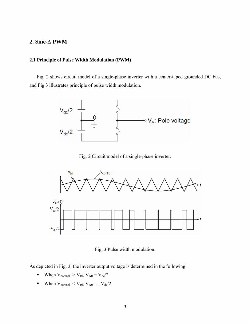
2.1 Principle of Pulse Width Modulation (PWM)
Fig. 2 shows circuit model of a single-phase inverter with a center-taped grounded DC bus,
and Fig 3 illustrates principle of pulse width modulation.
Fig. 2 Circuit model of a single-phase inverter.
Fig. 3 Pulse width modulation.
As depicted in Fig. 3, the inverter output voltage is determined in the following:
When Vcontrol > Vtri, VA0 = Vdc/2
When Vcontrol < Vtri, VA0 = −Vdc/2

4
Also, the inverter output voltage has the following features:
PWM frequency is the same as the frequency of Vtri
Amplitude is controlled by the peak value of Vcontrol
Fundamental frequency is controlled by the frequency of Vcontrol
Modulation index (m) is defined as:
A01A0
10
Vofcomponentfrequecnylfundamenta:)(Vwhere,
,2/
)(
dc
A
tri
control
VVofpeak
vv
m ==∴
2.2 Three-Phase Sine-∆ PWM Inverter
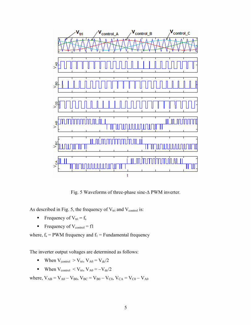
Fig. 4 shows circuit model of three-phase PWM inverter and Fig. 5 shows waveforms of
carrier wave signal (Vtri) and control signal (Vcontrol), inverter output line to neutral voltage (VA0,
VB0, VC0), inverter output line to line voltages (VAB, VBC, VCA), respectively.
Fig. 4 Three-phase PWM Inverter.
5
Fig. 5 Waveforms of three-phase sine-∆ PWM inverter.
As described in Fig. 5, the frequency of Vtri and Vcontrol is:
Frequency of Vtri = fs
Frequency of Vcontrol = f1
where, fs = PWM frequency and f1 = Fundamental frequency
The inverter output voltages are determined as follows:
When Vcontrol > Vtri, VA0 = Vdc/2
When Vcontrol < Vtri, VA0 = −Vdc/2
where, VAB = VA0 – VB0, VBC = VB0 – VC0, VCA = VC0 – VA0
6
3. State-Space Model
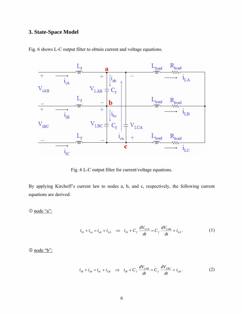
Fig. 6 shows L-C output filter to obtain current and voltage equations.
Fig. 6 L-C output filter for current/voltage equations.
By applying Kirchoff’s current law to nodes a, b, and c, respectively, the following current
equations are derived:
node “a”:
LALAB
fLCA
fiALAabcaiA idt
dVC
dtdV
Ciiiii +=+⇒+=+ . (1)
node “b”:
LBLBC
fLAB
fiBLBbcabiB idt
dVC
dtdV
Ciiiii +=+⇒+=+ . (2)

7
node “c”:
LCLCA
fLBC
fiCLCcabciC idt
dVC
dtdV
Ciiiii +=+⇒+=+ . (3)
where, .,,dt
dVCi
dtdV
Cidt
dVCi LCAfca
LBCfbc
LABfab ===
Also, (1) to (3) can be rewritten as the following equations, respectively:
subtracting (2) from (1):
LBLAiBiALABLBCLCA
f
LBLALBCLAB
fLABLCA
fiBiA
iiiidt
dVdt
dVdt
dVC
iidt
dVdt
dVC
dtdV
dtdV
Cii
−++−=⎟⎠
⎞⎜⎝
⎛ ⋅−+⇒
−+⎟⎠
⎞⎜⎝
⎛ −=⎟⎠
⎞⎜⎝
⎛ −+−
2
. (4)
subtracting (3) from (2):
LCLBiCiBLBCLCALAB
f
LCLBLCALBC
fLBCLAB
fiCiB
iiiidt
dVdt
dVdt
dVC
iidt
dVdt
dVC
dtdV
dtdV
Cii
−++−=⎟⎠
⎞⎜⎝
⎛ ⋅−+⇒
−+⎟⎠
⎞⎜⎝
⎛ −=⎟⎠
⎞⎜⎝
⎛ −+−
2
. (5)
subtracting (1) from (3):
LALCiAiCLCALBCLAB
f
LALCLABLCA
fLCALBC
fiAiC
iiiidt
dVdt
dVdt
dVC
iidt
dVdt
dVC
dtdV
dtdV
Cii
−++−=⎟⎠
⎞⎜⎝
⎛ ⋅−+⇒
−+⎟⎠
⎞⎜⎝
⎛ −=⎟⎠
⎞⎜⎝
⎛ −+−
2
. (6)
To simplify (4) to (6), we use the following relationship that an algebraic sum of line to line load
voltages is equal to zero:

8
VLAB + VLBC + VLCA = 0. (7)
Based on (7), the (4) to (6) can be modified to a first-order differential equation, respectively:
( )
( )
( )⎪⎪⎪
⎩
⎪⎪⎪
⎨
⎧
−=
−=
−=
LCAf
iCAf
LCA
CLBf
iBCf
LBC
LABf
iABf
LAB
iC
iCdt
dV
iC
iCdt
dV
iC
iCdt
dV
31
31
31
31
31
31
, (8)
where, iiAB = iiA iiB, iiBC = iiB iiC, iiCA
= iiC iiA and iLAB = iLA iLB, iLBC = iLB iLC,
iLCA = iLC iLA.
By applying Kirchoff’s voltage law on the side of inverter output, the following voltage
equations can be derived:
⎪⎪⎪
⎩
⎪⎪⎪
⎨
⎧
+−=
+−=
+−=
iCAf
LCAf
iCA
iBCf
LBCf
iBC
iABf
LABf
iAB
VL
VLdt
di
VL
VLdt
di
VL
VLdt
di
11
11
11
. (9)
By applying Kirchoff’s voltage law on the load side, the following voltage equations can be
derived:
⎪⎪⎪
⎩
⎪⎪⎪
⎨
⎧
−−+=
−−+=
−−+=
LAloadLA
loadLCloadLC
loadLCA
LCloadLC
loadLBloadLB
loadLBC
LBloadLB
loadLAloadLA
loadLAB
iRdt
diLiR
dtdi
LV
iRdt
diLiR
dtdi
LV
iRdt
diLiR
dtdi
LV
. (10)
9
Equation (10) can be rewritten as:
⎪⎪⎪⎪
⎩
⎪⎪⎪⎪
⎨
⎧
+−=
+−=
+−=
LCAload
LCAload
loadLCA
LBCload
LBCload
loadLBC
LABload
LABload
loadLAB
VL
iLR
dtdi
VL
iLR
dtdi
VL
iLR
dtdi
1
1
1
. (11)
Therefore, we can rewrite (8), (9) and (11) into a matrix form, respectively:
Lload
loadL
load
L
if
Lf
i
Lf
if
L
LR
Ldtd
LLdtd
CCdtd
IVI
VVI
IIV
−=
+−=
−=
1
11
31
31
, (12)
where, VL = [VLAB VLBC VLCA]T , Ii = [iiAB iiBC iiCA]T = [iiA-iiB iiB-iiC iiC-iiA]T , Vi = [ViAB ViBC ViCA]T ,
IL = = [iLAB iLBC iLCA]T = [iLA-iLB iLB-iLC iLC-iLA]T.
Finally, the given plant model (12) can be expressed as the following continuous-time state space
equation
)()()( ttt BuAXX +=& , (13)
where,
19×⎥⎥⎥
⎦
⎤
⎢⎢⎢
⎣
⎡=
L
i
L
IIV
X ,
99333333
333333
333333
01
0013
13
10
××××
×××
×××
⎥⎥⎥⎥⎥⎥⎥
⎦
⎤
⎢⎢⎢⎢⎢⎢⎢
⎣
⎡
−
−
−
=
ILR
IL
IL
IC
IC
load
load
load
f
ff
A ,
3933
33
33
0
10
××
×
×
⎥⎥⎥⎥
⎦
⎤
⎢⎢⎢⎢
⎣
⎡
= IL f
B , [ ] 13×= iVu .

10
Note that load line to line voltage VL, inverter output current Ii, and the load current IL are the
state variables of the system, and the inverter output line-to-line voltage Vi is the control input
(u).
4. Simulation Steps
1). Initialize system parameters using Matlab
2). Build Simulink Model
Generate carrier wave (Vtri) and control signal (Vcontrol) based on modulation index (m)
Compare Vtri to Vcontrol to get ViAn, ViBn, ViCn.
Generate the inverter output voltages (ViAB, ViBC, ViCA,) for control input (u)
Build state-space model
Send data to Workspace
3). Plot simulation results using Matlab

11
5. Simulation results
0.9 0.902 0.904 0.906 0.908 0.91 0.912 0.914 0.916 0.918 0.92
-1
0
1
Vtri
, Vsi
n [V
]
Vtri and Vsin and ViAn
VtriVsin
0.9 0.902 0.904 0.906 0.908 0.91 0.912 0.914 0.916 0.918 0.92-500
0
500
ViA
n [V
]
0.9 0.901 0.902 0.903 0.904 0.905 0.906 0.907 0.908 0.909
-1
0
1
Vtri
, Vsi
n [V
] VtriVsin
0.9 0.901 0.902 0.903 0.904 0.905 0.906 0.907 0.908 0.909-500
0
500
ViA
n [V
]
Time [Sec]
Fig. 7 Waveforms of carrier wave, control signal, and inverter output line to neutral voltage.
(a) Carrier wave (Vtri) and control signal (Vsin)
(b) Inverter output line to neutral voltage (ViAn)
(c) Enlarged carrier wave (Vtri) and control signal (Vsin)
(d) Enlarged inverter output line to neutral voltage (ViAn)

12
0.9 0.91 0.92 0.93 0.94 0.95 0.96 0.97 0.98 0.99 1-500
0
500V
iAB
[V]
Inverter output line to line voltages (ViAB, ViBC, ViCA)
0.9 0.91 0.92 0.93 0.94 0.95 0.96 0.97 0.98 0.99 1-500
0
500
ViB
C [V
]
0.9 0.91 0.92 0.93 0.94 0.95 0.96 0.97 0.98 0.99 1-500
0
500
ViC
A [V
]
Time [Sec]
Fig. 8 Simulation results of inverter output line to line voltages (ViAB, ViBC, ViCA)
13
0.9 0.91 0.92 0.93 0.94 0.95 0.96 0.97 0.98 0.99 1-100
-50
0
50
100i iA
[A]
Inverter output currents (iiA, iiB, iiC)
0.9 0.91 0.92 0.93 0.94 0.95 0.96 0.97 0.98 0.99 1-100
-50
0
50
100
i iB [A
]
0.9 0.91 0.92 0.93 0.94 0.95 0.96 0.97 0.98 0.99 1-100
-50
0
50
100
i iC [A
]
Time [Sec]
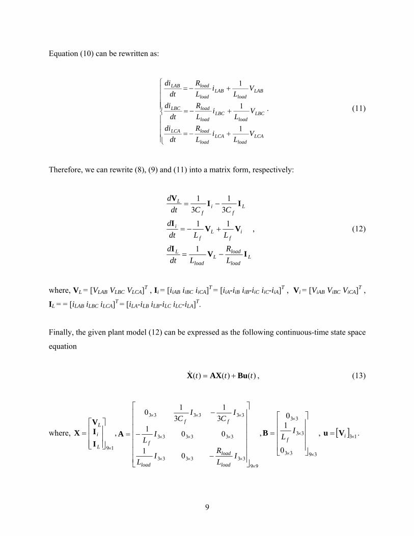
Fig. 9 Simulation results of inverter output currents (iiA, iiB, iiC)

14
0.9 0.91 0.92 0.93 0.94 0.95 0.96 0.97 0.98 0.99 1-400
-200
0
200
400V
LAB
[V]
Load line to line voltages (VLAB, VLBC, VLCA)
0.9 0.91 0.92 0.93 0.94 0.95 0.96 0.97 0.98 0.99 1-400
-200
0
200
400
VLB
C [V
]
0.9 0.91 0.92 0.93 0.94 0.95 0.96 0.97 0.98 0.99 1-400
-200
0
200
400
VLC
A [V
]
Time [Sec]
Fig. 10 Simulation results of load line to line voltages (VLAB, VLBC, VLCA)
15
0.9 0.91 0.92 0.93 0.94 0.95 0.96 0.97 0.98 0.99 1-50
0
50i LA
[A]
Load phase currents (iLA, iLB, iLC)
0.9 0.91 0.92 0.93 0.94 0.95 0.96 0.97 0.98 0.99 1-50
0
50
i LB [A
]
0.9 0.91 0.92 0.93 0.94 0.95 0.96 0.97 0.98 0.99 1-50
0
50
i LC [A
]
Time [Sec]
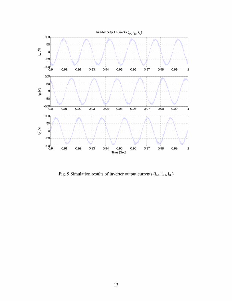
Fig. 11 Simulation results of load phase currents (iLA, iLB, iLC)

16
0.9 0.91 0.92 0.93 0.94 0.95 0.96 0.97 0.98 0.99 1-500
0
500V
iAB
[V]
0.9 0.91 0.92 0.93 0.94 0.95 0.96 0.97 0.98 0.99 1-100
0
100
i iA, i
iB, i
iC [A
] iiAiiBiiC
0.9 0.91 0.92 0.93 0.94 0.95 0.96 0.97 0.98 0.99 1-400
-200
0
200
400
VLA
B, V
LBC,
VLC
A [V
]
VLABVLBCVLCA
0.9 0.91 0.92 0.93 0.94 0.95 0.96 0.97 0.98 0.99 1-50
0
50
i LA, i
LB, i
LC [A
]
Time [Sec]
iLAiLBiLC
Fig. 12 Simulation waveforms.
(a) Inverter output line to line voltage (ViAB)
(b) Inverter output current (iiA)
(c) Load line to line voltage (VLAB)
(d) Load phase current (iLA)

17
Appendix
Matlab/Simulink Codes

18
A.1 Matlab Code for System Parameters
% Written by Jin Woo Jung, Date: 02/20/05
% ECE743, Simulation Project #1 (Sine PWM Inverter)
% Matlab program for Parameter Initialization
clear all % clear workspace
% Input data
Vdc= 400; % DC-link voltage
Lf= 800e-6;% Inductance for output filter
Cf= 400e-6; % Capacitance for output filter
Lload = 2e-3; %Load inductance
Rload= 5; % Load resistance
f= 60; % Fundamental frequency
fz = 3e3; % Switching frequency
m= 0.8; % Modulation index
% Coefficients for State-Space Model
A=[zeros(3,3) eye(3)/(3*Cf) -eye(3)/(3*Cf)
-eye(3)/Lf zeros(3,3) zeros(3,3)
eye(3,3)/Lload zeros(3,3) -eye(3)*Rload/Lload]; % system matrix
B=[zeros(3,3)
eye(3)/Lf
zeros(3,3)]; % coefficient for the control variable u
C=[eye(9)]; % coefficient for the output y
D=[zeros(9,3)]; % coefficient for the output y
Ks = 1/3*[-1 0 1; 1 -1 0; 0 1 -1]; % Conversion matrix to transform [iiAB iiBC iiCA] to [iiA iiB
iiC]
19
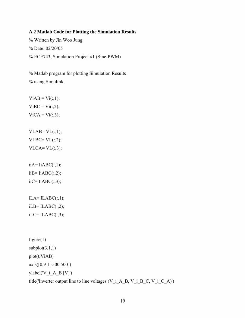
A.2 Matlab Code for Plotting the Simulation Results
% Written by Jin Woo Jung
% Date: 02/20/05
% ECE743, Simulation Project #1 (Sine-PWM)
% Matlab program for plotting Simulation Results
% using Simulink
ViAB = Vi(:,1);
ViBC = Vi(:,2);
ViCA = Vi(:,3);
VLAB= VL(:,1);
VLBC= VL(:,2);
VLCA= VL(:,3);
iiA= IiABC(:,1);
iiB= IiABC(:,2);
iiC= IiABC(:,3);
iLA= ILABC(:,1);
iLB= ILABC(:,2);
iLC= ILABC(:,3);
figure(1)
subplot(3,1,1)
plot(t,ViAB)
axis([0.9 1 -500 500])
ylabel('V_i_A_B [V]')
title('Inverter output line to line voltages (V_i_A_B, V_i_B_C, V_i_C_A)')

20
grid
subplot(3,1,2)
plot(t,ViBC)
axis([0.9 1 -500 500])
ylabel('V_i_B_C [V]')
grid
subplot(3,1,3)
plot(t,ViCA)
axis([0.9 1 -500 500])
ylabel('V_i_C_A [V]')
xlabel('Time [Sec]')
grid
figure(2)
subplot(3,1,1)
plot(t,iiA)
axis([0.9 1 -100 100])
ylabel('i_i_A [A]')
title('Inverter output currents (i_i_A, i_i_B, i_i_C)')
grid
subplot(3,1,2)
plot(t,iiB)
axis([0.9 1 -100 100])
ylabel('i_i_B [A]')
grid
subplot(3,1,3)
21
plot(t,iiC)
axis([0.9 1 -100 100])
ylabel('i_i_C [A]')
xlabel('Time [Sec]')
grid
figure(3)
subplot(3,1,1)
plot(t,VLAB)
axis([0.9 1 -400 400])
ylabel('V_L_A_B [V]')
title('Load line to line voltages (V_L_A_B, V_L_B_C, V_L_C_A)')
grid
subplot(3,1,2)
plot(t,VLBC)
axis([0.9 1 -400 400])
ylabel('V_L_B_C [V]')
grid
subplot(3,1,3)
plot(t,VLCA)
axis([0.9 1 -400 400])
ylabel('V_L_C_A [V]')
xlabel('Time [Sec]')
grid
figure(4)
subplot(3,1,1)
plot(t,iLA)
axis([0.9 1 -50 50])

22
ylabel('i_L_A [A]')
title('Load phase currents (i_L_A, i_L_B, i_L_C)')
grid
subplot(3,1,2)
plot(t,iLB)
axis([0.9 1 -50 50])
ylabel('i_L_B [A]')
grid
subplot(3,1,3)
plot(t,iLC)
axis([0.9 1 -50 50])
ylabel('i_L_C [A]')
xlabel('Time [Sec]')
grid
figure(5)
subplot(4,1,1)
plot(t,ViAB)
axis([0.9 1 -500 500])
ylabel('V_i_A_B [V]')
grid
subplot(4,1,2)
plot(t,iiA,'-', t,iiB,'-.',t,iiC,':')
axis([0.9 1 -100 100])
ylabel('i_i_A, i_i_B, i_i_C [A]')
legend('i_i_A', 'i_i_B', 'i_i_C')
grid

23
subplot(4,1,3)
plot(t,VLAB,'-', t,VLBC,'-.',t,VLCA,':')
axis([0.9 1 -400 400])
ylabel('V_L_A_B, V_L_B_C, V_L_C_A [V]')
legend('V_L_A_B', 'V_L_B_C', 'V_L_C_A')
grid
subplot(4,1,4)
plot(t,iLA,'-', t,iLB,'-.',t,iLC,':')
axis([0.9 1 -50 50])
ylabel('i_L_A, i_L_B, i_L_C [A]')
legend('i_L_A', 'i_L_B', 'i_L_C')
xlabel('Time [Sec]')
grid
%For only Sine PWM
figure(6)
subplot(4,1,1)
plot(t,Vtri,'-', t,Vsin,'-.')
axis([0.9 0.917 -1.5 1.5])
ylabel('V_t_r_i, V_s_i_n [V]')
legend('V_t_r_i', 'V_s_i_n')
title('V_t_r_i and V_s_i_n')
grid
subplot(4,1,2)
plot(t,ViAn)
axis([0.9 0.917 -500 500])
ylabel('V_i_A_n [V]')
grid

24
subplot(4,1,3)
plot(t,Vtri,'-', t,Vsin,'-.')
axis([0.9 0.909 -1.5 1.5])
ylabel('V_t_r_i, V_s_i_n [V]')
legend('V_t_r_i', 'V_s_i_n')
grid
subplot(4,1,4)
plot(t,ViAn)
axis([0.9 0.909 -500 500])
ylabel('V_i_A_n [V]')
xlabel('Time [Sec]')
grid

25
A.3 Simulink Code
Simulink Model for Overall System

26
Simulink Model for “Sine-PWM Generator”