Embed Size (px)
Citation preview
SINGLE-INDUCTOR MULTIPLE-OUTPUT
DC-DC CONVERTERS
Massimiliano Belloni, Edoardo Bonizzoni, Franco Maloberti University of Pavia
Department of Electronics Via Ferrata, 1 - 27100 Pavia - ITALY
[massimiliano.belloni, edoardo.bonizzoni, franco.maloberti]@unipv.it
Abstract
This chapter deals with the design methodologies to obtain DC-DC converters with multiple outputs and only one inductor. The four possible schemes, buck, boost, and inverting or non-inverting buck-boost, are considered. The key specific problems related to the issue are the inductor current switching scheme, the multiple-loops control, the suitable driving of power switches and, accordingly, the converter power efficiency. All the issues are discussed in details. Moreover, design examples of devices integrated with CMOS technologies and the experimental results are presented.
1. Introduction
The continuous market growth of battery-operated systems and the need of optimizing the power consumption in multi-processors by a dynamic regulation of the supply voltage expand significantly the portable power management market. In addition to conventional DC-DC devices, [1], there is an increasing need of DC-DC converters capable to generate many outputs while using a single inductor. The reason is that when on the same system it is required to generate multiple supply voltages, the increased PCB area, the augmented number of components, and the reduced reliability for the many inductors used, becomes problematic, [2], [3]. The new devices discussed here that can be boost, buck or buck-boost, give the solution. To have multiple outputs it is necessary to time-share the inductor current between various loads. For this, the feedback loop that regulates the voltage becomes a multi-feedback loop with probable problems of stability and possible ringing of the outputs. Moreover, for buck architectures, it is necessary to use extra power switches. In addition, for these kinds of converters, the switches must separate voltages that can have a significantly different value. Therefore, the power switch drivers must account for problems that are specific of the multiple output function.
2. SISO DC-DC Switching Regulators
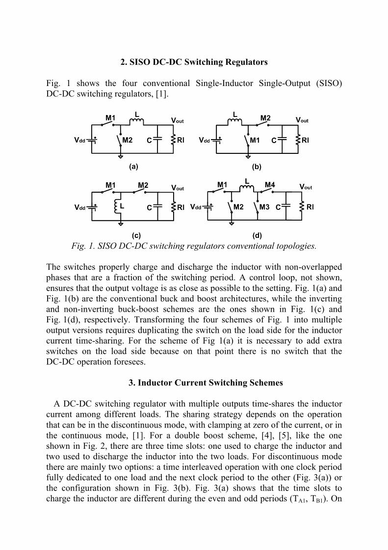
Fig. 1 shows the four conventional Single-Inductor Single-Output (SISO) DC-DC switching regulators, [1].
Fig. 1. SISO DC-DC switching regulators conventional topologies.
The switches properly charge and discharge the inductor with non-overlapped phases that are a fraction of the switching period. A control loop, not shown, ensures that the output voltage is as close as possible to the setting. Fig. 1(a) and Fig. 1(b) are the conventional buck and boost architectures, while the inverting and non-inverting buck-boost schemes are the ones shown in Fig. 1(c) and Fig. 1(d), respectively. Transforming the four schemes of Fig. 1 into multiple output versions requires duplicating the switch on the load side for the inductor current time-sharing. For the scheme of Fig 1(a) it is necessary to add extra switches on the load side because on that point there is no switch that the DC-DC operation foresees.
3. Inductor Current Switching Schemes
A DC-DC switching regulator with multiple outputs time-shares the inductor current among different loads. The sharing strategy depends on the operation that can be in the discontinuous mode, with clamping at zero of the current, or in the continuous mode, [1]. For a double boost scheme, [4], [5], like the one shown in Fig. 2, there are three time slots: one used to charge the inductor and two used to discharge the inductor into the two loads. For discontinuous mode there are mainly two options: a time interleaved operation with one clock period fully dedicated to one load and the next clock period to the other (Fig. 3(a)) or the configuration shown in Fig. 3(b). Fig. 3(a) shows that the time slots to charge the inductor are different during the even and odd periods (TA1, TB1). On
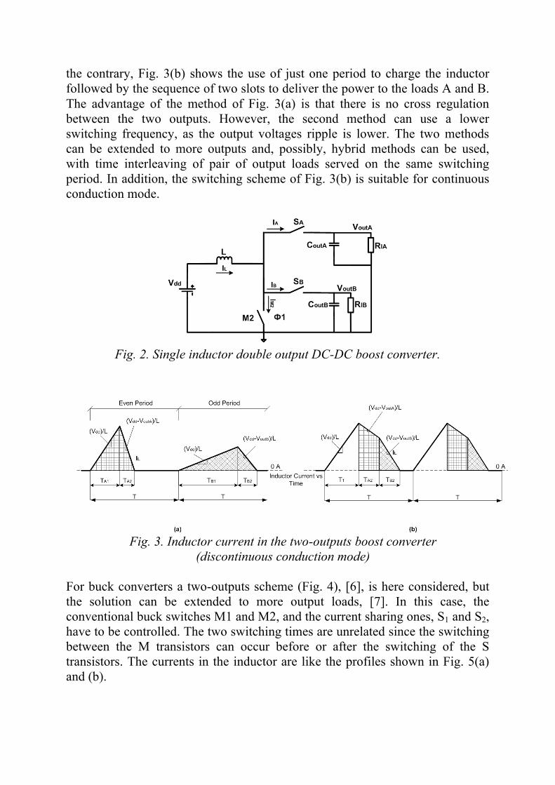
the contrary, Fig. 3(b) shows the use of just one period to charge the inductor followed by the sequence of two slots to deliver the power to the loads A and B. The advantage of the method of Fig. 3(a) is that there is no cross regulation between the two outputs. However, the second method can use a lower switching frequency, as the output voltages ripple is lower. The two methods can be extended to more outputs and, possibly, hybrid methods can be used, with time interleaving of pair of output loads served on the same switching period. In addition, the switching scheme of Fig. 3(b) is suitable for continuous conduction mode.
Fig. 2. Single inductor double output DC-DC boost converter.
Fig. 3. Inductor current in the two-outputs boost converter
(discontinuous conduction mode)
For buck converters a two-outputs scheme (Fig. 4), [6], is here considered, but the solution can be extended to more output loads, [7]. In this case, the conventional buck switches M1 and M2, and the current sharing ones, S1 and S2, have to be controlled. The two switching times are unrelated since the switching between the M transistors can occur before or after the switching of the S transistors. The currents in the inductor are like the profiles shown in Fig. 5(a) and (b).
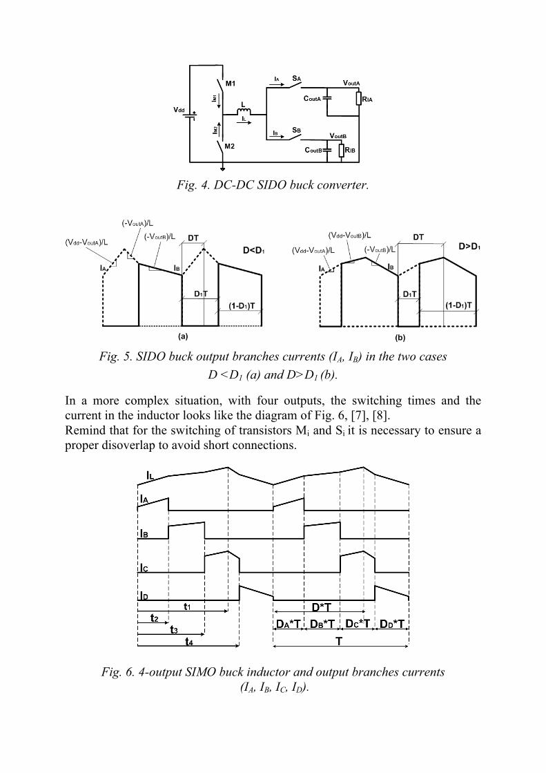
Fig. 4. DC-DC SIDO buck converter.
Fig. 5. SIDO buck output branches currents (IA, IB) in the two cases
D <D1 (a) and D>D1 (b).
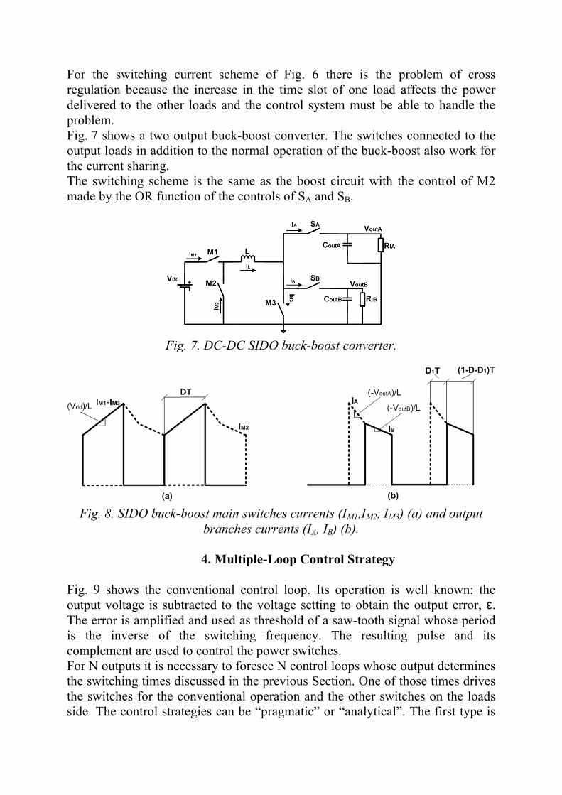
In a more complex situation, with four outputs, the switching times and the current in the inductor looks like the diagram of Fig. 6, [7], [8]. Remind that for the switching of transistors Mi and Si it is necessary to ensure a proper disoverlap to avoid short connections.
Fig. 6. 4-output SIMO buck inductor and output branches currents (IA, IB, IC, ID).
For the switching current scheme of Fig. 6 there is the problem of cross regulation because the increase in the time slot of one load affects the power delivered to the other loads and the control system must be able to handle the problem. Fig. 7 shows a two output buck-boost converter. The switches connected to the output loads in addition to the normal operation of the buck-boost also work for the current sharing. The switching scheme is the same as the boost circuit with the control of M2 made by the OR function of the controls of SA and SB.
Fig. 7. DC-DC SIDO buck-boost converter.
Fig. 8. SIDO buck-boost main switches currents (IM1,IM2, IM3) (a) and output
branches currents (IA, IB) (b).
4. Multiple-Loop Control Strategy
Fig. 9 shows the conventional control loop. Its operation is well known: the output voltage is subtracted to the voltage setting to obtain the output error, ε. The error is amplified and used as threshold of a saw-tooth signal whose period is the inverse of the switching frequency. The resulting pulse and its complement are used to control the power switches. For N outputs it is necessary to foresee N control loops whose output determines the switching times discussed in the previous Section. One of those times drives the switches for the conventional operation and the other switches on the loads side. The control strategies can be “pragmatic” or “analytical”. The first type is
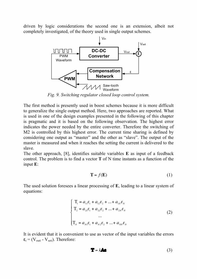
driven by logic considerations the second one is an extension, albeit not completely investigated, of the theory used in single output schemes.
Fig. 9. Switching regulator closed loop control system.
The first method is presently used in boost schemes because it is more difficult to generalize the single output method. Here, two approaches are reported. What is used in one of the design examples presented in the following of this chapter is pragmatic and it is based on the following observation. The highest error indicates the power needed by the entire converter. Therefore the switching of M2 is controlled by this highest error. The current time sharing is defined by considering one output as “master” and the other as “slave”. The output of the master is measured and when it reaches the setting the current is delivered to the slave. The other approach, [8], identifies suitable variables E as input of a feedback control. The problem is to find a vector T of N time instants as a function of the input E:
€
T = f (E) (1) The used solution foresees a linear processing of E, leading to a linear system of equations:
€
T1 = a11ε1 + a12ε2 + ...+ a1NεNT2 = a21ε1 + a22ε2 + ...+ a2NεN
...TN = aN1ε1 + aN 2ε2 + ...+ aNNεN
(2)
It is evident that it is convenient to use as vector of the input variables the errors εi = (Vouti - Vseti). Therefore:
€
Τ = kΑε (3)
where k denotes the overall gain loop. The various used solutions differ because of the utilized matrix A. As an example, the following matrixes can be considered:
€
A =
1 0 ... 0 00 1 ... 0 00 0 ... 0 00 0 ... 1 00 0 ... 0 1
(4)
that is using a single error for the control of one of the times.
€
A =
1 1 1 11 −1 −1 −11 1 −1 −11 1 1 −1
(5)
with the first line used to control the main switching. This solution has proved better performance for buck converters with N > 2. For boost configurations, it is also possible to use the analytical method. It is required to use coefficients that ensure the condition Ti > T1, i>1 (6) where T1 is the charging period.
5. Power Switches Driving
As mentioned above, in multiple-output DC-DC converters, an important design issue is the power switches driving strategy as it affects the overall system effectiveness, in terms both of area and power. In any single or multiple outputs DC-DC converter, the switch connected to the battery and the one connected to ground are obviously made by p-channel and n-channel devices, respectively. By contrast, the switches on the load side can be problematic. There are three possibilities: use of a p-channel, an n-channel or a complementary switch. The choice depends on the expected regulated voltage, and the cost-efficiency trade off. If the regulated voltage is relatively large, much higher than the transistor threshold, then the use of a p-channel is a good solution: the overdrive is enough and the series conductance, Gon, caused by the extra switch can become affordable with a reasonable transistor aspect ratio
€
Gon = µCox
WLVout −VTh( ) (7)
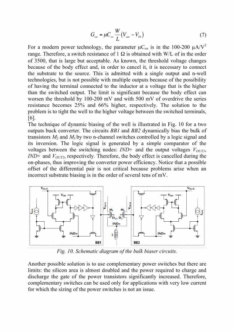
For a modern power technology, the parameter µCox is in the 100-200 µA/V2 range. Therefore, a switch resistance of 1 Ω is obtained with W/L of in the order of 3500, that is large but acceptable. As known, the threshold voltage changes because of the body effect and, in order to cancel it, it is necessary to connect the substrate to the source. This is admitted with a single output and n-well technologies, but is not possible with multiple outputs because of the possibility of having the terminal connected to the inductor at a voltage that is the higher than the switched output. The limit is significant because the body effect can worsen the threshold by 100-200 mV and with 500 mV of overdrive the series resistance becomes 25% and 66% higher, respectively. The solution to the problem is to tight the well to the higher voltage between the switched terminals, [6]. The technique of dynamic biasing of the well is illustrated in Fig. 10 for a two outputs buck converter. The circuits BB1 and BB2 dynamically bias the bulk of transistors M2 and M3 by two n-channel switches controlled by a logic signal and its inversion. The logic signal is generated by a simple comparator of the voltages between the switching nodes: IND+ and the output voltages VOUT1, IND+ and VOUT2, respectively. Therefore, the body effect is cancelled during the on-phases, thus improving the converter power efficiency. Notice that a possible offset of the differential pair is not critical because problems arise when an incorrect substrate biasing is in the order of several tens of mV.
Fig. 10. Schematic diagram of the bulk biaser circuits.
Another possible solution is to use complementary power switches but there are limits: the silicon area is almost doubled and the power required to charge and discharge the gate of the power transistors significantly increased. Therefore, complementary switches can be used only for applications with very low current for which the sizing of the power switches is not an issue.
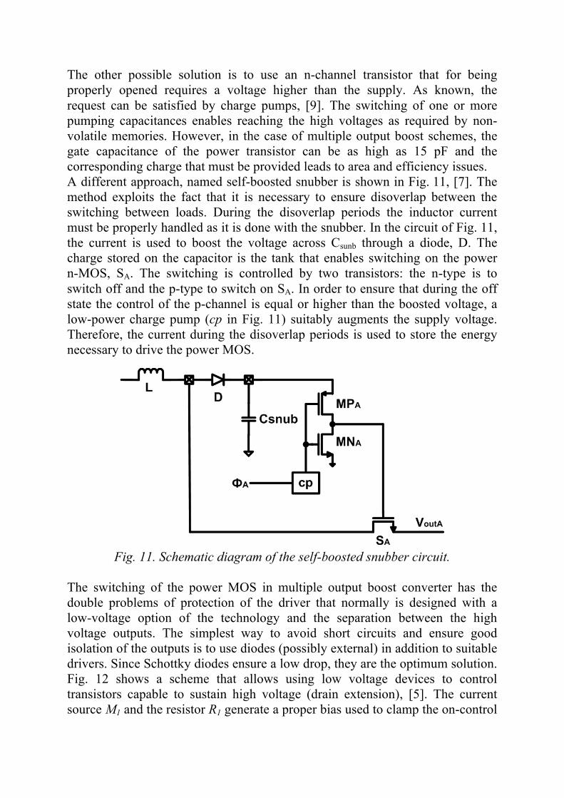
The other possible solution is to use an n-channel transistor that for being properly opened requires a voltage higher than the supply. As known, the request can be satisfied by charge pumps, [9]. The switching of one or more pumping capacitances enables reaching the high voltages as required by non-volatile memories. However, in the case of multiple output boost schemes, the gate capacitance of the power transistor can be as high as 15 pF and the corresponding charge that must be provided leads to area and efficiency issues. A different approach, named self-boosted snubber is shown in Fig. 11, [7]. The method exploits the fact that it is necessary to ensure disoverlap between the switching between loads. During the disoverlap periods the inductor current must be properly handled as it is done with the snubber. In the circuit of Fig. 11, the current is used to boost the voltage across Csunb through a diode, D. The charge stored on the capacitor is the tank that enables switching on the power n-MOS, SA. The switching is controlled by two transistors: the n-type is to switch off and the p-type to switch on SA. In order to ensure that during the off state the control of the p-channel is equal or higher than the boosted voltage, a low-power charge pump (cp in Fig. 11) suitably augments the supply voltage. Therefore, the current during the disoverlap periods is used to store the energy necessary to drive the power MOS.
Fig. 11. Schematic diagram of the self-boosted snubber circuit.
The switching of the power MOS in multiple output boost converter has the double problems of protection of the driver that normally is designed with a low-voltage option of the technology and the separation between the high voltage outputs. The simplest way to avoid short circuits and ensure good isolation of the outputs is to use diodes (possibly external) in addition to suitable drivers. Since Schottky diodes ensure a low drop, they are the optimum solution. Fig. 12 shows a scheme that allows using low voltage devices to control transistors capable to sustain high voltage (drain extension), [5]. The current source M1 and the resistor R1 generate a proper bias used to clamp the on-control
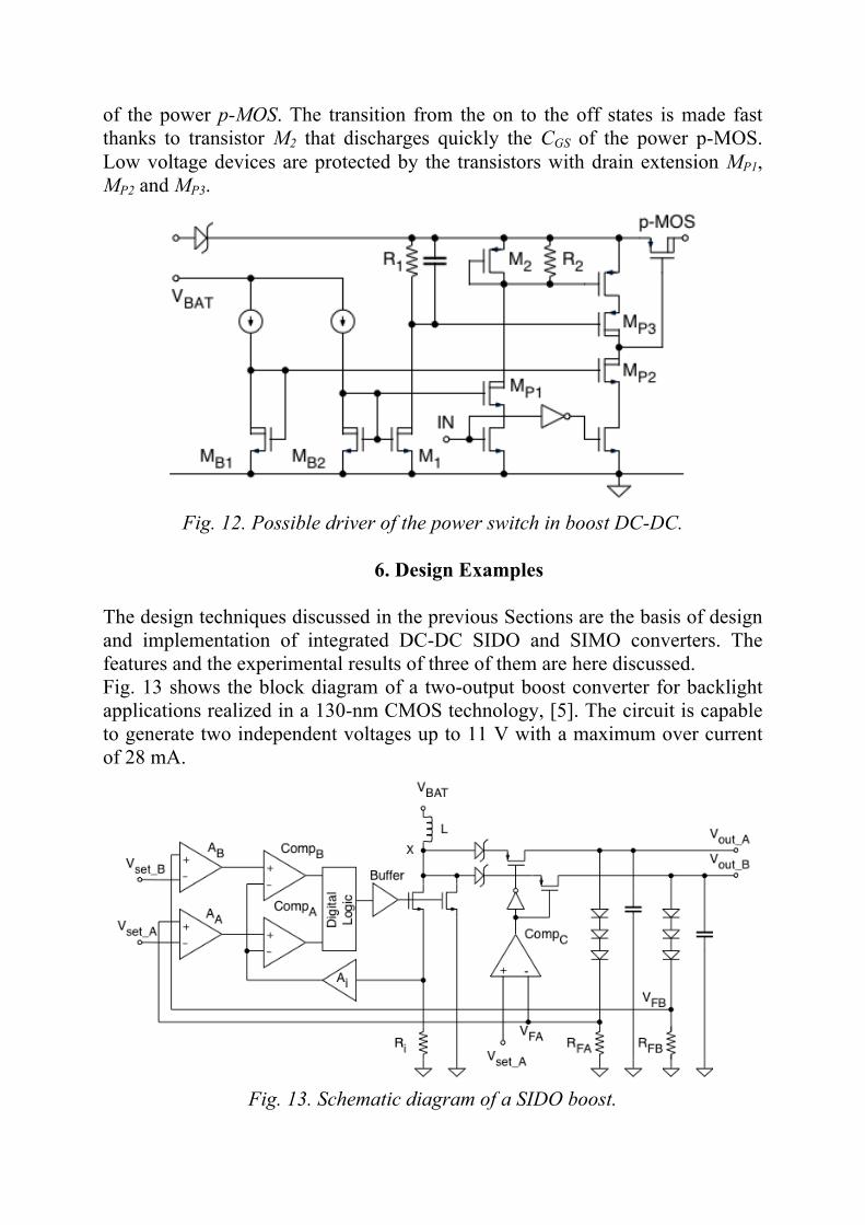
of the power p-MOS. The transition from the on to the off states is made fast thanks to transistor M2 that discharges quickly the CGS of the power p-MOS. Low voltage devices are protected by the transistors with drain extension MP1, MP2 and MP3.
Fig. 12. Possible driver of the power switch in boost DC-DC.
6. Design Examples
The design techniques discussed in the previous Sections are the basis of design and implementation of integrated DC-DC SIDO and SIMO converters. The features and the experimental results of three of them are here discussed. Fig. 13 shows the block diagram of a two-output boost converter for backlight applications realized in a 130-nm CMOS technology, [5]. The circuit is capable to generate two independent voltages up to 11 V with a maximum over current of 28 mA.
Fig. 13. Schematic diagram of a SIDO boost.
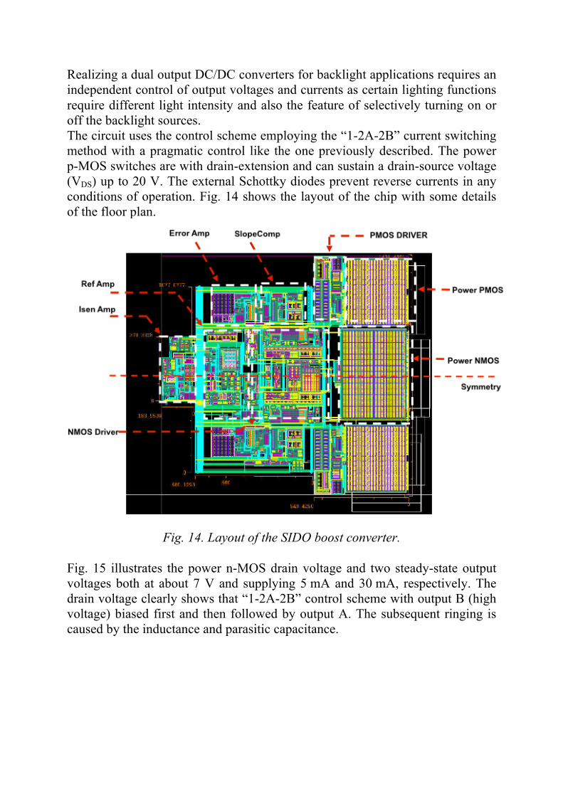
Realizing a dual output DC/DC converters for backlight applications requires an independent control of output voltages and currents as certain lighting functions require different light intensity and also the feature of selectively turning on or off the backlight sources. The circuit uses the control scheme employing the “1-2A-2B” current switching method with a pragmatic control like the one previously described. The power p-MOS switches are with drain-extension and can sustain a drain-source voltage (VDS) up to 20 V. The external Schottky diodes prevent reverse currents in any conditions of operation. Fig. 14 shows the layout of the chip with some details of the floor plan.
Fig. 14. Layout of the SIDO boost converter.
Fig. 15 illustrates the power n-MOS drain voltage and two steady-state output voltages both at about 7 V and supplying 5 mA and 30 mA, respectively. The drain voltage clearly shows that “1-2A-2B” control scheme with output B (high voltage) biased first and then followed by output A. The subsequent ringing is caused by the inductance and parasitic capacitance.
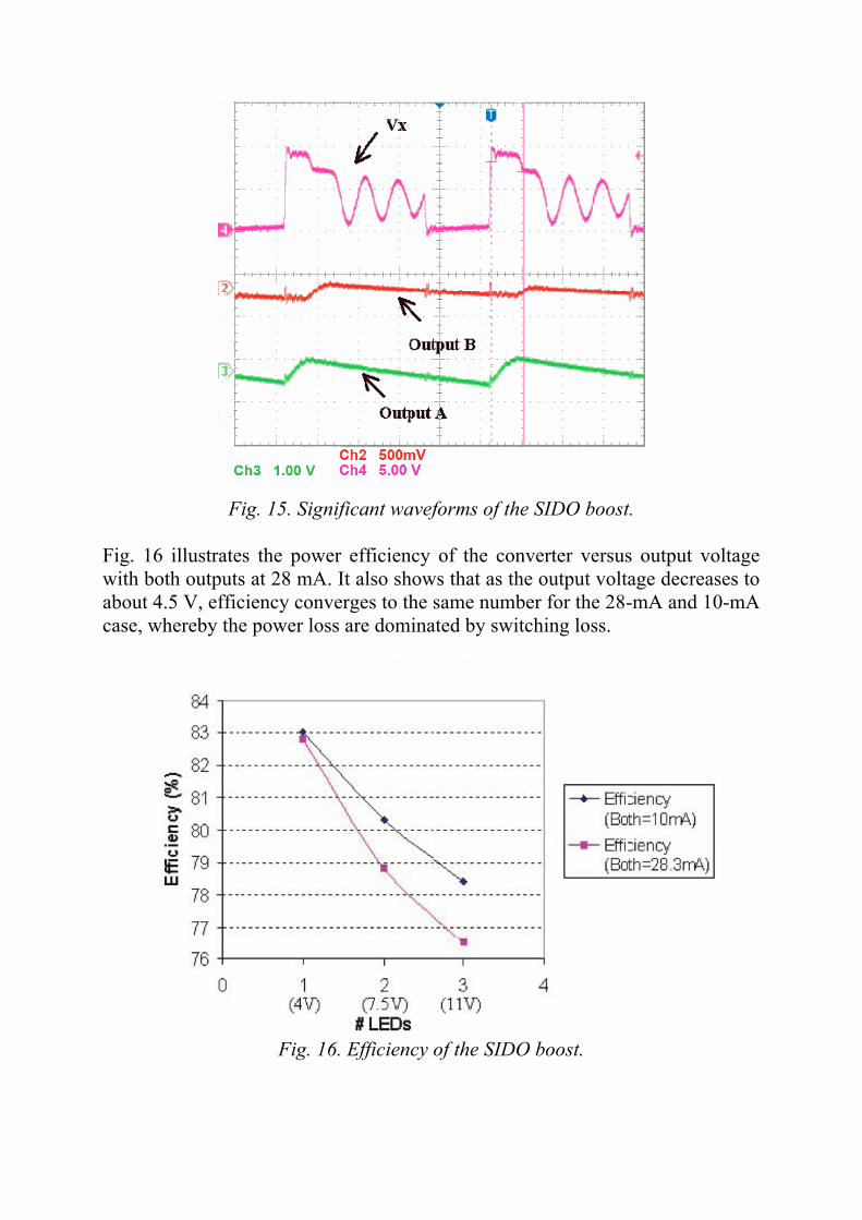
Fig. 15. Significant waveforms of the SIDO boost.
Fig. 16 illustrates the power efficiency of the converter versus output voltage with both outputs at 28 mA. It also shows that as the output voltage decreases to about 4.5 V, efficiency converges to the same number for the 28-mA and 10-mA case, whereby the power loss are dominated by switching loss.
Fig. 16. Efficiency of the SIDO boost.
The second design example is a two-output buck, [6]. Its basic scheme is shown in Fig. 17. The loop control is a simple diagonal coefficient matrix: the control of the main switching is done with one of the errors and the time-sharing with the other.
Fig. 17. Circuit diagram of the proposed SIDO buck.
The PWM generator uses the same waveform (in this case a triangular wave) to obtain both the control phases. The switching frequency is 1 MHz and the gain of the error ensured by A1 and A2 is approximately 45 dB. Switches S1 and S4 are obviously realized with n-channel and p-channel devices, respectively. Since it is assumed that the regulated voltage is relatively high, S2 and S3 are p-channel devices. The sizes of M1, M2, and M3are equal to 18000/0.6 µm, while NMOS transistor M4 is 6000/0.6 µm. These aspect ratios come up from a trade-off between the on-resistance of the switches, the waste of silicon area, and the dynamic power consumption. The used channel length (about twice the minimum) minimizes transistor leakage currents and ensures proper ESD protection. The circuit achieves the optimum substrate biasing by the dynamically switch between the voltages across the switch terminals, as discussed in the previous section. The single-inductor dual-output buck converter has been fabricated in a 0.35-µm, 5-V transistor option, p-substrate, 2-poly, 3-metal levels CMOS technology. Fig. 18 shows the chip microphotograph. The chip area is 1350 µm x 1800 µm, including pads. The power transistor area is about 0.22 mm2. In order to minimize the resistance and the inductance of the bonding wires, a triple bonding approach has been adopted for the drain and the source
terminals of each power transistor. The used off-chip inductor and storage capacitors, referred to as L, C1, and C2, respectively, are 22 µH and 35 µF, respectively.
Fig. 18. Chip microphotograph.
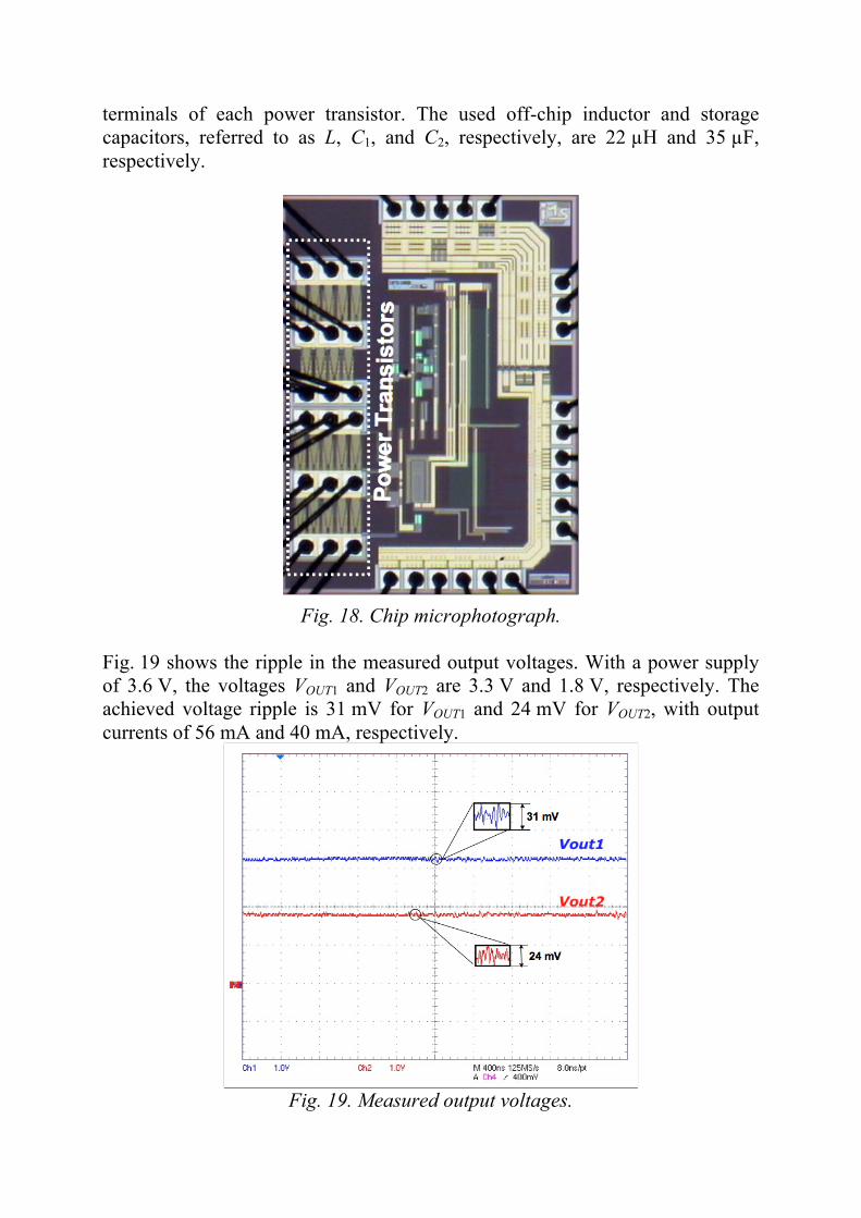
Fig. 19 shows the ripple in the measured output voltages. With a power supply of 3.6 V, the voltages VOUT1 and VOUT2 are 3.3 V and 1.8 V, respectively. The achieved voltage ripple is 31 mV for VOUT1 and 24 mV for VOUT2, with output currents of 56 mA and 40 mA, respectively.
Fig. 19. Measured output voltages.
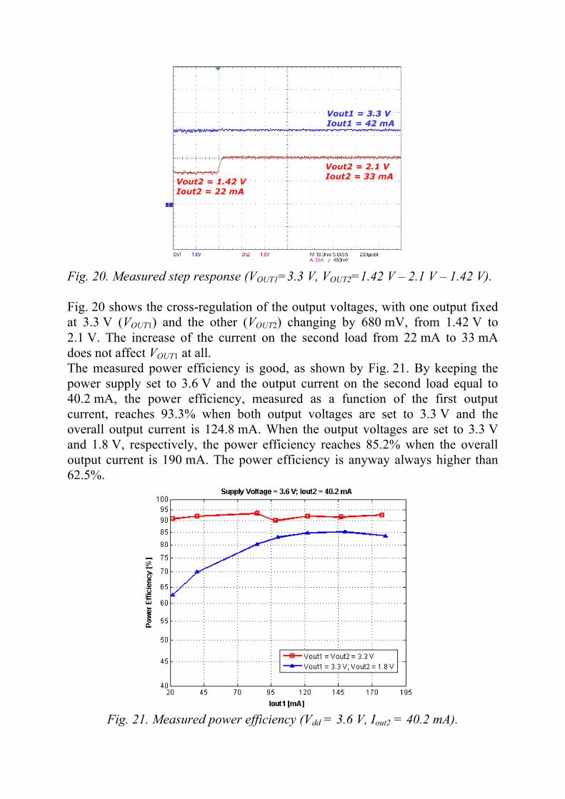
Fig. 20. Measured step response (VOUT1=3.3 V, VOUT2=1.42 V – 2.1 V – 1.42 V). Fig. 20 shows the cross-regulation of the output voltages, with one output fixed at 3.3 V (VOUT1) and the other (VOUT2) changing by 680 mV, from 1.42 V to 2.1 V. The increase of the current on the second load from 22 mA to 33 mA does not affect VOUT1 at all. The measured power efficiency is good, as shown by Fig. 21. By keeping the power supply set to 3.6 V and the output current on the second load equal to 40.2 mA, the power efficiency, measured as a function of the first output current, reaches 93.3% when both output voltages are set to 3.3 V and the overall output current is 124.8 mA. When the output voltages are set to 3.3 V and 1.8 V, respectively, the power efficiency reaches 85.2% when the overall output current is 190 mA. The power efficiency is anyway always higher than 62.5%.
Fig. 21. Measured power efficiency (Vdd = 3.6 V, Iout2 = 40.2 mA).
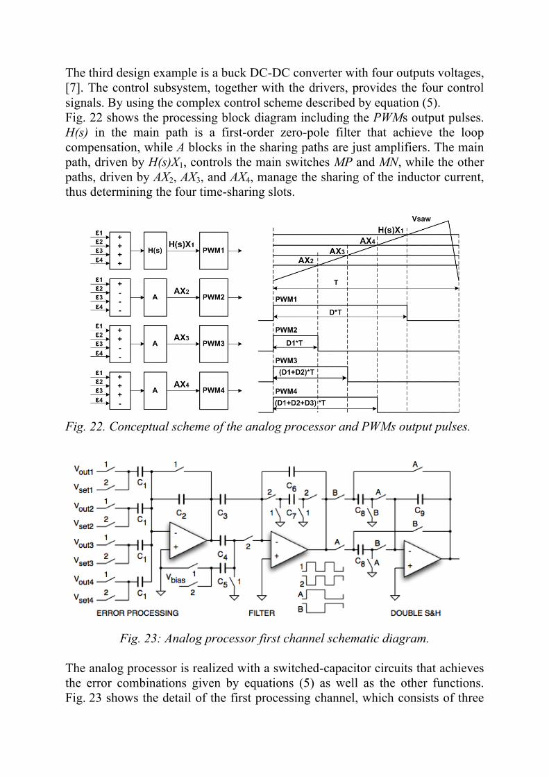
The third design example is a buck DC-DC converter with four outputs voltages, [7]. The control subsystem, together with the drivers, provides the four control signals. By using the complex control scheme described by equation (5). Fig. 22 shows the processing block diagram including the PWMs output pulses. H(s) in the main path is a first-order zero-pole filter that achieve the loop compensation, while A blocks in the sharing paths are just amplifiers. The main path, driven by H(s)X1, controls the main switches MP and MN, while the other paths, driven by AX2, AX3, and AX4, manage the sharing of the inductor current, thus determining the four time-sharing slots.
Fig. 22. Conceptual scheme of the analog processor and PWMs output pulses.
Fig. 23: Analog processor first channel schematic diagram.
The analog processor is realized with a switched-capacitor circuits that achieves the error combinations given by equations (5) as well as the other functions. Fig. 23 shows the detail of the first processing channel, which consists of three
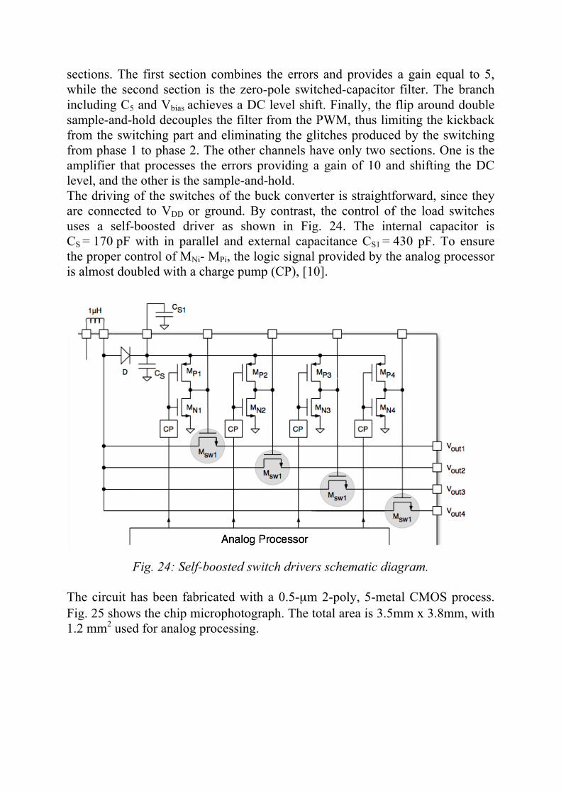
sections. The first section combines the errors and provides a gain equal to 5, while the second section is the zero-pole switched-capacitor filter. The branch including C5 and Vbias achieves a DC level shift. Finally, the flip around double sample-and-hold decouples the filter from the PWM, thus limiting the kickback from the switching part and eliminating the glitches produced by the switching from phase 1 to phase 2. The other channels have only two sections. One is the amplifier that processes the errors providing a gain of 10 and shifting the DC level, and the other is the sample-and-hold. The driving of the switches of the buck converter is straightforward, since they are connected to VDD or ground. By contrast, the control of the load switches uses a self-boosted driver as shown in Fig. 24. The internal capacitor is CS = 170 pF with in parallel and external capacitance CS1 = 430 pF. To ensure the proper control of MNi- MPi, the logic signal provided by the analog processor is almost doubled with a charge pump (CP), [10].
Fig. 24: Self-boosted switch drivers schematic diagram.
The circuit has been fabricated with a 0.5-µm 2-poly, 5-metal CMOS process. Fig. 25 shows the chip microphotograph. The total area is 3.5mm x 3.8mm, with 1.2 mm2 used for analog processing.
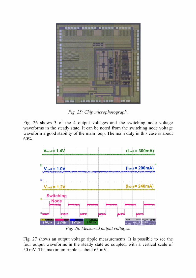
Fig. 25: Chip microphotograph. Fig. 26 shows 3 of the 4 output voltages and the switching node voltage waveforms in the steady state. It can be noted from the switching node voltage waveform a good stability of the main loop. The main duty in this case is about 60%.
Fig. 26. Measured output voltages.
Fig. 27 shows an output voltage ripple measurements. It is possible to see the four output waveforms in the steady state ac coupled, with a vertical scale of 50 mV. The maximum ripple is about 65 mV.
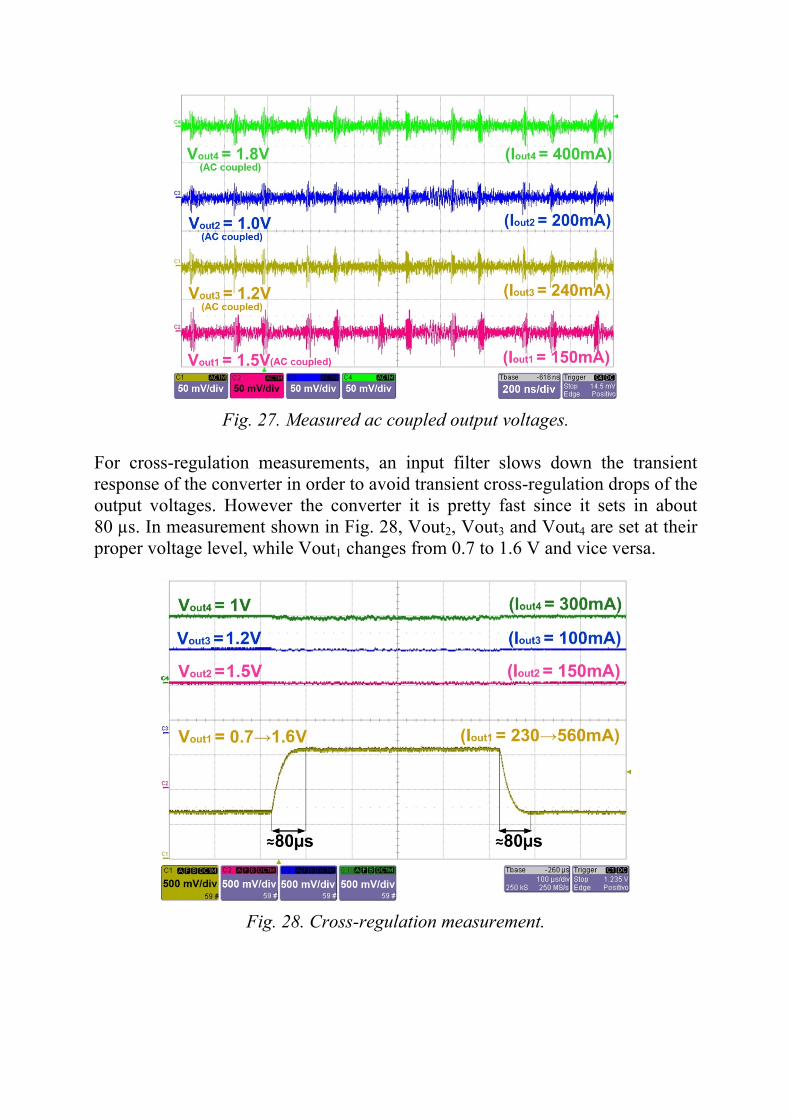
Fig. 27. Measured ac coupled output voltages.
For cross-regulation measurements, an input filter slows down the transient response of the converter in order to avoid transient cross-regulation drops of the output voltages. However the converter it is pretty fast since it sets in about 80 µs. In measurement shown in Fig. 28, Vout2, Vout3 and Vout4 are set at their proper voltage level, while Vout1 changes from 0.7 to 1.6 V and vice versa.
Fig. 28. Cross-regulation measurement.
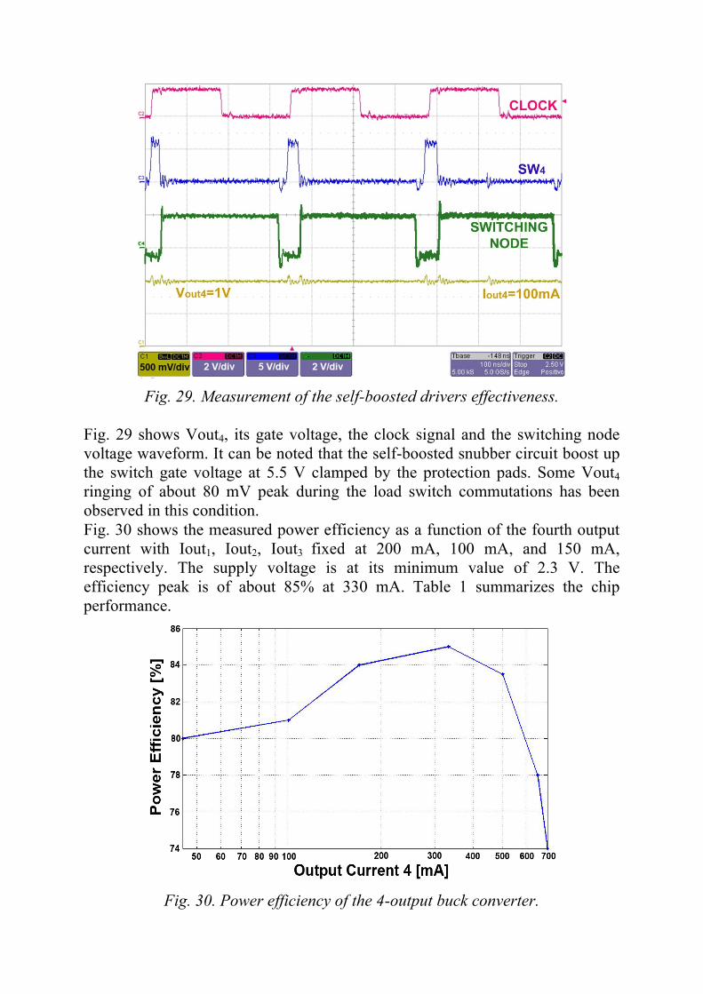
Fig. 29. Measurement of the self-boosted drivers effectiveness.
Fig. 29 shows Vout4, its gate voltage, the clock signal and the switching node voltage waveform. It can be noted that the self-boosted snubber circuit boost up the switch gate voltage at 5.5 V clamped by the protection pads. Some Vout4 ringing of about 80 mV peak during the load switch commutations has been observed in this condition. Fig. 30 shows the measured power efficiency as a function of the fourth output current with Iout1, Iout2, Iout3 fixed at 200 mA, 100 mA, and 150 mA, respectively. The supply voltage is at its minimum value of 2.3 V. The efficiency peak is of about 85% at 330 mA. Table 1 summarizes the chip performance.
Fig. 30. Power efficiency of the 4-output buck converter.
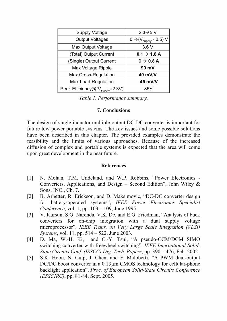
Table 1. Performance summary.
7. Conclusions
The design of single-inductor multiple-output DC-DC converter is important for future low-power portable systems. The key issues and some possible solutions have been described in this chapter. The provided examples demonstrate the feasibility and the limits of various approaches. Because of the increased diffusion of complex and portable systems is expected that the area will come upon great development in the near future.
References [1] N. Mohan, T.M. Undeland, and W.P. Robbins, “Power Electronics -
Converters, Applications, and Design – Second Edition”, John Wiley & Sons, INC., Ch. 7.
[2] B. Arbetter, R. Erickson, and D. Maksimovic, “DC-DC converter design for battery-operated systems”, IEEE Power Electronics Specialist Conference, vol. 1, pp. 103 – 109, June 1995.
[3] V. Kursun, S.G. Narenda, V.K. De, and E.G. Friedman, “Analysis of buck converters for on-chip integration with a dual supply voltage microprocessor”, IEEE Trans. on Very Large Scale Integration (VLSI) Systems, vol. 11, pp. 514 – 522, June 2003.
[4] D. Ma, W.-H. Ki, and C.-Y. Tsui, “A pseudo-CCM/DCM SIMO switching converter with freewheel switching”, IEEE International Solid-State Circuits Conf. (ISSCC) Dig. Tech. Papers, pp. 390 – 476, Feb. 2002.
[5] S.K. Hoon, N. Culp, J. Chen, and F. Maloberti, “A PWM dual-output DC/DC boost converter in a 0.13µm CMOS technology for cellular-phone backlight application”, Proc. of European Solid-State Circuits Conference (ESSCIRC), pp. 81-84, Sept. 2005.
[6] E. Bonizzoni, F. Borghetti, P. Malcovati, F. Maloberti, and B. Niessen, “A 200mA 93% Peak Efficiency Single-Inductor Dual-Output DC-DC Buck Converter”, IEEE International Solid-State Circuits Conf. (ISSCC) Dig. Tech. Papers, pp. 526 – 619, Feb. 2007.
[7] M. Belloni, E. Bonizzoni, E. Kiseliovas, P. Malcovati, F. Maloberti, T. Peltola, and T. Teppo, “A 1.2A Output Current Single-Inductor 4-Outputs DC-DC Buck Converter with Self-Boosted Switch Drivers”, IEEE International Solid-State Circuits Conf. (ISSCC) Dig. Tech. Papers, pp. 444–626, Feb. 2008.
[8] M. Belloni, E. Bonizzoni, and F. Maloberti, “On the Design of Single-Inductor Multiple-Output DC-DC Buck Converters”, to appear in Proc. of 2008 International Symposium on Circuit and Systems (ISCAS).
[9] J. Dickson, “On-chip high voltage generation in NMOS integrated circuits using an improved voltage multiplier technique”, IEEE J. Solid-State Circuits, vol. SC-11, no. 3, pp. 374-378, June 1976.
[10] P. Favrat, P. Deval, and M.J. Declercq, “A new high efficiency CMOS voltage doubler”, Proc. of IEEE Custom Integrated Circuits Conference (CICC), pp. 259 – 262, May 1997.


![Performance Analysis Of High Step-Up DC-DC Converters · PDF fileusing high step up DC-DC converters. ... Inductor Boost Converter (CIBC)[9] using MATLAB simulation. TBC has an advantageover](https://img.pdfslide.net/doc/110x75/5ab156797f8b9a1d168c7548/performance-analysis-of-high-step-up-dc-dc-converters-high-step-up-dc-dc-converters.jpg)