Embed Size (px)
Citation preview
SL811HS Embedded USB Host/Slave Controller
SL811HS
Cypress Semiconductor Corporation • 3901 North First Street • San Jose, CA 95134 • 408-943-2600Document 38-08008 Rev. *B Revised June 13, 2005
1.0 Features• The first USB Host/Slave controller for embedded systems
in the market with a standard microprocessor bus interface.• Supports both full-speed (12 Mbps) and low-speed (1.5
Mbps) USB transfer in both master and slave modes• Conforms to USB Specification 1.1 for Full- and Low-speed• Operates as a single USB host or slave under software
control• Automatic detection of either low or full-speed devices• 8-bit bidirectional data, port I/O (DMA supported in slave
mode) • On-chip SIE and USB transceivers• On-chip single root HUB support• 256-byte internal SRAM buffer• Ping-pong buffers for improved performance• Operates from 12- or 48-MHz crystal or oscillator (built-in
DPLL)• 5V-tolerant interface • Suspend/resume, wake up, and low-power modes are
supported• Auto-generation of SOF and CRC5/16• Auto-address increment mode, saves memory Read/Write
cycles • Development kit including source code drivers is available• Backward-compatible with SL11H, both pin and function-
ality• 3.3V power source, 0.35 micron CMOS technology• Available in both a 28-pin PLCC package (SL811HS) and
a 48-pin TQFP package (SL811HST-AC).
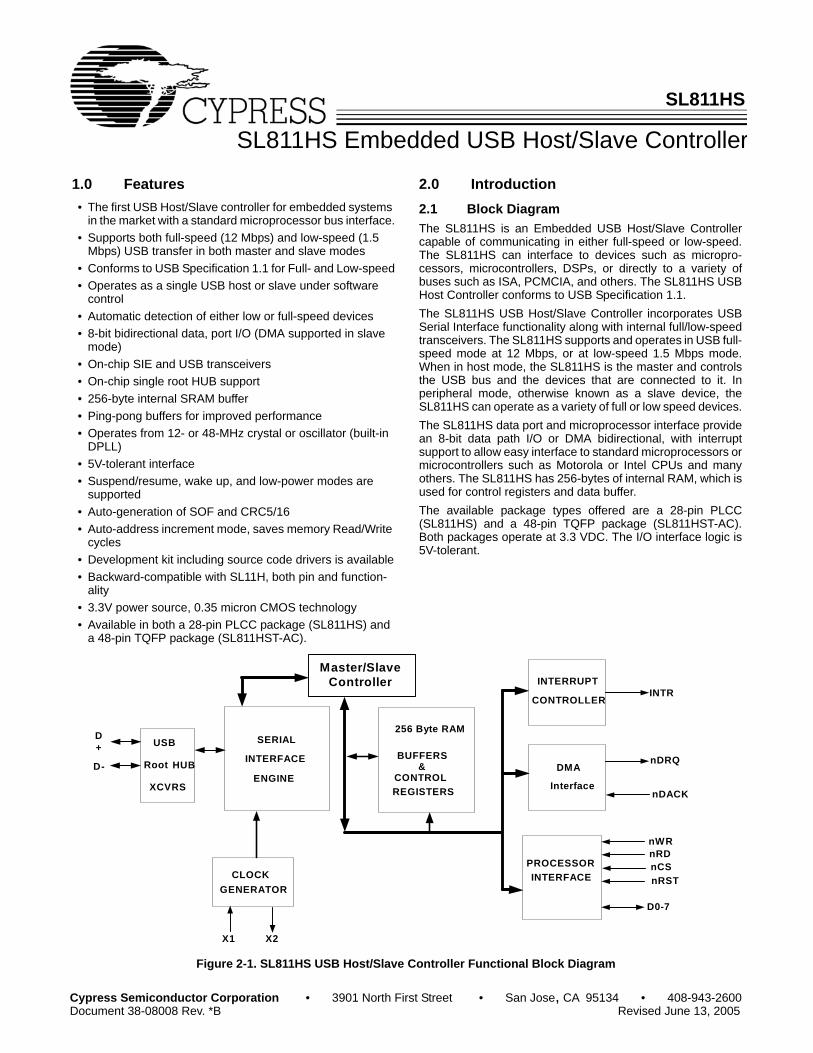
2.0 Introduction2.1 Block DiagramThe SL811HS is an Embedded USB Host/Slave Controllercapable of communicating in either full-speed or low-speed.The SL811HS can interface to devices such as micropro-cessors, microcontrollers, DSPs, or directly to a variety ofbuses such as ISA, PCMCIA, and others. The SL811HS USBHost Controller conforms to USB Specification 1.1.The SL811HS USB Host/Slave Controller incorporates USBSerial Interface functionality along with internal full/low-speedtransceivers. The SL811HS supports and operates in USB full-speed mode at 12 Mbps, or at low-speed 1.5 Mbps mode.When in host mode, the SL811HS is the master and controlsthe USB bus and the devices that are connected to it. Inperipheral mode, otherwise known as a slave device, theSL811HS can operate as a variety of full or low speed devices.The SL811HS data port and microprocessor interface providean 8-bit data path I/O or DMA bidirectional, with interruptsupport to allow easy interface to standard microprocessors ormicrocontrollers such as Motorola or Intel CPUs and manyothers. The SL811HS has 256-bytes of internal RAM, which isused for control registers and data buffer.The available package types offered are a 28-pin PLCC(SL811HS) and a 48-pin TQFP package (SL811HST-AC).Both packages operate at 3.3 VDC. The I/O interface logic is5V-tolerant.
X1 X2
D+
D-
INTR
nWRnRDnCSnRST
D0-7
GENERATOR
USB
Root HUB
XCVRS
SERIAL
INTERFACE
ENGINE
256 Byte RAM
BUFFERS
CONTROLREGISTERS
INTERRUPT
CLOCK
&
CONTROLLER
PROCESSORINTERFACE
Master/SlaveController
nDRQ
nDACK
DMA
Interface
Figure 2-1. SL811HS USB Host/Slave Controller Functional Block Diagram
SL811HS
Document 38-08008 Rev. *B Page 2 of 32
2.2 Data Port, Microprocessor InterfaceThe SL811HS microprocessor interface provides an 8-bitbidirectional data path along with appropriate control lines tointerface to external processors or controllers. ProgrammedI/O or memory mapped I/O designs are supported through the8-bit interface, chip select, read and write input strobes and asingle address line, A0.Access to memory and control register space is a simple twostep process, requiring an address Write with A0 = “0,”followed by a register/memory Read or Write cycle withaddress line A0 = “1.” In addition, a DMA bi-directional interface in slave mode isavailable with handshake signals such as nDRQ, nDACK,nWR, nRD, nCS and INTRQ. The SL811HS Write or Read operation terminates when eithernWR or nCS goes inactive. For devices interfacing to theSL811HS that deactivate the Chip Select nCS before the WritenWR, the data hold timing should be measured from the nCSand will be the same value as specified. Thus, both Intel®- andMotorola-type CPUs can work easily with the SL811HSwithout any external glue logic requirements.
2.3 DMA Controller (slave mode only)In applications that require transfers of large amounts of datasuch as scanner interfaces, the SL811HS provides a DMA in-terface. This interface supports DMA read or write transfers tothe SL811HS internal RAM buffer through the microprocessordata bus via two control lines (nDRQ - Data Request andnDACK - Data Acknowledge) along with the nWR line and con-trols the data flow into the SL811HS. The SL811HS has acount register that allows programmable block sizes to be se-lected for DMA transfer. The control signals, both nDRQ andnDACK, are designed to be compatible with standard DMAinterfaces.
2.4 Interrupt ControllerThe SL811HS interrupt controller provides a single outputsignal (INTRQ) that can be activated by a number of program-mable events that may occur as result of USB activity. Controland status registers are provided to allow the user to selectsingle or multiple events, which will generate an interrupt(assert INTRQ), and let the user view interrupt status. Theinterrupts can be cleared by writing to the appropriate register(the Interrupt Status Register).
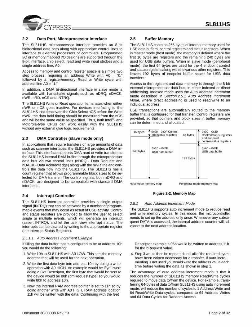
2.5 Buffer MemoryThe SL811HS contains 256 bytes of internal memory used forUSB data buffers, control registers and status registers. Whenin master mode (host mode), the memory is defined where thefirst 16 bytes are registers and the remaining 240 bytes areused for USB data buffers. When in slave mode (peripheralmode), the first 64 bytes are used for the 4 endpoint controland status registers along with the various other registers. Thisleaves 192 bytes of endpoint buffer space for USB datatransfers.Access to the registers and data memory is through the 8-bitexternal microprocessor data bus, in either indexed or directaddressing. Indexed mode uses the Auto Address Incrementmode described in Section 2.5.1 Auto Address IncrementMode, where direct addressing is used to read/write to anindividual address. USB transactions are automatically routed to the memorybuffer that is configured for that transfer. Control registers areprovided, so that pointers and block sizes in buffer memorycan be determined and allocated.
2.5.1 Auto Address Increment ModeThe SL811HS supports auto increment mode to reduce readand write memory cycles. In this mode, the microcontrollerneeds to set up the address only once. Whenever any subse-quent DATA is accessed, the internal address counter will ad-vance to the next address location.
2.5.1.1 Auto Address Increment ExampleIf filling the data buffer that is configured to be at address 10hyou would do the following:1. Write 10h to SL811HS with A0 LOW. This sets the memory
address that will be used for the next operation.2. Write the first data byte into address 10h by doing a write
operation with A0 HIGH. An example would be if you were doing a Get Descriptor, the first byte that would be sent to the device would be 80h (bmRequestType) so you would write 80h to address 10h.
3. Now the internal RAM address pointer is set to 11h so by doing another write with A0 HIGH, RAM address location 11h will be written with the data. Continuing with the Get
Descriptor example a 06h would be written to address 11h for the bRequest value.
4. Step 3 would then be repeated until all of the required bytes have been written necessary for a transfer. If auto-incre-menting is not used you would write the address value each time before writing the data as shown in step 1.
The advantage of auto address increment mode is that itreduces the number of SL811HS memory Read/Write cyclesrequired to move data to/from the device. For example, trans-ferring 64-bytes of data to/from SL811HS using auto incrementmode, will reduce the number of cycles to 1 Address Write and64 Read/Write Data cycles, compared to 64 Address Writesand 64 Data Cycles for Random Access.
0x00 – 0x0F Controland status registers
0x10 – 0xFFUSB data buffer240 bytes
16 bytes 0x00 – 0x39Control/status registersand endpointcontrol/status registers
0x40 – 0xFFUSB data buffer
192 bytes
64 bytes
Host mode memory map Peripheral mode memory map
Figure 2-2. Memory Map
SL811HS
Document 38-08008 Rev. *B Page 3 of 32
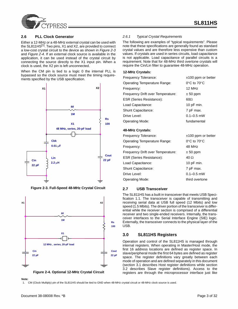
2.6 PLL Clock GeneratorEither a 12-MHz or a 48-MHz external crystal can be used withthe SL811HS[1]. Two pins, X1 and X2, are provided to connecta low-cost crystal circuit to the device as shown in Figure 2-3and Figure 2-4. If an external clock source is available in theapplication, it can be used instead of the crystal circuit byconnecting the source directly to the X1 input pin. When aclock is used, the X2 pin is left unconnected. When the CM pin is tied to a logic 0 the internal PLL isbypassed so the clock source must meet the timing require-ments specified by the USB specification.
2.6.1 Typical Crystal RequirementsThe following are examples of “typical requirements”. Pleasenote that these specifications are generally found as standardcrystal values and are therefore less expensive than customvalues. If crystals are used in series circuits, load capacitanceis not applicable. Load capacitance of parallel circuits is arequirement. Note that for 48-MHz third overtone crystals willrequire the Cin/Lin filter to guarantee 48-MHz operation.
2.7 USB TransceiverThe SL811HS has a built in transceiver that meets USB Speci-fication 1.1. The transceiver is capable of transmitting andreceiving serial data at USB full speed (12 Mbits) and lowspeed (1.5 Mbits). The driver portion of the transceiver is differ-ential while the receiver section is comprised of a differentialreceiver and two single-ended receivers. Internally, the trans-ceiver interfaces to the Serial Interface Engine (SIE) logic.Externally, the transceiver connects to the physical layer of theUSB.
3.0 SL811HS RegistersOperation and control of the SL811HS is managed throughinternal registers. When operating in Master/Host mode, thefirst 16 address locations are defined as register space. Inslave/peripheral mode the first 64 bytes are defined as registerspace. The register definitions vary greatly between eachmode of operation and are defined separately in this document(section 3.1 describes Host register definitions while section3.2 describes Slave register definitions). Access to theregisters are through the microprocessor interface just like
Note:1. CM (Clock Multiply) pin of the SL811HS should be tied to GND when 48-MHz crystal circuit or 48-MHz clock source is used.
Cbk 0.01 µF
Rs
100X1 48 MHz, series, 20-pF load
Cout22 pF
Rf
1M
X2
Cin 22 pF
Lin 2.2 µH
X1
Figure 2-3. Full-Speed 48-MHz Crystal Circuit
X1
12 MHz , series, 20-pF load
Rf
1M
Cin
22 pF
Cout 22 pF
Rs 100
X2X1
Figure 2-4. Optional 12-MHz Crystal Circuit
12-MHz Crystals:Frequency Tolerance: ±100 ppm or betterOperating Temperature Range: 0°C to 70°CFrequency: 12 MHzFrequency Drift over Temperature: ± 50 ppmESR (Series Resistance): 60ΩLoad Capacitance: 10 pF min.Shunt Capacitance: 7 pF max.Drive Level: 0.1–0.5 mWOperating Mode: fundamental
48-MHz Crystals:Frequency Tolerance: ±100 ppm or betterOperating Temperature Range: 0°C to 70°CFrequency: 48 MHzFrequency Drift over Temperature: ± 50 ppmESR (Series Resistance): 40 ΩLoad Capacitance: 10 pF min.Shunt Capacitance: 7 pF max.Drive Level: 0.1–0.5 mWOperating Mode: third overtone
SL811HS
Document 38-08008 Rev. *B Page 4 of 32
normal RAM accesses (see Section 5.6) and provide controland status information for USB transactions. Any Write to control register 0FH will enable the SL811HS fullfeatures bit. This is an internal bit of the SL811HS that enablesadditional features not supported by the SL11H. For SL11Hhardware backward compatibility, this register should not beaccessed.Table 3-1. shows the memory map and register mapping ofboth the SL11H and SL811HS in master/host mode. TheSL11H is shown for users upgrading to the SL811HS.
3.1 SL811HS Master (Host) Mode Registers
The registers in the SL811HS are divided into two majorgroups. The first group is referred to as USB Control registers.These registers enable and provide status for control of USBtransactions and data flow. The second group of registersprovides control and status for all other operations.
3.1.1 Register Values on Power-up and ResetThe following registers initialize to zero on power-up and reset:• USB-A/USB-B Host Control Register [00H, 08H] bit 0 only• Control Register 1 [05H]• USB Address Register [07H]• Current Data Set/Hardware Revision/SOF Counter LOW
Register [0EH]All other registers power-up and reset in an unknown state andshould be initialized by firmware.
3.1.2 USB Control RegistersCommunication and data flow on the USB bus uses theSL811HS’ USB A-B Control Registers. The SL811HS cancommunicate with any USB Device functions and any specificendpoints via the USB-A or USB-B register sets. The USB A-B Host Control Registers can be used in anoverlapped configuration to manage traffic on the USB bus.The USB Host Control Register also provides a means tointerrupt an external CPU or Micro Controller when one of theUSB protocol transactions is completed. Table 3-1 andTable 3-2 show the two sets of USB Host Control Registers,the “A” set and “B” set. The two register sets allow foroverlapped operation. When one set of parameters is beingset up, the other can be transferring. On completion of atransfer to an endpoint, the next operation will be controlled bythe other register set. Note. On the SL11H, the USB-B set control registers are notused. The USB-B register set can be used only whenSL811HS mode is enabled by initializing register 0FH.The SL811HS USB Host Control has two groups of fiveregisters each, which map in the SL811HS memory space.These registers are defined in the following tables.
3.1.2.1 SL811HS Host Control Registers
Table 3-1. SL811HS Master (Host) Register Summary
Register Name SL11H and SL811HSSL11H (hex)
AddressSL811HS (hex)
Address USB-A Host Control Register 00h 00hUSB-A Host Base Address 01h 01hUSB-A Host Base Length 02h 02hUSB-A Host PID, Device Endpoint (Write)/USB Status (Read)
03h 03h
USB-A Host Device Address (Write)/Transfer Count (Read)
04h 04h
Control Register 1 05h 05hInterrupt Enable Register 06h 06hReserved Register Reserved ReservedUSB-B Host Control Register Reserved 08hUSB-B Host Base Address Reserved 09hUSB-B Host Base Length Reserved 0AhUSB-B Host PID, Device Endpoint (Write)/USB Status (Read)
Reserved 0Bh
USB-B Host Device Address (Write)/Transfer Count (Read)
Reserved 0Ch
Status Register 0Dh 0DhSOF Counter LOW (Write)/HW Revi-sion Register (Read)
0Eh 0Eh
SOF Counter HIGH and Control Regis-ter 2
Reserved 0Fh
Memory Buffer 10h-FFh 10H-FFh
Table 3-2. SL811HS Host Control Registers
Register Name SL11H and SL811HSL11H (hex)
AddressSL811HS (hex)
Address USB-A Host Control Register 00h 00hUSB-A Host Base Address 01h 01hUSB-A Host Base Length 02h 02hUSB-A Host PID, Device Endpoint (Write)/USB Status (Read)
03h 03h
USB-A Host Device Address (Write)/Transfer Count (Read)
04h 04h
USB-B Host Control Register Reserved 08hUSB-B Host Base Address Reserved 09hUSB-B Host Base Length Reserved 0AhUSB-B Host PID, Device Endpoint (Write)/USB Status (Read)
Reserved 0Bh
USB-B Host Device Address (Write)/Transfer Count (Read)
Reserved 0Ch
SL811HS
Document 38-08008 Rev. *B Page 5 of 32
3.1.2.2 USB-A/USB-B Host Control Registers [Address = 00h, 08h]
Once the other SL811HS control registers are configured(registers 01h-04h or 09h-0Ch) the Host control register isprogrammed to initiate the USB transfer. This register will
initiate the transfer when the Enable and Arm bit are set asdescribed above.
3.1.2.3 USB-A/USB-B Host Base Address [Address = 01h, 09h]
The USB-A/B Base Address is a pointer to the SL811HS memory buffer location for USB reads and writes. When transferringdata OUT (Host to Device), the USB-A and USB-B Host Base Address Registers can be set up prior to setting ARM on the USB-A or USB-B Host Control register. When using a double buffer scheme the Host Base Address could be set up with the first bufferbeing used for DATA0 data and the other for DATA1 data.
Table 3-3. USB-A/USB-B Host Control Register Definition [Address 00h, 08h]
Bit 7 Bit 6 Bit 5 Bit 4 Bit 3 Bit 2 Bit 1 Bit 0Preamble Data Toggle Bit SyncSOF ISO Reserved Direction Enable Arm
Bit Position Bit Name Function7 Preamble If bit = “1” a preamble token is transmitted prior to transfer of low-speed packet. If bit = “0,”
preamble generation is disabled.• The SL811HS automatically generates preamble packets when bit 7 is set. This bit is only
used to send packets to a low-speed device through a hub. To communicate to a full speed device, this bit is set to zero. For example, when SL811HS communicates to a low-speed device via the HUB:— SL811HS SIE should be set to operate at full-speed, i.e., bit 5 of register 05h (Control
Register 1) should be equal to “0.” — Bit 6 of register 0Fh (Control Register 2) should be set = “0,” set correct polarity of
DATA+ and DATA– state for Full Speed.— Bit 7, Preamble Bit, should be set = “1” in Host Control register.
• When SL811HS communicates directly to low-speed device:— Bit 5 of register 05h (Control Register 1) should be set = “1.”— Bit 6 of register 0Fh (Control Register 2) should be set = “1,” DATA+ and DATA– polarity
for low speed.— The state of bit 7 is ignored in this mode.
6 Data Toggle Bit “0” if DATA0, “1” if DATA1 (only used for OUT tokens in host mode).
5 SyncSOF “1” = Synchronize with the SOF transfer when operating in FS only.The SL811HS uses bit 5 to enable transfer of a data packet after a SOF packet is transmitted. When bit 5 = 1, the next enabled packet will be sent after next SOF. If bit 5 = 0 the next packet is sent immediately if the SIE is free. If operating in low-speed, do not set this bit.
4 ISO When set to “1” allows Isochronous mode for this packet.
3 Reserved Bit 3 is reserved for future usage.
2 Direction When equal to “1” transmit (OUT). When equal to “0” receive (IN).
1 Enable If Enable = “1”, allows transfers to occur. If Enable = “0”, USB transactions are ignored. The Enable bit is used in conjunction with the Arm bit (bit 0 of this register) for USB transfers.
0 Arm Allows enabled transfers when Arm = “1.” Cleared to “0” when transfer is complete (when Done Interrupt is asserted).
Table 3-4. USB-A/USB-B Host Base Address Definition [Address 01h, 09h]
Bit 7 Bit 6 Bit 5 Bit 4 Bit 3 Bit 2 Bit 1 Bit 0HBADD7 HBADD6 HBADD5 HBADD4 HBADD3 HBADD2 HBADD1 HBADD0
SL811HS
Document 38-08008 Rev. *B Page 6 of 32
3.1.2.4 USB-A/USB-B Host Base Length [Address = 02h, 0Ah]
The USB A/B Host Base Length register contains the maximum packet size to be transferred between the SL811HS and a slaveUSB peripheral. Essentially, this designates the largest packet size that can be transferred by the SL811HS. Base Lengthdesignates the size of data packet to be sent or received. For example, in full-speed BULK mode the maximum packet length is64 bytes. In ISO mode, the maximum packet length is 1023, since the SL811HS only has an 8-bit length; the maximum packetsize for the ISO mode using the SL811HS is 255 – 16 bytes (register space). When the Host Base Length register is set to zero,a Zero-Length packet will be transmitted.
3.1.2.5 USB-A/USB-B USB Packet Status (Read) and Host PID, Device Endpoint (Write) [Address = 03h, 0Bh]This register has two modes dependent on whether it is read or written. When READ, this register provides packet status and itcontains information relative to the last packet that has been received or transmitted. This register is not valid to be read untilafter the Done interrupt has occurred, which will cause the register to be updated. The register is defined as follows.
When WRITTEN, this register provides the PID and Endpoint information to the USB SIE engine to be used in the next transaction.All sixteen Endpoints can be addressed by the SL811HS.
PID[3:0]: 4-bit PID Field (See Table Below), EP[3:0]: 4-bit Endpoint Value in Binary.
Table 3-5. USB-A / USB-B Host Base Length Definition [Address 02h, 0Ah]
Bit 7 Bit 6 Bit 5 Bit 4 Bit 3 Bit 2 Bit 1 Bit 0HBL7 HBL6 HBL5 HBL4 HBL3 HBL2 HBL1 HBL0
Table 3-6. USB-A/USB-B USB Packet Status Register Definition when READ [Address 03h, 0Bh]
Bit 7 Bit 6 Bit 5 Bit 4 Bit 3 Bit 2 Bit 1 Bit 0STALL NAK Overflow Setup Sequence Time-out Error ACK
Bit Position Bit Name Function7 STALL Slave device returned a STALL.
6 NAK Slave device returned a NAK.
5 Overflow Overflow condition - maximum length exceeded during receives. For underflow, see Section 3.1.2.6.
4 Setup This bit is not applicable for Host operation since a SETUP packet is generated by the host.
3 Sequence Sequence Bit. “0” if DATA0, “1” if DATA1.
2 Time-out Time-out occurred. A time-out is defined as 18-bit times without a device response (in Full-speed).
1 Error Error detected in transmission. This includes CRC5, CRC16, and PID errors.
0 ACK Transmission Acknowledge.
Table 3-7. USB-A / USB-B Host PID and Device Endpoint Register when WRITTEN [Address 03h, 0Bh]
Bit 7 Bit 6 Bit 5 Bit 4 Bit 3 Bit 2 Bit 1 Bit 0PID3 PID2 PID1 PID0 EP3 EP2 EP1 EP0
PID TYPE D7-D4SETUP 1101 (D Hex)IN 1001 (9 Hex)OUT 0001 (1 Hex)SOF 0101 (5 Hex)PREAMBLE 1100 (C Hex)NAK 1010 (A Hex)STALL 1110 (E Hex)DATA0 0011 (3 Hex)DATA1 1011 (B Hex)
SL811HS
Document 38-08008 Rev. *B Page 7 of 32
3.1.2.6 USB-A/USB-B Host Transfer Count Register (Read), USB Address (Write) [Address = 04h, 0Ch]This register has two different functions depending on if it is read or written. When READ, this register contains the number ofbytes left over (from Host Base Length value) after a packet is transferred. For example, if the Base Length Register was set to0x040 and an IN Token was sent to the peripheral device. If, after the transfer was complete, the value of the Host Transfer Countwas 0x10, the number of bytes actually transferred would be 0x30. This is can be thought of as an underflow indication.
When WRITTEN, this register will contain the USB Device Address to which the Host wishes to communicate
DA6-DA0 Device address, up to 127 devices can be addressedDA7 Reserved bit should be set zero.
3.1.3 SL811HS Control Registers The next set of registers are the control registers and control more of the overall operation of the chip instead of USB packettypes of transfers. Note in the following table the SL11H and SL811H are differentiated mainly due to the fact that register 0FHwas not valid in the SL11H but is left here for users who are familiar with the SL11H.
Table 3-8. USB-A / USB-B Host Transfer Count Register when READ [Address 04h, 0Ch]
Bit 7 Bit 6 Bit 5 Bit 4 Bit 3 Bit 2 Bit 1 Bit 0HTC7 HTC6 HTC5 HTC4 HTC3 HTC2 HTC1 HTC0
Table 3-9. USB-A / USB-B USB Address when WRITTEN [Address 04h, 0Ch]
Bit 7 Bit 6 Bit 5 Bit 4 Bit3 Bit 2 Bit 1 Bit 00 DA6 DA5 DA4 DA3 DA2 DA1 DA0
Table 3-10. SL811HS Control Registers Summary
Register Name SL11H and SL811H SL11H (hex) Address SL811HS (hex) Address Control Register 1 05h 05h
Interrupt Enable Register 06h 06h
Reserved Register 07h 07h
Status Register 0Dh 0Dh
SOF Counter LOW (Write)/HW Revision Register (Read) 0Eh 0Eh
SOF Counter HIGH and Control Register 2 Reserved 0Fh
Memory Buffer 10h-FFh 10h-FFh
SL811HS
Document 38-08008 Rev. *B Page 8 of 32
3.1.3.1 Control Register 1 [Address = 05h]The Control Register 1 enables/disables USB transfer operation with control bits defined as follows.
At power-up this register will be cleared to all zeros.
Low-power Modes [bit 6 Control Register, Address 05h]When bit-6 (Suspend) is set to “1,” the power of the transmittransceiver will be turned off, the internal RAM will be in thesuspend mode, and the internal clocks will be disabled. Note: Any activity on the USB bus (i.e., K-State, etc.) willresume normal operation. To resume normal operation fromthe CPU side, a data Write cycle (i.e., A0 set HIGH for a dataWrite cycle) should be done. This is a special case and not anormal direct write where the address is first written and thenthe data. To resume normal operation from the CPU side youmust do a data Write cycle only.
Low-speed/Full-speed Modes [bit 5 Control Register 1,Address 05h]The SL811HS is designed to communicate with either full- orlow-speed devices. At power-up bit 5 will be LOW, i.e., for full-speed. There are two cases when communicating with a low-speed device. When a low-speed device is connected directlyto the SL811HS, bit 5 of Register 05h should be set to “1” andbit 6 of register 0Fh, Polarity Swap, needs to be set to “1” inorder to change the polarity of D+ and D–. When a low-speeddevice is connected via a HUB to SL811HS, bit 5 of Register05h should be set to “0” and bit 6 of register 0Fh should be setto “0” in order to keep the polarity of D+ and D– for full speed.In addition, make sure that bit 7 of USB-A/USB-B Host ControlRegisters [00h, 08h] is set to “1” for preamble generation.
J-K Programming States [bits 4 and 3 of Control Register1, Address 05h]The J-K force state control and USB Engine Reset bits can beused to generate USB reset condition. Forcing K-state can be
used for Peripheral device remote wake-up, Resume andother modes. These two bits are set to zero on power-up.
USB Reset Sequence A typical reset sequence consists of the following:After a device is detected, write 08h to the Control Register(05h) to initiate the USB reset, then wait the USB reset time(root hub should be 50 ms), additionally some types of deviceslike a Forced J-state, lastly set the Control Register (05h) backto 0h. After the reset is complete, the auto-SOF generationshould be enabled.SOF Packet GenerationThe SL811HS automatically computes the frame number andCRC5 by hardware. No CRC or SOF is required to begenerated by external firmware for the SL811HS although itcan be done by sending an SOF PID in the Host PID, DeviceEndpoint register.To enable SOF generation, assuming host mode is configured:1. Set up the SOF interval in registers 0x0F and 0x0E.2. Enable the SOF hardware generation in this register by set-
ting bit 0 = 1.3. Set the Arm bit in the USB-A Host Control Register.
Table 3-11. Control Register 1 [Address 05h]
Bit 7 Bit 6 Bit 5 Bit 4 Bit 3 Bit 2 Bit 1 Bit 0Reserved Suspend USB Speed J-K state force USB Engine
ResetReserved Reserved SOF ena/dis
Bit Position Bit Name Function7 Reserved 06 Suspend “1” enable, “0” = disable.5 USB Speed “0” set-up for full speed, “1” set-up LOW-SPEED.4 J-K state force See the table below.3 USB Engine Reset USB Engine reset = “1.” Normal set “0”.
When a device is detected, the first thing that must be done is to send it a USB Reset to force it into its default address of zero. The USB 2.0 specification states that for a root hub a device must be reset for a minimum of 50mS.
2 Reserved Some existing firmware examples set bit 2 but it is not necessary.1 Reserved 00 SOF ena/dis “1” = enable auto Hardware SOF generation; “0” = disable.
In the SL811HS, bit 0 is used to enable HW SOF auto-generation (bit 0 was not used in the SL11H). The generation of SOFs is still occurring when set to 0, but SOF tokens are not output to USB. (See )
Table 3-12. Control Register 1 Address 05h – Bits 3 and 4Bit 4 Bit 3 Function
0 0 Normal operating mode0 1 Force USB Reset, D+ and D– are set LOW (SE0)1 0 Force J-State, D+ set HIGH, D– set LOW[2]
1 1 Force K-State, D– set HIGH, D+ set LOW[3]
Notes:2. Force K-State for low speed.3. Force J-State for low speed.
SL811HS
Document 38-08008 Rev. *B Page 9 of 32
3.1.3.2 Interrupt Enable Register [Address = 06h]The SL811HS provides an Interrupt Request Output, whichcan be activated for a number of conditions. The InterruptEnable Register allows the user to select conditions that willresult in an Interrupt being issued to an external CPU via theINTRQ pin. A separate Interrupt Status Register reflects thereason for the interrupt. Enabling or disabling these interruptsdoes not have an effect on whether or not the correspondingbit in the Interrupt Status Register will be set or cleared, it onlydetermines if the interrupt will be routed to the INTRQ pin. The
Interrupt Status Register is normally used in conjunction withthe Interrupt Enable Register and can be polled in order todetermine the conditions that initiated the interrupt (SeeInterrupt Status Register description). When a bit is set to “1”the corresponding interrupt is enabled, so when the enabledinterrupt occurs, the INTRQ pin will be asserted. The INTRQpin is a level interrupt, meaning it will not be deasserted untilall enabled interrupts are cleared.
3.1.3.3 USB Address Register, Reserved, Address [Address = 07h]This register is reserved for the device USB Address in Slave operation. It should not be written by the user in host mode.
3.1.3.4 Registers 08h-0Ch Host-B registersRegisters 08h-0Ch have the same definition as registers 00h-04h except they apply to Host-B instead of Host-A.
3.1.3.5 Interrupt Status Register, Address [Address = 0Dh]The Interrupt Status Register is a Read/Write register providing interrupt status. Interrupts can be cleared by writing to this register.To clear a specific interrupt, the register is written with corresponding bit set to “1.”
Table 3-13. Interrupt Enable Register [Address 06h]
Bit 7 Bit 6 Bit 5 Bit 4 Bit 3 Bit 2 Bit 1 Bit 0Reserved Device
Detect/ResumeInserted/Removed
SOF Timer Reserved Reserved USB-BDONE
USB-ADONE
Bit Position Bit Name Function7 Reserved 06 Device Detect/Resume Enable Device Detect/Resume Interrupt.
When bit-6 of register 05h (Control Register 1) is equal to “1,” bit 6 of this register enables the Resume Detect Interrupt. Otherwise, this bit is used to enable Device detection status as defined in the Interrupt Status Register bit definitions.
5 Inserted/Removed Enable Slave Insert/Remove Detection - used to enable/disable the device inserted/removed interrupt.
4 SOF Timer 1 = Enable Interrupt for SOF Timer. This is typically at 1mS intervals although the timing is determined by the SOF Counter high/low registers.To utilize this bit function, bit 0 of register 05h must be enabled and the SOF counter registers 0Ehand 0Fh must be initialized.
3 Reserved 02 Reserved 01 USB-B DONE USB-B Done Interrupt. (see USB-A Done interrupt).0 USB-A DONE USB-A Done Interrupt. The Done interrupt is triggered by one of the events that will be
logged in the USB Packet Status register. The Done interrupt will cause the Packet Status Register to be updated.
Table 3-14. Interrupt Status Register [Address 0Dh]
Bit 7 Bit 6 Bit 5 Bit 4 Bit 3 Bit 2 Bit 1 Bit 0D+ Device
Detect/ResumeInsert/Remove SOF timer Reserved Reserved USB-B USB-A
Bit Position Bit Name Function7 D+ Value of the Data+ Pin.
Bit 7 provides continuous USB Data+ line status. Once it has been determined that a device has been inserted as described below with bits 5 and 6, bit 7 can be used to detect if the inserted device is low-speed (0) or full-speed (1).
SL811HS
Document 38-08008 Rev. *B Page 10 of 32
3.1.3.6 Current Data Set Register/Hardware Revision/SOF Counter LOW [Address = 0Eh]This register has two modes: a Read from this register indicates the current SL811HS silicon revision.
Writing to this register will set up auto generation of SOF to all connected peripherals. This counter is based on the 12-MHz clockand is not dependent on the crystal frequency. To set up a 1-ms timer interval, the software must set up both SOF counter registersto the proper values.
Example: To set up SOF for 1-ms interval, SOF counter register 0Eh should be set to E0h.
3.1.3.7 SOF Counter HIGH/Control Register 2 [Address = 0Fh]When read, this register will return the value of the SOF counter divided by 64. The software should use this register to determinethe available bandwidth in the current frame before initiating any USB transfer. In this way, the user will be able to avoid babbleconditions on the USB. For example, to determine the available bandwidth left in a frame:Maximum number of clock ticks in 1-ms time frame is 12000 (1 count per 12-MHz clock period, or approximately 84 ns.) Thevalue read back in Register 0FH is the (count × 64) × 84 ns = time remaining in current frame. USB bit time = one 12-MHz period. Value of register 0FH Available bit times left are between BBH 12000 bits to 11968 (187 × 64) bits BAH 11968 bits to 11904 (186 × 64) bitsNote: Any Write to the 0Fh register will clear the internal frame counter. Register 0Fh must be written at least once after power-up. The internal frame counter is incremented after every SOF timer tick. The internal frame counter is an 11-bit counter, whichis used to track the frame number. The frame number is incremented after each timer tick. Its contents are transmitted to the slaveevery millisecond in a SOF packet.
6 Device Detect/Resume Device Detect/Resume Interrupt.Bit 6 is shared between Device Detection status and Resume detection interrupt. When bit-6 of register 05h is set to one, this bit will be the Resume detection Interrupt bit. Otherwise, this bit is used to indicate the presence of a Device, “1” = device “Not present” and “0” = device “Present.” In this mode this bit should be checked along with bit 5 to determine whether a device has been inserted or removed.
5 Insert/Remove Device Insert/Remove Detection.Bit 5 is provided to support USB cable Insertion/Removal for the SL811HS in Host Mode. This bit is set when a transition from SE0 to IDLE (device inserted) or from IDLE to SE0 (device removed) occurs on the bus.
4 SOF timer 1 = Interrupt on SOF Timer.3 Reserved 02 Reserved 01 USB-B USB-B Done Interrupt. (See description in Interrupt Enable Register [address 06h]).0 USB-A USB-A Done Interrupt. (See description in Interrupt Enable Register [address 06h]).
Table 3-15. Hardware Revision when READ [Address 0Eh]
Bit 7 Bit 6 Bit 5 Bit 4 Bit 3 Bit 2 Bit 1 Bit 0Hardware Revision Reserved
Bit Position Bit Name Function7-4 Hardware Revision SL11H Read = 0H, SL811HS rev1.2 Read = 1H, SL811HS rev1.5 Read = 2.3-2 Reserved Read will be zero.1-0 Reserved Reserved for slave.
Table 3-16. SOF Counter LOW Address when WRITTEN [Address 0Eh]
Bit 7 Bit 6 Bit 5 Bit 4 Bit 3 Bit 2 Bit 1 Bit 0SOF7 SOF6 SOF5 SOF4 SOF3 SOF2 SOF1 SOF0
Bit Position Bit Name Function
SL811HS
Document 38-08008 Rev. *B Page 11 of 32
When WRITING to this register the bits definition are defined as follows.
Note: Any Write to control register 0Fh will enable theSL811HS full features bit. This is an internal bit of the SL811HSwhich enables additional features not supported by the SL11H.For SL11H hardware backward compatibility, this registershould not be accessed.The USB-B register set can be used when SL811HS fullfeature bit is enabled. Example. To set up host to generate 1-ms SOF time:The register 0Fh contains the upper 6 bits of the SOF timer.Register 0Eh contains the lower 8 bits of the SOF timer. Thetimer is based on an internal 12-MHz clock and uses a counter,which counts down to zero from an initial value. To set the timerfor 1 ms time, the register 0Eh should be loaded with valueE0h and register 0Fh (Bits 0–5) should be loaded with 2Eh. To
start the timer, bit 0 of register 05h (Control Register 1) shouldbe set to “1”, which enables hardware SOF generation. To loadboth HIGH and LOW registers with the proper values the usermust follow this sequence:1. Write E0h to register 0Eh. This sets the lower byte of the
SOF counter2. Write AEh to register 0Fh, AEh will configure the part for
Full-speed (no change of polarity) Host with bits 5–0 = 2Eh for upper portion of SOF counter.
3. Enable bit 0 in register 05h. This enables hardware gener-ation of SOF.
4. Set the ARM bit at address 00h. This starts the SOF gen-eration.
Table 3-17. SOF High Counter when READ [Address 0Fh]
Bit 7 Bit 6 Bit 5 Bit 4 Bit 3 Bit 2 Bit 1 Bit 0C13 C12 C11 C10 C9 C8 C7 C6
Table 3-18. Control Register 2 when WRITTEN [Address 0Fh]
Bit 7 Bit 6 Bit 5 Bit 4 Bit 3 Bit 2 Bit 1 Bit 0SL811HS
Master/Slave selection
SL811HS D+/D– Data
Polarity Swap
SOF HIGH Counter Register
Bit Position Bit Name Function7 SL811HS Master/Slave selection Master = 1, Slave = 0.6 SL811HS D+/D– Data Polarity Swap “1” = change polarity (low-speed)
“0” = no change of polarity (full-speed).5-0 SOF HIGH Counter Register Write a value or read it back to SOF HIGH Counter Register.
SL811HS
Document 38-08008 Rev. *B Page 12 of 32
3.2 SL811HS Slave Mode Registers
When in slave mode, the registers in the SL811HS are dividedinto two major groups. The first group contains Endpoint Reg-isters that manage USB control transactions and data flow.The second group contains the USB Registers that provide thecontrol and status information for all other operations.
3.2.1 Endpoint RegistersCommunication and data flow on USB is implemented usingendpoints. These uniquely identifiable entities are theterminals of communication flow between a USB host andUSB devices. Each USB device is composed of a collection ofindependently operating endpoints. Each endpoint has aunique identifier, which is the Endpoint Number. For moreinformation, see USB Specification 1.1 section 5.3.1.The SL811HS supports 4 endpoints numbered 0–3. Endpoint0 is the default pipe and is used to initialize and genericallymanipulate the device to configure the logical device as theDefault Control Pipe. It also provides access to the device'sconfiguration information, allows USB status and controlaccess, and supports control transfers. Endpoints 1–3 support Bulk, Isochronous, and Interrupttransfers. Endpoint 3 is supported by DMA. Each endpoint hastwo sets of registers—the 'a' set and the 'b' set. This allowsoverlapped operation where one set of parameters is being setup and the other is transferring. Upon completion of a transferto an endpoint, the 'next data set' bit indicates whether set 'a'or 'set 'b' will be used next. The 'armed' bit of the next data setwill indicate whether the SL811HS is ready for the next transferwithout interruption.
3.2.2 Endpoints 0–3 Register AddressesEach endpoint set has a group of five registers that aremapped within the SL811HS memory. The register sets haveaddress assignments as shown in the following table.
For each endpoint set (starting at address Index = 0), theregisters are mapped as shown in the following table:
Table 3-19. SL811HS Slave/Peripheral Mode Register Summary
Register NameEndpoint specific register addresses
EP 0 – A EP 0 - B EP 1 – A EP 1 - B EP 2 - A EP 2 - B EP 3 - A EP 3 - BEP Control Register 00h 08h 10h 18h 20h 28h 30h 0x38EP Base Address Register 01h 09h 11h 19h 21h 29h 31h 0x39EP Base Length Register 02h 0Ah 12h 1Ah 22h 2Ah 0x32 0x3AEP Packet Status Register 03h 0Bh 13h 1Bh 23h 2Bh 0x33 0x3BEP Transfer Count Register 04h 0Ch 14h 1Ch 24h 2Ch 0x34 0x3CRegister Name Miscellaneous register addressesControl Register 1 05h Interrupt Status Register 0DhInterrupt Enable Register 06h Current Data Set Register 0EhUSB Address Register 07h Control Register 2 0FhSOF Low Register (read only) 15h Reserved 1Dh1FhSOF High Register (read only) 16h Reserved 25h-27hReserved 17h Reserved 2Dh-2FhDMA Total Count Low Register 35hDMA Total Count High Register 36hReserved 37hMemory Buffer 40h – FFh
Table 3-20. Endpoints 0–3 Register AddressesEndpoint Register Set Address (in Hex)
Endpoint 0 – a 00 - 04Endpoint 0 – b 08 - 0CEndpoint 1 – a 10 - 14Endpoint 1 – b 18 - 1CEndpoint 2 – a 20 - 24 Endpoint 2 – b 28 - 2CEndpoint 3 – a 30 - 34Endpoint 3 – b 38 - 3C
Table 3-21. Register Address MapEndpoint Register Sets
(for Endpoint n starting at register position Index=0)Index Endpoint n Control
Index + 1 Endpoint n Base AddressIndex + 2 Endpoint n Base LengthIndex + 3 Endpoint n Packet StatusIndex + 4 Endpoint n Transfer Count
SL811HS
Document 38-08008 Rev. *B Page 13 of 32
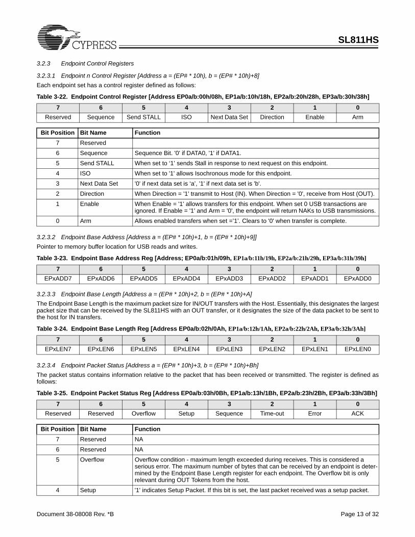
3.2.3 Endpoint Control Registers
3.2.3.1 Endpoint n Control Register [Address a = (EP# * 10h), b = (EP# * 10h)+8]Each endpoint set has a control register defined as follows:
3.2.3.2 Endpoint Base Address [Address a = (EP# * 10h)+1, b = (EP# * 10h)+9]]Pointer to memory buffer location for USB reads and writes.
3.2.3.3 Endpoint Base Length [Address a = (EP# * 10h)+2, b = (EP# * 10h)+A]The Endpoint Base Length is the maximum packet size for IN/OUT transfers with the Host. Essentially, this designates the largestpacket size that can be received by the SL811HS with an OUT transfer, or it designates the size of the data packet to be sent tothe host for IN transfers.
3.2.3.4 Endpoint Packet Status [Address a = (EP# * 10h)+3, b = (EP# * 10h)+Bh]The packet status contains information relative to the packet that has been received or transmitted. The register is defined asfollows:
Table 3-22. Endpoint Control Register [Address EP0a/b:00h/08h, EP1a/b:10h/18h, EP2a/b:20h/28h, EP3a/b:30h/38h]
7 6 5 4 3 2 1 0Reserved Sequence Send STALL ISO Next Data Set Direction Enable Arm
Bit Position Bit Name Function7 Reserved
6 Sequence Sequence Bit. '0' if DATA0, '1' if DATA1.
5 Send STALL When set to ‘1’ sends Stall in response to next request on this endpoint.
4 ISO When set to '1' allows Isochronous mode for this endpoint.
3 Next Data Set '0' if next data set is ‘a’, '1' if next data set is 'b'.
2 Direction When Direction = '1' transmit to Host (IN). When Direction = '0', receive from Host (OUT).
1 Enable When Enable = '1' allows transfers for this endpoint. When set 0 USB transactions are ignored. If Enable = '1' and Arm = '0', the endpoint will return NAKs to USB transmissions.
0 Arm Allows enabled transfers when set =’1’. Clears to '0' when transfer is complete.
Table 3-23. Endpoint Base Address Reg [Address; EP0a/b:01h/09h, EP1a/b:11h/19h, EP2a/b:21h/29h, EP3a/b:31h/39h]
7 6 5 4 3 2 1 0EPxADD7 EPxADD6 EPxADD5 EPxADD4 EPxADD3 EPxADD2 EPxADD1 EPxADD0
Table 3-24. Endpoint Base Length Reg [Address EP0a/b:02h/0Ah, EP1a/b:12h/1Ah, EP2a/b:22h/2Ah, EP3a/b:32h/3Ah]
7 6 5 4 3 2 1 0EPxLEN7 EPxLEN6 EPxLEN5 EPxLEN4 EPxLEN3 EPxLEN2 EPxLEN1 EPxLEN0
Table 3-25. Endpoint Packet Status Reg [Address EP0a/b:03h/0Bh, EP1a/b:13h/1Bh, EP2a/b:23h/2Bh, EP3a/b:33h/3Bh]
7 6 5 4 3 2 1 0Reserved Reserved Overflow Setup Sequence Time-out Error ACK
Bit Position Bit Name Function7 Reserved NA
6 Reserved NA
5 Overflow Overflow condition - maximum length exceeded during receives. This is considered a serious error. The maximum number of bytes that can be received by an endpoint is deter-mined by the Endpoint Base Length register for each endpoint. The Overflow bit is only relevant during OUT Tokens from the host.
4 Setup '1' indicates Setup Packet. If this bit is set, the last packet received was a setup packet.
SL811HS
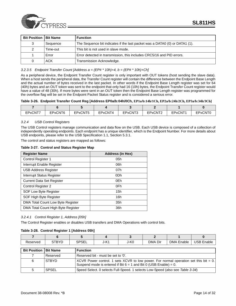
Document 38-08008 Rev. *B Page 14 of 32
3.2.3.5 Endpoint Transfer Count [Address a = (EP# * 10h)+4, b = (EP# * 10h)+Ch]As a peripheral device, the Endpoint Transfer Count register is only important with OUT tokens (host sending the slave data).When a host sends the peripheral data, the Transfer Count register will contain the difference between the Endpoint Base Lengthand the actual number of bytes received in the last packet. In other words if the Endpoint Base Length register was set for 64(40h) bytes and an OUT token was sent to the endpoint that only had 16 (10h) bytes, the Endpoint Transfer Count register wouldhave a value of 48 (30h). If more bytes were sent in an OUT token then the Endpoint Base Length register was programmed forthe overflow flag will be set in the Endpoint Packet Status register and is considered a serious error.
3.2.4 USB Control Registers The USB Control registers manage communication and data flow on the USB. Each USB device is composed of a collection ofindependently operating endpoints. Each endpoint has a unique identifier, which is the Endpoint Number. For more details aboutUSB endpoints, please refer to the USB Specification 1.1, Section 5.3.1.The control and status registers are mapped as follows:
3.2.4.1 Control Register 1, Address [05h]The Control Register enables or disables USB transfers and DMA Operations with control bits.
3 Sequence The Sequence bit indicates if the last packet was a DATA0 (0) or DATA1 (1).
2 Time-out This bit is not used in slave mode.
1 Error Error detected in transmission, this includes CRC5/16 and PID errors.
0 ACK Transmission Acknowledge.
Table 3-26. Endpoint Transfer Count Reg [Address EP0a/b:04h/0Ch, EP1a/b:14h/1Ch, EP2a/b:24h/2Ch, EP3a/b:34h/3Ch]
7 6 5 4 3 2 1 0EPxCNT7 EPxCNT6 EPxCNT5 EPxCNT4 EPxCNT3 EPxCNT2 EPxCNT1 EPxCNT0
Bit Position Bit Name Function
Table 3-27. Control and Status Register Map
Register Name Address (in Hex)Control Register 1 05hInterrupt Enable Register 06hUSB Address Register 07hInterrupt Status Register 0DhCurrent Data Set Register 0EhControl Register 2 0FhSOF Low Byte Register 15hSOF High Byte Register 16hDMA Total Count Low Byte Register 35hDMA Total Count High Byte Register 36h
Table 3-28. Control Register 1 [Address 05h]
7 6 5 4 3 2 1 0Reserved STBYD SPSEL J-K1 J-K0 DMA Dir DMA Enable USB Enable
Bit Position Bit Name Function7 Reserved Reserved bit - must be set to '0'.6 STBYD XCVR Power control. 1 sets XCVR to low power. For normal operation set this bit = 0.
Suspend mode is entered if Bit 6 = 1 and Bit 0 (USB Enable) = 0. 5 SPSEL Speed Select. 0 selects Full-Speed. 1 selects Low-Speed (also see Table 3-34)
SL811HS
Document 38-08008 Rev. *B Page 15 of 32
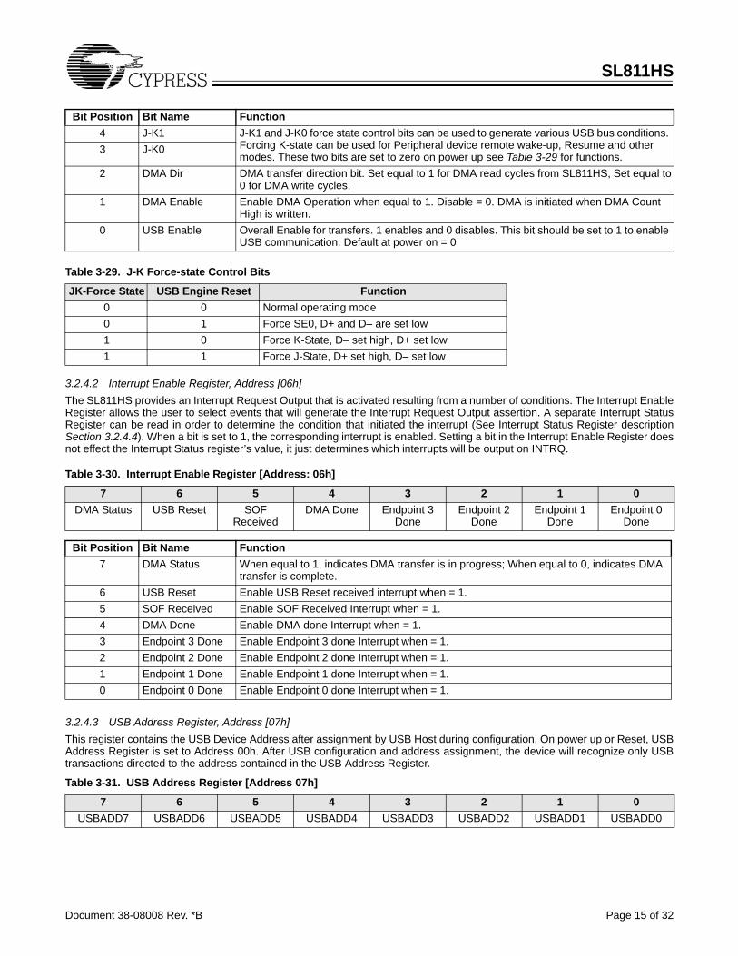
3.2.4.2 Interrupt Enable Register, Address [06h] The SL811HS provides an Interrupt Request Output that is activated resulting from a number of conditions. The Interrupt EnableRegister allows the user to select events that will generate the Interrupt Request Output assertion. A separate Interrupt StatusRegister can be read in order to determine the condition that initiated the interrupt (See Interrupt Status Register descriptionSection 3.2.4.4). When a bit is set to 1, the corresponding interrupt is enabled. Setting a bit in the Interrupt Enable Register doesnot effect the Interrupt Status register’s value, it just determines which interrupts will be output on INTRQ.
3.2.4.3 USB Address Register, Address [07h]This register contains the USB Device Address after assignment by USB Host during configuration. On power up or Reset, USBAddress Register is set to Address 00h. After USB configuration and address assignment, the device will recognize only USBtransactions directed to the address contained in the USB Address Register.
4 J-K1 J-K1 and J-K0 force state control bits can be used to generate various USB bus conditions. Forcing K-state can be used for Peripheral device remote wake-up, Resume and other modes. These two bits are set to zero on power up see Table 3-29 for functions.
3 J-K0
2 DMA Dir DMA transfer direction bit. Set equal to 1 for DMA read cycles from SL811HS, Set equal to0 for DMA write cycles.
1 DMA Enable Enable DMA Operation when equal to 1. Disable = 0. DMA is initiated when DMA Count High is written.
0 USB Enable Overall Enable for transfers. 1 enables and 0 disables. This bit should be set to 1 to enable USB communication. Default at power on = 0
Bit Position Bit Name Function
Table 3-29. J-K Force-state Control Bits
JK-Force State USB Engine Reset Function0 0 Normal operating mode0 1 Force SE0, D+ and D– are set low1 0 Force K-State, D– set high, D+ set low1 1 Force J-State, D+ set high, D– set low
Table 3-30. Interrupt Enable Register [Address: 06h]
7 6 5 4 3 2 1 0DMA Status USB Reset SOF
ReceivedDMA Done Endpoint 3
DoneEndpoint 2
DoneEndpoint 1
DoneEndpoint 0
Done
Bit Position Bit Name Function7 DMA Status When equal to 1, indicates DMA transfer is in progress; When equal to 0, indicates DMA
transfer is complete.6 USB Reset Enable USB Reset received interrupt when = 1.5 SOF Received Enable SOF Received Interrupt when = 1.4 DMA Done Enable DMA done Interrupt when = 1.3 Endpoint 3 Done Enable Endpoint 3 done Interrupt when = 1.2 Endpoint 2 Done Enable Endpoint 2 done Interrupt when = 1.1 Endpoint 1 Done Enable Endpoint 1 done Interrupt when = 1.0 Endpoint 0 Done Enable Endpoint 0 done Interrupt when = 1.
Table 3-31. USB Address Register [Address 07h]
7 6 5 4 3 2 1 0USBADD7 USBADD6 USBADD5 USBADD4 USBADD3 USBADD2 USBADD1 USBADD0
SL811HS
Document 38-08008 Rev. *B Page 16 of 32
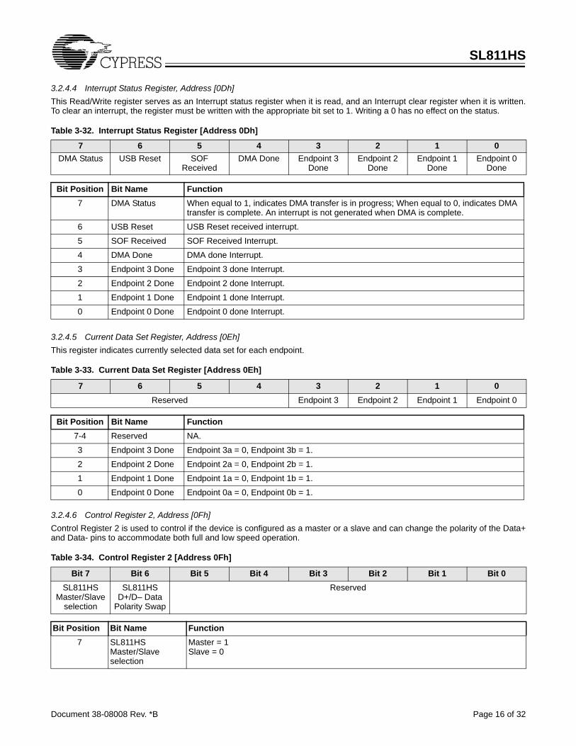
3.2.4.4 Interrupt Status Register, Address [0Dh]This Read/Write register serves as an Interrupt status register when it is read, and an Interrupt clear register when it is written.To clear an interrupt, the register must be written with the appropriate bit set to 1. Writing a 0 has no effect on the status.
3.2.4.5 Current Data Set Register, Address [0Eh]This register indicates currently selected data set for each endpoint.
3.2.4.6 Control Register 2, Address [0Fh]Control Register 2 is used to control if the device is configured as a master or a slave and can change the polarity of the Data+and Data- pins to accommodate both full and low speed operation.
Table 3-32. Interrupt Status Register [Address 0Dh]
7 6 5 4 3 2 1 0DMA Status USB Reset SOF
ReceivedDMA Done Endpoint 3
DoneEndpoint 2
DoneEndpoint 1
DoneEndpoint 0
Done
Bit Position Bit Name Function7 DMA Status When equal to 1, indicates DMA transfer is in progress; When equal to 0, indicates DMA
transfer is complete. An interrupt is not generated when DMA is complete.
6 USB Reset USB Reset received interrupt.
5 SOF Received SOF Received Interrupt.
4 DMA Done DMA done Interrupt.
3 Endpoint 3 Done Endpoint 3 done Interrupt.
2 Endpoint 2 Done Endpoint 2 done Interrupt.
1 Endpoint 1 Done Endpoint 1 done Interrupt.
0 Endpoint 0 Done Endpoint 0 done Interrupt.
Table 3-33. Current Data Set Register [Address 0Eh]
7 6 5 4 3 2 1 0Reserved Endpoint 3 Endpoint 2 Endpoint 1 Endpoint 0
Bit Position Bit Name Function7-4 Reserved NA.
3 Endpoint 3 Done Endpoint 3a = 0, Endpoint 3b = 1.
2 Endpoint 2 Done Endpoint 2a = 0, Endpoint 2b = 1.
1 Endpoint 1 Done Endpoint 1a = 0, Endpoint 1b = 1.
0 Endpoint 0 Done Endpoint 0a = 0, Endpoint 0b = 1.
Table 3-34. Control Register 2 [Address 0Fh]
Bit 7 Bit 6 Bit 5 Bit 4 Bit 3 Bit 2 Bit 1 Bit 0SL811HS
Master/Slave selection
SL811HS D+/D– Data
Polarity Swap
Reserved
Bit Position Bit Name Function7 SL811HS
Master/Slave selection
Master = 1Slave = 0
SL811HS
Document 38-08008 Rev. *B Page 17 of 32
3.2.4.7 SOF Low Register, Address [15h]Read only Register contains the 7 low order bits of FrameNumber in positions: bit 7:1. Bit 0 is undefined. Register isupdated when a SOF packet is received. User should not writeto this register.
3.2.4.8 SOF High Register, Address [16h]Read only Register contains the 4 low order bits of FrameNumber in positions: bit 7:4. Bits 3:0 are undefined, and shouldbe masked when read by the user. This register is updatedwhen a SOF packet is received. The user should not write tothis register.
3.2.4.9 DMA Total Count Low Register, Address [35h]The DMA Total Count Low Register contains the low order 8-bits of DMA count. DMA total count is the total number of bytesto be transferred between a peripheral to the SL811HS. Thecount may sometimes require up to 16-bits, thus the count isrepresented in two registers: Total Count Low, and Total CountHigh. EP3 is only supported with DMA operation.
3.2.4.10 DMA Total Count High Register, Address [36h]The DMA Total Count High Register contains the High order8-bits of DMA count. When written, this register enables DMAif the DMA Enable bit is set in the Control Register 1. The usershould always write Low Count Register first, followed by awrite to High Count Register, even if high count is 00h.
6 SL811HS D+/D– Data Polarity Swap
“1” = change polarity (low-speed)“0” = no change of polarity (full-speed)
5-0 Reserved NA
Bit Position Bit Name Function
SL811HS
Document 38-08008 Rev. *B Page 18 of 32
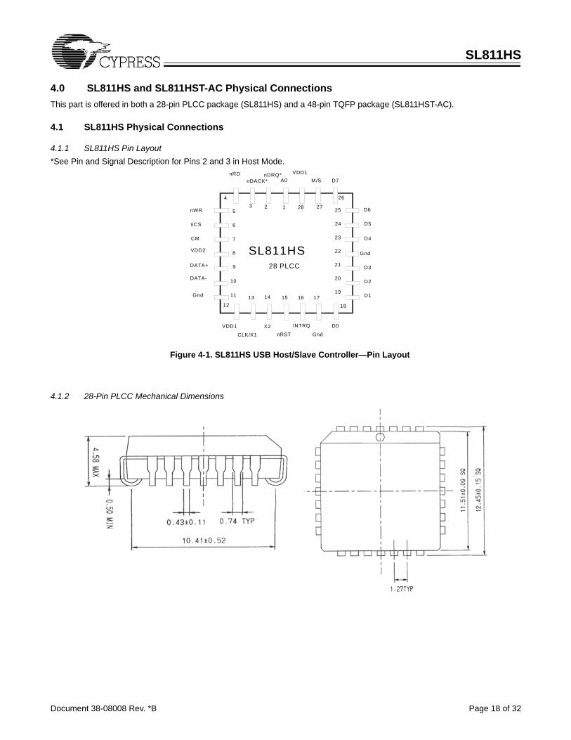
4.0 SL811HS and SL811HST-AC Physical ConnectionsThis part is offered in both a 28-pin PLCC package (SL811HS) and a 48-pin TQFP package (SL811HST-AC).
4.1 SL811HS Physical Connections
4.1.1 SL811HS Pin Layout*See Pin and Signal Description for Pins 2 and 3 in Host Mode.
4.1.2 28-Pin PLCC Mechanical Dimensions
12 28
nDRQ*nDACK*
nRD
nWR
D7
D6
D5
D4
Gnd
D3
D2
D1
D0
Gnd
INTRQ
VDD1
nRST
VDD2
Gnd
nCS
DATA-
DATA+
VDD1
CLK/X1
X2
SL811HS 28 PLCC
A0 M/S
171615141312
11
10
9
8
7
6
5
4 3
25
24
22
21
20
19
18
27
26
23CM
Figure 4-1. SL811HS USB Host/Slave Controller—Pin Layout
SL811HS
Document 38-08008 Rev. *B Page 19 of 32
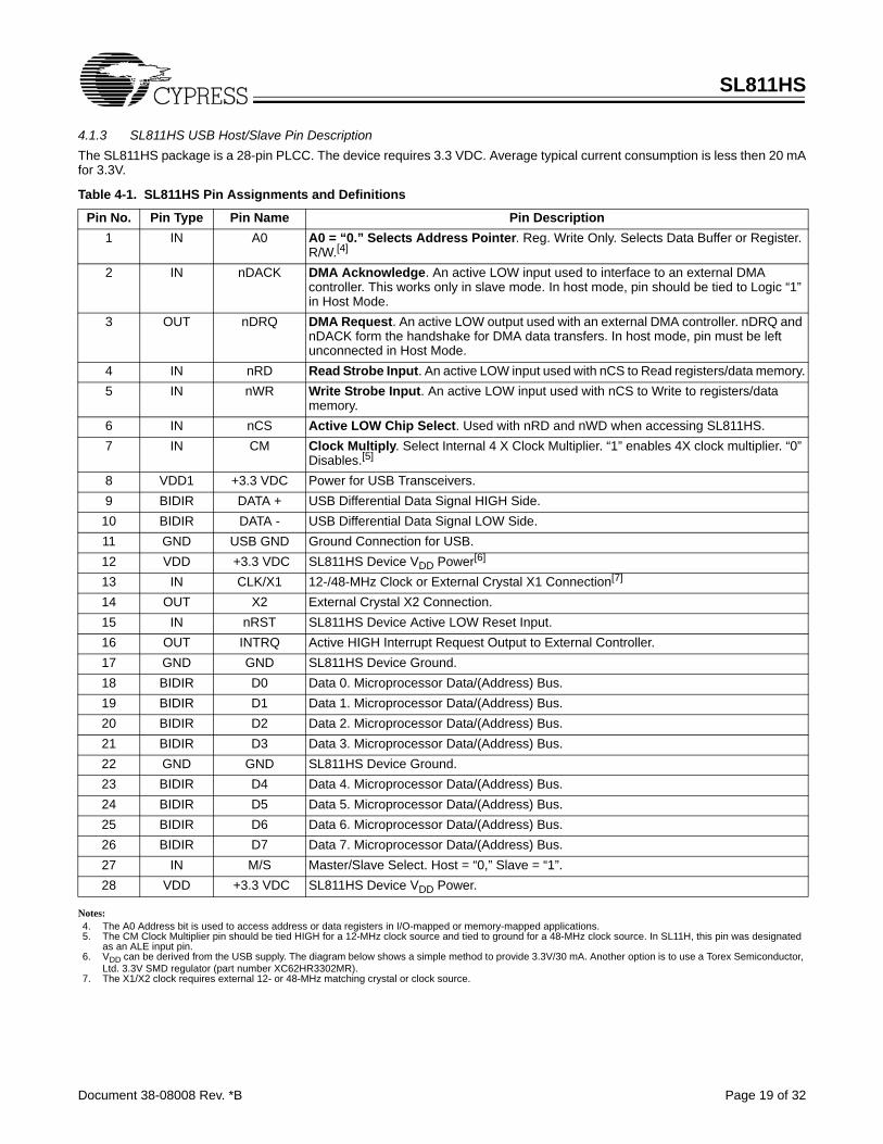
4.1.3 SL811HS USB Host/Slave Pin DescriptionThe SL811HS package is a 28-pin PLCC. The device requires 3.3 VDC. Average typical current consumption is less then 20 mAfor 3.3V.
Notes:4. The A0 Address bit is used to access address or data registers in I/O-mapped or memory-mapped applications. 5. The CM Clock Multiplier pin should be tied HIGH for a 12-MHz clock source and tied to ground for a 48-MHz clock source. In SL11H, this pin was designated
as an ALE input pin.6. VDD can be derived from the USB supply. The diagram below shows a simple method to provide 3.3V/30 mA. Another option is to use a Torex Semiconductor,
Ltd. 3.3V SMD regulator (part number XC62HR3302MR).7. The X1/X2 clock requires external 12- or 48-MHz matching crystal or clock source.
Table 4-1. SL811HS Pin Assignments and Definitions
Pin No. Pin Type Pin Name Pin Description1 IN A0 A0 = “0.” Selects Address Pointer. Reg. Write Only. Selects Data Buffer or Register.
R/W.[4]
2 IN nDACK DMA Acknowledge. An active LOW input used to interface to an external DMA controller. This works only in slave mode. In host mode, pin should be tied to Logic “1” in Host Mode.
3 OUT nDRQ DMA Request. An active LOW output used with an external DMA controller. nDRQ and nDACK form the handshake for DMA data transfers. In host mode, pin must be left unconnected in Host Mode.
4 IN nRD Read Strobe Input. An active LOW input used with nCS to Read registers/data memory.5 IN nWR Write Strobe Input. An active LOW input used with nCS to Write to registers/data
memory. 6 IN nCS Active LOW Chip Select. Used with nRD and nWD when accessing SL811HS. 7 IN CM Clock Multiply. Select Internal 4 X Clock Multiplier. “1” enables 4X clock multiplier. “0”
Disables.[5]
8 VDD1 +3.3 VDC Power for USB Transceivers.9 BIDIR DATA + USB Differential Data Signal HIGH Side.
10 BIDIR DATA - USB Differential Data Signal LOW Side.11 GND USB GND Ground Connection for USB.12 VDD +3.3 VDC SL811HS Device VDD Power[6]
13 IN CLK/X1 12-/48-MHz Clock or External Crystal X1 Connection[7]
14 OUT X2 External Crystal X2 Connection.15 IN nRST SL811HS Device Active LOW Reset Input.16 OUT INTRQ Active HIGH Interrupt Request Output to External Controller.17 GND GND SL811HS Device Ground.18 BIDIR D0 Data 0. Microprocessor Data/(Address) Bus.19 BIDIR D1 Data 1. Microprocessor Data/(Address) Bus.20 BIDIR D2 Data 2. Microprocessor Data/(Address) Bus.21 BIDIR D3 Data 3. Microprocessor Data/(Address) Bus.22 GND GND SL811HS Device Ground.23 BIDIR D4 Data 4. Microprocessor Data/(Address) Bus.24 BIDIR D5 Data 5. Microprocessor Data/(Address) Bus.25 BIDIR D6 Data 6. Microprocessor Data/(Address) Bus.26 BIDIR D7 Data 7. Microprocessor Data/(Address) Bus.27 IN M/S Master/Slave Select. Host = “0,” Slave = “1”.28 VDD +3.3 VDC SL811HS Device VDD Power.
SL811HS
Document 38-08008 Rev. *B Page 20 of 32
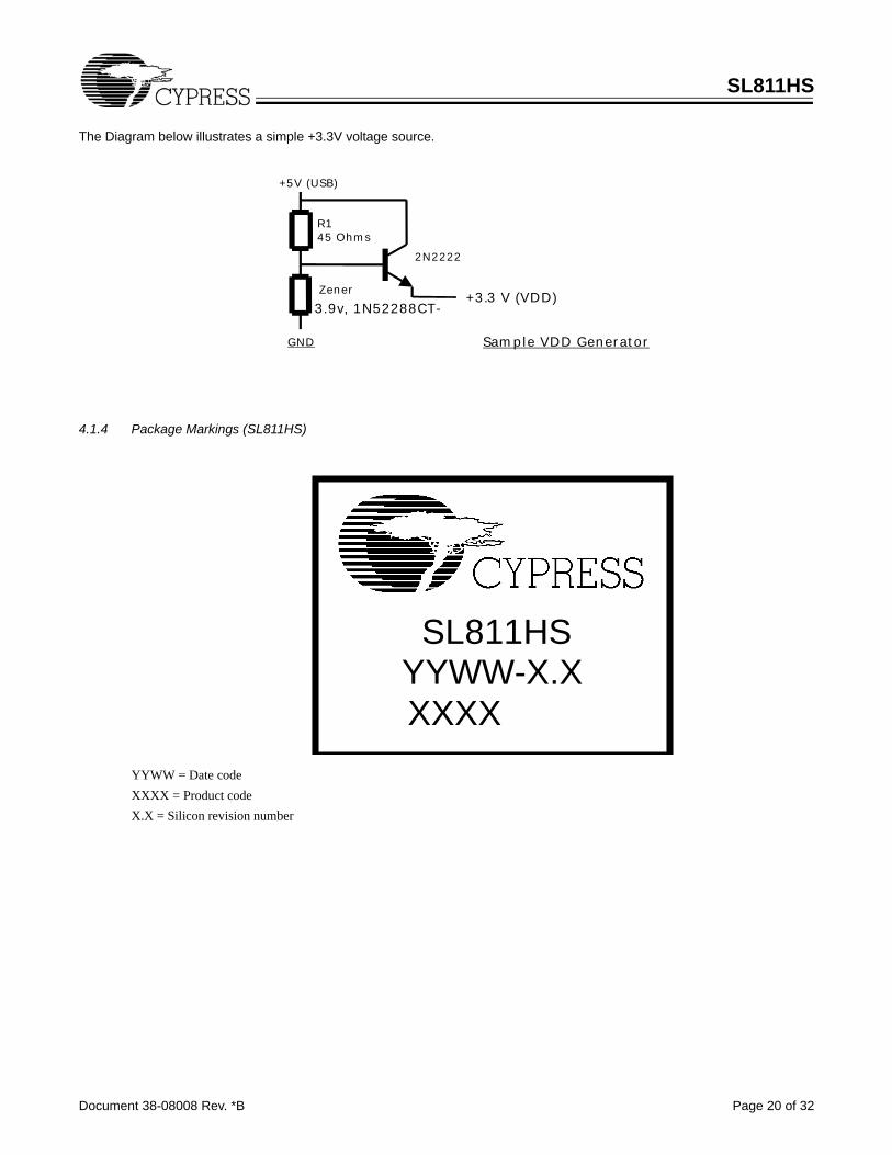
The Diagram below illustrates a simple +3.3V voltage source.
4.1.4 Package Markings (SL811HS)
YYWW = Date codeXXXX = Product codeX.X = Silicon revision number
+5V (USB)
GND
R1
+3.3 V (VDD)
Sample VDD Generator
45 Ohms
3.9v, 1N52288CT-Zener
2N2222
SL811HSYYWW-X.X
XXXX
SL811HS
Document 38-08008 Rev. *B Page 21 of 32
4.2 SL811HST-AC Physical Connections
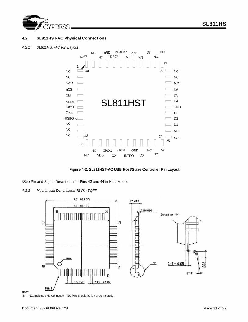
4.2.1 SL811HST-AC Pin Layout
*See Pin and Signal Description for Pins 43 and 44 in Host Mode.
4.2.2 Mechanical Dimensions 48-Pin TQFP
Note:8. NC. Indicates No Connection. NC Pins should be left unconnected.
SL811HST
1
12
13
2425
48
37
36
NC
NC NC
NC
NC
NCNC
NCNC NC
Data-
nRD NC
NC NC
NC
NC
nWR
nCS
CM
VDD1Data+
VDD Clk/X1
X2
nRST
INTRQ GND
D0
D1
D2
D3
GND
D4
D5
D6
D7VDDM/SA0
nDACK*NC[8] nDRQ*
USBGnd NC
NC
NC
NC
Figure 4-2. SL811HST-AC USB Host/Slave Controller Pin Layout
SL811HS
Document 38-08008 Rev. *B Page 22 of 32
4.2.3 SL811HST-AC USB Host Controller Pins DescriptionThe SL811HST-AC is packaged in a 48-pin TQFP. The device requires a 3.3VDC power source. The SL811HST-AC requires anexternal 12 or 48 MHz crystal or Clock.
Table 4-2. SL811HST-AC Pin Assignments and Definitions
Pin No. Pin Type Pin Name Pin Description1 NC NC NC2 NC NC NC3 IN nWR Write Strobe Input. An active LOW input used with nCS to Write to
registers/data memory. 4 IN nCS Active LOW SL811HST-AC Chip select. Used with nRD and nWr when
accessing SL811HT. 5 IN CM Clock Multiply. Select 12-MHz/48-MHz Clock Source.[9]
6 VDD1 +3.3 VDC Power for USB Transceivers. VDD1 may be connected to VDD.7 BIDIR DATA + USB Differential Data Signal HIGH Side.8 BIDIR DATA - USB Differential Data Signal LOW Side.9 GND USB GND Ground Connection for USB.10 NC NC NC11 NC NC NC12 NC NC NC13 NC NC NC14 NC NC NC15 VDD +3.3 VDC SL811HST-AC Device VDD Power.[10]
16 IN CLK/X1 Clock or External Crystal X1 connection.[11]
17 OUT X2 External Crystal X2 connection.18 IN nRST SL811HST-AC Device active low reset input.19 OUT INTRQ Active HIGH Interrupt Request output to external controller.20 GND GND SL811HST-AC Device Ground.21 BIDIR D0 Data 0. Microprocessor Data/(Address) Bus.22 NC NC NC23 NC NC NC24 NC NC NC25 NC NC NC26 NC NC NC27 BIDIR D1 Data 1. Microprocessor Data/(Address) Bus.28 BIDIR D2 Data 2. Microprocessor Data/(Address) Bus.29 BIDIR D3 Data 3. Microprocessor Data/(Address) Bus.30 GND GND SL811HST-AC Device Ground.31 BIDIR D4 Data 4. Microprocessor Data/(Address) Bus.32 BIDIR D5 Data 5. Microprocessor Data/(Address) Bus.
Notes:9. The CM Clock Multiplier pin should be tied HIGH for a 12-MHz clock source and tied to ground for a 48-MHz clock source. In SL11H, this pin was designated
as ALE input pin.10. VDD can be derived from the USB supply. See diagram.11. The X1/X2 Clock requires external 12- or 48-MHz matching crystal or clock source.
SL811HS
Document 38-08008 Rev. *B Page 23 of 32
Notes:12. The A0 Address bit is used to access address register or data registers in I/O Mapped or Memory Mapped applications.
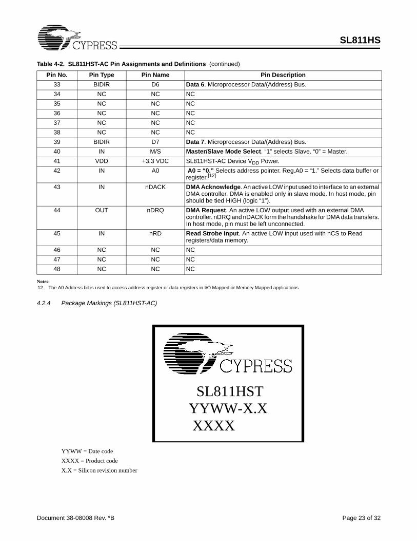
4.2.4 Package Markings (SL811HST-AC)
YYWW = Date codeXXXX = Product codeX.X = Silicon revision number
33 BIDIR D6 Data 6. Microprocessor Data/(Address) Bus.34 NC NC NC35 NC NC NC36 NC NC NC37 NC NC NC38 NC NC NC39 BIDIR D7 Data 7. Microprocessor Data/(Address) Bus. 40 IN M/S Master/Slave Mode Select. “1” selects Slave. “0” = Master.41 VDD +3.3 VDC SL811HST-AC Device VDD Power.42 IN A0 A0 = “0.” Selects address pointer. Reg.A0 = “1.” Selects data buffer or
register.[12]
43 IN nDACK DMA Acknowledge. An active LOW input used to interface to an external DMA controller. DMA is enabled only in slave mode. In host mode, pin should be tied HIGH (logic “1”).
44 OUT nDRQ DMA Request. An active LOW output used with an external DMA controller. nDRQ and nDACK form the handshake for DMA data transfers. In host mode, pin must be left unconnected.
45 IN nRD Read Strobe Input. An active LOW input used with nCS to Read registers/data memory.
46 NC NC NC47 NC NC NC48 NC NC NC
Table 4-2. SL811HST-AC Pin Assignments and Definitions (continued)
Pin No. Pin Type Pin Name Pin Description
SL811HSTYYWW-X.X
XXXX
SL811HS
Document 38-08008 Rev. *B Page 24 of 32
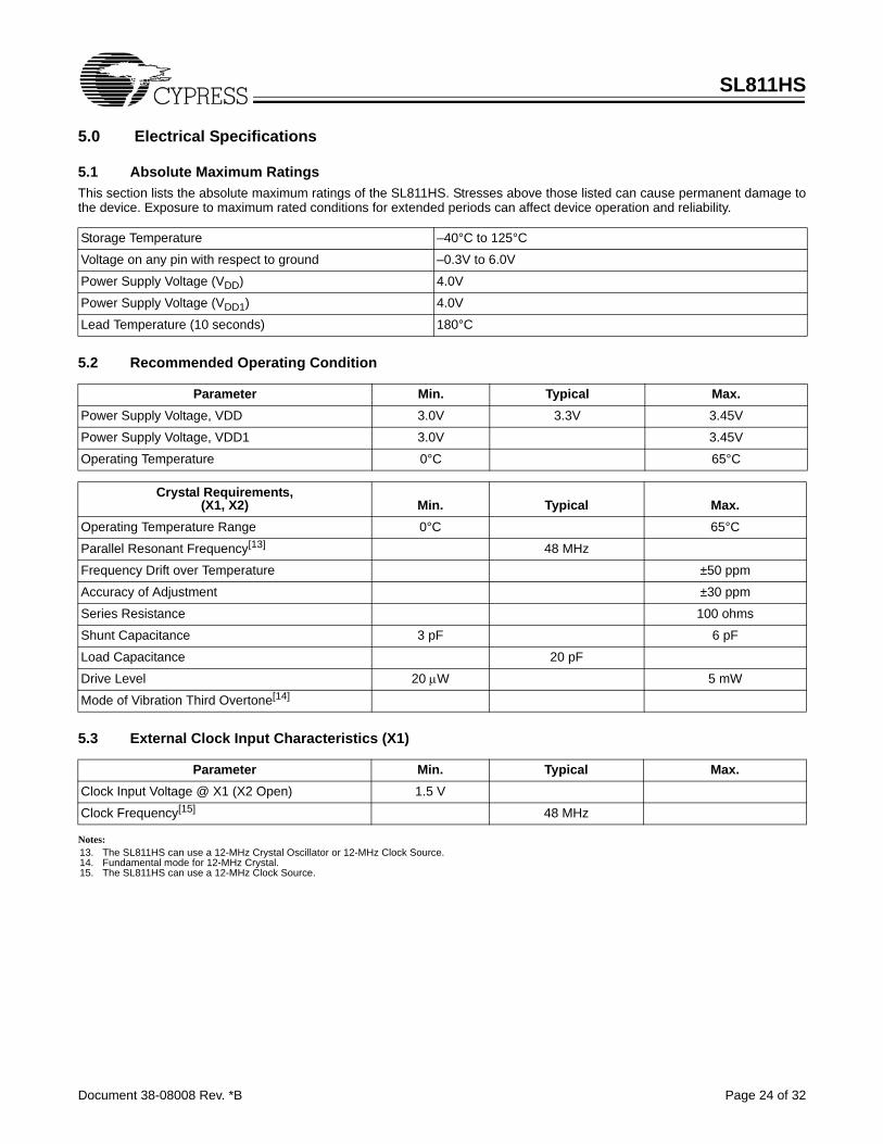
5.0 Electrical Specifications
5.1 Absolute Maximum RatingsThis section lists the absolute maximum ratings of the SL811HS. Stresses above those listed can cause permanent damage tothe device. Exposure to maximum rated conditions for extended periods can affect device operation and reliability.
5.2 Recommended Operating Condition
5.3 External Clock Input Characteristics (X1)
Notes:13. The SL811HS can use a 12-MHz Crystal Oscillator or 12-MHz Clock Source.14. Fundamental mode for 12-MHz Crystal.15. The SL811HS can use a 12-MHz Clock Source.
Storage Temperature –40°C to 125°C
Voltage on any pin with respect to ground –0.3V to 6.0V
Power Supply Voltage (VDD) 4.0V
Power Supply Voltage (VDD1) 4.0V
Lead Temperature (10 seconds) 180°C
Parameter Min. Typical Max.Power Supply Voltage, VDD 3.0V 3.3V 3.45V
Power Supply Voltage, VDD1 3.0V 3.45V
Operating Temperature 0°C 65°C
Crystal Requirements,(X1, X2) Min. Typical Max.
Operating Temperature Range 0°C 65°C
Parallel Resonant Frequency[13] 48 MHz
Frequency Drift over Temperature ±50 ppm
Accuracy of Adjustment ±30 ppm
Series Resistance 100 ohms
Shunt Capacitance 3 pF 6 pF
Load Capacitance 20 pF
Drive Level 20 µW 5 mW
Mode of Vibration Third Overtone[14]
Parameter Min. Typical Max.Clock Input Voltage @ X1 (X2 Open) 1.5 V
Clock Frequency[15] 48 MHz
SL811HS
Document 38-08008 Rev. *B Page 25 of 32
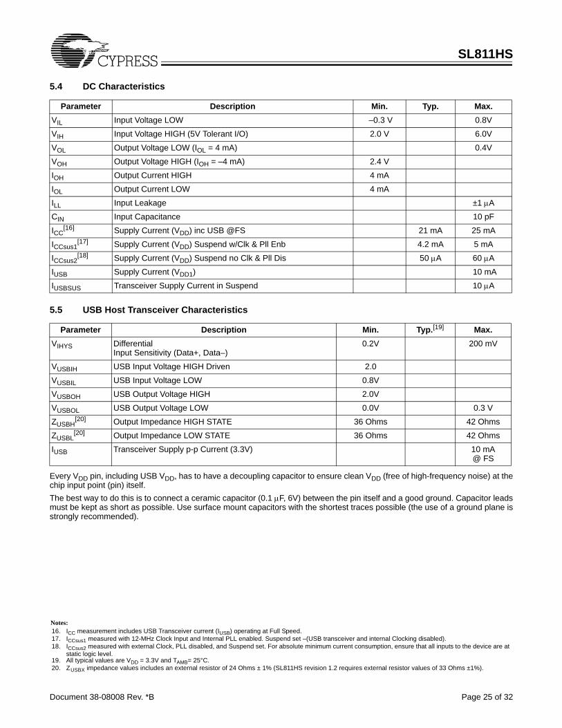
5.4 DC Characteristics
5.5 USB Host Transceiver Characteristics
Every VDD pin, including USB VDD, has to have a decoupling capacitor to ensure clean VDD (free of high-frequency noise) at thechip input point (pin) itself.The best way to do this is to connect a ceramic capacitor (0.1 µF, 6V) between the pin itself and a good ground. Capacitor leadsmust be kept as short as possible. Use surface mount capacitors with the shortest traces possible (the use of a ground plane isstrongly recommended).
Parameter Description Min. Typ. Max.VIL Input Voltage LOW –0.3 V 0.8V
VIH Input Voltage HIGH (5V Tolerant I/O) 2.0 V 6.0V
VOL Output Voltage LOW (IOL = 4 mA) 0.4V
VOH Output Voltage HIGH (IOH = –4 mA) 2.4 V
IOH Output Current HIGH 4 mA
IOL Output Current LOW 4 mA
ILL Input Leakage ±1 µA
CIN Input Capacitance 10 pF
ICC[16] Supply Current (VDD) inc USB @FS 21 mA 25 mA
ICCsus1[17] Supply Current (VDD) Suspend w/Clk & Pll Enb 4.2 mA 5 mA
ICCsus2[18] Supply Current (VDD) Suspend no Clk & Pll Dis 50 µA 60 µA
IUSB Supply Current (VDD1) 10 mA
IUSBSUS Transceiver Supply Current in Suspend 10 µA
Parameter Description Min. Typ.[19] Max.VIHYS Differential
Input Sensitivity (Data+, Data–)0.2V 200 mV
VUSBIH USB Input Voltage HIGH Driven 2.0
VUSBIL USB Input Voltage LOW 0.8V
VUSBOH USB Output Voltage HIGH 2.0V
VUSBOL USB Output Voltage LOW 0.0V 0.3 V
ZUSBH[20] Output Impedance HIGH STATE 36 Ohms 42 Ohms
ZUSBL[20] Output Impedance LOW STATE 36 Ohms 42 Ohms
IUSB Transceiver Supply p-p Current (3.3V) 10 mA@ FS
Notes:16. ICC measurement includes USB Transceiver current (IUSB) operating at Full Speed. 17. ICCsus1 measured with 12-MHz Clock Input and Internal PLL enabled. Suspend set –(USB transceiver and internal Clocking disabled).18. ICCsus2 measured with external Clock, PLL disabled, and Suspend set. For absolute minimum current consumption, ensure that all inputs to the device are at
static logic level.19. All typical values are VDD = 3.3V and TAMB= 25°C.20. ZUSBX impedance values includes an external resistor of 24 Ohms ± 1% (SL811HS revision 1.2 requires external resistor values of 33 Ohms ±1%).
SL811HS
Document 38-08008 Rev. *B Page 26 of 32
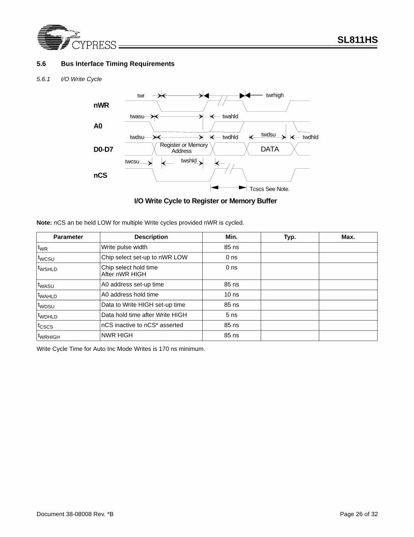
5.6 Bus Interface Timing Requirements
5.6.1 I/O Write Cycle
Note: nCS an be held LOW for multiple Write cycles provided nWR is cycled.
Write Cycle Time for Auto Inc Mode Writes is 170 ns minimum.
Parameter Description Min. Typ. Max.tWR Write pulse width 85 ns
tWCSU Chip select set-up to nWR LOW 0 ns
tWSHLD Chip select hold timeAfter nWR HIGH
0 ns
tWASU A0 address set-up time 85 ns
tWAHLD A0 address hold time 10 ns
tWDSU Data to Write HIGH set-up time 85 ns
tWDHLD Data hold time after Write HIGH 5 ns
tCSCS nCS inactive to nCS* asserted 85 ns
tWRHIGH NWR HIGH 85 ns
nWR
A0
D0-D7 DATA
twr
twahld
twdhld
twasu
twdsu twdsu twdhld
I/O Write Cycle to Register or Memory Buffer
Register or MemoryAddress
nCS
twcsu twshld
Tcscs See Note.
twrhigh
SL811HS
Document 38-08008 Rev. *B Page 27 of 32
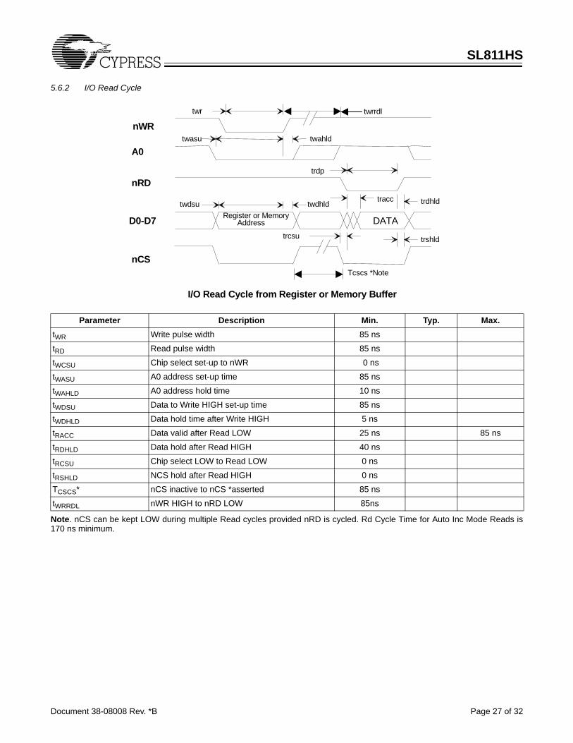
5.6.2 I/O Read Cycle
Note. nCS can be kept LOW during multiple Read cycles provided nRD is cycled. Rd Cycle Time for Auto Inc Mode Reads is170 ns minimum.
nRD
A0
D0-D7 DATA
twr
twahld
twdhld
twasu
twdsu trdhld
I/O Read Cycle from Register or Memory Buffer
Register or MemoryAddress
trdp
nWR
trshld trcsu
nCS
tracc
Tcscs *Note
twrrdl
Parameter Description Min. Typ. Max.tWR Write pulse width 85 ns
tRD Read pulse width 85 ns
tWCSU Chip select set-up to nWR 0 ns
tWASU A0 address set-up time 85 ns
tWAHLD A0 address hold time 10 ns
tWDSU Data to Write HIGH set-up time 85 ns
tWDHLD Data hold time after Write HIGH 5 ns
tRACC Data valid after Read LOW 25 ns 85 ns
tRDHLD Data hold after Read HIGH 40 ns
tRCSU Chip select LOW to Read LOW 0 ns
tRSHLD NCS hold after Read HIGH 0 ns
TCSCS* nCS inactive to nCS *asserted 85 ns
tWRRDL nWR HIGH to nRD LOW 85ns
SL811HS
Document 38-08008 Rev. *B Page 28 of 32
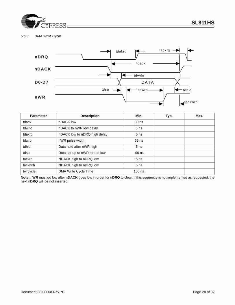
5.6.3 DMA Write Cycle
Note: nWR must go low after nDACK goes low in order for nDRQ to clear. If this sequence is not implemented as requested, thenext nDRQ will be not inserted.
Parameter Description Min. Typ. Max.
tdack nDACK low 80 ns
tdwrlo nDACK to nWR low delay 5 ns
tdakrq nDACK low to nDRQ high delay 5 ns
tdwrp nWR pulse width 65 ns
tdhld Data hold after nWR high 5 ns
tdsu Data set-up to nWR strobe low 60 ns
tackrq NDACK high to nDRQ low 5 ns
tackwrh NDACK high to nDRQ low 5 ns
twrcycle DMA Write Cycle Time 150 ns
nDRQ
nDACK
D0-D7 DATA
nW R
tdwrp tdsu
tdack
tdhld
tdwrlo
tackwrh
tdakrq tackrq
SL811HS
Document 38-08008 Rev. *B Page 29 of 32
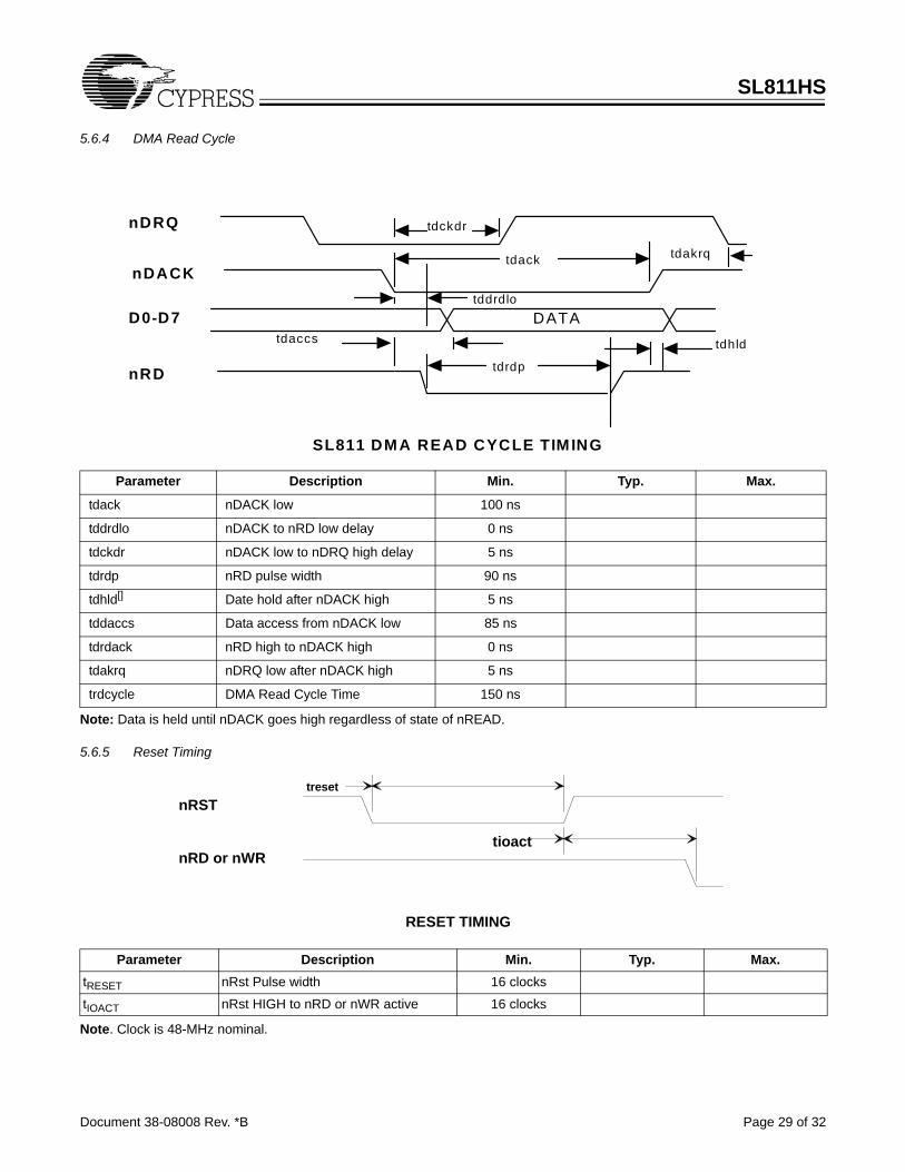
5.6.4 DMA Read Cycle
Note: Data is held until nDACK goes high regardless of state of nREAD.
5.6.5 Reset Timing
Note. Clock is 48-MHz nominal.
Parameter Description Min. Typ. Max.
tdack nDACK low 100 ns
tddrdlo nDACK to nRD low delay 0 ns
tdckdr nDACK low to nDRQ high delay 5 ns
tdrdp nRD pulse width 90 ns
tdhld[] Date hold after nDACK high 5 ns
tddaccs Data access from nDACK low 85 ns
tdrdack nRD high to nDACK high 0 ns
tdakrq nDRQ low after nDACK high 5 ns
trdcycle DMA Read Cycle Time 150 ns
nDRQ
nDACK
D0-D7 DATA
nRD
SL811 DMA READ CYCLE TIM ING
tdrdp
tdaccs
tdack
tdhld
tddrdlo
tdckdr
tdakrq
nRST
nRD or nWR
treset
tioact
RESET TIMING
Parameter Description Min. Typ. Max.tRESET nRst Pulse width 16 clocks
tIOACT nRst HIGH to nRD or nWR active 16 clocks
SL811HS
Document 38-08008 Rev. *B Page 30 of 32
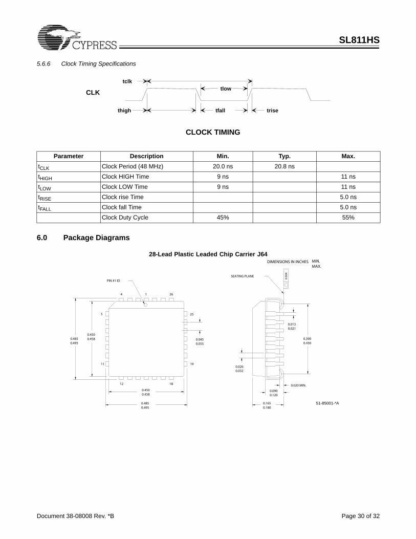
5.6.6 Clock Timing Specifications
6.0 Package Diagrams
CLK
CLOCK TIMING
trisetfallthigh
tclktlow
Parameter Description Min. Typ. Max.tCLK Clock Period (48 MHz) 20.0 ns 20.8 ns
tHIGH Clock HIGH Time 9 ns 11 ns
tLOW Clock LOW Time 9 ns 11 ns
tRISE Clock rise Time 5.0 ns
tFALL Clock fall Time 5.0 ns
Clock Duty Cycle 45% 55%
DIMENSIONS IN INCHES MIN.MAX.
0.0450.055
0.026
0.013
0.032
0.021
0.020 MIN.
0.090
0.165
0.120
0.180
0.4850.495
0.4500.458
0.4580.450
0.4950.485
0.3900.430
4 26
1812
11
5
19
25
0.00
4
SEATING PLANE
1
PIN #1 ID
28-Lead Plastic Leaded Chip Carrier J64
51-85001-*A
SL811HS
Document 38-08008 Rev. *B Page 31 of 32© Cypress Semiconductor Corporation, 2005. The information contained herein is subject to change without notice. Cypress Semiconductor Corporation assumes no responsibility for the useof any circuitry other than circuitry embodied in a Cypress product. Nor does it convey or imply any license under patent or other rights. Cypress products are not warranted nor intended to beused for medical, life support, life saving, critical control or safety applications, unless pursuant to an express written agreement with Cypress. Furthermore, Cypress does not authorize itsproducts for use as critical components in life-support systems where a malfunction or failure may reasonably be expected to result in significant injury to the user. The inclusion of Cypressproducts in life-support systems application implies that the manufacturer assumes all risk of such use and in doing so indemnifies Cypress against all charges.
Intel is a registered trademark of Intel Corporation. Torex is a trademark of Torex Semiconductors, Ltd. SL811HS is a trademarkof Cypress Semiconductor Corporation. All product and company names mentioned in this document may be the trademarks oftheir respective holders.
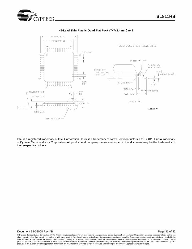
48-Lead Thin Plastic Quad Flat Pack (7x7x1.4 mm) A48
51-85135-**
SL811HS
Document 38-08008 Rev. *B Page 32 of 32
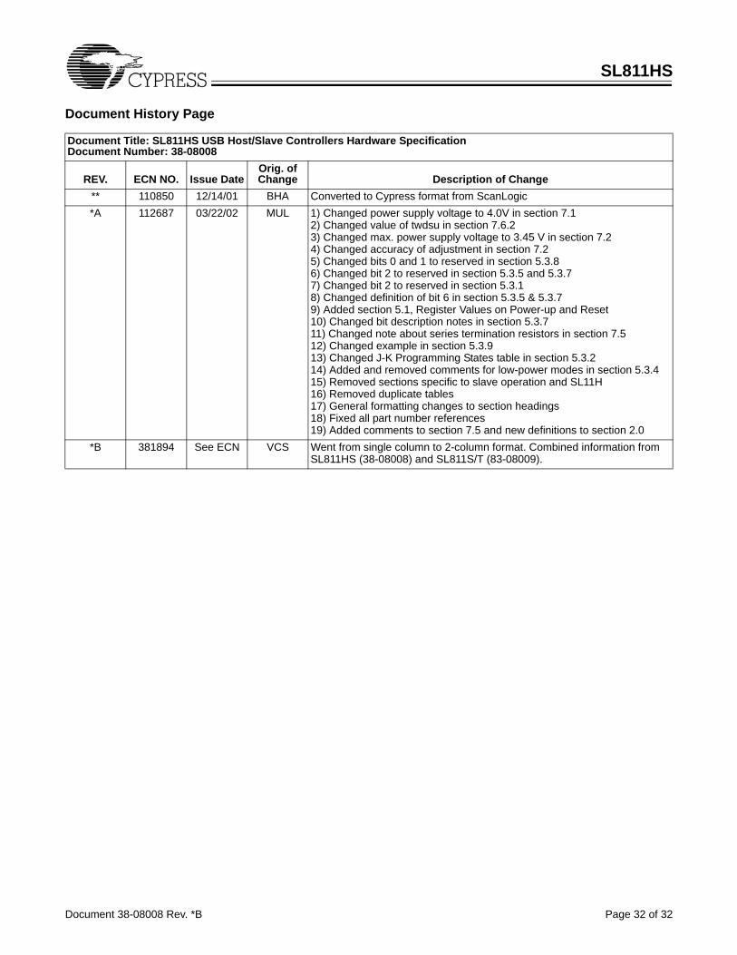
Document History Page
Document Title: SL811HS USB Host/Slave Controllers Hardware SpecificationDocument Number: 38-08008
REV. ECN NO. Issue DateOrig. of Change Description of Change
** 110850 12/14/01 BHA Converted to Cypress format from ScanLogic*A 112687 03/22/02 MUL 1) Changed power supply voltage to 4.0V in section 7.1
2) Changed value of twdsu in section 7.6.23) Changed max. power supply voltage to 3.45 V in section 7.24) Changed accuracy of adjustment in section 7.25) Changed bits 0 and 1 to reserved in section 5.3.86) Changed bit 2 to reserved in section 5.3.5 and 5.3.77) Changed bit 2 to reserved in section 5.3.18) Changed definition of bit 6 in section 5.3.5 & 5.3.79) Added section 5.1, Register Values on Power-up and Reset10) Changed bit description notes in section 5.3.711) Changed note about series termination resistors in section 7.512) Changed example in section 5.3.913) Changed J-K Programming States table in section 5.3.214) Added and removed comments for low-power modes in section 5.3.415) Removed sections specific to slave operation and SL11H16) Removed duplicate tables17) General formatting changes to section headings18) Fixed all part number references19) Added comments to section 7.5 and new definitions to section 2.0
*B 381894 See ECN VCS Went from single column to 2-column format. Combined information from SL811HS (38-08008) and SL811S/T (83-08009).