Embed Size (px)
Citation preview
Spreadtrum Communications, Inc. Confidential and Proprietary
SM5100B-D GSM/GPRS Module Specification (Preliminary)
Version:1.0.0
HW-SM5100B-D-DS-0002
2006-4-4
www.spreadtrum.com
SM5100B-D GSM/GPRS Module Specification(Preliminary) ————————————————————————————————————————————————————————————
V1.0.0 Spreadtrum Communications, Inc. Confidential and Proprietary Page 2 of 33
IMPORTANT NOTICE COPYRIGHT NOTICE Copyright © 2006, Spreadtrum Communications, Inc. All rights reserved. TRADEMARKS Spreadtrum Communications, Inc. and Spreadtrum Communications, Inc.’s products are exclusively owned by Spreadtrum Communications, Inc.. References to other companies and their products use trademarks owned by the respective companies and are for reference purpose only. WARRANTY DISCLAIMER Spreadtrum Communications, Inc. makes no representations or warranties, either expressly or implied, by or with respect to anything in this document, and shall not be liable for any implied warranties of merchantability or fitness for a particular purpose or for any indirect, special or consequential damages. CONFIDENTIALITY
The information contained herein (including any attachments) is confidential. The recipient hereby acknowledges the confidentiality of this document, and except for the specific purpose, this document shall not be disclosed to any third party.
SM5100B-D GSM/GPRS Module Specification(Preliminary) ————————————————————————————————————————————————————————————
V1.0.0 Spreadtrum Communications, Inc. Confidential and Proprietary Page 3 of 33
Revision History Version Data Owner Note V1.0.0 2006-4-4 Matthew.wang
SM5100B-D GSM/GPRS Module Specification(Preliminary) ————————————————————————————————————————————————————————————
V1.0.0 Spreadtrum Communications, Inc. Confidential and Proprietary Page 4 of 33
TABLE OF CONTENTS
1 OVERVIEW .................................................................................................................................................................................... 3 1.1 OBJECT OF THE DOCUMENT............................................................................................................................... 3 1.2 SYSTEM BLOCK DIAGRAM.................................................................................................................................... 3 1.3 PRODUCT OVERVIEW ............................................................................................................................................ 3 1.4 FUNCTIONAL DESCRIPTION................................................................................................................................. 3
1.4.1 RF Functionalities....................................................................................................................................3 1.4.2 Baseband Functionalities .......................................................................................................................3 1.4.3 Memory Fuctionalities.............................................................................................................................3
2 INTERFACE AND FUNCTIONALITIES ..................................................................................................................................... 3 2.1 POWER SUPPLY....................................................................................................................................................... 3
2.1.1 Power Supply Description......................................................................................................................3 2.1.2 Power Consumption................................................................................................................................3
2.2 VCC OUTPUT............................................................................................................................................................. 3 2.3 SPI INTERFACE ....................................................................................................................................................... 3 2.4 KEYPAD INTERFACE............................................................................................................................................... 3
2.4.1 General Description................................................................................................................................3 2.4.2 SIM Interface............................................................................................................................................3
2.5 AUDIO .......................................................................................................................................................................... 3 2.5.1 Audio Interface.........................................................................................................................................3 2.5.2 Typical Microphone Inputs Characteristics .........................................................................................3 2.5.3 Typical Speaker Outputs Characteristics ............................................................................................3 2.5.4 Typical Microphone Connection............................................................................................................3 2.5.5 Typical Speaker Connection..................................................................................................................3
2.6 GENERAL PURPOSE INPUT/OUTPUT ................................................................................................................ 3 2.7 UART............................................................................................................................................................................ 3
2.7.1 UART Electrical Characteristics ............................................................................................................3 2.7.2 6-Wire UART 0 Interface........................................................................................................................3 2.7.3 2-Wire UART 1 Interface........................................................................................................................3
2.8 RTC POWER INTERFACE ...................................................................................................................................... 3 2.9 ADC INTERFACE ...................................................................................................................................................... 3 2.10 RESET ......................................................................................................................................................................... 3 2.11 POWER ON INTERFACE......................................................................................................................................... 3
2.11.1 Power On Procedure..............................................................................................................................3 2.12 NORMAL/BOOT......................................................................................................................................................... 3 2.13 BATTERY CHARGING INTERFACE (OPTIONAL).............................................................................................. 3
2.13.1 Li-ion Battery Charge Interface.............................................................................................................3 2.14 RF INTERFACE.......................................................................................................................................................... 3
2.14.1 RF Connection.........................................................................................................................................3 2.14.2 Antenna Specifications ...........................................................................................................................3
3 TECHNICAL SPECIFICATIONS................................................................................................................................................. 3 3.1 PIN LIST ...................................................................................................................................................................... 3 3.2 ENVIRONMENTAL SPECIFICATIONS.................................................................................................................. 3
4 DESIGN GUIDELINES ................................................................................................................................................................. 3 4.1 HARDWARE AND RF ............................................................................................................................................... 3
4.1.1 EMC...........................................................................................................................................................3 4.1.2 Power Supply...........................................................................................................................................3 4.1.3 Antenna.....................................................................................................................................................3
4.2 MECHANICAL INTEGRATION ................................................................................................................................ 3 5 OUTLINE DRAWING .................................................................................................................................................................... 3 6 INTEGRATION ............................................................................................................................................................................... 3
6.1 60-PIN CONNECTOR ............................................................................................................................................... 3 6.1.1 SM5210 Connector.................................................................................................................................3 6.1.2 Mother Board 60-pin Connector............................................................................................................3
END OF DOCUMENT............................................................................................................................................................................ 3
SM5100B-D GSM/GPRS Module Specification(Preliminary) ————————————————————————————————————————————————————————————
V1.0.0 Spreadtrum Communications, Inc. Confidential and Proprietary Page 5 of 33
List of Figures
FIGURE 1: SYSTEM BLOCK DIAGRAM.............................................................................................................................................3 FIGURE 2: KEYPAD CONNECTION SIM..........................................................................................................................................3 FIGURE 3: SIM CONNECTION (NO POWER CONTROL) ..................................................................................................................3 FIGURE 4: AUDIO FREQUENCY RESPONSE CURVE.......................................................................................................................3 FIGURE 5: MIC INPUT (DIFFERENTIAL INPUT ).............................................................................................................................3 FIGURE 6: MIC INPUT (SINGLE-ENDED INPUT ).............................................................................................................................3 FIGURE 7: SPK OUTPUT (DIFFERENTIAL OUTPUT ).......................................................................................................................3 FIGURE 8: SPK OUTPUT (SINGLE-END OUTPUT )...........................................................................................................................3 FIGURE 9: RTC BATTERY CONNECTION........................................................................................................................................3 FIGURE 10: POWER-ON SEQUENCE.................................................................................................................................................3 FIGURE 11: BATTERY CHARGING CONNECTION ..........................................................................................................................3 FIGURE 12: SM5210 MODULE (TOP VIEW AND BOTTOM VIEW)..............................................................................................3 FIGURE 13: SM5210 MODULE OUTLINE DRAWING (BOTTOM VIEW / SIDE VIEW)................................................................3 FIGURE 14: 60-PIN HEADER DIMENSION.......................................................................................................................................3 FIGURE 15: 60-PIN HEADER PCB PATTERN..................................................................................................................................3 FIGURE 16: 60-PIN SOCKET DIMENSION........................................................................................................................................3 FIGURE 17: 60-PIN SOCKET PCB PATTERN...................................................................................................................................3
SM5100B-D GSM/GPRS Module Specification(Preliminary) ————————————————————————————————————————————————————————————
V1.0.0 Spreadtrum Communications, Inc. Confidential and Proprietary Page 6 of 33
List of Tables TABLE 1: VBAT PIN DESCRIPTION................................................................................................................................................3 TABLE 2: GND PIN DESCRIPTION ..................................................................................................................................................3 TABLE 3: POWER CONSUMPTION IN OFF MODE ...........................................................................................................................3 TABLE 4: POWER CONSUMPTION IN EGSM 900MHZ ..................................................................................................................3 TABLE 5: POWER CONSUMPTION IN DCS/PCS 1800MHZ ..........................................................................................................3 TABLE 6: VCC PIN DESCRIPTION...................................................................................................................................................3 TABLE 7: VCC ELECTRICAL CHARACTERISTICS..........................................................................................................................3 TABLE 8: SPI PIN DESCRIPTION......................................................................................................................................................3 TABLE 9: SPI ELECTRICAL CHARACTERISTICS............................................................................................................................3 TABLE 10: KEYPAD PIN DESCRIPTION...........................................................................................................................................3 TABLE 11: SIM PIN DESCRIPTION..................................................................................................................................................3 TABLE 12: SIM ELECTRICAL CHARACTERISTICS.........................................................................................................................3 TABLE 13: AUDIO PIN DESCRIPTION..............................................................................................................................................3 TABLE 14: MICROPHONE ELECTRICAL CHARACTERISTICS........................................................................................................3 TABLE 15: SPEAKER ELECTRICAL CHARACTERISTICS................................................................................................................3 TABLE 16: GPIO ELECTRICAL CHARACTERISTICS......................................................................................................................3 TABLE 17: PIN DESCRIPTION...........................................................................................................................................................3 TABLE 18: PIN DESCRIPTION...........................................................................................................................................................3 TABLE 19: UART ELECTRICAL CHARACTERISTICS....................................................................................................................3 TABLE 20: UART0 PIN DESCRIPTION ...........................................................................................................................................3 TABLE 21:UART1 PIN DESCRIPTION............................................................................................................................................3 TABLE 22: RTC PIN DESCRIPTION.................................................................................................................................................3 TABLE 23: RTC ELECTRICAL CHARACTERISTICS........................................................................................................................3 TABLE 24: ADC PIN DESCRIPTION................................................................................................................................................3 TABLE 25: ADC ELECTRICAL CHARACTERISTICS.......................................................................................................................3 TABLE 26: PIN DESCRIPTION...........................................................................................................................................................3 TABLE 27: ELECTRICAL CHARACTERISTICS.................................................................................................................................3 TABLE 28: PIN DESCRIPTION...........................................................................................................................................................3 TABLE 29: POWER-ON ELECTRICAL CHARACTERISTICS............................................................................................................3 TABLE 30: PIN DESCRIPTION...........................................................................................................................................................3 TABLE 31: PIN DESCRIPTION...........................................................................................................................................................3 TABLE 32: CHARGE ELECTRICAL CHARACTERI STICS.................................................................................................................3 TABLE 33: QUAD FREQUENCY BAND ............................................................................................................................................3 TABLE 34: RF PERFORMANCE ........................................................................................................................................................3 TABLE 35: SM5210 MODULE 60-PIN DESCRIPTION....................................................................................................................3 TABLE 36: MODULE OPERATING CONDITIONS..............................................................................................................................3 TABLE 37: AMBIENT TEMPERATURE CONDITIONS......................................................................................................................3
SM5100B-D GSM/GPRS Module Specification(Preliminary) ————————————————————————————————————————————————————————————
V1.0.0 Spreadtrum Communications, Inc. Confidential and Proprietary Page 7 of 33
1 OVERVIEW
1.1 OBJECT OF THE DOCUMENT This document gives an overview of the SM5210 module: a miniature, single-side board, quad-band GSM 850/EGSM 900/DCS 1800/PCS 1900 module, ready for integration in various kinds of Fix wireless phones and other wireless devices.
1.2 SYSTEM BLOCK DIAGRAM
Figure 1: System block diagram
1.3 PRODUCT OVERVIEW
Temperature range Normal range: -10°C to +55°C (full compliant) Storage: -40°C to +85°C
Weight < 9g Physical dimensions 35.0X39.0X2.9 mm (typical)
SM5100B-D GSM/GPRS Module Specification(Preliminary) ————————————————————————————————————————————————————————————
V1.0.0 Spreadtrum Communications, Inc. Confidential and Proprietary Page 8 of 33
Connection 60 pins Power supply VBAT: 3.3V to 4.2V range, 3.6V typical.
Power consumption
Off mode: <100uA Sleep mode: <2.0mA Idle mode: <7.0mA (average) Communication mode: 350 mA (average,GSM) Communication mode: 2000mA (Typical peak during TX slot,GSM)
Li-ion Battery charging management and interface (OPTION)
Li-ion Battery charging management is included. The charger interface is provided on 60-pin connector. (only for 3.7V Li-ion Battery)
Frequency bands EGSM900 +GSM850+ DCS1800+PCS1900
Transmit power Class 4 (2W) for EGSM900/GSM850 Class 1 (1W) for DCS1800/PCS1900
Supported SIM card 3V/1.8V SIM card. (auto recognise) Keyboard interface 4x6 keyboard interface is provided
UART0 interface with flow control Up to 460 kbps Full hardware flow control signals (+3.0V) are provided on 60 pins.
UART1 interface without flow control 2-Wire UART interface Up to 460 kbps
LCD interface Support standard SPI interface,
1.4 FUNCTIONAL DESCRIPTION
1.4.1 RF Functionalities The RF part of this module converts RF signals to baseband for receiver chain and translates base band signals into RF frequency spectrum. The operating frequencies are: Rx (EGSM 850): 869 to 894MHz Tx (EGSM 850): 824 to 849MHz Rx (EGSM 900): 925 to 960MHz Tx (EGSM 900): 880 to 915MHz Rx (DCS 1800): 1805 to 1880MHz Tx (DCS 1800): 1710 to 1785MHz Rx (PCS 1900): 1930 to 1990MHz Tx (PCS 1900): 1850 to 1910MHz
1.4.2 Baseband Functionalities The baseband part of SM5210 is composed of a SPREADTRUM’s SC6600D chip. This chipset is using 0.18µm mixed signal CMOS technology which allows massive integration as well as low power consumption. SC6600D provides single-chip solution to wireless Quad-band telephone handsets and data modems confirming to the EGSM 900, GSM 850, DCS 1800 and PCS 1900.
SM5100B-D GSM/GPRS Module Specification(Preliminary) ————————————————————————————————————————————————————————————
V1.0.0 Spreadtrum Communications, Inc. Confidential and Proprietary Page 9 of 33
1.4.3 Memory Fuctionalities The memory used in this module is a combination of 32 Megabit (2M x 16-Bit) CMOS 3.0V Volt-only, simultaneous operation flash memory and 4 Megabit (256K x 16-Bit) static RAM.
SM5100B-D GSM/GPRS Module Specification(Preliminary) ————————————————————————————————————————————————————————————
V1.0.0 Spreadtrum Communications, Inc. Confidential and Proprietary Page 10 of 33
2 INTERFACE AND FUNCTIONALITIES
2.1 POWER SUPPLY
2.1.1 Power Supply Description The power supply is one of the key issues in the designing GSM terminals. Due to the 577us radio burst emission in GSM every 4.615ms, power supply must be able to deliver high current peaks in a short time. During these peaks, ripples and drops on the supply voltage must not exceed a certain limit.
Table 1: VBAT Pin Description
Pin number VMIN VNOM VMAX Ripple max
VBAT (V) 1,3,5,7 3.3V (*) 3.6V 4.2V (**) 50mVPP for freq<200KHZ 2mVPP for freq>200KHZ
(*): This value has to be guaranteed during the burst (with 2.0A Peak in GSM or GPRS mode). (**): max operation Voltage Stationary Wave Ratio. When supplying the module with a battery, the total impedance (battery + protections + PCBS) should be less than 150mOhms.
Table 2: GND Pin Description
Pin number Description
GND 9,11,13,15,17 Shielding can install pin(*)
Ground
2.1.2 Power Consumption
Table 3: Power consumption in OFF mode Mode Condition I(Typ) I(Max)
Off mode off 50 uA 100uA
Table 4: Power consumption in EGSM 900MHZ
Mode Condition I(Typ) I(Max) GSM850/900mode During TX bursts
@PCL5* 1.6 A 2 A
GSM850/900 mode During RX bursts 100 mA 130 mA GSM850/900 mode Average @PCL5* 350 mA 400 mA GSM850/900 mode Average @PCL8* 250 mA 300 mA GSM850/900 mode Average idle mode 13 mA 20 mA
(*): PCL: Power control level PCL5: 2W emission requested (max power)
SM5100B-D GSM/GPRS Module Specification(Preliminary) ————————————————————————————————————————————————————————————
V1.0.0 Spreadtrum Communications, Inc. Confidential and Proprietary Page 11 of 33
PCL8: 0.5W emission requested
Table 5: Power consumption in DCS/PCS 1800MHZ
Mode Condition I(Typ) I(Max) DCS/PCS mode During TX bursts
@PCL0* 1.4 A 1.6 A
DCS/PCS mode During RX bursts 100 mA 130 mA DCS/PCS mode Average @PCL0* 300 mA 350 mA DCS/PCS mode Average @PCL3* 200 mA 250 mA DCS/PCS mode Average idle mode 13 mA 20 mA
(*): PCL: Power control level PCL0: 1W emission requested (max power) PCL3: 0.25W emission requested
2.2 VCC OUTPUT This output can be used to power some external functions, such as LCD.
Table 6: VCC Pin Description
Module Pin No. Pin name I/O type Description
47 , 60 VCC Supply 2.8V Power supply
Table 7: VCC Electrical Characteristics
Parameter Unit Min. Typ. Max.
Output Voltage V 2.5 2.8 3.0
Output Current mA 50
2.3 SPI INTERFACE The SPI bus includes a CLK signal, an IO signal, a RS signal and a CS signal complying with the standard SPI bus. These pins can also be used as GPIO.
Table 8: SPI Pin Description Module Pin No. pin name I/O type description
33 GPIO42/LCD_DATA/NBOOT O SPI Data
38 GPIO6/LCD_CLK O SPI Serial
Clock 39 GPIO1/LCD_RST O SPI Reset
41 GPIO9LCD_RS O Command/Data
Mode Select 54 GPIO8/LCD_CS O SPI Enable
Table 9: SPI Electrical Characteristics Parameter Min Max
VL (V) - 0.8 VH (V) 2.2 -
SM5100B-D GSM/GPRS Module Specification(Preliminary) ————————————————————————————————————————————————————————————
V1.0.0 Spreadtrum Communications, Inc. Confidential and Proprietary Page 12 of 33
I (mA) 2 10
Input Impedance C (pF) 5 10
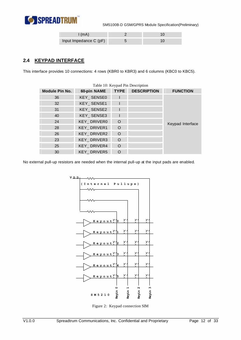
2.4 KEYPAD INTERFACE This interface provides 10 connections: 4 rows (KBR0 to KBR3) and 6 columns (KBC0 to KBC5).
Table 10: Keypad Pin Description Module Pin No. 60-pin NAME TYPE DESCRIPTION FUNCTION
36 KEY_ SENSE0 I
32 KEY_ SENSE1 I
31 KEY_ SENSE2 I
40 KEY_ SENSE3 I
24 KEY_ DRIVER0 O
28 KEY_ DRIVER1 O
26 KEY_ DRIVER2 O
23 KEY_ DRIVER3 O
25 KEY_ DRIVER4 O
30 KEY_ DRIVER5 O
Keypad Interface
No external pull-up resistors are needed when the internal pull-up at the input pads are enabled.
Keyout 0
Keyout 1
Keyout 2
Keyout 3
Keyout 4
Keyout 5
Keyi
n 0
Keyi
n 1
Keyi
n 2
Keyi
n 3
SM5210
VDD
(Internal Pullups)
Figure 2: Keypad connection SIM
SM5100B-D GSM/GPRS Module Specification(Preliminary) ————————————————————————————————————————————————————————————
V1.0.0 Spreadtrum Communications, Inc. Confidential and Proprietary Page 13 of 33
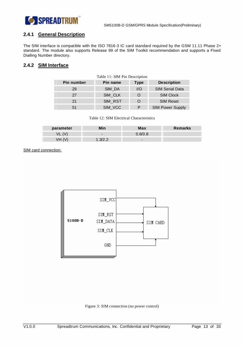
2.4.1 General Description The SIM interface is compatible with the ISO 7816-3 IC card standard required by the GSM 11.11 Phase 2+ standard. The module also supports Release 99 of the SIM Toolkit recommendation and supports a Fixed Dialling Number directory.
2.4.2 SIM Interface
Table 11: SIM Pin Description Pin number Pin name Type Description
29 SIM_DA I/O SIM Serial Data
27 SIM_CLK O SIM Clock
21 SIM_RST O SIM Reset
51 SIM_VCC P SIM Power Supply
Table 12: SIM Electrical Characteristics
parameter Min Max Remarks VL (V) - 0.6/0.8 VH (V) 1.3/2.2 -
SIM card connection:
Figure 3: SIM connection (no power control)
SM5100B-D GSM/GPRS Module Specification(Preliminary) ————————————————————————————————————————————————————————————
V1.0.0 Spreadtrum Communications, Inc. Confidential and Proprietary Page 14 of 33
Figure 4 shows system design for 3.0V and 1.8V SIM card interface. The SIM level shift is built in the SC6600D chip. Note: 1)SIM_VCC need add three capacitor: 4.7uF,0.1uF, 27pF. 2)SIM_RST,SIM_DATA,SIM_CLK lines also need add 27pF capacitor for each line. 3) SIM_DATA need to Pull-up with 2K resistor to SIM_VCC. NOTES: Does not support 5V SIM card.
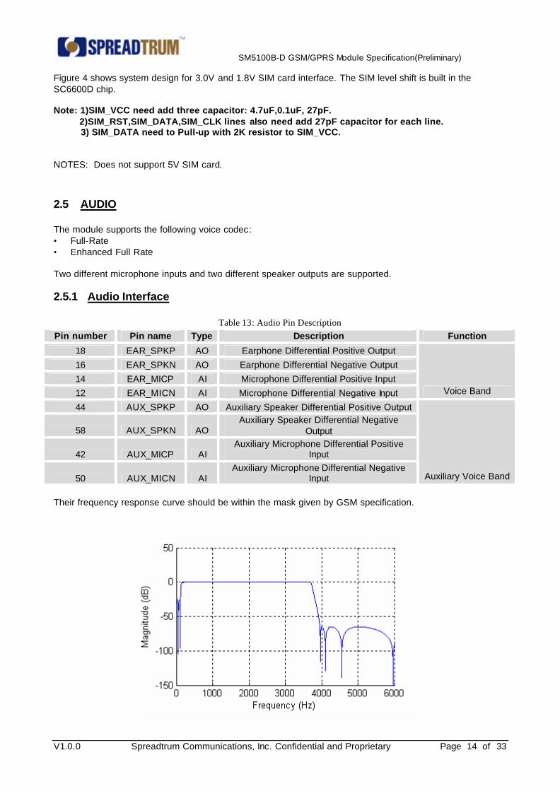
2.5 AUDIO The module supports the following voice codec: • Full-Rate • Enhanced Full Rate Two different microphone inputs and two different speaker outputs are supported.
2.5.1 Audio Interface
Table 13: Audio Pin Description Pin number Pin name Type Description Function
18 EAR_SPKP AO Earphone Differential Positive Output
16 EAR_SPKN AO Earphone Differential Negative Output
14 EAR_MICP AI Microphone Differential Positive Input
12 EAR_MICN AI Microphone Differential Negative Input Voice Band
44 AUX_SPKP AO Auxiliary Speaker Differential Positive Output
58 AUX_SPKN AO Auxiliary Speaker Differential Negative
Output
42 AUX_MICP AI Auxiliary Microphone Differential Positive
Input
50 AUX_MICN AI Auxiliary Microphone Differential Negative
Input Auxiliary Voice Band
Their frequency response curve should be within the mask given by GSM specification.
SM5100B-D GSM/GPRS Module Specification(Preliminary) ————————————————————————————————————————————————————————————
V1.0.0 Spreadtrum Communications, Inc. Confidential and Proprietary Page 15 of 33
Figure 4: Audio Frequency Response Curve
2.5.2 Typical Microphone Inputs Characteristics The gain of MIC inputs is internally adjusted and can be turned from 9dB to 42dB.
Table 14: Microphone Electrical Characteristics Parameter Conditions/Comments Min. Typ. Max. Units
Input common mode range 0.6 1.8 V PGA gain range 9 42 dB
Maximum analog input range after PGA Differential ±1.5 V
Digital audio output sample rate 8 kHz ADC resolution 13 bits
ADC signal to (noise + distortion) ratio 62 dB Digital output word 16 bits
2.5.3 Typical Speaker Outputs Characteris tics The gain of speaker outputs is internally adjusted and can be turned from -21dB to 12dB
Table 15: Speaker Electrical Characteristics Parameter Conditions/Comments Min. Typ. Max. Units
Maximum differential output voltage ±1.4 V Maximum single-ended output voltage 1.4 V
Output common mode voltage 1.1 V Minimum load resistance 16 Ω
gain range -21 12 dB
2.5.4 Typical Microphone Connection Two MIC inputs already include the biasing for an electret microphone allowing easy connection to the headset. The connection can be either differential or single ended; but using a differential connection in order to reject common mode noise TDMA noise is strongly recommended. • Recommended characteristics for the microphone Type: Electret • Impedance: 2.2Kohm • Sensitivity: -42dB(typ) • SNR > 50dB min • Frequency response compatible with the GSM specifications
2.5.4.1 Differential Connection
SM5100B-D GSM/GPRS Module Specification(Preliminary) ————————————————————————————————————————————————————————————
V1.0.0 Spreadtrum Communications, Inc. Confidential and Proprietary Page 16 of 33
C1 C2
C4
C3L 1
L 2
MICP
MICN
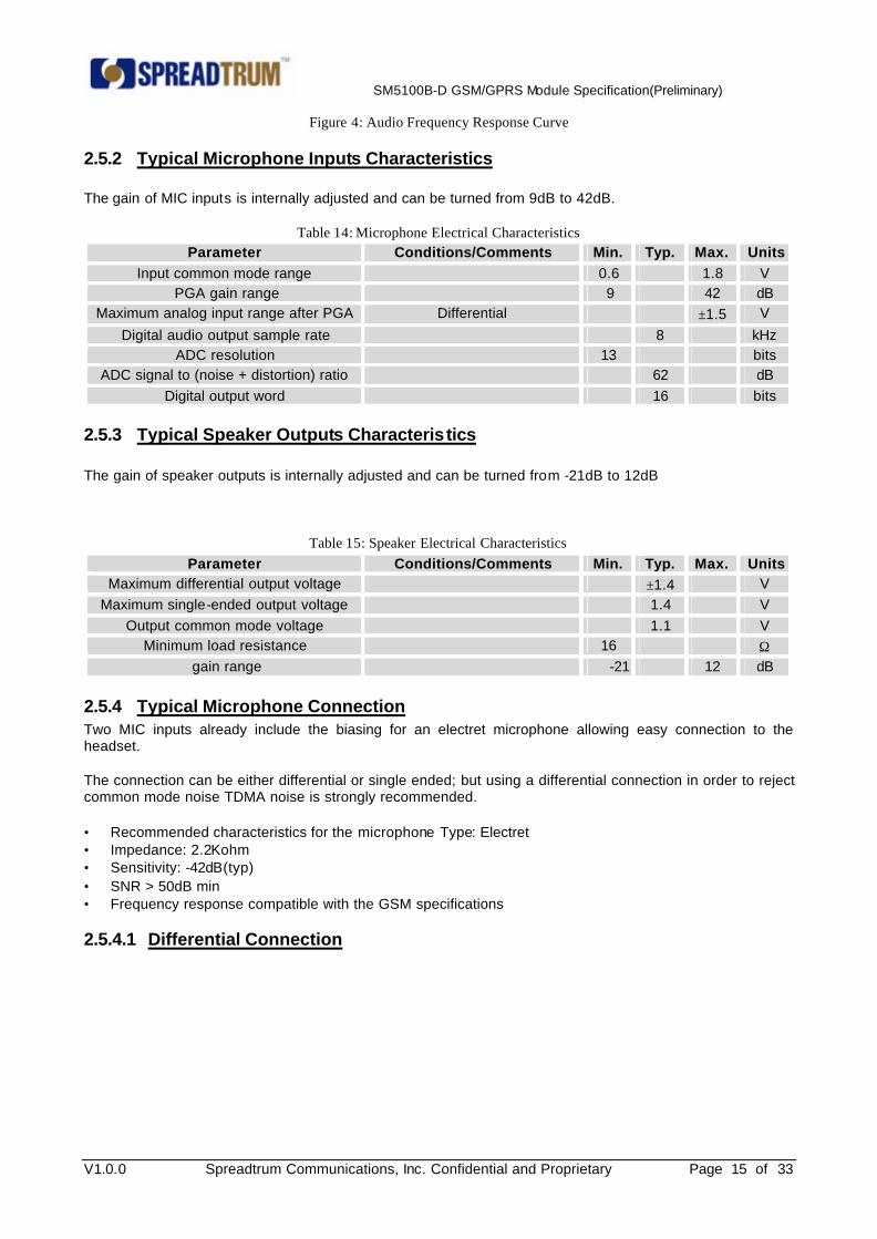
Figure 5: MIC input (differential input)
The recommended characteristic of capacitors: C1=22pF to 47pF C2=C3=C4=47pF to 100pF L1=L2=100nH Microphone manufacturer can provide a microphone soldered C1 directly on it, so that C1 can be the nearest to the Microphone.
2.5.4.2 Single-ended Connection
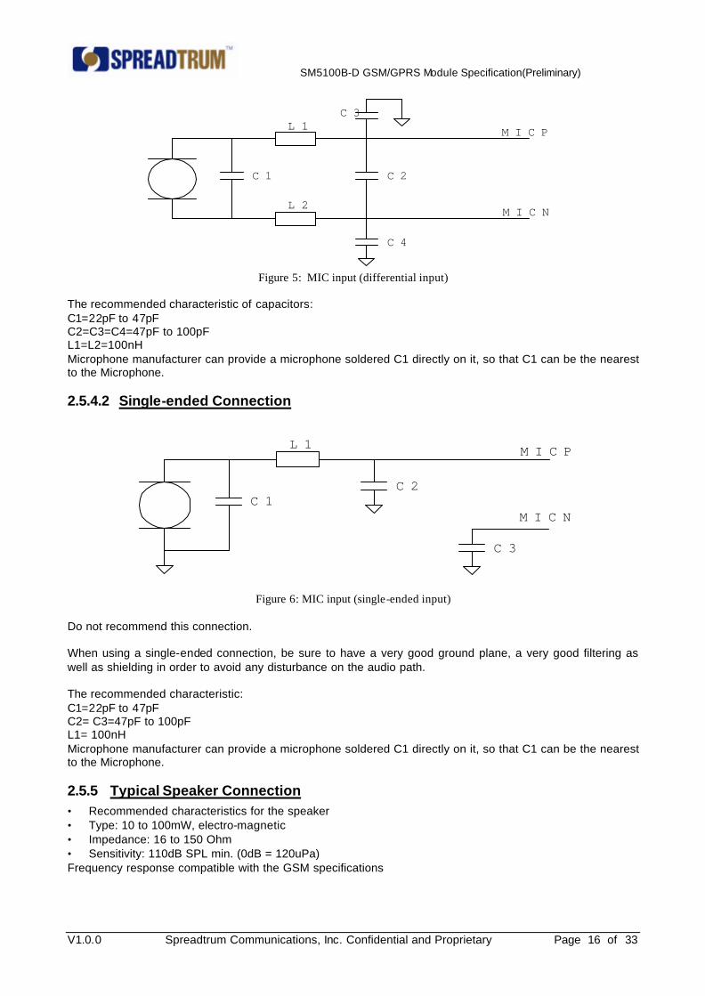
C1C2
L1 MICP
C3
MICN
Figure 6: MIC input (single-ended input) Do not recommend this connection. When using a single-ended connection, be sure to have a very good ground plane, a very good filtering as well as shielding in order to avoid any disturbance on the audio path. The recommended characteristic: C1=22pF to 47pF C2= C3=47pF to 100pF L1= 100nH Microphone manufacturer can provide a microphone soldered C1 directly on it, so that C1 can be the nearest to the Microphone.
2.5.5 Typical Speaker Connection • Recommended characteristics for the speaker • Type: 10 to 100mW, electro-magnetic • Impedance: 16 to 150 Ohm • Sensitivity: 110dB SPL min. (0dB = 120uPa) Frequency response compatible with the GSM specifications
SM5100B-D GSM/GPRS Module Specification(Preliminary) ————————————————————————————————————————————————————————————
V1.0.0 Spreadtrum Communications, Inc. Confidential and Proprietary Page 17 of 33
2.5.5.1 Differential Connection
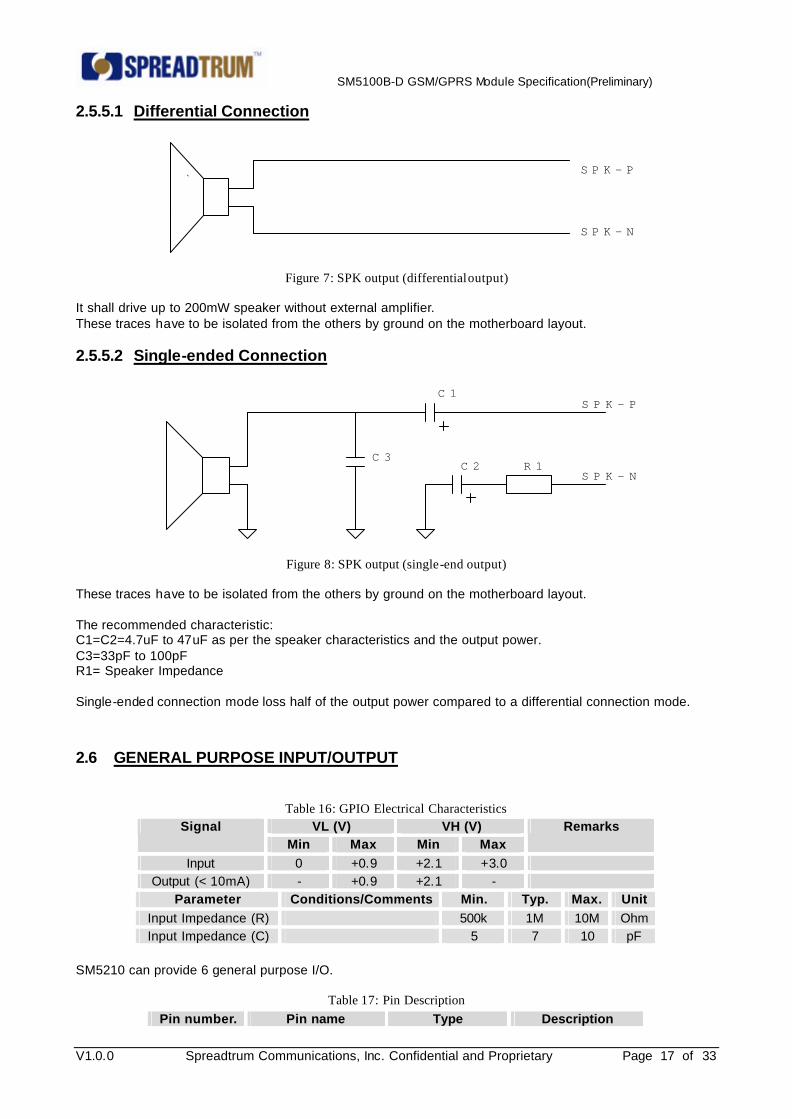
`SPK-P
SPK-N
Figure 7: SPK output (differential output) It shall drive up to 200mW speaker without external amplifier. These traces have to be isolated from the others by ground on the motherboard layout.
2.5.5.2 Single-ended Connection
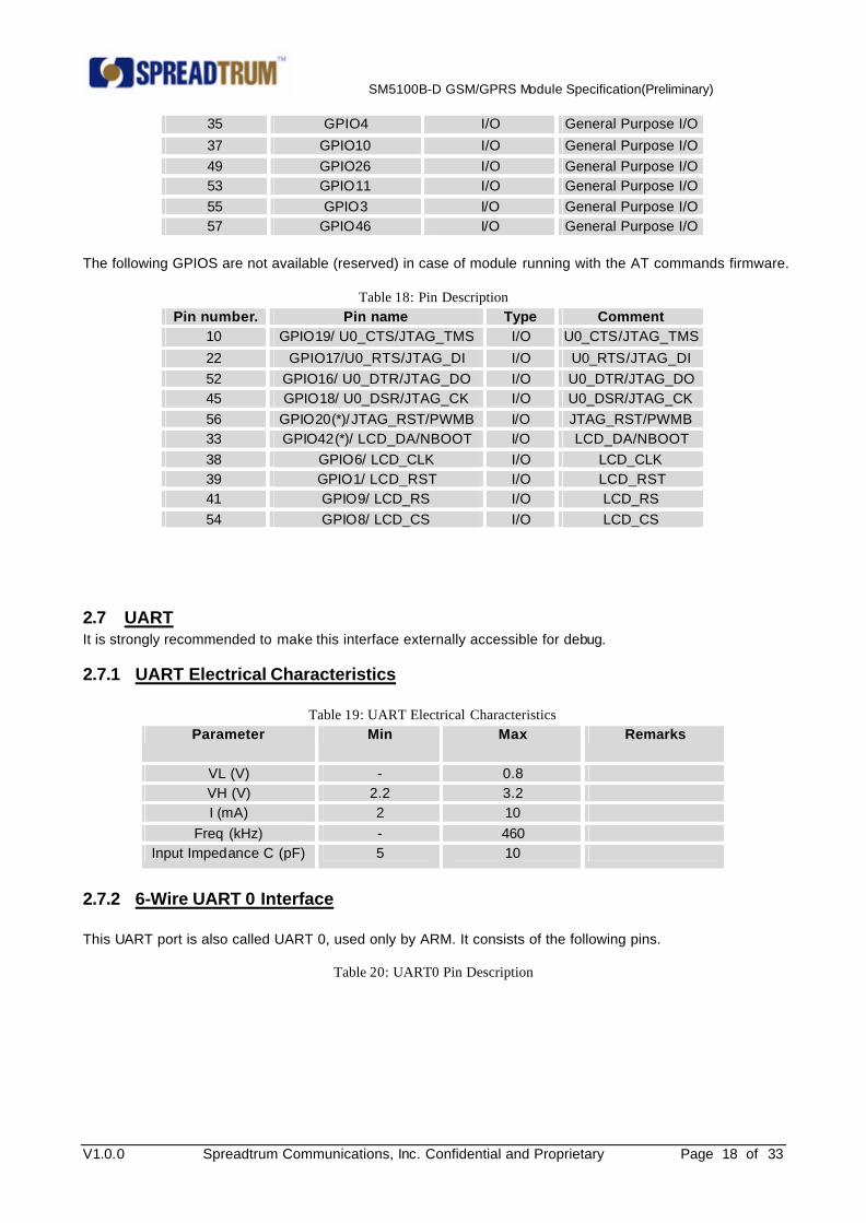
SPK-P
SPK-N
C1
C2C3
R1
Figure 8: SPK output (single-end output) These traces have to be isolated from the others by ground on the motherboard layout. The recommended characteristic: C1=C2=4.7uF to 47uF as per the speaker characteristics and the output power. C3=33pF to 100pF R1= Speaker Impedance Single-ended connection mode loss half of the output power compared to a differential connection mode.
2.6 GENERAL PURPOSE INPUT/OUTPUT
Table 16: GPIO Electrical Characteristics VL (V) VH (V) Signal
Min Max Min Max Remarks
Input 0 +0.9 +2.1 +3.0 Output (< 10mA) - +0.9 +2.1 -
Parameter Conditions/Comments Min. Typ. Max. Unit Input Impedance (R) 500k 1M 10M Ohm Input Impedance (C) 5 7 10 pF
SM5210 can provide 6 general purpose I/O.
Table 17: Pin Description Pin number. Pin name Type Description
SM5100B-D GSM/GPRS Module Specification(Preliminary) ————————————————————————————————————————————————————————————
V1.0.0 Spreadtrum Communications, Inc. Confidential and Proprietary Page 18 of 33
35 GPIO4 I/O General Purpose I/O
37 GPIO10 I/O General Purpose I/O 49 GPIO26 I/O General Purpose I/O 53 GPIO11 I/O General Purpose I/O 55 GPIO3 I/O General Purpose I/O 57 GPIO46 I/O General Purpose I/O
The following GPIOS are not available (reserved) in case of module running with the AT commands firmware.
Table 18: Pin Description Pin number. Pin name Type Comment
10 GPIO19/ U0_CTS/JTAG_TMS I/O U0_CTS/JTAG_TMS
22 GPIO17/U0_RTS/JTAG_DI I/O U0_RTS/JTAG_DI 52 GPIO16/ U0_DTR/JTAG_DO I/O U0_DTR/JTAG_DO 45 GPIO18/ U0_DSR/JTAG_CK I/O U0_DSR/JTAG_CK 56 GPIO20(*)/JTAG_RST/PWMB I/O JTAG_RST/PWMB 33 GPIO42(*)/ LCD_DA/NBOOT I/O LCD_DA/NBOOT 38 GPIO6/ LCD_CLK I/O LCD_CLK 39 GPIO1/ LCD_RST I/O LCD_RST 41 GPIO9/ LCD_RS I/O LCD_RS 54 GPIO8/ LCD_CS I/O LCD_CS
2.7 UART It is strongly recommended to make this interface externally accessible for debug.
2.7.1 UART Electrical Characteristics
Table 19: UART Electrical Characteristics Parameter Min Max Remarks
VL (V) - 0.8 VH (V) 2.2 3.2 I (mA) 2 10
Freq (kHz) - 460 Input Impedance C (pF) 5 10
2.7.2 6-Wire UART 0 Interface This UART port is also called UART 0, used only by ARM. It consists of the following pins.
Table 20: UART0 Pin Description
SM5100B-D GSM/GPRS Module Specification(Preliminary) ————————————————————————————————————————————————————————————
V1.0.0 Spreadtrum Communications, Inc. Confidential and Proprietary Page 19 of 33
The hardware flow control pins are also shared with JTAG pins. When JTAG is used, only RX and TX pins are available, reducing to a 2-wire UART port. UART's rate is up to 460kbps max.
2.7.3 2-Wire UART 1 Interface This UART is also called UART 1 and can be used by either ARM or TeakLite. It consists of the following pins.
Table 21:UART1 Pin Description Module Pin No. 60-pin NAME TYPE SIGNAL DESCRIPTION
46 TX1 O TXD Transmit Data 43 RX1 I RXD Receive Data
There is no hardware flow control for this UART interface. UART's rate is up to 460kbps max.
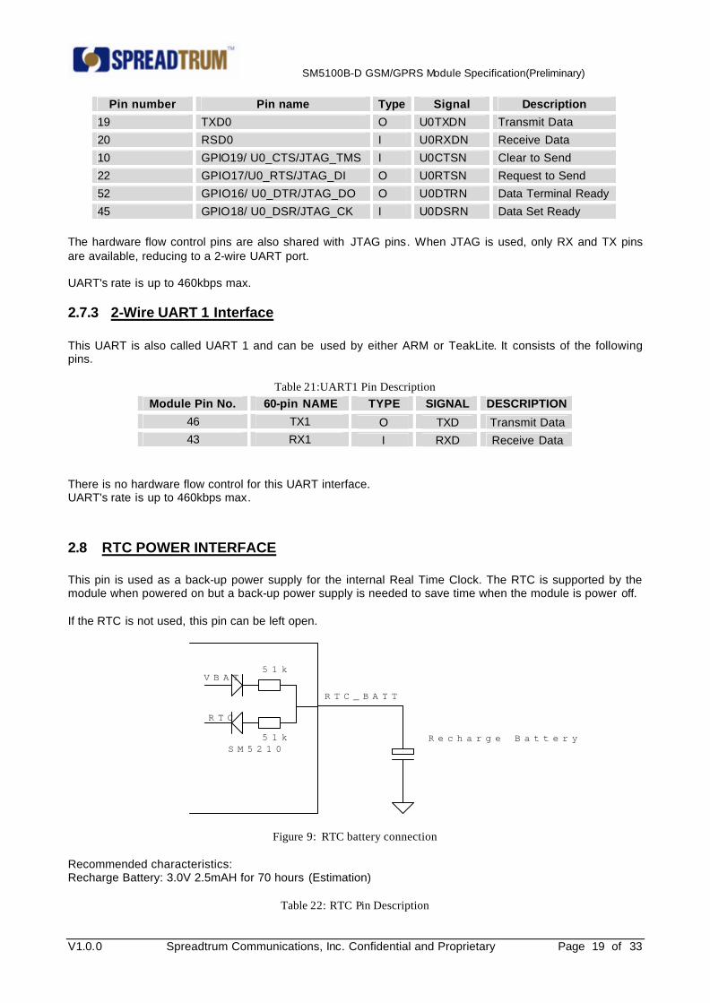
2.8 RTC POWER INTERFACE This pin is used as a back-up power supply for the internal Real Time Clock. The RTC is supported by the module when powered on but a back-up power supply is needed to save time when the module is power off. If the RTC is not used, this pin can be left open.
RTC_BATT
SM5210Recharge Battery
VBAT
RTC
51k
51k
Figure 9: RTC battery connection Recommended characteristics: Recharge Battery: 3.0V 2.5mAH for 70 hours (Estimation)
Table 22: RTC Pin Description
Pin number Pin name Type Signal Description
19 TXD0 O U0TXDN Transmit Data
20 RSD0 I U0RXDN Receive Data
10 GPIO19/ U0_CTS/JTAG_TMS I U0CTSN Clear to Send
22 GPIO17/U0_RTS/JTAG_DI O U0RTSN Request to Send
52 GPIO16/ U0_DTR/JTAG_DO O U0DTRN Data Terminal Ready
45 GPIO18/ U0_DSR/JTAG_CK I U0DSRN Data Set Ready
SM5100B-D GSM/GPRS Module Specification(Preliminary) ————————————————————————————————————————————————————————————
V1.0.0 Spreadtrum Communications, Inc. Confidential and Proprietary Page 20 of 33
Pin number Pin name Type Description
48 RTC_BATT Supply Power Supply for RTC
Table 23: RTC Electrical Characteristics Parameter Min. Typ. Max.
V (V) 2.7 3.0 3.3 I (uA) 15 15 25
2.9 ADC Interface The SM5210 can provide two ADC ports ranging from 0.1 to 1.2V, 0 to 8V
Table 24: ADC Pin Description Pin number. Pin name TYPE DESCRIPTION Input Rang
6 ADCIN1 AI A/D Converter 0.3~3.0V
8 ADCIN2 AI A/D Converter 0.3~3.0V
Table 25: ADC Electrical Characteristics Parameter Conditions/Comments Min. Typ. Max. Unit Resolution Guaranteed monotonic to 9 bits 10 bits
Integral non-linearity ±3 LSB Differential non-linearity ±2 LSB
Number of input channels 4 Conversion time 15 µs
Power up settling time 10 µs Input Impedance (C) 5 7 10 pF
2.10 Reset This signal is used to force a reset procedure by providing a low level voltage during at least 100µs. This signal has to be considered as an emergency reset only. A reset procedure is already driven by an internal hardware during the power-on sequence. This pin function is only for NOR flash RESET. This signal is only an internal reset. It can not be used to provide a reset to an external device. Reset process is activated either by the external reset signal or by an internal signal (coming from a reset generator). This automatic reset is activated at power-up. The pin is held low at power-up. An internal capacitor can provide a 100µs delay. If an external capacitor is connected at the RESET pin, the delay would be
Tdelay = 1 ms * Cextcap / 100 pF
Table 26: Pin Description
Pin number Pin name Type Description
34 RESET I Asynchronous Reset, active low
SM5100B-D GSM/GPRS Module Specification(Preliminary) ————————————————————————————————————————————————————————————
V1.0.0 Spreadtrum Communications, Inc. Confidential and Proprietary Page 21 of 33
Table 27: Electrical Characteristics Parameter Min Max
VL (V) - 0.8 VH (V) 2.2 - I (mA) 2 10
Input Impedance C (pF) Input Impedance R (Kohm)
2.11 Power On Interface This input is to switch ON SM5210 module. A high level voltage has to be provided on this pin to switch on the module. After the module is switched on, this pin will be set as GPIO, the Power ON function will be screened. NOTES: There are no Power OFF functions on this pin.
Table 28: Pin Description
Pin number Pin name Type Description
59 POWER_ON I Module Power ON ,High Active
Table 29: Power-On Electrical Characteristics Parameter Min Max
VL (V) - 0.8 VH (V) 2.2 - I (mA) 2 10
Input Impedance C (pF) Input Impedance R (Kohm)
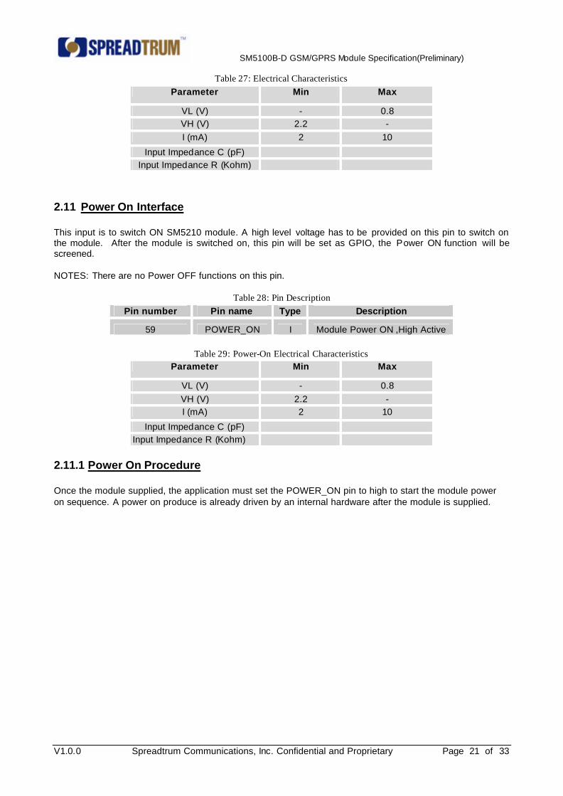
2.11.1 Power On Procedure Once the module supplied, the application must set the POWER_ON pin to high to start the module power on sequence. A power on produce is already driven by an internal hardware after the module is supplied.
SM5100B-D GSM/GPRS Module Specification(Preliminary) ————————————————————————————————————————————————————————————
V1.0.0 Spreadtrum Communications, Inc. Confidential and Proprietary Page 22 of 33
Power on Button down1s min
Tdelay=200us
/RESET
POWER ON
POWERSUPPLY
MODULE STATUSOFF MODE
I<30uA
RESET MODE
I<13mA
IDLE MODE
I<3mA
Communicaito mode
I<250mA(AVERAGE)
AT COMMARD READYT=2 ms
Figure 10: Power-on Sequence
I = overall current consumption (Base Band + RF Band)
2.12 NORMAL/BOOT This input is used to setting the module booting mode. Here is the function description: · Low during reset: Download mode. · High during reset: Normal-working mode. In the normal working mode, the handset action is supported by the normal phone call software. Since the CPU takes its level during reset, the pin can be used for other function after reset.
Table 30: Pin Description
Pin number Pin name Type Description
33 GPO42/LCD_DA/NBOOT O Boot mode setting
2.13 BATTERY CHARGING INTERFACE (OPTIONAL)
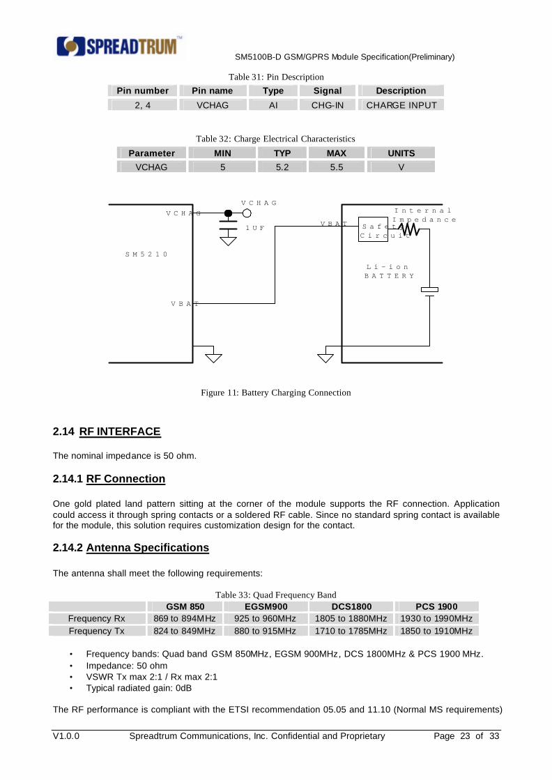
2.13.1 Li-ion Battery Charge Interface SM5210 module supports one Li-ion battery charging. The charging circuit is built in the module. The circuit use an interface VCHG to supply a constant charge current. This current value depends on the battery capacity. It is recommended to provide a current of 2/3C. The current default charge setting in module is 500mA. SM5210 module also can monitor the battery voltage, and detect the end of the charge. This function is built in the module
SM5100B-D GSM/GPRS Module Specification(Preliminary) ————————————————————————————————————————————————————————————
V1.0.0 Spreadtrum Communications, Inc. Confidential and Proprietary Page 23 of 33
Table 31: Pin Description
Pin number Pin name Type Signal Description
2, 4 VCHAG AI CHG-IN CHARGE INPUT
Table 32: Charge Electrical Characteristics
Parameter MIN TYP MAX UNITS
VCHAG 5 5.2 5.5 V
VCHAGVCHAG
1UF
SM5210
VBAT
VBAT
SafetyCircuit
InternalImpedance
Li-ionBATTERY
Figure 11: Battery Charging Connection
2.14 RF INTERFACE The nominal impedance is 50 ohm.
2.14.1 RF Connection One gold plated land pattern sitting at the corner of the module supports the RF connection. Application could access it through spring contacts or a soldered RF cable. Since no standard spring contact is available for the module, this solution requires customization design for the contact.
2.14.2 Antenna Specifications The antenna shall meet the following requirements:
Table 33: Quad Frequency Band GSM 850 EGSM900 DCS1800 PCS 1900
Frequency Rx 869 to 894MHz 925 to 960MHz 1805 to 1880MHz 1930 to 1990MHz Frequency Tx 824 to 849MHz 880 to 915MHz 1710 to 1785MHz 1850 to 1910MHz
• Frequency bands: Quad band GSM 850MHz, EGSM 900MHz, DCS 1800MHz & PCS 1900 MHz. • Impedance: 50 ohm • VSWR Tx max 2:1 / Rx max 2:1 • Typical radiated gain: 0dB
The RF performance is compliant with the ETSI recommendation 05.05 and 11.10 (Normal MS requirements)
SM5100B-D GSM/GPRS Module Specification(Preliminary) ————————————————————————————————————————————————————————————
V1.0.0 Spreadtrum Communications, Inc. Confidential and Proprietary Page 24 of 33
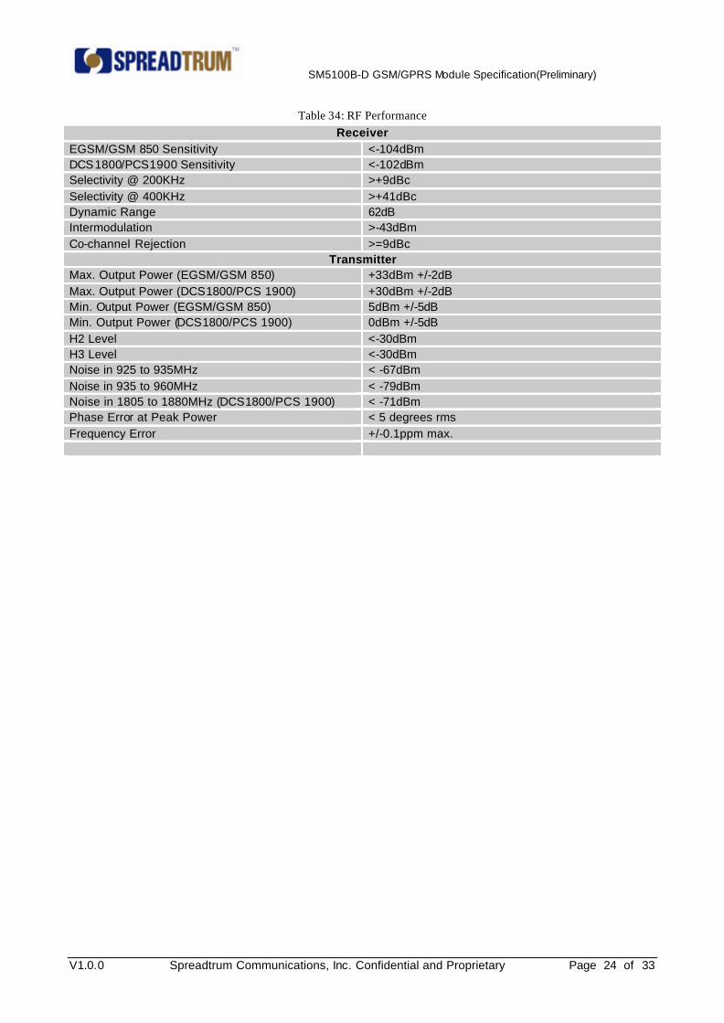
Table 34: RF Performance
Receiver EGSM/GSM 850 Sensitivity <-104dBm DCS1800/PCS1900 Sensitivity <-102dBm Selectivity @ 200KHz >+9dBc Selectivity @ 400KHz >+41dBc Dynamic Range 62dB Intermodulation >-43dBm Co-channel Rejection >=9dBc
Transmitter Max. Output Power (EGSM/GSM 850) +33dBm +/-2dB Max. Output Power (DCS1800/PCS 1900) +30dBm +/-2dB Min. Output Power (EGSM/GSM 850) 5dBm +/-5dB Min. Output Power (DCS1800/PCS 1900) 0dBm +/-5dB H2 Level <-30dBm H3 Level <-30dBm Noise in 925 to 935MHz < -67dBm Noise in 935 to 960MHz < -79dBm Noise in 1805 to 1880MHz (DCS1800/PCS 1900) < -71dBm Phase Error at Peak Power < 5 degrees rms Frequency Error +/-0.1ppm max.
SM5100B-D GSM/GPRS Module Specification(Preliminary) ————————————————————————————————————————————————————————————
V1.0.0 Spreadtrum Communications, Inc. Confidential and Proprietary Page 25 of 33
3 TECHNICAL SPECIFICATIONS
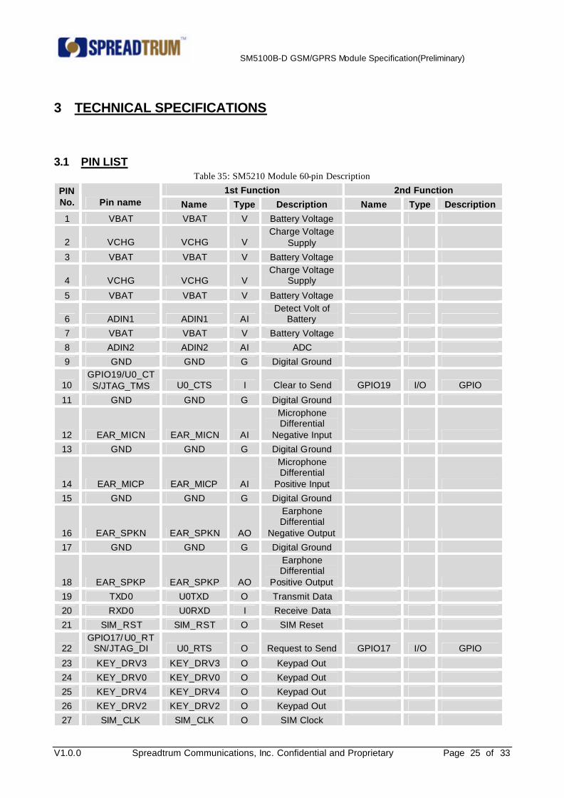
3.1 PIN LIST Table 35: SM5210 Module 60-pin Description
1st Function 2nd Function PIN No. Pin name Name Type Description Name Type Description
1 VBAT VBAT V Battery Voltage
2 VCHG VCHG V Charge Voltage
Supply
3 VBAT VBAT V Battery Voltage
4 VCHG VCHG V Charge Voltage
Supply
5 VBAT VBAT V Battery Voltage
6 ADIN1 ADIN1 AI Detect Volt of
Battery
7 VBAT VBAT V Battery Voltage
8 ADIN2 ADIN2 AI ADC
9 GND GND G Digital Ground
10 GPIO19/U0_CTS/JTAG_TMS U0_CTS I Clear to Send GPIO19 I/O GPIO
11 GND GND G Digital Ground
12 EAR_MICN EAR_MICN AI
Microphone Differential
Negative Input
13 GND GND G Digital Ground
14 EAR_MICP EAR_MICP AI
Microphone Differential
Positive Input
15 GND GND G Digital Ground
16 EAR_SPKN EAR_SPKN AO
Earphone Differential
Negative Output
17 GND GND G Digital Ground
18 EAR_SPKP EAR_SPKP AO
Earphone Differential
Positive Output
19 TXD0 U0TXD O Transmit Data
20 RXD0 U0RXD I Receive Data
21 SIM_RST SIM_RST O SIM Reset
22 GPIO17/ U0_RT
SN/JTAG_DI U0_RTS O Request to Send GPIO17 I/O GPIO
23 KEY_DRV3 KEY_DRV3 O Keypad Out
24 KEY_DRV0 KEY_DRV0 O Keypad Out
25 KEY_DRV4 KEY_DRV4 O Keypad Out
26 KEY_DRV2 KEY_DRV2 O Keypad Out
27 SIM_CLK SIM_CLK O SIM Clock
SM5100B-D GSM/GPRS Module Specification(Preliminary) ————————————————————————————————————————————————————————————
V1.0.0 Spreadtrum Communications, Inc. Confidential and Proprietary Page 26 of 33
28 KEY_DRV1 KEY_DRV1 O Keypad Out
29 SIM_DA SIM_DA I/O SIM Serial Data
30 KBY_DRV5 KEY_DRV5 O Keypad Out
31 KEY_SEN2 KEY_SEN2 I Keypad Input
32 KEY_SEN1 KEY_SEN1 I Keypad Input
33 GPO42/ LCD_D
A/NBOOT LCD-DATA O LCD_DATA_SPI NBOOT I BOOT
34 RESET RESET I Asynchronous
reset, active low
35 GPIO4/HF_CTR
L GPIO4 I/O GPIO
36 KEY_SEN0 KEY_SEN0 I Keypad Input
37 GPIO10/CHAR
GE_IN GPIO10 I/O GPIO
38 GPIO6/LCD_CL
K LCD-CLK O LCD_CLK_SPI GPIO6 I/O GPIO
39 GPIO1/LCD_RS
T LCD-RST O LCD_RST_SPI GPIO1 I/O GPIO
40 KEY_SEN3 KEY_SEN3 I Keypad Input
41 GPIO9/LCD_RS LCD_RS O LCD_RS_SPI GPIO9 I/O GPIO
42 AUX_MICP AUX_MICP AI
Auxiliary Microphone Differential
Positive Input
43 RXD1 RXD1 I Receive Data
44 AUX_SPKP AUX_SPKP AO
Auxiliary Speaker
Differential Positive Output
45 GPIO18/U0_DS
R/JTAG_CK U0_DSR I Data Set Ready GPIO18 I/O GPIO
46 TXD1 TXD1 O Transmit Data
47 VCC VCC V 2.8V POWER
SUPPLY 50mA
48 RTC_BATT RTC_BATT V RTCVDD 3.0V
49 GPIO26/LED_B
K_CTRL GPIO26 I/O GPIO
50 AUX_MICN AUX_MICN AI
Auxiliary Microphone Differential
Negative Input
51 SIM_VCC SIM_VCC V SIM POWER 3V
52 GPIO16/U0_DT
R/JTAG_DO U0_DTR O Data Terminal
Ready GPIO16 I/O GPIO
53 GPO11/CS3 CS3 O ARM external
CS 3 GPO11 I/O GPIO
54 GPIO8/LCD_CS LCD_CS O LCD-CS-SPI GPIO8 I/O GPIO
55 GPIO3 GPIO3 I/O GPIO
56 GPIO20/JTAG_
RST/PWMB JTAG_RST O JTAT Reset GPIO20 I/O GPIO
57 GPIO46 GPIO46 I/O GPIO
58 AUX_SPKN AUX_SPKN AO Auxiliary
SM5100B-D GSM/GPRS Module Specification(Preliminary) ————————————————————————————————————————————————————————————
V1.0.0 Spreadtrum Communications, Inc. Confidential and Proprietary Page 27 of 33
Speaker Differential
Negative Output
59 POWER_ON POWER_ON I POWER Button
Interrupt
60 VCC VCC V 2.8V POWER
SUPPLY 50mA
3.2 ENVIRONMENTAL SPECIFICATIONS
Table 36: Module operating conditions Parameter Min Max
Normal operating range -10°C +55°C Supply voltage Vbat +3.3V +4.2V
Table 37: Ambient Temperature Conditions
Parameter Min Max Ambient temperature -10°C +55°C Storage temperature -40°C +85°C
SM5100B-D GSM/GPRS Module Specification(Preliminary) ————————————————————————————————————————————————————————————
V1.0.0 Spreadtrum Communications, Inc. Confidential and Proprietary Page 28 of 33
4 DESIGN GUIDELINES
4.1 HARDWARE AND RF
4.1.1 EMC The EMC tests should be conducted at the early stage of any application to detect possible problems. More attention should be paid to the following issues during designs:
• Possible spurious or/and other unwanted emission radiated by the module to other RF receivers in the receiving band.
• ESD protection on SIM (if accessible from outside), serial link, … • EMC protection on audio inputs/outputs • Bias of the microphone inputs. • Ground plane location for microphones • Length of the SIM interface lines (preferably <10cm) • Metallic case or plastic casing with conductive paint is recommended.
4.1.2 Power Supply Power supply design is the key in the GSM terminal projects. A poor power supply design could affect in particular:
• EMC performances • Emission spectrum • Phase error and frequency error • Transmit power
Warning: Special attention should be paid to:
• Quality of the power supply such as low ripple, PWM converter preferred. • Capacity to deliver high current peaks in a short time (pulse radio emission) • Power supply can never be greater than 4.5 V.
4.1.3 Antenna Antenna structure and integration in the application is a major issue. Attention should be paid to:
• Selection of the antenna cable (performance, length, type, thermal resistance, etc.) • Selection of antenna connector (type, losses, mismatch, etc.) • Antenna isolation from digital circuits (including the interface signals)
A poor antenna could dramatically affect the GSM performance such as sensitivity and transmit power. Warning: Spreadtrum strongly recommends working with an antenna manufacturer either to develop an antenna for the application or to adapt an existing solution to the application. The antenna adaptation (mechanical and electrical adaptation) is one of the key issues in the design of a GSM terminal.
4.2 MECHANICAL INTEGRATION
SM5100B-D GSM/GPRS Module Specification(Preliminary) ————————————————————————————————————————————————————————————
V1.0.0 Spreadtrum Communications, Inc. Confidential and Proprietary Page 29 of 33
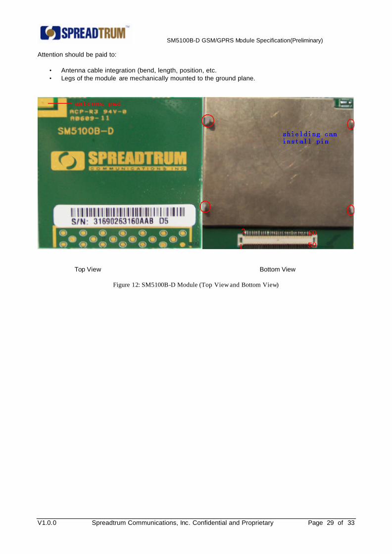
Attention should be paid to:
• Antenna cable integration (bend, length, position, etc. • Legs of the module are mechanically mounted to the ground plane.
Top View Bottom View
Figure 12: SM5100B-D Module (Top View and Bottom View)
SM5210 GSM/GPRS Module Specification(Preliminary) ———————————————————————————————————————————————————————————
V.1.0.0 Spreadtrum Communications, Inc. Confidential and Proprietary Page 30 of 33
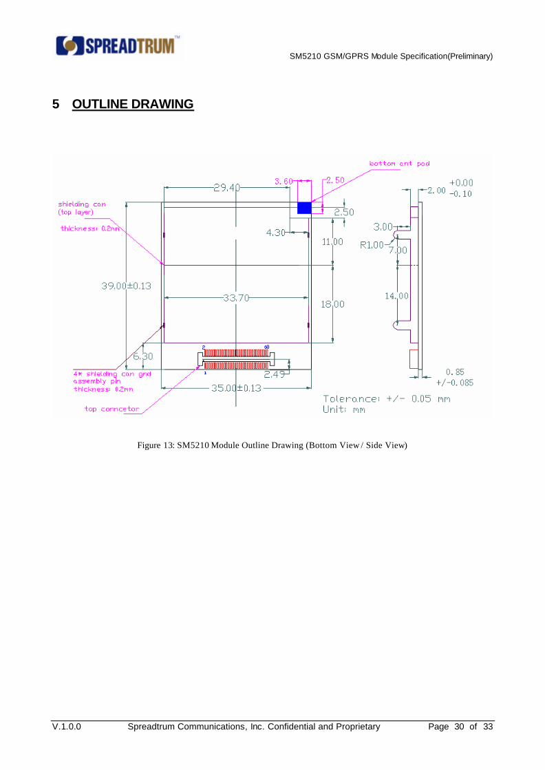
5 OUTLINE DRAWING
Figure 13: SM5210 Module Outline Drawing (Bottom View / Side View)
SM5210 GSM/GPRS Module Specification(Preliminary) ———————————————————————————————————————————————————————————
V.1.0.0 Spreadtrum Communications, Inc. Confidential and Proprietary Page 31 of 33
6 INTEGRATION
6.1 60-PIN CONNECTOR
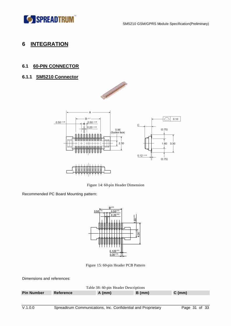
6.1.1 SM5210 Connector
Figure 14: 60-pin Header Dimension Recommended PC Board Mounting pattern:
Figure 15: 60-pin Header PCB Pattern
Dimensions and references:
Table 38: 60-pin Header Descriptions Pin Number Reference A (mm) B (mm) C (mm)
SM5210 GSM/GPRS Module Specification(Preliminary) ———————————————————————————————————————————————————————————
V.1.0.0 Spreadtrum Communications, Inc. Confidential and Proprietary Page 32 of 33
60 AXK6F60345P 28.00 24.5 1.25
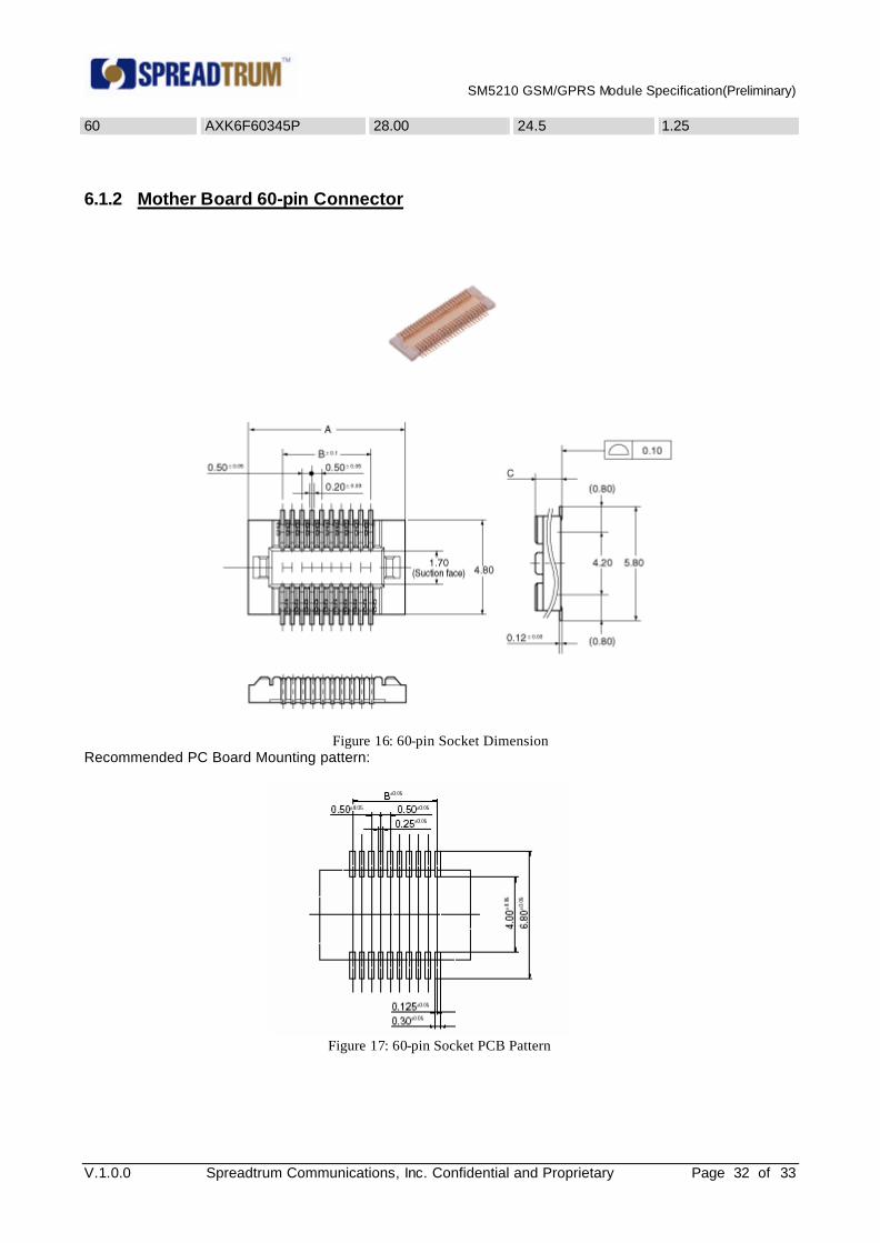
6.1.2 Mother Board 60-pin Connector
Figure 16: 60-pin Socket Dimension Recommended PC Board Mounting pattern:
Figure 17: 60-pin Socket PCB Pattern
SM5210 GSM/GPRS Module Specification(Preliminary) ———————————————————————————————————————————————————————————
V.1.0.0 Spreadtrum Communications, Inc. Confidential and Proprietary Page 33 of 33
Dimensions and references:
Table 39: 60-pin Socket Descriptions Pin Number References A (mm) B(mm) C(mm) 60 AXK5F60545P 28.00 24.50 1.85
END OF DOCUMENT


![SM5100B-D GSM/GPRS Module Hardware Specification · SM5100B-D GSM/GPRS Module Hardware Specification 2 Product concept . SM5100B-D is a Dual-Band EGSM900/DCS1800[*2] GSM/GPRS module](https://img.pdfslide.net/doc/110x75/5e2e01faf5dc2f700f118a9d/sm5100b-d-gsmgprs-module-hardware-specification-sm5100b-d-gsmgprs-module-hardware.jpg)