Embed Size (px)
Citation preview
Small signal analysis of dual input buck converter
M M Alam , D C Lu,Y Siwakoti
School of Electrical and Data Engineering, University of Technology Sydney, 2007, Australia
Abstract
This paper presents a small signal modelling and voltage-mode control of a pulse-width modulated (PWM) dual-input
DC-DC buck converter. The control of multiple switches in a power converter is the main challenge for multiple-
input converters addressed in this paper. Using the concept of linearization and perturbation depicted in circuit
averaging technique, the closed-loop small signal model for multi-input DC-DC buck converter is derived. The
closed loop control to output voltage transfer function is derived. A brief compensator design is introduced for a
multi-input buck converter. In order to control the duty cycles of multiple switches and control the output voltage, a
new variable is introduced to relate the duty cycles in the closed loop control to output voltage transfer function. The
analysis and controller design are simulated in LTSpice. Keywords: Small Signal Model, Pulse Width Modulation (PWM), DC/DC Buck Converter
1 . Introduction
Nowadays, the power generation sector is inclining towards the use of renewable energy resources in
every field such as residential, automotive and aerospace. The main reason behind using renewable
resources is their environmental-friendliness, which makes them a better alternative as compared to
conventional power generation techniques. However, the performance and reliability of renewable
resources is remarkably affected by their intermittent nature [1]. This intermittent nature is badly affecting
the complete unification of power generation with renewable resources. Therefore, the optimal solution of
this intermittent nature is the combination of renewable resources with various other energy resources [2].
The integration of renewable resources with other energy resources provides the basis of using and
analysing power converters. In general, the integration of each energy module into a system requires a dc-
dc converter that can result into less efficient, bulky system with more control problems [3]. Therefore,
the combination of resources requires a reliable multiple input power converter having an ability to
accommodate more than one inputs of energy resources and provide the output/s according to the user’s
requirement.
With the help of using the multiple-input converters, the energy can be utilised better and it can also
increase the reliability of the overall system [4]. Utilising multiple-input converter can result in different
advantages such as less component count, smaller size and control simplicity [5].The authors in literature
[6-8] discussed and analysed several dc-dc multiple-input converters including double-input buck, boost
and buck-buck boost converters. A brief comparison study between different converter designs is
discussed in [9] where the authors compared various converter topologies on the basis of component
count, reliability aspect and the flexibility of the resources. The control objectives of different converter
topologies are discussed in [10-14] as it is outlined as the essential part of these topologies. In [10], the
authors tried to keep one of the source current as constant with the output voltage regulation in double-
input buck-buck boost topology. In [15], the control objective of a double-input buck-boost converter is
discussed where the author introduced the concept of power sharing during the load variations of the
resources. Finally in [16], the author performed small signal modelling for double-input buck boost
* Manuscript received December 7, 2018; revised November 15, 2019.
Corresponding author. E-mail address: [email protected].
International Journal of Smart Grid and Clean Energy
doi: 10.12720/sgce.9.1.8-16
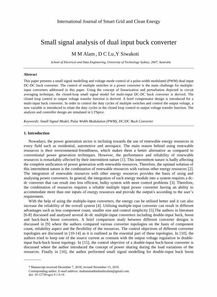
converter but so far, there is no small signal model introduced for double-input dc-dc converter with a
simple control strategy. Following the same concept, this paper discussed the small signal modelling and
stable control system for a particular circuit topology depicted in Fig. 1.
In this paper, the small signal modelling for multi-input buck converter is discussed in Section 2. In
section 3 the steps involved in designing the control of the circuit are explained. In Section 4, the
simulation and experimental results will be analysed according to the initial requirements followed by the
concluding remarks about selected multiple-input single output topology.
2. Small Signal Modelling of DISO Buck Converter
In order to design a stable control system, this paper analysed the control strategies discussed in [16-
19]. In [16], the author proposed a control strategy depending upon independent control of two loops.
One control loop was designed for current control while the second loop was controlling the voltage. In
this way, the loops were controlling the duty cycles of both the switches independently. One of the
limitations of this control strategy was its level of complexity. Another research study in [18] introduced
an idea of controlling three switches by a new control strategy. According to the author, a different PWM
technique was employed by using two saw tooth waveform carriers. The author used an up-counting saw-
tooth wave form for one switch while a down-counting saw tooth waveform for the other switch giving a
phase difference of 180 degrees [18]. With the help of this technique, the author tried to avoid turning on
both switches at the same time without using an external circuit. The two saw tooth waveforms along
with the feedback controller providing different duty cycles in order to control the output. The major
drawback of this strategy is its application, the strategy is applicable only for the circuit introduced in [18].
While searching for other control strategies, the paper also analysed a simple PWM control strategy
introduced in [19]. The author found that circuit is working in two modes i.e. Boost & Buck. Depending
upon the boost required for stability, the author used two different negative feedback controllers for the
voltage mode control for the circuit. The control strategy in the voltage mode control is controlling one
switch by adding both duty cycles and the other switch is controlled by giving a single duty cycle. The
limitation of this technique is again its application, as the control strategy was defined more specifically
for the circuitry used in [19]. After analysing all the research papers, this paper is going to discuss a new
control strategy for a different multi-input buck converter by following the same steps used in [19].
Proceeding the concept of small signal modelling introduced in [16], this paper will apply small signal
analysis for a voltage mode control multi-port buck converter using a negative feedback controller. The
author in [16] stated all power converters regardless of their topologies, are non-linear systems. Moreover,
authors also stated in [16] before using these converters topologies, the systems needs to be linearize by
performing small signal modelling. After performing small signal modelling, the feedback controllers can
be designed depending upon the linear time invariant models in order to get desired results [20].
Fig. 1. Dual input buck converter
9Muhammad Alam et al.: Small Signal Analysis of DISO Buck Converter
This paper is based on different technical aspects of power converters defined by the authors in [21,
22], in which the authors have established the small signal model analysis for single input dc-dc
converters in the literature review. However, there is no small signal modelling analysis carried out for
MISO buck converter with a simplest control strategy yet. Therefore, this paper will carry out small
signal modelling analysis for MISO buck converter and outline a simplest control strategy. This being the
objective, this paper is discussing the small signal modelling of MISO dc-dc buck converter (shown in
Fig. 1) in this section.
In order to understand the working of this circuit, one should understand how the circuit works in
different operating conditions. The switch connected with PV source will try to regulate the input
voltage. On the other hand, switch will control the output voltage to user defined pre-set voltage. In
this section, the author followed the concept given in [16] in order to calculate the dynamic response of
this system using steady-state average equations. The steady-state average equations for selected MISO
buck converter are:
=
+
In these equations, and are the duty cycles of the switches respectively. By using the
fundamental knowledge of converters [22], the author of this paper applied basic step of averaging the
voltage across the inductor during one switching transition in order to get the steady-state equation for
inductor stated in equation (1). Similarly, the equation (2) is the result of averaging the current across the
capacitor. After getting equation (1) and (2), the author followed the concept of perturbing and linearizing
the equations. During perturbing, the product of all the small signal perturbed ac terms is neglected. After
this step, Laplace transform is applied in order to convert both equations into the frequency domain for
critical analysis [21]. The equations are:
=
=
+
Equations (3) and (4) for dual input buck converter have two control inputs and two disturbance
inputs such as & to regulate the output. In order to obtain a small signal model of MISO buck
converter, the author replaced the terms in (3) & (4) with voltage sources, current sources, current and
voltage dependent sources as shown in Figure 2. The primary input side of the small signal model
obtained by perturbing the steady state currents across the switches and . The steady state average
currents equations for two switches are as follows
The perturbed and Laplace form of equation (5), (6) is given as follows
By considering all of these equations, the author successfully obtained the small signal model for
MISO buck converter depicted in Fig. 2.
10 International Journal of Smart Grid and Clean Energy, vol. 9 , no. 1, January 2020
(5)
(6)
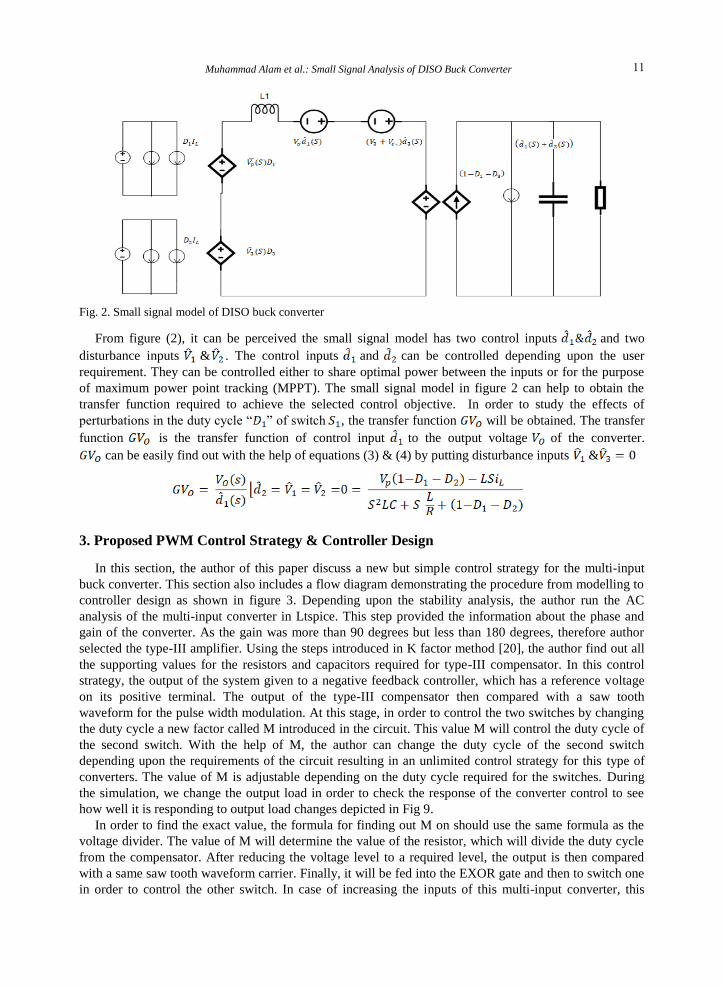
Fig. 2. Small signal model of DISO buck converter
From figure (2), it can be perceived the small signal model has two control inputs and two
disturbance inputs & . The control inputs and can be controlled depending upon the user
requirement. They can be controlled either to share optimal power between the inputs or for the purpose
of maximum power point tracking (MPPT). The small signal model in figure 2 can help to obtain the
transfer function required to achieve the selected control objective. In order to study the effects of
perturbations in the duty cycle “ ” of switch , the transfer function will be obtained. The transfer
function is the transfer function of control input to the output voltage of the converter.
can be easily find out with the help of equations (3) & (4) by putting disturbance inputs &
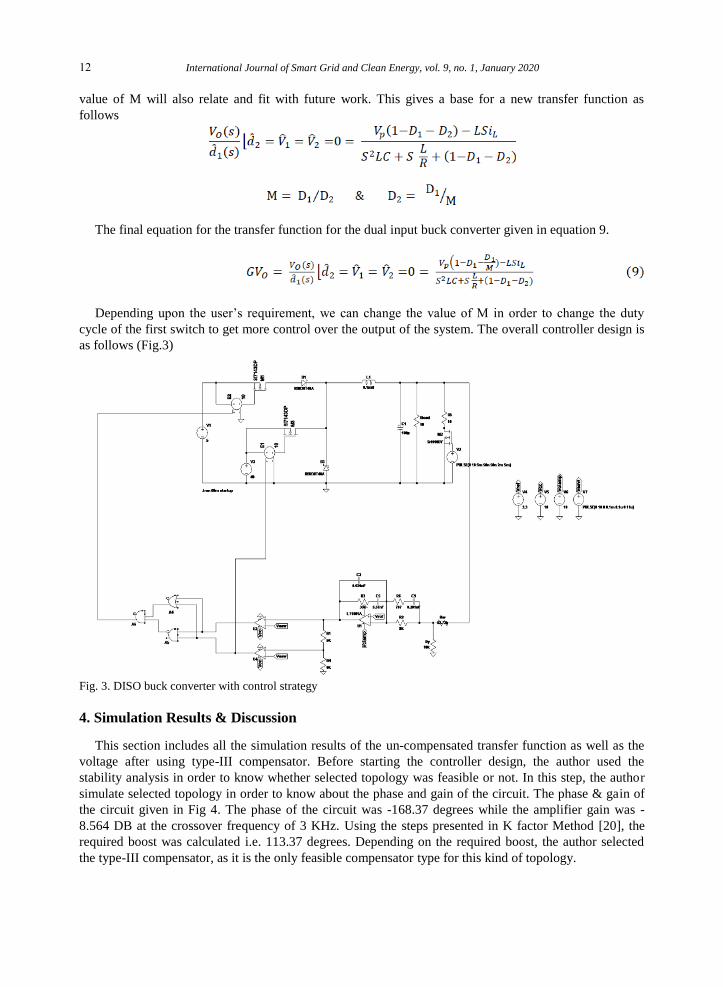
3. Proposed PWM Control Strategy & Controller Design
In this section, the author of this paper discuss a new but simple control strategy for the multi-input
buck converter. This section also includes a flow diagram demonstrating the procedure from modelling to
controller design as shown in figure 3. Depending upon the stability analysis, the author run the AC
analysis of the multi-input converter in Ltspice. This step provided the information about the phase and
gain of the converter. As the gain was more than 90 degrees but less than 180 degrees, therefore author
selected the type-III amplifier. Using the steps introduced in K factor method [20], the author find out all
the supporting values for the resistors and capacitors required for type-III compensator. In this control
strategy, the output of the system given to a negative feedback controller, which has a reference voltage
on its positive terminal. The output of the type-III compensator then compared with a saw tooth
waveform for the pulse width modulation. At this stage, in order to control the two switches by changing
the duty cycle a new factor called M introduced in the circuit. This value M will control the duty cycle of
the second switch. With the help of M, the author can change the duty cycle of the second switch
depending upon the requirements of the circuit resulting in an unlimited control strategy for this type of
converters. The value of M is adjustable depending on the duty cycle required for the switches. During
the simulation, we change the output load in order to check the response of the converter control to see
how well it is responding to output load changes depicted in Fig 9.
In order to find the exact value, the formula for finding out M on should use the same formula as the
voltage divider. The value of M will determine the value of the resistor, which will divide the duty cycle
from the compensator. After reducing the voltage level to a required level, the output is then compared
with a same saw tooth waveform carrier. Finally, it will be fed into the EXOR gate and then to switch one
in order to control the other switch. In case of increasing the inputs of this multi-input converter, this
11Muhammad Alam et al.: Small Signal Analysis of DISO Buck Converter
value of M will also relate and fit with future work. This gives a base for a new transfer function as
follows
The final equation for the transfer function for the dual input buck converter given in equation 9.
Depending upon the user’s requirement, we can change the value of M in order to change the duty
cycle of the first switch to get more control over the output of the system. The overall controller design is
as follows (Fig.3)
Fig. 3. DISO buck converter with control strategy
4. Simulation Results & Discussion
This section includes all the simulation results of the un-compensated transfer function as well as the
voltage after using type-III compensator. Before starting the controller design, the author used the
stability analysis in order to know whether selected topology was feasible or not. In this step, the author
simulate selected topology in order to know about the phase and gain of the circuit. The phase & gain of
the circuit given in Fig 4. The phase of the circuit was -168.37 degrees while the amplifier gain was -
8.564 DB at the crossover frequency of 3 KHz. Using the steps presented in K factor Method [20], the
required boost was calculated i.e. 113.37 degrees. Depending on the required boost, the author selected
the type-III compensator, as it is the only feasible compensator type for this kind of topology.
12 International Journal of Smart Grid and Clean Energy, vol. 9 , no. 1, January 2020
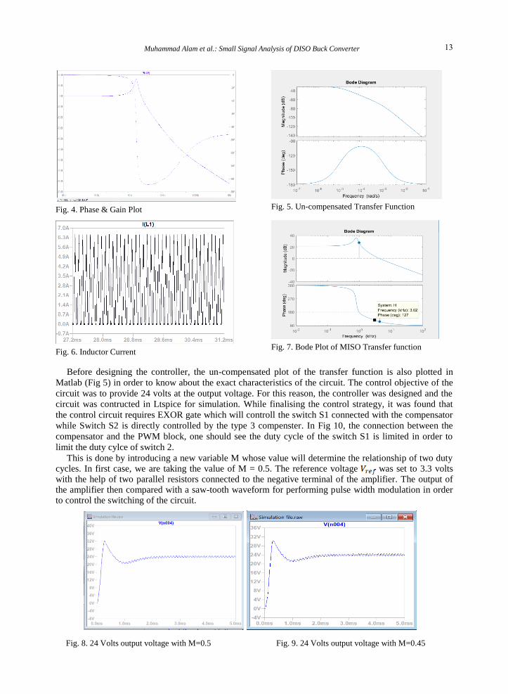
Fig. 4. Phase & Gain Plot
Fig. 5. Un-compensated Transfer Function
Fig. 6. Inductor Current
Fig. 7. Bode Plot of MISO Transfer function
Before designing the controller, the un-compensated plot of the transfer function is also plotted in
Matlab (Fig 5) in order to know about the exact characteristics of the circuit. The control objective of the
circuit was to provide 24 volts at the output voltage. For this reason, the controller was designed and the
circuit was contructed in Ltspice for simulation. While finalising the control strategy, it was found that
the control circuit requires EXOR gate which will controll the switch S1 connected with the compensator
while Switch S2 is directly controlled by the type 3 compenster. In Fig 10, the connection between the
compensator and the PWM block, one should see the duty cycle of the switch S1 is limited in order to
limit the duty cylce of switch 2.
This is done by introducing a new variable M whose value will determine the relationship of two duty cycles. In first case, we are taking the value of M = 0.5. The reference voltage was set to 3.3 volts with the help of two parallel resistors connected to the negative terminal of the amplifier. The output of the amplifier then compared with a saw-tooth waveform for performing pulse width modulation in order to control the switching of the circuit.
Fig. 8. 24 Volts output voltage with M=0.5 Fig. 9. 24 Volts output voltage with M=0.45
13Muhammad Alam et al.: Small Signal Analysis of DISO Buck Converter
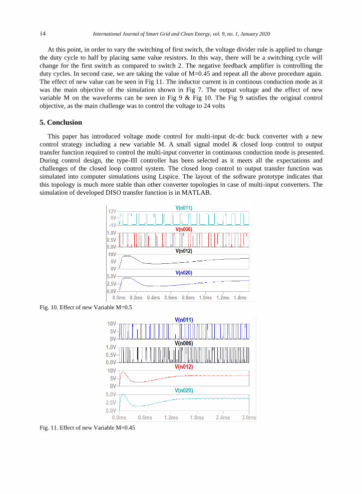
At this point, in order to vary the switching of first switch, the voltage divider rule is applied to change
the duty cycle to half by placing same value resistors. In this way, there will be a switching cycle will
change for the first switch as compared to switch 2. The negative feedback amplifier is controlling the
duty cycles. In second case, we are taking the value of M=0.45 and repeat all the above procedure again.
The effect of new value can be seen in Fig 11. The inductor current is in continous conduction mode as it
was the main objective of the simulation shown in Fig 7. The output voltage and the effect of new
variable M on the waveforms can be seen in Fig 9 & Fig 10. The Fig 9 satisfies the original control
objective, as the main challenge was to control the voltage to 24 volts
5. Conclusion
This paper has introduced voltage mode control for multi-input dc-dc buck converter with a new
control strategy including a new variable M. A small signal model & closed loop control to output
transfer function required to control the multi-input converter in continuous conduction mode is presented.
During control design, the type-III controller has been selected as it meets all the expectations and
challenges of the closed loop control system. The closed loop control to output transfer function was
simulated into computer simulations using Ltspice. The layout of the software prototype indicates that
this topology is much more stable than other converter topologies in case of multi-input converters. The
simulation of developed DISO transfer function is in MATLAB.
Fig. 10. Effect of new Variable M=0.5
Fig. 11. Effect of new Variable M=0.45
14 International Journal of Smart Grid and Clean Energy, vol. 9 , no. 1, January 2020
Conflict of Interest
The authors declare no conflict of Interest.
Author Contributions
This paper is contributed by three different authors. M M Alam (Author A) has prepared the small
signal modelling of the DISO Buck converter. The author A went through a number of steps while
completing this stage. It includes gathering all knowledge about mathematical steps involved in the
calculations, cross-checking the results with the theoretical knowledge. The author A also finished the
simulation part of the work where he went through a number of problems. At the end, the author A wrote
the paper. During this whole procedure, the D C Lu (Author B) and Y Siwakoti (Author C) were
supervising Author A. Whenever any problem arises during calculations, writing or simulation, the
Author B and C helped Author A. Finally, all the results were double checked by the Author B and C.
Author B and C also done the cross check of paper writing and provided help in the simulation of the idea.
At the end, all the authors had found the final draft complete and ready for publishing.
Acknowledgement
We would like to thanks Australian Government Training & Scholarship program (RTP) who fully
supports this research.
References
[1] Krishna KS and Kumar KS. A review on hybrid renewable energy systems. Renewable and Sustainable Energy Reviews, 2015;
52: 907-916.
[2] Reza C, Lu DDC, and Qin L. Single-inductor multiple-source mixer for DC power packet dispatching system. In: Proc. of
2017 IEEE Second International Conference on DC Microgrids (ICDCM), 2017; 553-557.
[3] Somayajula D and Ferdowsi M. Small-signal modeling and analysis of the double-input buckboost converter. In: Proc. of 2010
Twenty-Fifth Annual IEEE Conference on Applied Power Electronics and Exposition (APEC)., 2010; 2111-2115.
[4] Benavides ND and Chapman PL. Power budgeting of a multiple-input buck-boost converter. IEEE Transactions on Power
Electronics, 2005; 20(6): 1303-1309.
[5] Prabhala VAK, Khazraei M, and Ferdowsi M. A new control strategy for a class of multiple-input DC-DC converters. In: Proc.
of 2014 International Conference on Renewable Energy Research and Application (ICRERA), 2014; 508-513.
[6] Yalamanchili KP and Ferdowsi M. Review of multiple input DC-DC converters for electric and hybrid vehicles. In: Proc. of
2005 IEEE Vehicle Power and Propulsion Conference.
[7] Gummi K and Ferdowsi M. Synthesis of double-input dc-dc converters using a single-pole triple-throw switch as a building
block. In: Proc. of IEEE Conference on Power Electronics Specialists, 2008; 2819-2823.
[8] Dobbs BG and Chapman PL. A multiple-input DC-DC converter topology. IEEE Power Electronics Letters, 2003; 1(1); 6-9.
[9] Choung SH and Kwasinski A. Multiple-input DC-DC converter topologies comparison. in Industrial Electronics, IECON
2008. 34th Annual Conference of IEEE, 2008; 2359-2364.
[10] Chen YM, Liu YC, and Lin SH. Double-input PWM DC/DC converter for high-/low-voltage sources. IEEE Transactions on
Industrial Electronics. 2006; 53(5): 1538-1545.
[11] Yang D, Yang M, and Ruan X. One-cycle control for a double-input DC/DC converter. IEEE Transactions on Power
Electronics, 2012; 27(11): 4646-4655.
[12] Xian L, Wang G, and Wang Y. Subproportion control of double input buck converter for fuel cell/battery hybrid power supply
system. IET Power Electronics, 2014; 7(8): 2141-2150.
[13] Prabhala VAK. Control and applications of double input DC-DC power electronic converters. Master Thesis no 9681,
Missouri University of Science & Technology, 2010.
[14] Nejabatkhah F, Danyali S, Hosseini SH, Sabahi M, and Niapour SM. Modeling and control of a new three-input DC–DC boost
converter for hybrid PV/FC/battery power system. IEEE Transactions on Power Electronics, 2012; 27(5): 2309-2324.
[15] Prabhala VAK, Somayajula D, and Ferdowsi M. Power sharing in a double-input buck converter using dead-time control. In:
Proc. of IEEE Conference on Energy Conversion Congress and Exposition, 2009: 2621-2626.
[16] Somayajula D and Ferdowsi M. Small-signal modeling and analysis of the double-input Buckboost converter. 2010 Twenty-
15Muhammad Alam et al.: Small Signal Analysis of DISO Buck Converter

Fifth Annual IEEE Applied Power Electronics Conference and Exposition (APEC).
[17] Zhang Z, Thomsen OC, and Andersen MA. Modeling and control of a dual-Input isolated full-bridge boost converter. In: Proc.
Applied Power Electronics Conference and Exposition (APEC), 2012 Twenty-Seventh Annual IEEE, 2012; 2017-2023.
[18] González A, López-Erauskin R, and Gyselinck J. Interleaved three-port boost converter for photovoltaic systems including
storage. In: Proc. of 2017 19th European Conference on Power Electronics and Applications (EPE'17 ECCE Europe), , 2017,
pp. P. 1-P. 9.
[19] Mathews BM and Barai M. A synchronized voltage-mode control for a multi-port dc-dc converter. In: Proc. of 2016 IEEE
International Conference on Power Electronics, Drives and Energy Systems (PEDES), , 2016: 1-6.
[20] Venable HD. The K factor: A new mathematical tool for stability analysis and synthesis. In: Proc. Powercon, 1983; 10: H1-1.
[21] Kassakian JG, Schlecht MF, and Verghese GC. Principles of Power Electronics, Graphis, 2000.
[22] Maksimovic D and Erickson RW. Fundamentals of power electronics, Norwell, MA, Kluwer Academic Publish-ers, 2001.
Copyright © 2020 by the authors. This is an open access article distributed under the Creative Commons Attribution License (CC
BY-NC-ND 4.0), which permits use, distribution and reproduction in any medium, provided that the article is properly cited, the use
is non-commercial and no modifications or adaptations are made.
16 International Journal of Smart Grid and Clean Energy, vol. 9 , no. 1, January 2020