Embed Size (px)
Citation preview
LM117, LM317-N
www.ti.com SNVS774L –MAY 2004–REVISED FEBRUARY 2011
LM117/LM317A/LM317-N 3-Terminal Adjustable RegulatorCheck for Samples: LM117, LM317-N
Normally, no capacitors are needed unless the device1FEATURES
is situated more than 6 inches from the input filter2• Specified 1% Output Voltage Tolerance capacitors in which case an input bypass is needed.
(LM317A) An optional output capacitor can be added to improve• Specified Max. 0.01%/V Line Regulation transient response. The adjustment terminal can be
bypassed to achieve very high ripple rejection ratios(LM317A)which are difficult to achieve with standard 3-terminal• Specified Max. 0.3% Load Regulation (LM117)regulators.
• Specified 1.5A Output CurrentBesides replacing fixed regulators, the LM117 is• Adjustable Output Down to 1.2Vuseful in a wide variety of other applications. Since
• Current Limit Constant With Temperature the regulator is “floating” and sees only the input-to-output differential voltage, supplies of several• P+ Product Enhancement Testedhundred volts can be regulated as long as the• 80 dB Ripple Rejectionmaximum input to output differential is not exceeded,
• Output is Short-Circuit Protected i.e., avoid short-circuiting the output.
Also, it makes an especially simple adjustableDESCRIPTIONswitching regulator, a programmable output regulator,
The LM117 series of adjustable 3-terminal positive or by connecting a fixed resistor between thevoltage regulators is capable of supplying in excess adjustment pin and output, the LM117 can be usedof 1.5A over a 1.2V to 37V output range. They are as a precision current regulator. Supplies withexceptionally easy to use and require only two electronic shutdown can be achieved by clamping theexternal resistors to set the output voltage. Further, adjustment terminal to ground which programs theboth line and load regulation are better than standard output to 1.2V where most loads draw little current.fixed regulators. Also, the LM117 is packaged instandard transistor packages which are easily For applications requiring greater output current, seemounted and handled. LM150 series (3A) and LM138 series (5A) data
sheets. For the negative complement, see LM137In addition to higher performance than fixed series data sheet.regulators, the LM117 series offers full overloadprotection available only in IC's. Included on the chipare current limit, thermal overload protection and safearea protection. All overload protection circuitryremains fully functional even if the adjustmentterminal is disconnected.
1
Please be aware that an important notice concerning availability, standard warranty, and use in critical applications ofTexas Instruments semiconductor products and disclaimers thereto appears at the end of this data sheet.
2All trademarks are the property of their respective owners.
PRODUCTION DATA information is current as of publication date. Copyright © 2004–2011, Texas Instruments IncorporatedProducts conform to specifications per the terms of the TexasInstruments standard warranty. Production processing does notnecessarily include testing of all parameters.
LM117, LM317-N
SNVS774L –MAY 2004–REVISED FEBRUARY 2011 www.ti.com
Typical Applications
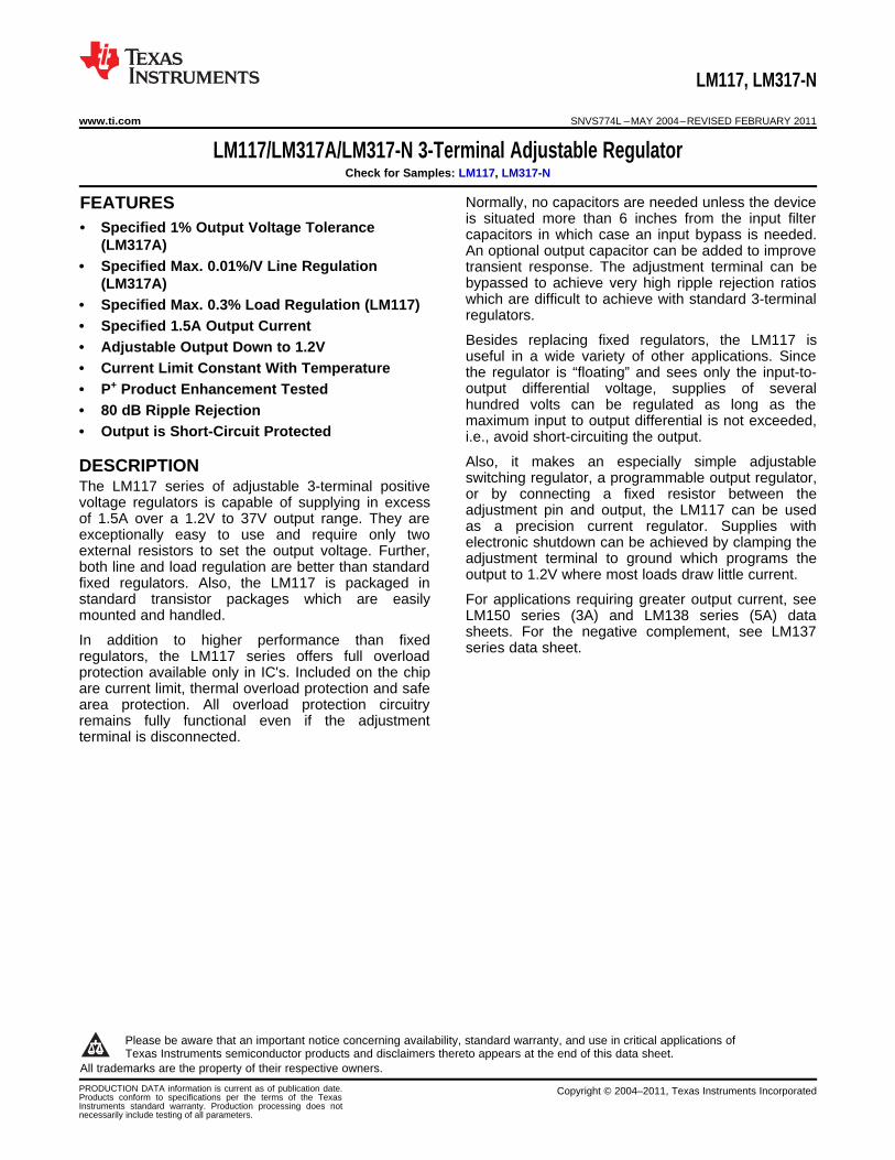
Figure 1. 1.2V–25V Adjustable Regulator LM117/LM317A/LM317-N Package OptionsOutputPart Number Suffix Package Current
LM117, LM317-N NDS TO-3 1.5A
LM317A, LM317-N NDE TO-220 1.5A
LM317-N KTT TO-263 1.5A
LM317A, LM317-N DCY SOT-223 1.0A
LM117, LM317A, LM317-N NDT TO 0.5A
LM117 NAJ LCCC 0.5A
LM317A, LM317-N NDP PFM 0.5A
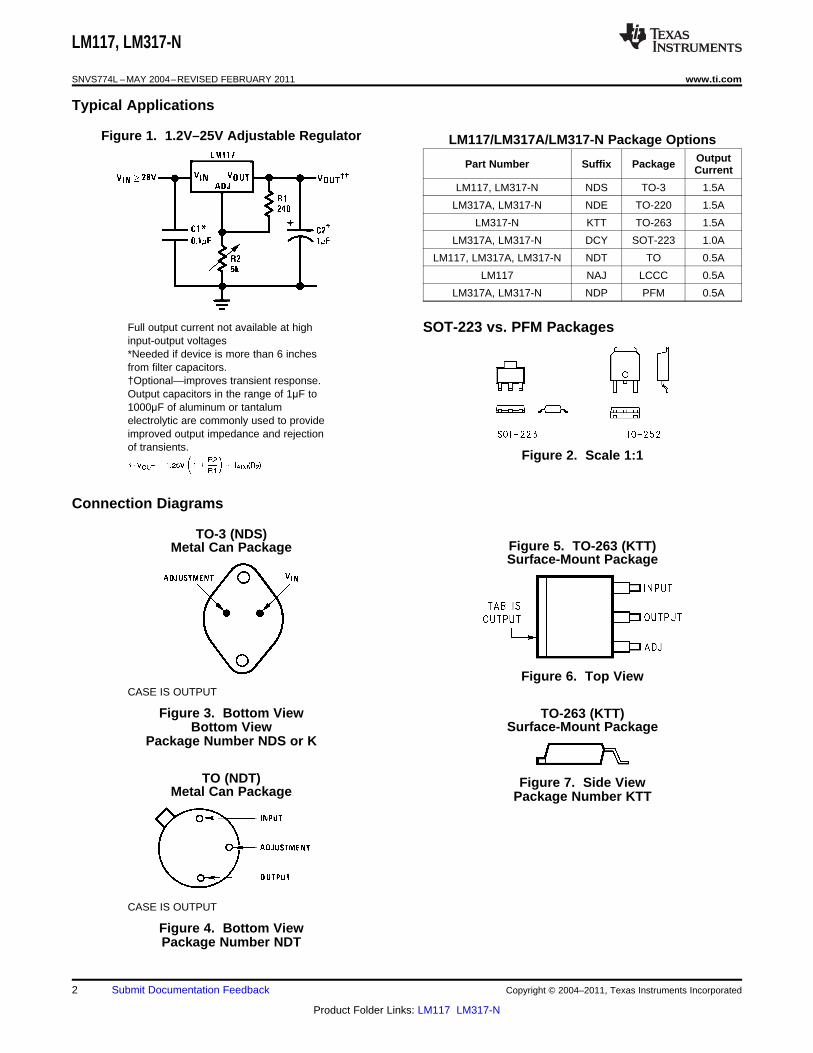
Full output current not available at high SOT-223 vs. PFM Packagesinput-output voltages*Needed if device is more than 6 inchesfrom filter capacitors.†Optional—improves transient response.Output capacitors in the range of 1μF to1000μF of aluminum or tantalumelectrolytic are commonly used to provideimproved output impedance and rejectionof transients.
Figure 2. Scale 1:1
Connection Diagrams
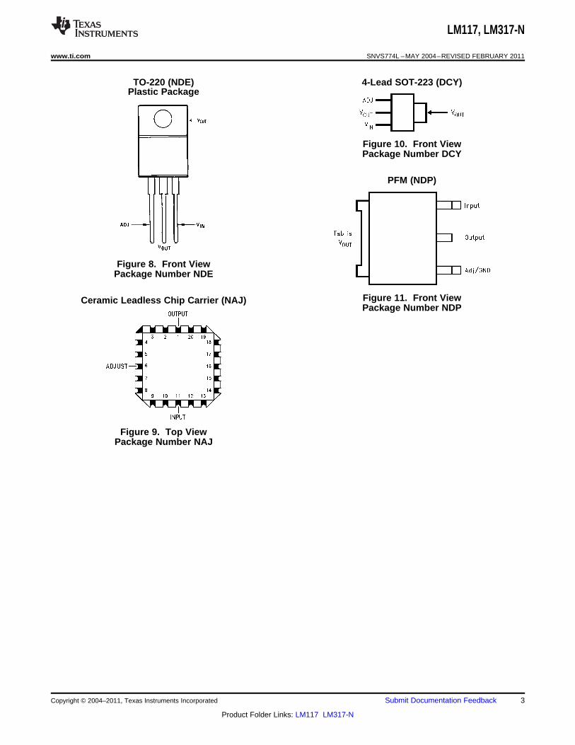
TO-3 (NDS)Figure 5. TO-263 (KTT)Metal Can PackageSurface-Mount Package
Figure 6. Top ViewCASE IS OUTPUT
Figure 3. Bottom View TO-263 (KTT)Surface-Mount PackageBottom View
Package Number NDS or K
TO (NDT) Figure 7. Side ViewMetal Can Package Package Number KTT
CASE IS OUTPUT
Figure 4. Bottom ViewPackage Number NDT
2 Submit Documentation Feedback Copyright © 2004–2011, Texas Instruments Incorporated
Product Folder Links: LM117 LM317-N
LM117, LM317-N
www.ti.com SNVS774L –MAY 2004–REVISED FEBRUARY 2011
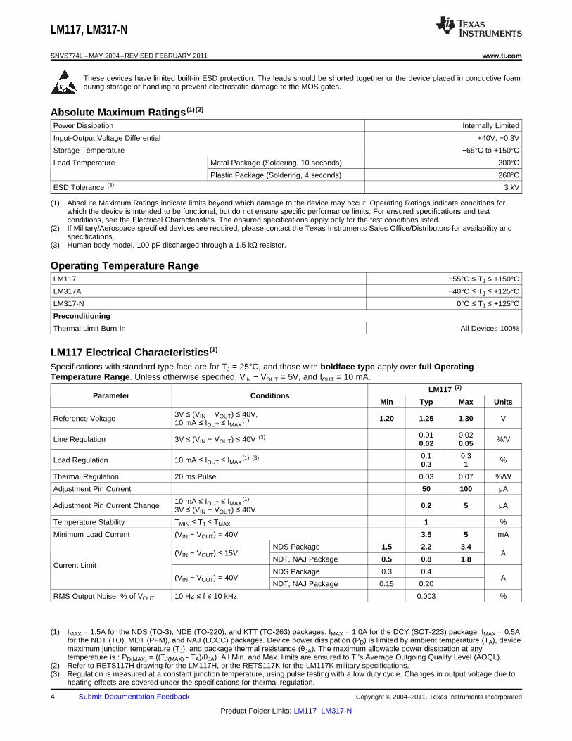
TO-220 (NDE) 4-Lead SOT-223 (DCY)Plastic Package
Figure 10. Front ViewPackage Number DCY
PFM (NDP)
Figure 8. Front ViewPackage Number NDE
Figure 11. Front ViewCeramic Leadless Chip Carrier (NAJ)Package Number NDP
Figure 9. Top ViewPackage Number NAJ
Copyright © 2004–2011, Texas Instruments Incorporated Submit Documentation Feedback 3
Product Folder Links: LM117 LM317-N
LM117, LM317-N
SNVS774L –MAY 2004–REVISED FEBRUARY 2011 www.ti.com
These devices have limited built-in ESD protection. The leads should be shorted together or the device placed in conductive foamduring storage or handling to prevent electrostatic damage to the MOS gates.
Absolute Maximum Ratings (1) (2)
Power Dissipation Internally Limited
Input-Output Voltage Differential +40V, −0.3V
Storage Temperature −65°C to +150°C
Lead Temperature Metal Package (Soldering, 10 seconds) 300°C
Plastic Package (Soldering, 4 seconds) 260°C
ESD Tolerance (3) 3 kV
(1) Absolute Maximum Ratings indicate limits beyond which damage to the device may occur. Operating Ratings indicate conditions forwhich the device is intended to be functional, but do not ensure specific performance limits. For ensured specifications and testconditions, see the Electrical Characteristics. The ensured specifications apply only for the test conditions listed.
(2) If Military/Aerospace specified devices are required, please contact the Texas Instruments Sales Office/Distributors for availability andspecifications.
(3) Human body model, 100 pF discharged through a 1.5 kΩ resistor.
Operating Temperature RangeLM117 −55°C ≤ TJ ≤ +150°C
LM317A −40°C ≤ TJ ≤ +125°C
LM317-N 0°C ≤ TJ ≤ +125°C
Preconditioning
Thermal Limit Burn-In All Devices 100%
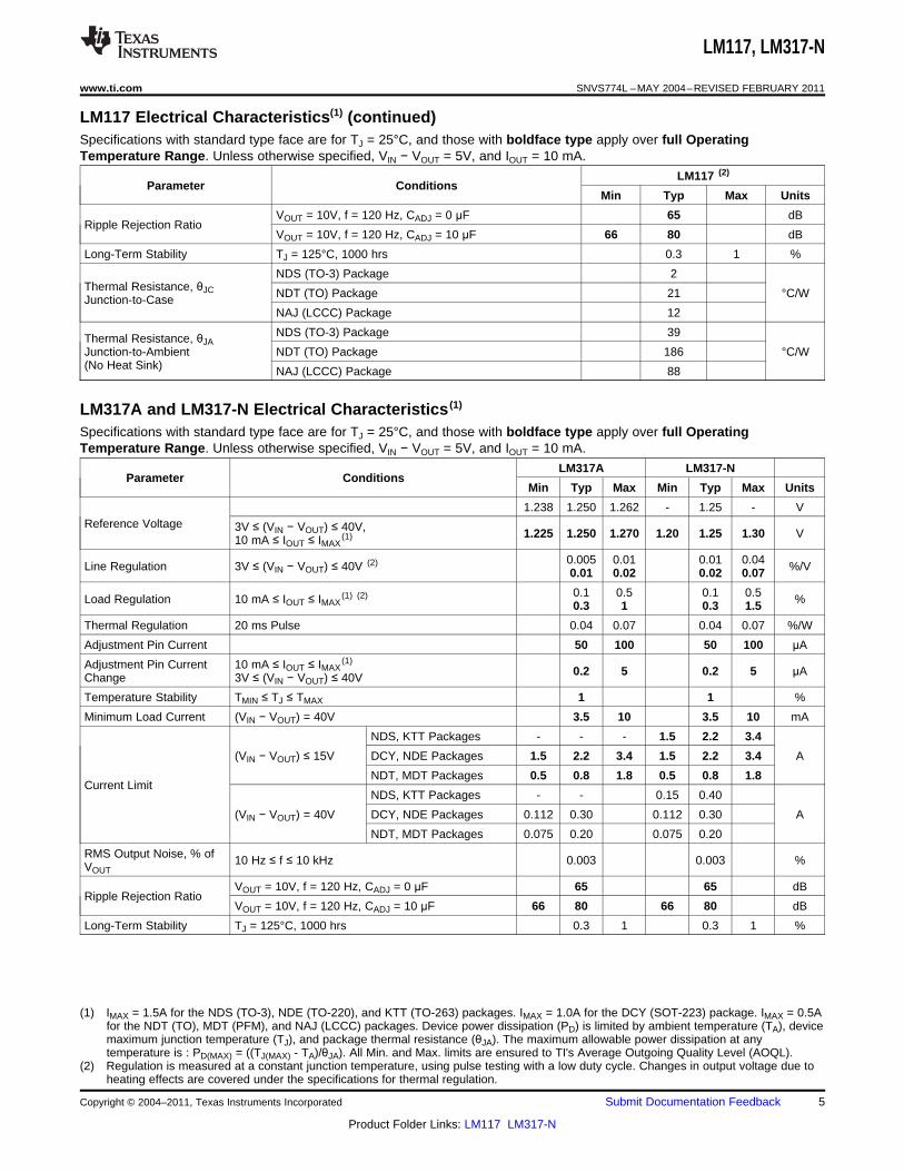
LM117 Electrical Characteristics (1)
Specifications with standard type face are for TJ = 25°C, and those with boldface type apply over full OperatingTemperature Range. Unless otherwise specified, VIN − VOUT = 5V, and IOUT = 10 mA.
LM117 (2)
Parameter ConditionsMin Typ Max Units
3V ≤ (VIN − VOUT) ≤ 40V,Reference Voltage 1.20 1.25 1.30 V10 mA ≤ IOUT ≤ IMAX(1)
0.01 0.02Line Regulation 3V ≤ (VIN − VOUT) ≤ 40V (3) %/V0.02 0.05
0.1 0.3Load Regulation 10 mA ≤ IOUT ≤ IMAX(1) (3) %0.3 1
Thermal Regulation 20 ms Pulse 0.03 0.07 %/W
Adjustment Pin Current 50 100 μA
10 mA ≤ IOUT ≤ IMAX(1)
Adjustment Pin Current Change 0.2 5 μA3V ≤ (VIN − VOUT) ≤ 40V
Temperature Stability TMIN ≤ TJ ≤ TMAX 1 %
Minimum Load Current (VIN − VOUT) = 40V 3.5 5 mA
NDS Package 1.5 2.2 3.4(VIN − VOUT) ≤ 15V A
NDT, NAJ Package 0.5 0.8 1.8Current Limit
NDS Package 0.3 0.4(VIN − VOUT) = 40V A
NDT, NAJ Package 0.15 0.20
RMS Output Noise, % of VOUT 10 Hz ≤ f ≤ 10 kHz 0.003 %
(1) IMAX = 1.5A for the NDS (TO-3), NDE (TO-220), and KTT (TO-263) packages. IMAX = 1.0A for the DCY (SOT-223) package. IMAX = 0.5Afor the NDT (TO), MDT (PFM), and NAJ (LCCC) packages. Device power dissipation (PD) is limited by ambient temperature (TA), devicemaximum junction temperature (TJ), and package thermal resistance (θJA). The maximum allowable power dissipation at anytemperature is : PD(MAX) = ((TJ(MAX) - TA)/θJA). All Min. and Max. limits are ensured to TI's Average Outgoing Quality Level (AOQL).
(2) Refer to RETS117H drawing for the LM117H, or the RETS117K for the LM117K military specifications.(3) Regulation is measured at a constant junction temperature, using pulse testing with a low duty cycle. Changes in output voltage due to
heating effects are covered under the specifications for thermal regulation.
4 Submit Documentation Feedback Copyright © 2004–2011, Texas Instruments Incorporated
Product Folder Links: LM117 LM317-N
LM117, LM317-N
www.ti.com SNVS774L –MAY 2004–REVISED FEBRUARY 2011
LM117 Electrical Characteristics(1) (continued)Specifications with standard type face are for TJ = 25°C, and those with boldface type apply over full OperatingTemperature Range. Unless otherwise specified, VIN − VOUT = 5V, and IOUT = 10 mA.
LM117 (2)
Parameter ConditionsMin Typ Max Units
VOUT = 10V, f = 120 Hz, CADJ = 0 μF 65 dBRipple Rejection Ratio
VOUT = 10V, f = 120 Hz, CADJ = 10 μF 66 80 dB
Long-Term Stability TJ = 125°C, 1000 hrs 0.3 1 %
NDS (TO-3) Package 2Thermal Resistance, θJC NDT (TO) Package 21 °C/WJunction-to-Case
NAJ (LCCC) Package 12
NDS (TO-3) Package 39Thermal Resistance, θJAJunction-to-Ambient NDT (TO) Package 186 °C/W(No Heat Sink) NAJ (LCCC) Package 88
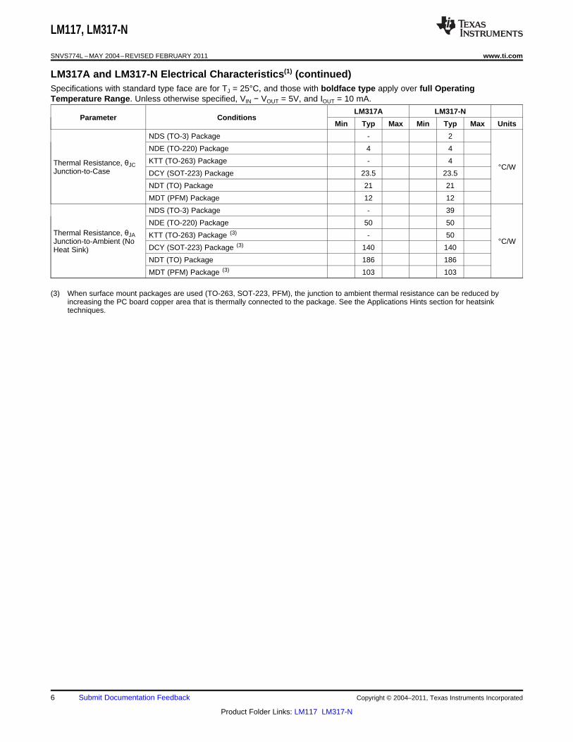
LM317A and LM317-N Electrical Characteristics (1)
Specifications with standard type face are for TJ = 25°C, and those with boldface type apply over full OperatingTemperature Range. Unless otherwise specified, VIN − VOUT = 5V, and IOUT = 10 mA.
LM317A LM317-NParameter Conditions
Min Typ Max Min Typ Max Units
1.238 1.250 1.262 - 1.25 - VReference Voltage 3V ≤ (VIN − VOUT) ≤ 40V, 1.225 1.250 1.270 1.20 1.25 1.30 V10 mA ≤ IOUT ≤ IMAX
(1)
0.005 0.01 0.01 0.04Line Regulation 3V ≤ (VIN − VOUT) ≤ 40V (2) %/V0.01 0.02 0.02 0.07
0.1 0.5 0.1 0.5Load Regulation 10 mA ≤ IOUT ≤ IMAX(1) (2) %0.3 1 0.3 1.5
Thermal Regulation 20 ms Pulse 0.04 0.07 0.04 0.07 %/W
Adjustment Pin Current 50 100 50 100 μA
Adjustment Pin Current 10 mA ≤ IOUT ≤ IMAX(1)
0.2 5 0.2 5 μAChange 3V ≤ (VIN − VOUT) ≤ 40V
Temperature Stability TMIN ≤ TJ ≤ TMAX 1 1 %
Minimum Load Current (VIN − VOUT) = 40V 3.5 10 3.5 10 mA
NDS, KTT Packages - - - 1.5 2.2 3.4
(VIN − VOUT) ≤ 15V DCY, NDE Packages 1.5 2.2 3.4 1.5 2.2 3.4 A
NDT, MDT Packages 0.5 0.8 1.8 0.5 0.8 1.8Current Limit
NDS, KTT Packages - - 0.15 0.40
(VIN − VOUT) = 40V DCY, NDE Packages 0.112 0.30 0.112 0.30 A
NDT, MDT Packages 0.075 0.20 0.075 0.20
RMS Output Noise, % of 10 Hz ≤ f ≤ 10 kHz 0.003 0.003 %VOUT
VOUT = 10V, f = 120 Hz, CADJ = 0 μF 65 65 dBRipple Rejection Ratio
VOUT = 10V, f = 120 Hz, CADJ = 10 μF 66 80 66 80 dB
Long-Term Stability TJ = 125°C, 1000 hrs 0.3 1 0.3 1 %
(1) IMAX = 1.5A for the NDS (TO-3), NDE (TO-220), and KTT (TO-263) packages. IMAX = 1.0A for the DCY (SOT-223) package. IMAX = 0.5Afor the NDT (TO), MDT (PFM), and NAJ (LCCC) packages. Device power dissipation (PD) is limited by ambient temperature (TA), devicemaximum junction temperature (TJ), and package thermal resistance (θJA). The maximum allowable power dissipation at anytemperature is : PD(MAX) = ((TJ(MAX) - TA)/θJA). All Min. and Max. limits are ensured to TI's Average Outgoing Quality Level (AOQL).
(2) Regulation is measured at a constant junction temperature, using pulse testing with a low duty cycle. Changes in output voltage due toheating effects are covered under the specifications for thermal regulation.
Copyright © 2004–2011, Texas Instruments Incorporated Submit Documentation Feedback 5
Product Folder Links: LM117 LM317-N
LM117, LM317-N
SNVS774L –MAY 2004–REVISED FEBRUARY 2011 www.ti.com
LM317A and LM317-N Electrical Characteristics(1) (continued)Specifications with standard type face are for TJ = 25°C, and those with boldface type apply over full OperatingTemperature Range. Unless otherwise specified, VIN − VOUT = 5V, and IOUT = 10 mA.
LM317A LM317-NParameter Conditions
Min Typ Max Min Typ Max Units
NDS (TO-3) Package - 2
NDE (TO-220) Package 4 4
KTT (TO-263) Package - 4Thermal Resistance, θJC °C/WJunction-to-Case DCY (SOT-223) Package 23.5 23.5
NDT (TO) Package 21 21
MDT (PFM) Package 12 12
NDS (TO-3) Package - 39
NDE (TO-220) Package 50 50Thermal Resistance, θJA KTT (TO-263) Package (3) - 50Junction-to-Ambient (No °C/W
DCY (SOT-223) Package (3) 140 140Heat Sink)NDT (TO) Package 186 186
MDT (PFM) Package (3) 103 103
(3) When surface mount packages are used (TO-263, SOT-223, PFM), the junction to ambient thermal resistance can be reduced byincreasing the PC board copper area that is thermally connected to the package. See the Applications Hints section for heatsinktechniques.
6 Submit Documentation Feedback Copyright © 2004–2011, Texas Instruments Incorporated
Product Folder Links: LM117 LM317-N
LM117, LM317-N
www.ti.com SNVS774L –MAY 2004–REVISED FEBRUARY 2011
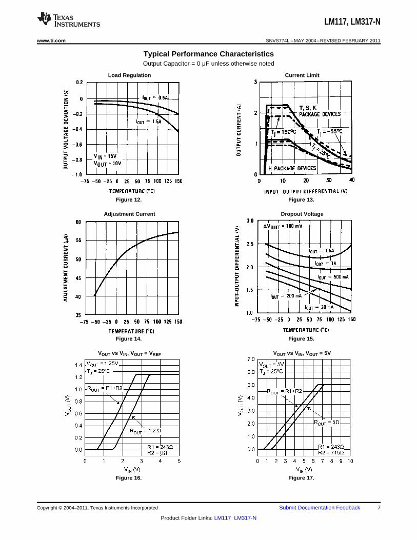
Typical Performance CharacteristicsOutput Capacitor = 0 μF unless otherwise noted
Load Regulation Current Limit
Figure 12. Figure 13.
Adjustment Current Dropout Voltage
Figure 14. Figure 15.
VOUT vs VIN, VOUT = VREF VOUT vs VIN, VOUT = 5V
Figure 16. Figure 17.
Copyright © 2004–2011, Texas Instruments Incorporated Submit Documentation Feedback 7
Product Folder Links: LM117 LM317-N
LM117, LM317-N
SNVS774L –MAY 2004–REVISED FEBRUARY 2011 www.ti.com
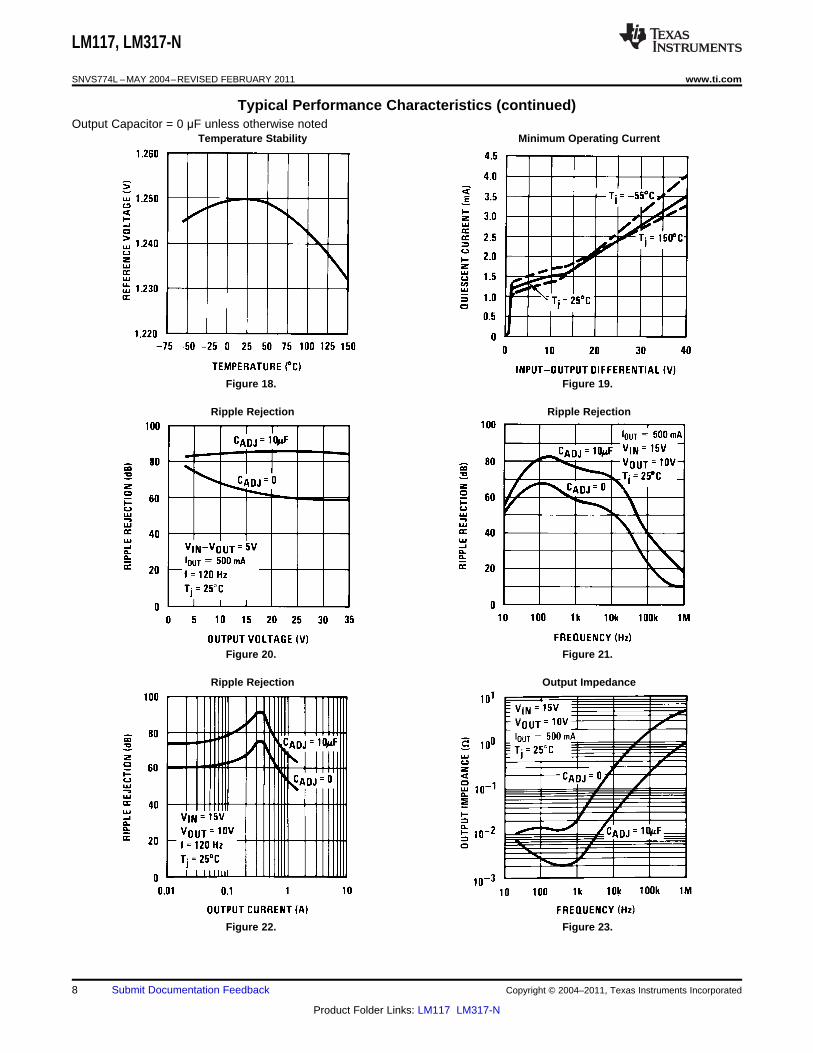
Typical Performance Characteristics (continued)Output Capacitor = 0 μF unless otherwise noted
Temperature Stability Minimum Operating Current
Figure 18. Figure 19.
Ripple Rejection Ripple Rejection
Figure 20. Figure 21.
Ripple Rejection Output Impedance
Figure 22. Figure 23.
8 Submit Documentation Feedback Copyright © 2004–2011, Texas Instruments Incorporated
Product Folder Links: LM117 LM317-N
LM117, LM317-N
www.ti.com SNVS774L –MAY 2004–REVISED FEBRUARY 2011
Typical Performance Characteristics (continued)Output Capacitor = 0 μF unless otherwise noted
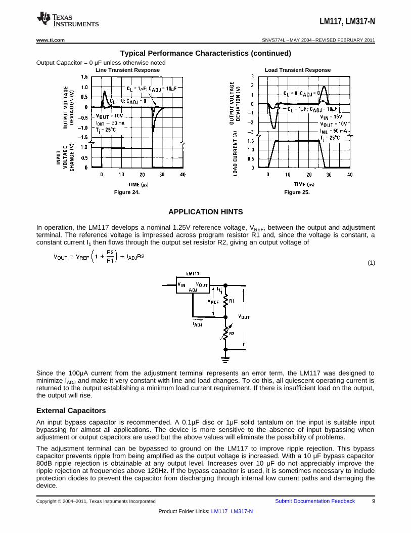
Line Transient Response Load Transient Response
Figure 24. Figure 25.
APPLICATION HINTS
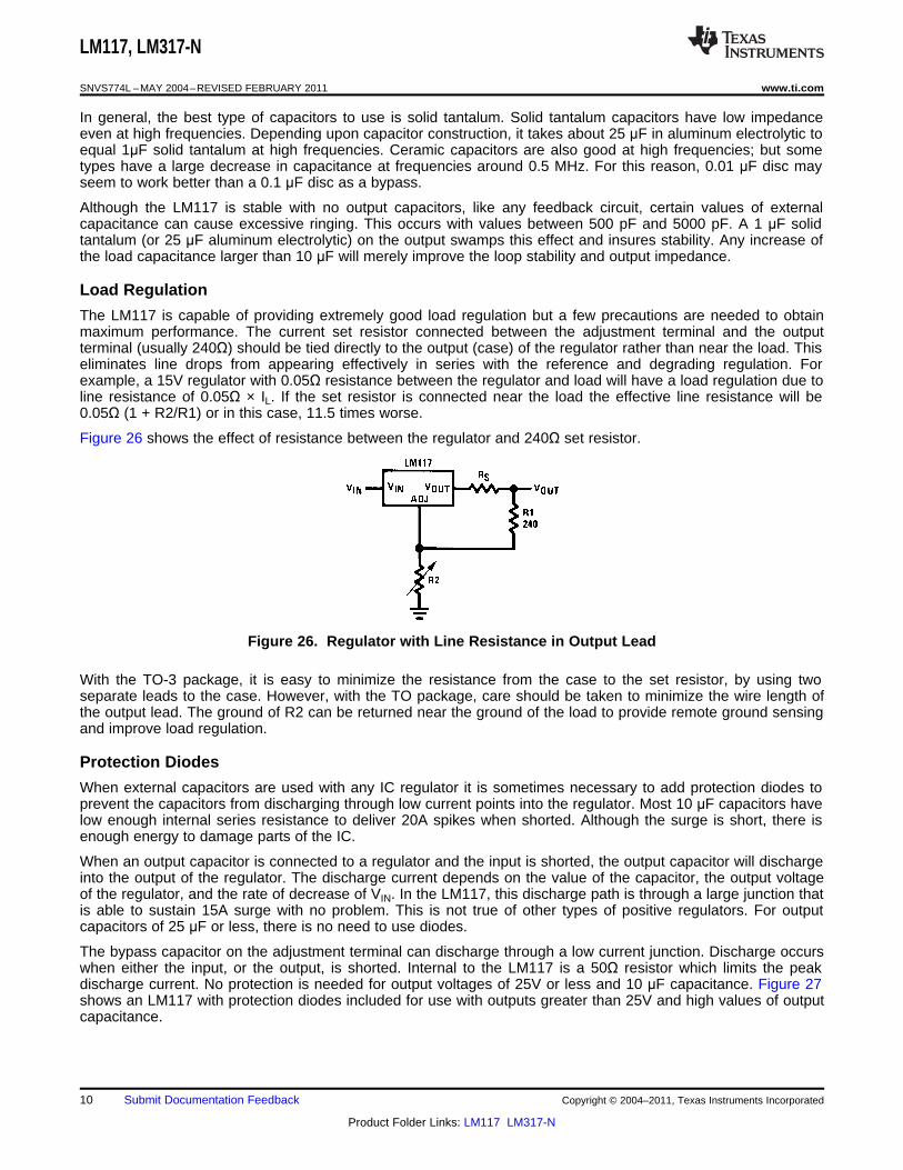
In operation, the LM117 develops a nominal 1.25V reference voltage, VREF, between the output and adjustmentterminal. The reference voltage is impressed across program resistor R1 and, since the voltage is constant, aconstant current I1 then flows through the output set resistor R2, giving an output voltage of
(1)
Since the 100μA current from the adjustment terminal represents an error term, the LM117 was designed tominimize IADJ and make it very constant with line and load changes. To do this, all quiescent operating current isreturned to the output establishing a minimum load current requirement. If there is insufficient load on the output,the output will rise.
External Capacitors
An input bypass capacitor is recommended. A 0.1μF disc or 1μF solid tantalum on the input is suitable inputbypassing for almost all applications. The device is more sensitive to the absence of input bypassing whenadjustment or output capacitors are used but the above values will eliminate the possibility of problems.
The adjustment terminal can be bypassed to ground on the LM117 to improve ripple rejection. This bypasscapacitor prevents ripple from being amplified as the output voltage is increased. With a 10 μF bypass capacitor80dB ripple rejection is obtainable at any output level. Increases over 10 μF do not appreciably improve theripple rejection at frequencies above 120Hz. If the bypass capacitor is used, it is sometimes necessary to includeprotection diodes to prevent the capacitor from discharging through internal low current paths and damaging thedevice.
Copyright © 2004–2011, Texas Instruments Incorporated Submit Documentation Feedback 9
Product Folder Links: LM117 LM317-N
LM117, LM317-N
SNVS774L –MAY 2004–REVISED FEBRUARY 2011 www.ti.com
In general, the best type of capacitors to use is solid tantalum. Solid tantalum capacitors have low impedanceeven at high frequencies. Depending upon capacitor construction, it takes about 25 μF in aluminum electrolytic toequal 1μF solid tantalum at high frequencies. Ceramic capacitors are also good at high frequencies; but sometypes have a large decrease in capacitance at frequencies around 0.5 MHz. For this reason, 0.01 μF disc mayseem to work better than a 0.1 μF disc as a bypass.
Although the LM117 is stable with no output capacitors, like any feedback circuit, certain values of externalcapacitance can cause excessive ringing. This occurs with values between 500 pF and 5000 pF. A 1 μF solidtantalum (or 25 μF aluminum electrolytic) on the output swamps this effect and insures stability. Any increase ofthe load capacitance larger than 10 μF will merely improve the loop stability and output impedance.
Load Regulation
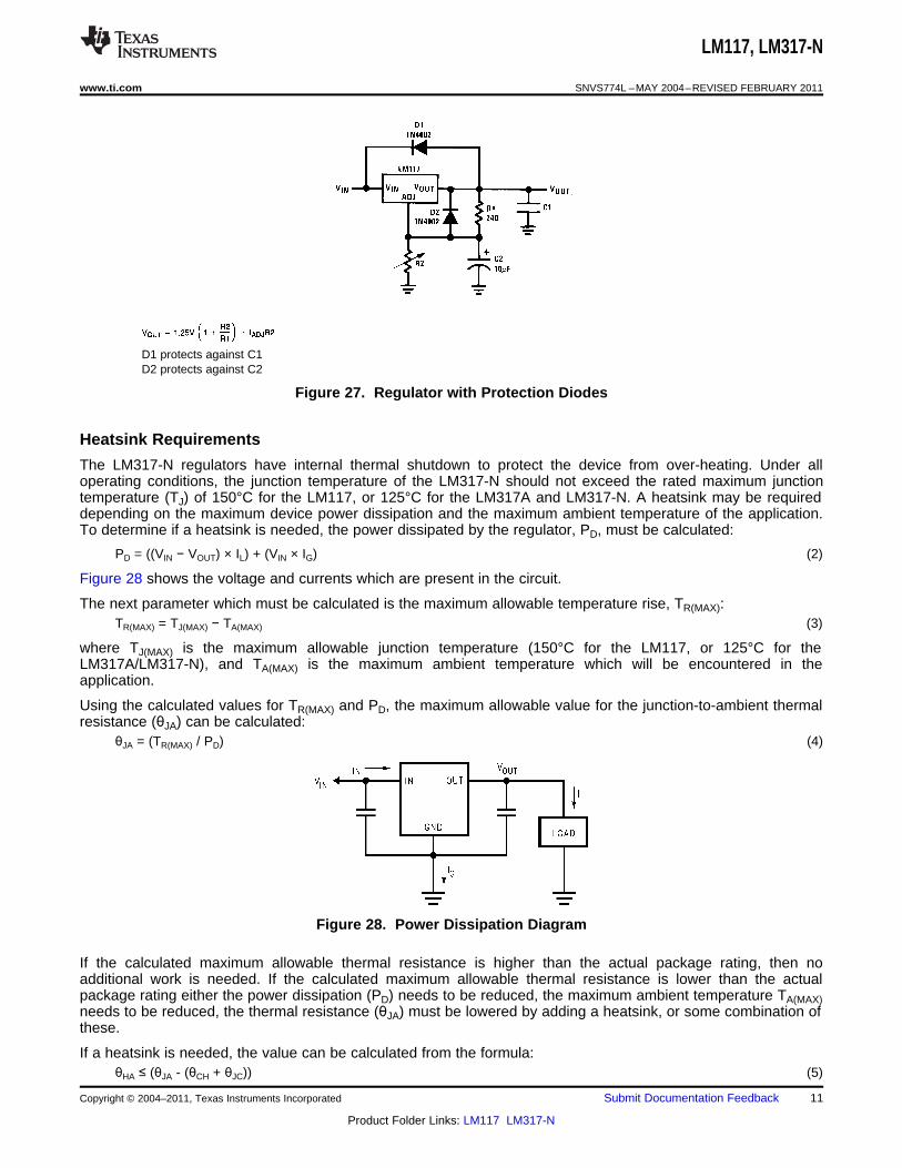
The LM117 is capable of providing extremely good load regulation but a few precautions are needed to obtainmaximum performance. The current set resistor connected between the adjustment terminal and the outputterminal (usually 240Ω) should be tied directly to the output (case) of the regulator rather than near the load. Thiseliminates line drops from appearing effectively in series with the reference and degrading regulation. Forexample, a 15V regulator with 0.05Ω resistance between the regulator and load will have a load regulation due toline resistance of 0.05Ω × IL. If the set resistor is connected near the load the effective line resistance will be0.05Ω (1 + R2/R1) or in this case, 11.5 times worse.
Figure 26 shows the effect of resistance between the regulator and 240Ω set resistor.
Figure 26. Regulator with Line Resistance in Output Lead
With the TO-3 package, it is easy to minimize the resistance from the case to the set resistor, by using twoseparate leads to the case. However, with the TO package, care should be taken to minimize the wire length ofthe output lead. The ground of R2 can be returned near the ground of the load to provide remote ground sensingand improve load regulation.
Protection Diodes
When external capacitors are used with any IC regulator it is sometimes necessary to add protection diodes toprevent the capacitors from discharging through low current points into the regulator. Most 10 μF capacitors havelow enough internal series resistance to deliver 20A spikes when shorted. Although the surge is short, there isenough energy to damage parts of the IC.
When an output capacitor is connected to a regulator and the input is shorted, the output capacitor will dischargeinto the output of the regulator. The discharge current depends on the value of the capacitor, the output voltageof the regulator, and the rate of decrease of VIN. In the LM117, this discharge path is through a large junction thatis able to sustain 15A surge with no problem. This is not true of other types of positive regulators. For outputcapacitors of 25 μF or less, there is no need to use diodes.
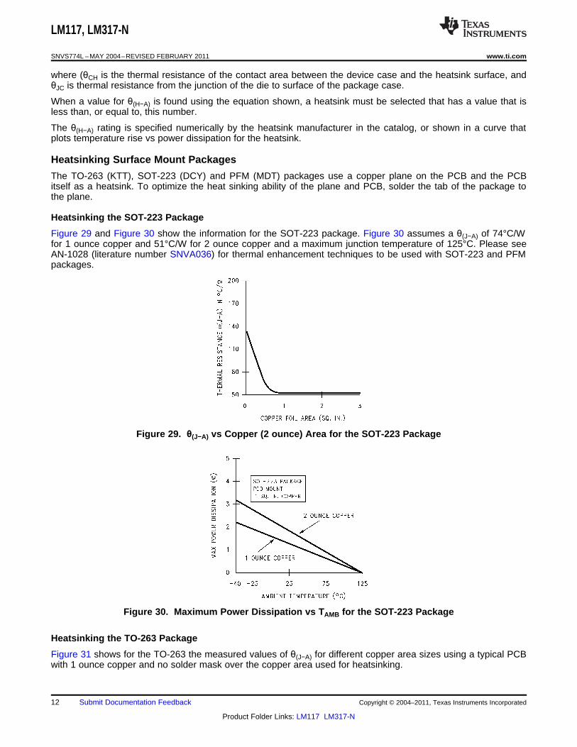
The bypass capacitor on the adjustment terminal can discharge through a low current junction. Discharge occurswhen either the input, or the output, is shorted. Internal to the LM117 is a 50Ω resistor which limits the peakdischarge current. No protection is needed for output voltages of 25V or less and 10 μF capacitance. Figure 27shows an LM117 with protection diodes included for use with outputs greater than 25V and high values of outputcapacitance.
10 Submit Documentation Feedback Copyright © 2004–2011, Texas Instruments Incorporated
Product Folder Links: LM117 LM317-N
LM117, LM317-N
www.ti.com SNVS774L –MAY 2004–REVISED FEBRUARY 2011
D1 protects against C1D2 protects against C2
Figure 27. Regulator with Protection Diodes
Heatsink Requirements
The LM317-N regulators have internal thermal shutdown to protect the device from over-heating. Under alloperating conditions, the junction temperature of the LM317-N should not exceed the rated maximum junctiontemperature (TJ) of 150°C for the LM117, or 125°C for the LM317A and LM317-N. A heatsink may be requireddepending on the maximum device power dissipation and the maximum ambient temperature of the application.To determine if a heatsink is needed, the power dissipated by the regulator, PD, must be calculated:
PD = ((VIN − VOUT) × IL) + (VIN × IG) (2)
Figure 28 shows the voltage and currents which are present in the circuit.
The next parameter which must be calculated is the maximum allowable temperature rise, TR(MAX):TR(MAX) = TJ(MAX) − TA(MAX) (3)
where TJ(MAX) is the maximum allowable junction temperature (150°C for the LM117, or 125°C for theLM317A/LM317-N), and TA(MAX) is the maximum ambient temperature which will be encountered in theapplication.
Using the calculated values for TR(MAX) and PD, the maximum allowable value for the junction-to-ambient thermalresistance (θJA) can be calculated:
θJA = (TR(MAX) / PD) (4)
Figure 28. Power Dissipation Diagram
If the calculated maximum allowable thermal resistance is higher than the actual package rating, then noadditional work is needed. If the calculated maximum allowable thermal resistance is lower than the actualpackage rating either the power dissipation (PD) needs to be reduced, the maximum ambient temperature TA(MAX)needs to be reduced, the thermal resistance (θJA) must be lowered by adding a heatsink, or some combination ofthese.
If a heatsink is needed, the value can be calculated from the formula:θHA ≤ (θJA - (θCH + θJC)) (5)
Copyright © 2004–2011, Texas Instruments Incorporated Submit Documentation Feedback 11
Product Folder Links: LM117 LM317-N
LM117, LM317-N
SNVS774L –MAY 2004–REVISED FEBRUARY 2011 www.ti.com
where (θCH is the thermal resistance of the contact area between the device case and the heatsink surface, andθJC is thermal resistance from the junction of the die to surface of the package case.
When a value for θ(H−A) is found using the equation shown, a heatsink must be selected that has a value that isless than, or equal to, this number.
The θ(H−A) rating is specified numerically by the heatsink manufacturer in the catalog, or shown in a curve thatplots temperature rise vs power dissipation for the heatsink.
Heatsinking Surface Mount Packages
The TO-263 (KTT), SOT-223 (DCY) and PFM (MDT) packages use a copper plane on the PCB and the PCBitself as a heatsink. To optimize the heat sinking ability of the plane and PCB, solder the tab of the package tothe plane.
Heatsinking the SOT-223 Package
Figure 29 and Figure 30 show the information for the SOT-223 package. Figure 30 assumes a θ(J−A) of 74°C/Wfor 1 ounce copper and 51°C/W for 2 ounce copper and a maximum junction temperature of 125°C. Please seeAN-1028 (literature number SNVA036) for thermal enhancement techniques to be used with SOT-223 and PFMpackages.
Figure 29. θ(J−A) vs Copper (2 ounce) Area for the SOT-223 Package
Figure 30. Maximum Power Dissipation vs TAMB for the SOT-223 Package
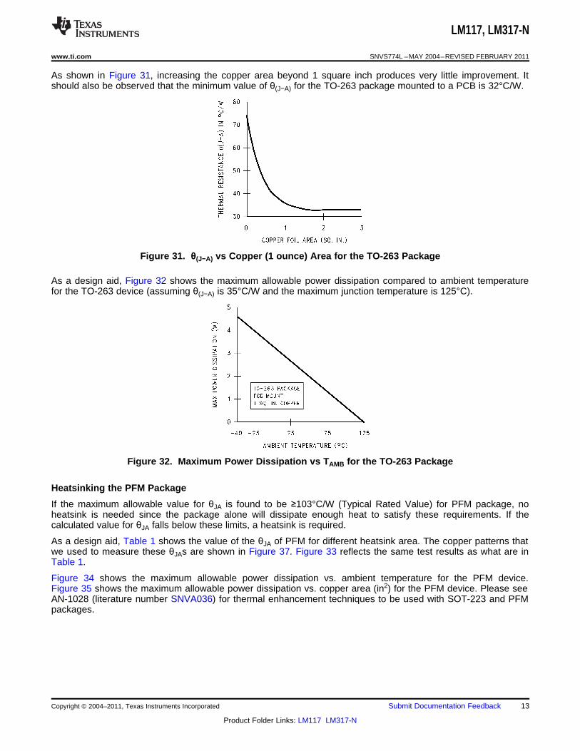
Heatsinking the TO-263 Package
Figure 31 shows for the TO-263 the measured values of θ(J−A) for different copper area sizes using a typical PCBwith 1 ounce copper and no solder mask over the copper area used for heatsinking.
12 Submit Documentation Feedback Copyright © 2004–2011, Texas Instruments Incorporated
Product Folder Links: LM117 LM317-N
LM117, LM317-N
www.ti.com SNVS774L –MAY 2004–REVISED FEBRUARY 2011
As shown in Figure 31, increasing the copper area beyond 1 square inch produces very little improvement. Itshould also be observed that the minimum value of θ(J−A) for the TO-263 package mounted to a PCB is 32°C/W.
Figure 31. θ(J−A) vs Copper (1 ounce) Area for the TO-263 Package
As a design aid, Figure 32 shows the maximum allowable power dissipation compared to ambient temperaturefor the TO-263 device (assuming θ(J−A) is 35°C/W and the maximum junction temperature is 125°C).
Figure 32. Maximum Power Dissipation vs TAMB for the TO-263 Package
Heatsinking the PFM Package
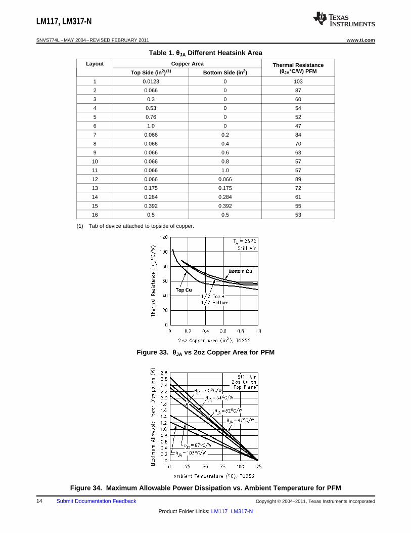
If the maximum allowable value for θJA is found to be ≥103°C/W (Typical Rated Value) for PFM package, noheatsink is needed since the package alone will dissipate enough heat to satisfy these requirements. If thecalculated value for θJA falls below these limits, a heatsink is required.
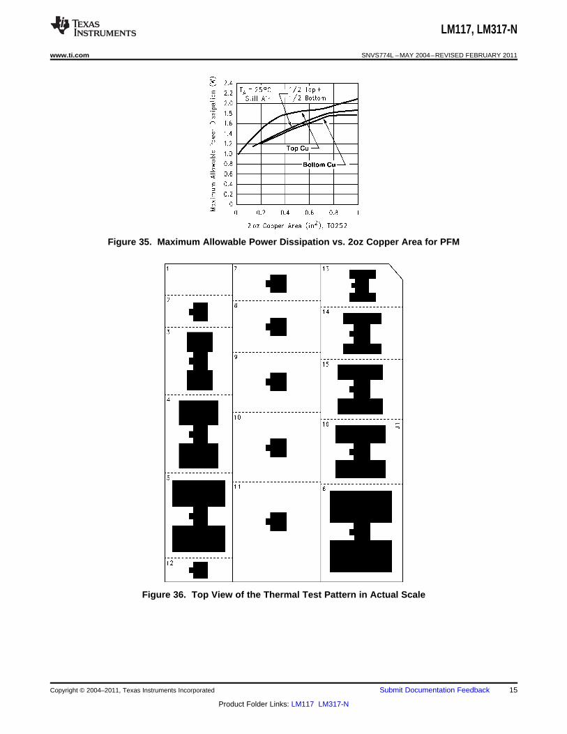
As a design aid, Table 1 shows the value of the θJA of PFM for different heatsink area. The copper patterns thatwe used to measure these θJAs are shown in Figure 37. Figure 33 reflects the same test results as what are inTable 1.
Figure 34 shows the maximum allowable power dissipation vs. ambient temperature for the PFM device.Figure 35 shows the maximum allowable power dissipation vs. copper area (in2) for the PFM device. Please seeAN-1028 (literature number SNVA036) for thermal enhancement techniques to be used with SOT-223 and PFMpackages.
Copyright © 2004–2011, Texas Instruments Incorporated Submit Documentation Feedback 13
Product Folder Links: LM117 LM317-N
LM117, LM317-N
SNVS774L –MAY 2004–REVISED FEBRUARY 2011 www.ti.com
Table 1. θJA Different Heatsink Area
Layout Copper Area Thermal Resistance(θJA°C/W) PFMTop Side (in2) (1) Bottom Side (in2)
1 0.0123 0 103
2 0.066 0 87
3 0.3 0 60
4 0.53 0 54
5 0.76 0 52
6 1.0 0 47
7 0.066 0.2 84
8 0.066 0.4 70
9 0.066 0.6 63
10 0.066 0.8 57
11 0.066 1.0 57
12 0.066 0.066 89
13 0.175 0.175 72
14 0.284 0.284 61
15 0.392 0.392 55
16 0.5 0.5 53
(1) Tab of device attached to topside of copper.
Figure 33. θJA vs 2oz Copper Area for PFM
Figure 34. Maximum Allowable Power Dissipation vs. Ambient Temperature for PFM
14 Submit Documentation Feedback Copyright © 2004–2011, Texas Instruments Incorporated
Product Folder Links: LM117 LM317-N
LM117, LM317-N
www.ti.com SNVS774L –MAY 2004–REVISED FEBRUARY 2011
Figure 35. Maximum Allowable Power Dissipation vs. 2oz Copper Area for PFM
Figure 36. Top View of the Thermal Test Pattern in Actual Scale
Copyright © 2004–2011, Texas Instruments Incorporated Submit Documentation Feedback 15
Product Folder Links: LM117 LM317-N
LM117, LM317-N
SNVS774L –MAY 2004–REVISED FEBRUARY 2011 www.ti.com
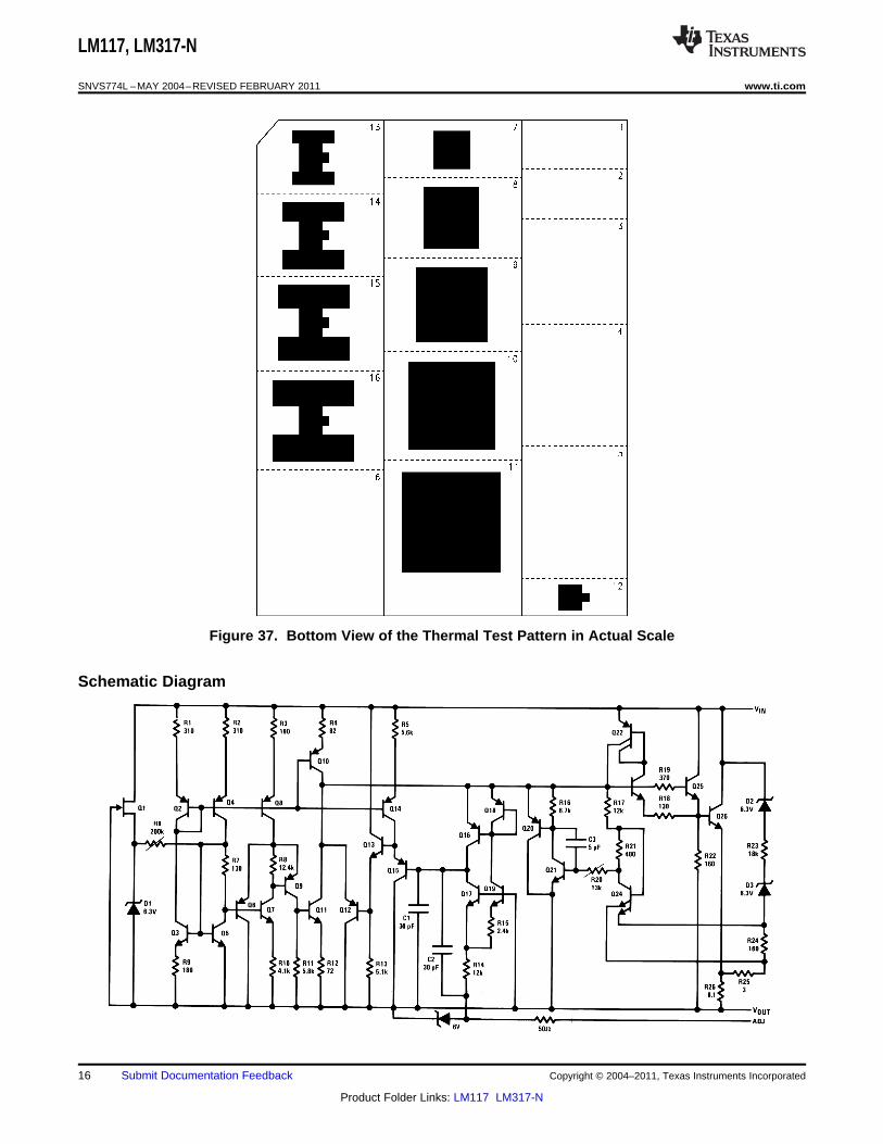
Figure 37. Bottom View of the Thermal Test Pattern in Actual Scale
Schematic Diagram
16 Submit Documentation Feedback Copyright © 2004–2011, Texas Instruments Incorporated
Product Folder Links: LM117 LM317-N
LM117, LM317-N
www.ti.com SNVS774L –MAY 2004–REVISED FEBRUARY 2011
Typical Applications
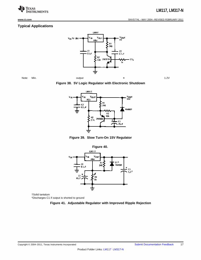
Note: Min. output ≊ 1.2V
Figure 38. 5V Logic Regulator with Electronic Shutdown
Figure 39. Slow Turn-On 15V Regulator
Figure 40.
†Solid tantalum*Discharges C1 if output is shorted to ground
Figure 41. Adjustable Regulator with Improved Ripple Rejection
Copyright © 2004–2011, Texas Instruments Incorporated Submit Documentation Feedback 17
Product Folder Links: LM117 LM317-N
LM117, LM317-N
SNVS774L –MAY 2004–REVISED FEBRUARY 2011 www.ti.com
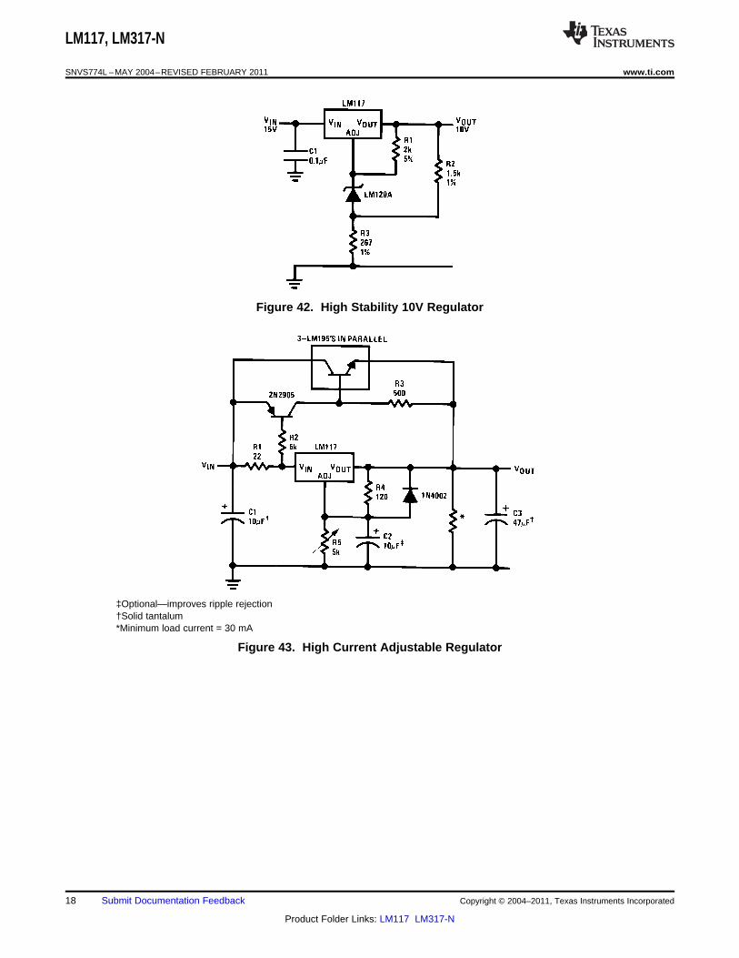
Figure 42. High Stability 10V Regulator
‡Optional—improves ripple rejection†Solid tantalum*Minimum load current = 30 mA
Figure 43. High Current Adjustable Regulator
18 Submit Documentation Feedback Copyright © 2004–2011, Texas Instruments Incorporated
Product Folder Links: LM117 LM317-N
LM117, LM317-N
www.ti.com SNVS774L –MAY 2004–REVISED FEBRUARY 2011
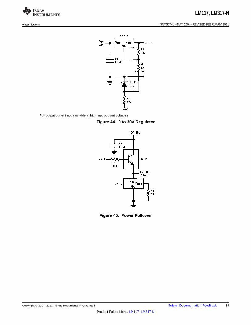
Full output current not available at high input-output voltages
Figure 44. 0 to 30V Regulator
Figure 45. Power Follower
Copyright © 2004–2011, Texas Instruments Incorporated Submit Documentation Feedback 19
Product Folder Links: LM117 LM317-N
LM117, LM317-N
SNVS774L –MAY 2004–REVISED FEBRUARY 2011 www.ti.com
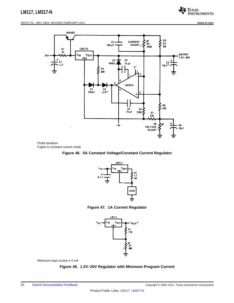
†Solid tantalum*Lights in constant current mode
Figure 46. 5A Constant Voltage/Constant Current Regulator
Figure 47. 1A Current Regulator
*Minimum load current ≊ 4 mA
Figure 48. 1.2V–20V Regulator with Minimum Program Current
20 Submit Documentation Feedback Copyright © 2004–2011, Texas Instruments Incorporated
Product Folder Links: LM117 LM317-N
LM117, LM317-N
www.ti.com SNVS774L –MAY 2004–REVISED FEBRUARY 2011
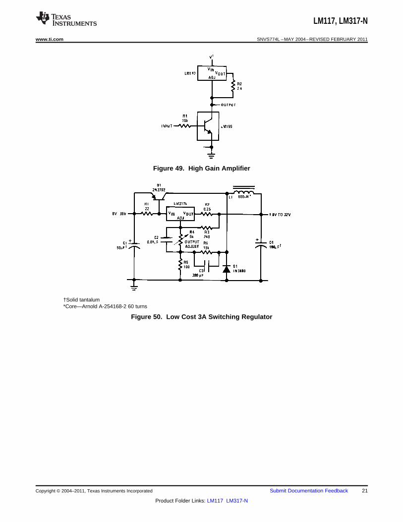
Figure 49. High Gain Amplifier
†Solid tantalum*Core—Arnold A-254168-2 60 turns
Figure 50. Low Cost 3A Switching Regulator
Copyright © 2004–2011, Texas Instruments Incorporated Submit Documentation Feedback 21
Product Folder Links: LM117 LM317-N
LM117, LM317-N
SNVS774L –MAY 2004–REVISED FEBRUARY 2011 www.ti.com
†Solid tantalum*Core—Arnold A-254168-2 60 turns
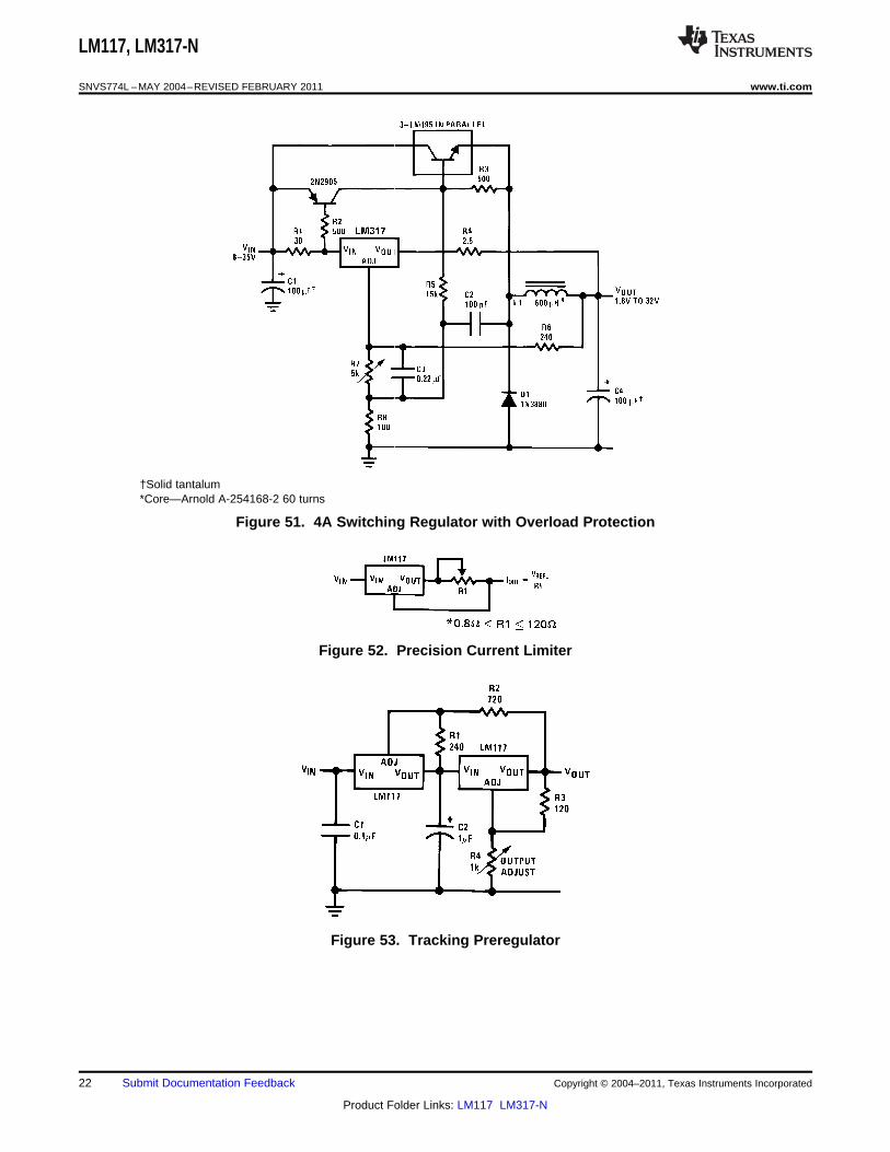
Figure 51. 4A Switching Regulator with Overload Protection
Figure 52. Precision Current Limiter
Figure 53. Tracking Preregulator
22 Submit Documentation Feedback Copyright © 2004–2011, Texas Instruments Incorporated
Product Folder Links: LM117 LM317-N
LM117, LM317-N
www.ti.com SNVS774L –MAY 2004–REVISED FEBRUARY 2011
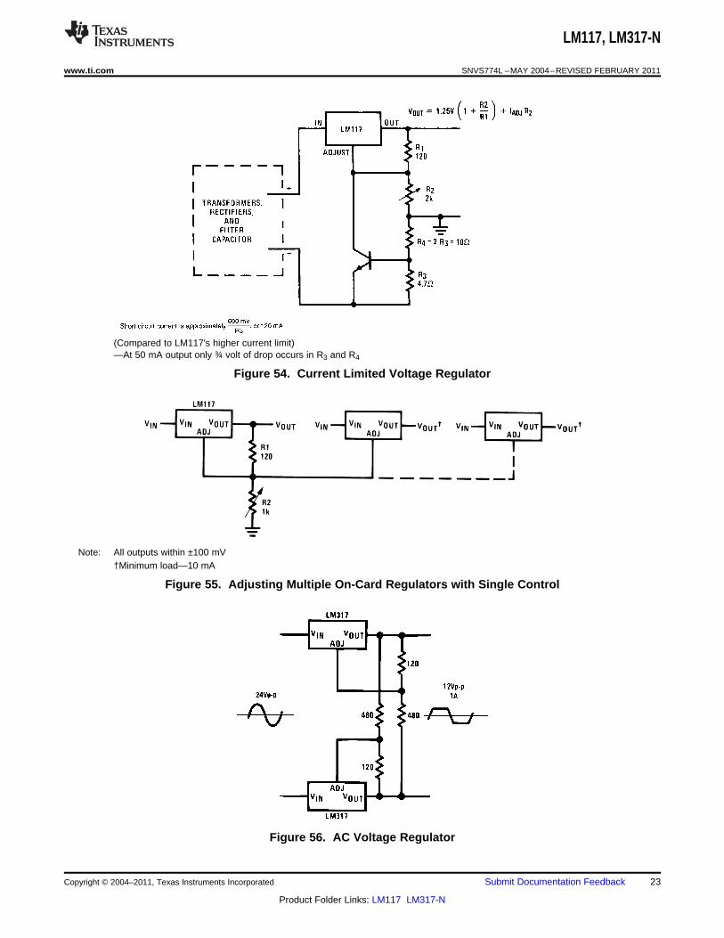
(Compared to LM117's higher current limit)—At 50 mA output only ¾ volt of drop occurs in R3 and R4
Figure 54. Current Limited Voltage Regulator
Note: All outputs within ±100 mV†Minimum load—10 mA
Figure 55. Adjusting Multiple On-Card Regulators with Single Control
Figure 56. AC Voltage Regulator
Copyright © 2004–2011, Texas Instruments Incorporated Submit Documentation Feedback 23
Product Folder Links: LM117 LM317-N
LM117, LM317-N
SNVS774L –MAY 2004–REVISED FEBRUARY 2011 www.ti.com
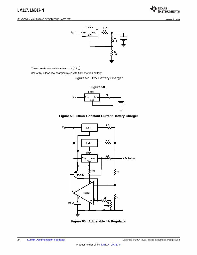
Use of RS allows low charging rates with fully charged battery.
Figure 57. 12V Battery Charger
Figure 58.
Figure 59. 50mA Constant Current Battery Charger
Figure 60. Adjustable 4A Regulator
24 Submit Documentation Feedback Copyright © 2004–2011, Texas Instruments Incorporated
Product Folder Links: LM117 LM317-N
LM117, LM317-N
www.ti.com SNVS774L –MAY 2004–REVISED FEBRUARY 2011
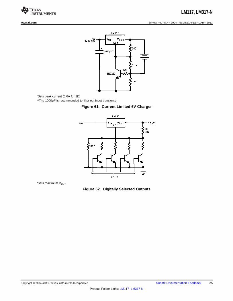
*Sets peak current (0.6A for 1Ω)**The 1000μF is recommended to filter out input transients
Figure 61. Current Limited 6V Charger
*Sets maximum VOUT
Figure 62. Digitally Selected Outputs
Copyright © 2004–2011, Texas Instruments Incorporated Submit Documentation Feedback 25
Product Folder Links: LM117 LM317-N
PACKAGE OPTION ADDENDUM
www.ti.com 29-May-2013
Addendum-Page 1
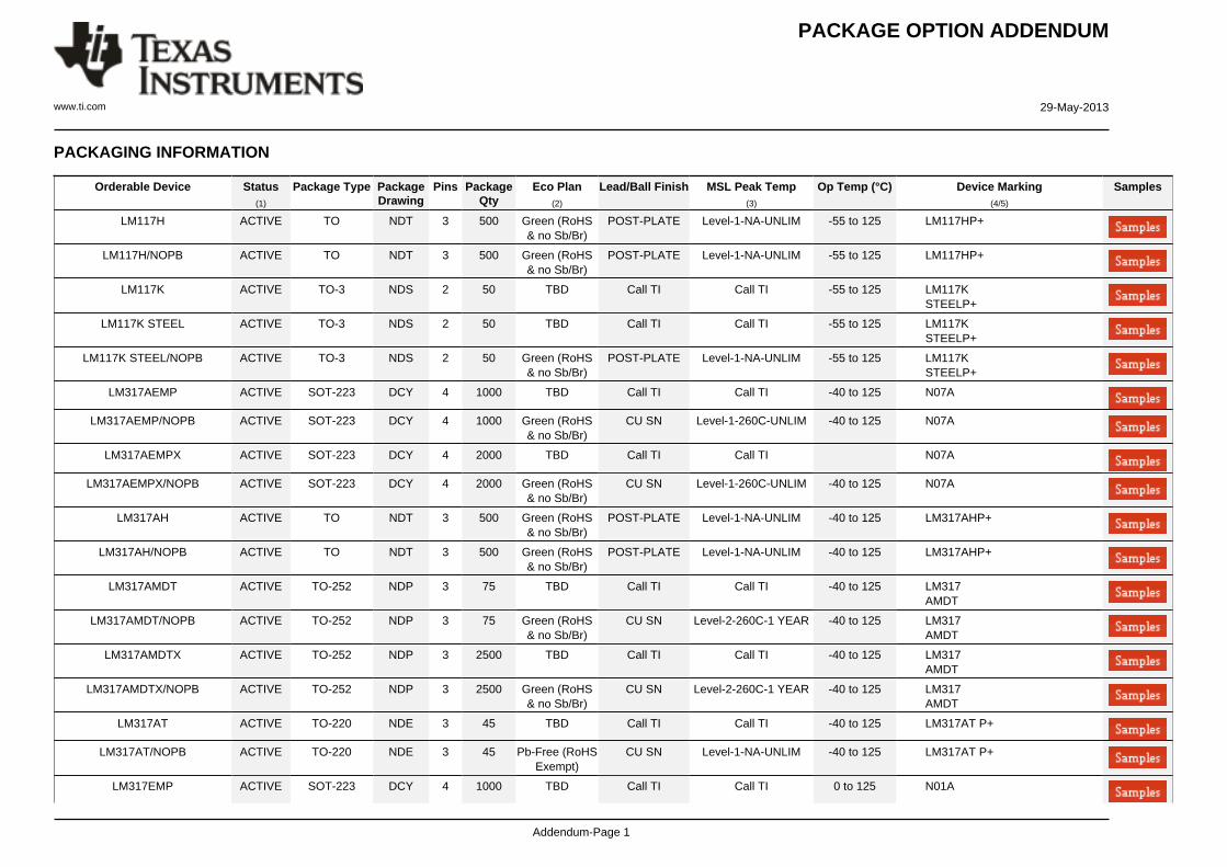
PACKAGING INFORMATION
Orderable Device Status(1)
Package Type PackageDrawing
Pins PackageQty
Eco Plan(2)
Lead/Ball Finish MSL Peak Temp(3)
Op Temp (°C) Device Marking(4/5)
Samples
LM117H ACTIVE TO NDT 3 500 Green (RoHS& no Sb/Br)
POST-PLATE Level-1-NA-UNLIM -55 to 125 LM117HP+
LM117H/NOPB ACTIVE TO NDT 3 500 Green (RoHS& no Sb/Br)
POST-PLATE Level-1-NA-UNLIM -55 to 125 LM117HP+
LM117K ACTIVE TO-3 NDS 2 50 TBD Call TI Call TI -55 to 125 LM117KSTEELP+
LM117K STEEL ACTIVE TO-3 NDS 2 50 TBD Call TI Call TI -55 to 125 LM117KSTEELP+
LM117K STEEL/NOPB ACTIVE TO-3 NDS 2 50 Green (RoHS& no Sb/Br)
POST-PLATE Level-1-NA-UNLIM -55 to 125 LM117KSTEELP+
LM317AEMP ACTIVE SOT-223 DCY 4 1000 TBD Call TI Call TI -40 to 125 N07A
LM317AEMP/NOPB ACTIVE SOT-223 DCY 4 1000 Green (RoHS& no Sb/Br)
CU SN Level-1-260C-UNLIM -40 to 125 N07A
LM317AEMPX ACTIVE SOT-223 DCY 4 2000 TBD Call TI Call TI N07A
LM317AEMPX/NOPB ACTIVE SOT-223 DCY 4 2000 Green (RoHS& no Sb/Br)
CU SN Level-1-260C-UNLIM -40 to 125 N07A
LM317AH ACTIVE TO NDT 3 500 Green (RoHS& no Sb/Br)
POST-PLATE Level-1-NA-UNLIM -40 to 125 LM317AHP+
LM317AH/NOPB ACTIVE TO NDT 3 500 Green (RoHS& no Sb/Br)
POST-PLATE Level-1-NA-UNLIM -40 to 125 LM317AHP+
LM317AMDT ACTIVE TO-252 NDP 3 75 TBD Call TI Call TI -40 to 125 LM317AMDT
LM317AMDT/NOPB ACTIVE TO-252 NDP 3 75 Green (RoHS& no Sb/Br)
CU SN Level-2-260C-1 YEAR -40 to 125 LM317AMDT
LM317AMDTX ACTIVE TO-252 NDP 3 2500 TBD Call TI Call TI -40 to 125 LM317AMDT
LM317AMDTX/NOPB ACTIVE TO-252 NDP 3 2500 Green (RoHS& no Sb/Br)
CU SN Level-2-260C-1 YEAR -40 to 125 LM317AMDT
LM317AT ACTIVE TO-220 NDE 3 45 TBD Call TI Call TI -40 to 125 LM317AT P+
LM317AT/NOPB ACTIVE TO-220 NDE 3 45 Pb-Free (RoHSExempt)
CU SN Level-1-NA-UNLIM -40 to 125 LM317AT P+
LM317EMP ACTIVE SOT-223 DCY 4 1000 TBD Call TI Call TI 0 to 125 N01A
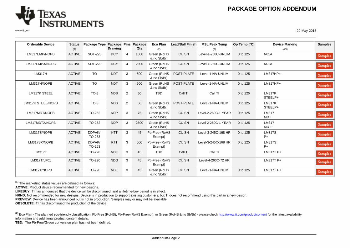
PACKAGE OPTION ADDENDUM
www.ti.com 29-May-2013
Addendum-Page 2
Orderable Device Status(1)
Package Type PackageDrawing
Pins PackageQty
Eco Plan(2)
Lead/Ball Finish MSL Peak Temp(3)
Op Temp (°C) Device Marking(4/5)
Samples
LM317EMP/NOPB ACTIVE SOT-223 DCY 4 1000 Green (RoHS& no Sb/Br)
CU SN Level-1-260C-UNLIM 0 to 125 N01A
LM317EMPX/NOPB ACTIVE SOT-223 DCY 4 2000 Green (RoHS& no Sb/Br)
CU SN Level-1-260C-UNLIM 0 to 125 N01A
LM317H ACTIVE TO NDT 3 500 Green (RoHS& no Sb/Br)
POST-PLATE Level-1-NA-UNLIM 0 to 125 LM317HP+
LM317H/NOPB ACTIVE TO NDT 3 500 Green (RoHS& no Sb/Br)
POST-PLATE Level-1-NA-UNLIM 0 to 125 LM317HP+
LM317K STEEL ACTIVE TO-3 NDS 2 50 TBD Call TI Call TI 0 to 125 LM317KSTEELP+
LM317K STEEL/NOPB ACTIVE TO-3 NDS 2 50 Green (RoHS& no Sb/Br)
POST-PLATE Level-1-NA-UNLIM 0 to 125 LM317KSTEELP+
LM317MDT/NOPB ACTIVE TO-252 NDP 3 75 Green (RoHS& no Sb/Br)
CU SN Level-2-260C-1 YEAR 0 to 125 LM317MDT
LM317MDTX/NOPB ACTIVE TO-252 NDP 3 2500 Green (RoHS& no Sb/Br)
CU SN Level-2-260C-1 YEAR 0 to 125 LM317MDT
LM317S/NOPB ACTIVE DDPAK/TO-263
KTT 3 45 Pb-Free (RoHSExempt)
CU SN Level-3-245C-168 HR 0 to 125 LM317SP+
LM317SX/NOPB ACTIVE DDPAK/TO-263
KTT 3 500 Pb-Free (RoHSExempt)
CU SN Level-3-245C-168 HR 0 to 125 LM317SP+
LM317T ACTIVE TO-220 NDE 3 45 TBD Call TI Call TI LM317T P+
LM317T/LF01 ACTIVE TO-220 NDG 3 45 Pb-Free (RoHSExempt)
CU SN Level-4-260C-72 HR LM317T P+
LM317T/NOPB ACTIVE TO-220 NDE 3 45 Green (RoHS& no Sb/Br)
CU SN Level-1-NA-UNLIM 0 to 125 LM317T P+
(1) The marketing status values are defined as follows:ACTIVE: Product device recommended for new designs.LIFEBUY: TI has announced that the device will be discontinued, and a lifetime-buy period is in effect.NRND: Not recommended for new designs. Device is in production to support existing customers, but TI does not recommend using this part in a new design.PREVIEW: Device has been announced but is not in production. Samples may or may not be available.OBSOLETE: TI has discontinued the production of the device.
(2) Eco Plan - The planned eco-friendly classification: Pb-Free (RoHS), Pb-Free (RoHS Exempt), or Green (RoHS & no Sb/Br) - please check http://www.ti.com/productcontent for the latest availabilityinformation and additional product content details.TBD: The Pb-Free/Green conversion plan has not been defined.
PACKAGE OPTION ADDENDUM
www.ti.com 29-May-2013
Addendum-Page 3
Pb-Free (RoHS): TI's terms "Lead-Free" or "Pb-Free" mean semiconductor products that are compatible with the current RoHS requirements for all 6 substances, including the requirement thatlead not exceed 0.1% by weight in homogeneous materials. Where designed to be soldered at high temperatures, TI Pb-Free products are suitable for use in specified lead-free processes.Pb-Free (RoHS Exempt): This component has a RoHS exemption for either 1) lead-based flip-chip solder bumps used between the die and package, or 2) lead-based die adhesive used betweenthe die and leadframe. The component is otherwise considered Pb-Free (RoHS compatible) as defined above.Green (RoHS & no Sb/Br): TI defines "Green" to mean Pb-Free (RoHS compatible), and free of Bromine (Br) and Antimony (Sb) based flame retardants (Br or Sb do not exceed 0.1% by weightin homogeneous material)
(3) MSL, Peak Temp. -- The Moisture Sensitivity Level rating according to the JEDEC industry standard classifications, and peak solder temperature.
(4) There may be additional marking, which relates to the logo, the lot trace code information, or the environmental category on the device.
(5) Multiple Device Markings will be inside parentheses. Only one Device Marking contained in parentheses and separated by a "~" will appear on a device. If a line is indented then it is a continuationof the previous line and the two combined represent the entire Device Marking for that device.
Important Information and Disclaimer:The information provided on this page represents TI's knowledge and belief as of the date that it is provided. TI bases its knowledge and belief on informationprovided by third parties, and makes no representation or warranty as to the accuracy of such information. Efforts are underway to better integrate information from third parties. TI has taken andcontinues to take reasonable steps to provide representative and accurate information but may not have conducted destructive testing or chemical analysis on incoming materials and chemicals.TI and TI suppliers consider certain information to be proprietary, and thus CAS numbers and other limited information may not be available for release.
In no event shall TI's liability arising out of such information exceed the total purchase price of the TI part(s) at issue in this document sold by TI to Customer on an annual basis.
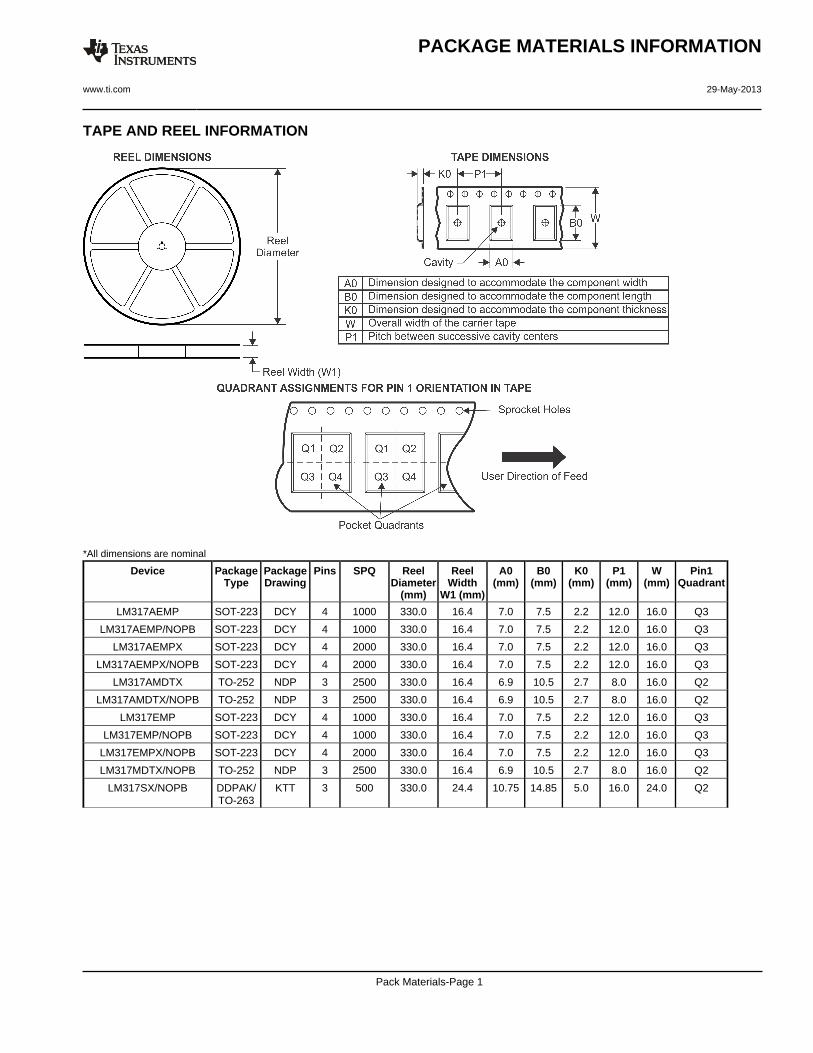
TAPE AND REEL INFORMATION
*All dimensions are nominal
Device PackageType
PackageDrawing
Pins SPQ ReelDiameter
(mm)
ReelWidth
W1 (mm)
A0(mm)
B0(mm)
K0(mm)
P1(mm)
W(mm)
Pin1Quadrant
LM317AEMP SOT-223 DCY 4 1000 330.0 16.4 7.0 7.5 2.2 12.0 16.0 Q3
LM317AEMP/NOPB SOT-223 DCY 4 1000 330.0 16.4 7.0 7.5 2.2 12.0 16.0 Q3
LM317AEMPX SOT-223 DCY 4 2000 330.0 16.4 7.0 7.5 2.2 12.0 16.0 Q3
LM317AEMPX/NOPB SOT-223 DCY 4 2000 330.0 16.4 7.0 7.5 2.2 12.0 16.0 Q3
LM317AMDTX TO-252 NDP 3 2500 330.0 16.4 6.9 10.5 2.7 8.0 16.0 Q2
LM317AMDTX/NOPB TO-252 NDP 3 2500 330.0 16.4 6.9 10.5 2.7 8.0 16.0 Q2
LM317EMP SOT-223 DCY 4 1000 330.0 16.4 7.0 7.5 2.2 12.0 16.0 Q3
LM317EMP/NOPB SOT-223 DCY 4 1000 330.0 16.4 7.0 7.5 2.2 12.0 16.0 Q3
LM317EMPX/NOPB SOT-223 DCY 4 2000 330.0 16.4 7.0 7.5 2.2 12.0 16.0 Q3
LM317MDTX/NOPB TO-252 NDP 3 2500 330.0 16.4 6.9 10.5 2.7 8.0 16.0 Q2
LM317SX/NOPB DDPAK/TO-263
KTT 3 500 330.0 24.4 10.75 14.85 5.0 16.0 24.0 Q2
PACKAGE MATERIALS INFORMATION
www.ti.com 29-May-2013
Pack Materials-Page 1
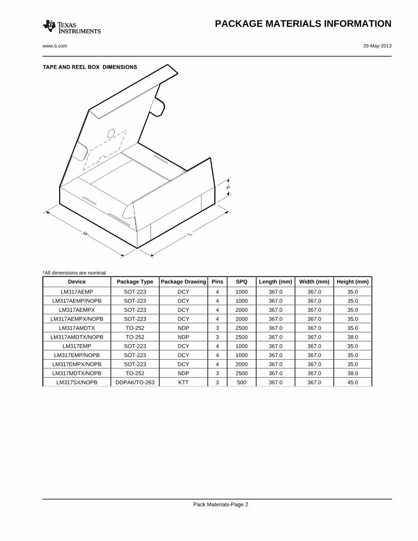
*All dimensions are nominal
Device Package Type Package Drawing Pins SPQ Length (mm) Width (mm) Height (mm)
LM317AEMP SOT-223 DCY 4 1000 367.0 367.0 35.0
LM317AEMP/NOPB SOT-223 DCY 4 1000 367.0 367.0 35.0
LM317AEMPX SOT-223 DCY 4 2000 367.0 367.0 35.0
LM317AEMPX/NOPB SOT-223 DCY 4 2000 367.0 367.0 35.0
LM317AMDTX TO-252 NDP 3 2500 367.0 367.0 35.0
LM317AMDTX/NOPB TO-252 NDP 3 2500 367.0 367.0 38.0
LM317EMP SOT-223 DCY 4 1000 367.0 367.0 35.0
LM317EMP/NOPB SOT-223 DCY 4 1000 367.0 367.0 35.0
LM317EMPX/NOPB SOT-223 DCY 4 2000 367.0 367.0 35.0
LM317MDTX/NOPB TO-252 NDP 3 2500 367.0 367.0 38.0
LM317SX/NOPB DDPAK/TO-263 KTT 3 500 367.0 367.0 45.0
PACKAGE MATERIALS INFORMATION
www.ti.com 29-May-2013
Pack Materials-Page 2
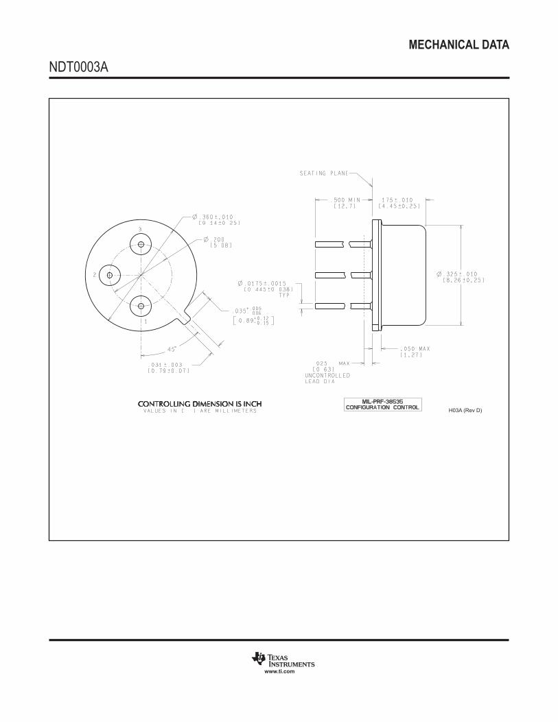
MECHANICAL DATA
NDT0003A
www.ti.com
H03A (Rev D)
MECHANICAL DATA
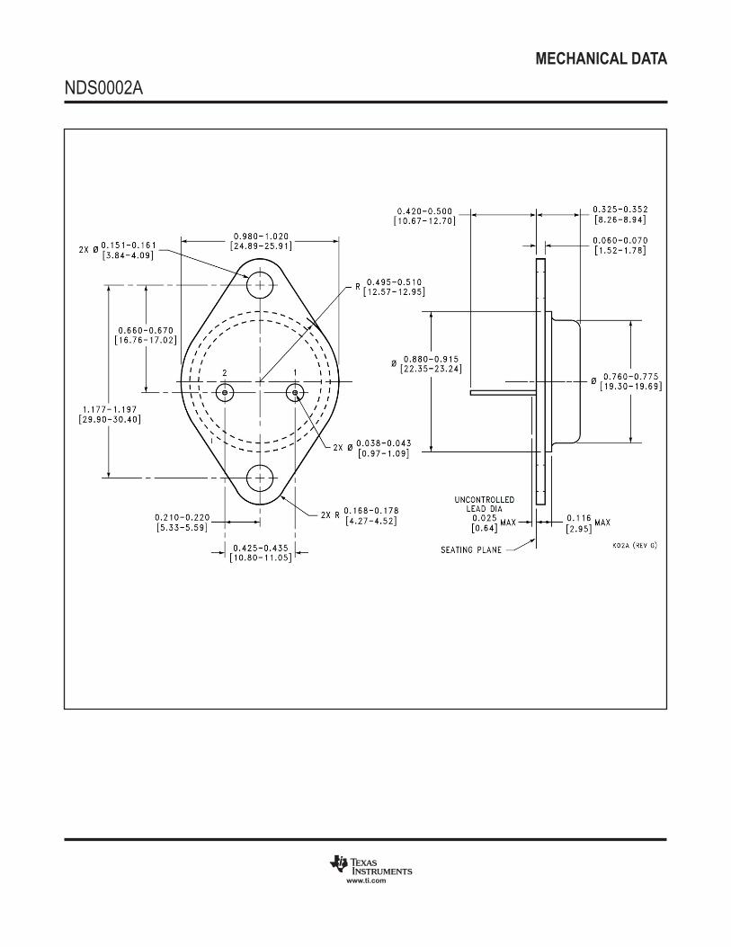
NDS0002A
www.ti.com
MECHANICAL DATA
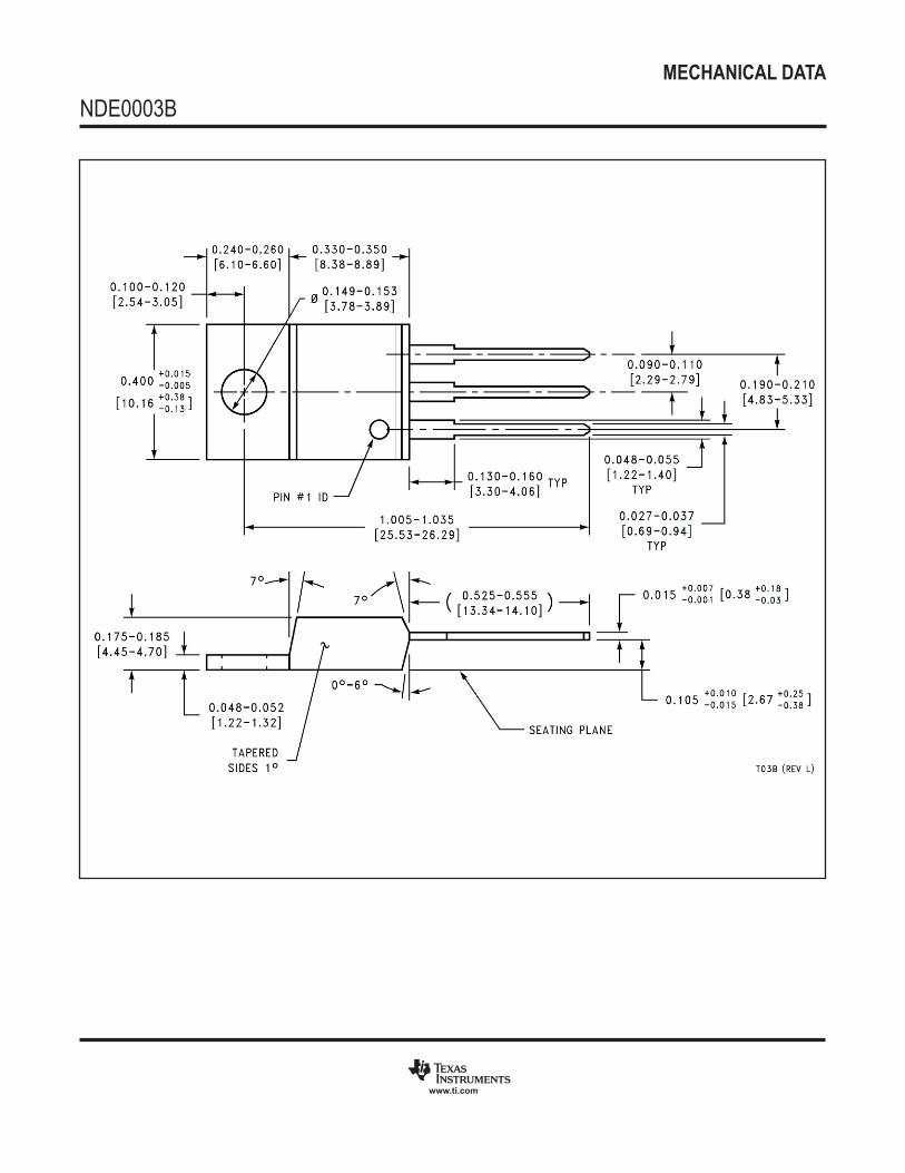
NDE0003B
www.ti.com
MECHANICAL DATA
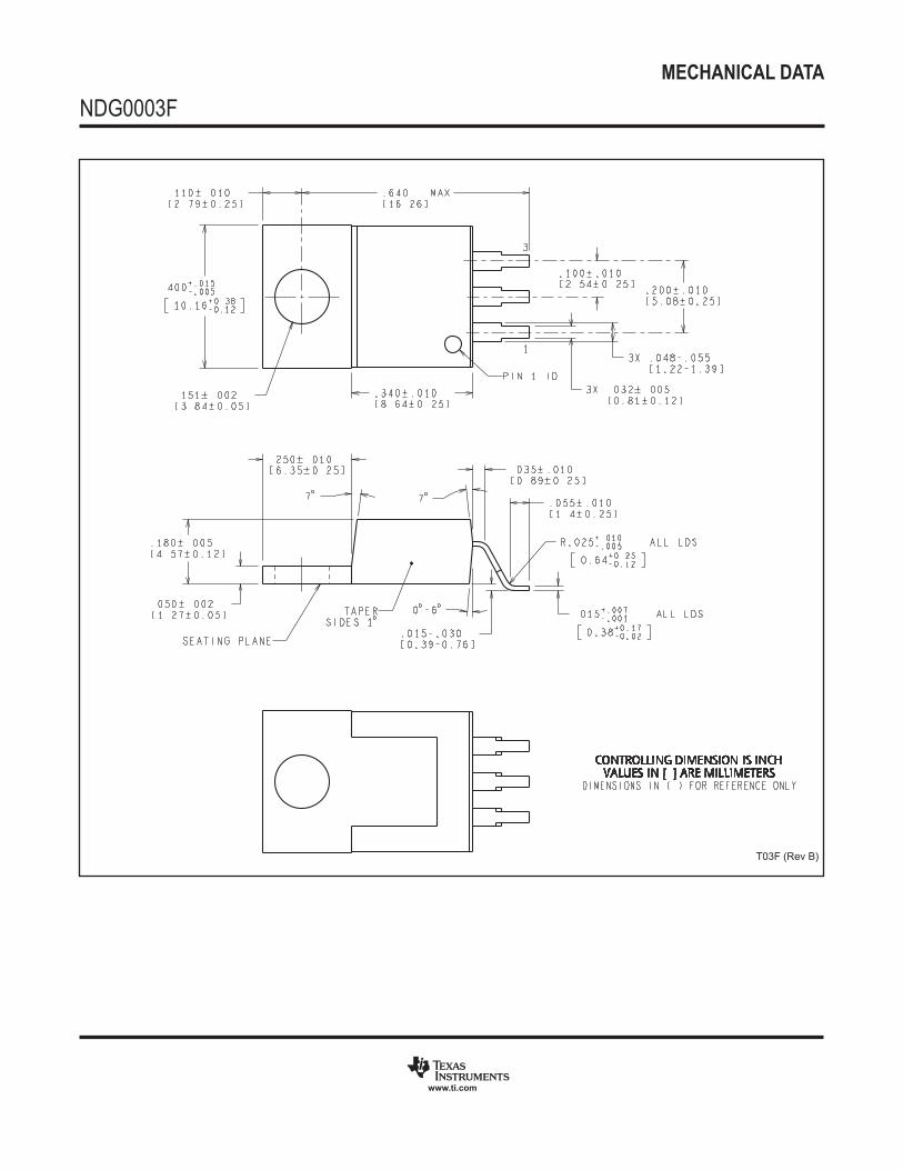
NDG0003F
www.ti.com
T03F (Rev B)
MECHANICAL DATA
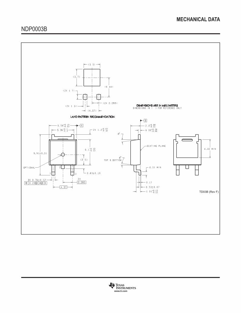
NDP0003B
www.ti.com
TD03B (Rev F)
MECHANICAL DATA
MPDS094A – APRIL 2001 – REVISED JUNE 2002
POST OFFICE BOX 655303 • DALLAS, TEXAS 75265
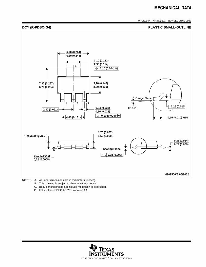
DCY (R-PDSO-G4) PLASTIC SMALL-OUTLINE
4202506/B 06/2002
6,30 (0.248)6,70 (0.264)
2,90 (0.114)3,10 (0.122)
6,70 (0.264)7,30 (0.287) 3,70 (0.146)
3,30 (0.130)
0,02 (0.0008)0,10 (0.0040)
1,50 (0.059)1,70 (0.067)
0,23 (0.009)0,35 (0.014)
1 2 3
4
0,66 (0.026)0,84 (0.033)
1,80 (0.071) MAX
Seating Plane
0°–10°
Gauge Plane
0,75 (0.030) MIN
0,25 (0.010)
0,08 (0.003)
0,10 (0.004) M
2,30 (0.091)
4,60 (0.181) M0,10 (0.004)
NOTES: A. All linear dimensions are in millimeters (inches).B. This drawing is subject to change without notice.C. Body dimensions do not include mold flash or protrusion.D. Falls within JEDEC TO-261 Variation AA.
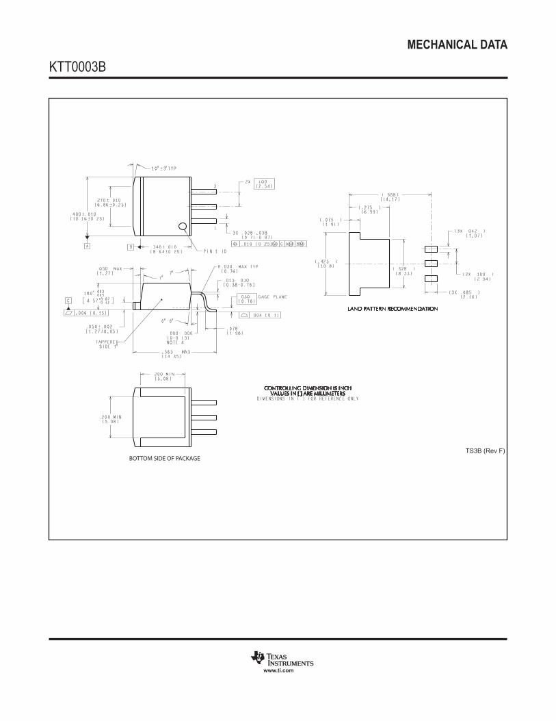
MECHANICAL DATA
KTT0003B
www.ti.com
BOTTOM SIDE OF PACKAGETS3B (Rev F)
IMPORTANT NOTICE
Texas Instruments Incorporated and its subsidiaries (TI) reserve the right to make corrections, enhancements, improvements and otherchanges to its semiconductor products and services per JESD46, latest issue, and to discontinue any product or service per JESD48, latestissue. Buyers should obtain the latest relevant information before placing orders and should verify that such information is current andcomplete. All semiconductor products (also referred to herein as “components”) are sold subject to TI’s terms and conditions of salesupplied at the time of order acknowledgment.
TI warrants performance of its components to the specifications applicable at the time of sale, in accordance with the warranty in TI’s termsand conditions of sale of semiconductor products. Testing and other quality control techniques are used to the extent TI deems necessaryto support this warranty. Except where mandated by applicable law, testing of all parameters of each component is not necessarilyperformed.
TI assumes no liability for applications assistance or the design of Buyers’ products. Buyers are responsible for their products andapplications using TI components. To minimize the risks associated with Buyers’ products and applications, Buyers should provideadequate design and operating safeguards.
TI does not warrant or represent that any license, either express or implied, is granted under any patent right, copyright, mask work right, orother intellectual property right relating to any combination, machine, or process in which TI components or services are used. Informationpublished by TI regarding third-party products or services does not constitute a license to use such products or services or a warranty orendorsement thereof. Use of such information may require a license from a third party under the patents or other intellectual property of thethird party, or a license from TI under the patents or other intellectual property of TI.
Reproduction of significant portions of TI information in TI data books or data sheets is permissible only if reproduction is without alterationand is accompanied by all associated warranties, conditions, limitations, and notices. TI is not responsible or liable for such altereddocumentation. Information of third parties may be subject to additional restrictions.
Resale of TI components or services with statements different from or beyond the parameters stated by TI for that component or servicevoids all express and any implied warranties for the associated TI component or service and is an unfair and deceptive business practice.TI is not responsible or liable for any such statements.
Buyer acknowledges and agrees that it is solely responsible for compliance with all legal, regulatory and safety-related requirementsconcerning its products, and any use of TI components in its applications, notwithstanding any applications-related information or supportthat may be provided by TI. Buyer represents and agrees that it has all the necessary expertise to create and implement safeguards whichanticipate dangerous consequences of failures, monitor failures and their consequences, lessen the likelihood of failures that might causeharm and take appropriate remedial actions. Buyer will fully indemnify TI and its representatives against any damages arising out of the useof any TI components in safety-critical applications.
In some cases, TI components may be promoted specifically to facilitate safety-related applications. With such components, TI’s goal is tohelp enable customers to design and create their own end-product solutions that meet applicable functional safety standards andrequirements. Nonetheless, such components are subject to these terms.
No TI components are authorized for use in FDA Class III (or similar life-critical medical equipment) unless authorized officers of the partieshave executed a special agreement specifically governing such use.
Only those TI components which TI has specifically designated as military grade or “enhanced plastic” are designed and intended for use inmilitary/aerospace applications or environments. Buyer acknowledges and agrees that any military or aerospace use of TI componentswhich have not been so designated is solely at the Buyer's risk, and that Buyer is solely responsible for compliance with all legal andregulatory requirements in connection with such use.
TI has specifically designated certain components as meeting ISO/TS16949 requirements, mainly for automotive use. In any case of use ofnon-designated products, TI will not be responsible for any failure to meet ISO/TS16949.
Products Applications
Audio www.ti.com/audio Automotive and Transportation www.ti.com/automotive
Amplifiers amplifier.ti.com Communications and Telecom www.ti.com/communications
Data Converters dataconverter.ti.com Computers and Peripherals www.ti.com/computers
DLP® Products www.dlp.com Consumer Electronics www.ti.com/consumer-apps
DSP dsp.ti.com Energy and Lighting www.ti.com/energy
Clocks and Timers www.ti.com/clocks Industrial www.ti.com/industrial
Interface interface.ti.com Medical www.ti.com/medical
Logic logic.ti.com Security www.ti.com/security
Power Mgmt power.ti.com Space, Avionics and Defense www.ti.com/space-avionics-defense
Microcontrollers microcontroller.ti.com Video and Imaging www.ti.com/video
RFID www.ti-rfid.com
OMAP Applications Processors www.ti.com/omap TI E2E Community e2e.ti.com
Wireless Connectivity www.ti.com/wirelessconnectivity
Mailing Address: Texas Instruments, Post Office Box 655303, Dallas, Texas 75265Copyright © 2013, Texas Instruments Incorporated