Embed Size (px)
Citation preview

Software Defined ModemA commercial platform for wireless handsets
Charles F Sturman
VP Marketing
June 22nd ~ 24th Brussels
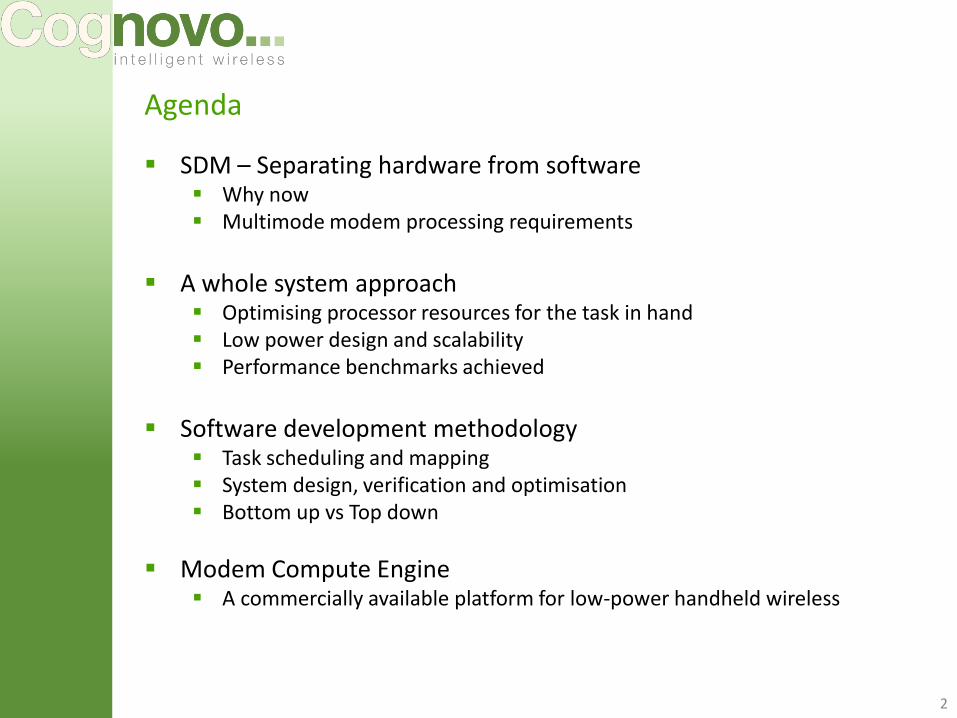
Agenda
SDM – Separating hardware from software Why now Multimode modem processing requirements
A whole system approach Optimising processor resources for the task in hand Low power design and scalability Performance benchmarks achieved
Software development methodology Task scheduling and mapping System design, verification and optimisation Bottom up vs Top down
Modem Compute Engine A commercially available platform for low-power handheld wireless
2

Why Now ?
3
0
50
100
150
200
250
300
350
400
450
500
1990 1995 2000 2005 2010 2015
Bitra
te, M
bp
s
GSM
GPRS
200MOp/s
HSPA
5GOp/s
LTE
50GOp/s
LTE-A 1Gbps
300GOp/s
HSPA+
20GOp/s
A changing market Rapid evolution in applications and services
Many products need wireless : Smartphones, Tablets, Gaming, Home entertainment
Rapidly increasing modem complexity Driven by applications and services Increasing time to market and cost
SDM delivers Faster : Time to market and market response
Flexibility : One chip = many products / many standards
Smaller : Smaller die size = Lower cost
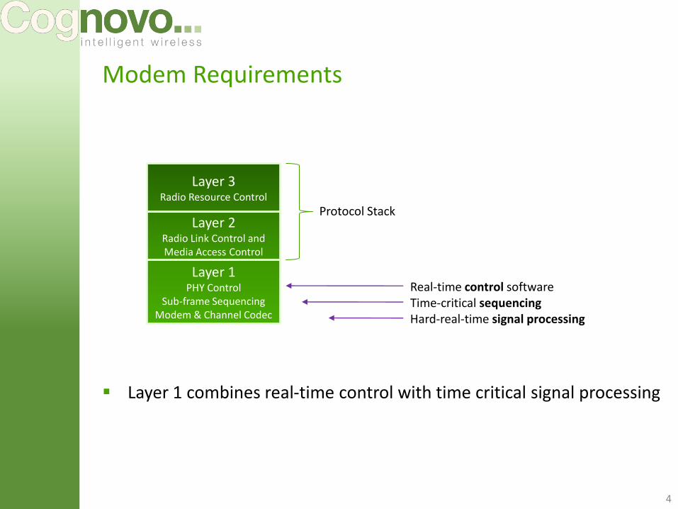
Modem Requirements
Layer 1 combines real-time control with time critical signal processing
Real-time control softwareTime-critical sequencingHard-real-time signal processing
Layer 3Radio Resource Control
Layer 2Radio Link Control and Media Access Control
Layer 1PHY Control
Sub-frame SequencingModem & Channel Codec
Protocol Stack
4
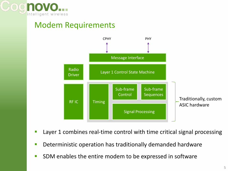
Modem Requirements
Layer 1 combines real-time control with time critical signal processing
Layer 3Radio Resource Control
Layer 2Radio Link Control and Media Access Control
Layer 1PHY Control
Sub-frame SequencingModem & Channel Codec
Message Interface
Layer 1 Control State Machine
Sub-frame Control
Sub-frame Sequences
Timing
Signal Processing
Radio Driver
RF IC
CPHY PHY
Deterministic operation has traditionally demanded hardware
SDM enables the entire modem to be expressed in software
5
Timing
Sub-frame Sequences
Signal Processing
Message Interface
Layer 1 Control State Machine
Sub-frame Control
Timing
Sub-frame Sequences
Signal Processing
Traditionally, customASIC hardware
Modem Compute Engine
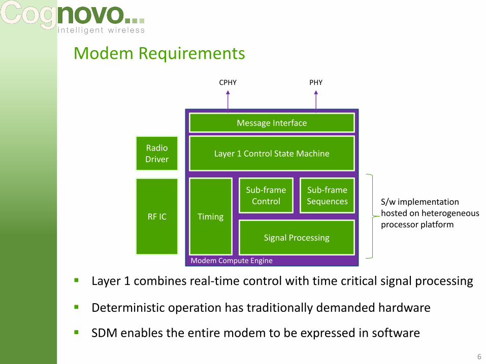
Modem Requirements
Layer 1 combines real-time control with time critical signal processing
Message Interface
Layer 1 Control State Machine
Sub-frame Control
Sub-frame Sequences
Timing
Signal Processing
Deterministic operation has traditionally demanded hardware
SDM enables the entire modem to be expressed in software
6
Timing
Sub-frame Sequences
Signal Processing
Message Interface
Layer 1 Control State Machine
Sub-frame Control
Timing
Sub-frame Sequences
Signal Processing
S/w implementationhosted on heterogeneous processor platform
Radio Driver
RF IC
CPHY PHY
A System Solution for SDM – Layer 1 Partitioning
7
Applications
SoftwareHardware
Generic s/w execution environment
Modem specific operation
Protocol Plane
Modem Compute Engine
Control Plane
Layers 2, 3, 4 Protocol
Stack
Layer 1
SDM-OS
Data Plane
PhysicalLayer
Libraries
ControlProcessor
Data Processor
Protocol Processor
System
RF
Sequence Processor
Common Infrastructure
Software Domain
The Soft Modem
External
Hardware abstraction & APICommon services
Common functionsCode re-use
Heterogeneous Multi-processing
Layer 1
RF Driver
PHY
Modem Compute Engine
ControlProcessor
Data Processor
RF
Sequence Processor
Software Domain
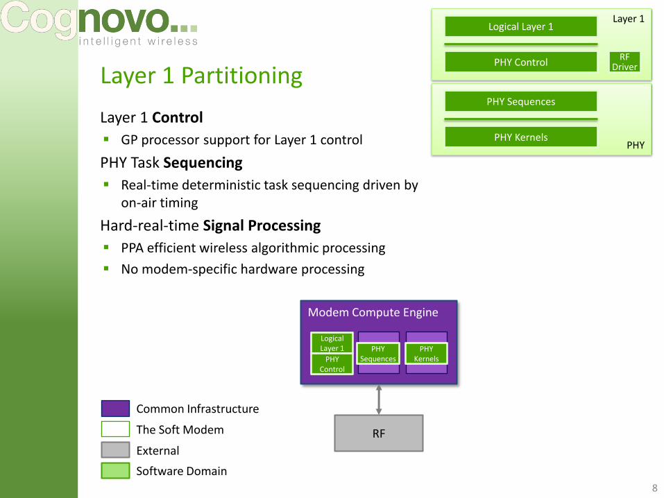
Layer 1 Partitioning
8
Logical Layer 1
PHY Control
PHY Sequences
PHY Kernels
Logical Layer 1
PHYControl
PHY Sequences
PHYKernels
Layer 1 Control
GP processor support for Layer 1 control
PHY Task Sequencing
Real-time deterministic task sequencing driven by on-air timing
Hard-real-time Signal Processing
PPA efficient wireless algorithmic processing
No modem-specific hardware processing
Common Infrastructure
The Soft Modem
External
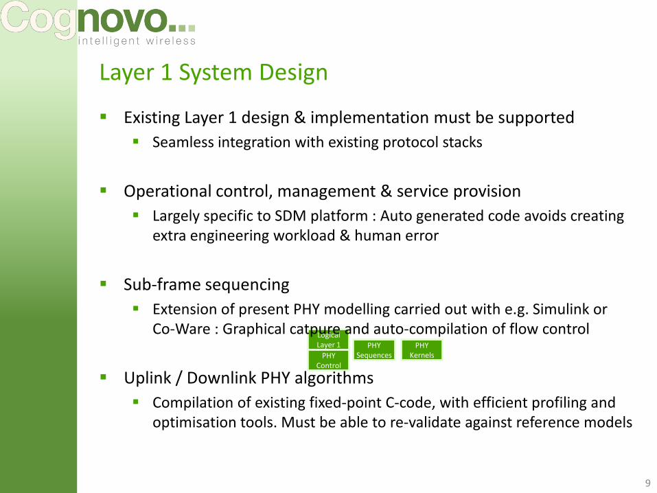
Layer 1 System Design
9
Logical Layer 1
PHYControl
PHY Sequences
PHYKernels
Existing Layer 1 design & implementation must be supported
Seamless integration with existing protocol stacks
Operational control, management & service provision
Largely specific to SDM platform : Auto generated code avoids creating extra engineering workload & human error
Sub-frame sequencing
Extension of present PHY modelling carried out with e.g. Simulink or Co-Ware : Graphical catpure and auto-compilation of flow control
Uplink / Downlink PHY algorithms
Compilation of existing fixed-point C-code, with efficient profiling and optimisation tools. Must be able to re-validate against reference models
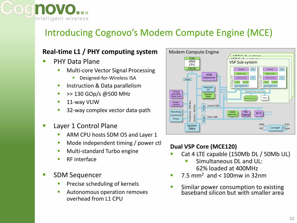
Introducing Cognovo’s Modem Compute Engine (MCE)
Real-time L1 / PHY computing system
PHY Data Plane Multi-core Vector Signal Processing
Designed-for-Wireless ISA
Instruction & Data parallelism
>> 130 GOp/s @500 MHz
11-way VLIW
32-way complex vector data-path
Layer 1 Control Plane ARM CPU hosts SDM OS and Layer 1
Mode independent timing / power ctl
Multi-standard Turbo engine
RF interface
SDM Sequencer Precise scheduling of kernels
Autonomous operation removes overhead from L1 CPU
Dual VSP Core (MCE120) Cat 4 LTE capable (150Mb DL / 50Mb UL)
Simultaneous DL and UL:62% loaded at 400MHz
7.5 mm2 and < 100mw in 32nm
Similar power consumption to existing baseband silicon but with smaller area
10
SystemRAM
InterruptCtl
Timingand Slow
Clock Unit
Power Control
Watchdog
Timers
FEC Engine RF IF
Control 32b
Data 128b
Pe
rip
he
ral –
AP
B B
us
Syst
em
–A
XI B
us
Modem Compute Engine
SystemDMA
HARQ Memory
Coresight
ARM JTAG
TraceVSP
SDM Sequencer
Bri
dge
Bri
dge
Bridge
TCMARM CPU
CACHE
VSP Sub-system
Shared Memory VDMA
Multilayer Vector Interconnect
Datapath
Register bank
DBG
CTL
Ard
beg
VSP VLIW Controller
I-TCM D-TCM
Bus Interface Unit
Datapath
Register bank
DBG
CTL
Ard
beg
VSP VLIW Controller
I-TCM D-TCM
Bus Interface Unit
VSP Sub-system
Shared Memory VDMA
Multilayer Vector Interconnect
Datapath
Register bank
DBG
CTL
Ard
beg
VSP VLIW Controller
I-TCM D-TCM
Bus Interface Unit
Datapath
Register bank
DBG
CTL
Ard
beg
VSP VLIW Controller
I-TCM D-TCM
Bus Interface Unit
VSP Sub-system
Shared Memory VDMA
Multilayer Vector Interconnect
Datapath
Register bank
DBG
CTL
Ard
beg
VSP VLIW Controller
I-TCM D-TCM
Bus Interface Unit
Datapath
Register bank
DBG
CTL
Ard
beg
VSP VLIW Controller
I-TCM D-TCM
Bus Interface Unit
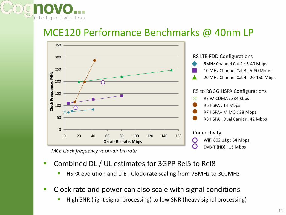
MCE120 Performance Benchmarks @ 40nm LP
Combined DL / UL estimates for 3GPP Rel5 to Rel8 HSPA evolution and LTE : Clock-rate scaling from 75MHz to 300MHz
Clock rate and power can also scale with signal conditions High SNR (light signal processing) to low SNR (heavy signal processing)
11
0
50
100
150
200
250
300
350
0 20 40 60 80 100 120 140 160
Clo
ck F
req
ue
ncy
, MH
z
On-air Bit-rate, Mbps
R8 LTE-FDD Configurations
5MHz Channel Cat 2 : 5-40 Mbps
10 MHz Channel Cat 3 : 5-80 Mbps
20 MHz Channel Cat 4 : 20-150 Mbps
R5 to R8 3G HSPA Configurations
R5 W-CDMA : 384 Kbps
R6 HSPA : 14 Mbps
R7 HSPA+ MIMO : 28 Mbps
R8 HSPA+ Dual Carrier : 42 Mbps
Connectivity
WiFi 802.11g : 54 Mbps
DVB-T (HD) : 15 MbpsMCE clock frequency vs on-air bit-rate
11
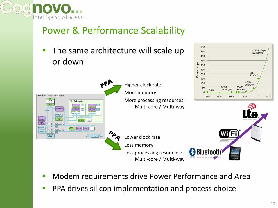
Power & Performance Scalability
The same architecture will scale up or down
12
SystemRAM
InterruptCtl
Timingand Slow
Clock Unit
Power Control
Watchdog
Timers
Turbo RF IF
Control 32b
Data 128b
Pe
rip
he
ral –
AP
B B
us
Sy
ste
m –
AX
I B
us
Modem Compute Engine
SystemDMA
HARQ Memory
Coresight
ARM JTAG
TraceVSP
VSP Sub-system
Shared Memory VDMA
Multilayer Vector Interconnect
Datapath
Register bank
DBG
CTL
Ard
be
g V
SP
VLIW Controller
I-TCM D-TCM
Bus Interface Unit
Datapath
Register bank
DBG
CTL
Ard
be
g V
SP
VLIW Controller
I-TCM D-TCM
Bus Interface Unit
Sequencer
Bri
dge
Bri
dge
Bridge
TCMARM CPU
CACHE
Higher clock rate
More memory
More processing resources: Multi-core / Multi-way
Lower clock rate
Less memory
Less processing resources: Multi-core / Multi-way
0
50
100
150
200
250
300
350
400
450
500
1990 1995 2000 2005 2010 2015
Bitra
te, M
bp
s
GSM
GPRS
200MOp/s
HSPA
5GOp/s
LTE
50GOp/s
LTE-A 1Gbps
300GOp/s
HSPA+
20GOp/s
Modem requirements drive Power Performance and Area
PPA drives silicon implementation and process choice
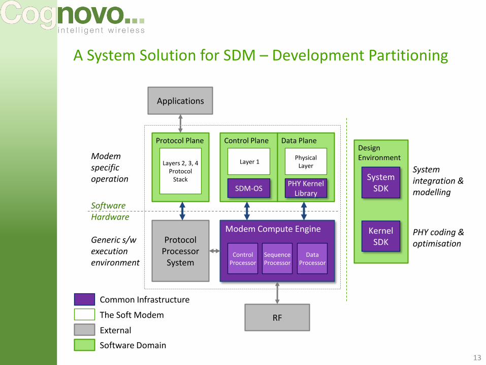
A System Solution for SDM – Development Partitioning
13
Applications
SoftwareHardware
Generic s/w execution environment
Modem specific operation
Protocol Plane
Modem Compute Engine
Control Plane
Layers 2, 3, 4 Protocol
Stack
Layer 1
SDM-OS
Data Plane
PhysicalLayer
PHY Kernel Library
ControlProcessor
Data Processor
Protocol Processor
System
RF
Sequence Processor
PHY coding & optimisation
Design Environment
System SDK
KernelSDK
System integration & modelling
Software Domain
Common Infrastructure
The Soft Modem
External
Layer 1
RF Driver
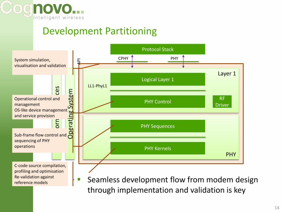
Development Partitioning
14
Op
erat
ing
Syst
em
Protocol Stack
Logical Layer 1
CPHY PHY
PHY Control
LL1-PhyL1
PHY
PHY Sequences
PHY Kernels
Pla
tfo
rm R
eso
urc
es
AP
I
C-code source compilation, profiling and optimisationRe-validation against reference models
Sub-frame flow control and sequencing of PHY operations
Operational control and managementOS-like device management and service provision
System simulation, visualisation and validation
Seamless development flow from modem design through implementation and validation is key
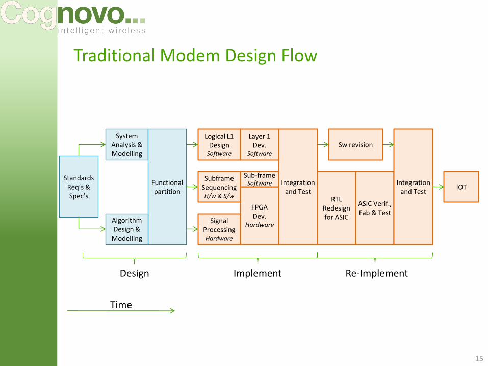
Traditional Modem Design Flow
System Analysis & Modelling
Functionalpartition
FPGA Dev.
Hardware
Layer 1 Dev.
Software
Integration and Test
RTLRedesignfor ASIC
Sw revision
IOT
Algorithm Design &
Modelling
Logical L1 Design
Software
SubframeSequencing H/w & S/w
Signal Processing Hardware
Standards Req’s & Spec’s
ASIC Verif., Fab & Test
Integration and Test
Sub-frameSoftware
Design Implement Re-Implement
Time
15
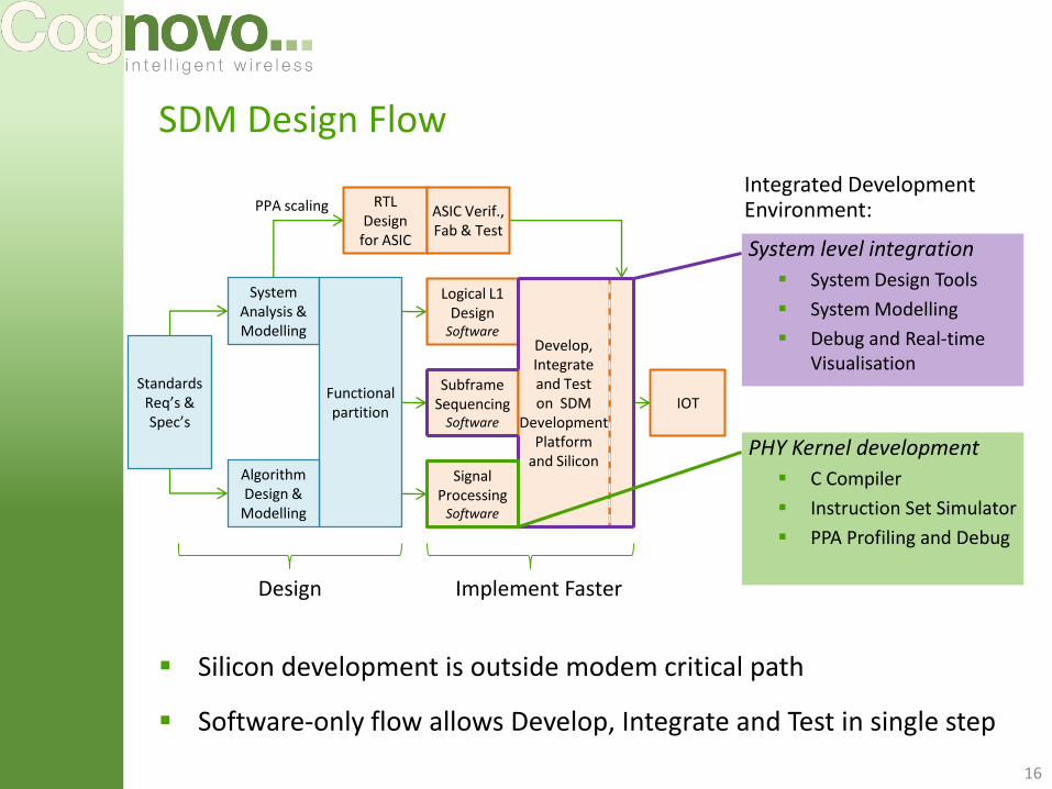
SDM Design Flow
Logical L1 Design
Software
SubframeSequencing
Software
Signal Processing
Software
IOT
Develop, Integrate and Test on SDM
Development Platform
and Silicon
System Analysis & Modelling
Functionalpartition
Algorithm Design &
Modelling
Standards Req’s & Spec’s
RTLDesign
for ASIC
ASIC Verif., Fab & Test
Design Implement Faster
PPA scaling
Silicon development is outside modem critical path
Software-only flow allows Develop, Integrate and Test in single step
System level integration
System Design Tools
System Modelling
Debug and Real-time Visualisation
Integrated Development Environment:
PHY Kernel development
C Compiler
Instruction Set Simulator
PPA Profiling and Debug
16
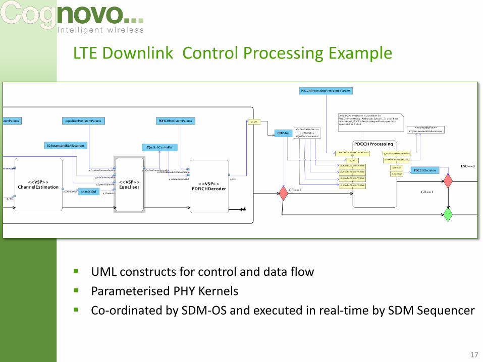
LTE Downlink Control Processing Example
UML constructs for control and data flow
Parameterised PHY Kernels
Co-ordinated by SDM-OS and executed in real-time by SDM Sequencer
17
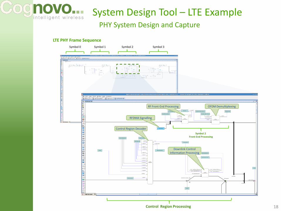
System Design Tool – LTE Example
18
RFDMA Signalling
Symbol 2 Front-End Processing
Control Region Processing
Control Region Decoder
Downlink Control Information Processing
RF Front-End Processing OFDM Demultiplexing
LTE PHY Frame Sequence
Symbol 0 Symbol 1 Symbol 2 Symbol 3
PHY System Design and Capture
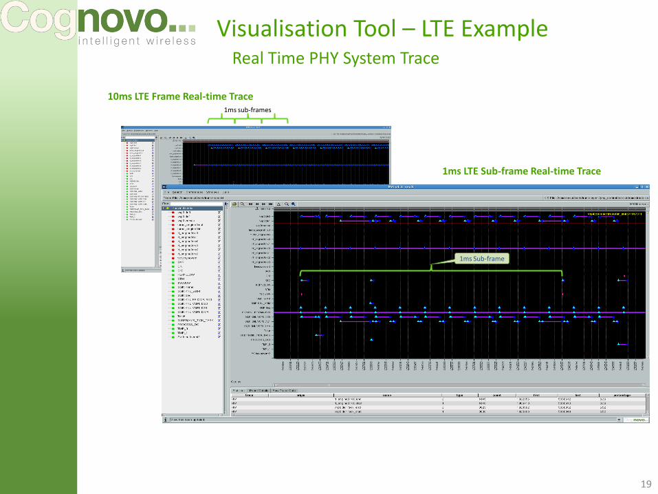
Visualisation Tool – LTE Example
19
10ms LTE Frame Real-time Trace
1ms LTE Sub-frame Real-time Trace
1ms sub-frames
1ms Sub-frame
Real Time PHY System Trace
Conclusion
Strong demand for a new approach to wireless product development Faster : Time to market
Flexibility : Single solution for multiple products, markets and standards
Smaller : Cost of development and cost of product
However, there must be no penalty Existing products must be met or bettered : Power / Cost / Size
Legacy investment maintained : e.g. Protocol stack software / multi-mode
Seamless design flow
SDM can deliver on all of these factors Heterogeneous task optimised processing
Highly parallel architecture for scalability
Whole System approach to power management , programming and debug
Control / Real-time scheduling / Data processing
20