Embed Size (px)
Citation preview
MOS –AK workshop, Silicon Valley
December 6th, 2017
Dr. Ionut RADU Director, R&D
SOITEC
SOI technology platforms for 5G:
Opportunities of collaboration
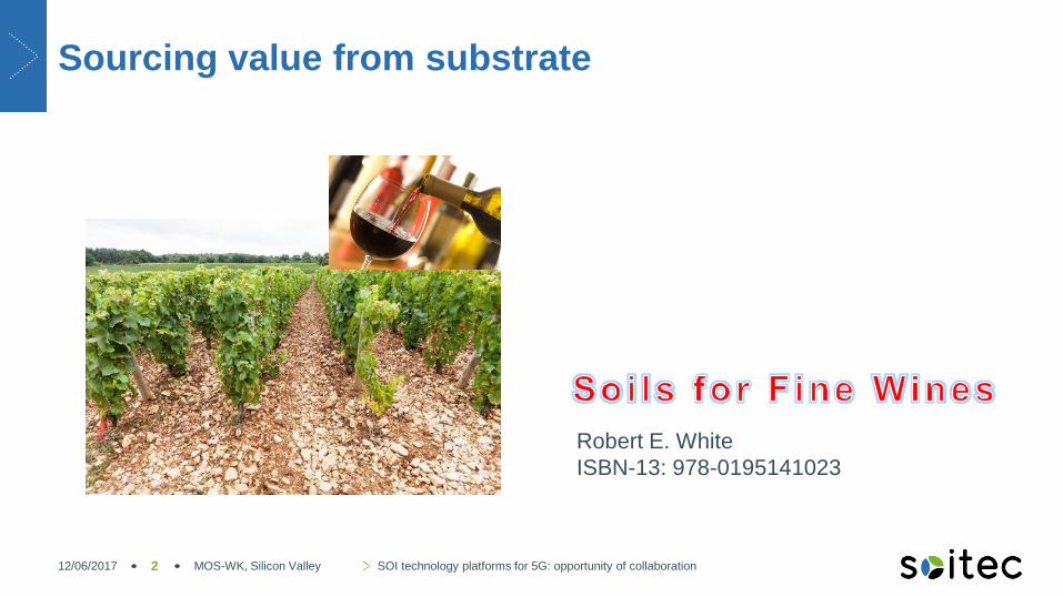
Sourcing value from substrate
MOS-WK, Silicon Valley SOI technology platforms for 5G: opportunity of collaboration 2
Robert E. White
ISBN-13: 978-0195141023
12/06/2017

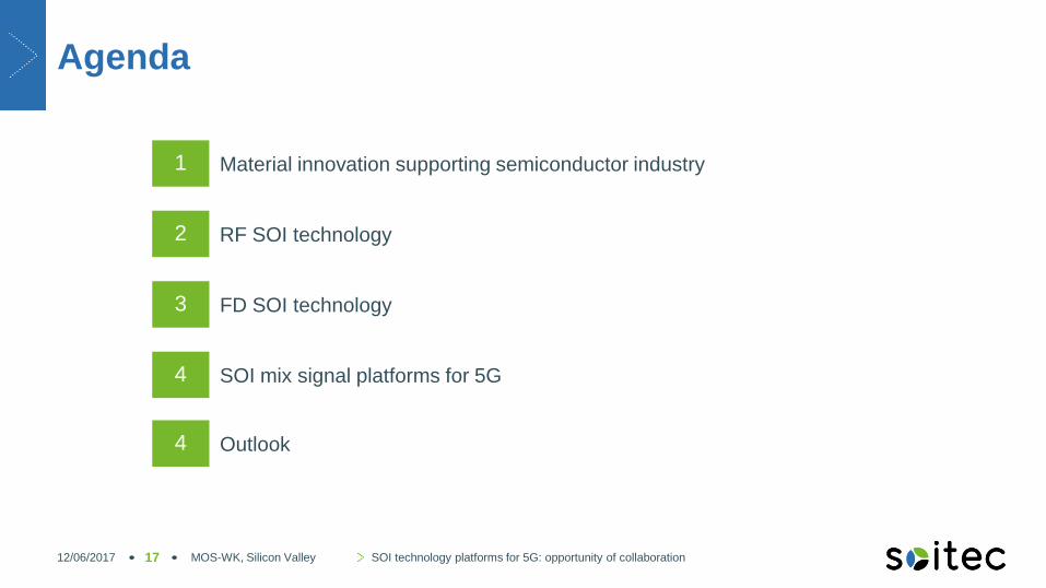
Agenda
MOS-WK, Silicon Valley SOI technology platforms for 5G: opportunity of collaboration 3
1 Material innovation supporting semiconductor industry
4 SOI mix signal platforms for 5G
2 RF SOI technology
3 FD SOI technology
4 Outlook
12/06/2017
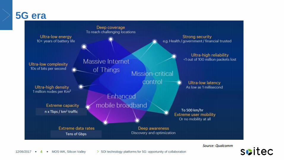
5G era
4 MOS-WK, Silicon Valley SOI technology platforms for 5G: opportunity of collaboration 12/06/2017
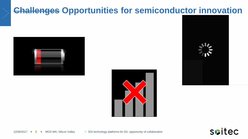
Challenges Opportunities for semiconductor innovation
MOS-WK, Silicon Valley SOI technology platforms for 5G: opportunity of collaboration 5 12/06/2017
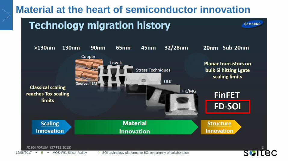
Material at the heart of semiconductor innovation
MOS-WK, Silicon Valley SOI technology platforms for 5G: opportunity of collaboration 6 12/06/2017
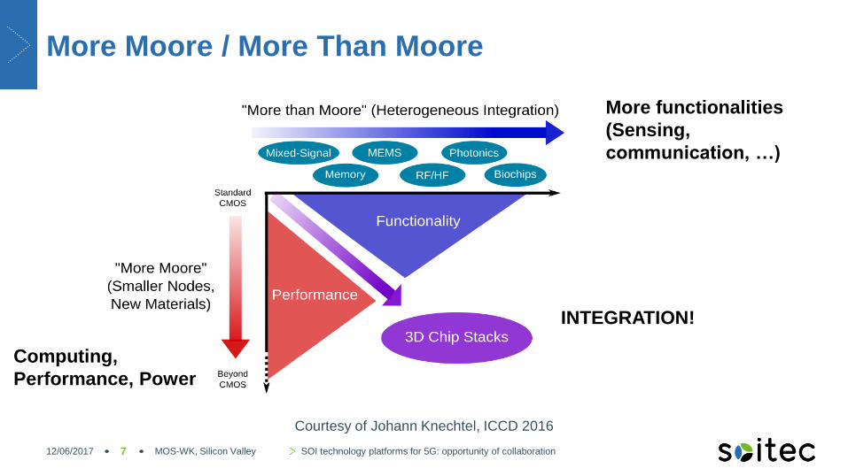
More Moore / More Than Moore
MOS-WK, Silicon Valley SOI technology platforms for 5G: opportunity of collaboration 7
Courtesy of Johann Knechtel, ICCD 2016
More functionalities
(Sensing,
communication, …)
Computing,
Performance, Power
INTEGRATION!
12/06/2017
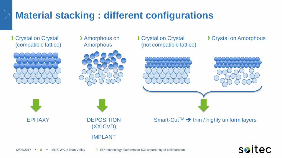
Material stacking : different configurations
Crystal on Crystal
(compatible lattice)
MOS-WK, Silicon Valley SOI technology platforms for 5G: opportunity of collaboration 8
Amorphous on
Amorphous
Crystal on Crystal
(not compatible lattice)
Crystal on Amorphous
EPITAXY DEPOSITION
(XX-CVD)
IMPLANT
Smart-CutTM thin / highly uniform layers
12/06/2017
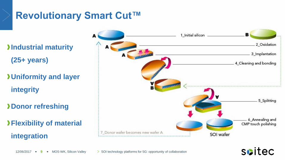
Revolutionary Smart Cut™
Industrial maturity
(25+ years)
Uniformity and layer
integrity
Donor refreshing
Flexibility of material
integration
MOS-WK, Silicon Valley SOI technology platforms for 5G: opportunity of collaboration 9 12/06/2017
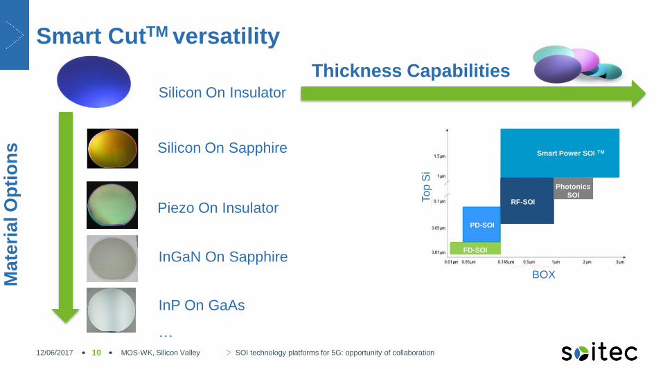
Smart CutTM versatility
Piezo On Insulator
MOS-WK, Silicon Valley SOI technology platforms for 5G: opportunity of collaboration 10
Silicon On Sapphire
InGaN On Sapphire
Ma
teri
al O
pti
on
s
Thickness Capabilities Silicon On Insulator
Top Silicon
Base Silicon
Buried Oxide
RF-SOI
Photonics
SOI
FD-SOI
Smart Power SOI TM
PD-SOI
BOX
To
p S
i
InP On GaAs
…
12/06/2017

Engineered substrates supporting our daily drivers
MOS-WK, Silicon Valley SOI technology platforms for 5G: opportunity of collaboration 11 12/06/2017

Agenda
MOS-WK, Silicon Valley SOI technology platforms for 5G: opportunity of collaboration 12
1 Material innovation supporting semiconductor industry
4 SOI mix signal platforms for 5G
2 RF SOI technology
3 FD SOI technology
4 Outlook
12/06/2017
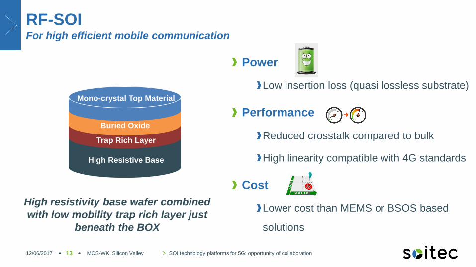
RF-SOI For high efficient mobile communication
Power
Low insertion loss (quasi lossless substrate)
Performance
Reduced crosstalk compared to bulk
High linearity compatible with 4G standards
Cost
Lower cost than MEMS or BSOS based
solutions
MOS-WK, Silicon Valley SOI technology platforms for 5G: opportunity of collaboration 13
High resistivity base wafer combined
with low mobility trap rich layer just
beneath the BOX
Mono-crystal Top Material
Buried Oxide
High Resistive Base
Trap Rich Layer
12/06/2017
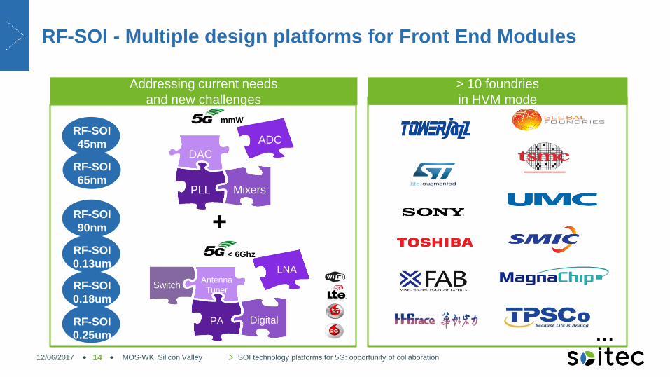
RF-SOI - Multiple design platforms for Front End Modules
14
…
> 10 foundries
in HVM mode
mmW
Switch Antenna
Tuner
LNA
PA Digital
DAC
ADC
PLL Mixers
+
RF-SOI
0.25um
RF-SOI
0.18um
RF-SOI
0.13um
RF-SOI
90nm
RF-SOI
65nm
RF-SOI
45nm
Addressing current needs
and new challenges
< 6Ghz
MOS-WK, Silicon Valley SOI technology platforms for 5G: opportunity of collaboration 12/06/2017
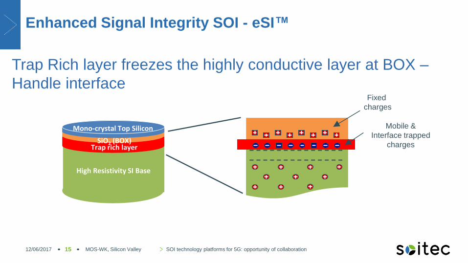
Enhanced Signal Integrity SOI - eSI™
Trap Rich layer freezes the highly conductive layer at BOX –
Handle interface
High Resistivity SI Base
Trap rich layer SiO2 (BOX)
Mono-crystal Top Silicon
Fixed
charges
Mobile &
Interface trapped
charges
MOS-WK, Silicon Valley SOI technology platforms for 5G: opportunity of collaboration 15 12/06/2017
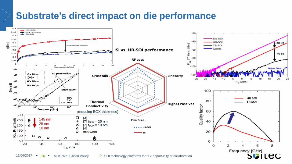
Substrate’s direct impact on die performance
RF Loss
Linearity
High Q Passives
Die Size
Thermal Conductivity
Crosstalk
eSI vs. HR-SOI performance
HR-SOI
eSI
(reducing BOX thickness) (reducing BOX thickness)
145 nm
25 nm
10 nm
MOS-WK, Silicon Valley SOI technology platforms for 5G: opportunity of collaboration 16 12/06/2017
Agenda
MOS-WK, Silicon Valley SOI technology platforms for 5G: opportunity of collaboration 17
1 Material innovation supporting semiconductor industry
4 SOI mix signal platforms for 5G
2 RF SOI technology
3 FD SOI technology
4 Outlook
12/06/2017
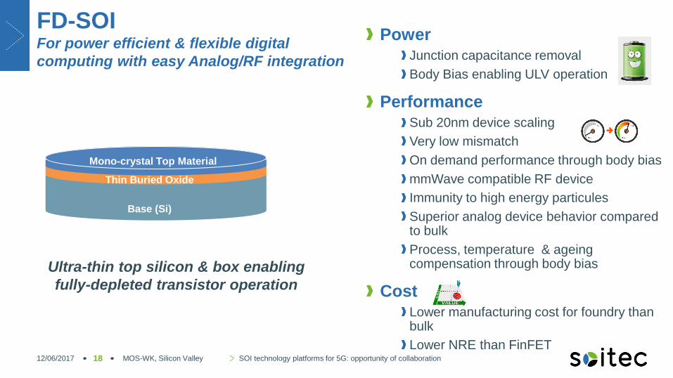
FD-SOI For power efficient & flexible digital
computing with easy Analog/RF integration
Power Junction capacitance removal
Body Bias enabling ULV operation
Performance Sub 20nm device scaling
Very low mismatch
On demand performance through body bias
mmWave compatible RF device
Immunity to high energy particules
Superior analog device behavior compared to bulk
Process, temperature & ageing compensation through body bias
Cost Lower manufacturing cost for foundry than bulk
Lower NRE than FinFET MOS-WK, Silicon Valley SOI technology platforms for 5G: opportunity of collaboration 18
Ultra-thin top silicon & box enabling
fully-depleted transistor operation
Thin Buried Oxide
Base (Si)
Mono-crystal Top Material
12/06/2017
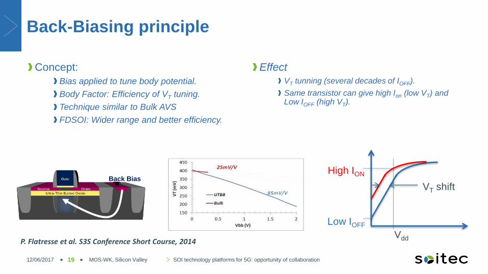
Back-Biasing principle
Concept:
Bias applied to tune body potential.
Body Factor: Efficiency of VT tuning.
Technique similar to Bulk AVS
FDSOI: Wider range and better efficiency.
Effect
VT tunning (several decades of IOFF).
Same transistor can give high Ion (low VT) and Low IOFF (high VT).
High ION
Low IOFF
Vdd
VT shift Back Bias
19
P. Flatresse et al. S3S Conference Short Course, 2014
MOS-WK, Silicon Valley SOI technology platforms for 5G: opportunity of collaboration 12/06/2017
Leakage limit
IDD
Q
SS
FF
Trimmed
Untrimmed
IDD
Q B
BG
EN
@ E
WS
/Ro
om
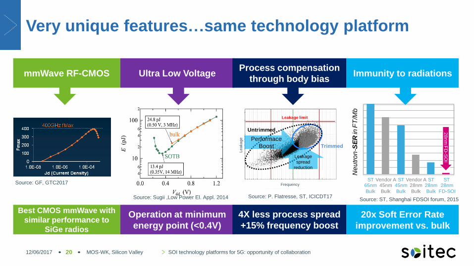
Source: P. Flatresse, ST, ICICDT17
Le
aka
ge
Frequency
Performace
Boost
Leakage
spread
reduction
Source: GF, GTC2017
Source: Sugii ,Low Power El. Appl. 2014
Ne
utr
on
-SE
Rin
FT
/Mb
28
nm
FD
-SO
I
ST65nm
Bulk
Vendor A45nm
Bulk
ST45nm
Bulk
Vendor A28nm
Bulk
ST28nm
Bulk
ST28nm
FD-SOI
Source: ST, Shanghai FDSOI forum, 2015
Very unique features…same technology platform
MOS-WK, Silicon Valley SOI technology platforms for 5G: opportunity of collaboration 20
mmWave RF-CMOS Ultra Low Voltage Process compensation
through body bias Immunity to radiations
Best CMOS mmWave with
similar performance to
SiGe radios
Operation at minimum
energy point (<0.4V)
4X less process spread
+15% frequency boost
20x Soft Error Rate
improvement vs. bulk
12/06/2017
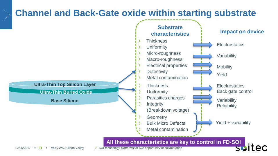
All these characteristics are key to control in FD-SOI
Channel and Back-Gate oxide within starting substrate
MOS-WK, Silicon Valley SOI technology platforms for 5G: opportunity of collaboration 21
Ultra-Thin Top Silicon Layer
Ultra-Thin Buried Oxide
Base Silicon
〉 Thickness
〉 Uniformity
〉 Parasitics charges
〉 Integrity
(Breakdown voltage)
〉 Geometry
〉 Bulk Micro Defects
〉 Metal contamination
Substrate
characteristics Impact on device
Electrostatics
Back gate control
Variability
Reliability
Yield + variability
〉 Thickness
〉 Uniformity
〉 Micro-roughness
〉 Macro-roughness
〉 Electrical properties
〉 Defectivity
〉 Metal contamination
Electrostatics
Variability
Mobility
Yield
12/06/2017
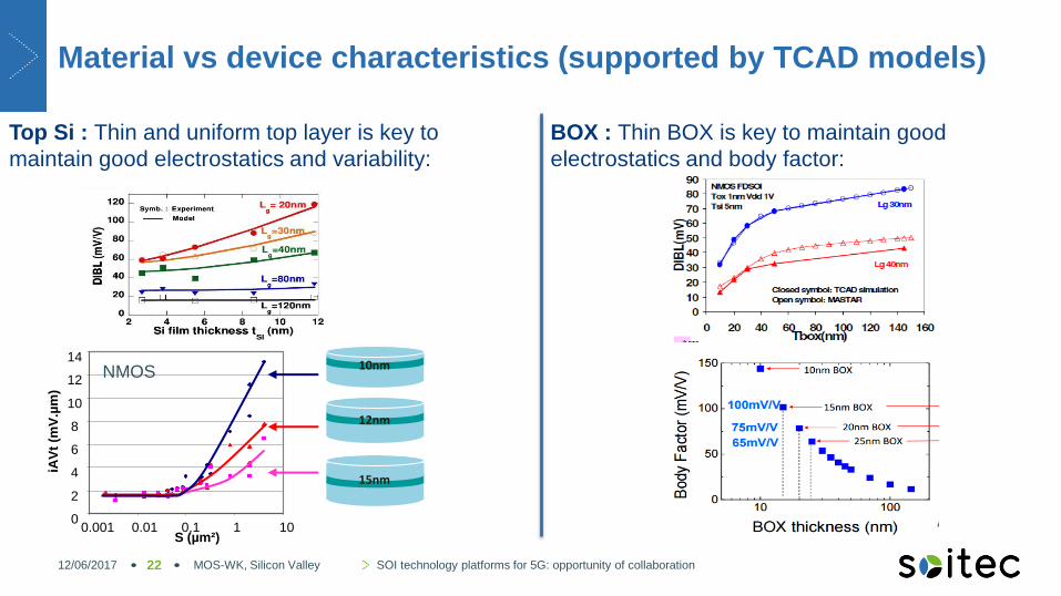
Material vs device characteristics (supported by TCAD models)
MOS-WK, Silicon Valley SOI technology platforms for 5G: opportunity of collaboration 22
wafer_1 Tsi=10nm wafer_9 Tsi=12nm wafer_17 Tsi=15nm
0
2
4
6
8
10
12
14
0.001 0.01 0.1 1 10 S (µm²)
iAV
t (m
V.µ
m)
NMOS 10nm
12nm
15nm
BOX : Thin BOX is key to maintain good
electrostatics and body factor:
Top Si : Thin and uniform top layer is key to
maintain good electrostatics and variability:
12/06/2017
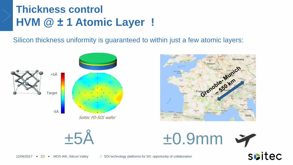
Thickness control
HVM @ ± 1 Atomic Layer !
23
Silicon thickness uniformity is guaranteed to within just a few atomic layers:
Target
+5Å
-5Å
±5Å
Soitec FD-SOI wafer
MOS-WK, Silicon Valley SOI technology platforms for 5G: opportunity of collaboration
±0.9mm 12/06/2017
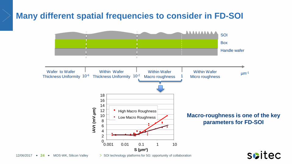
Many different spatial frequencies to consider in FD-SOI
MOS-WK, Silicon Valley SOI technology platforms for 5G: opportunity of collaboration 24
Wafer to Wafer
Thickness Uniformity
Within Wafer
Thickness Uniformity µm-1
10-6 10-2 1 Within Wafer
Macro roughness
Box
Handle wafer
SOI
Within Wafer
Micro roughness
0
2
4
6
8
10
12
14
16
18
0.001 0.01 0.1 1 10
S (µm²)
iAV
t (m
V.µ
m)
High Macro Roughness
Low Macro Roughness Macro-roughness is one of the key
parameters for FD-SOI
12/06/2017
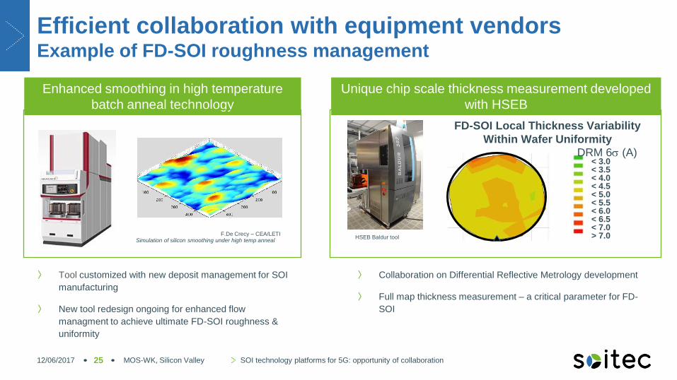
Efficient collaboration with equipment vendors Example of FD-SOI roughness management
MOS-WK, Silicon Valley SOI technology platforms for 5G: opportunity of collaboration 25
〉 Tool customized with new deposit management for SOI
manufacturing
〉 New tool redesign ongoing for enhanced flow
managment to achieve ultimate FD-SOI roughness &
uniformity
〉 Collaboration on Differential Reflective Metrology development
〉 Full map thickness measurement – a critical parameter for FD-
SOI
F.De Crecy – CEA/LETI Simulation of silicon smoothing under high temp anneal
HSEB Baldur tool
DRM 6s (A) < 3.0
< 4.0 < 4.5 < 5.0 < 5.5 < 6.0 < 6.5 < 7.0 > 7.0
< 3.5
FD-SOI Local Thickness Variability
Within Wafer Uniformity
Enhanced smoothing in high temperature
batch anneal technology
Unique chip scale thickness measurement developed
with HSEB
12/06/2017
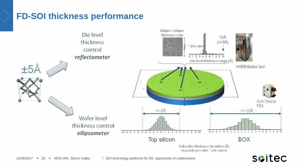
FD-SOI thickness performance
MOS-WK, Silicon Valley SOI technology platforms for 5G: opportunity of collaboration 26 12/06/2017

FD-SOI : 15nm HVM box scaling demonstrated
27 MOS-WK, Silicon Valley SOI technology platforms for 5G: opportunity of collaboration 12/06/2017
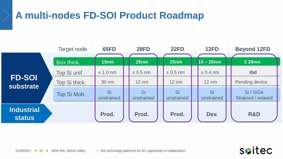
A multi-nodes FD-SOI Product Roadmap
MOS-WK, Silicon Valley SOI technology platforms for 5G: opportunity of collaboration
Top Si unif
Box thick.
Top Si Mob.
Top Si thick.
Industrial
status
FD-SOI substrate
Target node 28FD
Prod.
25nm
± 0.5 nm
12 nm
Si
unstrained
22FD
Prod.
20nm
± 0.5 nm
12 nm
Si
unstrained
Beyond 12FD
Pending device
R&D
≤ 20nm
tbd
Si / SiGe
Strained / relaxed
15 – 20nm
Si
unstrained
Dev.
± 0.4 nm
12FD
12 nm
65FD
Prod.
15nm
± 1.0 nm
30 nm
Si
unstrained
28 12/06/2017
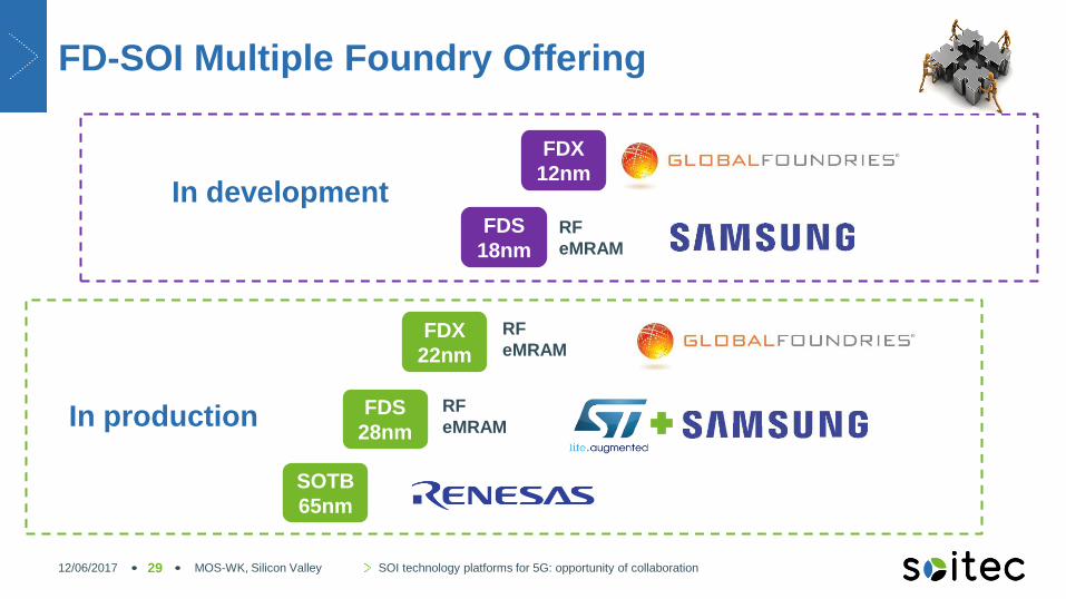
FD-SOI Multiple Foundry Offering
MOS-WK, Silicon Valley SOI technology platforms for 5G: opportunity of collaboration 29
SOTB
65nm
FDS
28nm
FDS
18nm
FDX
22nm
FDX
12nm
In production
In development
RF
eMRAM
RF
eMRAM
RF
eMRAM
12/06/2017

Accelerating FD-SOI Adoption
MOS-WK, Silicon Valley SOI technology platforms for 5G: opportunity of collaboration 30
Consumer: a game changer technology for
better battery life
Automotive : best power efficiency allowing
simpler integration and enhanced reliability
〉 FD-SOI cuts standard GPS
power consumption by 5 to 10
times
〉 i.MX reference
platform by NXP
〉Next generation e-
Cockpit solution with full
management of car
infotainment
〉FD-SOI - Reference
technology for ADAS
level 3 applications 12/06/2017

Agenda
MOS-WK, Silicon Valley SOI technology platforms for 5G: opportunity of collaboration 31
1 Material innovation supporting semiconductor industry
4 SOI mix signal platforms for 5G
2 RF SOI technology
3 FD SOI technology
4 Outlook
12/06/2017
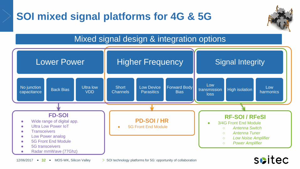
SOI mixed signal platforms for 4G & 5G
MOS-WK, Silicon Valley SOI technology platforms for 5G: opportunity of collaboration 32
Mixed signal design & integration options
Lower Power
No junction capacitance
Back Bias Ultra low
VDD
Higher Frequency
Short Channels
Low Device Parasitics
Forward Body Bias
Signal Integrity
Low transmission
loss High isolation
Low harmonics
RF-SOI / RFeSI ● 3/4G Front End Module
○ Antenna Switch
○ Antenna Tuner
○ Low Noise Amplifier
○ Power Amplifier
FD-SOI ● Wide range of digital app.
● Ultra Low Power IoT
● Transceivers
● Low Power analog
● 5G Front End Module
● 5G transceivers
● Radar mmWave (77Ghz)
PD-SOI / HR ● 5G Front End Module
12/06/2017
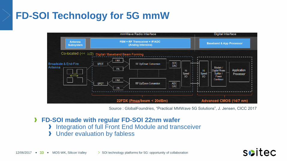
FD-SOI Technology for 5G mmW
MOS-WK, Silicon Valley SOI technology platforms for 5G: opportunity of collaboration 33
Source : GlobalFoundries, “Practical MMWave 5G Solutions”, J. Jensen, CICC 2017
FD-SOI made with regular FD-SOI 22nm wafer Integration of full Front End Module and transceiver Under evaluation by fabless
12/06/2017
Take-Aways
Engineered substrate brings value (i.e. PPAC) to device and electronic circuits
SOI substrates are enabling functionalities integration => paradigm shift
Smart Cut enables heterogeneous material integration meeting 5G
applications requirements
Close collaboration and partnership starting at early development phases
between technology developers and device and circuit modeling is mandatory to
design the 5G products
MOS-WK, Silicon Valley SOI technology platforms for 5G: opportunity of collaboration 34 12/06/2017
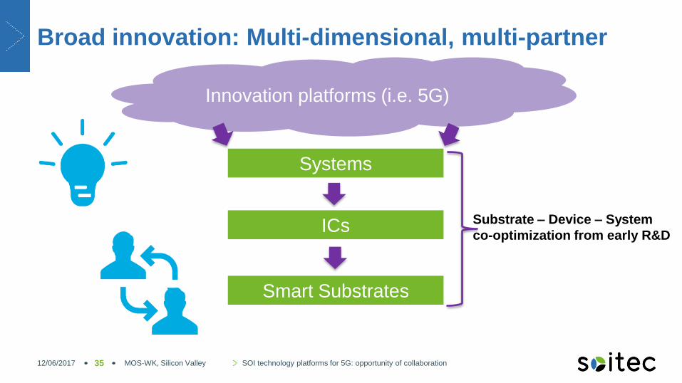
Broad innovation: Multi-dimensional, multi-partner
MOS-WK, Silicon Valley SOI technology platforms for 5G: opportunity of collaboration 35
Substrate – Device – System
co-optimization from early R&D
Innovation platforms (i.e. 5G)
Systems
ICs
Smart Substrates
12/06/2017


![Monolithic silicon-photonic platforms in state-of-the-art ... · Monolithic silicon-photonic platforms in state-of-the-art CMOS SOI processes [Invited] VLADIMIR STOJANOVIC´,1,2,*](https://img.pdfslide.net/doc/110x75/60a637b0c73a7d69b73b52dd/monolithic-silicon-photonic-platforms-in-state-of-the-art-monolithic-silicon-photonic.jpg)