Embed Size (px)
Citation preview

Spartan-6 FPGA GTP Transceivers
Advance Product Specification
UG386 (v2.2) April 30, 2010
Spartan-6 FPGA GTP Transceivers (Advance Spec) www.xilinx.com UG386 (v2.2) April 30, 2010
Xilinx is disclosing this user guide, manual, release note, and/or specification (the "Documentation") to you solely for use in the development of designs to operate with Xilinx hardware devices. You may not reproduce, distribute, republish, download, display, post, or transmit the Documentation in any form or by any means including, but not limited to, electronic, mechanical, photocopying, recording, or otherwise, without the prior written consent of Xilinx. Xilinx expressly disclaims any liability arising out of your use of the Documentation. Xilinx reserves the right, at its sole discretion, to change the Documentation without notice at any time. Xilinx assumes no obligation to correct any errors contained in the Documentation, or to advise you of any corrections or updates. Xilinx expressly disclaims any liability in connection with technical support or assistance that may be provided to you in connection with the Information.
THE DOCUMENTATION IS DISCLOSED TO YOU “AS-IS” WITH NO WARRANTY OF ANY KIND. XILINX MAKES NO OTHER WARRANTIES, WHETHER EXPRESS, IMPLIED, OR STATUTORY, REGARDING THE DOCUMENTATION, INCLUDING ANY WARRANTIES OF MERCHANTABILITY, FITNESS FOR A PARTICULAR PURPOSE, OR NONINFRINGEMENT OF THIRD-PARTY RIGHTS. IN NO EVENT WILL XILINX BE LIABLE FOR ANY CONSEQUENTIAL, INDIRECT, EXEMPLARY, SPECIAL, OR INCIDENTAL DAMAGES, INCLUDING ANY LOSS OF DATA OR LOST PROFITS, ARISING FROM YOUR USE OF THE DOCUMENTATION.
© 2009–2010 Xilinx, Inc. XILINX, the Xilinx logo, Virtex, Spartan, ISE, and other designated brands included herein are trademarks of Xilinx in the United States and other countries. PCI, PCI Express, PCIe, and PCI-X are trademarks of PCI-SIG. All other trademarks are the property of their respective owners.
Revision HistoryThe following table shows the revision history for this document.
Date Version Revision
06/24/09 1.0 Initial Xilinx release.
11/11/09 2.0 Replaced GTP_DUAL with GTPA1_DUAL throughout.
Chapter 1:
• Removed Table 1-1.• Added new section Port and Attribute Summary, page 17.• Table 1-3, page 24: Updated description of SIM_RECEIVER_DETECT_PASS attribute.• Updated Figure 1-9, page 31.• Added Figure 1-5, page 28, Figure 1-6, page 28, Figure 1-10, page 32, Figure 1-11,
page 33, Figure 1-12, page 34, Figure 1-13, page 35, and Figure 1-14, page 36.
Chapter 2:
• Added new sections Reference Clock Input Structure, page 37, and Multiple External Reference Clock Use Model, page 46.
• Added Figure 2-2, page 40.• Revised paragraphs before Figure 2-3, page 41 on reference clock multiplexer
structure.• Table 2-5, page 42: Updated descriptions of CLKINEAST, CLKINWEST, PLLCLK,
and PLLCLK ports. Added GTPCLKFBEAST, GTPCLKFBSEL0EAST, GTPCLKFBSEL0WEST, GTPCLKFBSEL1EAST, GTPCLKFBSEL1WEST, GTPCLKFBWEST, and REFCLKPWRDNB ports.
• Table 2-7, page 49: Removed TXPLL_DIVSEL_REF attribute.• Table 2-10, page 50: Renamed PCIe Optimal Jitter as PCIe Additional Margin and
added table note.• Table 2-11, page 52: Added table note (1). Updated description of GTPRESET.
Changed domains of PRBSCNTRESET and RESETDONE.• Figure 2-10, page 52: Added blocks showing falling edge of PLLPOWERDOWN0.
UG386 (v2.2) April 30, 2010 www.xilinx.com Spartan-6 FPGA GTP Transceivers (Advance Spec)
11/11/09(Cont’d)
2.0 Chapter 2 (Cont’d):
• Table 2-12, page 53: Added RX_EN_MODE_RESET_BUF_(0/1) attribute and table note.
• Revised Figure 2-11, page 54, and Figure 2-12, page 54.• Table 2-14, page 57: Added (0/1) after port names in Recommended Reset column.
Chapter 3:
• Added bullets describing GTPCLKOUT to Connecting TXUSRCLK and TXUSRCLK2, page 72.
• Added new section Using GTPCLKOUT to Drive the GTP TX, page 73.• Table 3-5, page 79: Changed Skew Reduction to TX Lane-to-Lane Deskew.• Table 3-7, page 80: Updated description of TX_BUFFER_USE.• Updated TX Buffer Bypass, page 81.• Added Figure 3-10, page 84, Figure 3-11, page 84, Figure 3-12, page 86, and
Figure 3-13, page 87.• Added Table 3-10, page 83, Table 3-11, page 85, and Table 3-12, page 85.• Table 3-22, page 98: Updated description of TXDETECTRX.• Table 3-23, page 99: Updated descriptions of RXSTATUS and TXCOMSTART.
Chapter 4:
• Updated Figure 4-2, page 102, Figure 4-3, page 105, Figure 4-4, page 104, Figure 4-4, page 106, Figure 4-5, page 107, Figure 4-6, page 108, and Figure 4-10, page 116.
• Table 4-2, page 103: Changed precision resistor value in description of TERMINATION_OVRD from 100Ω to 50Ω.
• Table 4-3, page 104: Updated RX termination voltage in rows 1 and 2.• Table 4-4, page 105: Changed internal bias from 800 mV to 900 mV.• Table 4-5, page 104: Changed term voltage from VTT to MGTVTTRX. Changed
internal bias from 800 mV to 900 mV.• Table 4-5, page 106: Changed term voltage from 2/3MGTAVTT to 3/4MGTAVTTRX.
Changed internal bias from 800 mV to 900 mV.• Table 4-6, page 107: Changed term voltage from VTT to MGTAVTTRX. Changed
internal bias from 800 mV to 900 mV.• Table 4-7, page 108: Changed term voltage from 2/3MGTAVTT to 3/4MGTAVTTRX.
Changed internal bias from 800 mV to 900 mV.• Table 4-8, page 109: Changed direction of RXVALID port from In to Out.• Table 4-9, page 109: Updated description of OOBDETECT_THRESHOLD_(0/1).• Table 4-21, page 122: Updated description of RX_PRBS_ERR_CNT_(0/1).• Table 4-22, page 125: Added RXSLIDE port.• Table 4-23, page 127: Added MCOMMA_10B_VALUE, MCOMMA_DETECT,
PCOMMA_10B_VALUE, PCOMMA_DETECT, and RX_SLIDE_MODE attributes.• Replaced RX Buffer Bypass section with RX Elastic Buffer Bypass, page 133.• Added Figure 4-22, page 137, Figure 4-23, page 138, Figure 4-24, page 139, and
Figure 4-25, page 140.• Removed RX gearbox from PCS Parallel Clock section of Figure 4-21, page 134 and
Figure 4-26, page 141.• Table 4-34, page 144: Removed RXDATAWIDTH.• Table 4-36, page 149: Updated descriptions of RXCHBONDI[2:0],
RXCHBONDO[2:0], RXCHBONDMASTER(0/1), and RXCHBONDSLAVE(0/1).
Date Version Revision
Spartan-6 FPGA GTP Transceivers (Advance Spec) www.xilinx.com UG386 (v2.2) April 30, 2010
11/11/09(Cont’d)
2.0 Chapter 4 (Cont’d):
• Table 4-37, page 151: Added attributes CB2_INH_CC_PERIOD_(0/1) and RX_EN_MODE_RESET_BUF_(0/1). Updated descriptions of CHAN_BOND_1/2_MAX_SKEW_(0/1), CHAN_BOND_KEEP_ALIGN_(0/1), and CHAN_BOND_SEQ_LEN_(0/1). Removed CHAN_BOND_SEQ_2_CFG.
• Updated Channel Bonding Mode, page 153 and step 4 in Enabling Channel Bonding, page 152.
• Updated description of RXUSRCLK and RXUSRCLK2 before Equation 4-2 in Connecting RXUSRCLK and RXUSRCLK2, page 158.
• Changed RXDATAWIDTH to 1 in Equation 4-3.• Table 4-38, page 155: Updated description of REFCLKOUT port.
Chapter 5:
• Added Overview, page 161.• Table 5-1, page 161: Added nominal voltage to descriptions of MGTAVCC,
MGTAVCCPLL0, MGTAVCCPLL1, MGTAVTTRX, and MGTAVTTTX. Updated descriptions of MGTRXP0/MGTRXN0, MGTRXP1/MGTRXN1, MGTTXP0/MGTTXN0, and MGTTXP1/MGTTXN1.
• Added Figure 5-1, page 163.• Revised Power Supply and Filtering, page 171.• Added Figure 5-11, page 174, Figure 5-12, page 175, Figure 5-13, page 176, and
Table 5-4, page 173.
Appendix B:
• Added new appendix.
03/30/10 2.1 Added PMA_CDR_SCAN_(0/1) and PMA_RX_CFG_1 to Table 1-2. Updated Figure 1-4 and description of Figure 1-6. Added Figure 1-7 and Figure 1-8. Updated device packages in Figure 1-9, Figure 1-10, Figure 1-11, Figure 1-12, Figure 1-13, and Figure 1-14.
Updated Table 2-2 and Table 2-4. Changed GTPRXRESET1 to GTPRESET1 in description of Figure 2-7. Updated REFCLK frequency for Aurora standard and added 0.6144 line rate to CPRI standard in Table 2-10.
Added note to Table 3-1. Updated Using GTPCLKOUT to Drive the GTP TX. Updated Table 3-6, Table 3-7, and Table 3-9. Updated Figure 3-12, Figure 3-13, and Figure 3-19. Updated Table 3-21.
Updated Figure 4-2. Removed Table 4-5: RX Termination Use Mode 2 Configuration and Notes, and Figure 4-4: RX Termination Use Mode 2 Configuration. Updated Table 4-5, Table 4-6, Table 4-7, Figure 4-4, Figure 4-5, and Figure 4-6. Updated descriptions of PMA_CDR_SCAN_(0/1) and PMA_RX_CFG_(0/1) in Table 4-13. Updated Horizontal Eye Margin Scan. Updated PMA_CDR_SCAN_(0/1) and added PMA_RX_CFG_(0/1) to Table 4-18. Updated Table 4-23. Updated Figure 4-18 and Functional Description. Updated Figure 4-24 and Figure 4-25. Added note to Table 4-38. Added bullet to Connecting RXUSRCLK and RXUSRCLK2.
Updated Figure 5-1 and description after Figure 5-2. Removed Signal Launch Layout Recommendation section.
04/30/10 2.2 Upated descriptions of MGTREFCLK0P/MGTREFCLK0N and MGTREFCLK1P/MGTREFCLK1N in Table 5-1. Added Table 5-2 and Table 5-3 to Managing Used and Unused GTP Transceivers. Added Signal Launch Layout Recommendations.
Date Version Revision
Spartan-6 FPGA GTP Transceivers (Advance Spec) www.xilinx.com 5UG386 (v2.2) April 30, 2010
Revision History . . . . . . . . . . . . . . . . . . . . . . . . . . . . . . . . . . . . . . . . . . . . . . . . . . . . . . . . . . . . . 2
Preface: About This GuideGuide Contents . . . . . . . . . . . . . . . . . . . . . . . . . . . . . . . . . . . . . . . . . . . . . . . . . . . . . . . . . . . . . 11Additional Documentation . . . . . . . . . . . . . . . . . . . . . . . . . . . . . . . . . . . . . . . . . . . . . . . . . . 11Additional Documentation Resources . . . . . . . . . . . . . . . . . . . . . . . . . . . . . . . . . . . . . . . 12Additional Support Resources . . . . . . . . . . . . . . . . . . . . . . . . . . . . . . . . . . . . . . . . . . . . . . . 12
Chapter 1: Transceiver and Tool OverviewOverview . . . . . . . . . . . . . . . . . . . . . . . . . . . . . . . . . . . . . . . . . . . . . . . . . . . . . . . . . . . . . . . . . . . 13Port and Attribute Summary . . . . . . . . . . . . . . . . . . . . . . . . . . . . . . . . . . . . . . . . . . . . . . . . 17Spartan-6 FPGA GTP Transceiver Wizard . . . . . . . . . . . . . . . . . . . . . . . . . . . . . . . . . . . 22Simulation . . . . . . . . . . . . . . . . . . . . . . . . . . . . . . . . . . . . . . . . . . . . . . . . . . . . . . . . . . . . . . . . . . 23
Functional Description . . . . . . . . . . . . . . . . . . . . . . . . . . . . . . . . . . . . . . . . . . . . . . . . . . . . 23Simulation-only Ports and Attributes . . . . . . . . . . . . . . . . . . . . . . . . . . . . . . . . . . . . . . . . 23
SIM_GTPRESET_SPEEDUP . . . . . . . . . . . . . . . . . . . . . . . . . . . . . . . . . . . . . . . . . . . . . . 25SIM_RECEIVER_DETECT_PASS . . . . . . . . . . . . . . . . . . . . . . . . . . . . . . . . . . . . . . . . . . 25SIM_REFCLK0_SOURCE . . . . . . . . . . . . . . . . . . . . . . . . . . . . . . . . . . . . . . . . . . . . . . . . 26SIM_REFCLK1_SOURCE . . . . . . . . . . . . . . . . . . . . . . . . . . . . . . . . . . . . . . . . . . . . . . . . 26SIM_TX_ELEC_IDLE_LEVEL. . . . . . . . . . . . . . . . . . . . . . . . . . . . . . . . . . . . . . . . . . . . . 26SIM_VERSION . . . . . . . . . . . . . . . . . . . . . . . . . . . . . . . . . . . . . . . . . . . . . . . . . . . . . . . . 26
Implementation . . . . . . . . . . . . . . . . . . . . . . . . . . . . . . . . . . . . . . . . . . . . . . . . . . . . . . . . . . . . . 26CSG324 Package Placement Diagrams . . . . . . . . . . . . . . . . . . . . . . . . . . . . . . . . . . . . . . . 28CSG484 Package Placement Diagrams . . . . . . . . . . . . . . . . . . . . . . . . . . . . . . . . . . . . . . . 29FG(G)484 Package Placement Diagrams . . . . . . . . . . . . . . . . . . . . . . . . . . . . . . . . . . . . . 31FG(G)676 Package Placement Diagrams . . . . . . . . . . . . . . . . . . . . . . . . . . . . . . . . . . . . . 33FG(G)900 Package Placement Diagrams . . . . . . . . . . . . . . . . . . . . . . . . . . . . . . . . . . . . . 35
Chapter 2: Shared Transceiver FeaturesReference Clock Input Structure . . . . . . . . . . . . . . . . . . . . . . . . . . . . . . . . . . . . . . . . . . . . . 37
Functional Description . . . . . . . . . . . . . . . . . . . . . . . . . . . . . . . . . . . . . . . . . . . . . . . . . . . . 37Ports and Attributes. . . . . . . . . . . . . . . . . . . . . . . . . . . . . . . . . . . . . . . . . . . . . . . . . . . . . . . 37Use Modes: Reference Clock Termination . . . . . . . . . . . . . . . . . . . . . . . . . . . . . . . . . . . . 38
Reference Clock Selection and Distribution . . . . . . . . . . . . . . . . . . . . . . . . . . . . . . . . . 38Functional Description . . . . . . . . . . . . . . . . . . . . . . . . . . . . . . . . . . . . . . . . . . . . . . . . . . . . 38Ports and Attributes. . . . . . . . . . . . . . . . . . . . . . . . . . . . . . . . . . . . . . . . . . . . . . . . . . . . . . . 42Single External Reference Clock Use Model . . . . . . . . . . . . . . . . . . . . . . . . . . . . . . . . . . 44Multiple External Reference Clock Use Model . . . . . . . . . . . . . . . . . . . . . . . . . . . . . . . . 46
PLL . . . . . . . . . . . . . . . . . . . . . . . . . . . . . . . . . . . . . . . . . . . . . . . . . . . . . . . . . . . . . . . . . . . . . . . . . 47Functional Description . . . . . . . . . . . . . . . . . . . . . . . . . . . . . . . . . . . . . . . . . . . . . . . . . . . . 47Ports and Attributes. . . . . . . . . . . . . . . . . . . . . . . . . . . . . . . . . . . . . . . . . . . . . . . . . . . . . . . 49PLL Settings for Common Protocols . . . . . . . . . . . . . . . . . . . . . . . . . . . . . . . . . . . . . . . . . 50
Reset. . . . . . . . . . . . . . . . . . . . . . . . . . . . . . . . . . . . . . . . . . . . . . . . . . . . . . . . . . . . . . . . . . . . . . . . 51
Table of Contents
6 www.xilinx.com Spartan-6 FPGA GTP Transceivers (Advance Spec)UG386 (v2.2) April 30, 2010
Functional Description . . . . . . . . . . . . . . . . . . . . . . . . . . . . . . . . . . . . . . . . . . . . . . . . . . . . 51Ports and Attributes. . . . . . . . . . . . . . . . . . . . . . . . . . . . . . . . . . . . . . . . . . . . . . . . . . . . . . . 52GTP Reset in Response to Completion of Configuration . . . . . . . . . . . . . . . . . . . . . . . . 54GTP Reset When the GTPRESET Port is Asserted . . . . . . . . . . . . . . . . . . . . . . . . . . . . . 54GTP Component-Level Resets . . . . . . . . . . . . . . . . . . . . . . . . . . . . . . . . . . . . . . . . . . . . . . 55Link Idle Reset Support . . . . . . . . . . . . . . . . . . . . . . . . . . . . . . . . . . . . . . . . . . . . . . . . . . . . 55Resetting the GTPA1_DUAL Tile . . . . . . . . . . . . . . . . . . . . . . . . . . . . . . . . . . . . . . . . . . . 55Examples . . . . . . . . . . . . . . . . . . . . . . . . . . . . . . . . . . . . . . . . . . . . . . . . . . . . . . . . . . . . . . . . 58
Power-up and Configuration . . . . . . . . . . . . . . . . . . . . . . . . . . . . . . . . . . . . . . . . . . . . . 58After Turning on a Reference Clock . . . . . . . . . . . . . . . . . . . . . . . . . . . . . . . . . . . . . . . . 58After Changing a Reference Clock . . . . . . . . . . . . . . . . . . . . . . . . . . . . . . . . . . . . . . . . . 58Parallel Clock Source Reset. . . . . . . . . . . . . . . . . . . . . . . . . . . . . . . . . . . . . . . . . . . . . . . 58After Remote Power-up . . . . . . . . . . . . . . . . . . . . . . . . . . . . . . . . . . . . . . . . . . . . . . . . . 58Electrical Idle Reset . . . . . . . . . . . . . . . . . . . . . . . . . . . . . . . . . . . . . . . . . . . . . . . . . . . . . 58After Connecting RXP/RXN. . . . . . . . . . . . . . . . . . . . . . . . . . . . . . . . . . . . . . . . . . . . . . 58After a TX Buffer Error . . . . . . . . . . . . . . . . . . . . . . . . . . . . . . . . . . . . . . . . . . . . . . . . . . 59After an RX Buffer Error . . . . . . . . . . . . . . . . . . . . . . . . . . . . . . . . . . . . . . . . . . . . . . . . . 59Before Channel Bonding . . . . . . . . . . . . . . . . . . . . . . . . . . . . . . . . . . . . . . . . . . . . . . . . . 59After a PRBS Error . . . . . . . . . . . . . . . . . . . . . . . . . . . . . . . . . . . . . . . . . . . . . . . . . . . . . 59
Power Down . . . . . . . . . . . . . . . . . . . . . . . . . . . . . . . . . . . . . . . . . . . . . . . . . . . . . . . . . . . . . . . . 59Functional Description . . . . . . . . . . . . . . . . . . . . . . . . . . . . . . . . . . . . . . . . . . . . . . . . . . . . 59Ports and Attributes. . . . . . . . . . . . . . . . . . . . . . . . . . . . . . . . . . . . . . . . . . . . . . . . . . . . . . . 60Generic Power-Down Capabilities . . . . . . . . . . . . . . . . . . . . . . . . . . . . . . . . . . . . . . . . . . 61
PLL Power Down . . . . . . . . . . . . . . . . . . . . . . . . . . . . . . . . . . . . . . . . . . . . . . . . . . . . . . 61TX and RX Power Down. . . . . . . . . . . . . . . . . . . . . . . . . . . . . . . . . . . . . . . . . . . . . . . . . 61
Power-Down Features for PCI Express Operation . . . . . . . . . . . . . . . . . . . . . . . . . . . . . 62Power-Down Transition Times. . . . . . . . . . . . . . . . . . . . . . . . . . . . . . . . . . . . . . . . . . . . 63
Loopback . . . . . . . . . . . . . . . . . . . . . . . . . . . . . . . . . . . . . . . . . . . . . . . . . . . . . . . . . . . . . . . . . . . 63Functional Description . . . . . . . . . . . . . . . . . . . . . . . . . . . . . . . . . . . . . . . . . . . . . . . . . . . . 63Ports and Attributes. . . . . . . . . . . . . . . . . . . . . . . . . . . . . . . . . . . . . . . . . . . . . . . . . . . . . . . 64
Dynamic Reconfiguration Port . . . . . . . . . . . . . . . . . . . . . . . . . . . . . . . . . . . . . . . . . . . . . . 64Functional Description . . . . . . . . . . . . . . . . . . . . . . . . . . . . . . . . . . . . . . . . . . . . . . . . . . . . 64Ports and Attributes. . . . . . . . . . . . . . . . . . . . . . . . . . . . . . . . . . . . . . . . . . . . . . . . . . . . . . . 64
Chapter 3: TransmitterTX Overview . . . . . . . . . . . . . . . . . . . . . . . . . . . . . . . . . . . . . . . . . . . . . . . . . . . . . . . . . . . . . . . . 67FPGA TX Interface . . . . . . . . . . . . . . . . . . . . . . . . . . . . . . . . . . . . . . . . . . . . . . . . . . . . . . . . . . 68
Functional Description . . . . . . . . . . . . . . . . . . . . . . . . . . . . . . . . . . . . . . . . . . . . . . . . . . . . 68Ports and Attributes. . . . . . . . . . . . . . . . . . . . . . . . . . . . . . . . . . . . . . . . . . . . . . . . . . . . . . . 68Description . . . . . . . . . . . . . . . . . . . . . . . . . . . . . . . . . . . . . . . . . . . . . . . . . . . . . . . . . . . . . . 70
Configuring the Width of the Interface. . . . . . . . . . . . . . . . . . . . . . . . . . . . . . . . . . . . . . 70Connecting TXUSRCLK and TXUSRCLK2 . . . . . . . . . . . . . . . . . . . . . . . . . . . . . . . . . . . 72
Using GTPCLKOUT to Drive the GTP TX . . . . . . . . . . . . . . . . . . . . . . . . . . . . . . . . . . . . 73GTPCLKOUT Driving a GTP TX in 1-Byte Mode . . . . . . . . . . . . . . . . . . . . . . . . . . . . . . 73GTPCLKOUT Driving a GTP TX in 2-Byte Mode . . . . . . . . . . . . . . . . . . . . . . . . . . . . . . 74GTPCLKOUT Driving a GTP TX in 4-Byte Mode . . . . . . . . . . . . . . . . . . . . . . . . . . . . . . 74
TX 8B/10B Encoder . . . . . . . . . . . . . . . . . . . . . . . . . . . . . . . . . . . . . . . . . . . . . . . . . . . . . . . . . . 75Functional Description . . . . . . . . . . . . . . . . . . . . . . . . . . . . . . . . . . . . . . . . . . . . . . . . . . . . 75
8B/10B Bit and Byte Ordering . . . . . . . . . . . . . . . . . . . . . . . . . . . . . . . . . . . . . . . . . . . . 75K Characters . . . . . . . . . . . . . . . . . . . . . . . . . . . . . . . . . . . . . . . . . . . . . . . . . . . . . . . . . . 76Running Disparity . . . . . . . . . . . . . . . . . . . . . . . . . . . . . . . . . . . . . . . . . . . . . . . . . . . . . 76
Ports and Attributes. . . . . . . . . . . . . . . . . . . . . . . . . . . . . . . . . . . . . . . . . . . . . . . . . . . . . . . 77
Spartan-6 FPGA GTP Transceivers (Advance Spec) www.xilinx.com 7UG386 (v2.2) April 30, 2010
Enabling and Disabling 8B/10B Encoding . . . . . . . . . . . . . . . . . . . . . . . . . . . . . . . . . . . . 78TX Buffer . . . . . . . . . . . . . . . . . . . . . . . . . . . . . . . . . . . . . . . . . . . . . . . . . . . . . . . . . . . . . . . . . . . 78
Functional Description . . . . . . . . . . . . . . . . . . . . . . . . . . . . . . . . . . . . . . . . . . . . . . . . . . . . 78Ports and Attributes. . . . . . . . . . . . . . . . . . . . . . . . . . . . . . . . . . . . . . . . . . . . . . . . . . . . . . . 79Using the TX Buffer . . . . . . . . . . . . . . . . . . . . . . . . . . . . . . . . . . . . . . . . . . . . . . . . . . . . . . . 80
TX Buffer Bypass . . . . . . . . . . . . . . . . . . . . . . . . . . . . . . . . . . . . . . . . . . . . . . . . . . . . . . . . . . . 81Functional Description . . . . . . . . . . . . . . . . . . . . . . . . . . . . . . . . . . . . . . . . . . . . . . . . . . . . 81Ports and Attributes. . . . . . . . . . . . . . . . . . . . . . . . . . . . . . . . . . . . . . . . . . . . . . . . . . . . . . . 81Using the TX Phase-Alignment Circuit to Bypass the TX Buffer . . . . . . . . . . . . . . . . . 83Using the TX Phase-Alignment Circuit to Minimize TX Lane-to-Lane Skew. . . . . . . 84Using the Feedback Path to Compensate for Voltage and Temperature. . . . . . . . . . . 84
TX Pattern Generator . . . . . . . . . . . . . . . . . . . . . . . . . . . . . . . . . . . . . . . . . . . . . . . . . . . . . . . . 88Functional Description . . . . . . . . . . . . . . . . . . . . . . . . . . . . . . . . . . . . . . . . . . . . . . . . . . . . 88Ports and Attributes. . . . . . . . . . . . . . . . . . . . . . . . . . . . . . . . . . . . . . . . . . . . . . . . . . . . . . . 89Use Models . . . . . . . . . . . . . . . . . . . . . . . . . . . . . . . . . . . . . . . . . . . . . . . . . . . . . . . . . . . . . . 90
TX Polarity Control . . . . . . . . . . . . . . . . . . . . . . . . . . . . . . . . . . . . . . . . . . . . . . . . . . . . . . . . . 91Functional Description . . . . . . . . . . . . . . . . . . . . . . . . . . . . . . . . . . . . . . . . . . . . . . . . . . . . 91Ports and Attributes. . . . . . . . . . . . . . . . . . . . . . . . . . . . . . . . . . . . . . . . . . . . . . . . . . . . . . . 91Using TX Polarity Control . . . . . . . . . . . . . . . . . . . . . . . . . . . . . . . . . . . . . . . . . . . . . . . . . 91
TX Fabric Clock Output Control . . . . . . . . . . . . . . . . . . . . . . . . . . . . . . . . . . . . . . . . . . . . . 91Functional Description . . . . . . . . . . . . . . . . . . . . . . . . . . . . . . . . . . . . . . . . . . . . . . . . . . . . 91
Serial Clock Divider . . . . . . . . . . . . . . . . . . . . . . . . . . . . . . . . . . . . . . . . . . . . . . . . . . . . 92Parallel Clock Divider and Selector . . . . . . . . . . . . . . . . . . . . . . . . . . . . . . . . . . . . . . . . 93
Ports and Attributes. . . . . . . . . . . . . . . . . . . . . . . . . . . . . . . . . . . . . . . . . . . . . . . . . . . . . . . 93TX Configurable Driver . . . . . . . . . . . . . . . . . . . . . . . . . . . . . . . . . . . . . . . . . . . . . . . . . . . . . 94
Functional Description . . . . . . . . . . . . . . . . . . . . . . . . . . . . . . . . . . . . . . . . . . . . . . . . . . . . 94Ports and Attributes. . . . . . . . . . . . . . . . . . . . . . . . . . . . . . . . . . . . . . . . . . . . . . . . . . . . . . . 95Use Modes – TX Driver . . . . . . . . . . . . . . . . . . . . . . . . . . . . . . . . . . . . . . . . . . . . . . . . . . . . 96
General . . . . . . . . . . . . . . . . . . . . . . . . . . . . . . . . . . . . . . . . . . . . . . . . . . . . . . . . . . . . . . 96Use Mode – Resistor Calibration . . . . . . . . . . . . . . . . . . . . . . . . . . . . . . . . . . . . . . . . . . . . 96
TX Receiver Detect Support for PCI Express Designs . . . . . . . . . . . . . . . . . . . . . . . . 97Functional Description . . . . . . . . . . . . . . . . . . . . . . . . . . . . . . . . . . . . . . . . . . . . . . . . . . . . 97Ports and Attributes. . . . . . . . . . . . . . . . . . . . . . . . . . . . . . . . . . . . . . . . . . . . . . . . . . . . . . . 97
TX Out-of-Band Signaling. . . . . . . . . . . . . . . . . . . . . . . . . . . . . . . . . . . . . . . . . . . . . . . . . . . 99Functional Description . . . . . . . . . . . . . . . . . . . . . . . . . . . . . . . . . . . . . . . . . . . . . . . . . . . . 99Ports and Attributes. . . . . . . . . . . . . . . . . . . . . . . . . . . . . . . . . . . . . . . . . . . . . . . . . . . . . . . 99
Chapter 4: ReceiverRX Overview. . . . . . . . . . . . . . . . . . . . . . . . . . . . . . . . . . . . . . . . . . . . . . . . . . . . . . . . . . . . . . . 101RX Analog Front End . . . . . . . . . . . . . . . . . . . . . . . . . . . . . . . . . . . . . . . . . . . . . . . . . . . . . . . 102
Functional Description . . . . . . . . . . . . . . . . . . . . . . . . . . . . . . . . . . . . . . . . . . . . . . . . . . . 102Ports and Attributes. . . . . . . . . . . . . . . . . . . . . . . . . . . . . . . . . . . . . . . . . . . . . . . . . . . . . . 103Use Modes – RX Termination . . . . . . . . . . . . . . . . . . . . . . . . . . . . . . . . . . . . . . . . . . . . . 104Use Mode – Resistor Calibration . . . . . . . . . . . . . . . . . . . . . . . . . . . . . . . . . . . . . . . . . . . 108
RX Out-of-Band Signaling . . . . . . . . . . . . . . . . . . . . . . . . . . . . . . . . . . . . . . . . . . . . . . . . . 109Functional Description . . . . . . . . . . . . . . . . . . . . . . . . . . . . . . . . . . . . . . . . . . . . . . . . . . . 109Ports and Attributes. . . . . . . . . . . . . . . . . . . . . . . . . . . . . . . . . . . . . . . . . . . . . . . . . . . . . . 109
RX Equalizer . . . . . . . . . . . . . . . . . . . . . . . . . . . . . . . . . . . . . . . . . . . . . . . . . . . . . . . . . . . . . . . 111Functional Description . . . . . . . . . . . . . . . . . . . . . . . . . . . . . . . . . . . . . . . . . . . . . . . . . . . 111Ports and Attributes. . . . . . . . . . . . . . . . . . . . . . . . . . . . . . . . . . . . . . . . . . . . . . . . . . . . . . 112
8 www.xilinx.com Spartan-6 FPGA GTP Transceivers (Advance Spec)UG386 (v2.2) April 30, 2010
Use Mode – Continuous Time RX Linear Equalizer . . . . . . . . . . . . . . . . . . . . . . . . . . . 112RX CDR . . . . . . . . . . . . . . . . . . . . . . . . . . . . . . . . . . . . . . . . . . . . . . . . . . . . . . . . . . . . . . . . . . . 113
Functional Description . . . . . . . . . . . . . . . . . . . . . . . . . . . . . . . . . . . . . . . . . . . . . . . . . . . 113Ports and Attributes. . . . . . . . . . . . . . . . . . . . . . . . . . . . . . . . . . . . . . . . . . . . . . . . . . . . . . 114
RX Clock Divider Control . . . . . . . . . . . . . . . . . . . . . . . . . . . . . . . . . . . . . . . . . . . . . . . . . . 115Functional Description . . . . . . . . . . . . . . . . . . . . . . . . . . . . . . . . . . . . . . . . . . . . . . . . . . . 115
Serial Clock Divider . . . . . . . . . . . . . . . . . . . . . . . . . . . . . . . . . . . . . . . . . . . . . . . . . . . 116Parallel Clock Divider. . . . . . . . . . . . . . . . . . . . . . . . . . . . . . . . . . . . . . . . . . . . . . . . . . 117
Ports and Attributes. . . . . . . . . . . . . . . . . . . . . . . . . . . . . . . . . . . . . . . . . . . . . . . . . . . . . . 117RX Margin Analysis . . . . . . . . . . . . . . . . . . . . . . . . . . . . . . . . . . . . . . . . . . . . . . . . . . . . . . . . 118
Functional Description . . . . . . . . . . . . . . . . . . . . . . . . . . . . . . . . . . . . . . . . . . . . . . . . . . . 118Horizontal Eye Margin Scan . . . . . . . . . . . . . . . . . . . . . . . . . . . . . . . . . . . . . . . . . . . . . 118
Ports and Attributes. . . . . . . . . . . . . . . . . . . . . . . . . . . . . . . . . . . . . . . . . . . . . . . . . . . . . . 119RX Polarity Control . . . . . . . . . . . . . . . . . . . . . . . . . . . . . . . . . . . . . . . . . . . . . . . . . . . . . . . . 120
Functional Description . . . . . . . . . . . . . . . . . . . . . . . . . . . . . . . . . . . . . . . . . . . . . . . . . . . 120Ports and Attributes. . . . . . . . . . . . . . . . . . . . . . . . . . . . . . . . . . . . . . . . . . . . . . . . . . . . . . 120Using RX Polarity Control . . . . . . . . . . . . . . . . . . . . . . . . . . . . . . . . . . . . . . . . . . . . . . . . 120
RX Pattern Checker . . . . . . . . . . . . . . . . . . . . . . . . . . . . . . . . . . . . . . . . . . . . . . . . . . . . . . . . 120Functional Description . . . . . . . . . . . . . . . . . . . . . . . . . . . . . . . . . . . . . . . . . . . . . . . . . . . 120Ports and Attributes. . . . . . . . . . . . . . . . . . . . . . . . . . . . . . . . . . . . . . . . . . . . . . . . . . . . . . 121Use Models . . . . . . . . . . . . . . . . . . . . . . . . . . . . . . . . . . . . . . . . . . . . . . . . . . . . . . . . . . . . . 122
RX Byte and Word Alignment . . . . . . . . . . . . . . . . . . . . . . . . . . . . . . . . . . . . . . . . . . . . . . 122Functional Description . . . . . . . . . . . . . . . . . . . . . . . . . . . . . . . . . . . . . . . . . . . . . . . . . . . 122
Enabling Comma Alignment . . . . . . . . . . . . . . . . . . . . . . . . . . . . . . . . . . . . . . . . . . . . 123Configuring Comma Patterns . . . . . . . . . . . . . . . . . . . . . . . . . . . . . . . . . . . . . . . . . . . . 123Activating Comma Alignment . . . . . . . . . . . . . . . . . . . . . . . . . . . . . . . . . . . . . . . . . . . 124Alignment Status Signals . . . . . . . . . . . . . . . . . . . . . . . . . . . . . . . . . . . . . . . . . . . . . . . 124Alignment Boundaries . . . . . . . . . . . . . . . . . . . . . . . . . . . . . . . . . . . . . . . . . . . . . . . . . 124
Ports and Attributes. . . . . . . . . . . . . . . . . . . . . . . . . . . . . . . . . . . . . . . . . . . . . . . . . . . . . . 125RX Loss-of-Sync State Machine. . . . . . . . . . . . . . . . . . . . . . . . . . . . . . . . . . . . . . . . . . . . . 128
Functional Description . . . . . . . . . . . . . . . . . . . . . . . . . . . . . . . . . . . . . . . . . . . . . . . . . . . 128Ports and Attributes. . . . . . . . . . . . . . . . . . . . . . . . . . . . . . . . . . . . . . . . . . . . . . . . . . . . . . 129
RX 8B/10B Decoder. . . . . . . . . . . . . . . . . . . . . . . . . . . . . . . . . . . . . . . . . . . . . . . . . . . . . . . . . 130Functional Description . . . . . . . . . . . . . . . . . . . . . . . . . . . . . . . . . . . . . . . . . . . . . . . . . . . 130
8B/10B Decoder Bit and Byte Order . . . . . . . . . . . . . . . . . . . . . . . . . . . . . . . . . . . . . . . 130K Characters and 8B/10B Commas. . . . . . . . . . . . . . . . . . . . . . . . . . . . . . . . . . . . . . . . 131RX Running Disparity. . . . . . . . . . . . . . . . . . . . . . . . . . . . . . . . . . . . . . . . . . . . . . . . . . 131Disparity Errors and Not-in-Table Errors . . . . . . . . . . . . . . . . . . . . . . . . . . . . . . . . . . . 131
Ports and Attributes. . . . . . . . . . . . . . . . . . . . . . . . . . . . . . . . . . . . . . . . . . . . . . . . . . . . . . 131RX Elastic Buffer Bypass . . . . . . . . . . . . . . . . . . . . . . . . . . . . . . . . . . . . . . . . . . . . . . . . . . . 133
Functional Description . . . . . . . . . . . . . . . . . . . . . . . . . . . . . . . . . . . . . . . . . . . . . . . . . . . 133Ports and Attributes. . . . . . . . . . . . . . . . . . . . . . . . . . . . . . . . . . . . . . . . . . . . . . . . . . . . . . 134Description . . . . . . . . . . . . . . . . . . . . . . . . . . . . . . . . . . . . . . . . . . . . . . . . . . . . . . . . . . . . . 136
Using the RX Phase-Alignment Circuit to Bypass the RX Elastic Buffer. . . . . . . . . . . . 136RX Elastic Buffer . . . . . . . . . . . . . . . . . . . . . . . . . . . . . . . . . . . . . . . . . . . . . . . . . . . . . . . . . . . 140
Functional Description . . . . . . . . . . . . . . . . . . . . . . . . . . . . . . . . . . . . . . . . . . . . . . . . . . . 140Ports and Attributes. . . . . . . . . . . . . . . . . . . . . . . . . . . . . . . . . . . . . . . . . . . . . . . . . . . . . . 142Using the RX Elastic Buffer for Channel Bonding or Clock Correction . . . . . . . . . . . 142
RX Clock Correction . . . . . . . . . . . . . . . . . . . . . . . . . . . . . . . . . . . . . . . . . . . . . . . . . . . . . . . 143Functional Description . . . . . . . . . . . . . . . . . . . . . . . . . . . . . . . . . . . . . . . . . . . . . . . . . . . 143Ports and Attributes. . . . . . . . . . . . . . . . . . . . . . . . . . . . . . . . . . . . . . . . . . . . . . . . . . . . . . 144
Spartan-6 FPGA GTP Transceivers (Advance Spec) www.xilinx.com 9UG386 (v2.2) April 30, 2010
Using RX Clock Correction . . . . . . . . . . . . . . . . . . . . . . . . . . . . . . . . . . . . . . . . . . . . . . . . 147Enabling Clock Correction . . . . . . . . . . . . . . . . . . . . . . . . . . . . . . . . . . . . . . . . . . . . . . 147Setting RX Elastic Buffer Limits . . . . . . . . . . . . . . . . . . . . . . . . . . . . . . . . . . . . . . . . . . 147Setting Clock Correction Sequences . . . . . . . . . . . . . . . . . . . . . . . . . . . . . . . . . . . . . . . 147Clock Correction Options . . . . . . . . . . . . . . . . . . . . . . . . . . . . . . . . . . . . . . . . . . . . . . . 148Monitoring Clock Correction . . . . . . . . . . . . . . . . . . . . . . . . . . . . . . . . . . . . . . . . . . . . 148
RX Channel Bonding . . . . . . . . . . . . . . . . . . . . . . . . . . . . . . . . . . . . . . . . . . . . . . . . . . . . . . . 149Functional Description . . . . . . . . . . . . . . . . . . . . . . . . . . . . . . . . . . . . . . . . . . . . . . . . . . . 149Ports and Attributes. . . . . . . . . . . . . . . . . . . . . . . . . . . . . . . . . . . . . . . . . . . . . . . . . . . . . . 149Using RX Channel Bonding . . . . . . . . . . . . . . . . . . . . . . . . . . . . . . . . . . . . . . . . . . . . . . . 152
Enabling Channel Bonding . . . . . . . . . . . . . . . . . . . . . . . . . . . . . . . . . . . . . . . . . . . . . . 152Channel Bonding Mode . . . . . . . . . . . . . . . . . . . . . . . . . . . . . . . . . . . . . . . . . . . . . . . . 153Setting Channel Bonding Sequences. . . . . . . . . . . . . . . . . . . . . . . . . . . . . . . . . . . . . . . 153Setting the Maximum Skew . . . . . . . . . . . . . . . . . . . . . . . . . . . . . . . . . . . . . . . . . . . . . 154Precedence between Channel Bonding and Clock Correction . . . . . . . . . . . . . . . . . . . 155
FPGA RX Interface . . . . . . . . . . . . . . . . . . . . . . . . . . . . . . . . . . . . . . . . . . . . . . . . . . . . . . . . . 155Functional Description . . . . . . . . . . . . . . . . . . . . . . . . . . . . . . . . . . . . . . . . . . . . . . . . . . . 155Ports and Attributes. . . . . . . . . . . . . . . . . . . . . . . . . . . . . . . . . . . . . . . . . . . . . . . . . . . . . . 155Description . . . . . . . . . . . . . . . . . . . . . . . . . . . . . . . . . . . . . . . . . . . . . . . . . . . . . . . . . . . . . 156
Configuring the Width of the Interface. . . . . . . . . . . . . . . . . . . . . . . . . . . . . . . . . . . . . 157Connecting RXUSRCLK and RXUSRCLK2. . . . . . . . . . . . . . . . . . . . . . . . . . . . . . . . . . 158
Chapter 5: Board Design GuidelinesOverview . . . . . . . . . . . . . . . . . . . . . . . . . . . . . . . . . . . . . . . . . . . . . . . . . . . . . . . . . . . . . . . . . . 161Pin Description and Design Guidelines . . . . . . . . . . . . . . . . . . . . . . . . . . . . . . . . . . . . 161
GTPA1_DUAL Pin Descriptions . . . . . . . . . . . . . . . . . . . . . . . . . . . . . . . . . . . . . . . . . . . 161Power Supply Connections to the GTP Transceiver . . . . . . . . . . . . . . . . . . . . . . . . . . . 162
GTP Transceiver Physical Organization . . . . . . . . . . . . . . . . . . . . . . . . . . . . . . . . . . . . 162Power Supply Connections. . . . . . . . . . . . . . . . . . . . . . . . . . . . . . . . . . . . . . . . . . . . . . 163
Termination Resistor Calibration Circuit . . . . . . . . . . . . . . . . . . . . . . . . . . . . . . . . . . . . 164Managing Used and Unused GTP Transceivers . . . . . . . . . . . . . . . . . . . . . . . . . . . . . . 165
Connecting to a Fully Utilized GTP Bank . . . . . . . . . . . . . . . . . . . . . . . . . . . . . . . . . . . 165Connection to Used/Unused GTP DUALs in the Same GTP Bank . . . . . . . . . . . . . . . 166
Reference Clock . . . . . . . . . . . . . . . . . . . . . . . . . . . . . . . . . . . . . . . . . . . . . . . . . . . . . . . . . . . . 167Overview . . . . . . . . . . . . . . . . . . . . . . . . . . . . . . . . . . . . . . . . . . . . . . . . . . . . . . . . . . . . . . . 167GTP Reference Clock Checklist . . . . . . . . . . . . . . . . . . . . . . . . . . . . . . . . . . . . . . . . . . . . 168Interface . . . . . . . . . . . . . . . . . . . . . . . . . . . . . . . . . . . . . . . . . . . . . . . . . . . . . . . . . . . . . . . . 170
LVDS. . . . . . . . . . . . . . . . . . . . . . . . . . . . . . . . . . . . . . . . . . . . . . . . . . . . . . . . . . . . . . . 170LVPECL . . . . . . . . . . . . . . . . . . . . . . . . . . . . . . . . . . . . . . . . . . . . . . . . . . . . . . . . . . . . 170AC Coupled . . . . . . . . . . . . . . . . . . . . . . . . . . . . . . . . . . . . . . . . . . . . . . . . . . . . . . . . . 170
Clock Distribution . . . . . . . . . . . . . . . . . . . . . . . . . . . . . . . . . . . . . . . . . . . . . . . . . . . . . . . 171Sourcing More Than One Differential Clock Input Pair from One Oscillator . . . . . . . . 171Unused Reference Clock Inputs . . . . . . . . . . . . . . . . . . . . . . . . . . . . . . . . . . . . . . . . . . 171
Power Supply and Filtering . . . . . . . . . . . . . . . . . . . . . . . . . . . . . . . . . . . . . . . . . . . . . . . . 171Overview . . . . . . . . . . . . . . . . . . . . . . . . . . . . . . . . . . . . . . . . . . . . . . . . . . . . . . . . . . . . . . . 171Power Supply Regulators . . . . . . . . . . . . . . . . . . . . . . . . . . . . . . . . . . . . . . . . . . . . . . . . . 171
Linear vs. Switching Regulators . . . . . . . . . . . . . . . . . . . . . . . . . . . . . . . . . . . . . . . . . . 171Power Supply Distribution Network . . . . . . . . . . . . . . . . . . . . . . . . . . . . . . . . . . . . . . . 173
Power Supply Decoupling Capacitors . . . . . . . . . . . . . . . . . . . . . . . . . . . . . . . . . . . . . 173Printed Circuit Board Design . . . . . . . . . . . . . . . . . . . . . . . . . . . . . . . . . . . . . . . . . . . . . . 173
Board Stackup. . . . . . . . . . . . . . . . . . . . . . . . . . . . . . . . . . . . . . . . . . . . . . . . . . . . . . . . 174MGT Power Connections . . . . . . . . . . . . . . . . . . . . . . . . . . . . . . . . . . . . . . . . . . . . . . . 175
10 www.xilinx.com Spartan-6 FPGA GTP Transceivers (Advance Spec)UG386 (v2.2) April 30, 2010
Crosstalk . . . . . . . . . . . . . . . . . . . . . . . . . . . . . . . . . . . . . . . . . . . . . . . . . . . . . . . . . . . . 176SelectIO Usage Guidelines . . . . . . . . . . . . . . . . . . . . . . . . . . . . . . . . . . . . . . . . . . . . . . . . . 176Signal Launch Layout Recommendations . . . . . . . . . . . . . . . . . . . . . . . . . . . . . . . . . . . 177
Signal BGA Breakout . . . . . . . . . . . . . . . . . . . . . . . . . . . . . . . . . . . . . . . . . . . . . . . . . . . . . 177
Appendix A: 8B/10B Valid Characters
Appendix B: DRP Address Map of the GTP Transceiver
Spartan-6 FPGA GTP Transceivers (Advance Spec) www.xilinx.com 11UG386 (v2.2) April 30, 2010
Preface
About This Guide
This document shows how to use the GTP transceivers in Spartan®-6 FPGAs. In this document:
• Spartan-6 FPGA GTP transceiver is abbreviated as GTP transceiver.
• GTPA1_DUAL is the name of the instantiation primitive that instantiates one set of Spartan-6 FPGA GTP transceivers. GTP_DUAL is synonymously used for a GTPA1_DUAL tile throughout this document.
• A DUAL is a cluster or set of two GTP transceivers that share two differential reference clock pin pairs and analog supply pins.
• There are pins with variants that end in 0 and 1 and attributes that end in _0 and _1. These suffixes correspond to lane-specific settings for Lane 0 and Lane 1 or specific settings for PLL0 and PLL1. In cases where the pin or attribute name is listed without the suffix, it is understood that the name applies to each lane-specific version of that attribute or pin. When using the pin or attribute in software, the suffix is required.
Guide ContentsThis manual contains the following chapters:
• Chapter 1, Transceiver and Tool Overview
• Chapter 2, Shared Transceiver Features
• Chapter 3, Transmitter
• Chapter 4, Receiver
• Chapter 5, Board Design Guidelines
• Appendix A, 8B/10B Valid Characters
• Appendix B, DRP Address Map of the GTP Transceiver
Additional DocumentationThe following documents are also available for download at http://www.xilinx.com/support/documentation/spartan-6.htm.
• Spartan-6 Family Overview
This overview outlines the features and product selection of the Spartan-6 family.
• Spartan-6 FPGA Data Sheet: DC and Switching Characteristics
This data sheet contains the DC and switching characteristic specifications for the Spartan-6 family.
12 www.xilinx.com Spartan-6 FPGA GTP Transceivers (Advance Spec)UG386 (v2.2) April 30, 2010
Preface: About This Guide
• Spartan-6 FPGA Packaging and Pinout User Guide
This specification includes the tables for device/package combinations and maximum I/Os, pin definitions, pinout tables, pinout diagrams, mechanical drawings, and thermal specifications.
• Spartan-6 FPGA Configuration User Guide
This all-encompassing configuration guide includes chapters on configuration interfaces (serial and parallel), multi-bitstream management, bitstream encryption, boundary-scan and JTAG configuration, and reconfiguration techniques.
• Spartan-6 FPGA SelectIO Resources User Guide
This guide describes the SelectIO™ resources available in all Spartan-6 devices.
• Spartan-6 FPGA Clocking Resources User Guide
This guide describes the clocking resources available in all Spartan-6 devices, including the DCMs and the PLLs.
• Spartan-6 FPGA Block RAM Resources User Guide
This guide describes the Spartan-6 device block RAM capabilities.
• Spartan-6 FPGA Configurable Logic Blocks User Guide
This guide describes the capabilities of the configurable logic blocks (CLBs) available in all Spartan-6 devices.
• Spartan-6 FPGA DSP48A1 Slice User Guide
This guide describes the DSP48A1 slice available in all Spartan-6 devices.
• Spartan-6 FPGA Memory Controller User Guide
This guide describes the Spartan-6 FPGA memory controller block, a dedicated, embedded multi-port memory controller that greatly simplifies interfacing Spartan-6 FPGAs to the most popular memory standards.
• Spartan-6 FPGA PCB Design Guide
This guide provides information on PCB design for Spartan-6 devices, with a focus on strategies for making design decisions at the PCB and interface level.
Additional Documentation ResourcesThe following resources provide supplementary information useful to this document:
1. High-Speed Serial I/O Made Simplehttp://www.xilinx.com/publications/archives/books/serialio.pdf
2. Synthesis and Simulation Design Guidehttp://www.xilinx.com/support/documentation/sw_manuals/xilinx11/sim.pdf
Additional Support ResourcesTo find additional documentation, see the Xilinx website at:
http://www.xilinx.com/support/documentation/index.htm.
To search the Answer Database of silicon, software, and IP questions and answers, or to create a technical support WebCase, see the Xilinx website at:
http://www.xilinx.com/support.
Spartan-6 FPGA GTP Transceivers (Advance Spec) www.xilinx.com 13UG386 (v2.2) April 30, 2010
Chapter 1
Transceiver and Tool Overview
OverviewThe GTP transceiver is a power-efficient transceiver for Spartan®-6 FPGAs. The GTP transceiver is highly configurable and tightly integrated with the programmable logic resources of the FPGA. It provides the following features to support a wide variety of applications:
• Current Mode Logic (CML) serial drivers/buffers with configurable termination and voltage swing
• Programmable TX pre-emphasis, linear continuous-time RX equalization
• Support for multiple industry standards with the following line rates:
• 614 Mb/s to 810 Mb/s
• 1.22 Gb/s to 1.62 Gb/s
• 2.45 Gb/ to 3.125 Gb/s
• Optional built-in PCS features, such as 8B/10B encoding, comma alignment, channel bonding, and clock correction
• Fixed latency modes for minimized, deterministic datapath latency
• Beacon signaling for PCI Express® designs and Out-of-Band signaling including COM signal support for SATA designs
• Receiver eye scan:
Horizontal eye scan in the time domain for testing purposes
The first-time user is recommended to read High-Speed Serial I/O Made Simple [Ref 1], which discusses high-speed serial transceiver technology and its applications.
The Xilinx® CORE Generator™ tool includes a Wizard to automatically configure GTP transceivers to support configurations for different protocols or perform custom configuration (see Spartan-6 FPGA GTP Transceiver Wizard, page 22).
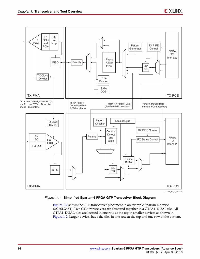
Figure 1-1 illustrates a block view of the Spartan-6 FPGA GTP transceiver. The functional blocks of the receiver and transmitter including their use models are described in their respective chapters of this user guide.
14 www.xilinx.com Spartan-6 FPGA GTP Transceivers (Advance Spec)UG386 (v2.2) April 30, 2010
Chapter 1: Transceiver and Tool Overview
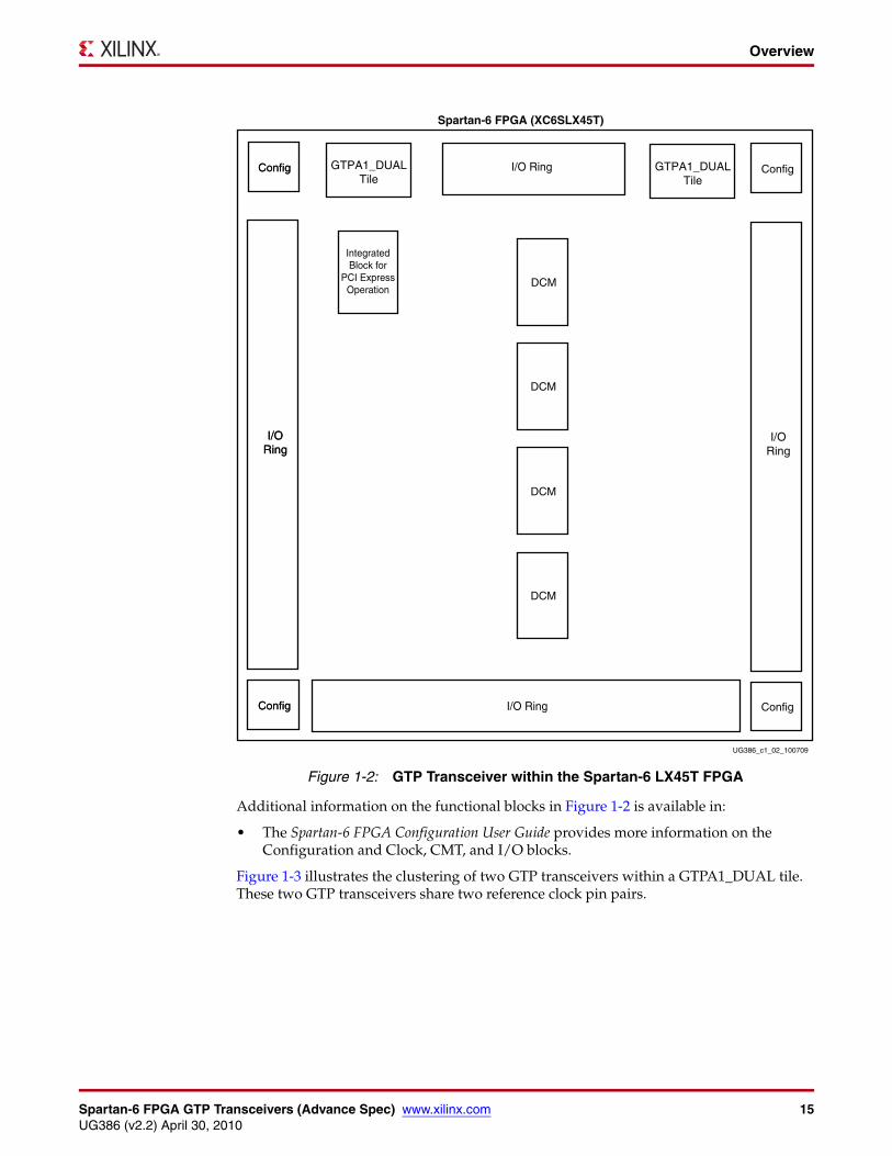
Figure 1-2 shows the GTP transceiver placement in an example Spartan-6 device (XC6SLX45T). Two GTP transceivers are clustered together in a GTPA1_DUAL tile. All GTPA1_DUAL tiles are located in one row at the top in smaller devices as shown in Figure 1-2. Larger devices have the tiles in one row at the top and one row at the bottom.
X-Ref Target - Figure 1-1
Figure 1-1: Simplified Spartan-6 FPGA GTP Transceiver Block Diagram
TX-PMA TX-PCS
FPGATX
Interface
UG386_c1_01_100709
TX PIPEControl
PhaseAdjustFIFO
PCIeBeacon
From RX Parallel Data(Far-End PMA Loopback)
To RX ParallelData (Near-End PCS Loopback)
From RX Parallel Data(Far-End PCS Loopback)
PISO
TXPre-emp
TX Clock Divider
TXOOBandPCIe
TXDriver
Polarity
Polarity
SATAOOB
8B/10B
PatternGenerator
RX-PMA RX-PCS
FPGARX
Interface
Loss of Sync
RX PIPE Control
RX Status Control
SIPO
RX Clock Divider
RXEQ
RX OOB
RXCDR
ElasticBuffer
PatternChecker
CommaDetect
andAlign
10B/8B
Clock from GTPA1_DUAL PLL(s):one PLL per GTPA1_DUAL tileor one PLL per lane
Spartan-6 FPGA GTP Transceivers (Advance Spec) www.xilinx.com 15UG386 (v2.2) April 30, 2010
Overview
Additional information on the functional blocks in Figure 1-2 is available in:
• The Spartan-6 FPGA Configuration User Guide provides more information on the Configuration and Clock, CMT, and I/O blocks.
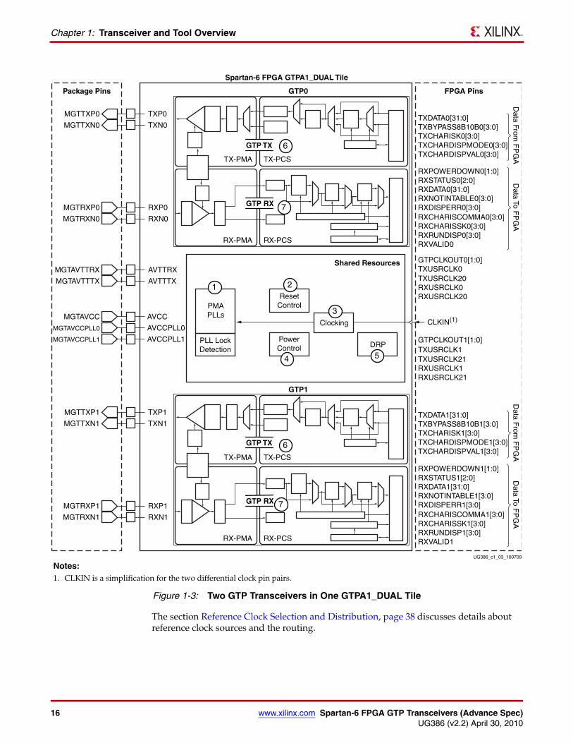
Figure 1-3 illustrates the clustering of two GTP transceivers within a GTPA1_DUAL tile. These two GTP transceivers share two reference clock pin pairs.
X-Ref Target - Figure 1-2
Figure 1-2: GTP Transceiver within the Spartan-6 LX45T FPGA
Config
Config
I/ORing
Spartan-6 FPGA (XC6SLX45T)
UG386_c1_02_100709
IntegratedBlock for
PCI ExpressOperation
GTPA1_DUALTile
GTPA1_DUALTile
DCM
DCM
DCM
DCM
Config
Config
I/ORing
Config
Config
I/ORing
I/O Ring
I/O Ring
16 www.xilinx.com Spartan-6 FPGA GTP Transceivers (Advance Spec)UG386 (v2.2) April 30, 2010
Chapter 1: Transceiver and Tool Overview
The section Reference Clock Selection and Distribution, page 38 discusses details about reference clock sources and the routing.
X-Ref Target - Figure 1-3
Figure 1-3: Two GTP Transceivers in One GTPA1_DUAL Tile
RX-PMA RX-PCS
GTP1
GTP0
Spartan-6 FPGA GTPA1_DUAL Tile
FPGA PinsPackage Pins
Shared Resources
TX-PMA TX-PCS
UG386_c1_03_100709
RX-PMA RX-PCS
TX-PMA TX-PCS
PMAPLLs
PLL LockDetection
ResetControl
TXDATA0[31:0]TXBYPASS8B10B0[3:0]TXCHARISK0[3:0]TXCHARDISPMODE0[3:0]TXCHARDISPVAL0[3:0]
TXDATA1[31:0]TXBYPASS8B10B1[3:0]TXCHARISK1[3:0]TXCHARDISPMODE1[3:0]TXCHARDISPVAL1[3:0]
RXPOWERDOWN0[1:0]RXSTATUS0[2:0]RXDATA0[31:0]RXNOTINTABLE0[3:0]RXDISPERR0[3:0]RXCHARISCOMMA0[3:0]RXCHARISSK0[3:0]RXRUNDISP0[3:0]RXVALID0
RXPOWERDOWN1[1:0]RXSTATUS1[2:0]RXDATA1[31:0]RXNOTINTABLE1[3:0]RXDISPERR1[3:0]RXCHARISCOMMA1[3:0]RXCHARISSK1[3:0]RXRUNDISP1[3:0]
GTPCLKOUT0[1:0]
GTPCLKOUT1[1:0]
TXUSRCLK0TXUSRCLK20RXUSRCLK0RXUSRCLK20
CLKIN(1)
Data From
FP
GA
TXUSRCLK1TXUSRCLK21RXUSRCLK1RXUSRCLK21
Clocking
PowerControl DRP
TXP0MGTTXP0
TXN0MGTTXN0
RXP0MGTRXP0
RXN0MGTRXN0
TXP1MGTTXP1
TXN1MGTTXN1
RXP1MGTRXP1
RXN1MGTRXN1
AVTTRX
AVTTTX
AVCC
AVCCPLL0
Data From
FP
GA
Data To F
PG
A
MGTAVCC
MGTAVCCPLL0
AVCCPLL1MGTAVCCPLL1
MGTAVTTRX
MGTAVTTTX
Data To F
PG
A
RXVALID1
GTP TX
GTP RX
GTP TX
GTP RX
7
6
6
7
4 5
3
21
Notes: 1. CLKIN is a simplification for the two differential clock pin pairs.
Spartan-6 FPGA GTP Transceivers (Advance Spec) www.xilinx.com 17UG386 (v2.2) April 30, 2010
Port and Attribute Summary
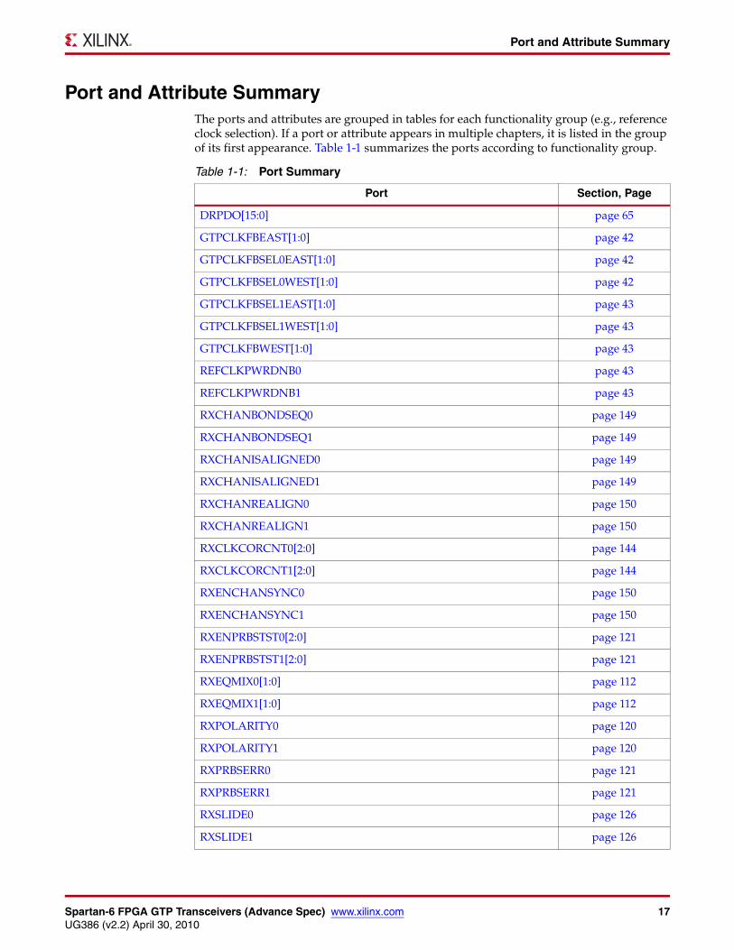
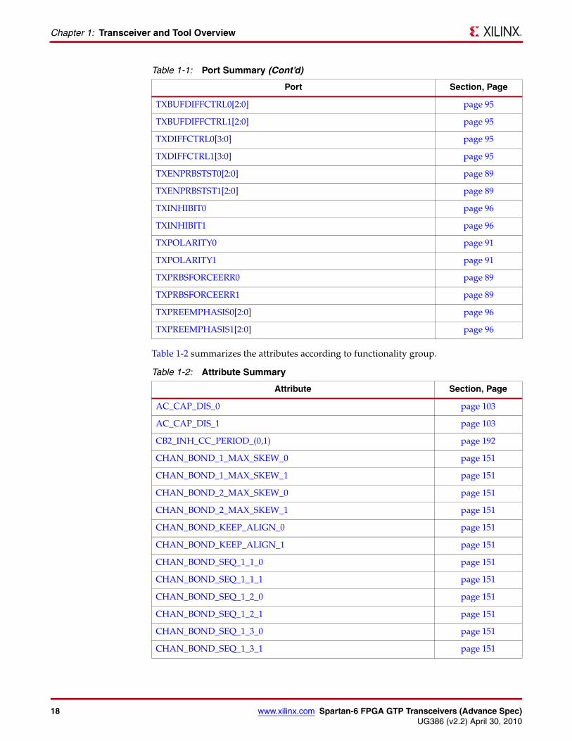
Port and Attribute SummaryThe ports and attributes are grouped in tables for each functionality group (e.g., reference clock selection). If a port or attribute appears in multiple chapters, it is listed in the group of its first appearance. Table 1-1 summarizes the ports according to functionality group.
Table 1-1: Port Summary
Port Section, Page
DRPDO[15:0] page 65
GTPCLKFBEAST[1:0] page 42
GTPCLKFBSEL0EAST[1:0] page 42
GTPCLKFBSEL0WEST[1:0] page 42
GTPCLKFBSEL1EAST[1:0] page 43
GTPCLKFBSEL1WEST[1:0] page 43
GTPCLKFBWEST[1:0] page 43
REFCLKPWRDNB0 page 43
REFCLKPWRDNB1 page 43
RXCHANBONDSEQ0 page 149
RXCHANBONDSEQ1 page 149
RXCHANISALIGNED0 page 149
RXCHANISALIGNED1 page 149
RXCHANREALIGN0 page 150
RXCHANREALIGN1 page 150
RXCLKCORCNT0[2:0] page 144
RXCLKCORCNT1[2:0] page 144
RXENCHANSYNC0 page 150
RXENCHANSYNC1 page 150
RXENPRBSTST0[2:0] page 121
RXENPRBSTST1[2:0] page 121
RXEQMIX0[1:0] page 112
RXEQMIX1[1:0] page 112
RXPOLARITY0 page 120
RXPOLARITY1 page 120
RXPRBSERR0 page 121
RXPRBSERR1 page 121
RXSLIDE0 page 126
RXSLIDE1 page 126
18 www.xilinx.com Spartan-6 FPGA GTP Transceivers (Advance Spec)UG386 (v2.2) April 30, 2010
Chapter 1: Transceiver and Tool Overview
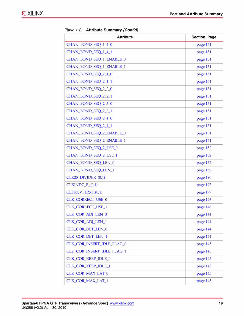
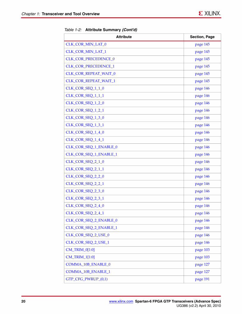
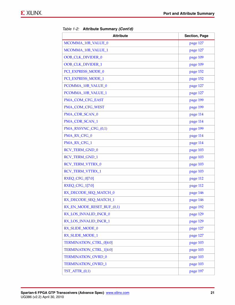
Table 1-2 summarizes the attributes according to functionality group.
TXBUFDIFFCTRL0[2:0] page 95
TXBUFDIFFCTRL1[2:0] page 95
TXDIFFCTRL0[3:0] page 95
TXDIFFCTRL1[3:0] page 95
TXENPRBSTST0[2:0] page 89
TXENPRBSTST1[2:0] page 89
TXINHIBIT0 page 96
TXINHIBIT1 page 96
TXPOLARITY0 page 91
TXPOLARITY1 page 91
TXPRBSFORCEERR0 page 89
TXPRBSFORCEERR1 page 89
TXPREEMPHASIS0[2:0] page 96
TXPREEMPHASIS1[2:0] page 96
Table 1-2: Attribute Summary
Attribute Section, Page
AC_CAP_DIS_0 page 103
AC_CAP_DIS_1 page 103
CB2_INH_CC_PERIOD_(0,1) page 192
CHAN_BOND_1_MAX_SKEW_0 page 151
CHAN_BOND_1_MAX_SKEW_1 page 151
CHAN_BOND_2_MAX_SKEW_0 page 151
CHAN_BOND_2_MAX_SKEW_1 page 151
CHAN_BOND_KEEP_ALIGN_0 page 151
CHAN_BOND_KEEP_ALIGN_1 page 151
CHAN_BOND_SEQ_1_1_0 page 151
CHAN_BOND_SEQ_1_1_1 page 151
CHAN_BOND_SEQ_1_2_0 page 151
CHAN_BOND_SEQ_1_2_1 page 151
CHAN_BOND_SEQ_1_3_0 page 151
CHAN_BOND_SEQ_1_3_1 page 151
Table 1-1: Port Summary (Cont’d)
Port Section, Page
Spartan-6 FPGA GTP Transceivers (Advance Spec) www.xilinx.com 19UG386 (v2.2) April 30, 2010
Port and Attribute Summary
CHAN_BOND_SEQ_1_4_0 page 151
CHAN_BOND_SEQ_1_4_1 page 151
CHAN_BOND_SEQ_1_ENABLE_0 page 151
CHAN_BOND_SEQ_1_ENABLE_1 page 151
CHAN_BOND_SEQ_2_1_0 page 151
CHAN_BOND_SEQ_2_1_1 page 151
CHAN_BOND_SEQ_2_2_0 page 151
CHAN_BOND_SEQ_2_2_1 page 151
CHAN_BOND_SEQ_2_3_0 page 151
CHAN_BOND_SEQ_2_3_1 page 151
CHAN_BOND_SEQ_2_4_0 page 151
CHAN_BOND_SEQ_2_4_1 page 151
CHAN_BOND_SEQ_2_ENABLE_0 page 151
CHAN_BOND_SEQ_2_ENABLE_1 page 151
CHAN_BOND_SEQ_2_USE_0 page 152
CHAN_BOND_SEQ_2_USE_1 page 152
CHAN_BOND_SEQ_LEN_0 page 152
CHAN_BOND_SEQ_LEN_1 page 152
CLK25_DIVIDER_(0,1) page 190
CLKINDC_B_(0,1) page 197
CLKRCV_TRST_(0,1) page 197
CLK_CORRECT_USE_0 page 146
CLK_CORRECT_USE_1 page 146
CLK_COR_ADJ_LEN_0 page 144
CLK_COR_ADJ_LEN_1 page 144
CLK_COR_DET_LEN_0 page 144
CLK_COR_DET_LEN_1 page 144
CLK_COR_INSERT_IDLE_FLAG_0 page 145
CLK_COR_INSERT_IDLE_FLAG_1 page 145
CLK_COR_KEEP_IDLE_0 page 145
CLK_COR_KEEP_IDLE_1 page 145
CLK_COR_MAX_LAT_0 page 145
CLK_COR_MAX_LAT_1 page 145
Table 1-2: Attribute Summary (Cont’d)
Attribute Section, Page
20 www.xilinx.com Spartan-6 FPGA GTP Transceivers (Advance Spec)UG386 (v2.2) April 30, 2010
Chapter 1: Transceiver and Tool Overview
CLK_COR_MIN_LAT_0 page 145
CLK_COR_MIN_LAT_1 page 145
CLK_COR_PRECEDENCE_0 page 145
CLK_COR_PRECEDENCE_1 page 145
CLK_COR_REPEAT_WAIT_0 page 145
CLK_COR_REPEAT_WAIT_1 page 145
CLK_COR_SEQ_1_1_0 page 146
CLK_COR_SEQ_1_1_1 page 146
CLK_COR_SEQ_1_2_0 page 146
CLK_COR_SEQ_1_2_1 page 146
CLK_COR_SEQ_1_3_0 page 146
CLK_COR_SEQ_1_3_1 page 146
CLK_COR_SEQ_1_4_0 page 146
CLK_COR_SEQ_1_4_1 page 146
CLK_COR_SEQ_1_ENABLE_0 page 146
CLK_COR_SEQ_1_ENABLE_1 page 146
CLK_COR_SEQ_2_1_0 page 146
CLK_COR_SEQ_2_1_1 page 146
CLK_COR_SEQ_2_2_0 page 146
CLK_COR_SEQ_2_2_1 page 146
CLK_COR_SEQ_2_3_0 page 146
CLK_COR_SEQ_2_3_1 page 146
CLK_COR_SEQ_2_4_0 page 146
CLK_COR_SEQ_2_4_1 page 146
CLK_COR_SEQ_2_ENABLE_0 page 146
CLK_COR_SEQ_2_ENABLE_1 page 146
CLK_COR_SEQ_2_USE_0 page 146
CLK_COR_SEQ_2_USE_1 page 146
CM_TRIM_0[1:0] page 103
CM_TRIM_1[1:0] page 103
COMMA_10B_ENABLE_0 page 127
COMMA_10B_ENABLE_1 page 127
GTP_CFG_PWRUP_(0,1) page 191
Table 1-2: Attribute Summary (Cont’d)
Attribute Section, Page
Spartan-6 FPGA GTP Transceivers (Advance Spec) www.xilinx.com 21UG386 (v2.2) April 30, 2010
Port and Attribute Summary
MCOMMA_10B_VALUE_0 page 127
MCOMMA_10B_VALUE_1 page 127
OOB_CLK_DIVIDER_0 page 109
OOB_CLK_DIVIDER_1 page 109
PCI_EXPRESS_MODE_0 page 152
PCI_EXPRESS_MODE_1 page 152
PCOMMA_10B_VALUE_0 page 127
PCOMMA_10B_VALUE_1 page 127
PMA_COM_CFG_EAST page 199
PMA_COM_CFG_WEST page 199
PMA_CDR_SCAN_0 page 114
PMA_CDR_SCAN_1 page 114
PMA_RXSYNC_CFG_(0,1) page 199
PMA_RX_CFG_0 page 114
PMA_RX_CFG_1 page 114
RCV_TERM_GND_0 page 103
RCV_TERM_GND_1 page 103
RCV_TERM_VTTRX_0 page 103
RCV_TERM_VTTRX_1 page 103
RXEQ_CFG_0[7:0] page 112
RXEQ_CFG_1[7:0] page 112
RX_DECODE_SEQ_MATCH_0 page 146
RX_DECODE_SEQ_MATCH_1 page 146
RX_EN_MODE_RESET_BUF_(0,1) page 192
RX_LOS_INVALID_INCR_0 page 129
RX_LOS_INVALID_INCR_1 page 129
RX_SLIDE_MODE_0 page 127
RX_SLIDE_MODE_1 page 127
TERMINATION_CTRL_0[4:0] page 103
TERMINATION_CTRL_1[4:0] page 103
TERMINATION_OVRD_0 page 103
TERMINATION_OVRD_1 page 103
TST_ATTR_(0,1) page 197
Table 1-2: Attribute Summary (Cont’d)
Attribute Section, Page
22 www.xilinx.com Spartan-6 FPGA GTP Transceivers (Advance Spec)UG386 (v2.2) April 30, 2010
Chapter 1: Transceiver and Tool Overview
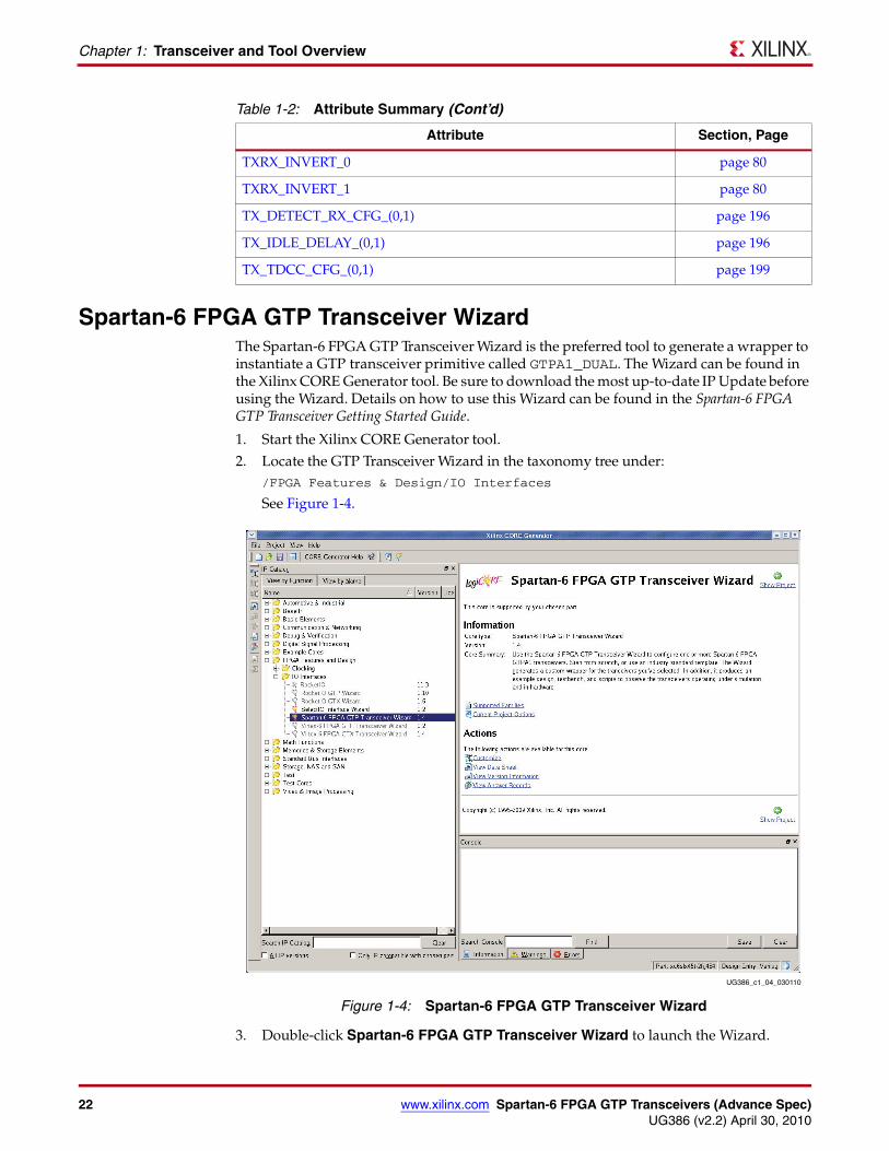
Spartan-6 FPGA GTP Transceiver WizardThe Spartan-6 FPGA GTP Transceiver Wizard is the preferred tool to generate a wrapper to instantiate a GTP transceiver primitive called GTPA1_DUAL. The Wizard can be found in the Xilinx CORE Generator tool. Be sure to download the most up-to-date IP Update before using the Wizard. Details on how to use this Wizard can be found in the Spartan-6 FPGA GTP Transceiver Getting Started Guide.
1. Start the Xilinx CORE Generator tool.2. Locate the GTP Transceiver Wizard in the taxonomy tree under:
/FPGA Features & Design/IO Interfaces
See Figure 1-4.
3. Double-click Spartan-6 FPGA GTP Transceiver Wizard to launch the Wizard.
TXRX_INVERT_0 page 80
TXRX_INVERT_1 page 80
TX_DETECT_RX_CFG_(0,1) page 196
TX_IDLE_DELAY_(0,1) page 196
TX_TDCC_CFG_(0,1) page 199
Table 1-2: Attribute Summary (Cont’d)
Attribute Section, Page
X-Ref Target - Figure 1-4
Figure 1-4: Spartan-6 FPGA GTP Transceiver Wizard
UG386_c1_04_030110
Spartan-6 FPGA GTP Transceivers (Advance Spec) www.xilinx.com 23UG386 (v2.2) April 30, 2010
Simulation
Simulation
Functional DescriptionSimulations using GTP transceivers have specific prerequisites that the simulation environment and the test bench must fulfill.
The Synthesis and Simulation Design Guide [Ref 2] explains how to set up the simulation environment for supported simulators depending on the used Hardware Description Language (HDL). This design guide can be downloaded from the Xilinx website.
The prerequisites for simulating a design with GTP transceivers are:
• Simulator with support for SecureIP models, which are encrypted versions of the Verilog HDL used for implementation of the modeled block.
SecureIP is a new IP encryption methodology. To support SecureIP models, a Verilog LRM - IEEE Std 1364-2005 encryption compliant simulator is required.
• Mixed-language simulator for VHDL simulation.
SecureIP models use a Verilog standard. To use them in a VHDL design, a mixed-language simulator is required. The simulator must be capable of simulating VHDL and Verilog simultaneously.
• Installed GTPA1_DUAL SecureIP model.
• Correct setup of the simulator for SecureIP use (initialization file, environment variable(s)).
• Running COMPXLIB (which compiles the simulation libraries (e.g. UNISIM, SIMPRIMS, etc.) in the correct order.
• Correct simulator resolution (Verilog)
• The user guide of the simulator and the Synthesis and Simulation Design Guide provide a detailed list of settings for SecureIP support.
Simulation-only Ports and AttributesThe GTPA1_DUAL primitive has attributes intended only for simulation. Table 1-3 lists the simulation-only attributes of the GTPA1_DUAL primitive. The names of these attributes start with SIM_.
24 www.xilinx.com Spartan-6 FPGA GTP Transceivers (Advance Spec)UG386 (v2.2) April 30, 2010
Chapter 1: Transceiver and Tool Overview
Table 1-3: GTPA1_DUAL Simulation-Only Attributes
Attribute Type Description
SIM_GTPRESET_SPEEDUP Integer This attribute shortens the time it takes to finish the GTPRESET sequence and lock the PMA PLL in each GTP transceiver during simulation.
0: The GTPRESET sequence is simulated with its original duration (standard initialization is approximately 160 µs).
1: Shorten the GTPRESET cycle time (fast initialization is approximately 300 ns).
SIM_RECEIVER_DETECT_PASS Boolean This attribute simulates the TXDETECTRX feature in the GTP transceiver.
TRUE: Simulates an RX connection to the TX serial ports. TXDETECTRX initiates receiver detection, and RXSTATUS[2:0] = 011 reports that an RX port is detected.
FALSE (default): Simulates a disconnected TX port. TXDETECTRX initiates receiver detection, and RXSTATUS[2:0] = 000 reports that an RX port is not detected.
SIM_REFCLK0_SOURCE 3-Bit Binary This attribute selects the reference clock source used to drive the GTP0 transceiver’s PMA PLL in simulation for designs where the GTP0 transceiver’s PMA PLL is always driven by the same reference clock source. REFSELDYPLL0 must be set to 000 for this attribute to select the reference clock source. For multi-rate designs that require the reference clock source to be changed on the fly, the REFSELDYPLL0 port is used to dynamically select the source instead.
000: Selects the CLK00 port as the source
001: Selects the GCLK00 port as the source
010: Selects the PLLCLK00 port as the source
011: Selects the CLKINEAST0 port as the source
100: Selects the CLK10 port as the source
101: Selects the GCLK10 port as the source
110: Selects the PLLCLK10 port as the source
111: Selects the CLKINWEST0 port as the source
Spartan-6 FPGA GTP Transceivers (Advance Spec) www.xilinx.com 25UG386 (v2.2) April 30, 2010
Simulation
There are no simulation-only ports.
SIM_GTPRESET_SPEEDUP
The SIM_GTPRESET_SPEEDUP attribute can be used to shorten the simulated lock time of the PMA PLL in each GTP transceiver.
If TXOUTCLK or RXRECCLK is used to generate clocks in the design, these clocks occasionally flatline while the GTP transceiver is locking. If a PLL or a digital clock manager (DCM) is used to divide TXOUTCLK or RXRECCLK, the final output clock is not ready until both the GTP transceiver and the PLL or DCM have locked. Equation 1-1 provides an estimate of the time required before a stable source from TXOUTCLK or RXRECCLK is available in simulation, including the time required for any PLLs or DCMs used.
Equation 1-1
If either the PLL or the DCM is not used, the respective term can be removed from the lock time equation.
SIM_RECEIVER_DETECT_PASS
The GTP transceiver includes a TXDETECTRX feature that allows the transmitter to detect whether its serial ports are currently connected to a receiver by measuring rise time on the TXP/TXN differential pin pair (see TX Receiver Detect Support for PCI Express Designs, page 97).
The GTPA1_DUAL SecureIP model includes an attribute for simulating TXDETECTRX called SIM_RECEIVER_DETECT_PASS. This attribute allows TXDETECTRX to be
SIM_REFCLK1_SOURCE 3-Bit Binary This attribute selects the reference clock source used to drive the GTP1 transceiver’s PMA PLL in simulation for designs where the GTP1 transceiver’s PMA PLL is always driven by the same reference clock source. REFSELDYPLL1 must be set to 000 for this attribute to select the reference clock source. For multi-rate designs that require the reference clock source to be changed on the fly, the REFSELDYPLL1 port is used to dynamically select the source instead.
000: Selects the CLK01 port as the source
001: Selects the GCLK01 port as the source
010: Selects the PLLCLK01 port as the source
011: Selects the CLKINEAST1 port as the source
100: Selects the CLK11 port as the source
101: Selects the GCLK11 port as the source
110: Selects the PLLCLK11 port as the source
111: Selects the CLKINWEST1 port as the source
SIM_TX_ELEC_IDLE_LEVEL 1-Bit Binary This attribute sets the value of TXN and TXP during simulation of electrical idle. This attribute can be set to 0, 1, X, or Z. The default for this attribute is X.
SIM_VERSION Real This attribute selects the simulation version to match different steppings of silicon. The default for this attribute is 2.0.
Table 1-3: GTPA1_DUAL Simulation-Only Attributes (Cont’d)
Attribute Type Description
tUSRCLKstable tGTPRESETsequence tlocktimeDCM t+ locktimePLL+≅
26 www.xilinx.com Spartan-6 FPGA GTP Transceivers (Advance Spec)UG386 (v2.2) April 30, 2010
Chapter 1: Transceiver and Tool Overview
simulated for the GTP transceiver without modeling the measurement of rise time on the TXP/TXN differential pin pair.
By default, SIM_RECEIVER_DETECT_PASS is set to FALSE. When FALSE, the attribute models a disconnected receiver and TXDETECTRX operations indicate a receiver is disconnected. To model a connected receiver, SIM_RECEIVER_DETECT_PASS for the transceiver is set to TRUE.
SIM_REFCLK0_SOURCE
The GTPA1_DUAL SecureIP model includes an attribute to select the reference clock source used to drive the GTP0 transceiver’s PMA PLL in simulation called SIM_REFCLK0_SOURCE. This attribute is to be used in designs where the clock input to the GTP0 transceiver’s PMA PLL is always driven by the same reference clock source.
Reference clock sources include the dedicated clock pins of the tile that the transceiver belongs to, the west-running reference clock, the east-running reference clock, and clocks from the FPGA logic. Table 1-3, page 24 shows the possible settings for this attribute.
For multi-rate designs requiring the reference clock source driving the GTP0 transceiver’s PMA PLL to be changed on the fly, the REFSELDYPLL0 port is used to dynamically select the reference clock source instead.
SIM_REFCLK1_SOURCE
The GTPA1_DUAL SecureIP model includes an attribute to select the reference clock source used to drive the GTP1 transceiver’s PMA PLL in simulation called SIM_REFCLK1_SOURCE. This attribute is to be used in designs where the clock input to the GTP1 transceiver’s PMA PLL is always driven by the same reference clock source.
Reference clock sources include the dedicated clock pins of the tile that the transceiver belongs to, the west-running reference clock, the east-running reference clock, and clocks from the FPGA logic. Table 1-3, page 24 shows the possible settings for this attribute.
For multi-rate designs requiring the reference clock source driving the GTP1 transceiver’s PMA PLL to be changed on the fly, the REFSELDYPLL1 port is used to dynamically select the reference clock source instead.
SIM_TX_ELEC_IDLE_LEVEL
The SIM_TX_ELEC_IDLE_LEVEL attribute sets the value of the transceiver’s differential transmitter output pair TXN and TXP during simulation of electrical idle. This attribute can be set to 0, 1, X, or Z. The default for this attribute is X.
SIM_VERSION
The SIM_VERSION attribute selects the simulation version to match different steppings of silicon. The default for this attribute is 2.0.
ImplementationThis section provides the information needed to map Spartan-6 FPGA GTPA1_DUAL tiles instantiated in a design to device resources, including:
• The location of the GTPA1_DUAL tiles on the available device and package combinations
• The pad numbers of external signals associated with each GTPA1_DUAL tile
Spartan-6 FPGA GTP Transceivers (Advance Spec) www.xilinx.com 27UG386 (v2.2) April 30, 2010
Implementation
• How GTPA1_DUAL tiles and clocking resources instantiated in a design are mapped to available locations with a user constraints file (UCF)
It is a common practice to define the location of GTP transceivers early in the design process to ensure correct usage of clock resources and to facilitate signal integrity analysis during board design. The implementation flow facilitates this practice through the use of location constraints in the UCF.
While this section describes how to instantiate GTP clocking components, the details of the different GTPA1_DUAL tile clocking options are discussed in Reference Clock Selection and Distribution, page 38.
The position of GTPA1_DUAL tiles is specified by an XY coordinate system (where X = column, Y = row). In Spartan-6 devices, all GTP transceivers are located in a row along the top side of the die for small devices. Larger devices have one GTP transceiver row at the top and one GTP transceiver row at the bottom.
The transceiver with the coordinates X0Y0 is for a given device/package combination always located at the lowest position of the lowest available bank. If a device has only a top row, the value of the Y coordinate is always 0. If a device has a top row and a bottom row, the value of the Y coordinate of the bottom row is 0, and the value of the Y coordinate for the top row is 1.
There are two ways to create a UCF for designs that utilize GTP transceivers. The preferred method is by using the GTP Transceiver Wizard (see Spartan-6 FPGA GTP Transceiver Wizard, page 22). The Wizard automatically generates UCF templates that configure the transceivers and contain placeholders for GTPA1_DUAL placement information. The UCFs generated by the Wizard can then be edited to customize operating parameters and placement information for the application.
The second approach is to create the UCF by hand. When using this approach, the designer must enter both configuration attributes that control transceiver operation as well as tile location parameters. Care must be taken to ensure that all of the parameters needed to configure the GTP transceiver are correctly entered.
28 www.xilinx.com Spartan-6 FPGA GTP Transceivers (Advance Spec)UG386 (v2.2) April 30, 2010
Chapter 1: Transceiver and Tool Overview
CSG324 Package Placement DiagramsFigure 1-5 lists the GTP transceiver position information for the left side of die for all available devices in the CSG324 package.
Figure 1-6 lists the GTP transceiver position information for the right side of die for all available devices in the CSG324 package.
X-Ref Target - Figure 1-5
Figure 1-5: Placement Diagram for the CSG324 Package (1 of 2)
XC6SLX25T: GTPA1_DUAL_X0Y0XC6SLX45T: GTPA1_DUAL_X0Y0
B6B4
A6A4
C5C7
D5D7
A8B8
C9D9
MGTTXP1_101MGTTXP0_101
MGTTXN1_101MGTTXN0_101
MGTRXN0_101MGTRXN1_101
MGTRXP0_101MGTRXP1_101
MGTREFCLK0N_101MGTREFCLK0P_101
MGTREFCLK1N_101MGTREFCLK1P_101
B7D10
C8
D6A5
E7E5
MGTAVCCPLL0_101MGTAVCCPLL1_101
MGTAVCC_101
MGTAVTTRX_101MGTAVTTTX_101
MGTRREF_101MGTAVTTRCAL_101
UG386_c1_05_100909
Top
X-Ref Target - Figure 1-6
Figure 1-6: Placement Diagram for the CSG324 Package (2 of 2)
UG386_c1_06_100909
XC6SLX25T: Not AvailableXC6SLX45T: GTPA1_DUAL_X1Y0
B14B12
A14A12
C11C13
D11D13
A10B10
E10F10
MGTTXP1_123MGTTXP0_123
MGTTXN1_123MGTTXN0_123
MGTRXN0_123MGTRXN1_123
MGTRXP0_123MGTRXP1_123
MGTREFCLK0N_123MGTREFCLK0P_123
MGTREFCLK1N_123MGTREFCLK1P_123
B11E11
E9
D12A13
MGTAVCCPLL0_123MGTAVCCPLL1_123
MGTAVCC_123
MGTAVTTRX_123MGTAVTTTX_123
Top
Spartan-6 FPGA GTP Transceivers (Advance Spec) www.xilinx.com 29UG386 (v2.2) April 30, 2010
Implementation
CSG484 Package Placement DiagramsFigure 1-7 lists the GTP transceiver position information for the left side of die for all available devices in the CSG484 package.
X-Ref Target - Figure 1-7
Figure 1-7: Placement Diagram for the CSG484 Package (1 of 2)
Bottom UG386_c1_13_031510
B8B6
A8A6
C7C9
D7D9
A10B10
C11D11
Top
XC6SLX45T: GTPA1_DUAL_X0Y0 XC6SLX75T: GTPA1_DUAL_X0Y1 XC6SLX100T: GTPA1_DUAL_X0Y1 XC6SLX150T: GTPA1_DUAL_X0Y1
MGTTXP1_101MGTTXP0_101
MGTTXN1_101MGTTXN0_101
MGTRXN0_101MGTRXN1_101
MGTRXP0_101MGTRXP1_101
MGTREFCLK0N_101MGTREFCLK0P_101
MGTREFCLK1N_101MGTREFCLK1P_101
MGTAVCCPLL0_101MGTAVCCPLL1_101
B9D12
MGTAVCC_101 C10
MGTAVTTRX_101MGTAVTTTX_101
D8A7
MGTRREF_101MGTAVTTRCAL_101
E9E11
XC6SLX45T: Not AvailableXC6SLX75T: GTPA1_DUAL_X0Y0XC6SLX100T: GTPA1_DUAL_X0Y0XC6SLX150T: GTPA1_DUAL_X0Y0
UNBUNB
UNBUNB
UNBUNB
UNBUNB
UNBUNB
UNBUNB
OPAD_X0Y0OPAD_X0Y1
OPAD_X0Y2OPAD_X0Y3
IPAD_X0Y0IPAD_X0Y1
IPAD_X0Y2IPAD_X0Y3
IPAD_X0Y4IPAD_X0Y5
IPAD_X0Y6IPAD_X0Y7
30 www.xilinx.com Spartan-6 FPGA GTP Transceivers (Advance Spec)UG386 (v2.2) April 30, 2010
Chapter 1: Transceiver and Tool Overview
Figure 1-8 lists the GTP transceiver position information for the right side of die for all available devices in the CSG484 package.
X-Ref Target - Figure 1-8
Figure 1-8: Placement Diagram for the CSG484 Package (2 of 2)
Bottom UG386_c1_14_031510
Top
XC6SLX45T: GTPA1_DUAL_X1Y0 XC6SLX75T: GTPA1_DUAL_X1Y1 XC6SLX100T: GTPA1_DUAL_X1Y1 XC6SLX150T: GTPA1_DUAL_X1Y1
B16B14
A16A14
C13C15
D13D15
A12B12
E14F14
MGTTXP1_123MGTTXP0_123
MGTTXN1_123MGTTXN0_123
MGTRXN0_123MGTRXN1_123
MGTRXP0_123MGTRXP1_123
MGTREFCLK0N_123MGTREFCLK0P_123
MGTREFCLK1N_123MGTREFCLK1P_123
B13E13
MGTAVCCPLL0_123MGTAVCCPLL1_123
E15 MGTAVCC_123
D14A15
MGTAVTTRX_123MGTAVTTTX_123
XC6SLX45T: Not AvailableXC6SLX75T: GTPA1_DUAL_X1Y0XC6SLX100T: GTPA1_DUAL_X1Y0XC6SLX150T: GTPA1_DUAL_X1Y0
UNBUNB
UNBUNB
UNBUNB
UNBUNB
UNBUNB
UNBUNB
OPAD_X1Y0OPAD_X1Y1
OPAD_X1Y2OPAD_X1Y3
IPAD_X1Y0IPAD_X1Y1
IPAD_X1Y2IPAD_X1Y3
IPAD_X1Y4IPAD_X1Y5
IPAD_X1Y6IPAD_X1Y7
Spartan-6 FPGA GTP Transceivers (Advance Spec) www.xilinx.com 31UG386 (v2.2) April 30, 2010
Implementation
FG(G)484 Package Placement DiagramsFigure 1-9 lists the GTP transceiver position information for the left side of die for all available devices in the FG(G)484 package.
X-Ref Target - Figure 1-9
Figure 1-9: Placement Diagram for the FG(G)484 Package (1 of 2)
Bottom UG386_c1_07_100909
B8B6
A8A6
C7C9
D7D9
B10A10
D11C11
Top
XC6SLX25T: GTPA1_DUAL_X0Y0 XC6SLX45T: GTPA1_DUAL_X0Y0 XC6SLX75T: GTPA1_DUAL_X0Y1 XC6SLX100T: GTPA1_DUAL_X0Y1 XC6SLX150T: GTPA1_DUAL_X0Y1
MGTTXP1_101MGTTXP0_101
MGTTXN1_101MGTTXN0_101
MGTRXN0_101MGTRXN1_101
MGTRXP0_101MGTRXP1_101
MGTREFCLK0N_101MGTREFCLK0P_101
MGTREFCLK1N_101MGTREFCLK1P_101
MGTAVCCPLL0_101MGTAVCCPLL1_101
B9D12
MGTAVCC_101 C10
MGTAVTTRX_101MGTAVTTTX_101
D8A7
MGTRREF_101MGTAVTTRCAL_101
E9E8
XC6SLX25T: Not AvailableXC6SLX45T: Not AvailableXC6SLX75T: GTPA1_DUAL_X0Y0XC6SLX100T: GTPA1_DUAL_X0Y0XC6SLX150T: GTPA1_DUAL_X0Y0
UNBUNB
UNBUNB
UNBUNB
UNBUNB
UNBUNB
UNBUNB
OPAD_X0Y0OPAD_X0Y1
OPAD_X0Y2OPAD_X0Y3
IPAD_X0Y0IPAD_X0Y1
IPAD_X0Y2IPAD_X0Y3
IPAD_X0Y4IPAD_X0Y5
IPAD_X0Y6IPAD_X0Y7
32 www.xilinx.com Spartan-6 FPGA GTP Transceivers (Advance Spec)UG386 (v2.2) April 30, 2010
Chapter 1: Transceiver and Tool Overview
Figure 1-10 lists the GTP transceiver position information for the right side of die for all available devices in the FG(G)484 package.
X-Ref Target - Figure 1-10
Figure 1-10: Placement Diagram for the FG(G)484 Package (2 of 2)
Bottom UG386_c1_08_100909
Top
XC6SLX25T: Not AvailableXC6SLX45T: GTPA1_DUAL_X1Y0 XC6SLX75T: GTPA1_DUAL_X1Y1 XC6SLX100T: GTPA1_DUAL_X1Y1 XC6SLX150T: GTPA1_DUAL_X1Y1
B16B14
A16A14
C13C15
D13D15
B12A12
F12E12
MGTTXP1_123MGTTXP0_123
MGTTXN1_123MGTTXN0_123
MGTRXN0_123MGTRXN1_123
MGTRXP0_123MGTRXP1_123
MGTREFCLK0N_123MGTREFCLK0P_123
MGTREFCLK1N_123MGTREFCLK1P_123
B13E13
MGTAVCCPLL0_123MGTAVCCPLL1_123
E10 MGTAVCC_123
D14A15
MGTAVTTRX_123MGTAVTTTX_123
XC6SLX25T: Not AvailableXC6SLX45T: Not AvailableXC6SLX75T: GTPA1_DUAL_X1Y0XC6SLX100T: GTPA1_DUAL_X1Y0XC6SLX150T: GTPA1_DUAL_X1Y0
UNBUNB
UNBUNB
UNBUNB
UNBUNB
UNBUNB
UNBUNB
OPAD_X1Y0OPAD_X1Y1
OPAD_X1Y2OPAD_X1Y3
IPAD_X1Y0IPAD_X1Y1
IPAD_X1Y2IPAD_X1Y3
IPAD_X1Y4IPAD_X1Y5
IPAD_X1Y6IPAD_X1Y7
Spartan-6 FPGA GTP Transceivers (Advance Spec) www.xilinx.com 33UG386 (v2.2) April 30, 2010
Implementation
FG(G)676 Package Placement DiagramsFigure 1-11 lists the GTP transceiver position information for the left side of die for all available devices in the FG(G)676 package.
X-Ref Target - Figure 1-11
Figure 1-11: Placement Diagram for the FG(G)676 Package (1 of 2)
Top
Bottom UG386_c1_09_100909
MGTAVCCPLL0_101MGTAVCCPLL1_101
B11C12
MGTTXP1_101MGTTXP0_101
B8B6
MGTAVCC_101 C10 MGTTXN1_101MGTTXN0_101
A8A6
MGTAVTTRX_101MGTAVTTTX_101
D8A7
MGTRXN0_101MGTRXN1_101
C7C9
MGTRREF_101MGTAVTTRCAL_101
E9E11
MGTRXP0_101MGTRXP1_101
D7D9
MGTREFCLK0N_101MGTREFCLK0P_101
A10B10
MGTREFCLK1N_101MGTREFCLK1P_101
C11D11
XC6SLX75T: GTPA1_DUAL_X0Y1XC6SLX100T: GTPA1_DUAL_X0Y1XC6SLX150T: GTPA1_DUAL_X0Y1
MGTAVCCPLL0_245MGTAVCCPLL1_245
AE12AD13
MGTTXP1_245MGTTXP0_245
AE9AE7
MGTAVCC_245 AD11 MGTTXN1_245MGTTXN0_245
AF9AF7
MGTAVTTRX_245MGTAVTTTX_245
AC9AF8
MGTRXN0_245MGTRXN1_245
AD8AD10
MGTRREF_245MGTAVTTRCAL_245
AB10AB12
MGTRXP0_245MGTRXP1_245
AC8AC10
MGTREFCLK0N_245MGTREFCLK0P_245
AF11AE11
MGTREFCLK1N_245MGTREFCLK1P_245
AD12AC12
XC6SLX75T: GTPA1_DUAL_X0Y0XC6SLX100T: GTPA1_DUAL_X0Y0XC6SLX150T: GTPA1_DUAL_X0Y0
34 www.xilinx.com Spartan-6 FPGA GTP Transceivers (Advance Spec)UG386 (v2.2) April 30, 2010
Chapter 1: Transceiver and Tool Overview
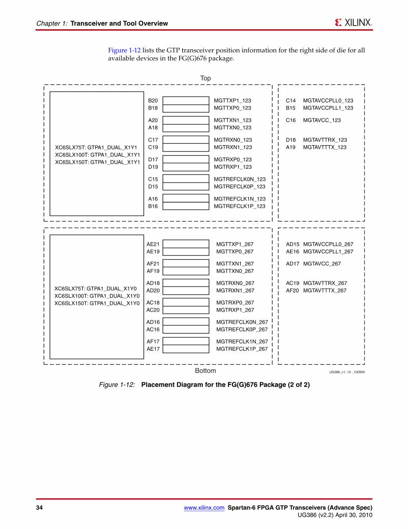
Figure 1-12 lists the GTP transceiver position information for the right side of die for all available devices in the FG(G)676 package.
X-Ref Target - Figure 1-12
Figure 1-12: Placement Diagram for the FG(G)676 Package (2 of 2)
Top
Bottom UG386_c1_10 _100909
XC6SLX75T: GTPA1_DUAL_X1Y1XC6SLX100T: GTPA1_DUAL_X1Y1XC6SLX150T: GTPA1_DUAL_X1Y1
B20B18
A20A18
C17C19
D17D19
C15D15
A16B16
MGTTXP1_123MGTTXP0_123
MGTTXN1_123MGTTXN0_123
MGTRXN0_123MGTRXN1_123
MGTRXP0_123MGTRXP1_123
MGTREFCLK0N_123MGTREFCLK0P_123
MGTREFCLK1N_123MGTREFCLK1P_123
C14B15
MGTAVCCPLL0_123MGTAVCCPLL1_123
C16 MGTAVCC_123
D18A19
MGTAVTTRX_123MGTAVTTTX_123
XC6SLX75T: GTPA1_DUAL_X1Y0XC6SLX100T: GTPA1_DUAL_X1Y0XC6SLX150T: GTPA1_DUAL_X1Y0
AE21AE19
AF21AF19
AD18AD20
AC18AC20
AD16AC16
AF17AE17
MGTTXP1_267MGTTXP0_267
MGTTXN1_267MGTTXN0_267
MGTRXN0_267MGTRXN1_267
MGTRXP0_267MGTRXP1_267
MGTREFCLK0N_267MGTREFCLK0P_267
MGTREFCLK1N_267MGTREFCLK1P_267
AD15AE16
MGTAVCCPLL0_267MGTAVCCPLL1_267
AD17 MGTAVCC_267
AC19AF20
MGTAVTTRX_267MGTAVTTTX_267
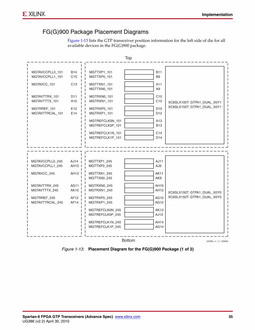
Spartan-6 FPGA GTP Transceivers (Advance Spec) www.xilinx.com 35UG386 (v2.2) April 30, 2010
Implementation
FG(G)900 Package Placement DiagramsFigure 1-13 lists the GTP transceiver position information for the left side of die for all available devices in the FG(G)900 package.
X-Ref Target - Figure 1-13
Figure 1-13: Placement Diagram for the FG(G)900 Package (1 of 2)
Top
Bottom UG386_c1_11_100909
XC6SLX100T: GTPA1_DUAL_X0Y1XC6SLX150T: GTPA1_DUAL_X0Y1
B11B9
A11A9
C10C12
D10D12
A13B13
C14D14
MGTTXP1_101MGTTXP0_101
MGTTXN1_101MGTTXN0_101
MGTRXN0_101MGTRXN1_101
MGTRXP0_101MGTRXP1_101
MGTREFCLK0N_101MGTREFCLK0P_101
MGTREFCLK1N_101MGTREFCLK1P_101
MGTAVCCPLL0_101MGTAVCCPLL1_101
B14C15
MGTAVCC_101 C13
MGTAVTTRX_101MGTAVTTTX_101
D11A10
MGTRREF_101MGTAVTTRCAL_101
E12E14
XC6SLX100T: GTPA1_DUAL_X0Y0XC6SLX150T: GTPA1_DUAL_X0Y0
AJ11AJ9
AK11AK9
AH10AH12
AG10AG12
AK13AJ13
AH14AG14
MGTTXP1_245MGTTXP0_245
MGTTXN1_245MGTTXN0_245
MGTRXN0_245MGTRXN1_245
MGTRXP0_245MGTRXP1_245
MGTREFCLK0N_245MGTREFCLK0P_245
MGTREFCLK1N_245MGTREFCLK1P_245
MGTAVCCPLL0_245MGTAVCCPLL1_245
AJ14AH15
MGTAVCC_245 AH13
MGTAVTTRX_245MGTAVTTTX_245
AG11AK10
MGTRREF_245MGTAVTTRCAL_245
AF12AF14
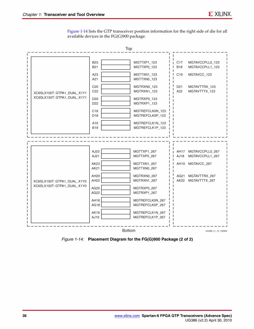
36 www.xilinx.com Spartan-6 FPGA GTP Transceivers (Advance Spec)UG386 (v2.2) April 30, 2010
Chapter 1: Transceiver and Tool Overview
Figure 1-14 lists the GTP transceiver position information for the right side of die for all available devices in the FG(G)900 package.
X-Ref Target - Figure 1-14
Figure 1-14: Placement Diagram for the FG(G)900 Package (2 of 2)
B23B21
A23A21
C20C22
D20D22
C18D18
A19B19
MGTTXP1_123MGTTXP0_123
MGTTXN1_123MGTTXN0_123
MGTRXN0_123MGTRXN1_123
MGTRXP0_123MGTRXP1_123
MGTREFCLK0N_123MGTREFCLK0P_123
MGTREFCLK1N_123MGTREFCLK1P_123
UG386_c1_12_100909
XC6SLX100T: GTPA1_DUAL_X1Y1XC6SLX150T: GTPA1_DUAL_X1Y1
C17B18
MGTAVCCPLL0_123MGTAVCCPLL1_123
C19 MGTAVCC_123
D21A22
MGTAVTTRX_123MGTAVTTTX_123
XC6SLX100T: GTPA1_DUAL_X1Y0XC6SLX150T: GTPA1_DUAL_X1Y0
AJ23AJ21
AK23AK21
AH20AH22
AG20AG22
AH18AG18
AK19AJ19
MGTTXP1_267MGTTXP0_267
MGTTXN1_267MGTTXN0_267
MGTRXN0_267MGTRXN1_267
MGTRXP0_267MGTRXP1_267
MGTREFCLK0N_267MGTREFCLK0P_267
MGTREFCLK1N_267MGTREFCLK1P_267
AH17AJ18
MGTAVCCPLL0_267MGTAVCCPLL1_267
AH19 MGTAVCC_267
AG21AK22
MGTAVTTRX_267MGTAVTTTX_267
Top
Bottom
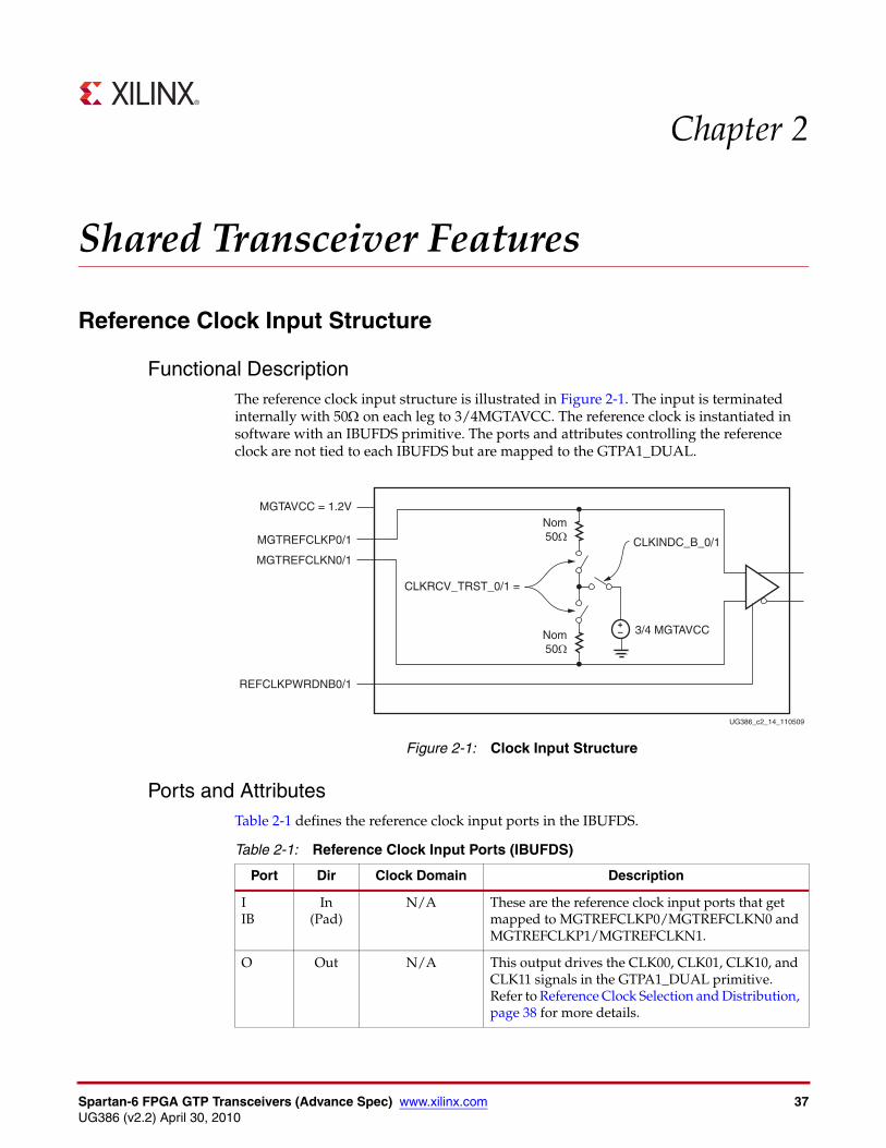
Spartan-6 FPGA GTP Transceivers (Advance Spec) www.xilinx.com 37UG386 (v2.2) April 30, 2010
Chapter 2
Shared Transceiver Features
Reference Clock Input Structure
Functional DescriptionThe reference clock input structure is illustrated in Figure 2-1. The input is terminated internally with 50Ω on each leg to 3/4MGTAVCC. The reference clock is instantiated in software with an IBUFDS primitive. The ports and attributes controlling the reference clock are not tied to each IBUFDS but are mapped to the GTPA1_DUAL.
Ports and AttributesTable 2-1 defines the reference clock input ports in the IBUFDS.
X-Ref Target - Figure 2-1
Figure 2-1: Clock Input Structure
+–
UG386_c2_14_110509
Nom50Ω
CLKRCV_TRST_0/1 =
MGTREFCLKP0/1
MGTREFCLKN0/1
REFCLKPWRDNB0/1
MGTAVCC = 1.2V
CLKINDC_B_0/1
3/4 MGTAVCCNom50Ω
Table 2-1: Reference Clock Input Ports (IBUFDS)
Port Dir Clock Domain Description
IIB
In(Pad)
N/A These are the reference clock input ports that get mapped to MGTREFCLKP0/MGTREFCLKN0 and MGTREFCLKP1/MGTREFCLKN1.
O Out N/A This output drives the CLK00, CLK01, CLK10, and CLK11 signals in the GTPA1_DUAL primitive. Refer to Reference Clock Selection and Distribution, page 38 for more details.
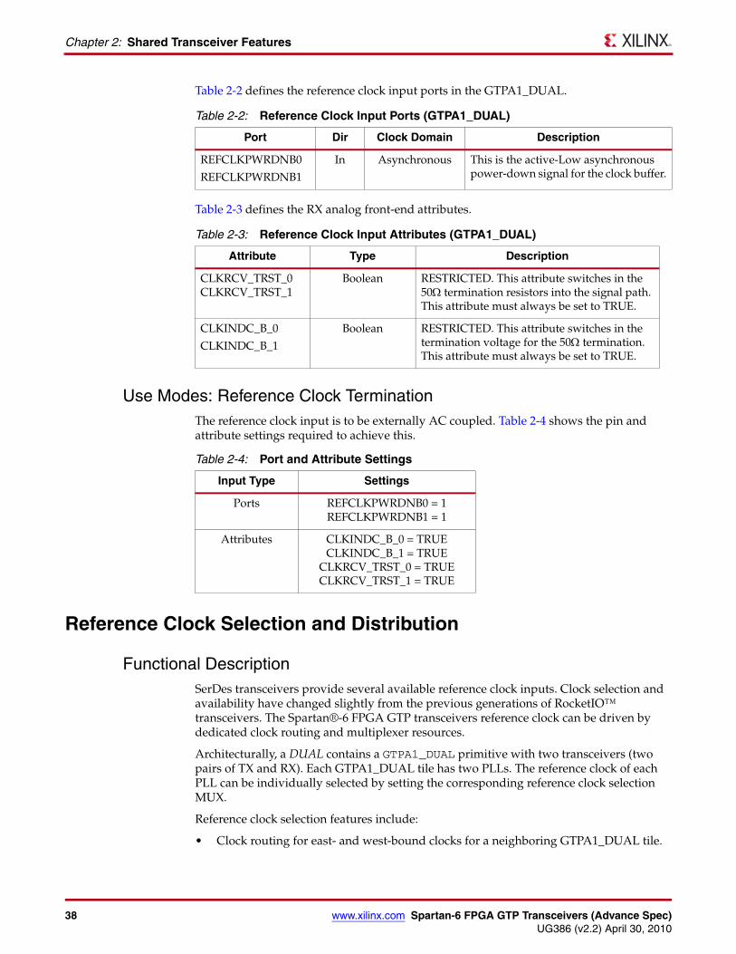
38 www.xilinx.com Spartan-6 FPGA GTP Transceivers (Advance Spec)UG386 (v2.2) April 30, 2010
Chapter 2: Shared Transceiver Features
Table 2-2 defines the reference clock input ports in the GTPA1_DUAL.
Table 2-3 defines the RX analog front-end attributes.
Use Modes: Reference Clock TerminationThe reference clock input is to be externally AC coupled. Table 2-4 shows the pin and attribute settings required to achieve this.
Reference Clock Selection and Distribution
Functional DescriptionSerDes transceivers provide several available reference clock inputs. Clock selection and availability have changed slightly from the previous generations of RocketIO™ transceivers. The Spartan®-6 FPGA GTP transceivers reference clock can be driven by dedicated clock routing and multiplexer resources.
Architecturally, a DUAL contains a GTPA1_DUAL primitive with two transceivers (two pairs of TX and RX). Each GTPA1_DUAL tile has two PLLs. The reference clock of each PLL can be individually selected by setting the corresponding reference clock selection MUX.
Reference clock selection features include:
• Clock routing for east- and west-bound clocks for a neighboring GTPA1_DUAL tile.
Table 2-2: Reference Clock Input Ports (GTPA1_DUAL)
Port Dir Clock Domain Description
REFCLKPWRDNB0
REFCLKPWRDNB1
In Asynchronous This is the active-Low asynchronous power-down signal for the clock buffer.
Table 2-3: Reference Clock Input Attributes (GTPA1_DUAL)
Attribute Type Description
CLKRCV_TRST_0 CLKRCV_TRST_1
Boolean RESTRICTED. This attribute switches in the 50Ω termination resistors into the signal path. This attribute must always be set to TRUE.
CLKINDC_B_0
CLKINDC_B_1
Boolean RESTRICTED. This attribute switches in the termination voltage for the 50Ω termination. This attribute must always be set to TRUE.
Table 2-4: Port and Attribute Settings
Input Type Settings
Ports REFCLKPWRDNB0 = 1 REFCLKPWRDNB1 = 1
Attributes CLKINDC_B_0 = TRUE CLKINDC_B_1 = TRUE
CLKRCV_TRST_0 = TRUE CLKRCV_TRST_1 = TRUE
Spartan-6 FPGA GTP Transceivers (Advance Spec) www.xilinx.com 39UG386 (v2.2) April 30, 2010
Reference Clock Selection and Distribution
• Clock inputs available per GTP PLL.
• Static or dynamic selection of the reference clock for the PLLs.
Figure 2-2 shows the GTPA1_DUAL architecture with two GTP transceivers, two dedicated reference clock pin pairs, and dedicated east/west reference clock routing. For each PLL within a GTPA1_DUAL tile, eight clock sources can be used as the reference clock source based on the reference clock MUX configurations:
• Two reference clock pin pairs from external pins
• CLK[0/1]0 for PLL0
• CLK[0/1]1 for PLL1
• Two reference clock pin pairs from the east and west:
• CLKINEAST0 and CLKINWEST0 for PLL0
• CLKINEAST1 and CLKINWEST1 for PLL1
If the neighboring GTPA1_DUAL tile does not exist, the corresponding port becomes a no connect and can be left floating.
• Two reference clocks pin pairs from the PLL of the FPGA logic:
• PLLCLK[0/1]0 for PLL0
• PLLCLK[0/1]1 for PLL1
• Two reference clock signals generated by the FPGA logic:
• GCLK[0/1]0 for PLL0
• GCLK[0/1]1 for PLL1
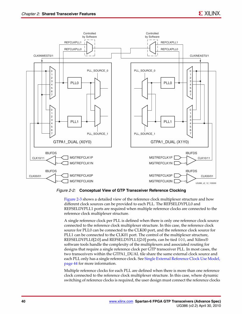
40 www.xilinx.com Spartan-6 FPGA GTP Transceivers (Advance Spec)UG386 (v2.2) April 30, 2010
Chapter 2: Shared Transceiver Features
Figure 2-3 shows a detailed view of the reference clock multiplexer structure and how different clock sources can be provided to each PLL. The REFSELDYPLL0 and REFSELDYPLL1 ports are required when multiple reference clocks are connected to the reference clock multiplexer structure.
A single reference clock per PLL is defined when there is only one reference clock source connected to the reference clock multiplexer structure. In this case, the reference clock source for PLL0 can be connected to the CLK00 port, and the reference clock source for PLL1 can be connected to the CLK01 port. The control of the multiplexer structure, REFSELDYPLL0[2:0] and REFSELDYPLL1[2:0] ports, can be tied 000, and Xilinx® software tools handle the complexity of the multiplexers and associated routing for designs that require a single reference clock per GTP transceiver PLL. In most cases, the two transceivers within the GTPA1_DUAL tile share the same external clock source and each PLL only has a single reference clock. See Single External Reference Clock Use Model, page 44 for more information.
Multiple reference clocks for each PLL are defined when there is more than one reference clock connected to the reference clock multiplexer structure. In this case, where dynamic switching of reference clocks is required, the user design must connect the reference clocks
X-Ref Target - Figure 2-2
Figure 2-2: Conceptual View of GTP Transceiver Reference Clocking
UG386_c2_12_103009
PLL_SOURCE_0
Controlledby Software
REFCLKPLL1
REFCLKPLL0
PLL_SOURCE_1
CLK10/11
PLL0
0
234567
1
MGTREFCLK1P
MGTREFCLK1N
IBUFDS
PLL1
CLK00/01 MGTREFCLK0P
MGTREFCLK0N
IBUFDS
0
234567
1
PLL_SOURCE_0
Controlledby Software
REFCLKPLL1
REFCLKPLL0
CLKINEAST0/1CLKINWEST0/1
PLL_SOURCE_1
CLK10/11
PLL0
0
234567
1
MGTREFCLK1P
MGTREFCLK1N
IBUFDS
PLL1
CLK00/01MGTREFCLK0P
MGTREFCLK0N
IBUFDS
0
234567
1
GTPA1_DUAL (X0Y0) GTPA1_DUAL (X1Y0)
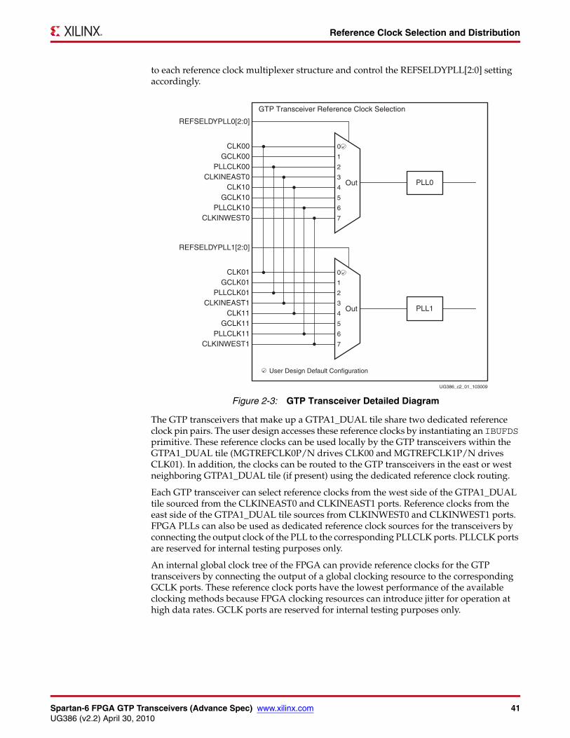
Spartan-6 FPGA GTP Transceivers (Advance Spec) www.xilinx.com 41UG386 (v2.2) April 30, 2010
Reference Clock Selection and Distribution
to each reference clock multiplexer structure and control the REFSELDYPLL[2:0] setting accordingly.
The GTP transceivers that make up a GTPA1_DUAL tile share two dedicated reference clock pin pairs. The user design accesses these reference clocks by instantiating an IBUFDS primitive. These reference clocks can be used locally by the GTP transceivers within the GTPA1_DUAL tile (MGTREFCLK0P/N drives CLK00 and MGTREFCLK1P/N drives CLK01). In addition, the clocks can be routed to the GTP transceivers in the east or west neighboring GTPA1_DUAL tile (if present) using the dedicated reference clock routing.
Each GTP transceiver can select reference clocks from the west side of the GTPA1_DUAL tile sourced from the CLKINEAST0 and CLKINEAST1 ports. Reference clocks from the east side of the GTPA1_DUAL tile sources from CLKINWEST0 and CLKINWEST1 ports. FPGA PLLs can also be used as dedicated reference clock sources for the transceivers by connecting the output clock of the PLL to the corresponding PLLCLK ports. PLLCLK ports are reserved for internal testing purposes only.
An internal global clock tree of the FPGA can provide reference clocks for the GTP transceivers by connecting the output of a global clocking resource to the corresponding GCLK ports. These reference clock ports have the lowest performance of the available clocking methods because FPGA clocking resources can introduce jitter for operation at high data rates. GCLK ports are reserved for internal testing purposes only.
X-Ref Target - Figure 2-3
Figure 2-3: GTP Transceiver Detailed Diagram
0
1
2
3
4
5
6
7
CLK00GCLK00
PLLCLK00CLKINEAST0
CLK10GCLK10
PLLCLK10CLKINWEST0
REFSELDYPLL0[2:0]
Out
UG386_c2_01_103009
PLL0
0
1
2
3
4
5
6
7
CLK01GCLK01
PLLCLK01CLKINEAST1
CLK11GCLK11
PLLCLK11CLKINWEST1
REFSELDYPLL1[2:0]
Out
User Design Default Configuration
PLL1
GTP Transceiver Reference Clock Selection
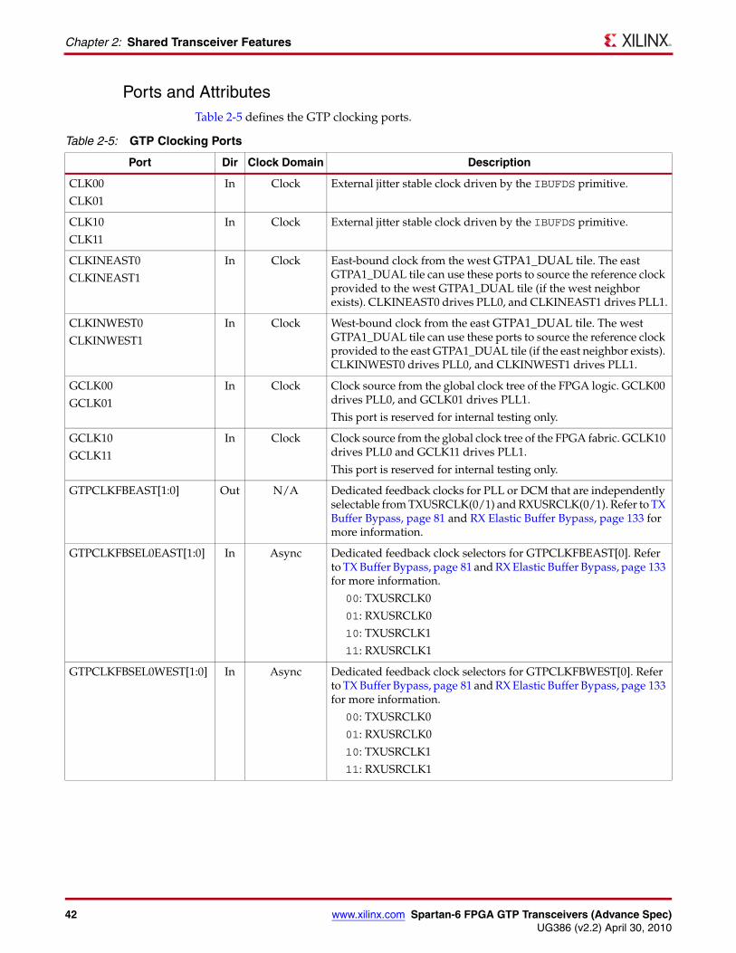
42 www.xilinx.com Spartan-6 FPGA GTP Transceivers (Advance Spec)UG386 (v2.2) April 30, 2010
Chapter 2: Shared Transceiver Features
Ports and AttributesTable 2-5 defines the GTP clocking ports.
Table 2-5: GTP Clocking Ports
Port Dir Clock Domain Description
CLK00
CLK01
In Clock External jitter stable clock driven by the IBUFDS primitive.
CLK10
CLK11
In Clock External jitter stable clock driven by the IBUFDS primitive.
CLKINEAST0
CLKINEAST1
In Clock East-bound clock from the west GTPA1_DUAL tile. The east GTPA1_DUAL tile can use these ports to source the reference clock provided to the west GTPA1_DUAL tile (if the west neighbor exists). CLKINEAST0 drives PLL0, and CLKINEAST1 drives PLL1.
CLKINWEST0
CLKINWEST1
In Clock West-bound clock from the east GTPA1_DUAL tile. The west GTPA1_DUAL tile can use these ports to source the reference clock provided to the east GTPA1_DUAL tile (if the east neighbor exists). CLKINWEST0 drives PLL0, and CLKINWEST1 drives PLL1.
GCLK00
GCLK01
In Clock Clock source from the global clock tree of the FPGA logic. GCLK00 drives PLL0, and GCLK01 drives PLL1.
This port is reserved for internal testing only.
GCLK10
GCLK11
In Clock Clock source from the global clock tree of the FPGA fabric. GCLK10 drives PLL0 and GCLK11 drives PLL1.
This port is reserved for internal testing only.
GTPCLKFBEAST[1:0] Out N/A Dedicated feedback clocks for PLL or DCM that are independently selectable from TXUSRCLK(0/1) and RXUSRCLK(0/1). Refer to TX Buffer Bypass, page 81 and RX Elastic Buffer Bypass, page 133 for more information.
GTPCLKFBSEL0EAST[1:0] In Async Dedicated feedback clock selectors for GTPCLKFBEAST[0]. Refer to TX Buffer Bypass, page 81 and RX Elastic Buffer Bypass, page 133 for more information.
00: TXUSRCLK0
01: RXUSRCLK0
10: TXUSRCLK1
11: RXUSRCLK1
GTPCLKFBSEL0WEST[1:0] In Async Dedicated feedback clock selectors for GTPCLKFBWEST[0]. Refer to TX Buffer Bypass, page 81 and RX Elastic Buffer Bypass, page 133 for more information.
00: TXUSRCLK0
01: RXUSRCLK0
10: TXUSRCLK1
11: RXUSRCLK1
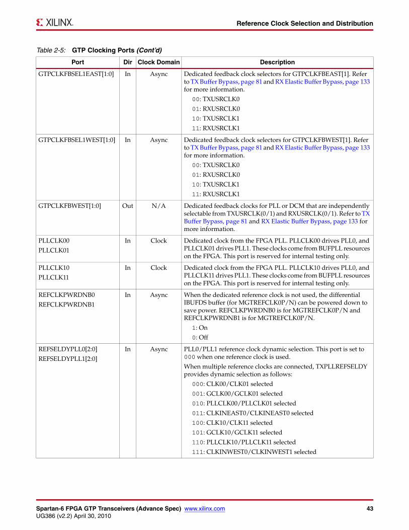
Spartan-6 FPGA GTP Transceivers (Advance Spec) www.xilinx.com 43UG386 (v2.2) April 30, 2010
Reference Clock Selection and Distribution
GTPCLKFBSEL1EAST[1:0] In Async Dedicated feedback clock selectors for GTPCLKFBEAST[1]. Refer to TX Buffer Bypass, page 81 and RX Elastic Buffer Bypass, page 133 for more information.
00: TXUSRCLK0
01: RXUSRCLK0
10: TXUSRCLK1
11: RXUSRCLK1
GTPCLKFBSEL1WEST[1:0] In Async Dedicated feedback clock selectors for GTPCLKFBWEST[1]. Refer to TX Buffer Bypass, page 81 and RX Elastic Buffer Bypass, page 133 for more information.
00: TXUSRCLK0
01: RXUSRCLK0
10: TXUSRCLK1
11: RXUSRCLK1
GTPCLKFBWEST[1:0] Out N/A Dedicated feedback clocks for PLL or DCM that are independently selectable from TXUSRCLK(0/1) and RXUSRCLK(0/1). Refer to TX Buffer Bypass, page 81 and RX Elastic Buffer Bypass, page 133 for more information.
PLLCLK00
PLLCLK01
In Clock Dedicated clock from the FPGA PLL. PLLCLK00 drives PLL0, and PLLCLK01 drives PLL1. These clocks come from BUFPLL resources on the FPGA. This port is reserved for internal testing only.
PLLCLK10
PLLCLK11
In Clock Dedicated clock from the FPGA PLL. PLLCLK10 drives PLL0, and PLLCLK11 drives PLL1. These clocks come from BUFPLL resources on the FPGA. This port is reserved for internal testing only.
REFCLKPWRDNB0
REFCLKPWRDNB1
In Async When the dedicated reference clock is not used, the differential IBUFDS buffer (for MGTREFCLK0P/N) can be powered down to save power. REFCLKPWRDNB0 is for MGTREFCLK0P/N and REFCLKPWRDNB1 is for MGTREFCLK0P/N.
1: On
0: Off
REFSELDYPLL0[2:0]
REFSELDYPLL1[2:0]
In Async PLL0/PLL1 reference clock dynamic selection. This port is set to 000 when one reference clock is used.
When multiple reference clocks are connected, TXPLLREFSELDY provides dynamic selection as follows:
000: CLK00/CLK01 selected
001: GCLK00/GCLK01 selected
010: PLLCLK00/PLLCLK01 selected
011: CLKINEAST0/CLKINEAST0 selected
100: CLK10/CLK11 selected
101: GCLK10/GCLK11 selected
110: PLLCLK10/PLLCLK11 selected
111: CLKINWEST0/CLKINWEST1 selected
Table 2-5: GTP Clocking Ports (Cont’d)
Port Dir Clock Domain Description
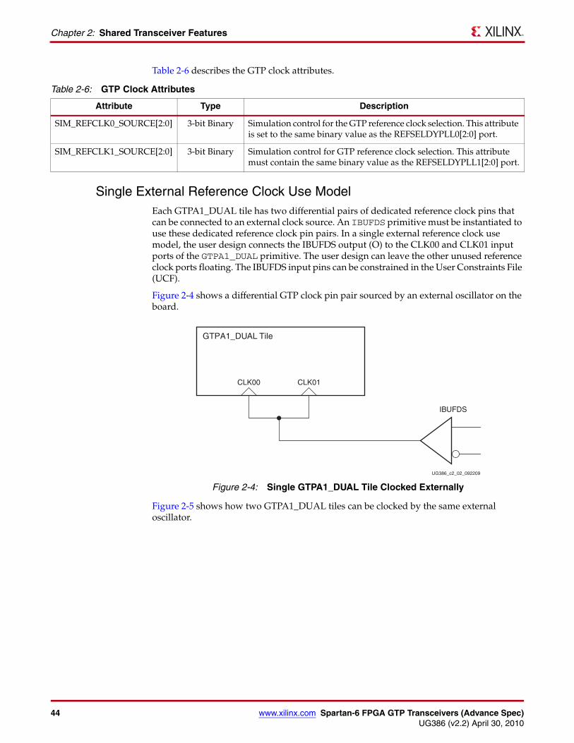
44 www.xilinx.com Spartan-6 FPGA GTP Transceivers (Advance Spec)UG386 (v2.2) April 30, 2010
Chapter 2: Shared Transceiver Features
Table 2-6 describes the GTP clock attributes.
Single External Reference Clock Use ModelEach GTPA1_DUAL tile has two differential pairs of dedicated reference clock pins that can be connected to an external clock source. An IBUFDS primitive must be instantiated to use these dedicated reference clock pin pairs. In a single external reference clock use model, the user design connects the IBUFDS output (O) to the CLK00 and CLK01 input ports of the GTPA1_DUAL primitive. The user design can leave the other unused reference clock ports floating. The IBUFDS input pins can be constrained in the User Constraints File (UCF).
Figure 2-4 shows a differential GTP clock pin pair sourced by an external oscillator on the board.
Figure 2-5 shows how two GTPA1_DUAL tiles can be clocked by the same external oscillator.
Table 2-6: GTP Clock Attributes
Attribute Type Description
SIM_REFCLK0_SOURCE[2:0] 3-bit Binary Simulation control for the GTP reference clock selection. This attribute is set to the same binary value as the REFSELDYPLL0[2:0] port.
SIM_REFCLK1_SOURCE[2:0] 3-bit Binary Simulation control for GTP reference clock selection. This attribute must contain the same binary value as the REFSELDYPLL1[2:0] port.
X-Ref Target - Figure 2-4
Figure 2-4: Single GTPA1_DUAL Tile Clocked Externally
CLK00 CLK01
IBUFDS
UG386_c2_02_092209
GTPA1_DUAL Tile
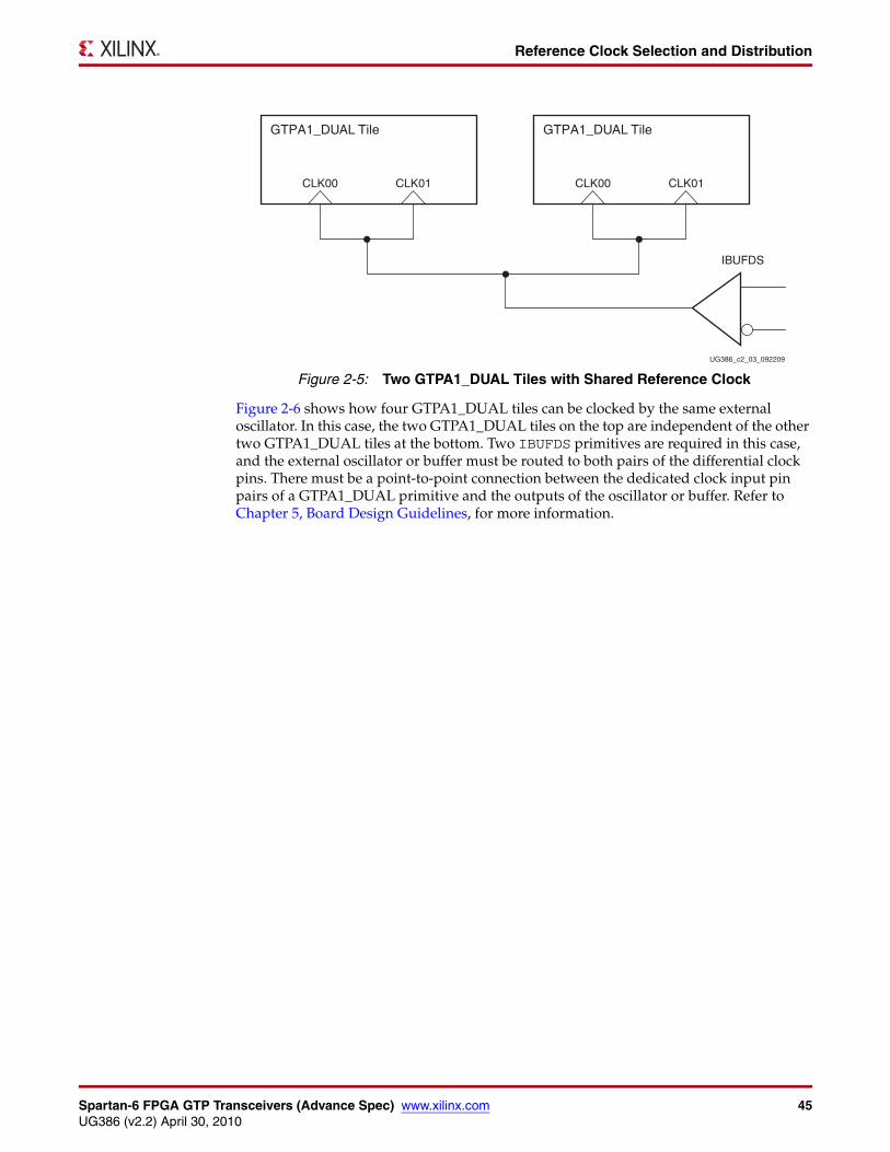
Spartan-6 FPGA GTP Transceivers (Advance Spec) www.xilinx.com 45UG386 (v2.2) April 30, 2010
Reference Clock Selection and Distribution
Figure 2-6 shows how four GTPA1_DUAL tiles can be clocked by the same external oscillator. In this case, the two GTPA1_DUAL tiles on the top are independent of the other two GTPA1_DUAL tiles at the bottom. Two IBUFDS primitives are required in this case, and the external oscillator or buffer must be routed to both pairs of the differential clock pins. There must be a point-to-point connection between the dedicated clock input pin pairs of a GTPA1_DUAL primitive and the outputs of the oscillator or buffer. Refer to Chapter 5, Board Design Guidelines, for more information.
X-Ref Target - Figure 2-5
Figure 2-5: Two GTPA1_DUAL Tiles with Shared Reference Clock
CLK00 CLK01
IBUFDS
UG386_c2_03_092209
GTPA1_DUAL Tile
CLK00 CLK01
GTPA1_DUAL Tile
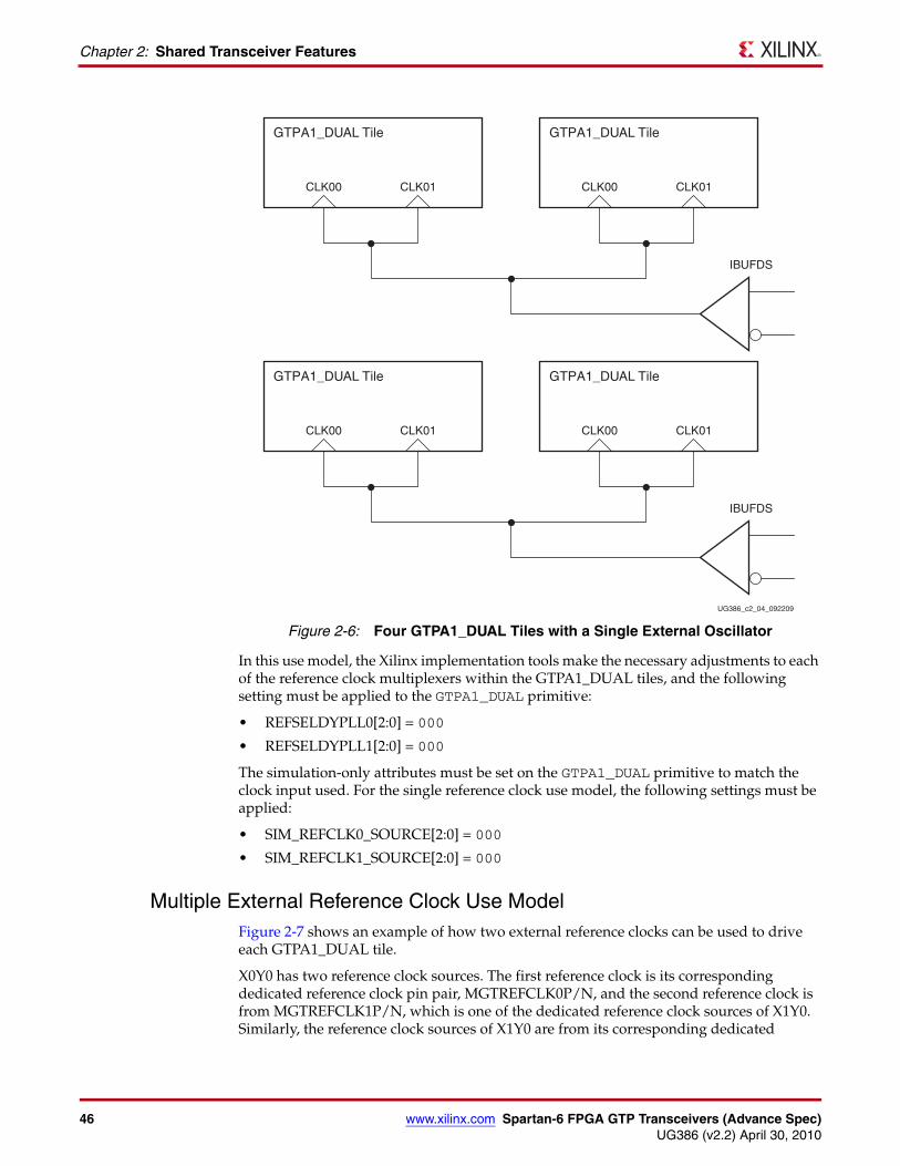
46 www.xilinx.com Spartan-6 FPGA GTP Transceivers (Advance Spec)UG386 (v2.2) April 30, 2010
Chapter 2: Shared Transceiver Features
In this use model, the Xilinx implementation tools make the necessary adjustments to each of the reference clock multiplexers within the GTPA1_DUAL tiles, and the following setting must be applied to the GTPA1_DUAL primitive:
• REFSELDYPLL0[2:0] = 000
• REFSELDYPLL1[2:0] = 000
The simulation-only attributes must be set on the GTPA1_DUAL primitive to match the clock input used. For the single reference clock use model, the following settings must be applied:
• SIM_REFCLK0_SOURCE[2:0] = 000
• SIM_REFCLK1_SOURCE[2:0] = 000
Multiple External Reference Clock Use ModelFigure 2-7 shows an example of how two external reference clocks can be used to drive each GTPA1_DUAL tile.
X0Y0 has two reference clock sources. The first reference clock is its corresponding dedicated reference clock pin pair, MGTREFCLK0P/N, and the second reference clock is from MGTREFCLK1P/N, which is one of the dedicated reference clock sources of X1Y0. Similarly, the reference clock sources of X1Y0 are from its corresponding dedicated
X-Ref Target - Figure 2-6
Figure 2-6: Four GTPA1_DUAL Tiles with a Single External Oscillator
CLK00 CLK01
IBUFDS
UG386_c2_04_092209
GTPA1_DUAL Tile
CLK00 CLK01
GTPA1_DUAL Tile
CLK00 CLK01
IBUFDS
GTPA1_DUAL Tile
CLK00 CLK01
GTPA1_DUAL Tile
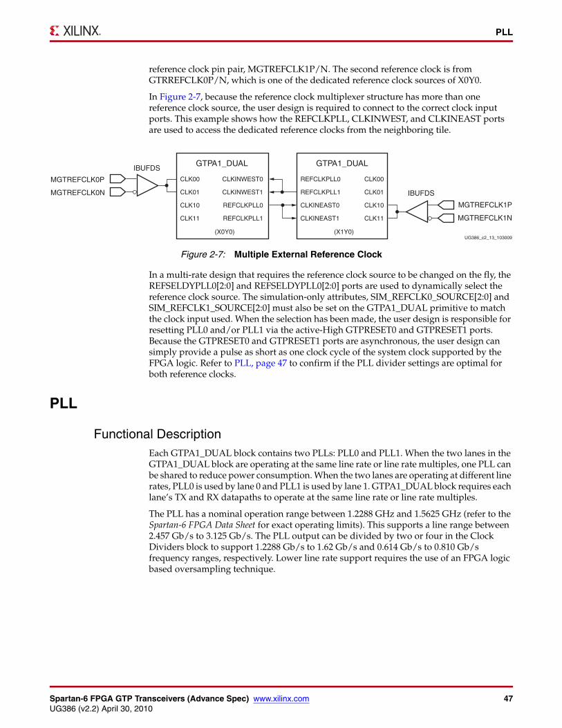
Spartan-6 FPGA GTP Transceivers (Advance Spec) www.xilinx.com 47UG386 (v2.2) April 30, 2010
PLL
reference clock pin pair, MGTREFCLK1P/N. The second reference clock is from GTRREFCLK0P/N, which is one of the dedicated reference clock sources of X0Y0.
In Figure 2-7, because the reference clock multiplexer structure has more than one reference clock source, the user design is required to connect to the correct clock input ports. This example shows how the REFCLKPLL, CLKINWEST, and CLKINEAST ports are used to access the dedicated reference clocks from the neighboring tile.
In a multi-rate design that requires the reference clock source to be changed on the fly, the REFSELDYPLL0[2:0] and REFSELDYPLL0[2:0] ports are used to dynamically select the reference clock source. The simulation-only attributes, SIM_REFCLK0_SOURCE[2:0] and SIM_REFCLK1_SOURCE[2:0] must also be set on the GTPA1_DUAL primitive to match the clock input used. When the selection has been made, the user design is responsible for resetting PLL0 and/or PLL1 via the active-High GTPRESET0 and GTPRESET1 ports. Because the GTPRESET0 and GTPRESET1 ports are asynchronous, the user design can simply provide a pulse as short as one clock cycle of the system clock supported by the FPGA logic. Refer to PLL, page 47 to confirm if the PLL divider settings are optimal for both reference clocks.
PLL
Functional DescriptionEach GTPA1_DUAL block contains two PLLs: PLL0 and PLL1. When the two lanes in the GTPA1_DUAL block are operating at the same line rate or line rate multiples, one PLL can be shared to reduce power consumption. When the two lanes are operating at different line rates, PLL0 is used by lane 0 and PLL1 is used by lane 1. GTPA1_DUAL block requires each lane’s TX and RX datapaths to operate at the same line rate or line rate multiples.
The PLL has a nominal operation range between 1.2288 GHz and 1.5625 GHz (refer to the Spartan-6 FPGA Data Sheet for exact operating limits). This supports a line range between 2.457 Gb/s to 3.125 Gb/s. The PLL output can be divided by two or four in the Clock Dividers block to support 1.2288 Gb/s to 1.62 Gb/s and 0.614 Gb/s to 0.810 Gb/s frequency ranges, respectively. Lower line rate support requires the use of an FPGA logic based oversampling technique.
X-Ref Target - Figure 2-7
Figure 2-7: Multiple External Reference Clock
UG386_c2_13_103009
GTPA1_DUAL
(X0Y0)
MGTREFCLK1P
MGTREFCLK1N
IBUFDS
CLK00
CLK01
CLK10
CLK11
CLKINWEST0
CLKINWEST1
REFCLKPLL0
REFCLKPLL1
GTPA1_DUAL
(X1Y0)
CLK00
CLK01
CLK10
CLK11
REFCLKPLL0
REFCLKPLL1
CLKINEAST0
CLKINEAST1
MGTREFCLK0P
MGTREFCLK0N
IBUFDS
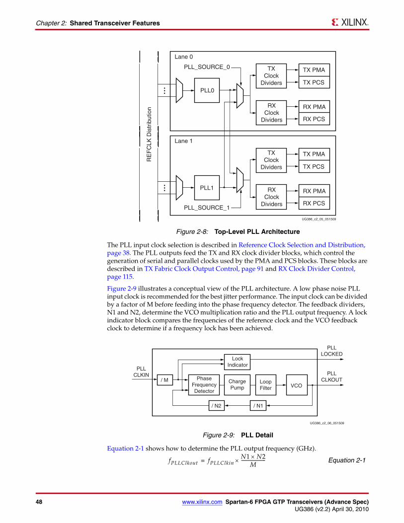
48 www.xilinx.com Spartan-6 FPGA GTP Transceivers (Advance Spec)UG386 (v2.2) April 30, 2010
Chapter 2: Shared Transceiver Features
The PLL input clock selection is described in Reference Clock Selection and Distribution, page 38. The PLL outputs feed the TX and RX clock divider blocks, which control the generation of serial and parallel clocks used by the PMA and PCS blocks. These blocks are described in TX Fabric Clock Output Control, page 91 and RX Clock Divider Control, page 115.
Figure 2-9 illustrates a conceptual view of the PLL architecture. A low phase noise PLL input clock is recommended for the best jitter performance. The input clock can be divided by a factor of M before feeding into the phase frequency detector. The feedback dividers, N1 and N2, determine the VCO multiplication ratio and the PLL output frequency. A lock indicator block compares the frequencies of the reference clock and the VCO feedback clock to determine if a frequency lock has been achieved.
Equation 2-1 shows how to determine the PLL output frequency (GHz).
Equation 2-1
X-Ref Target - Figure 2-8
Figure 2-8: Top-Level PLL Architecture
X-Ref Target - Figure 2-9
Figure 2-9: PLL Detail
RE
FC
LK D
istr
ibut
ion
PLL0
TXClock
Dividers
RXClock
Dividers
TX PMA
Lane 0
TX PCS
RX PMA
RX PCS
UG386_c2_05_051509
PLL1
PLL_SOURCE_1
PLL_SOURCE_0
TXClock
Dividers
RXClock
Dividers
TX PMA
Lane 1
TX PCS
RX PMA
RX PCS
PLLCLKIN
/ M
LockIndicator
PhaseFrequencyDetector
ChargePump
LoopFilter VCO
PLLLOCKED
PLLCLKOUT
/ N1/ N2
UG386_c2_06_051509
fPLLClkout fPLLClkinN1 N2×
M----------------------×=
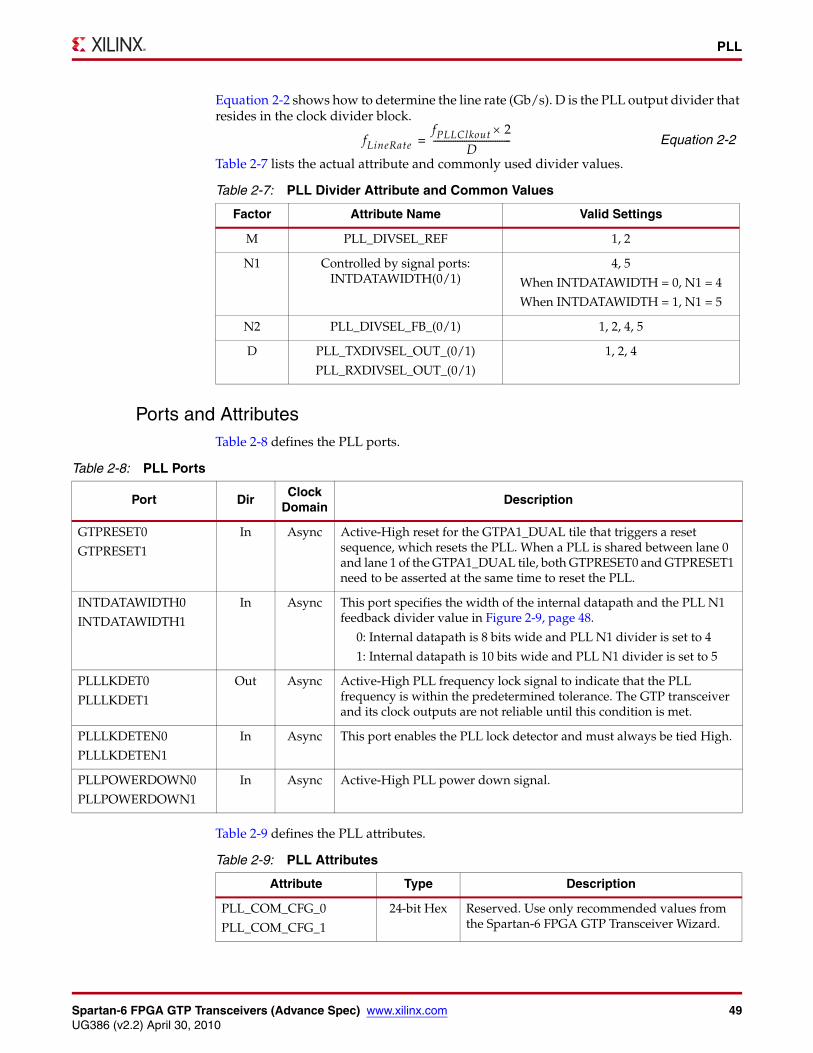
Spartan-6 FPGA GTP Transceivers (Advance Spec) www.xilinx.com 49UG386 (v2.2) April 30, 2010
PLL
Equation 2-2 shows how to determine the line rate (Gb/s). D is the PLL output divider that resides in the clock divider block.
Equation 2-2
Table 2-7 lists the actual attribute and commonly used divider values.
Ports and AttributesTable 2-8 defines the PLL ports.
Table 2-9 defines the PLL attributes.
Table 2-7: PLL Divider Attribute and Common Values
Factor Attribute Name Valid Settings
M PLL_DIVSEL_REF 1, 2
N1 Controlled by signal ports: INTDATAWIDTH(0/1)
4, 5
When INTDATAWIDTH = 0, N1 = 4
When INTDATAWIDTH = 1, N1 = 5
N2 PLL_DIVSEL_FB_(0/1) 1, 2, 4, 5
D PLL_TXDIVSEL_OUT_(0/1)
PLL_RXDIVSEL_OUT_(0/1)
1, 2, 4
fLineRatefPLLClkout 2×
D-----------------------------------=
Table 2-8: PLL Ports
Port DirClock
DomainDescription
GTPRESET0
GTPRESET1
In Async Active-High reset for the GTPA1_DUAL tile that triggers a reset sequence, which resets the PLL. When a PLL is shared between lane 0 and lane 1 of the GTPA1_DUAL tile, both GTPRESET0 and GTPRESET1 need to be asserted at the same time to reset the PLL.
INTDATAWIDTH0
INTDATAWIDTH1
In Async This port specifies the width of the internal datapath and the PLL N1 feedback divider value in Figure 2-9, page 48.
0: Internal datapath is 8 bits wide and PLL N1 divider is set to 4
1: Internal datapath is 10 bits wide and PLL N1 divider is set to 5
PLLLKDET0
PLLLKDET1
Out Async Active-High PLL frequency lock signal to indicate that the PLL frequency is within the predetermined tolerance. The GTP transceiver and its clock outputs are not reliable until this condition is met.
PLLLKDETEN0
PLLLKDETEN1
In Async This port enables the PLL lock detector and must always be tied High.
PLLPOWERDOWN0
PLLPOWERDOWN1
In Async Active-High PLL power down signal.
Table 2-9: PLL Attributes
Attribute Type Description
PLL_COM_CFG_0
PLL_COM_CFG_1
24-bit Hex Reserved. Use only recommended values from the Spartan-6 FPGA GTP Transceiver Wizard.
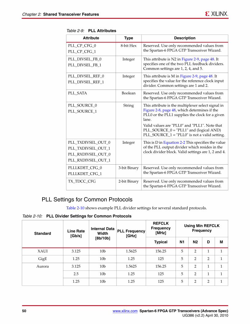
50 www.xilinx.com Spartan-6 FPGA GTP Transceivers (Advance Spec)UG386 (v2.2) April 30, 2010
Chapter 2: Shared Transceiver Features
PLL Settings for Common ProtocolsTable 2-10 shows example PLL divider settings for several standard protocols.
PLL_CP_CFG_0
PLL_CP_CFG_1
8-bit Hex Reserved. Use only recommended values from the Spartan-6 FPGA GTP Transceiver Wizard.
PLL_DIVSEL_FB_0
PLL_DIVSEL_FB_1
Integer This attribute is N2 in Figure 2-9, page 48. It specifies one of the two PLL feedback dividers. Common settings are 1, 2, 4, and 5.
PLL_DIVSEL_REF_0
PLL_DIVSEL_REF_1
Integer This attribute is M in Figure 2-9, page 48. It specifies the value for the reference clock input divider. Common settings are 1 and 2.
PLL_SATA Boolean Reserved. Use only recommended values from the Spartan-6 FPGA GTP Transceiver Wizard.
PLL_SOURCE_0
PLL_SOURCE_1
String This attribute is the multiplexer select signal in Figure 2-8, page 48, which determines if the PLL0 or the PLL1 supplies the clock for a given lane.
Valid values are "PLL0" and "PLL1". Note that PLL_SOURCE_0 = "PLL1" and (logical AND) PLL_SOURCE_1 = "PLL0" is not a valid setting.
PLL_TXDIVSEL_OUT_0
PLL_TXDIVSEL_OUT_1
PLL_RXDIVSEL_OUT_0
PLL_RXDIVSEL_OUT_1
Integer This is D in Equation 2-2 This specifies the value of the PLL output divider which resides in the clock divider block. Valid settings are 1, 2 and 4.
PLLLKDET_CFG_0
PLLLKDET_CFG_1
3-bit Binary Reserved. Use only recommended values from the Spartan-6 FPGA GTP Transceiver Wizard.
TX_TDCC_CFG 2-bit Binary Reserved. Use only recommended values from the Spartan-6 FPGA GTP Transceiver Wizard.
Table 2-9: PLL Attributes
Attribute Type Description
Table 2-10: PLL Divider Settings for Common Protocols
StandardLine Rate
[Gb/s]
Internal Data Width
[8b/10b]
PLL Frequency[GHz]
REFCLK Frequency
[MHz]
Using Min REFCLK Frequency
Typical N1 N2 D M
XAUI 3.125 10b 1.5625 156.25 5 2 1 1
GigE 1.25 10b 1.25 125 5 2 2 1
Aurora 3.125 10b 1.5625 156.25 5 2 1 1
2.5 10b 1.25 125 5 2 1 1
1.25 10b 1.25 125 5 2 2 1
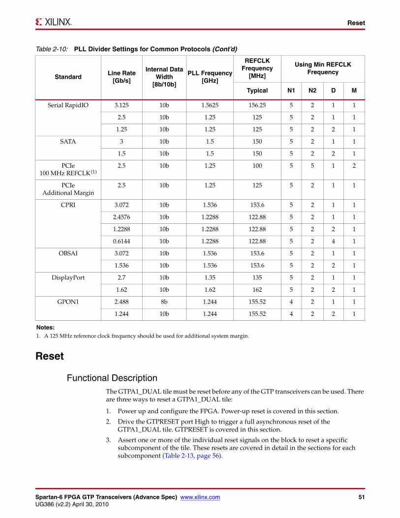
Spartan-6 FPGA GTP Transceivers (Advance Spec) www.xilinx.com 51UG386 (v2.2) April 30, 2010
Reset
Reset
Functional DescriptionThe GTPA1_DUAL tile must be reset before any of the GTP transceivers can be used. There are three ways to reset a GTPA1_DUAL tile:
1. Power up and configure the FPGA. Power-up reset is covered in this section.
2. Drive the GTPRESET port High to trigger a full asynchronous reset of the GTPA1_DUAL tile. GTPRESET is covered in this section.
3. Assert one or more of the individual reset signals on the block to reset a specific subcomponent of the tile. These resets are covered in detail in the sections for each subcomponent (Table 2-13, page 56).
Serial RapidIO 3.125 10b 1.5625 156.25 5 2 1 1
2.5 10b 1.25 125 5 2 1 1
1.25 10b 1.25 125 5 2 2 1
SATA 3 10b 1.5 150 5 2 1 1
1.5 10b 1.5 150 5 2 2 1
PCIe100 MHz REFCLK(1)
2.5 10b 1.25 100 5 5 1 2
PCIeAdditional Margin
2.5 10b 1.25 125 5 2 1 1
CPRI 3.072 10b 1.536 153.6 5 2 1 1
2.4576 10b 1.2288 122.88 5 2 1 1
1.2288 10b 1.2288 122.88 5 2 2 1
0.6144 10b 1.2288 122.88 5 2 4 1
OBSAI 3.072 10b 1.536 153.6 5 2 1 1
1.536 10b 1.536 153.6 5 2 2 1
DisplayPort 2.7 10b 1.35 135 5 2 1 1
1.62 10b 1.62 162 5 2 2 1
GPON1 2.488 8b 1.244 155.52 4 2 1 1
1.244 10b 1.244 155.52 4 2 2 1
Notes: 1. A 125 MHz reference clock frequency should be used for additional system margin.
Table 2-10: PLL Divider Settings for Common Protocols (Cont’d)
StandardLine Rate
[Gb/s]
Internal Data Width
[8b/10b]
PLL Frequency[GHz]
REFCLK Frequency
[MHz]
Using Min REFCLK Frequency
Typical N1 N2 D M
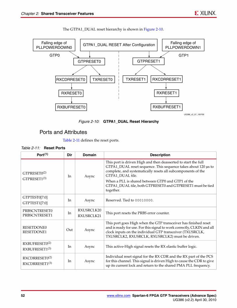
52 www.xilinx.com Spartan-6 FPGA GTP Transceivers (Advance Spec)UG386 (v2.2) April 30, 2010
Chapter 2: Shared Transceiver Features
The GTPA1_DUAL reset hierarchy is shown in Figure 2-10.
Ports and AttributesTable 2-11 defines the reset ports.
X-Ref Target - Figure 2-10
Figure 2-10: GTPA1_DUAL Reset Hierarchy
GTPA1_DUAL RESET After Configuration
GTP1GTP0
UG386_c2_07_100709
TXRESET1 RXCDRRESET1
RXRESET1
RXBUFRESET1
TXRESET0RXCDRRESET0
RXRESET0
RXBUFRESET0
GTPRESET0 GTPRESET1
Falling edge ofPLLPOWERDOWN1
Falling edge ofPLLPOWERDOWN0
Table 2-11: Reset Ports
Port(1) Dir Domain Description
GTPRESET0(2)
GTPRESET1(3) In Async
This port is driven High and then deasserted to start the full GTPA1_DUAL reset sequence. This sequence takes about 120 µs to complete, and systematically resets all subcomponents of the GTPA1_DUAL tile.
When a PLL is shared between GTP0 and GTP1 of the GTPA1_DUAL tile, both GTPRESET0 and GTPRESET1 must be tied together.
GTPTEST0[7:0]
GTPTEST1[7:0]In Async Reserved. Tied to 00010000.
PRBSCNTRESET0 PRBSCNTRESET1
InRXUSRCLK20
RXUSRCLK21This port resets the PRBS error counter.
RESETDONE0 RESETDONE1
Out Async
This port goes High when the GTP transceiver has finished reset and is ready for use. For this signal to work correctly, CLKIN and all clock inputs on the individual GTP transceiver (TXUSRCLK, TXUSRCLK2, RXUSRCLK, RXUSRCLK2) must be driven.
RXBUFRESET0(2)
RXBUFRESET1(3) In Async This active-High signal resets the RX elastic buffer logic.
RXCDRRESET0(2)
RXCDRRESET1(3) In AsyncIndividual reset signal for the RX CDR and the RX part of the PCS for this channel. This signal is driven High to cause the CDR to give up its current lock and return to the shared PMA PLL frequency.
Spartan-6 FPGA GTP Transceivers (Advance Spec) www.xilinx.com 53UG386 (v2.2) April 30, 2010
Reset
Table 2-12 defines the reset attributes.
RXRESET0(2)
RXRESET1(3) In Async Active-High reset for the RX PCS logic.
TXRESET0(2)
TXRESET1(3) In AsyncResets the PCS of the GTP transmitter, including the phase adjust FIFO, the 8B/10B encoder, and the FPGA TX interface.
Notes: 1. Ports that end in 0 and 1 are specific to GTP0 and GTP1, respectively.2. When these resets are active, RESETDONE0 is driven Low. All resets are asynchronous, positive-edge triggered, and synchronized
internally to a specific clock domain. The assertion of any of these resets causes the internal reset FSM to be held in the reset state until these resets are deasserted.
3. When these resets are active, RESETDONE1 is driven Low. All resets are asynchronous, positive-edge triggered, and synchronized internally to a specific clock domain. The assertion of any of these resets causes the internal reset FSM to be held in the reset state until these resets are deasserted.
Table 2-11: Reset Ports (Cont’d)
Port(1) Dir Domain Description
Table 2-12: Reset Attributes
Attribute(1) Type Description
CDR_PH_ADJ_TIME_0[4:0]
CDR_PH_ADJ_TIME_1[4:0]
5-bit Binary Sets time to wait after deassertion of CDR phase reset before completion of optional reset sequence for PCI Express® operation during electrical idle.
RX_EN_IDLE_HOLD_CDR_0
RX_EN_IDLE_HOLD_CDR_1
Boolean Enables CDR to hold its data during optional reset sequence for PCI Express operation during electrical idle.
RX_EN_IDLE_RESET_BUF_0
RX_EN_IDLE_RESET_BUF_1
Boolean When TRUE, the elastic buffer is reset if a valid signal is not present on the RX inputs. Works in conjunction with attributes RX_IDLE_HI_CNT_0, RX_IDLE_HI_CNT_1, RX_IDLE_LO_CNT_0, and RX_IDLE_LO_CNT_1.
RX_EN_IDLE_RESET_PH_0
RX_EN_IDLE_RESET_PH_1
Boolean Enables reset of CDR phase circuits during optional reset sequence for PCI Express operation during electrical idle.
RX_EN_IDLE_RESET_FR_0
RX_EN_IDLE_RESET_FR_1
Boolean Enables reset of CDR frequency circuits during optional reset sequence for PCI Express operation during electrical idle.
RX_EN_MODE_RESET_BUF_0
RX_EN_MODE_RESET_BUF_1
Boolean Enables automatic reset of the RX elastic buffer when the RXCHBONDMASTER(0/1) or RXCHBONDSLAVE(0/1) ports change. See RX Channel Bonding, page 149.
RX_IDLE_HI_CNT_0[3:0]
RX_IDLE_HI_CNT_1[3:0]
4-bit Binary Programmable counters used in association with resetting the RX elastic buffer in response to the absence of valid data on the RX inputs. Determines how long the RX inputs must remain in electrical idle before the elastic buffer reset is asserted.
RX_IDLE_LO_CNT_0[3:0]
RX_IDLE_LO_CNT_1[3:0]
4-bit Binary Programmable counters associated with deasserting the reset condition of the elastic buffer in response to the detection of valid data on the RX inputs. Determines how long the RX inputs must have good data (not be in electrical idle) before elastic buffer reset is deasserted.
Notes: 1. Attributes that end in _0 and _1 are specific to GTP0 and GTP1, respectively.
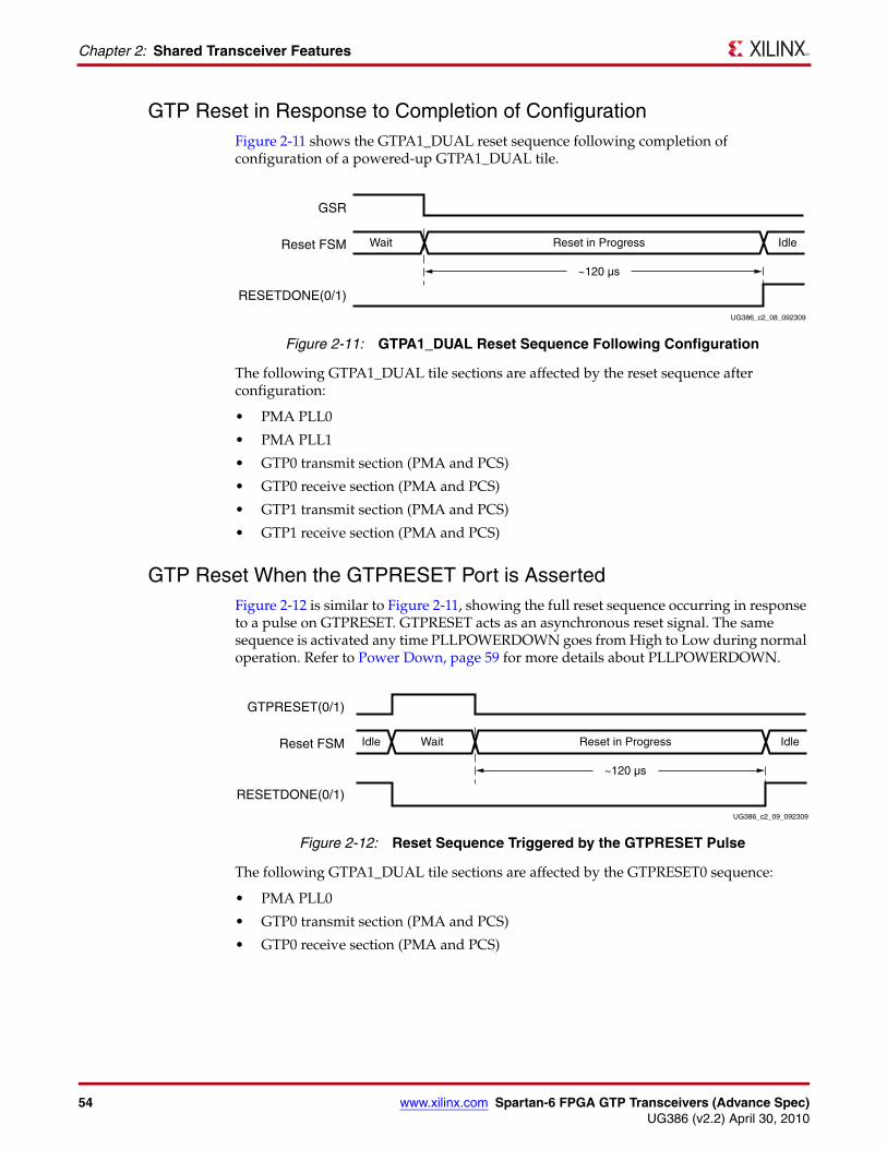
54 www.xilinx.com Spartan-6 FPGA GTP Transceivers (Advance Spec)UG386 (v2.2) April 30, 2010
Chapter 2: Shared Transceiver Features
GTP Reset in Response to Completion of ConfigurationFigure 2-11 shows the GTPA1_DUAL reset sequence following completion of configuration of a powered-up GTPA1_DUAL tile.
The following GTPA1_DUAL tile sections are affected by the reset sequence after configuration:
• PMA PLL0
• PMA PLL1
• GTP0 transmit section (PMA and PCS)
• GTP0 receive section (PMA and PCS)
• GTP1 transmit section (PMA and PCS)
• GTP1 receive section (PMA and PCS)
GTP Reset When the GTPRESET Port is AssertedFigure 2-12 is similar to Figure 2-11, showing the full reset sequence occurring in response to a pulse on GTPRESET. GTPRESET acts as an asynchronous reset signal. The same sequence is activated any time PLLPOWERDOWN goes from High to Low during normal operation. Refer to Power Down, page 59 for more details about PLLPOWERDOWN.
The following GTPA1_DUAL tile sections are affected by the GTPRESET0 sequence:
• PMA PLL0
• GTP0 transmit section (PMA and PCS)
• GTP0 receive section (PMA and PCS)
X-Ref Target - Figure 2-11
Figure 2-11: GTPA1_DUAL Reset Sequence Following Configuration
RESETDONE(0/1)
Reset FSM
GSR
Wait Reset in Progress
~120 µs
Idle
UG386_c2_08_092309
X-Ref Target - Figure 2-12
Figure 2-12: Reset Sequence Triggered by the GTPRESET Pulse
RESETDONE(0/1)
Reset FSM
GTPRESET(0/1)
Wait Reset in Progress
~120 µs
Idle
UG386_c2_09_092309
Idle
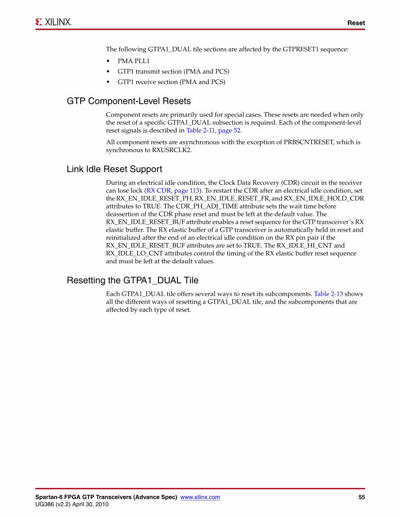
Spartan-6 FPGA GTP Transceivers (Advance Spec) www.xilinx.com 55UG386 (v2.2) April 30, 2010
Reset
The following GTPA1_DUAL tile sections are affected by the GTPRESET1 sequence:
• PMA PLL1
• GTP1 transmit section (PMA and PCS)
• GTP1 receive section (PMA and PCS)
GTP Component-Level ResetsComponent resets are primarily used for special cases. These resets are needed when only the reset of a specific GTPA1_DUAL subsection is required. Each of the component-level reset signals is described in Table 2-11, page 52.
All component resets are asynchronous with the exception of PRBSCNTRESET, which is synchronous to RXUSRCLK2.
Link Idle Reset SupportDuring an electrical idle condition, the Clock Data Recovery (CDR) circuit in the receiver can lose lock (RX CDR, page 113). To restart the CDR after an electrical idle condition, set the RX_EN_IDLE_RESET_PH, RX_EN_IDLE_RESET_FR, and RX_EN_IDLE_HOLD_CDR attributes to TRUE. The CDR_PH_ADJ_TIME attribute sets the wait time before deassertion of the CDR phase reset and must be left at the default value. The RX_EN_IDLE_RESET_BUF attribute enables a reset sequence for the GTP transceiver’s RX elastic buffer. The RX elastic buffer of a GTP transceiver is automatically held in reset and reinitialized after the end of an electrical idle condition on the RX pin pair if the RX_EN_IDLE_RESET_BUF attributes are set to TRUE. The RX_IDLE_HI_CNT and RX_IDLE_LO_CNT attributes control the timing of the RX elastic buffer reset sequence and must be left at the default values.
Resetting the GTPA1_DUAL TileEach GTPA1_DUAL tile offers several ways to reset its subcomponents. Table 2-13 shows all the different ways of resetting a GTPA1_DUAL tile, and the subcomponents that are affected by each type of reset.
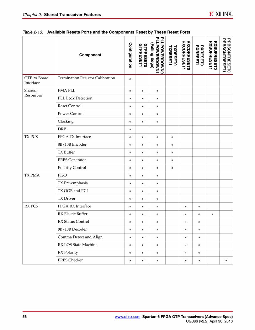
56 www.xilinx.com Spartan-6 FPGA GTP Transceivers (Advance Spec)UG386 (v2.2) April 30, 2010
Chapter 2: Shared Transceiver Features
Table 2-13: Available Resets Ports and the Components Reset by These Reset Ports
Component
Co
nfig
uratio
n
GT
PR
ES
ET
0G
TP
RE
SE
T1
PL
LP
OW
ER
DO
WN
0P
LL
PO
WE
RD
OW
N1
(Falling
Ed
ge)
TX
RE
SE
T0
TX
RE
SE
T1
RX
CD
RR
ES
ET
0R
XC
DR
RE
SE
T1
RX
RE
SE
T0
RX
RE
SE
T1
RX
BU
FR
ES
ET
0R
XB
UF
RE
SE
T1
PR
BS
CN
TR
ES
ET
0P
RB
SC
NT
RE
SE
T1
GTP-to-Board Interface
Termination Resistor Calibration *
Shared Resources
PMA PLL * * *
PLL Lock Detection * * *
Reset Control * * *
Power Control * * *
Clocking * * *
DRP *
TX PCS FPGA TX Interface * * * *
8B/10B Encoder * * * *
TX Buffer * * * *
PRBS Generator * * * *
Polarity Control * * * *
TX PMA PISO * * *
TX Pre-emphasis * * *
TX OOB and PCI * * *
TX Driver * * *
RX PCS FPGA RX Interface * * * * *
RX Elastic Buffer * * * * * *
RX Status Control * * * * *
8B/10B Decoder * * * * *
Comma Detect and Align * * * * *
RX LOS State Machine * * * * *
RX Polarity * * * * *
PRBS Checker * * * * * *
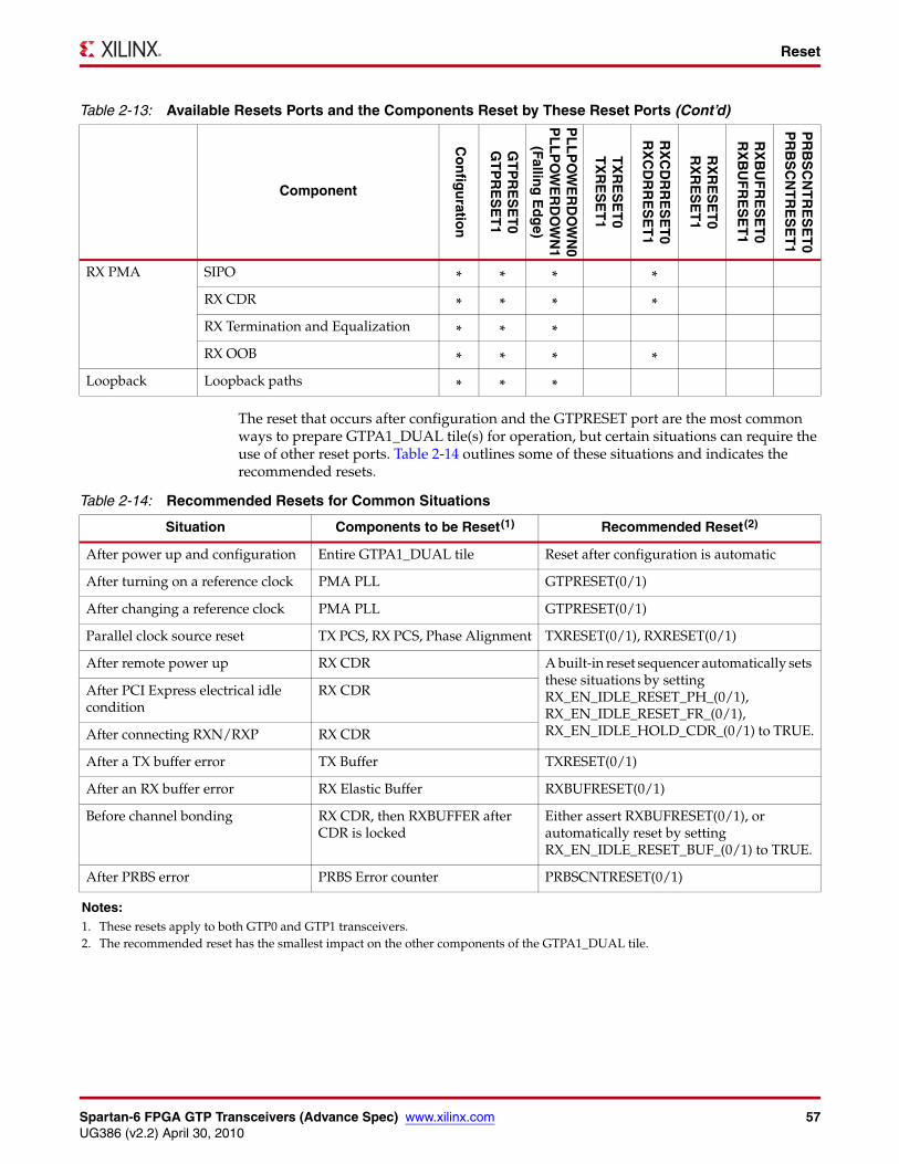
Spartan-6 FPGA GTP Transceivers (Advance Spec) www.xilinx.com 57UG386 (v2.2) April 30, 2010
Reset
The reset that occurs after configuration and the GTPRESET port are the most common ways to prepare GTPA1_DUAL tile(s) for operation, but certain situations can require the use of other reset ports. Table 2-14 outlines some of these situations and indicates the recommended resets.
RX PMA SIPO * * * *
RX CDR * * * *
RX Termination and Equalization * * *
RX OOB * * * *
Loopback Loopback paths * * *
Table 2-13: Available Resets Ports and the Components Reset by These Reset Ports (Cont’d)
Component
Co
nfig
uratio
n
GT
PR
ES
ET
0G
TP
RE
SE
T1
PL
LP
OW
ER
DO
WN
0P
LL
PO
WE
RD
OW
N1
(Falling
Ed
ge)
TX
RE
SE
T0
TX
RE
SE
T1
RX
CD
RR
ES
ET
0R
XC
DR
RE
SE
T1
RX
RE
SE
T0
RX
RE
SE
T1
RX
BU
FR
ES
ET
0R
XB
UF
RE
SE
T1
PR
BS
CN
TR
ES
ET
0P
RB
SC
NT
RE
SE
T1
Table 2-14: Recommended Resets for Common Situations
Situation Components to be Reset(1) Recommended Reset(2)
After power up and configuration Entire GTPA1_DUAL tile Reset after configuration is automatic
After turning on a reference clock PMA PLL GTPRESET(0/1)
After changing a reference clock PMA PLL GTPRESET(0/1)
Parallel clock source reset TX PCS, RX PCS, Phase Alignment TXRESET(0/1), RXRESET(0/1)
After remote power up RX CDR A built-in reset sequencer automatically sets these situations by setting RX_EN_IDLE_RESET_PH_(0/1), RX_EN_IDLE_RESET_FR_(0/1), RX_EN_IDLE_HOLD_CDR_(0/1) to TRUE.
After PCI Express electrical idle condition
RX CDR
After connecting RXN/RXP RX CDR
After a TX buffer error TX Buffer TXRESET(0/1)
After an RX buffer error RX Elastic Buffer RXBUFRESET(0/1)
Before channel bonding RX CDR, then RXBUFFER after CDR is locked
Either assert RXBUFRESET(0/1), or automatically reset by setting RX_EN_IDLE_RESET_BUF_(0/1) to TRUE.
After PRBS error PRBS Error counter PRBSCNTRESET(0/1)
Notes: 1. These resets apply to both GTP0 and GTP1 transceivers.2. The recommended reset has the smallest impact on the other components of the GTPA1_DUAL tile.
58 www.xilinx.com Spartan-6 FPGA GTP Transceivers (Advance Spec)UG386 (v2.2) April 30, 2010
Chapter 2: Shared Transceiver Features
Examples
Power-up and Configuration
All GTPA1_DUAL tiles are reset automatically after configuration. The supplies for the calibration resistor and calibration resistor reference must be powered up before configuration to ensure correct calibration of the termination impedance of all transceivers.
After Turning on a Reference Clock
The reference clock source(s) and the power to the GTPA1_DUAL tile must be available before configuring the FPGA. The reference clock must be stable before configuration especially when using PLL based clock sources (e.g., voltage controlled crystal oscillators). If the reference clock(s) or GTPA1_DUAL tile(s) are powered up after configuration, apply GTPRESET to allow the PMA PLL to lock.
After Changing a Reference Clock
Whenever the reference clock input to a GTPA1_DUAL tile is changed, the PMA PLL must be reset afterwards to ensure that it locks to the new frequency. The GTPRESET ports must be used for this purpose.
Parallel Clock Source Reset
The clocks driving TXUSRCLK, RXUSRCLK, TXUSRCLK2, and RXUSRCLK2 must be stable for correct operation. These clocks are often driven from a PLL or DCM in the FPGA to meet phase and frequency requirements. If the DCM or PLL loses lock, and begins producing incorrect output, TXRESET and RXRESET must be used to hold transceiver PCS in reset until the clock source is locked again.
If the TX or RX buffer is bypassed and phase alignment is in use, phase alignment must be performed again after the clock source relocks.
After Remote Power-up
If the remote source of incoming data is powered up after the GTP transceiver receiving its data is operating, the RX CDR must be reset to ensure a clean lock to the incoming data. By following the guidelines in Link Idle Reset Support, page 55, the electrical idle reset situation is automatically managed.
Electrical Idle Reset
When the differential voltage of the RX input to a GTP transceiver drops to OOB or electrical idle levels, the RX CDR can be pulled out of lock by the apparent sudden change in frequency. By following the guidelines in Link Idle Reset Support, page 55, the electrical idle reset situation is automatically managed.
After Connecting RXP/RXN
When the RX data to the GTP transceiver comes from a connector that can be plugged in and unplugged, the RX CDR must be reset when the data source is plugged in to ensure that it can lock to incoming data. By following the guidelines in Link Idle Reset Support, page 55, the electrical idle reset situation is automatically managed.
Spartan-6 FPGA GTP Transceivers (Advance Spec) www.xilinx.com 59UG386 (v2.2) April 30, 2010
Power Down
After a TX Buffer Error
When the TX buffer overflows or underflows, it must be reset using TXRESET to ensure correct behavior.
After an RX Buffer Error
After an RX buffer overflow or underflow, the RX elastic buffer must be reset using the RXBUFRESET port to ensure correct behavior.
Before Channel Bonding
For successful channel bonding, the RX elastic buffers of all the bonded transceivers must be written using the same recovered frequency, and read using the same RXUSRCLK frequency.
To provide the same RXUSRCLK frequency to all bonded transceivers, use a low skew clock buffer (for example, a BUFG) to drive all the RXUSRCLK ports from the same clock source. Bonding should not be attempted until the clock source is stable.
To provide the same recovered clock to all bonded transceivers:
• All of the TX data sources must be locked to the same reference clock.
• All of the bonded transceivers must have CDR lock to the incoming data.
The required reset for channel bonding is as follows:
• To automatically reset the CDR of all bonded transceivers, set RX_EN_IDLE_RESET_PH, RX_EN_IDLE_RESET_FR, and RX_EN_IDLE_HOLD_CDR to TRUE.
• Wait for CDR lock and bit alignment on all bonded transceivers.
• Either assert RXBUFRESET to all bonded transceivers, or automatically reset by setting RX_EN_IDLE_RESET_BUF = TRUE to enable the RXBUFRESET sequence.
• Attempt channel bonding.
See RX CDR in Chapter 4 for recommended methods of detecting CDR lock.
After a PRBS Error
To clear the RXPRBSERR signal after the PRBS error threshold is exceeded, assert PRBSCNTRESET.
Power Down
Functional DescriptionThe GTP transceiver supports a range of power-down modes. These modes support both generic power management capabilities as well as those defined in the PCI Express and SATA standards.
The GTP transceiver offers different levels of power control. Each channel in each direction can be powered down separately using TXPOWERDOWN and RXPOWERDOWN. Each PLLPOWERDOWN port directly affects the associated PLL that is selected by PLL_SOURCE attribute.
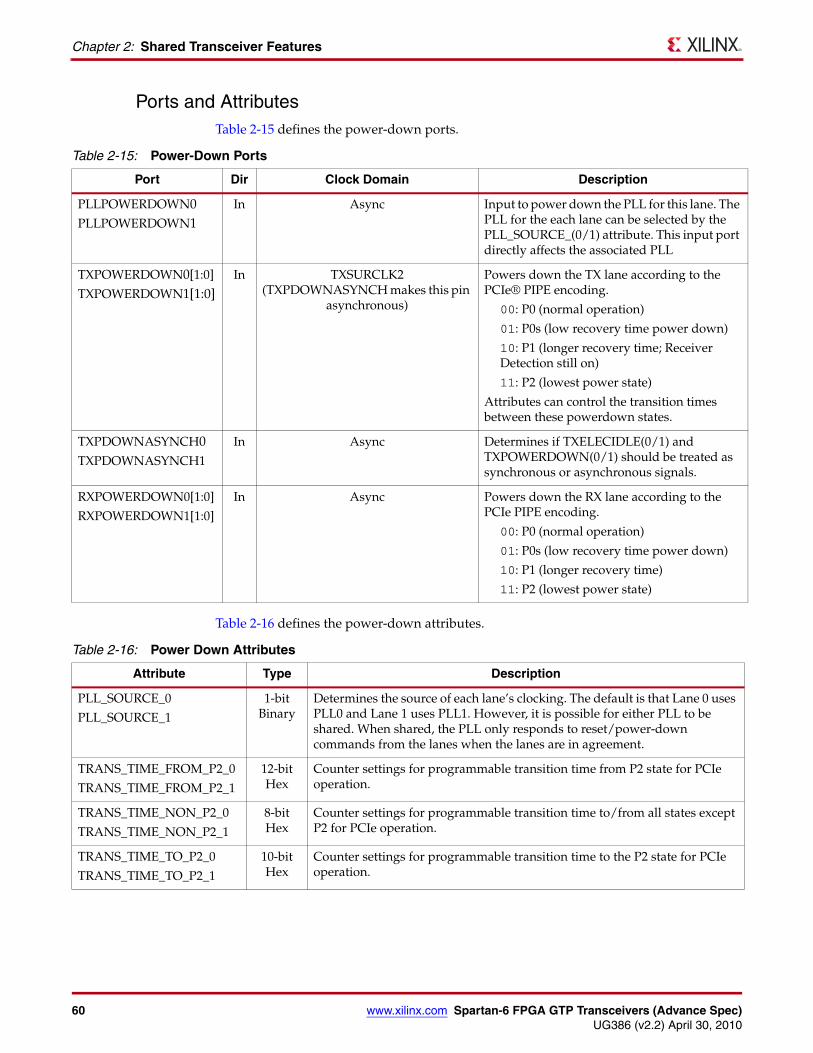
60 www.xilinx.com Spartan-6 FPGA GTP Transceivers (Advance Spec)UG386 (v2.2) April 30, 2010
Chapter 2: Shared Transceiver Features
Ports and AttributesTable 2-15 defines the power-down ports.
Table 2-16 defines the power-down attributes.
Table 2-15: Power-Down Ports
Port Dir Clock Domain Description
PLLPOWERDOWN0PLLPOWERDOWN1
In Async Input to power down the PLL for this lane. The PLL for the each lane can be selected by the PLL_SOURCE_(0/1) attribute. This input port directly affects the associated PLL
TXPOWERDOWN0[1:0]
TXPOWERDOWN1[1:0]In TXSURCLK2
(TXPDOWNASYNCH makes this pin asynchronous)
Powers down the TX lane according to the PCIe® PIPE encoding.
00: P0 (normal operation)
01: P0s (low recovery time power down)
10: P1 (longer recovery time; Receiver Detection still on)
11: P2 (lowest power state)
Attributes can control the transition times between these powerdown states.
TXPDOWNASYNCH0TXPDOWNASYNCH1
In Async Determines if TXELECIDLE(0/1) and TXPOWERDOWN(0/1) should be treated as synchronous or asynchronous signals.
RXPOWERDOWN0[1:0]
RXPOWERDOWN1[1:0]
In Async Powers down the RX lane according to the PCIe PIPE encoding.
00: P0 (normal operation)
01: P0s (low recovery time power down)
10: P1 (longer recovery time)
11: P2 (lowest power state)
Table 2-16: Power Down Attributes
Attribute Type Description
PLL_SOURCE_0
PLL_SOURCE_1
1-bit Binary
Determines the source of each lane’s clocking. The default is that Lane 0 uses PLL0 and Lane 1 uses PLL1. However, it is possible for either PLL to be shared. When shared, the PLL only responds to reset/power-down commands from the lanes when the lanes are in agreement.
TRANS_TIME_FROM_P2_0
TRANS_TIME_FROM_P2_1
12-bit Hex
Counter settings for programmable transition time from P2 state for PCIe operation.
TRANS_TIME_NON_P2_0
TRANS_TIME_NON_P2_1
8-bit Hex
Counter settings for programmable transition time to/from all states except P2 for PCIe operation.
TRANS_TIME_TO_P2_0
TRANS_TIME_TO_P2_1
10-bit Hex
Counter settings for programmable transition time to the P2 state for PCIe operation.
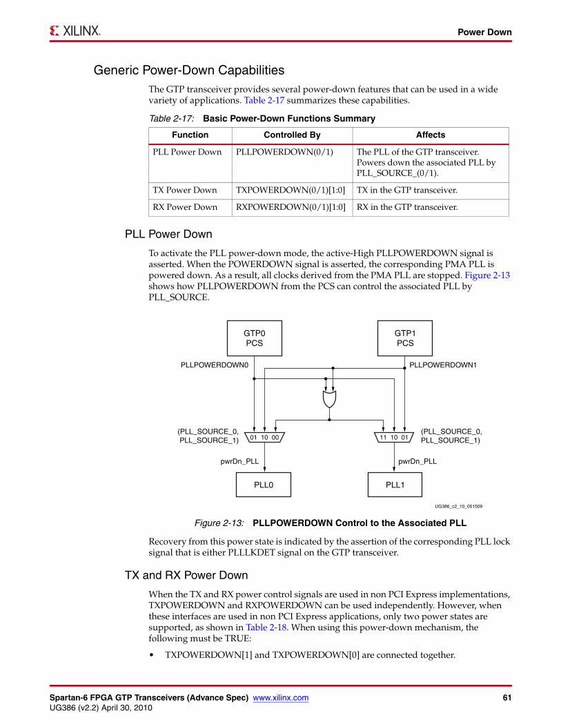
Spartan-6 FPGA GTP Transceivers (Advance Spec) www.xilinx.com 61UG386 (v2.2) April 30, 2010
Power Down
Generic Power-Down CapabilitiesThe GTP transceiver provides several power-down features that can be used in a wide variety of applications. Table 2-17 summarizes these capabilities.
PLL Power Down
To activate the PLL power-down mode, the active-High PLLPOWERDOWN signal is asserted. When the POWERDOWN signal is asserted, the corresponding PMA PLL is powered down. As a result, all clocks derived from the PMA PLL are stopped. Figure 2-13 shows how PLLPOWERDOWN from the PCS can control the associated PLL by PLL_SOURCE.
Recovery from this power state is indicated by the assertion of the corresponding PLL lock signal that is either PLLLKDET signal on the GTP transceiver.
TX and RX Power Down
When the TX and RX power control signals are used in non PCI Express implementations, TXPOWERDOWN and RXPOWERDOWN can be used independently. However, when these interfaces are used in non PCI Express applications, only two power states are supported, as shown in Table 2-18. When using this power-down mechanism, the following must be TRUE:
• TXPOWERDOWN[1] and TXPOWERDOWN[0] are connected together.
Table 2-17: Basic Power-Down Functions Summary
Function Controlled By Affects
PLL Power Down PLLPOWERDOWN(0/1) The PLL of the GTP transceiver. Powers down the associated PLL by PLL_SOURCE_(0/1).
TX Power Down TXPOWERDOWN(0/1)[1:0] TX in the GTP transceiver.
RX Power Down RXPOWERDOWN(0/1)[1:0] RX in the GTP transceiver.
X-Ref Target - Figure 2-13
Figure 2-13: PLLPOWERDOWN Control to the Associated PLL
01 10
GTP0PCS
PLL0
PLLPOWERDOWN1PLLPOWERDOWN0
(PLL_SOURCE_0,PLL_SOURCE_1)
(PLL_SOURCE_0,PLL_SOURCE_1)
pwrDn_PLLpwrDn_PLL
UG386_c2_10_051509
PLL1
GTP1PCS
00 11 10 01
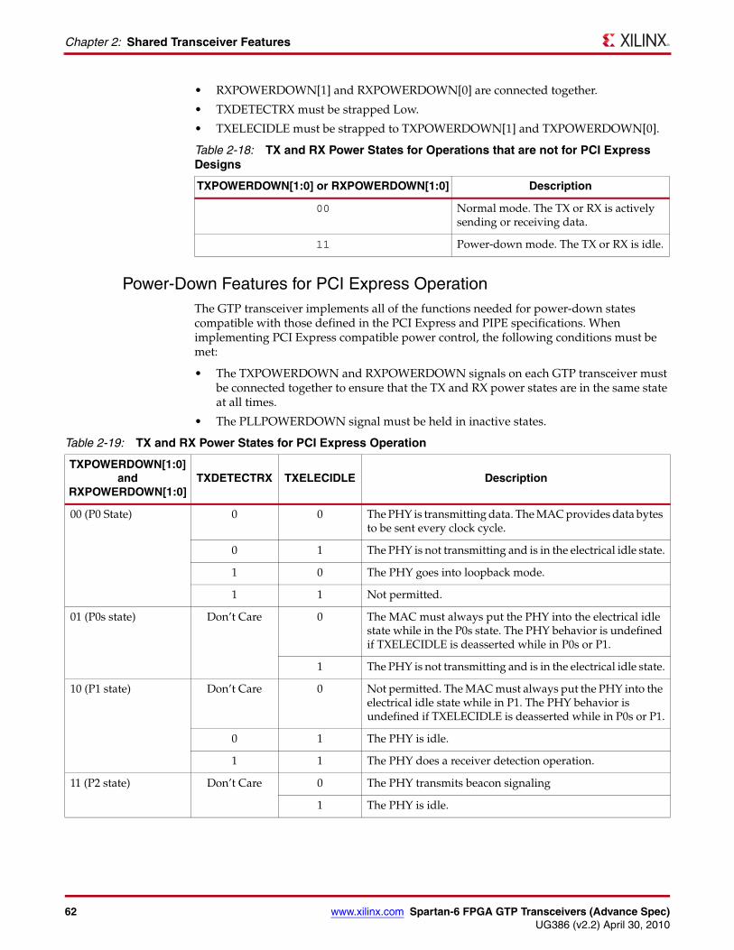
62 www.xilinx.com Spartan-6 FPGA GTP Transceivers (Advance Spec)UG386 (v2.2) April 30, 2010
Chapter 2: Shared Transceiver Features
• RXPOWERDOWN[1] and RXPOWERDOWN[0] are connected together.
• TXDETECTRX must be strapped Low.
• TXELECIDLE must be strapped to TXPOWERDOWN[1] and TXPOWERDOWN[0].
Power-Down Features for PCI Express OperationThe GTP transceiver implements all of the functions needed for power-down states compatible with those defined in the PCI Express and PIPE specifications. When implementing PCI Express compatible power control, the following conditions must be met:
• The TXPOWERDOWN and RXPOWERDOWN signals on each GTP transceiver must be connected together to ensure that the TX and RX power states are in the same state at all times.
• The PLLPOWERDOWN signal must be held in inactive states.
Table 2-18: TX and RX Power States for Operations that are not for PCI Express Designs
TXPOWERDOWN[1:0] or RXPOWERDOWN[1:0] Description
00 Normal mode. The TX or RX is actively sending or receiving data.
11 Power-down mode. The TX or RX is idle.
Table 2-19: TX and RX Power States for PCI Express Operation
TXPOWERDOWN[1:0] and
RXPOWERDOWN[1:0]TXDETECTRX TXELECIDLE Description
00 (P0 State) 0 0 The PHY is transmitting data. The MAC provides data bytes to be sent every clock cycle.
0 1 The PHY is not transmitting and is in the electrical idle state.
1 0 The PHY goes into loopback mode.
1 1 Not permitted.
01 (P0s state) Don’t Care 0 The MAC must always put the PHY into the electrical idle state while in the P0s state. The PHY behavior is undefined if TXELECIDLE is deasserted while in P0s or P1.
1 The PHY is not transmitting and is in the electrical idle state.
10 (P1 state) Don’t Care 0 Not permitted. The MAC must always put the PHY into the electrical idle state while in P1. The PHY behavior is undefined if TXELECIDLE is deasserted while in P0s or P1.
0 1 The PHY is idle.
1 1 The PHY does a receiver detection operation.
11 (P2 state) Don’t Care 0 The PHY transmits beacon signaling
1 The PHY is idle.
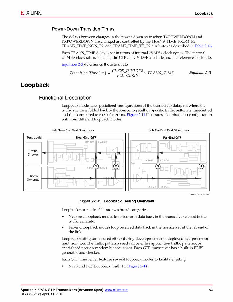
Spartan-6 FPGA GTP Transceivers (Advance Spec) www.xilinx.com 63UG386 (v2.2) April 30, 2010
Loopback
Power-Down Transition Times
The delays between changes in the power-down state when TXPOWERDOWN and RXPOWERDOWN are changed are controlled by the TRANS_TIME_FROM_P2, TRANS_TIME_NON_P2, and TRANS_TIME_TO_P2 attributes as described in Table 2-16.
Each TRANS_TIME delay is set in terms of internal 25 MHz clock cycles. The internal 25 MHz clock rate is set using the CLK25_DIVIDER attribute and the reference clock rate.
Equation 2-3 determines the actual rate.
Equation 2-3
Loopback
Functional DescriptionLoopback modes are specialized configurations of the transceiver datapath where the traffic stream is folded back to the source. Typically, a specific traffic pattern is transmitted and then compared to check for errors. Figure 2-14 illustrates a loopback test configuration with four different loopback modes.
Loopback test modes fall into two broad categories:
• Near-end loopback modes loop transmit data back in the transceiver closest to the traffic generator.
• Far-end loopback modes loop received data back in the transceiver at the far end of the link.
Loopback testing can be used either during development or in deployed equipment for fault isolation. The traffic patterns used can be either application traffic patterns, or specialized pseudo-random bit sequences. Each GTP transceiver has a built-in PRBS generator and checker.
Each GTP transceiver features several loopback modes to facilitate testing:
• Near-End PCS Loopback (path 1 in Figure 2-14)
Transition Time ns[ ] CLK25_DIVIDERPLL_CLKIN
------------------------------------------------- TRANS_TIME×=
X-Ref Target - Figure 2-14
Figure 2-14: Loopback Testing Overview
RX-PMARX-PCS
TX-PMATX-PCS
RX-PMA RX-PCS
TX-PMA TX-PCS
Near-End GTP
Link Near-End Test Structures Link Far-End Test Structures
Test Logic
UG386_c2_11_051509
Far-End GTP
TrafficChecker
TrafficGenerator
1 432
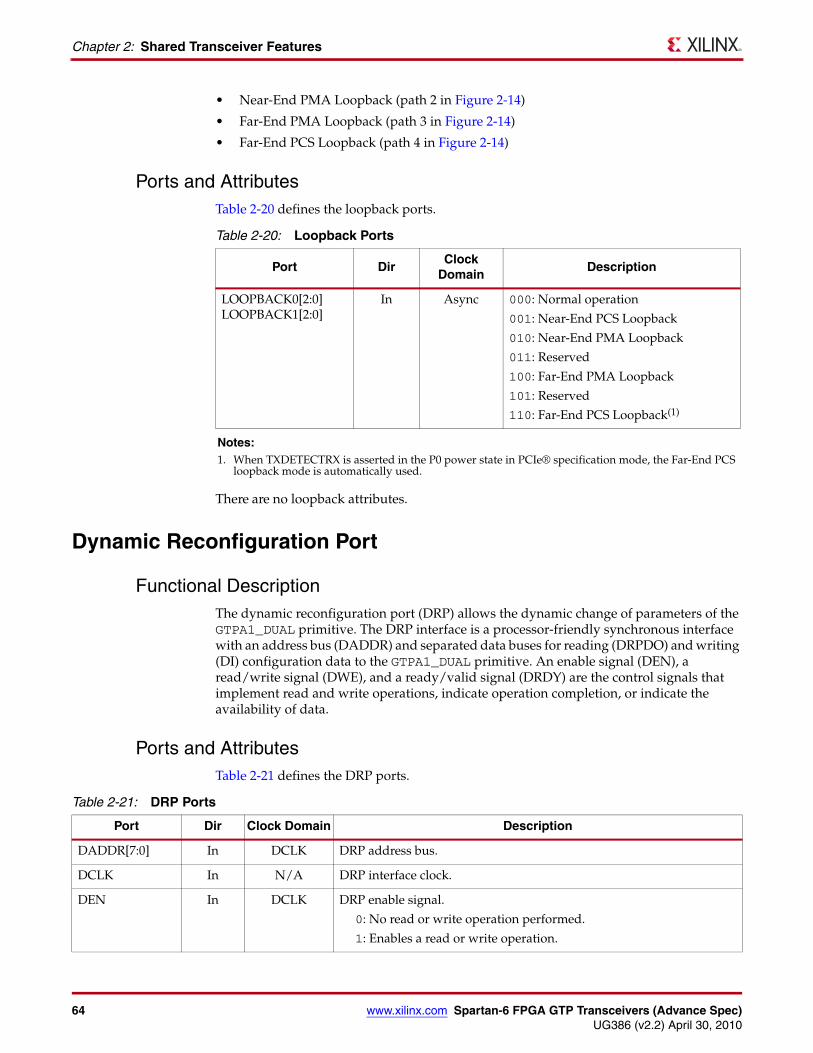
64 www.xilinx.com Spartan-6 FPGA GTP Transceivers (Advance Spec)UG386 (v2.2) April 30, 2010
Chapter 2: Shared Transceiver Features
• Near-End PMA Loopback (path 2 in Figure 2-14)
• Far-End PMA Loopback (path 3 in Figure 2-14)
• Far-End PCS Loopback (path 4 in Figure 2-14)
Ports and AttributesTable 2-20 defines the loopback ports.
There are no loopback attributes.
Dynamic Reconfiguration Port
Functional DescriptionThe dynamic reconfiguration port (DRP) allows the dynamic change of parameters of the GTPA1_DUAL primitive. The DRP interface is a processor-friendly synchronous interface with an address bus (DADDR) and separated data buses for reading (DRPDO) and writing (DI) configuration data to the GTPA1_DUAL primitive. An enable signal (DEN), a read/write signal (DWE), and a ready/valid signal (DRDY) are the control signals that implement read and write operations, indicate operation completion, or indicate the availability of data.
Ports and AttributesTable 2-21 defines the DRP ports.
Table 2-20: Loopback Ports
Port DirClock
DomainDescription
LOOPBACK0[2:0]LOOPBACK1[2:0]
In Async 000: Normal operation
001: Near-End PCS Loopback
010: Near-End PMA Loopback
011: Reserved
100: Far-End PMA Loopback
101: Reserved
110: Far-End PCS Loopback(1)
Notes: 1. When TXDETECTRX is asserted in the P0 power state in PCIe® specification mode, the Far-End PCS
loopback mode is automatically used.
Table 2-21: DRP Ports
Port Dir Clock Domain Description
DADDR[7:0] In DCLK DRP address bus.
DCLK In N/A DRP interface clock.
DEN In DCLK DRP enable signal.
0: No read or write operation performed.
1: Enables a read or write operation.
Spartan-6 FPGA GTP Transceivers (Advance Spec) www.xilinx.com 65UG386 (v2.2) April 30, 2010
Dynamic Reconfiguration Port
There are no DRP attributes.
DI[15:0] In DCLK Data bus for writing configuration data from the FPGA logic resources to the GTP transceiver.
DRPDO[15:0] Out DCLK Data bus for reading configuration data from the GTP transceiver to the FPGA logic resources.
DRDY Out DCLK Indicates operation is complete for write operations and data is valid for read operations.
DWE In DCLK DRP write enable.
0: Read operation when DEN is 1.
1: Write operation when DEN is 1.
Table 2-21: DRP Ports (Cont’d)
Port Dir Clock Domain Description

66 www.xilinx.com Spartan-6 FPGA GTP Transceivers (Advance Spec)UG386 (v2.2) April 30, 2010
Chapter 2: Shared Transceiver Features
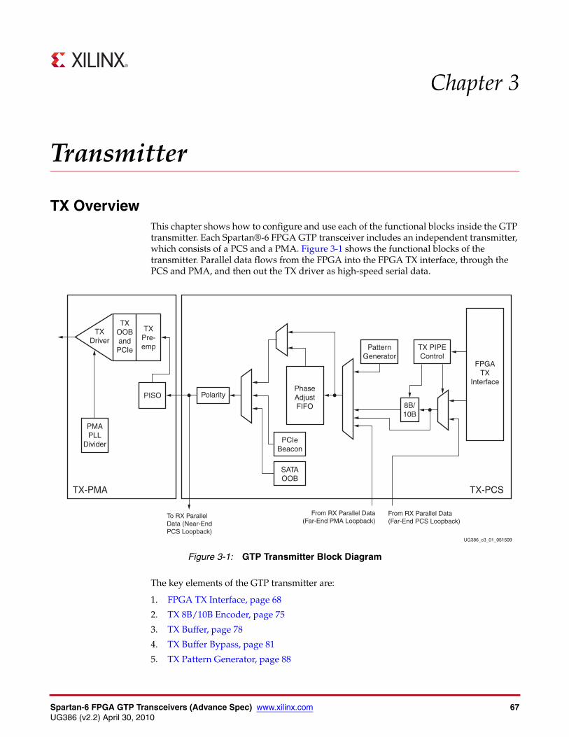
Spartan-6 FPGA GTP Transceivers (Advance Spec) www.xilinx.com 67UG386 (v2.2) April 30, 2010
Chapter 3
Transmitter
TX OverviewThis chapter shows how to configure and use each of the functional blocks inside the GTP transmitter. Each Spartan®-6 FPGA GTP transceiver includes an independent transmitter, which consists of a PCS and a PMA. Figure 3-1 shows the functional blocks of the transmitter. Parallel data flows from the FPGA into the FPGA TX interface, through the PCS and PMA, and then out the TX driver as high-speed serial data.
The key elements of the GTP transmitter are:
1. FPGA TX Interface, page 68
2. TX 8B/10B Encoder, page 75
3. TX Buffer, page 78
4. TX Buffer Bypass, page 81
5. TX Pattern Generator, page 88
X-Ref Target - Figure 3-1
Figure 3-1: GTP Transmitter Block Diagram
TX-PMA TX-PCS
FPGATX
Interface
UG386_c3_01_051509
TX PIPEControl
PhaseAdjustFIFO
PCIeBeacon
From RX Parallel Data(Far-End PMA Loopback)
To RX ParallelData (Near-End PCS Loopback)
From RX Parallel Data(Far-End PCS Loopback)
PISO
TXPre-emp
PMAPLL
Divider
TXOOBandPCIe
TXDriver
Polarity
SATAOOB
8B/10B
PatternGenerator
68 www.xilinx.com Spartan-6 FPGA GTP Transceivers (Advance Spec)UG386 (v2.2) April 30, 2010
Chapter 3: Transmitter
6. TX Polarity Control, page 91
7. TX Fabric Clock Output Control, page 91
8. TX Configurable Driver, page 94
9. TX Receiver Detect Support for PCI Express Designs, page 97
10. TX Out-of-Band Signaling, page 99
FPGA TX Interface
Functional DescriptionThe FPGA TX interface is the FPGA’s gateway to the TX datapath of the GTP transceiver. Applications transmit data through the GTP transceiver by writing data to the TXDATA port on the positive edge of TXUSRCLK2.
The width of the port can be configured to be one, two, or four bytes wide. The actual width of the port depends on the GTPA1_DUAL tile’s INTDATAWIDTH setting (controls the width of the internal datapath), and whether or not the 8B/10B encoder is enabled. Port widths can be 8, 10, 16, 20, 32, and 40 bits.
The rate of the parallel clock (TXUSRCLK2) at the interface is determined by the TX line rate, the width of the TXDATA port, and whether or not 8B/10B encoding is enabled. A second parallel clock (TXUSRCLK) must be provided for the internal PCS logic in the transmitter. This section shows how to drive the parallel clocks and explains the constraints on those clocks for correct operation. The highest transmitter data rates require a 4-byte interface to achieve a TXUSRCLK2 rate in the specified operating range.
Ports and AttributesTable 3-1 defines the FPGA TX Interface ports.
Table 3-1: FPGA TX Interface Ports
Port Direction Clock Domain Description
INTDATAWIDTH0INTDATAWIDTH1
In Async
Specifies the width of the internal datapath for each GTP transceiver.
• 0: Internal datapath is 8 bits wide• 1: Internal datapath is 10 bits wide
Note: If the PLL is shared between both GTP transceivers, then INTDATAWIDTH0 must equal INTDATAWIDTH1.
GTPCLKOUT0[1:0]
GTPCLKOUT1[1:0]Out N/A
The GTPCLKOUT(0/1) ports from each GTPA1_DUAL tile provides direct access to the reference clock provided to the shared PMA PLL (CLKIN). GTPCLKOUT(0/1) can be routed for use in the FPGA logic via a BUFIO2 primitive.
Spartan-6 FPGA GTP Transceivers (Advance Spec) www.xilinx.com 69UG386 (v2.2) April 30, 2010
FPGA TX Interface
TXCHARDISPMODE0[3:0]
TXCHARDISPMODE1[3:0]In TXUSRCLK2
TXCHARDISPMODE and TXCHARDISPVAL allow control of the 8B/10B outgoing data disparity when 8B/10B encoding is enabled.
When 8B/10B encoding is disabled, TXCHARDISPMODE is used to extend the data bus for TX interfaces with a width that is a multiple of 10.
TXCHARDISPMODE[3] corresponds to TXDATA[31:24]
TXCHARDISPMODE[2] corresponds to TXDATA[23:16]
TXCHARDISPMODE[1] corresponds to TXDATA[15:8]
TXCHARDISPMODE[0] corresponds to TXDATA[7:0]
Table 3-3, page 77 shows how to use TXCHARDISPMODE to control the disparity of outgoing data when 8B/10B encoding is enabled.
TXCHARDISPVAL0[3:0]
TXCHARDISPVAL1[3:0]In TXUSRCLK2
TXCHARDISPVAL and TXCHARDISPMODE allow control of the 8B/10B outgoing data disparity when 8B/10B encoding is enabled.
When 8B/10B encoding is disabled, TXCHARDISPVAL is used to extend the data bus for 10-, 20-, and 40-bit TX interfaces.
TXCHARDISPVAL[3] corresponds to TXDATA[31:24]
TXCHARDISPVAL[2] corresponds to TXDATA[23:16]
TXCHARDISPVAL[1] corresponds to TXDATA[15:8]
TXCHARDISPVAL[0] corresponds to TXDATA[7:0]
Table 3-3, page 77 shows how to use TXCHARDISPVAL to control the disparity of outgoing data when 8B/10B encoding is enabled.
TXDATA0[31:0]
TXDATA1[31:0]In TXUSRCLK2
TXDATA is the bus for transmitting data. The width of this port depends on TXDATAWIDTH:
• TXDATAWIDTH = 0: TXDATA[7:0] = 8 bits wide• TXDATAWIDTH = 1: TXDATA[15:0] = 16 bits wide• TXDATAWIDTH = 2: TXDATA[31:0] = 32 bits wide
When a 10-bit, 20-bit, or 40-bit bus is required, the TXCHARDISPVAL and TXCHARDISPMODE ports from the 8B/10B encoder are concatenated with the TXDATA port.
TXDATAWIDTH0[1:0]
TXDATAWIDTH1[1:0]In TXUSRCLK2
Selects the width of the TXDATA port.
• 0: TXDATA is 8 bits or 10 bits wide• 1: TXDATA is 16 bits or 20 bits wide• 2: TXDATA is 32 bits or 40 bits wide• 3: Reserved
TXENC8B10BUSE0
TXENC8B10BUSE1In TXUSRCLK2
TXENC8B10BUSE is set High to enable the 8B/10B encoder. INTDATAWIDTH(0/1) must also be High.
0: 8B/10B encoder bypassed. This option reduces latency.
1: 8B/10B encoder enabled. INTDATAWIDTH(0/1) must be High.
Table 3-1: FPGA TX Interface Ports (Cont’d)
Port Direction Clock Domain Description
70 www.xilinx.com Spartan-6 FPGA GTP Transceivers (Advance Spec)UG386 (v2.2) April 30, 2010
Chapter 3: Transmitter
There are no FPGA TX Interface attributes.
DescriptionThe FPGA TX interface allows parallel data to be written to the GTP transceiver for transmission as serial data. To use the interface:
• The width of the data interface must be configured
• TXUSRCLK2 and TXUSRCLK must be connected to clocks running at the correct rate
Configuring the Width of the Interface
Table 3-2 shows how the interface width for the TX datapath is selected. 8B/10B encoding is discussed in more detail in TX 8B/10B Encoder, page 75.
TXOUTCLK0
TXOUTCLK1Out N/A
This port provides a parallel clock generated by the GTP transceiver. This clock can be used to drive TXUSRCLK for one or more GTP transceivers. The rate of the clock depends on INTDATAWIDTH(0/1):
• INTDATAWIDTH(0/1) is Low: FTXOUTCLK(0/1) = Line Rate/8
• INTDATAWIDTH(0/1) is High: FTXOUTCLK(0/1) = Line Rate/10
TXRESET0
TXRESET1In Async
Resets the PCS of the GTP transmitter, including the phase adjust FIFO, the 8B/10B encoder, and the FPGA TX interface.
TXUSRCLK0(1)
TXUSRCLK1In N/A
This port is used to provide a clock for the internal TX PCS datapath. This clock must always be provided. The rate depends on INTDATAWIDTH(0/1):
• INTDATAWIDTH(0/1) is Low: FTXUSRCLK(0/1) = Line Rate/8
• INTDATAWIDTH(0/1) is High: FTXUSRCLK(0/1) = Line Rate/10
TXUSRCLK20(1)
TXUSRCLK21In N/A
This port is used to synchronize the FPGA logic with the TX interface. This clock must be positive-edge aligned to TXUSRCLK. The rate of this clock depends on FTXUSRCLK and TXDATAWIDTH:
• TXDATAWIDTH = 0: FTXUSRCLK2 = FTXUSRCLK• TXDATAWIDTH = 1: FTXUSRCLK2 = FTXUSRCLK/2• TXDATAWIDTH = 2: FTXUSRCLK2 = FTXUSRCLK/4
Notes: 1. Refer to the Spartan-6 FGPA Data Sheet for the frequency specification of TXUSRCLK and TXUSRCLK2.
Table 3-1: FPGA TX Interface Ports (Cont’d)
Port Direction Clock Domain Description
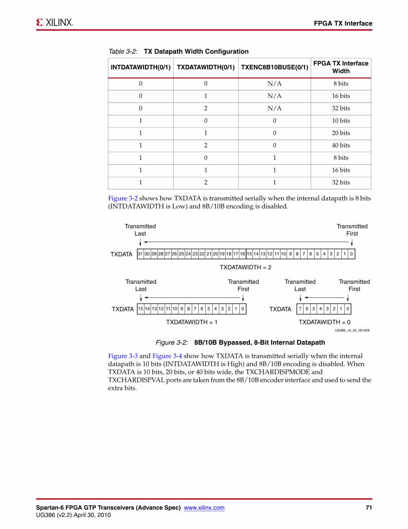
Spartan-6 FPGA GTP Transceivers (Advance Spec) www.xilinx.com 71UG386 (v2.2) April 30, 2010
FPGA TX Interface
Figure 3-2 shows how TXDATA is transmitted serially when the internal datapath is 8 bits (INTDATAWIDTH is Low) and 8B/10B encoding is disabled.
Figure 3-3 and Figure 3-4 show how TXDATA is transmitted serially when the internal datapath is 10 bits (INTDATAWIDTH is High) and 8B/10B encoding is disabled. When TXDATA is 10 bits, 20 bits, or 40 bits wide, the TXCHARDISPMODE and TXCHARDISPVAL ports are taken from the 8B/10B encoder interface and used to send the extra bits.
Table 3-2: TX Datapath Width Configuration
INTDATAWIDTH(0/1) TXDATAWIDTH(0/1) TXENC8B10BUSE(0/1)FPGA TX Interface
Width
0 0 N/A 8 bits
0 1 N/A 16 bits
0 2 N/A 32 bits
1 0 0 10 bits
1 1 0 20 bits
1 2 0 40 bits
1 0 1 8 bits
1 1 1 16 bits
1 2 1 32 bits
X-Ref Target - Figure 3-2
Figure 3-2: 8B/10B Bypassed, 8-Bit Internal Datapath
UG386_c3_02_051409
15 14 13 12 11 10 9 8 7 6 5 4 3 2 1 0 7 6 5 4 3 2 1 0
TransmittedLast
TransmittedLast
TransmittedFirst
TransmittedLast
TransmittedFirst
TransmittedFirst
TXDATA
TXDATAWIDTH = 0
TXDATAWIDTH = 2
TXDATAWIDTH = 1
TXDATA
15 14 13 12 11 10 9 8 7 6 5 4 3 2 1 031 30 29 28 27 26 25 24 23 22 21 20 19 18 17 16TXDATA
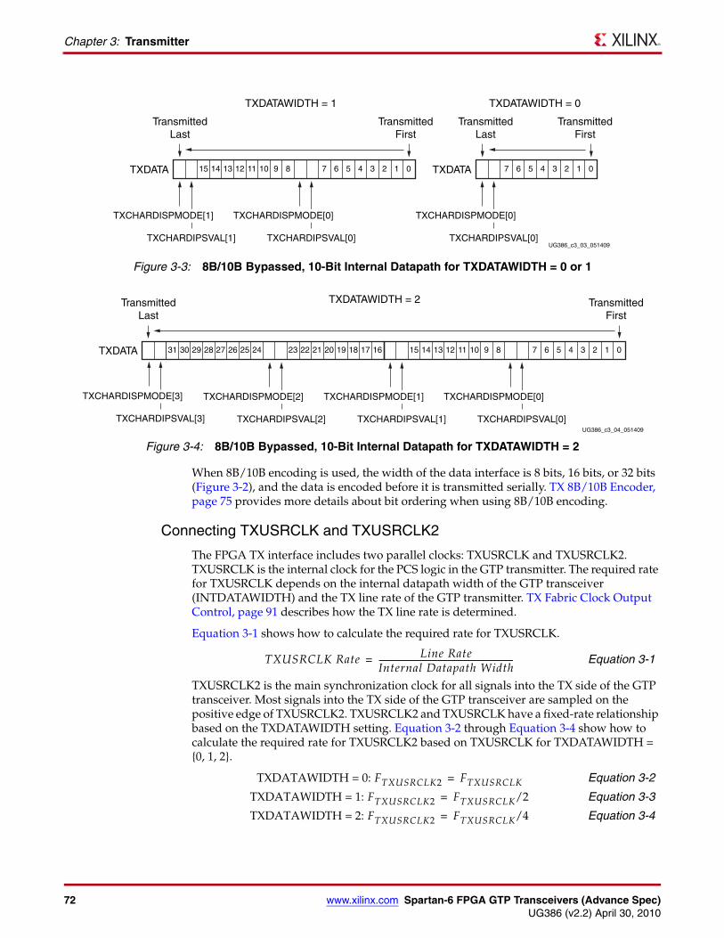
72 www.xilinx.com Spartan-6 FPGA GTP Transceivers (Advance Spec)UG386 (v2.2) April 30, 2010
Chapter 3: Transmitter
When 8B/10B encoding is used, the width of the data interface is 8 bits, 16 bits, or 32 bits (Figure 3-2), and the data is encoded before it is transmitted serially. TX 8B/10B Encoder, page 75 provides more details about bit ordering when using 8B/10B encoding.
Connecting TXUSRCLK and TXUSRCLK2
The FPGA TX interface includes two parallel clocks: TXUSRCLK and TXUSRCLK2. TXUSRCLK is the internal clock for the PCS logic in the GTP transmitter. The required rate for TXUSRCLK depends on the internal datapath width of the GTP transceiver (INTDATAWIDTH) and the TX line rate of the GTP transmitter. TX Fabric Clock Output Control, page 91 describes how the TX line rate is determined.
Equation 3-1 shows how to calculate the required rate for TXUSRCLK.
Equation 3-1
TXUSRCLK2 is the main synchronization clock for all signals into the TX side of the GTP transceiver. Most signals into the TX side of the GTP transceiver are sampled on the positive edge of TXUSRCLK2. TXUSRCLK2 and TXUSRCLK have a fixed-rate relationship based on the TXDATAWIDTH setting. Equation 3-2 through Equation 3-4 show how to calculate the required rate for TXUSRCLK2 based on TXUSRCLK for TXDATAWIDTH = {0, 1, 2}.
Equation 3-2
Equation 3-3
Equation 3-4
X-Ref Target - Figure 3-3
Figure 3-3: 8B/10B Bypassed, 10-Bit Internal Datapath for TXDATAWIDTH = 0 or 1
X-Ref Target - Figure 3-4
Figure 3-4: 8B/10B Bypassed, 10-Bit Internal Datapath for TXDATAWIDTH = 2
TXDATA15 14 13 12 11 10 9 8 7 6 5 4 3 2 1 0 7 6 5 4 3 2 1 0
UG386_c3_03_051409
TransmittedLast
TransmittedLast
TransmittedFirst
TransmittedFirst
TXDATA
TXDATAWIDTH = 1 TXDATAWIDTH = 0
TXCHARDISPMODE[1]
TXCHARDIPSVAL[1]
TXCHARDISPMODE[0]
TXCHARDIPSVAL[0]
TXCHARDISPMODE[0]
TXCHARDIPSVAL[0]
15 14 13 12 11 10 9 8 7 6 5 4 3 2 1 023 22 21 161718192031 30 29 2425262728
UG386_c3_04_051409
TransmittedLast
TransmittedFirst
TXDATA
TXDATAWIDTH = 2
TXCHARDISPMODE[1]
TXCHARDIPSVAL[1]
TXCHARDISPMODE[2]
TXCHARDIPSVAL[2]TXCHARDIPSVAL[3]
TXCHARDISPMODE[3] TXCHARDISPMODE[0]
TXCHARDIPSVAL[0]
TXUSRCLK Rate Line RateInternal Datapath Width--------------------------------------------------------------------=
TXDATAWIDTH = 0: FTXUSRCLK2 FTXUSRCLK=
TXDATAWIDTH = 1: FTXUSRCLK2 FTXUSRCLK/2=
TXDATAWIDTH = 2: FTXUSRCLK2 FTXUSRCLK/4=
Spartan-6 FPGA GTP Transceivers (Advance Spec) www.xilinx.com 73UG386 (v2.2) April 30, 2010
FPGA TX Interface
The following rules about the relationships between clocks must be observed for TXUSRCLK, TXUSRCLK2, and CLKIN (reference clock provided to the PMA PLL):
• TXUSRCLK and TXUSRCLK2 must be positive-edge aligned with as little skew as possible between them. As a result, low-skew clock resources (BUFGs) should be used to drive TXUSRCLK and TXUSRCLK2. When TXUSRCLK and TXUSRCLK2 have the same frequency, the same clock resource is used to drive both. When the two clocks have different frequencies, TXUSRCLK is used to derive TXUSRCLK2 through the division of TXUSRCLK. The designer must ensure that the two clocks are positive-edge aligned.
• Even though they might run at different frequencies, TXUSRCLK, TXUSRCLK2, and CLKIN must have the same oscillator as their source. Thus TXUSRCLK and TXUSRCLK2 must be multiplied or divided versions of CLKIN. The GTP transceiver provides access to CLKIN in two ways: the GTPCLKOUT ports and the TXOUTCLK port.
• GTPCLKOUT0[1:0] is for lane 0 and GTPCLKOUT1[1:0] is for lane 1 within a single GTPA1_DUAL. GTPCLKOUT0 and GTPCLKOUT1 must be connected to their dedicated BUFIO2 resources before they can be used by the fabric resources (BUFG, PLL, or DCM).
• GTPCLKOUT[1] is the recovered clock from the CDR unit.
• GTPCLKOUT[0] can be sourced by TXOUTCLK or REFCLKPLL by using the CLK_OUT_GTP_SEL attribute setting. The user is recommended to use the GTPCLKOUT[0] port and select the appropriate attribute setting.
• REFCLKPLL is a free-running clock if it is driven by a stable clock source via the reference clock multiplexer structure. It operates even before the shared PMA PLL is locked. However, because GTPCLKOUT[0] uses the CLKIN rate, the generation of TXUSRCLK or TXUSRCLK2 can require multiplication or division to produce the required rates.
• TXOUTCLK sourcing GTPCLKOUT[0] provides a copy of CLKIN already divided to the TXUSRCLK rate, potentially requiring fewer dividers. However, TXOUTCLK is not free-running. It is only valid after the shared PMA PLL is locked and cannot be used when TX phase alignment is turned on.
• In use models where the TX buffer or RX buffer is bypassed, the user should refer to TX Buffer Bypass, page 81 or RX Elastic Buffer Bypass, page 133 for more information.
Using GTPCLKOUT to Drive the GTP TXFigure 3-5 through Figure 3-7 show different ways in which the FPGA clock resources can be used to drive the parallel clocks for the TX interface. The GTPCLKOUT ports are connected to specific BUFIO2 primitives to access the DCM/PLL/BUFG clock resources. This can affect global clock pins located in bank 0 or bank 2. Refer to the Spartan-6 FPGA Clocking Resources User Guide for more information.
GTPCLKOUT Driving a GTP TX in 1-Byte Mode
In Figure 3-5, GTPCLKOUT[0] is used to drive TXUSRCLK and TXUSRCLK2 for 1-byte mode (TXDATAWIDTH = 00 and INTDATAWIDTH = 0 or 1). Because TXUSRCLK and TXUSRCLK2 have the same rate, the output of the BUFG can be connected to both TXUSRCLK and TXUSRCLK2.
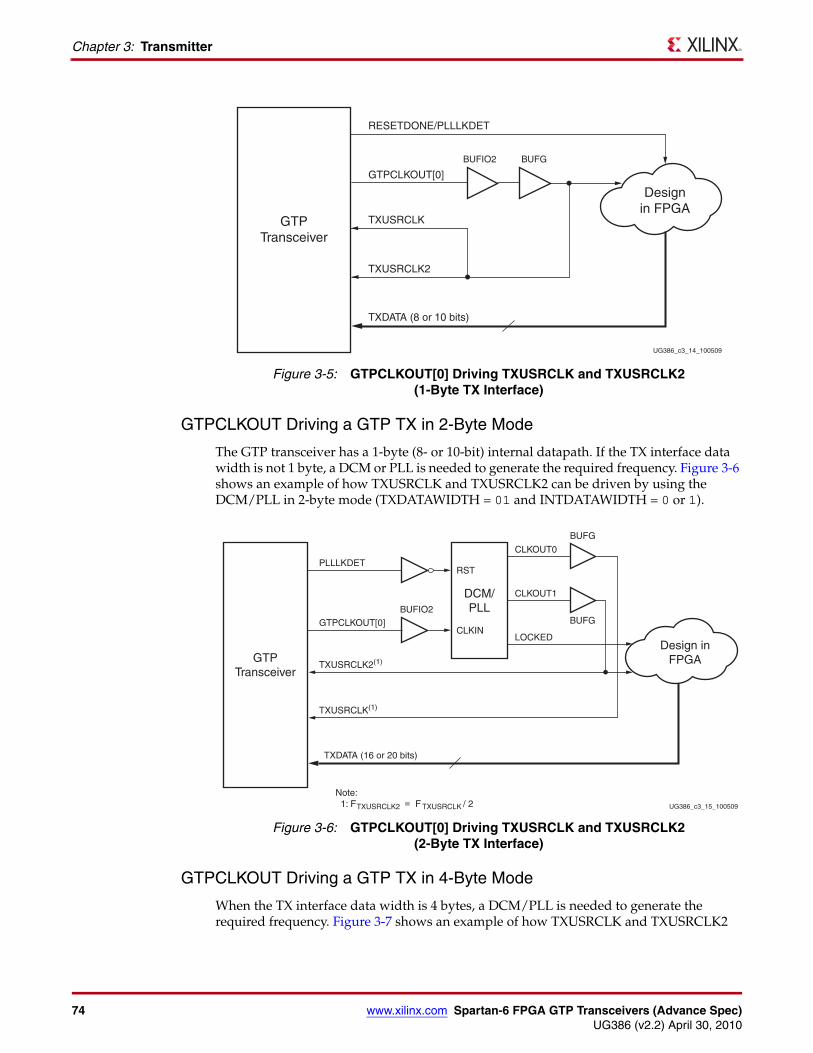
74 www.xilinx.com Spartan-6 FPGA GTP Transceivers (Advance Spec)UG386 (v2.2) April 30, 2010
Chapter 3: Transmitter
GTPCLKOUT Driving a GTP TX in 2-Byte Mode
The GTP transceiver has a 1-byte (8- or 10-bit) internal datapath. If the TX interface data width is not 1 byte, a DCM or PLL is needed to generate the required frequency. Figure 3-6 shows an example of how TXUSRCLK and TXUSRCLK2 can be driven by using the DCM/PLL in 2-byte mode (TXDATAWIDTH = 01 and INTDATAWIDTH = 0 or 1).
GTPCLKOUT Driving a GTP TX in 4-Byte Mode
When the TX interface data width is 4 bytes, a DCM/PLL is needed to generate the required frequency. Figure 3-7 shows an example of how TXUSRCLK and TXUSRCLK2
X-Ref Target - Figure 3-5
Figure 3-5: GTPCLKOUT[0] Driving TXUSRCLK and TXUSRCLK2(1-Byte TX Interface)
UG386_c3_14_100509
BUFIO2 BUFG
GTPCLKOUT[0]
TXUSRCLK
TXUSRCLK2
TXDATA (8 or 10 bits)
RESETDONE/PLLLKDET
Designin FPGA
GTPTransceiver
X-Ref Target - Figure 3-6
Figure 3-6: GTPCLKOUT[0] Driving TXUSRCLK and TXUSRCLK2(2-Byte TX Interface)
UG386_c3_15_100509
BUFIO2GTPCLKOUT[0]
TXUSRCLK2(1)
TXUSRCLK(1)
TXDATA (16 or 20 bits)
PLLLKDETCLKOUT0
TXUSRCLK2
Note: 1: F TXUSRCLK
F
/ 2=
CLKOUT1
LOCKED
RST
CLKIN
Design inFPGA
DCM/PLL
GTPTransceiver
BUFG
BUFG
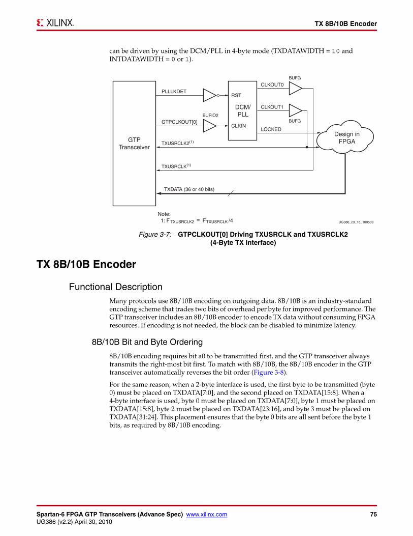
Spartan-6 FPGA GTP Transceivers (Advance Spec) www.xilinx.com 75UG386 (v2.2) April 30, 2010
TX 8B/10B Encoder
can be driven by using the DCM/PLL in 4-byte mode (TXDATAWIDTH = 10 and INTDATAWIDTH = 0 or 1).
TX 8B/10B Encoder
Functional DescriptionMany protocols use 8B/10B encoding on outgoing data. 8B/10B is an industry-standard encoding scheme that trades two bits of overhead per byte for improved performance. The GTP transceiver includes an 8B/10B encoder to encode TX data without consuming FPGA resources. If encoding is not needed, the block can be disabled to minimize latency.
8B/10B Bit and Byte Ordering
8B/10B encoding requires bit a0 to be transmitted first, and the GTP transceiver always transmits the right-most bit first. To match with 8B/10B, the 8B/10B encoder in the GTP transceiver automatically reverses the bit order (Figure 3-8).
For the same reason, when a 2-byte interface is used, the first byte to be transmitted (byte 0) must be placed on TXDATA[7:0], and the second placed on TXDATA[15:8]. When a 4-byte interface is used, byte 0 must be placed on TXDATA[7:0], byte 1 must be placed on TXDATA[15:8], byte 2 must be placed on TXDATA[23:16], and byte 3 must be placed on TXDATA[31:24]. This placement ensures that the byte 0 bits are all sent before the byte 1 bits, as required by 8B/10B encoding.
X-Ref Target - Figure 3-7
Figure 3-7: GTPCLKOUT[0] Driving TXUSRCLK and TXUSRCLK2(4-Byte TX Interface)
UG386_c3_16_100509
BUFIO2
GTPCLKOUT[0]
TXUSRCLK2(1)
TXUSRCLK(1)
TXDATA (36 or 40 bits)
PLLLKDETCLKOUT0
TXUSRCLK2
Note: 1: F TXUSRCLK
F
/4=
CLKOUT1
LOCKED
RST
CLKIN
DCM/PLL
GTPTransceiver
BUFG
BUFG
Design inFPGA
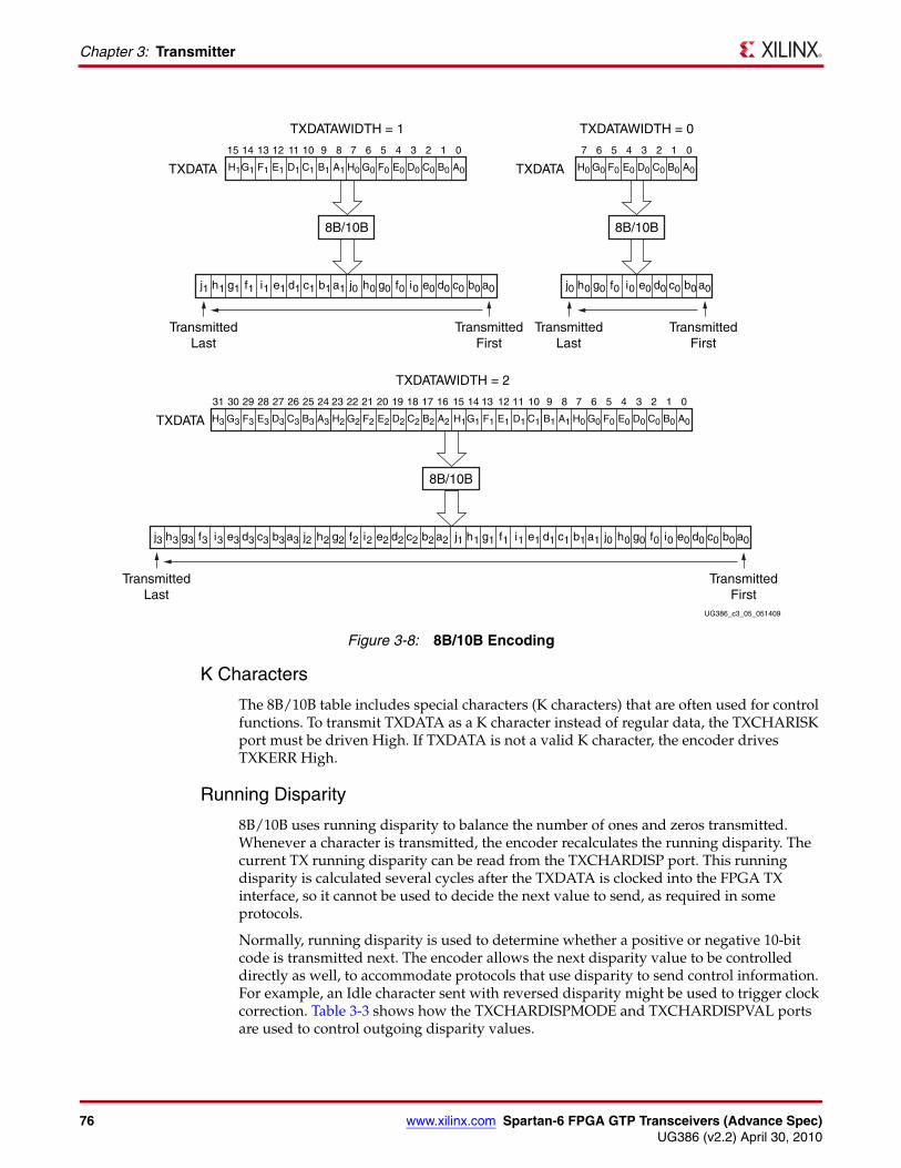
76 www.xilinx.com Spartan-6 FPGA GTP Transceivers (Advance Spec)UG386 (v2.2) April 30, 2010
Chapter 3: Transmitter
K Characters
The 8B/10B table includes special characters (K characters) that are often used for control functions. To transmit TXDATA as a K character instead of regular data, the TXCHARISK port must be driven High. If TXDATA is not a valid K character, the encoder drives TXKERR High.
Running Disparity
8B/10B uses running disparity to balance the number of ones and zeros transmitted. Whenever a character is transmitted, the encoder recalculates the running disparity. The current TX running disparity can be read from the TXCHARDISP port. This running disparity is calculated several cycles after the TXDATA is clocked into the FPGA TX interface, so it cannot be used to decide the next value to send, as required in some protocols.
Normally, running disparity is used to determine whether a positive or negative 10-bit code is transmitted next. The encoder allows the next disparity value to be controlled directly as well, to accommodate protocols that use disparity to send control information. For example, an Idle character sent with reversed disparity might be used to trigger clock correction. Table 3-3 shows how the TXCHARDISPMODE and TXCHARDISPVAL ports are used to control outgoing disparity values.
X-Ref Target - Figure 3-8
Figure 3-8: 8B/10B Encoding
TransmittedLast
a0b0c0d0e0i0f0g0h0j0
a0b0c0d0e0i0f0g0h0j0a1b1c1d1e1i1f1g1h1j1a2b2c2d2e2i2f2g2h2j2a3b3c3d3e3i3f3g3h3j3
UG386_c3_05_051409
TXDATA
TXDATAWIDTH = 2
8B/10B
15 14 13 12 11 10 9 8 7 6 5 4 3 2 1 0
H1G1 F1 E1 D1 C1 B1 A1 H0 G0 F0 E0 D0 C0 B0 A0
H0 G0 F0 E0 D0 C0 B0 A0
7 6 5 4 3 2 1 0
H3 G3 F3 E3 D3 C3 B3 A3TXDATA H2 G2 F2 E2 D2 C2 B2 A2
23 22 21 20 19 18 17 1631 30 29 28 27 26 25 24
8B/10B
TXDATAWIDTH = 0
TransmittedLast
TransmittedFirst
TransmittedFirst
TransmittedLast
a0b0c0d0e0i0f0g0h0j0a1b1c1d1e1i1f1g1h1j1
TXDATAWIDTH = 1
8B/10B
15 14 13 12 11 10 9 8 7 6 5 4 3 2 1 0
H1G1 F1 E1 D1 C1 B1 A1 H0 G0 F0 E0 D0 C0 B0 A0TXDATA
TransmittedFirst
Spartan-6 FPGA GTP Transceivers (Advance Spec) www.xilinx.com 77UG386 (v2.2) April 30, 2010
TX 8B/10B Encoder
Ports and AttributesTable 3-4 defines the TX encoder ports.
Table 3-3: TXCHARDISPMODE and TXCHARDISPVAL vs. Outgoing Disparity
TXCHARDISPMODE TXCHARDISPVAL Outgoing Disparity
0 0 Calculated normally by the 8B/10B encoder
0 1 Inverts normal running disparity when encoding TXDATA
1 0 Forces running disparity negative when encoding TXDATA
1 1 Forces running disparity positive when encoding TXDATA
Table 3-4: TX Encoder Ports
Port Dir Clock Domain Description
TXBYPASS8B10B0[3:0]
TXBYPASS8B10B1[3:0]
In TXUSRCLK2 TXBYPASS8B10B controls the operation of the TX 8B/10B encoder on a per-byte basis. It is only effective when TXENC8B10B is High (8B/10B is enabled) and INTDATAWIDTH(0/1) are High (8B/10B is enabled).
TXBYPASS8B10B[3] corresponds to TXDATA[31:24]
TXBYPASS8B10B[2] corresponds to TXDATA[23:16]
TXBYPASS8B10B[1] corresponds to TXDATA[15:8]
TXBYPASS8B10B[0] corresponds to TXDATA[7:0]
TXBYPASS8B10B[x] = 1, encoder for byte x is bypassed
TXBYPASS8B10B[x] = 0, encoder for byte x is used
TXCHARDISPMODE0[3:0]
TXCHARDISPMODE0[3:0]
In TXUSRCLK2 TXCHARDISPMODE and TXCHARDISPVAL allow the 8B/10B disparity of outgoing data to be controlled when 8B/10B encoding is enabled.
When 8B/10B encoding is disabled, TXCHARDISPMODE is used to extend the data bus for TX interfaces with a width that is a multiple of 10.
TXCHARDISPMODE[3] corresponds to TXDATA[31:24]
TXCHARDISPMODE[2] corresponds to TXDATA[23:16]
TXCHARDISPMODE[1] corresponds to TXDATA[15:8]
TXCHARDISPMODE[0] corresponds to TXDATA[7:0]
TXCHARDISPVAL0[3:0]
TXCHARDISPVAL1[3:0]
In TXUSRCLK2 TXCHARDISPVAL and TXCHARDISPMODE allow the 8B/10B disparity of outgoing data disparity to be controlled when 8B/10B encoding is enabled.
When 8B/10B encoding is disabled, TXCHARDISPVAL is used to extend the data bus for 10- and 20-bit TX interfaces (see FPGA TX Interface, page 68).
TXCHARDISPVAL[3] corresponds to TXDATA[31:24]
TXCHARDISPVAL[2] corresponds to TXDATA[23:16]
TXCHARDISPVAL[1] corresponds to TXDATA[15:8]
TXCHARDISPVAL[0] corresponds to TXDATA[7:0]
78 www.xilinx.com Spartan-6 FPGA GTP Transceivers (Advance Spec)UG386 (v2.2) April 30, 2010
Chapter 3: Transmitter
There are no TX encoder attributes.
Enabling and Disabling 8B/10B EncodingTo enable the 8B/10B encoder, TXENC8B10BUSE must be driven High. To disable the 8B/10B encoder on a given GTP transceiver, TXENC8B10BUSE must be driven Low. When the encoder is turned off, the operation of the TXDATA port is as described in FPGA TX Interface, page 68.
TX Buffer
Functional DescriptionThe GTP TX datapath has two internal parallel clock domains used in the PCS: the PMA parallel clock domain (XCLK) and the TXUSRCLK domain. To transmit data, the XCLK rate must match the TXUSRCLK rate, and all phase differences between the two domains must be resolved. Figure 3-9 shows the XCLK and TXUSRCLK domains.
TXCHARISK0[3:0]
TXCHARISK1[3:0]
In TXUSRCLK2 TXCHARISK is set High to send TXDATA as an 8B/10B K character. TXCHARISK should only be asserted for TXDATA values representing valid K-characters.
TXCHARISK[3] corresponds to TXDATA[31:24]
TXCHARISK[2] corresponds to TXDATA[23:16]
TXCHARISK[1] corresponds to TXDATA[15:8]
TXCHARISK[0] corresponds to TXDATA[7:0]
TXCHARISK is undefined for bytes that bypass 8B/10B encoding.
TXENC8B10BUSE0
TXENC8B10BUSE1
In TXUSRCLK2 TXENC8B10BUSE is set High to enable the 8B/10B encoder. TX_DATA_WIDTH must be set to 10, 20, or 40 when the 8B/10B encoder is enabled.
0: 8B/10B encoder bypassed. This option reduces latency.
1: 8B/10B encoder enabled.
TXKERR0[3:0]
TXKERR1[3:0]
Out TXUSRCLK2 TXKERR indicates if an invalid code for a K character was specified.
TXKERR[3] corresponds to TXDATA[31:24]
TXKERR[2] corresponds to TXDATA[23:16]
TXKERR[1] corresponds to TXDATA[15:8]
TXKERR[0] corresponds to TXDATA[7:0]
TXRUNDISP0[3:0]
TXRUNDISP1[3:0]
Out TXUSRCLK2 TXRUNDISP indicates the current running disparity of the 8B/10B encoder. This disparity corresponds to TXDATA clocked in several cycles earlier.
TXRUNDISP[3] corresponds to previous TXDATA[31:24] data
TXRUNDISP[2] corresponds to previous TXDATA[23:16] data
TXRUNDISP[1] corresponds to previous TXDATA[15:8] data
TXRUNDISP[0] corresponds to previous TXDATA[7:0] data
Table 3-4: TX Encoder Ports (Cont’d)
Port Dir Clock Domain Description
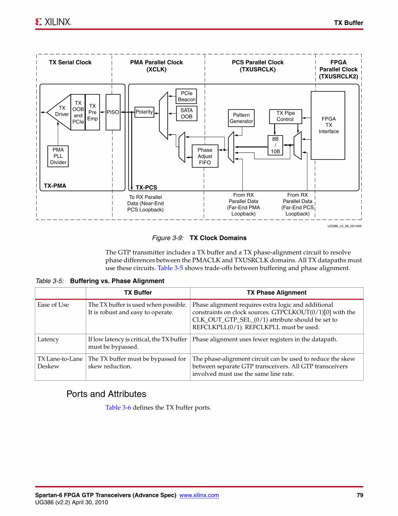
Spartan-6 FPGA GTP Transceivers (Advance Spec) www.xilinx.com 79UG386 (v2.2) April 30, 2010
TX Buffer
The GTP transmitter includes a TX buffer and a TX phase-alignment circuit to resolve phase differences between the PMACLK and TXUSRCLK domains. All TX datapaths must use these circuits. Table 3-5 shows trade-offs between buffering and phase alignment.
Ports and AttributesTable 3-6 defines the TX buffer ports.
X-Ref Target - Figure 3-9
Figure 3-9: TX Clock Domains
TX Serial Clock
TX-PMA TX-PCS
TXDriver
PMAPLL
Divider
TXOOBandPCIe
PISO Polarity
PhaseAdjustFIFO
PatternGenerator
8B/
10B
TX PipeControl FPGA
TXInterface
PMA Parallel Clock(XCLK)
PCS Parallel Clock(TXUSRCLK)
FPGAParallel Clock(TXUSRCLK2)
UG386_c3_06_051409
SATAOOB
TXPreEmp
PCIeBeacon
From RXParallel Data(Far-End PCS
Loopback)
From RXParallel Data
(Far-End PMALoopback)
To RX ParallelData (Near-EndPCS Loopback)
Table 3-5: Buffering vs. Phase Alignment
TX Buffer TX Phase Alignment
Ease of Use The TX buffer is used when possible. It is robust and easy to operate.
Phase alignment requires extra logic and additional constraints on clock sources. GTPCLKOUT(0/1)[0] with the CLK_OUT_GTP_SEL_(0/1) attribute should be set to REFCLKPLL(0/1). REFCLKPLL must be used.
Latency If low latency is critical, the TX buffer must be bypassed.
Phase alignment uses fewer registers in the datapath.
TX Lane-to-Lane Deskew
The TX buffer must be bypassed for skew reduction.
The phase-alignment circuit can be used to reduce the skew between separate GTP transceivers. All GTP transceivers involved must use the same line rate.
80 www.xilinx.com Spartan-6 FPGA GTP Transceivers (Advance Spec)UG386 (v2.2) April 30, 2010
Chapter 3: Transmitter
Table 3-6 defines the TX buffer attributes.
Using the TX BufferTo use the TX buffer to resolve phase differences between the domains, TX_BUFFER_USE must be set to TRUE. The buffer should be reset whenever TXBUFSTATUS indicates an overflow or an underflow. The buffer can be reset using GTPRESET or TXRESET. Assertion of GTPRESET triggers a sequence that resets the entire TX of the GTP transceiver.
Table 3-6: TX Buffer Ports
Port Dir Clock Domain Description
TXOUTCLK0
TXOUTCLK1
Out N/A This port provides a parallel clock generated by the GTP transceiver. This clock can be used to drive TXUSRCLK for one or more GTP transceivers. The clock rate depends on INTDATAWIDTH:
• INTDATAWIDTH is Low: FTXOUTCLK = Line Rate/8• INTDATAWIDTH is High: FTXOUTCLK = Line Rate/10
Note: When INTDATAWIDTH is High, the duty cycle is 60/40 instead of 50/50. TXOUTCLK cannot drive TXUSRCLK when the TX phase-alignment circuit is used.
TXRESET0
TXRESET1
In Asynchronous PCS TX system reset. Resets receiver TX FIFO, 8B/10B encoder and other transmitter registers. This reset is a subset of GTPRESET.
TXBUFSTATUS0[1:0]
TXBUFSTATUS1[1:0]
Out TXUSRCLK2 TX buffer status.
TXBUFSTATUS[1]: TX buffer overflow or underflow
1: FIFO has overflowed or underflowed
0: No overflow/underflow error
TXBUFSTATUS[0]: TX buffer fullness
1: FIFO is at least half full
0: FIFO is less than half full
If TXBUFSTATUS[1] goes High, it remains High until TXRESET is asserted.
Table 3-7: TX Buffer Attributes
Attribute Type Description
TX_BUFFER_USE_0
TX_BUFFER_USE_1
Boolean Determines whether the TX buffer is used or bypassed.
TRUE: Use the TX buffer (normal mode).
FALSE: Bypass the TX buffer (advance feature).
TX_XCLK_SEL_0
TX_XCLK_SEL_1
String Selects the clock used to drive the TX PMA parallel clock domain (XCLK) following the TX buffer. When using the TX buffer, this attribute is set to TXOUT.
The attribute must be set as follows:
TXOUT: Use when TX_BUFFER_USE = TRUE
TXUSR: Use when TX_BUFFER_USE = FALSE
TXRX_INVERT_0
TXRX_INVERT_1
3-bit Binary
Determines if fast capture latches are used or bypassed between the PMA and the PCS. The default value is 3'b111.
Spartan-6 FPGA GTP Transceivers (Advance Spec) www.xilinx.com 81UG386 (v2.2) April 30, 2010
TX Buffer Bypass
TX Buffer Bypass
Functional DescriptionAn advanced feature of the Spartan-6 FPGA GTP transceiver is bypassing the TX buffer. This is not recommended for normal operation. When the TX buffer is bypassed, a process called TX phase alignment must be performed to match or adjust the phase difference between the PMA parallel clock domain (XCLK) and the PCS parallel clock domain (TXUSRCLK). In addition to the TX phase alignment process, utilizing the GTPCLKFBWEST and GTPCLKFBEAST dedicated feedback paths from the GTP transceiver to a DCM or PLL adjusts TXUSRCLK to compensate for temperature and voltage variations. Figure 3-9, page 79 shows the XCLK and TXUSRCLK domains. Table 3-5, page 79 shows the trade-offs between the buffer and the buffer bypass modes.
Ports and AttributesTable 3-8 defines the TX buffer bypass ports.
Table 3-8: TX Buffer Bypass Ports
Port Dir Clock Domain Description
GTPCLKFBEAST[1:0] Out N/A Dedicated feedback clocks for PLL or DCM to adjust USRCLK for voltage and temperature variations in TX buffer bypass mode. This feedback path is independently selectable from TXUSRCLK(0/1) and RXUSRCLK(0/1).
GTPCLKFBSEL0EAST[1:0]
GTPCLKFBSEL1EAST[1:0]
In Async GTPCLKFBSEL0EAST is the dedicated feedback clock selectors for GTPCLKFBEAST[0]. GTPCLKFBSEL1EAST is the dedicated feedback clock selectors for GTPCLKFBEAST[1].
00: TXUSRCLK0
01: RXUSRCLK0
10: TXUSRCLK1
11: RXUSRCLK1
GTPCLKFBSEL0WEST[1:0]
GTPCLKFBSEL1WEST[1:0]
In Async GTPCLKFBSEL0WEST is the dedicated feedback clock selector for GTPCLKFBWEST[0]. GTPCLKFBSEL1WEST is the dedicated feedback clock selector for GTPCLKFBWEST[1].
00: TXUSRCLK0
01: RXUSRCLK0
10: TXUSRCLK1
11: RXUSRCLK1
GTPCLKFBWEST[1:0] Out N/A Dedicated feedback clocks for PLL or DCM to adjust USRCLK for voltage and temperature variations in TX buffer bypass mode. This feedback path is independently selectable from TXUSRCLK(0/1) and RXUSRCLK(0/1).
82 www.xilinx.com Spartan-6 FPGA GTP Transceivers (Advance Spec)UG386 (v2.2) April 30, 2010
Chapter 3: Transmitter
Table 3-9 defines the TX buffer bypass attributes.
GTPCLKOUT0[1:0]
GTPCLKOUT1[1:0]
Out N/A GTPCLKOUT is the recommended signal port to bring clocks inside the GTPA1_DUAL tile to the FPGA logic. GTPCLKOUT[0] must be used in TX Buffer Bypass mode.
GTPCLKOUT[0]: Outputs either TXOUTCLK or REFCLKPLL depending on CLK_OUT_GTP_SEL.
GTPCLKOUT[1]: Outputs RXRECCLK.
PLLLKDETEN0
PLLLKDETEN1
In Async Enables the PLL lock detector when High.
TXENPMAPHASEALIGN0
TXENPMAPHASEALIGN1
In Async When asserted High, the TX phase-alignment circuit is enabled, allowing XCLK to align with TXUSRCLK when TXPMASETPHASE is asserted. This also allows the XCLKs in multiple GTP transceivers to be synchronized to reduce TX lane-to-lane skew.
TXOUTCLK0
TXOUTCLK1
Out N/A These ports clock the TX logic between the PMA and the TX buffer. They are reserved for fabric output.
TXPMASETPHASE0
TXPMASETPHASE1
In Async When asserted High, the GTP transceiver aligns XCLK with TXUSRCLK, allowing the TX buffer to be bypassed.
TXUSRCLK0
TXUSRCLK1
In N/A Use this port to provide a clock for the internal TX PCS parallel datapath. This clock must always be provided.
Table 3-8: TX Buffer Bypass Ports (Cont’d)
Port Dir Clock Domain Description
Table 3-9: TX Buffer Bypass Attributes
Attribute Type Description
CLK_OUT_GTP_SEL_0
CLK_OUT_GTP_SEL_1
String Selects either TXOUTCLK or REFCLKPLL to be driven on GTPCLKOUT[0]. In TX Buffer Bypass mode, the source of TXUSRCLK and TXUSRCLK2 must come from REFCLKPLL.
Valid settings for CLK_OUT_GTP_SEL_0 are:
“TXOUTCLK0”
“REFCLKPLL0” (Required for TX Buffer Bypass)
Valid settings for CLK_OUT_GTP_SEL_1 are:
“TXOUTCLK1”
“REFCLKPLL1” (Required for TX Buffer Bypass)
PMA_TX_CFG0
PMA_TX_CFG1
20-bit Hex
TX channel specific settings. The default value is 20'h80082.
TX_BUFFER_USE_0
TX_BUFFER_USE_1
Boolean Determines whether the TX buffer is used or bypassed.
TRUE: Use the TX buffer (normal mode).
FALSE: Bypass the TX buffer (advance mode).
Spartan-6 FPGA GTP Transceivers (Advance Spec) www.xilinx.com 83UG386 (v2.2) April 30, 2010
TX Buffer Bypass
Using the TX Phase-Alignment Circuit to Bypass the TX BufferIf TX_BUFFER_USE is set to FALSE, the TX phase-alignment circuit must be used. The following procedure is recommended to use the TX phase-alignment circuit to force the PMA parallel clock (XCLK) phase to match the PCS parallel clock (TXUSRCLK) phase:
1. Set CLK_OUT_GTP_SEL to REFCLKPLL.
2. Set TX_XCLK_SEL to TXUSR.
3. Set TXRX_INVERT to 111 and set PMA_TX_CFG to 80082 hex.
4. Wait for all clock and lock signals to stabilize before asserting TXENPMAPHASEALIGN High.
5. Wait until TXENPMAPHASEALIGN is asserted for 512 TXUSRCLK2 clock cycles before asserting TXPMASETPHASE High.
6. Wait the number of required TXUSERCLK2 clock cycles as specified in Table 3-10 before deasserting TXPMASETPHASE.
7. Keep TXENPMAPHASEALIGN asserted unless the TX phase-alignment procedure must be repeated. Deasserting TXENPMAPHASEALIGN causes TX phase alignment to be lost.
8. After completing the TX phase-alignment procedure, the phase of the PMA parallel clock (XCLK) is aligned with the PCS parallel clock (TXUSRCLK).
The TX phase-alignment procedure must be repeated if any of the following conditions occur:
• GTPRESET0 or GTPRESET1 is asserted
• PLLPOWERDOWN is deasserted
• The clocking source is changed
• The line rate of the GTP transceiver is changed
Figure 3-10 shows the TX phase-alignment procedure after a GTPRESET. After GTPRESET completes, wait until RESETDONE and PLLLKDET go High, and all clocks stabilize before
TXRX_INVERT_0
TXRX_INVERT_1
3-bit Binary
Determines if fast capture latches are used or bypassed between the PMA and the PCS. The default value is 3'b111.
TX_XCLK_SEL_0
TX_XCLK_SEL_1
String Selects the clock used to drive the TX PMA parallel clock domain (XCLK) following the TX buffer. In TX Buffer Bypass mode, this attribute must be set to TXUSR.
TXOUT: Use when TX_BUFFER_USE = TRUE
TXUSR: Use when TX_BUFFER_USE = FALSE
Table 3-9: TX Buffer Bypass Attributes (Cont’d)
Attribute Type Description
Table 3-10: Required TXUSERCLK2 Wait Cycles for TXPMASETPHASE
PLL_TXDIVSEL_OUT TXUSRCLK2 Wait Cycles for TXPMASETPHASE
1 4,096
2 8,192
4 16,384
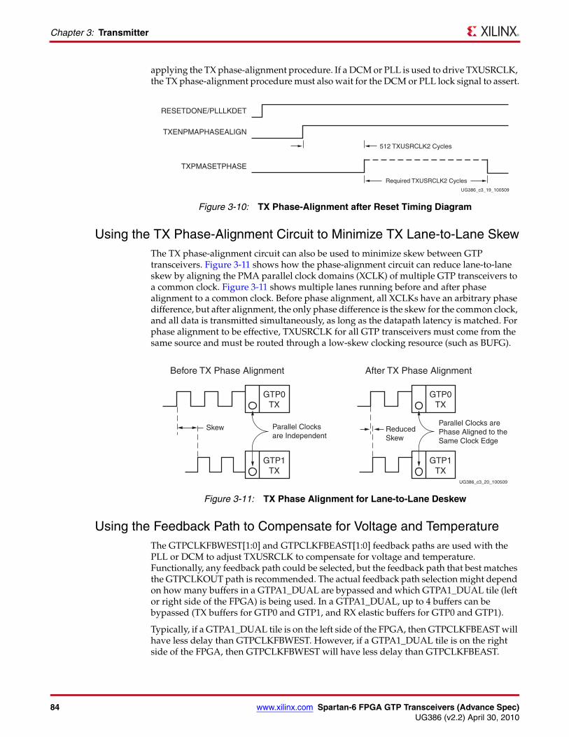
84 www.xilinx.com Spartan-6 FPGA GTP Transceivers (Advance Spec)UG386 (v2.2) April 30, 2010
Chapter 3: Transmitter
applying the TX phase-alignment procedure. If a DCM or PLL is used to drive TXUSRCLK, the TX phase-alignment procedure must also wait for the DCM or PLL lock signal to assert.
Using the TX Phase-Alignment Circuit to Minimize TX Lane-to-Lane SkewThe TX phase-alignment circuit can also be used to minimize skew between GTP transceivers. Figure 3-11 shows how the phase-alignment circuit can reduce lane-to-lane skew by aligning the PMA parallel clock domains (XCLK) of multiple GTP transceivers to a common clock. Figure 3-11 shows multiple lanes running before and after phase alignment to a common clock. Before phase alignment, all XCLKs have an arbitrary phase difference, but after alignment, the only phase difference is the skew for the common clock, and all data is transmitted simultaneously, as long as the datapath latency is matched. For phase alignment to be effective, TXUSRCLK for all GTP transceivers must come from the same source and must be routed through a low-skew clocking resource (such as BUFG).
Using the Feedback Path to Compensate for Voltage and TemperatureThe GTPCLKFBWEST[1:0] and GTPCLKFBEAST[1:0] feedback paths are used with the PLL or DCM to adjust TXUSRCLK to compensate for voltage and temperature. Functionally, any feedback path could be selected, but the feedback path that best matches the GTPCLKOUT path is recommended. The actual feedback path selection might depend on how many buffers in a GTPA1_DUAL are bypassed and which GTPA1_DUAL tile (left or right side of the FPGA) is being used. In a GTPA1_DUAL, up to 4 buffers can be bypassed (TX buffers for GTP0 and GTP1, and RX elastic buffers for GTP0 and GTP1).
Typically, if a GTPA1_DUAL tile is on the left side of the FPGA, then GTPCLKFBEAST will have less delay than GTPCLKFBWEST. However, if a GTPA1_DUAL tile is on the right side of the FPGA, then GTPCLKFBWEST will have less delay than GTPCLKFBEAST.
X-Ref Target - Figure 3-10
Figure 3-10: TX Phase-Alignment after Reset Timing Diagram
UG386_c3_19_100509
RESETDONE/PLLLKDET
TXENPMAPHASEALIGN
TXPMASETPHASE
512 TXUSRCLK2 Cycles
Required TXUSRCLK2 Cycles
X-Ref Target - Figure 3-11
Figure 3-11: TX Phase Alignment for Lane-to-Lane Deskew
UG386_c3_20_100509
Before TX Phase Alignment
Skew Parallel Clocksare Independent
GTP0TX
GTP1TX
After TX Phase Alignment
ReducedSkew
Parallel Clocks arePhase Aligned to theSame Clock Edge
GTP0TX
GTP1TX
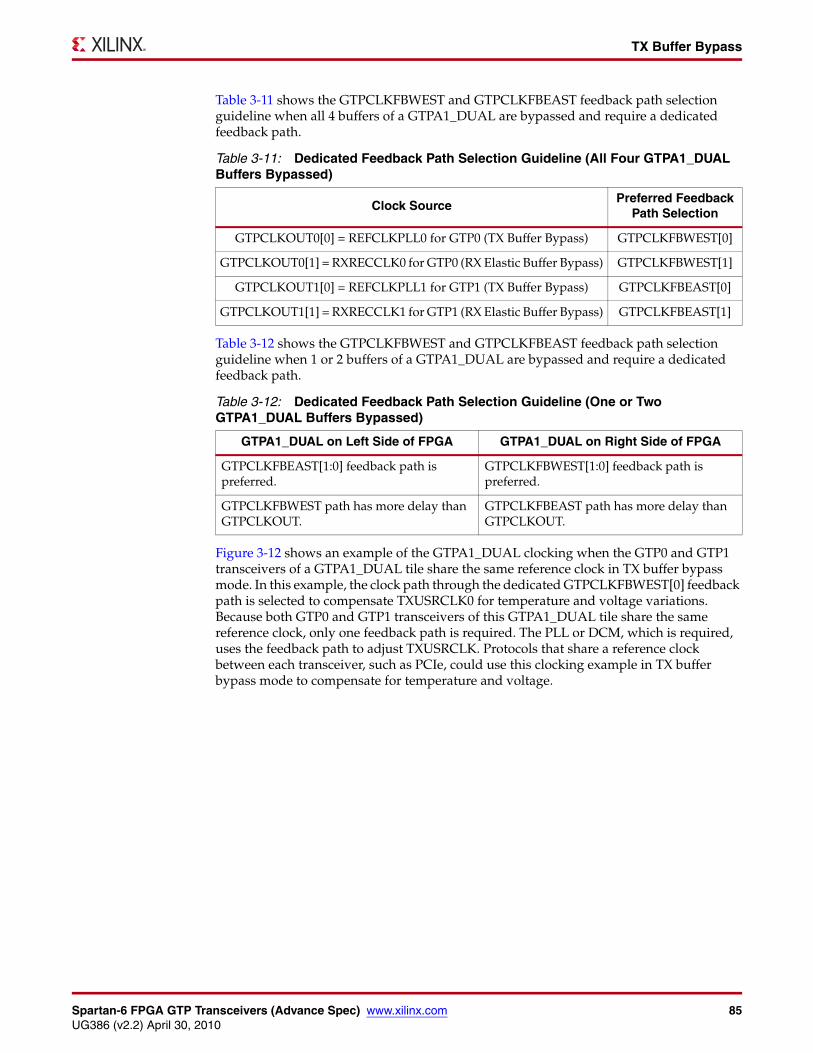
Spartan-6 FPGA GTP Transceivers (Advance Spec) www.xilinx.com 85UG386 (v2.2) April 30, 2010
TX Buffer Bypass
Table 3-11 shows the GTPCLKFBWEST and GTPCLKFBEAST feedback path selection guideline when all 4 buffers of a GTPA1_DUAL are bypassed and require a dedicated feedback path.
Table 3-12 shows the GTPCLKFBWEST and GTPCLKFBEAST feedback path selection guideline when 1 or 2 buffers of a GTPA1_DUAL are bypassed and require a dedicated feedback path.
Figure 3-12 shows an example of the GTPA1_DUAL clocking when the GTP0 and GTP1 transceivers of a GTPA1_DUAL tile share the same reference clock in TX buffer bypass mode. In this example, the clock path through the dedicated GTPCLKFBWEST[0] feedback path is selected to compensate TXUSRCLK0 for temperature and voltage variations. Because both GTP0 and GTP1 transceivers of this GTPA1_DUAL tile share the same reference clock, only one feedback path is required. The PLL or DCM, which is required, uses the feedback path to adjust TXUSRCLK. Protocols that share a reference clock between each transceiver, such as PCIe, could use this clocking example in TX buffer bypass mode to compensate for temperature and voltage.
Table 3-11: Dedicated Feedback Path Selection Guideline (All Four GTPA1_DUAL Buffers Bypassed)
Clock SourcePreferred Feedback
Path Selection
GTPCLKOUT0[0] = REFCLKPLL0 for GTP0 (TX Buffer Bypass) GTPCLKFBWEST[0]
GTPCLKOUT0[1] = RXRECCLK0 for GTP0 (RX Elastic Buffer Bypass) GTPCLKFBWEST[1]
GTPCLKOUT1[0] = REFCLKPLL1 for GTP1 (TX Buffer Bypass) GTPCLKFBEAST[0]
GTPCLKOUT1[1] = RXRECCLK1 for GTP1 (RX Elastic Buffer Bypass) GTPCLKFBEAST[1]
Table 3-12: Dedicated Feedback Path Selection Guideline (One or Two GTPA1_DUAL Buffers Bypassed)
GTPA1_DUAL on Left Side of FPGA GTPA1_DUAL on Right Side of FPGA
GTPCLKFBEAST[1:0] feedback path is preferred.
GTPCLKFBWEST[1:0] feedback path is preferred.
GTPCLKFBWEST path has more delay than GTPCLKOUT.
GTPCLKFBEAST path has more delay than GTPCLKOUT.
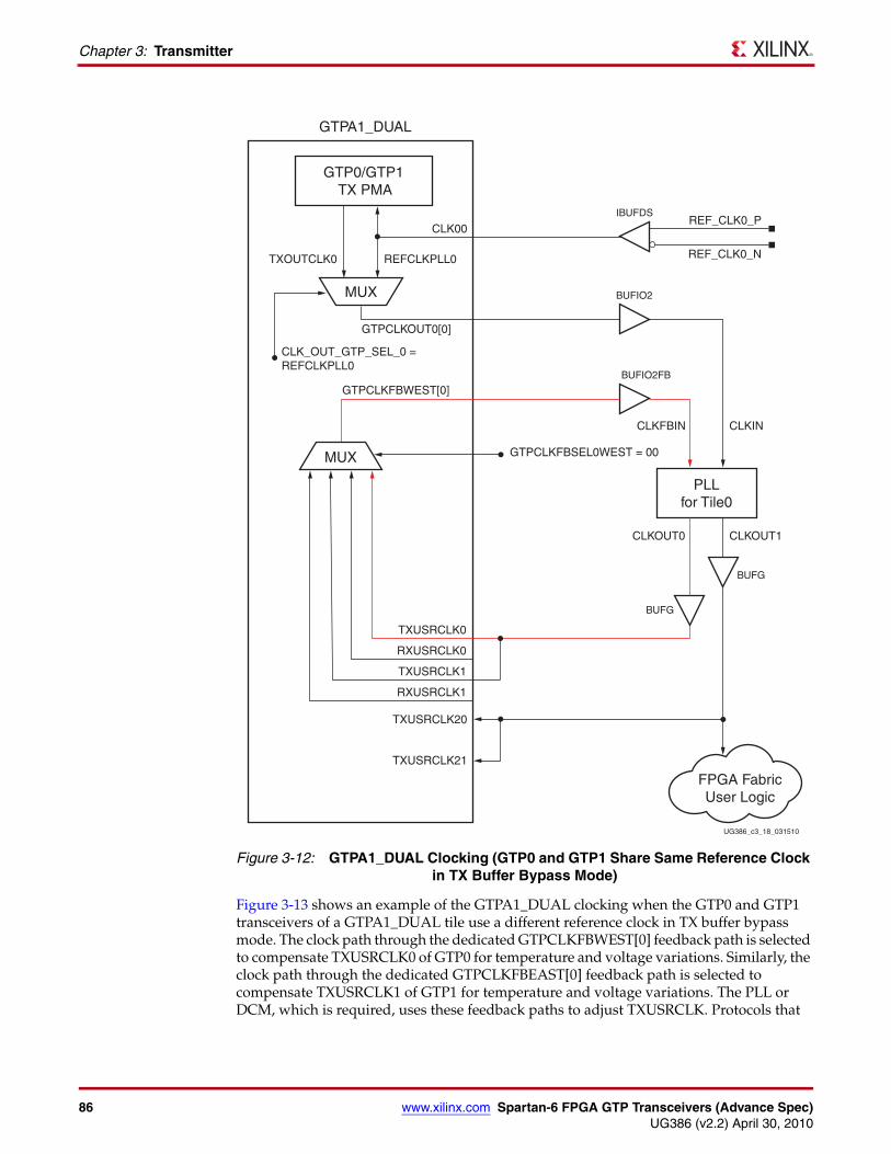
86 www.xilinx.com Spartan-6 FPGA GTP Transceivers (Advance Spec)UG386 (v2.2) April 30, 2010
Chapter 3: Transmitter
Figure 3-13 shows an example of the GTPA1_DUAL clocking when the GTP0 and GTP1 transceivers of a GTPA1_DUAL tile use a different reference clock in TX buffer bypass mode. The clock path through the dedicated GTPCLKFBWEST[0] feedback path is selected to compensate TXUSRCLK0 of GTP0 for temperature and voltage variations. Similarly, the clock path through the dedicated GTPCLKFBEAST[0] feedback path is selected to compensate TXUSRCLK1 of GTP1 for temperature and voltage variations. The PLL or DCM, which is required, uses these feedback paths to adjust TXUSRCLK. Protocols that
X-Ref Target - Figure 3-12
Figure 3-12: GTPA1_DUAL Clocking (GTP0 and GTP1 Share Same Reference Clock in TX Buffer Bypass Mode)
UG386_c3_18_031510
IBUFDSREF_CLK0_P
REF_CLK0_N
CLKIN
CLKOUT1
CLK00
GTPCLKOUT0[0]
TXOUTCLK0 REFCLKPLL0
GTPCLKFBWEST[0]
TXUSRCLK1
RXUSRCLK1
TXUSRCLK0
RXUSRCLK0
TXUSRCLK20
TXUSRCLK21
GTPCLKFBSEL0WEST = 00
CLK_OUT_GTP_SEL_0 = REFCLKPLL0
CLKFBIN
PLLfor Tile0
GTP0/GTP1 TX PMA
GTPA1_DUAL
MUX BUFIO2
BUFG
BUFIO2FB
CLKOUT0
BUFG
MUX
FPGA FabricUser Logic
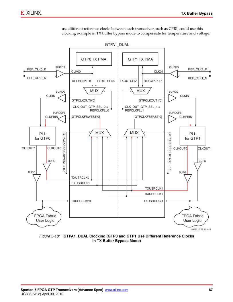
Spartan-6 FPGA GTP Transceivers (Advance Spec) www.xilinx.com 87UG386 (v2.2) April 30, 2010
TX Buffer Bypass
use different reference clocks between each transceiver, such as CPRI, could use this clocking example in TX buffer bypass mode to compensate for temperature and voltage.
X-Ref Target - Figure 3-13
Figure 3-13: GTPA1_DUAL Clocking (GTP0 and GTP1 Use Different Reference Clocks in TX Buffer Bypass Mode)
UG386_c3_20_031610
IBUFDSREF_CLK1_P
REF_CLK1_N
CLKIN
CLK01CLK00
GTPCLKOUT1[0]
TXOUTCLK1 REFCLKPLL1
GTPCLKFBEAST[0]
TXUSRCLK1
RXUSRCLK1
TXUSRCLK21
GT
PC
LKF
BS
EL0E
AS
T =
10
CLK_OUT_GTP_SEL_1 = REFCLKPLL1
CLKFBIN
PLLfor GTP1
GTP1 TX PMA
MUX BUFIO2
BUFG
BUFIO2FB
BUFG
MUX
IBUFDSREF_CLK0_P
REF_CLK0_N
CLKIN
CLKOUT1
GTPCLKOUT0[0]
TXOUTCLK0REFCLKPLL0
GTPCLKFBWEST[0]
TXUSRCLK0
RXUSRCLK0
TXUSRCLK20
GT
PC
LKF
BS
EL0W
ES
T =
00
CLK_OUT_GTP_SEL_0 = REFCLKPLL0
CLKFBIN
PLLfor GTP0
GTP0 TX PMA
GTPA1_DUAL
MUXBUFIO2
BUFG
BUFIO2FB
CLKOUT0
BUFG
MUX
FPGA FabricUser Logic
FPGA FabricUser Logic
CLKOUT1CLKOUT0
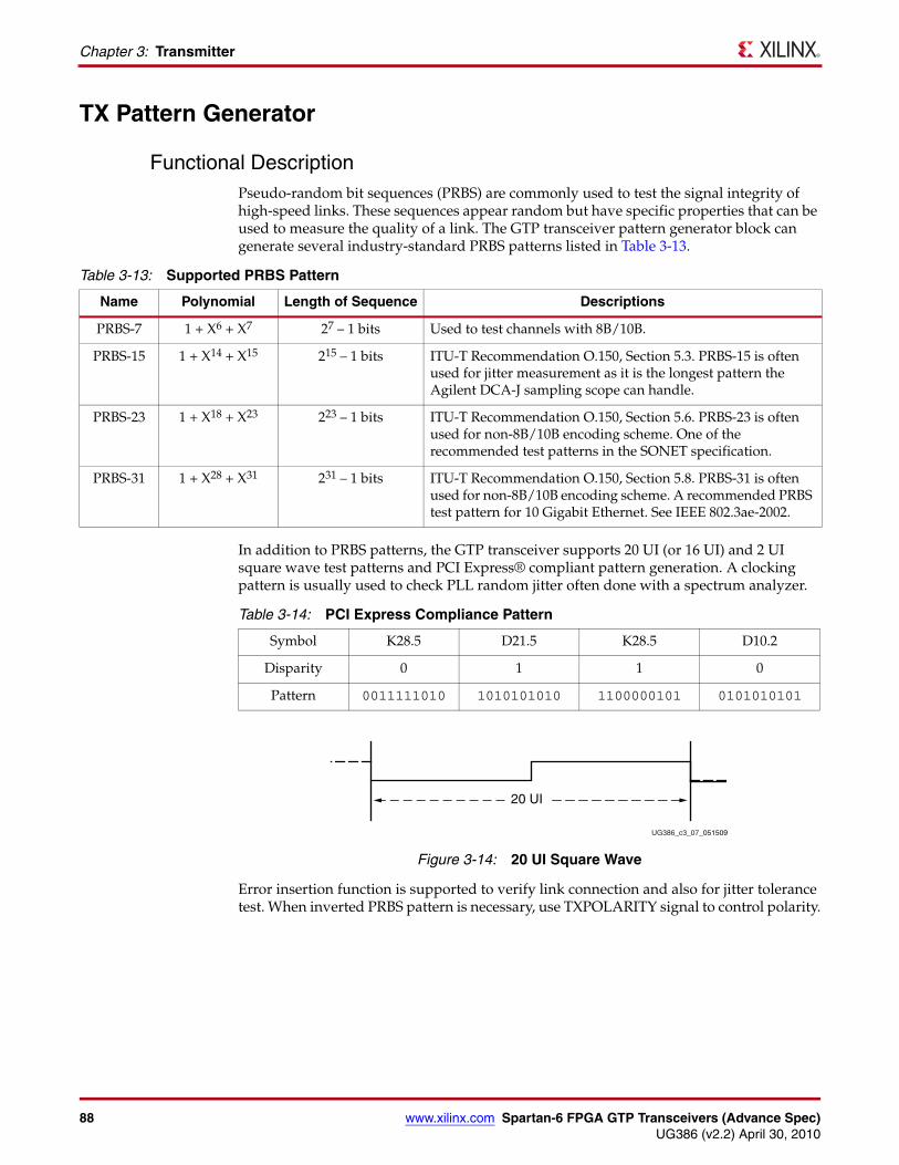
88 www.xilinx.com Spartan-6 FPGA GTP Transceivers (Advance Spec)UG386 (v2.2) April 30, 2010
Chapter 3: Transmitter
TX Pattern Generator
Functional DescriptionPseudo-random bit sequences (PRBS) are commonly used to test the signal integrity of high-speed links. These sequences appear random but have specific properties that can be used to measure the quality of a link. The GTP transceiver pattern generator block can generate several industry-standard PRBS patterns listed in Table 3-13.
In addition to PRBS patterns, the GTP transceiver supports 20 UI (or 16 UI) and 2 UI square wave test patterns and PCI Express® compliant pattern generation. A clocking pattern is usually used to check PLL random jitter often done with a spectrum analyzer.
Error insertion function is supported to verify link connection and also for jitter tolerance test. When inverted PRBS pattern is necessary, use TXPOLARITY signal to control polarity.
Table 3-13: Supported PRBS Pattern
Name Polynomial Length of Sequence Descriptions
PRBS-7 1 + X6 + X7 27 – 1 bits Used to test channels with 8B/10B.
PRBS-15 1 + X14 + X15 215 – 1 bits ITU-T Recommendation O.150, Section 5.3. PRBS-15 is often used for jitter measurement as it is the longest pattern the Agilent DCA-J sampling scope can handle.
PRBS-23 1 + X18 + X23 223 – 1 bits ITU-T Recommendation O.150, Section 5.6. PRBS-23 is often used for non-8B/10B encoding scheme. One of the recommended test patterns in the SONET specification.
PRBS-31 1 + X28 + X31 231 – 1 bits ITU-T Recommendation O.150, Section 5.8. PRBS-31 is often used for non-8B/10B encoding scheme. A recommended PRBS test pattern for 10 Gigabit Ethernet. See IEEE 802.3ae-2002.
Table 3-14: PCI Express Compliance Pattern
Symbol K28.5 D21.5 K28.5 D10.2
Disparity 0 1 1 0
Pattern 0011111010 1010101010 1100000101 0101010101
X-Ref Target - Figure 3-14
Figure 3-14: 20 UI Square Wave
UG386_c3_07_051509
20 UI
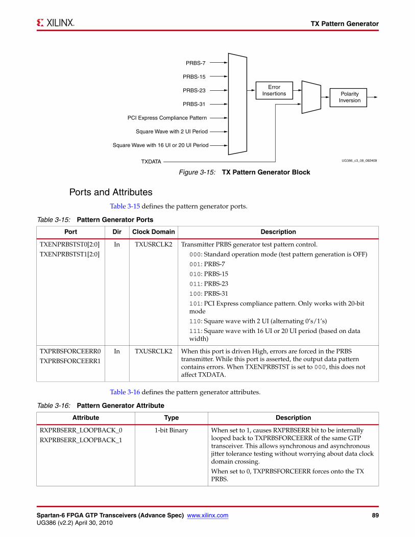
Spartan-6 FPGA GTP Transceivers (Advance Spec) www.xilinx.com 89UG386 (v2.2) April 30, 2010
TX Pattern Generator
Ports and AttributesTable 3-15 defines the pattern generator ports.
Table 3-16 defines the pattern generator attributes.
X-Ref Target - Figure 3-15
Figure 3-15: TX Pattern Generator Block
UG386_c3_08_092409TXDATA
ErrorInsertions Polarity
Inversion
PRBS-7
PRBS-15
PRBS-23
PRBS-31
PCI Express Compliance Pattern
Square Wave with 2 UI Period
Square Wave with 16 UI or 20 UI Period
Table 3-15: Pattern Generator Ports
Port Dir Clock Domain Description
TXENPRBSTST0[2:0]
TXENPRBSTST1[2:0]
In TXUSRCLK2 Transmitter PRBS generator test pattern control.
000: Standard operation mode (test pattern generation is OFF)
001: PRBS-7
010: PRBS-15
011: PRBS-23
100: PRBS-31
101: PCI Express compliance pattern. Only works with 20-bit mode
110: Square wave with 2 UI (alternating 0’s/1’s)
111: Square wave with 16 UI or 20 UI period (based on data width)
TXPRBSFORCEERR0
TXPRBSFORCEERR1
In TXUSRCLK2 When this port is driven High, errors are forced in the PRBS transmitter. While this port is asserted, the output data pattern contains errors. When TXENPRBSTST is set to 000, this does not affect TXDATA.
Table 3-16: Pattern Generator Attribute
Attribute Type Description
RXPRBSERR_LOOPBACK_0
RXPRBSERR_LOOPBACK_1
1-bit Binary When set to 1, causes RXPRBSERR bit to be internally looped back to TXPRBSFORCEERR of the same GTP transceiver. This allows synchronous and asynchronous jitter tolerance testing without worrying about data clock domain crossing.
When set to 0, TXPRBSFORCEERR forces onto the TX PRBS.
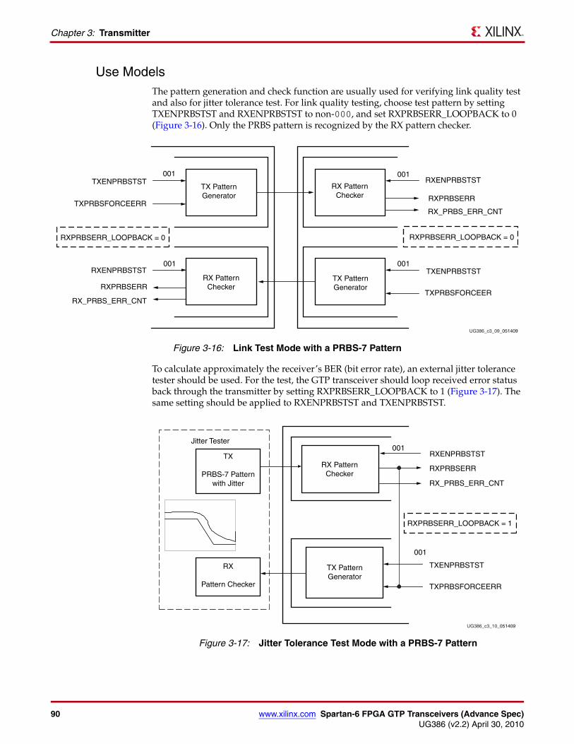
90 www.xilinx.com Spartan-6 FPGA GTP Transceivers (Advance Spec)UG386 (v2.2) April 30, 2010
Chapter 3: Transmitter
Use ModelsThe pattern generation and check function are usually used for verifying link quality test and also for jitter tolerance test. For link quality testing, choose test pattern by setting TXENPRBSTST and RXENPRBSTST to non-000, and set RXPRBSERR_LOOPBACK to 0 (Figure 3-16). Only the PRBS pattern is recognized by the RX pattern checker.
To calculate approximately the receiver’s BER (bit error rate), an external jitter tolerance tester should be used. For the test, the GTP transceiver should loop received error status back through the transmitter by setting RXPRBSERR_LOOPBACK to 1 (Figure 3-17). The same setting should be applied to RXENPRBSTST and TXENPRBSTST.
X-Ref Target - Figure 3-16
Figure 3-16: Link Test Mode with a PRBS-7 Pattern
UG386_c3_09_051409
TX PatternGenerator
RX PatternChecker
001
001
RX PatternChecker
TX PatternGenerator
001
001
RXPRBSERR_LOOPBACK = 0
TXENPRBSTST
TXPRBSFORCEERR
RXENPRBSTST
RXPRBSERR
RX_PRBS_ERR_CNT
RXENPRBSTST
RXPRBSERR
RX_PRBS_ERR_CNT
RXPRBSERR_LOOPBACK = 0
TXENPRBSTST
TXPRBSFORCEER
X-Ref Target - Figure 3-17
Figure 3-17: Jitter Tolerance Test Mode with a PRBS-7 Pattern
UG386_c3_10_051409
RX PatternChecker
TX PatternGenerator
RXENPRBSTST001
RXPRBSERR
TXENPRBSTST
TXPRBSFORCEERR
001
Jitter Tester
TX
PRBS-7 Patternwith Jitter
RX
Pattern Checker
RXPRBSERR_LOOPBACK = 1
RX_PRBS_ERR_CNT
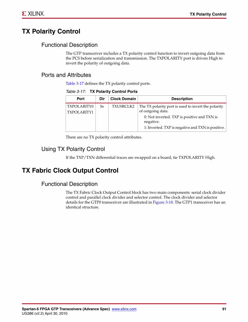
Spartan-6 FPGA GTP Transceivers (Advance Spec) www.xilinx.com 91UG386 (v2.2) April 30, 2010
TX Polarity Control
TX Polarity Control
Functional DescriptionThe GTP transceiver includes a TX polarity control function to invert outgoing data from the PCS before serialization and transmission. The TXPOLARITY port is driven High to invert the polarity of outgoing data.
Ports and AttributesTable 3-17 defines the TX polarity control ports.
There are no TX polarity control attributes.
Using TX Polarity ControlIf the TXP/TXN differential traces are swapped on a board, tie TXPOLARITY High.
TX Fabric Clock Output Control
Functional DescriptionThe TX Fabric Clock Output Control block has two main components: serial clock divider control and parallel clock divider and selector control. The clock divider and selector details for the GTP0 transceiver are illustrated in Figure 3-18. The GTP1 transceiver has an identical structure.
Table 3-17: TX Polarity Control Ports
Port Dir Clock Domain Description
TXPOLARITY0
TXPOLARITY1
In TXUSRCLK2 The TX polarity port is used to invert the polarity of outgoing data.
0: Not inverted. TXP is positive and TXN is negative.
1: Inverted. TXP is negative and TXN is positive.
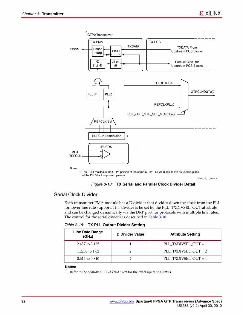
92 www.xilinx.com Spartan-6 FPGA GTP Transceivers (Advance Spec)UG386 (v2.2) April 30, 2010
Chapter 3: Transmitter
Serial Clock Divider
Each transmitter PMA module has a D divider that divides down the clock from the PLL for lower line rate support. This divider is be set by the PLL_TXDIVSEL_OUT attribute and can be changed dynamically via the DRP port for protocols with multiple line rates. The control for the serial divider is described in Table 3-18.
X-Ref Target - Figure 3-18
Figure 3-18: TX Serial and Parallel Clock Divider Detail
UG386_c3_11_051409
TX PMA TX PCS
GTPCLKOUT0[0]
TXDATA
PISO
REFCLK Distribution
O
REFCLK Sel
Notes: 1. The PLL1 resides in the GTP1 portion of the same GTPA1_DUAL block. It can be used in place of the PLL0 for low-power operation.
GTP0 Transceiver
TXP/N PhaseInterp
TXDATA FromUpstream PCS Blocks
Parallel Clock forUpstream PCS Blocks
/4 or/5
/D{1,2,4}
TXOUTCLK0
REFCLKPLL0
CLK_OUT_GTP_SEL_0 (Attribute)
PLL0PLL1(1)
IBUFDS
MGTREFCLK
Table 3-18: TX PLL Output Divider Setting
Line Rate Range(GHz)
D Divider Value Attribute Setting
2.457 to 3.125 1 PLL_TXDIVSEL_OUT = 1
1.2288 to 1.62 2 PLL_TXDIVSEL_OUT = 2
0.614 to 0.810 4 PLL_TXDIVSEL_OUT = 4
Notes: 1. Refer to the Spartan-6 FPGA Data Sheet for the exact operating limits.
Spartan-6 FPGA GTP Transceivers (Advance Spec) www.xilinx.com 93UG386 (v2.2) April 30, 2010
TX Fabric Clock Output Control
Parallel Clock Divider and Selector
The parallel clock output, TXOUTCLK, from the TX Fabric Clock Output Control block can be used as a fabric logic clock. TXOUTCLK is a 1-byte data width clock. Its frequency is line rate divided by 8 or 10 depending on the value of INTDATAWIDTH.
The CLK_OUT_GTP_SEL attribute controls the input selector and allows the following clocks to be output via GTPCLKOUT[0] port:
• TXOUTCLK: This clock, which is the divided-down PLL clock after the TX phase interpolator, is used by the TX PCS block. The TX phase interpolator is used to match the phase of the internal clock to the FPGA logic clock in TX buffer bypass mode.
• REFCLKPLL: This clock is the input reference clock to the PLL. REFCLKPLL is the recommended clock for general usage and is required for TX buffer bypass mode.
The GTPA1_DUAL primitive contains additional clock output ports: REFCLKOUT, REFCLKPLL, TXOUTCLK, and RXRECCLK. These clock outputs are reserved and not recommended for use. GTPCLKOUT should be used instead.
Ports and AttributesTable 3-19 defines the TX Fabric Clock Output Control block ports.
Table 3-19: TX Fabric Clock Output Control Ports
Port Dir Clock Domain Description
GTPCLKOUT0[1:0]
GTPCLKOUT1[1:0]
Out N/A GTPCLKOUT(0/1) is the recommended signal port to bring clocks inside the GTPA1_DUAL tile to the FPGA logic.
Bit 0 of GTPCLKOUT(0/1) allows the user to output either TXOUTCLK(0/1) or REFCLKPLL(0/1). CLK_OUT_GTP_SEL_(0/1) selects the clock to be output.
Bit 1 of GTPCLKOUT(0/1) outputs RXRECCLK(0/1).
INTDATAWIDTH0
INTDATAWIDTH1
In Async This port specifies the width of the internal datapath and the value of the parallel clock divider for both the TX and the RX datapaths of the same GTP lane.
0: Internal datapath is 8 bits wide and the parallel clock divider is set to 4.
1: Internal datapath is 10 bits wide and the parallel clock divider is set to 5.
Because INTDATAWIDTH(0/1) also controls the PLL feedback divider N1, when a PLL is shared between the two lanes within the GTPA1_DUAL tile, the INTDATAWIDTH(0/1) ports in both lanes must be set to the same value.
REFCLKOUT0
REFCLKOUT1
Out N/A Reserved. GTPCLKOUT(0/1)[0] should be used instead.
94 www.xilinx.com Spartan-6 FPGA GTP Transceivers (Advance Spec)UG386 (v2.2) April 30, 2010
Chapter 3: Transmitter
Table 3-20 defines the TX Fabric Clock Output Control block attributes.
TX Configurable Driver
Functional DescriptionThe GTP TX driver is a high-speed current-mode differential output buffer. To maximize signal integrity, it includes these features:
• Differential voltage control
• Pre-cursor transmit pre-emphasis
• Configurable termination resistors
REFCLKPLL0
REFCLKPLL1
Out N/A If multiple reference clocks are used to a particular GTP transceiver, these ports must be used to manually connect the reference clock of one GTPA1_DUAL to the CLKINEAST/CLKINWEST of the other GTP transceiver. Thus the IBUFDS element is near one GTPA1_DUAL, which forwards its clock to the other GTPA1_DUAL, and the GTP transceivers share a reference clock.
If one reference clock is used, software uses this port to automatically cascade the reference clock between the GTPA1_DUAL tiles (if needed for the design as specified by LOC constraints or connections between IBUFDS and GTPA1_DUAL elements). Then this output can be left unconnected in the design.
TXOUTCLK0
TXOUTCLK1
Out N/A Reserved. GTPCLKOUT(0/1)[0] should be used instead.
Table 3-19: TX Fabric Clock Output Control Ports (Cont’d)
Port Dir Clock Domain Description
Table 3-20: TX Fabric Clock Output Control Attributes
Attribute Type Description
CLK_OUT_GTP_SEL_0
CLK_OUT_GTP_SEL_1
String This attribute is the multiplexer select signal in Figure 3-18, page 92. It determines which GTP transceiver (GTP0/GTP1) internal clock is output to the FPGA logic via the GTPCLKOUT(0/1) signal port.
Valid settings for CLK_OUT_GTP_SEL_0 are:
“TXOUTCLK0”
“REFCLKPLL0”
Valid settings for CLK_OUT_GTP_SEL_1 are:
“TXOUTCLK1”
“REFCLKPLL1”
PLL_TXDIVSEL_OUT Integer This attributes controls the setting for the TX serial clock divider for low line rate support (see Table 3-18, page 92). Valid settings are:
1: Set the D divider to 1
2: Set the D divider to 2
4: Set the D divider to 4
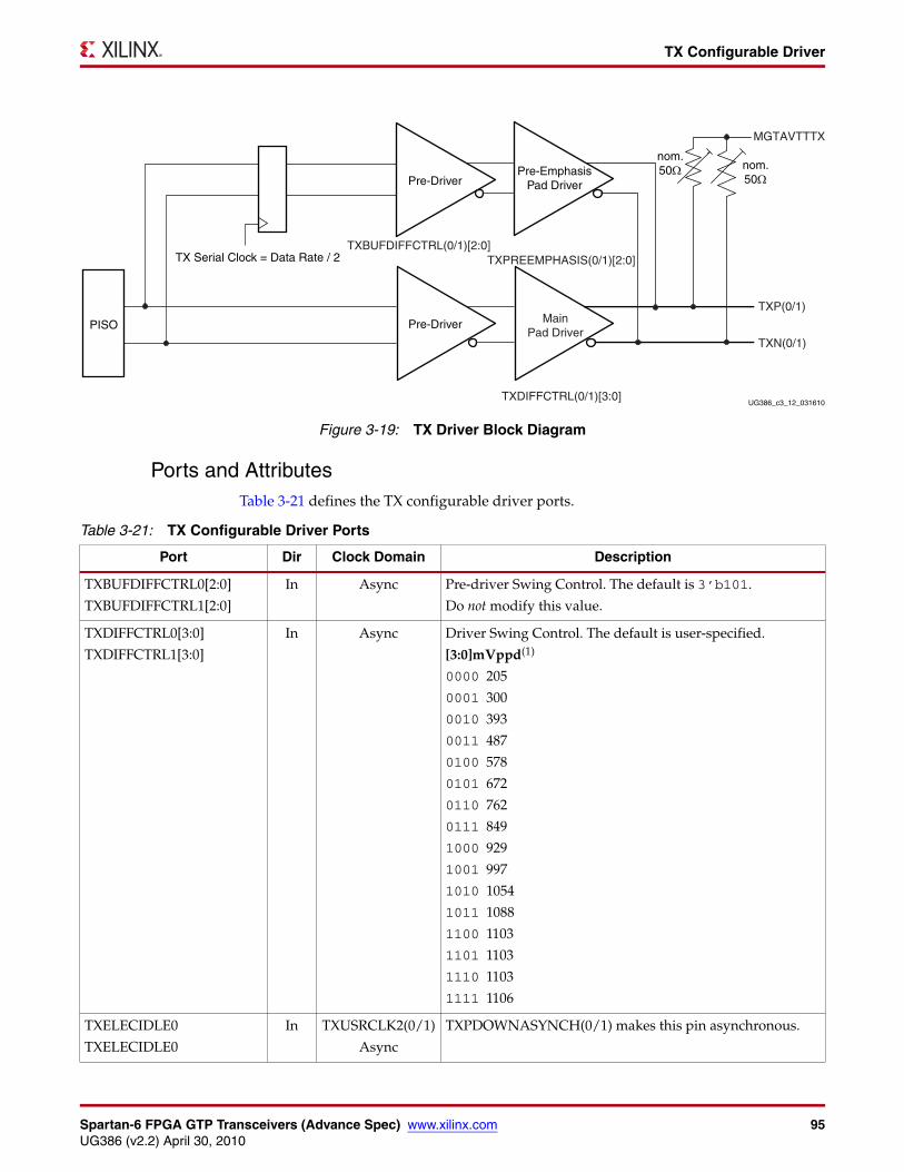
Spartan-6 FPGA GTP Transceivers (Advance Spec) www.xilinx.com 95UG386 (v2.2) April 30, 2010
TX Configurable Driver
Ports and AttributesTable 3-21 defines the TX configurable driver ports.
X-Ref Target - Figure 3-19
Figure 3-19: TX Driver Block Diagram
UG386_c3_12_031610
TXP(0/1)
TXN(0/1)
PISO
Pre-DriverPre-Emphasis
Pad Driver
Pre-Driver MainPad Driver
TXPREEMPHASIS(0/1)[2:0]TXBUFDIFFCTRL(0/1)[2:0]
TXDIFFCTRL(0/1)[3:0]
MGTAVTTTX
nom.50Ω
nom.50Ω
TX Serial Clock = Data Rate / 2
Table 3-21: TX Configurable Driver Ports
Port Dir Clock Domain Description
TXBUFDIFFCTRL0[2:0]
TXBUFDIFFCTRL1[2:0]
In Async Pre-driver Swing Control. The default is 3’b101.
Do not modify this value.
TXDIFFCTRL0[3:0]
TXDIFFCTRL1[3:0]
In Async Driver Swing Control. The default is user-specified.
[3:0]mVppd(1)
0000 205
0001 300
0010 393
0011 487
0100 578
0101 672
0110 762
0111 849
1000 929
1001 997
1010 1054
1011 1088
1100 1103
1101 1103
1110 1103
1111 1106
TXELECIDLE0
TXELECIDLE0
In TXUSRCLK2(0/1)
Async
TXPDOWNASYNCH(0/1) makes this pin asynchronous.
96 www.xilinx.com Spartan-6 FPGA GTP Transceivers (Advance Spec)UG386 (v2.2) April 30, 2010
Chapter 3: Transmitter
There are no TX configurable driver attributes.
Use Modes – TX Driver
General
Based on the application requirement, TXDIFFCTRL and TXPREEMPHASIS values are set to the appropriate values.
Use Mode – Resistor CalibrationFor more information on the on-chip resistor calibration, refer to Termination Resistor Calibration Circuit, page 164.
TXINHIBIT0
TXINHIBIT1
In TXUSRCLK2(0/1) When High, this signal blocks transmission of TXDATA(0/1) and forces TXP(0/1) to 0 and TXN(0/1) to 1.
TXP0
TXP1
TXN0
TXN1
Out (Pad)
TX Serial Clock TXP(0/1) and TXN(0/1) are differential complements of one another forming a differential transmit output pair. These ports represent the pads. The locations of these ports must be constrained (see Implementation, page 26) and brought to the top level of the design.
TXPDOWNASYNCH0
TXPDOWNASYNCH1
In Async Determines if TXELECIDLE(0/1) and TXPOWERDOWN(0/1) should be treated as synchronous or asynchronous signals. Enables compliance during cold and warm PCI Express resets.
TXPREEMPHASIS0[2:0]
TXPREEMPHASIS1[2:0]
In Async Transmitter Post-Cursor TX Pre-Emphasis Control. The default is user specified.
[2:0]Pre-Emphasis (dB)(1)
000 0
001 0.8
010 1.7
011 2.5
100 3.5
101 4.5
110 6.1
111 7.6
Notes: 1. Nominal values. Refer to the Spartan-6 FPGA Data Sheet for the exact values based on marginal conditions.
Table 3-21: TX Configurable Driver Ports (Cont’d)
Port Dir Clock Domain Description
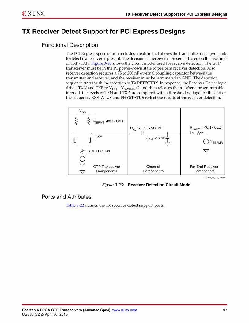
Spartan-6 FPGA GTP Transceivers (Advance Spec) www.xilinx.com 97UG386 (v2.2) April 30, 2010
TX Receiver Detect Support for PCI Express Designs
TX Receiver Detect Support for PCI Express Designs
Functional DescriptionThe PCI Express specification includes a feature that allows the transmitter on a given link to detect if a receiver is present. The decision if a receiver is present is based on the rise time of TXP/TXN. Figure 3-20 shows the circuit model used for receive detection. The GTP transceiver must be in the P1 power-down state to perform receiver detection. Also receiver detection requires a 75 to 200 nF external coupling capacitor between the transmitter and receiver, and the receiver must be terminated to GND. The detection sequence starts with the assertion of TXDETECTRX. In response, the Receiver Detect logic drives TXN and TXP to VDD – VSWING/2 and then releases them. After a programmable interval, the levels of TXN and TXP are compared with a threshold voltage. At the end of the sequence, RXSTATUS and PHYSTATUS reflect the results of the receiver detection.
Ports and AttributesTable 3-22 defines the TX receiver detect support ports.
X-Ref Target - Figure 3-20
Figure 3-20: Receiver Detection Circuit Model
CCH: < 3 nF
UG386_c3_13_051409
CAC: 75 nF - 200 nF RTERMR: 40Ω - 60Ω
VTERMR
RTERMT: 40Ω - 60Ω
VDD
TXDETECTRX
GTP TransceiverComponents
ChannelComponents
Far-End ReceiverComponents
TXP
98 www.xilinx.com Spartan-6 FPGA GTP Transceivers (Advance Spec)UG386 (v2.2) April 30, 2010
Chapter 3: Transmitter
There are no TX receiver detect support attributes.
Table 3-22: TX Receiver Detect Support Ports
Port Dir Clock Domain Description
PHYSTATUS0
PHYSTATUS1
Out Async This signal is asserted High to indicate completion of several PHY functions, including power management state transitions and receiver detection. When this signal transitions during entry and exit from P2 and RXUSRCLK2 is not running, the signaling is asynchronous.
RXSTATUS0[2:0]
RXSTATUS1[2:0]
Out RXUSRCLK2 PCIe usage only.
000: Receiver not present (when in receiver detection sequence)/Received data OK (during normal operation).
001: Reserved.
010: Reserved.
011: Receiver present (when in receiver detection sequence).
100: 8B/10B decode error.
101: Elastic buffer overflow. Different than defined in the PIPE specification.
110: Elastic buffer underflow. Different than defined in the PIPE specification.
111: Receive disparity error.
Refer to Table 3-23 for SATA usage of these bits.
TXDETECTRX0
TXDETECTRX1
In TXUSRCLK2 Activates the receive detection sequence. The sequence ends when PHYSTATUS is asserted to indicate that the results of the test are ready on RXSTATUS.
When RXSTATUS = 000, the receiver is not detected. When RXSTATUS = 011, the receiver is detected.
RXPOWERDOWN0[1:0]
RXPOWERDOWN1[1:0]
In Async Controls the power state of the TX and RX links. The encoding complies with the PCI Express specification encoding. TX and RX can be powered down separately. However, for PCI Express compliance, TXPOWERDOWN and RXPOWERDOWN must be used together.
00: P0 (normal operation)
01: P0s (low recovery time power down)
10: P1 (longer recovery time/Receiver detection still on)
11: P2 (lowest power state)
TXPOWERDOWN0[1:0]
TXPOWERDOWN1[1:0]
TXUSRCLK2/Async
TXPDOWNASYNCH0
TXPDOWNASYNCH1
In Async Determines if TXELECIDLE and TXPOWERDOWN should be treated as synchronous or asynchronous signals. This can be used to comply with the PCIe specification where the transmit lanes should be in electrical idle during the initial power on and when PCIe reset is applied.
0: TXELECIDLE and TXPOWERDOWN are treated as synchronous signals
1: TXELECIDLE and TXPOWERDOWN are treated as asynchronous signals
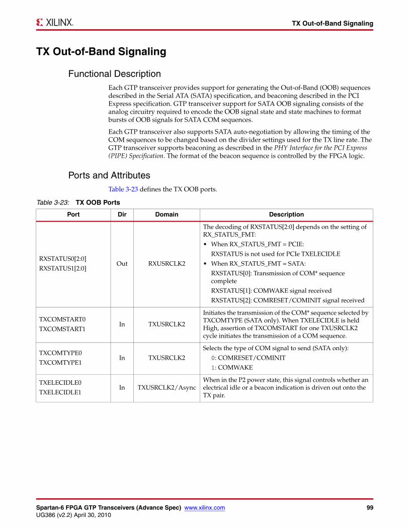
Spartan-6 FPGA GTP Transceivers (Advance Spec) www.xilinx.com 99UG386 (v2.2) April 30, 2010
TX Out-of-Band Signaling
TX Out-of-Band Signaling
Functional DescriptionEach GTP transceiver provides support for generating the Out-of-Band (OOB) sequences described in the Serial ATA (SATA) specification, and beaconing described in the PCI Express specification. GTP transceiver support for SATA OOB signaling consists of the analog circuitry required to encode the OOB signal state and state machines to format bursts of OOB signals for SATA COM sequences.
Each GTP transceiver also supports SATA auto-negotiation by allowing the timing of the COM sequences to be changed based on the divider settings used for the TX line rate. The GTP transceiver supports beaconing as described in the PHY Interface for the PCI Express (PIPE) Specification. The format of the beacon sequence is controlled by the FPGA logic.
Ports and AttributesTable 3-23 defines the TX OOB ports.
Table 3-23: TX OOB Ports
Port Dir Domain Description
RXSTATUS0[2:0]
RXSTATUS1[2:0]Out RXUSRCLK2
The decoding of RXSTATUS[2:0] depends on the setting of RX_STATUS_FMT:
• When RX_STATUS_FMT = PCIE:
RXSTATUS is not used for PCIe TXELECIDLE
• When RX_STATUS_FMT = SATA:
RXSTATUS[0]: Transmission of COM* sequence complete
RXSTATUS[1]: COMWAKE signal received
RXSTATUS[2]: COMRESET/COMINIT signal received
TXCOMSTART0
TXCOMSTART1In TXUSRCLK2
Initiates the transmission of the COM* sequence selected by TXCOMTYPE (SATA only). When TXELECIDLE is held High, assertion of TXCOMSTART for one TXUSRCLK2 cycle initiates the transmission of a COM sequence.
TXCOMTYPE0
TXCOMTYPE1In TXUSRCLK2
Selects the type of COM signal to send (SATA only):
0: COMRESET/COMINIT
1: COMWAKE
TXELECIDLE0
TXELECIDLE1In TXUSRCLK2/Async
When in the P2 power state, this signal controls whether an electrical idle or a beacon indication is driven out onto the TX pair.
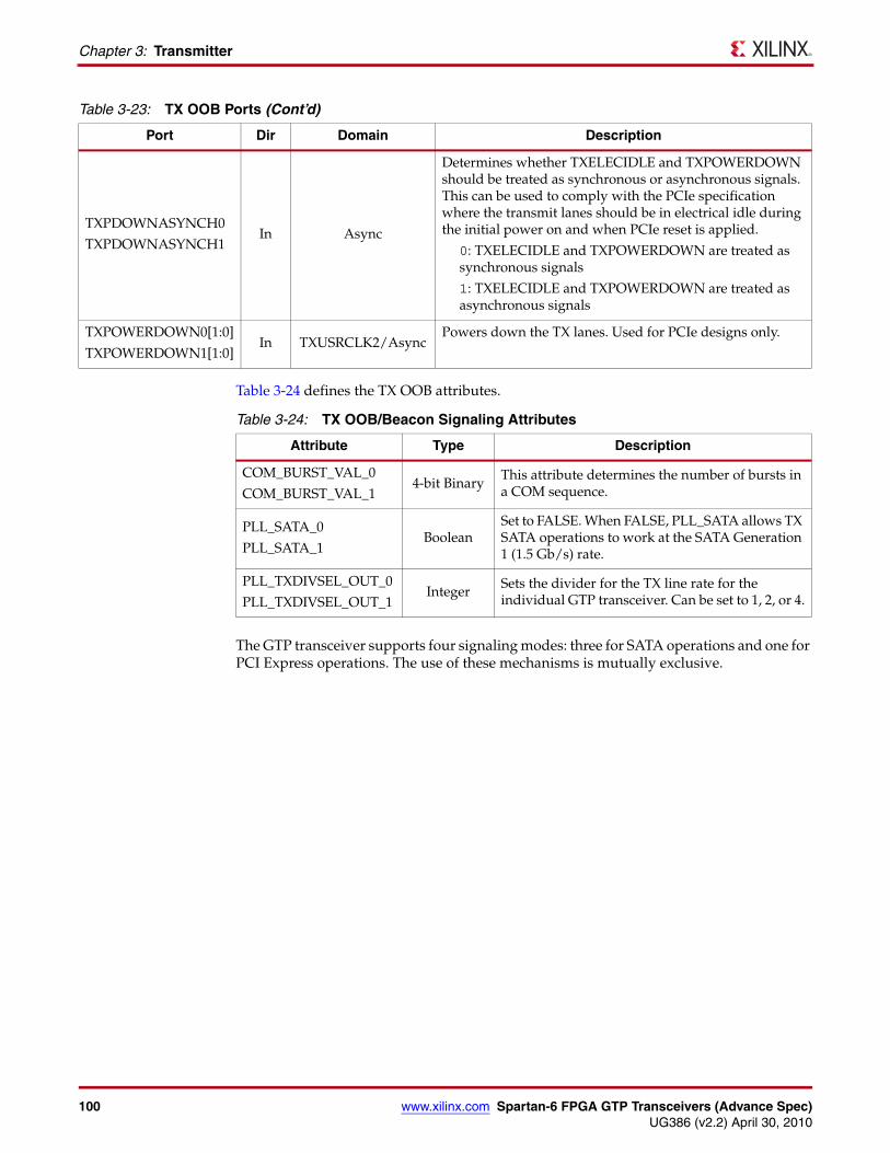
100 www.xilinx.com Spartan-6 FPGA GTP Transceivers (Advance Spec)UG386 (v2.2) April 30, 2010
Chapter 3: Transmitter
Table 3-24 defines the TX OOB attributes.
The GTP transceiver supports four signaling modes: three for SATA operations and one for PCI Express operations. The use of these mechanisms is mutually exclusive.
TXPDOWNASYNCH0
TXPDOWNASYNCH1In Async
Determines whether TXELECIDLE and TXPOWERDOWN should be treated as synchronous or asynchronous signals. This can be used to comply with the PCIe specification where the transmit lanes should be in electrical idle during the initial power on and when PCIe reset is applied.
0: TXELECIDLE and TXPOWERDOWN are treated as synchronous signals
1: TXELECIDLE and TXPOWERDOWN are treated as asynchronous signals
TXPOWERDOWN0[1:0]
TXPOWERDOWN1[1:0]In TXUSRCLK2/Async
Powers down the TX lanes. Used for PCIe designs only.
Table 3-23: TX OOB Ports (Cont’d)
Port Dir Domain Description
Table 3-24: TX OOB/Beacon Signaling Attributes
Attribute Type Description
COM_BURST_VAL_0
COM_BURST_VAL_14-bit Binary
This attribute determines the number of bursts in a COM sequence.
PLL_SATA_0
PLL_SATA_1Boolean
Set to FALSE. When FALSE, PLL_SATA allows TX SATA operations to work at the SATA Generation 1 (1.5 Gb/s) rate.
PLL_TXDIVSEL_OUT_0
PLL_TXDIVSEL_OUT_1Integer Sets the divider for the TX line rate for the
individual GTP transceiver. Can be set to 1, 2, or 4.
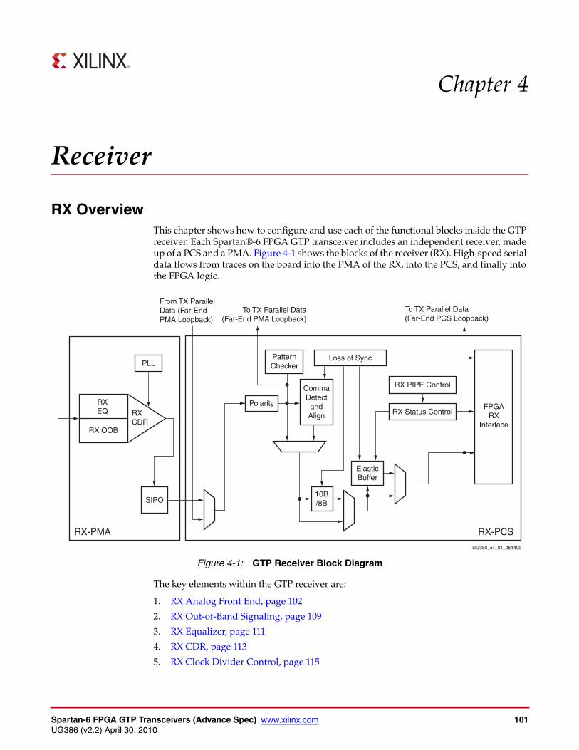
Spartan-6 FPGA GTP Transceivers (Advance Spec) www.xilinx.com 101UG386 (v2.2) April 30, 2010
Chapter 4
Receiver
RX OverviewThis chapter shows how to configure and use each of the functional blocks inside the GTP receiver. Each Spartan®-6 FPGA GTP transceiver includes an independent receiver, made up of a PCS and a PMA. Figure 4-1 shows the blocks of the receiver (RX). High-speed serial data flows from traces on the board into the PMA of the RX, into the PCS, and finally into the FPGA logic.
The key elements within the GTP receiver are:
1. RX Analog Front End, page 102
2. RX Out-of-Band Signaling, page 109
3. RX Equalizer, page 111
4. RX CDR, page 113
5. RX Clock Divider Control, page 115
X-Ref Target - Figure 4-1
Figure 4-1: GTP Receiver Block Diagram
UG386_c4_01_051409
To TX Parallel Data(Far-End PMA Loopback)
From TX ParallelData (Far-End PMA Loopback)
To TX Parallel Data(Far-End PCS Loopback)
Polarity
RX-PMA RX-PCS
FPGARX
Interface
Loss of Sync
RX PIPE Control
RX Status Control
SIPO
PLL
RXEQ
RX OOB
RXCDR
ElasticBuffer
PatternChecker
CommaDetect
andAlign
10B/8B
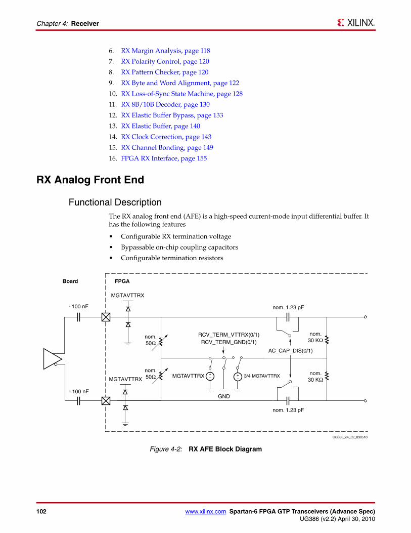
102 www.xilinx.com Spartan-6 FPGA GTP Transceivers (Advance Spec)UG386 (v2.2) April 30, 2010
Chapter 4: Receiver
6. RX Margin Analysis, page 118
7. RX Polarity Control, page 120
8. RX Pattern Checker, page 120
9. RX Byte and Word Alignment, page 122
10. RX Loss-of-Sync State Machine, page 128
11. RX 8B/10B Decoder, page 130
12. RX Elastic Buffer Bypass, page 133
13. RX Elastic Buffer, page 140
14. RX Clock Correction, page 143
15. RX Channel Bonding, page 149
16. FPGA RX Interface, page 155
RX Analog Front End
Functional DescriptionThe RX analog front end (AFE) is a high-speed current-mode input differential buffer. It has the following features
• Configurable RX termination voltage
• Bypassable on-chip coupling capacitors
• Configurable termination resistorsX-Ref Target - Figure 4-2
Figure 4-2: RX AFE Block Diagram
UG386_c4_02_030510
~100 nF
nom.50Ω
nom.50Ω
FPGABoard
MGTAVTTRX
MGTAVTTRXMGTAVTTRX
GND
RCV_TERM_VTTRX(0/1)RCV_TERM_GND(0/1)
~100 nF
AC_CAP_DIS(0/1)
nom. 1.23 pF
nom. 1.23 pF
nom.30 KΩ
nom.30 KΩ
3/4 MGTAVTTRX
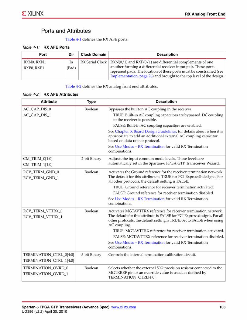
Spartan-6 FPGA GTP Transceivers (Advance Spec) www.xilinx.com 103UG386 (v2.2) April 30, 2010
RX Analog Front End
Ports and AttributesTable 4-1 defines the RX AFE ports.
Table 4-2 defines the RX analog front end attributes.
Table 4-1: RX AFE Ports
Port Dir Clock Domain Description
RXN0, RXN1
RXP0, RXP1
In
(Pad)
RX Serial Clock RXN(0/1) and RXP(0/1) are differential complements of one another forming a differential receiver input pair. These ports represent pads. The location of these ports must be constrained (see Implementation, page 26) and brought to the top level of the design.
Table 4-2: RX AFE Attributes
Attribute Type Description
AC_CAP_DIS_0
AC_CAP_DIS_1
Boolean Bypasses the built-in AC coupling in the receiver.
TRUE: Built-in AC coupling capacitors are bypassed. DC coupling to the receiver is possible.
FALSE: Built-in AC coupling capacitors are enabled.
See Chapter 5, Board Design Guidelines, for details about when it is appropriate to add an additional external AC coupling capacitor based on data rate or protocol.
See Use Modes – RX Termination for valid RX Termination combinations.
CM_TRIM_0[1:0]
CM_TRIM_1[1:0]
2-bit Binary Adjusts the input common mode levels. These levels are automatically set in the Spartan-6 FPGA GTP Transceiver Wizard.
RCV_TERM_GND_0
RCV_TERM_GND_1
Boolean Activates the Ground reference for the receiver termination network. The default for this attribute is TRUE for PCI Express® designs. For all other protocols, the default setting is FALSE.
TRUE: Ground reference for receiver termination activated.
FALSE: Ground reference for receiver termination disabled.
See Use Modes – RX Termination for valid RX Termination combinations.
RCV_TERM_VTTRX_0
RCV_TERM_VTTRX_1
Boolean Activates MGTAVTTRX reference for receiver termination network. The default for this attribute is FALSE for PCI Express designs. For all other protocols, the default setting is TRUE. Set to FALSE when using AC coupling.
TRUE: MGTAVTTRX reference for receiver termination activated.
FALSE: MGTAVTTRX reference for receiver termination disabled.
See Use Modes – RX Termination for valid RX Termination combinations.
TERMINATION_CTRL_0[4:0]
TERMINATION_CTRL_1[4:0]
5-bit Binary Controls the internal termination calibration circuit.
TERMINATION_OVRD_0
TERMINATION_OVRD_1
Boolean Selects whether the external 50Ω precision resistor connected to the MGTRREF pin or an override value is used, as defined by TERMINATION_CTRL[4:0].
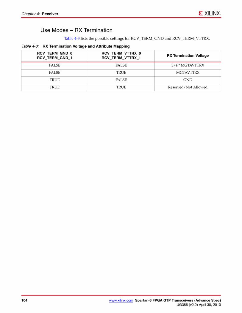
104 www.xilinx.com Spartan-6 FPGA GTP Transceivers (Advance Spec)UG386 (v2.2) April 30, 2010
Chapter 4: Receiver
Use Modes – RX TerminationTable 4-3 lists the possible settings for RCV_TERM_GND and RCV_TERM_VTTRX.
Table 4-3: RX Termination Voltage and Attribute Mapping
RCV_TERM_GND_0RCV_TERM_GND_1
RCV_TERM_VTTRX_0RCV_TERM_VTTRX_1
RX Termination Voltage
FALSE FALSE 3/4 * MGTAVTTRX
FALSE TRUE MGTAVTTRX
TRUE FALSE GND
TRUE TRUE Reserved/Not Allowed
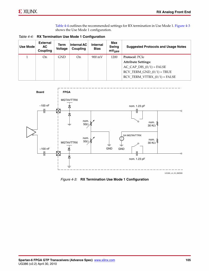
Spartan-6 FPGA GTP Transceivers (Advance Spec) www.xilinx.com 105UG386 (v2.2) April 30, 2010
RX Analog Front End
Table 4-4 outlines the recommended settings for RX termination in Use Mode 1. Figure 4-3 shows the Use Mode 1 configuration.
Table 4-4: RX Termination Use Mode 1 Configuration
Use ModeExternal
AC Coupling
Term Voltage
Internal AC Coupling
Internal Bias
Max SwingmVDPP
Suggested Protocols and Usage Notes
1 On GND On 900 mV 1200 Protocol: PCIe
Attribute Settings:
AC_CAP_DIS_(0/1) = FALSE
RCV_TERM_GND_(0/1) = TRUE
RCV_TERM_VTTRX_(0/1) = FALSE
X-Ref Target - Figure 4-3
Figure 4-3: RX Termination Use Mode 1 Configuration
UG386_c4_03_092509
~100 nF
nom.50Ω
nom.50Ω
FPGABoard
MGTAVTTRX
MGTAVTTRX
GND~100 nF
nom. 1.23 pF
nom. 1.23 pF
nom.30 KΩ
nom.30 KΩ
GND
3/4 MGTAVTTRX
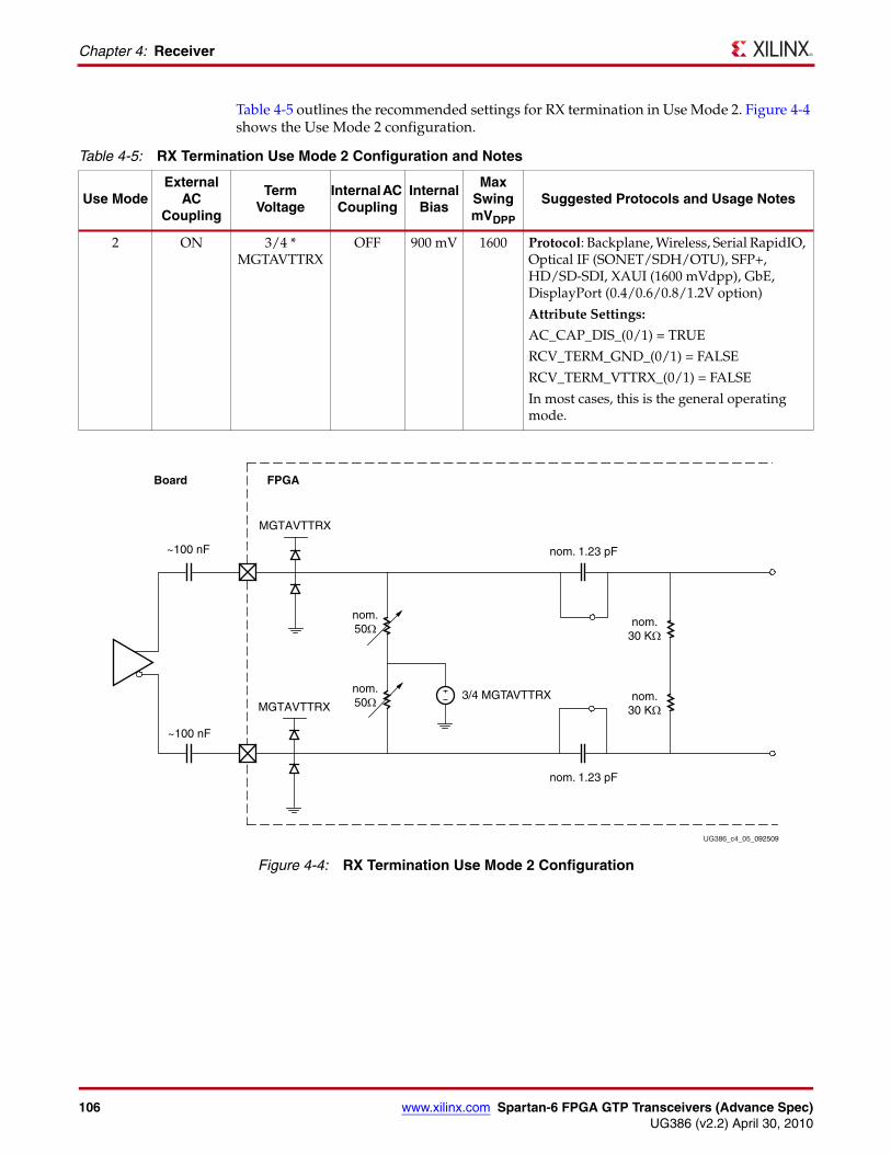
106 www.xilinx.com Spartan-6 FPGA GTP Transceivers (Advance Spec)UG386 (v2.2) April 30, 2010
Chapter 4: Receiver
Table 4-5 outlines the recommended settings for RX termination in Use Mode 2. Figure 4-4 shows the Use Mode 2 configuration.
Table 4-5: RX Termination Use Mode 2 Configuration and Notes
Use ModeExternal
AC Coupling
TermVoltage
Internal AC Coupling
Internal Bias
Max SwingmVDPP
Suggested Protocols and Usage Notes
2 ON 3/4 * MGTAVTTRX
OFF 900 mV 1600 Protocol: Backplane, Wireless, Serial RapidIO, Optical IF (SONET/SDH/OTU), SFP+, HD/SD-SDI, XAUI (1600 mVdpp), GbE, DisplayPort (0.4/0.6/0.8/1.2V option)
Attribute Settings:
AC_CAP_DIS_(0/1) = TRUE
RCV_TERM_GND_(0/1) = FALSE
RCV_TERM_VTTRX_(0/1) = FALSE
In most cases, this is the general operating mode.
X-Ref Target - Figure 4-4
Figure 4-4: RX Termination Use Mode 2 Configuration
UG386_c4_05_092509
~100 nF
nom.50Ω
nom.50Ω
FPGABoard
MGTAVTTRX
MGTAVTTRX
~100 nF
nom. 1.23 pF
nom. 1.23 pF
nom.30 KΩ
nom.30 KΩ
3/4 MGTAVTTRX
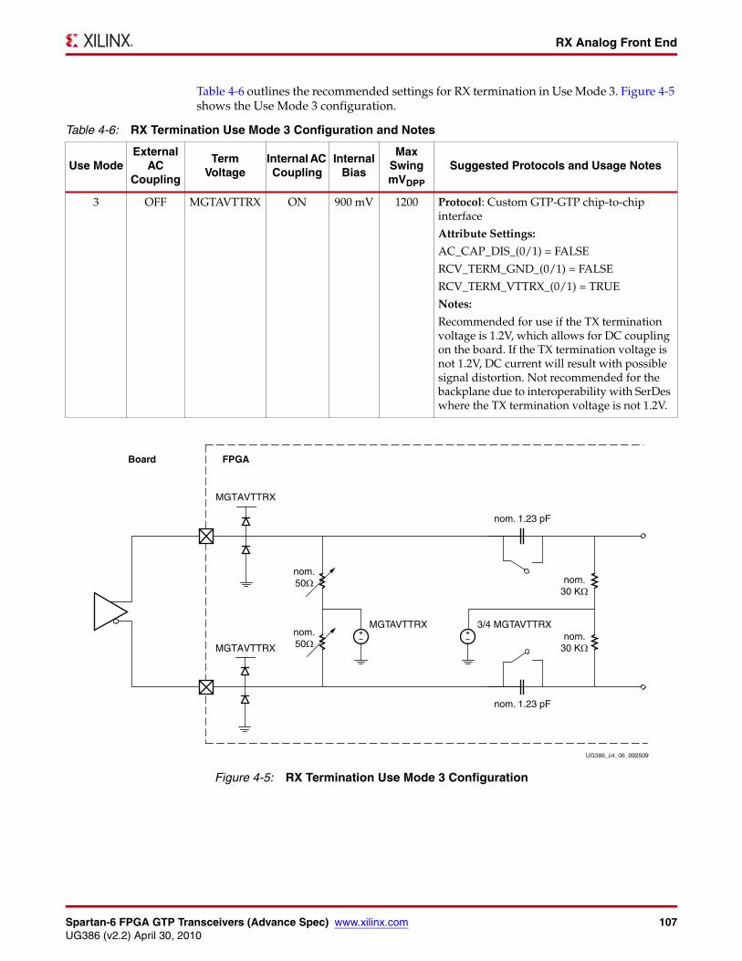
Spartan-6 FPGA GTP Transceivers (Advance Spec) www.xilinx.com 107UG386 (v2.2) April 30, 2010
RX Analog Front End
Table 4-6 outlines the recommended settings for RX termination in Use Mode 3. Figure 4-5 shows the Use Mode 3 configuration.
Table 4-6: RX Termination Use Mode 3 Configuration and Notes
Use ModeExternal
AC Coupling
TermVoltage
Internal AC Coupling
Internal Bias
Max SwingmVDPP
Suggested Protocols and Usage Notes
3 OFF MGTAVTTRX ON 900 mV 1200 Protocol: Custom GTP-GTP chip-to-chip interface
Attribute Settings:
AC_CAP_DIS_(0/1) = FALSE
RCV_TERM_GND_(0/1) = FALSE
RCV_TERM_VTTRX_(0/1) = TRUE
Notes:
Recommended for use if the TX termination voltage is 1.2V, which allows for DC coupling on the board. If the TX termination voltage is not 1.2V, DC current will result with possible signal distortion. Not recommended for the backplane due to interoperability with SerDes where the TX termination voltage is not 1.2V.
X-Ref Target - Figure 4-5
Figure 4-5: RX Termination Use Mode 3 Configuration
UG386_c4_06_092509
nom.50Ω
nom.50Ω
FPGABoard
MGTAVTTRX
MGTAVTTRX
nom. 1.23 pF
nom. 1.23 pF
nom.30 KΩ
nom.30 KΩ
MGTAVTTRX 3/4 MGTAVTTRX
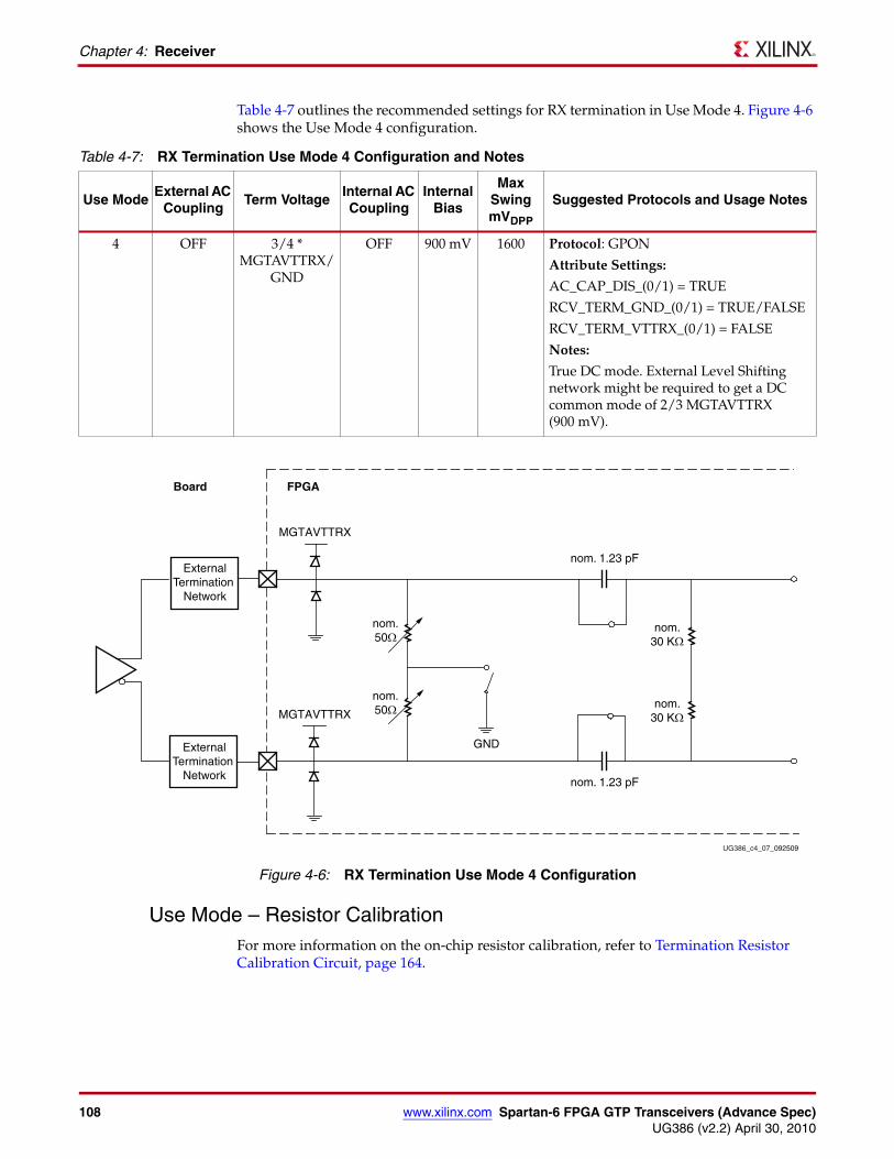
108 www.xilinx.com Spartan-6 FPGA GTP Transceivers (Advance Spec)UG386 (v2.2) April 30, 2010
Chapter 4: Receiver
Table 4-7 outlines the recommended settings for RX termination in Use Mode 4. Figure 4-6 shows the Use Mode 4 configuration.
Use Mode – Resistor CalibrationFor more information on the on-chip resistor calibration, refer to Termination Resistor Calibration Circuit, page 164.
Table 4-7: RX Termination Use Mode 4 Configuration and Notes
Use ModeExternal AC
CouplingTerm Voltage
Internal AC Coupling
Internal Bias
Max SwingmVDPP
Suggested Protocols and Usage Notes
4 OFF 3/4 *MGTAVTTRX/
GND
OFF 900 mV 1600 Protocol: GPON
Attribute Settings:
AC_CAP_DIS_(0/1) = TRUE
RCV_TERM_GND_(0/1) = TRUE/FALSE
RCV_TERM_VTTRX_(0/1) = FALSE
Notes:
True DC mode. External Level Shifting network might be required to get a DC common mode of 2/3 MGTAVTTRX (900 mV).
X-Ref Target - Figure 4-6
Figure 4-6: RX Termination Use Mode 4 Configuration
UG386_c4_07_092509
nom.50Ω
nom.50Ω
FPGABoard
MGTAVTTRX
MGTAVTTRX
nom. 1.23 pF
nom. 1.23 pF
nom.30 KΩ
nom.30 KΩ
ExternalTermination
Network
ExternalTermination
Network
GND
Spartan-6 FPGA GTP Transceivers (Advance Spec) www.xilinx.com 109UG386 (v2.2) April 30, 2010
RX Out-of-Band Signaling
RX Out-of-Band Signaling
Functional DescriptionThe GTP receiver provides support for decoding the Out-of-Band (OOB) sequences described in the Serial ATA (SATA) specification and supports beaconing described in the PCI Express specification. GTP receiver support for SATA OOB signaling consists of the analog circuitry required to decode the OOB signal state and state machines to decode bursts of OOB signals for SATA COM sequences.
The GTP receiver also supports beacons that are PCI Express compliant by using interface signals defined in the PHY Interface for the PCI Express (PIPE) Specification. The FPGA logic decodes the beacon sequence.
Ports and AttributesTable 4-8 defines the RX OOB ports.
Table 4-9 defines the RX OOB attributes.
Table 4-8: RX OOB Ports
Port Dir Clock Domain Description
RXELECIDLE0
RXELECIDLE1
Out Async Indicates the differential voltage between RXN and RXP dropped below the minimum threshold (OOBDETECT_THRESHOLD). Signals below this threshold are OOB signals.
1: OOB signal detected. The differential voltage is below the minimum threshold.
0: OOB signal not detected. The differential voltage is above the minimum threshold.
This port is intended for PCI Express and SATA standards.
RXSTATUS0[2:0]
RXSTATUS1[2:0]
Out RXUSRCLK2 RXSTATUS[2:0] are used only for PCIe® mode, as defined by the PIPE specification.
RXVALID0
RXVALID1
Out RXUSRCLK2 Indicates symbol lock and valid data on RXDATA and RXCHARISK[3:0] when High, as defined in the PIPE specification.
Table 4-9: RX OOB Attributes
Attribute Type Description
OOB_CLK_DIVIDER_0
OOB_CLK_DIVIDER_1
Integer Sets the squelch clock rate. The squelch clock must be set between 25 MHz and 37.5 MHz, as close to 25 MHz as possible for the SATA OOB detector to work correctly.
Squelch Clock rate = CLKIN/OOB_CLK_DIVIDER
Valid divider settings are 1, 2, 4, 6, 8, 10, 12, and 14.
110 www.xilinx.com Spartan-6 FPGA GTP Transceivers (Advance Spec)UG386 (v2.2) April 30, 2010
Chapter 4: Receiver
OOBDETECT_THRESHOLD_0
OOBDETECT_THRESHOLD_1
3-bit Binary Sets the minimum differential voltage between RXN and RXP. When the differential voltage drops below this level, the incoming signal is considered an OOB signal. This 3-bit binary encoded attribute has the following nominal values of the OOB threshold voltage(1):
Value OOB Nominal Threshold Voltage (mV)
000 – 101 Not supported
110 (default) 105
111 115
RX_STATUS_FMT_0
RX_STATUS_FMT_1
String Defines which status encoding is used:
PCIE: PCI Express encoding
SATA: SATA encoding
SATA_BURST_VAL_0
SATA_BURST_VAL_1
3-bit Binary Number of bursts required to declare a COM match. The default for SATA_BURST_VAL is 4, which is the burst count specified in SATA for COMINIT, COMRESET, and COMWAIT.
SATA_IDLE_VAL_0
SATA_IDLE_VAL_1
3-bit Binary Number of idles required to declare a COM match. Each idle is an OOB signal with a length that matches either COMINIT/COMRESET or COMWAIT. When the SATA detector starts to count one type of idle (for example, COMRESET/COMINIT), it resets the count if it receives the other type. This value defaults to 3 to match the SATA specification.
SATA_MAX_BURST_0
SATA_MAX_BURST_1
Integer Sets the threshold for the SATA detector to reject a burst in terms of squelch clock cycles. SATA_MAX_BURST has valid values between 1 and 61 (the default is 7) and must be greater than SATA_MIN_BURST.
SATA_MAX_INIT_0
SATA_MAX_INIT_1
Integer Sets the maximum time allowed for a COMINIT/COMRESET idle for the SATA detector in terms of squelch clock cycles. SATA_MAX_INIT has valid values between 1 and 61 (the default is 22) and must be greater than SATA_MIN_INIT.
SATA_MAX_WAKE_0
SATA_MAX_WAKE_1
Integer Sets the maximum time allowed for a COMWAKE idle for the SATA detector in terms of squelch clock cycles. SATA_MAX_WAKE has valid values between 1 and 61 (the default is 7) and must be greater than SATA_MIN_WAKE.
SATA_MIN_BURST_0
SATA_MIN_BURST_1
Integer Sets the threshold for the SATA detector to reject a burst in terms of squelch clock cycles. SATA_MIN_BURST has valid values between 1 and 61 (the default is 4) and must be less than SATA_MAX_BURST.
SATA_MIN_INIT_0
SATA_MIN_INIT_1
Integer In SATA, OOB signals are used as idles in COMINIT, COMRESET, and COMWAKE. The minimum length of an idle that must be accepted for COMINIT/COMRESET signals in SATA is 304 ns. If the idle is shorter than 175 ns, it cannot be used for COMINIT/COMRESET. SATA_MIN_INIT is used to set the minimum time allowed for a COMINIT/COMRESET Idle for the SATA detector in terms of squelch clock cycles.
SATA_MIN_INIT has valid values between 1 and 61 (the default is 12) and must be less than SATA_MAX_INIT. The squelch clock is set based using OOB_CLK_DIVIDER.
Table 4-9: RX OOB Attributes (Cont’d)
Attribute Type Description
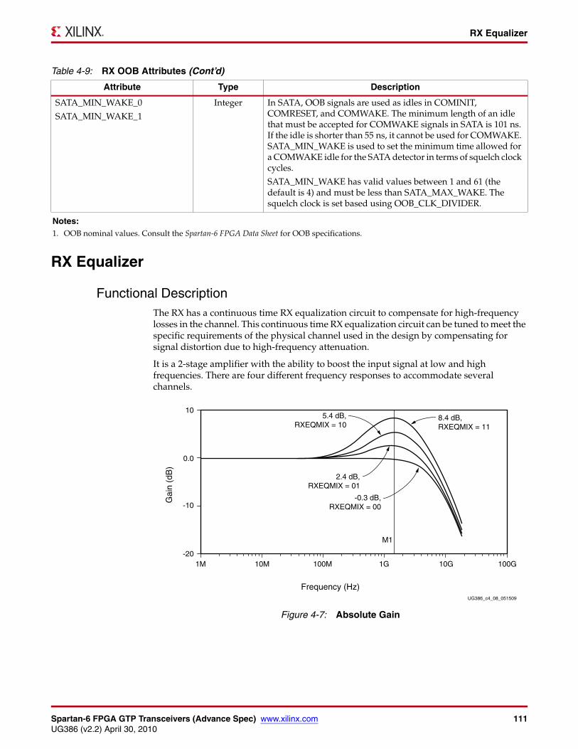
Spartan-6 FPGA GTP Transceivers (Advance Spec) www.xilinx.com 111UG386 (v2.2) April 30, 2010
RX Equalizer
RX Equalizer
Functional DescriptionThe RX has a continuous time RX equalization circuit to compensate for high-frequency losses in the channel. This continuous time RX equalization circuit can be tuned to meet the specific requirements of the physical channel used in the design by compensating for signal distortion due to high-frequency attenuation.
It is a 2-stage amplifier with the ability to boost the input signal at low and high frequencies. There are four different frequency responses to accommodate several channels.
SATA_MIN_WAKE_0
SATA_MIN_WAKE_1
Integer In SATA, OOB signals are used as idles in COMINIT, COMRESET, and COMWAKE. The minimum length of an idle that must be accepted for COMWAKE signals in SATA is 101 ns. If the idle is shorter than 55 ns, it cannot be used for COMWAKE. SATA_MIN_WAKE is used to set the minimum time allowed for a COMWAKE idle for the SATA detector in terms of squelch clock cycles.
SATA_MIN_WAKE has valid values between 1 and 61 (the default is 4) and must be less than SATA_MAX_WAKE. The squelch clock is set based using OOB_CLK_DIVIDER.
Notes: 1. OOB nominal values. Consult the Spartan-6 FPGA Data Sheet for OOB specifications.
Table 4-9: RX OOB Attributes (Cont’d)
Attribute Type Description
X-Ref Target - Figure 4-7
Figure 4-7: Absolute Gain
-20
-10
0.0
10
1M 10M 100M
8.4 dB,RXEQMIX = 11
5.4 dB,RXEQMIX = 10
2.4 dB,RXEQMIX = 01
-0.3 dB,RXEQMIX = 00
1G
M1
10G 100G
Frequency (Hz)
Gai
n (d
B)
UG386_c4_08_051509
112 www.xilinx.com Spartan-6 FPGA GTP Transceivers (Advance Spec)UG386 (v2.2) April 30, 2010
Chapter 4: Receiver
Ports and AttributesTable 4-10 defines the RX equalization ports.
Table 4-11 defines the RX equalization attributes.
Use Mode – Continuous Time RX Linear EqualizerModes with greater gain at high frequencies are intended for lossy (usually longer) channels. A simple way to determine how to use the RX equalizer follows:
1. Determine the operating data rate.
2. Determine the channel loss (board) in dB at data rate/2. This is the differential insertion loss from measured or extracted S-parameter data commonly referred to as Sdd21.
3. Pick the appropriate RXEQMIX setting from the gain plot.
The appropriate setting of RXEQMIX can be picked based on these results.
These settings must always be verified in hardware because there are several considerations, such as discontinuities in the system, jitter on the TX clocks, which cannot be compensated for by the linear equalizer.
ExampleData Rate = 3.125 Gb/s, which means the fundamental frequency is 1.5625 GHz.Channel Loss in dB at 1.5625 GHz = 6 dB.RXEQMIX[1:0] = 10.This setting allows compensation of 6 dB at 1.5625 GHz hence providing the needed gain.
Table 4-10: RX Equalization Ports
Port DirClock
DomainDescription
RXEQMIX0[1:0]
RXEQMIX1[1:0]
In Async Receiver Equalization Control. The default is 2’b00, user specific.
RXEQMIX[1:0] Gain (dB)(1)
00 –0.3
01 2.6
10 5.4
11 8.4
Notes: 1. Nominal values. Refer to the Spartan-6 FPGA Data Sheet for the exact values based on marginal
conditions.
Table 4-11: RX Equalization Attributes
Attribute Type Description
RXEQ_CFG_0[7:0]
RXEQ_CFG_1[7:0]
8-bit Binary RXEQ_CFG_0
RXEQ_CFG_1
Description
[7:3] Limiter/EQAMP gain and power control
[2:0] ISOAMP gain and power control
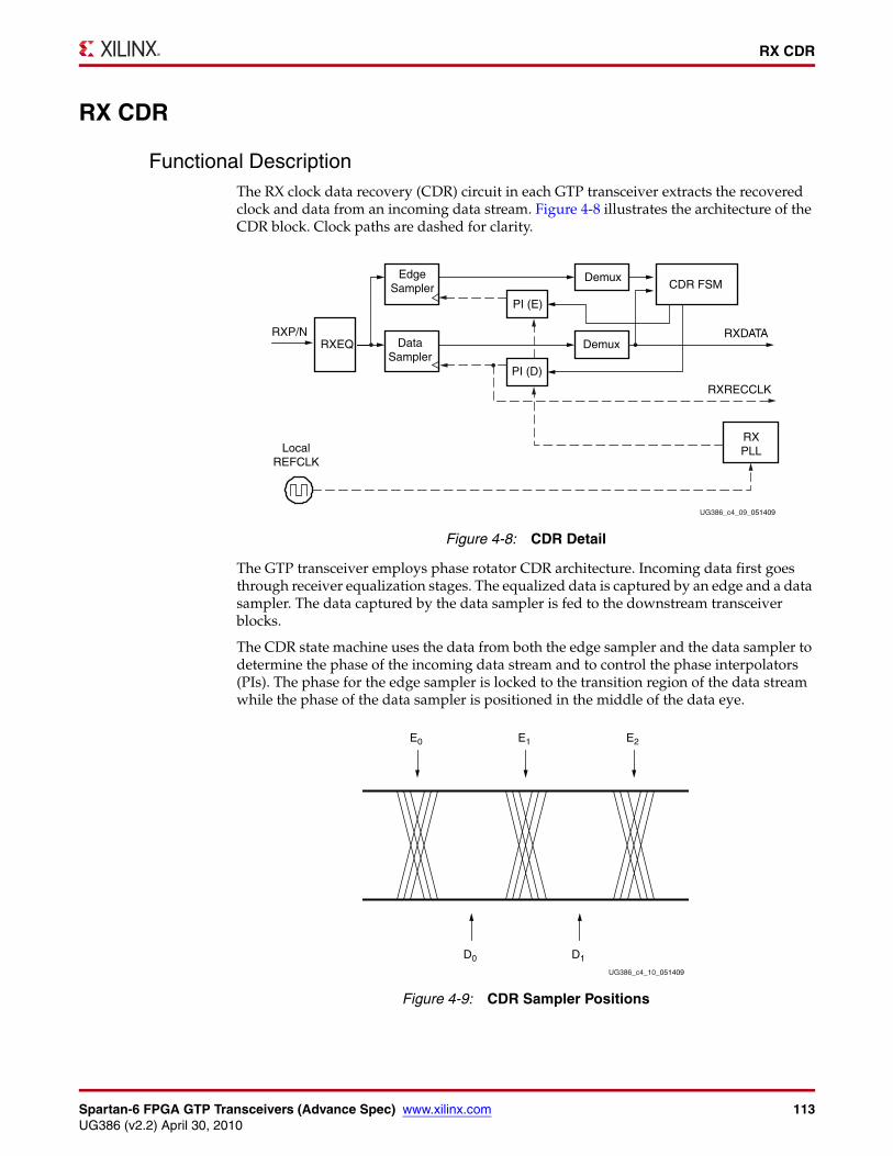
Spartan-6 FPGA GTP Transceivers (Advance Spec) www.xilinx.com 113UG386 (v2.2) April 30, 2010
RX CDR
RX CDR
Functional DescriptionThe RX clock data recovery (CDR) circuit in each GTP transceiver extracts the recovered clock and data from an incoming data stream. Figure 4-8 illustrates the architecture of the CDR block. Clock paths are dashed for clarity.
The GTP transceiver employs phase rotator CDR architecture. Incoming data first goes through receiver equalization stages. The equalized data is captured by an edge and a data sampler. The data captured by the data sampler is fed to the downstream transceiver blocks.
The CDR state machine uses the data from both the edge sampler and the data sampler to determine the phase of the incoming data stream and to control the phase interpolators (PIs). The phase for the edge sampler is locked to the transition region of the data stream while the phase of the data sampler is positioned in the middle of the data eye.
X-Ref Target - Figure 4-8
Figure 4-8: CDR Detail
X-Ref Target - Figure 4-9
Figure 4-9: CDR Sampler Positions
UG386_c4_09_051409
EdgeSampler
DemuxCDR FSM
DataSampler
RXP/NRXEQ
LocalREFCLK
PI (E)
PI (D)
RXPLL
RXDATA
RXRECCLK
Demux
UG386_c4_10_051409
E0 E1 E2
D0 D1
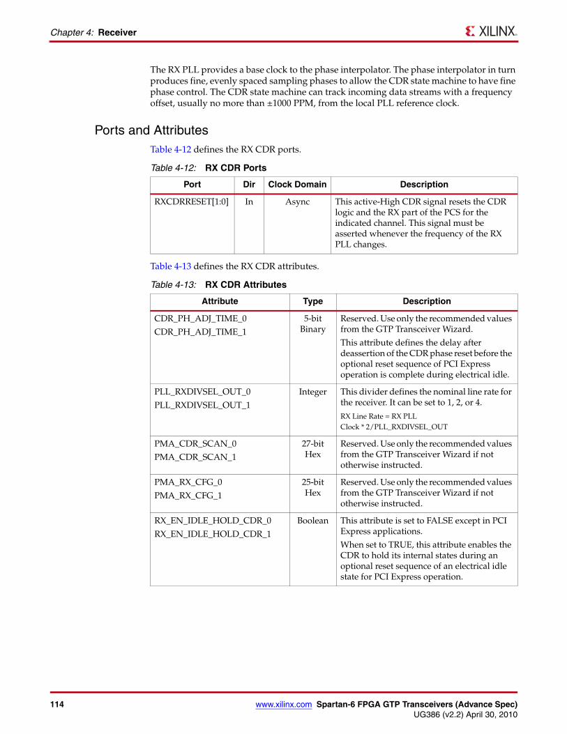
114 www.xilinx.com Spartan-6 FPGA GTP Transceivers (Advance Spec)UG386 (v2.2) April 30, 2010
Chapter 4: Receiver
The RX PLL provides a base clock to the phase interpolator. The phase interpolator in turn produces fine, evenly spaced sampling phases to allow the CDR state machine to have fine phase control. The CDR state machine can track incoming data streams with a frequency offset, usually no more than ±1000 PPM, from the local PLL reference clock.
Ports and AttributesTable 4-12 defines the RX CDR ports.
Table 4-13 defines the RX CDR attributes.
Table 4-12: RX CDR Ports
Port Dir Clock Domain Description
RXCDRRESET[1:0] In Async This active-High CDR signal resets the CDR logic and the RX part of the PCS for the indicated channel. This signal must be asserted whenever the frequency of the RX PLL changes.
Table 4-13: RX CDR Attributes
Attribute Type Description
CDR_PH_ADJ_TIME_0
CDR_PH_ADJ_TIME_1
5-bit Binary
Reserved. Use only the recommended values from the GTP Transceiver Wizard.
This attribute defines the delay after deassertion of the CDR phase reset before the optional reset sequence of PCI Express operation is complete during electrical idle.
PLL_RXDIVSEL_OUT_0
PLL_RXDIVSEL_OUT_1
Integer This divider defines the nominal line rate for the receiver. It can be set to 1, 2, or 4.
RX Line Rate = RX PLL Clock * 2/PLL_RXDIVSEL_OUT
PMA_CDR_SCAN_0
PMA_CDR_SCAN_1
27-bit Hex
Reserved. Use only the recommended values from the GTP Transceiver Wizard if not otherwise instructed.
PMA_RX_CFG_0
PMA_RX_CFG_1
25-bit Hex
Reserved. Use only the recommended values from the GTP Transceiver Wizard if not otherwise instructed.
RX_EN_IDLE_HOLD_CDR_0
RX_EN_IDLE_HOLD_CDR_1
Boolean This attribute is set to FALSE except in PCI Express applications.
When set to TRUE, this attribute enables the CDR to hold its internal states during an optional reset sequence of an electrical idle state for PCI Express operation.
Spartan-6 FPGA GTP Transceivers (Advance Spec) www.xilinx.com 115UG386 (v2.2) April 30, 2010
RX Clock Divider Control
RX Clock Divider Control
Functional DescriptionThe RX clock divider control block has two main components: serial clock divider control and parallel clock divider control. The clock divider details for the GTP0 transceiver are illustrated in Figure 4-10. The GTP1 transceiver has an identical structure.
RX_EN_IDLE_RESET_FR_0
RX_EN_IDLE_RESET_FR_1
Boolean This attribute is set to FALSE except in PCI Express applications.
When set to TRUE, this attribute enables an automatic reset of the CDR frequency during an optional reset sequence of an electrical idle state for PCI Express operation.
RX_EN_IDLE_RESET_PH_0
RX_EN_IDLE_RESET_PH_1
Boolean This attribute is set to FALSE except in PCI Express applications.
When set to TRUE, this attribute enables an automatic reset of the CDR phase during an optional reset sequence of an electrical idle state for PCI Express operation.
Table 4-13: RX CDR Attributes (Cont’d)
Attribute Type Description
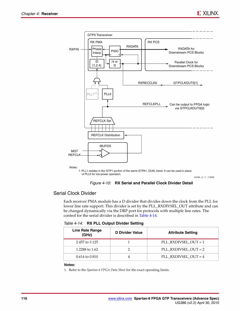
116 www.xilinx.com Spartan-6 FPGA GTP Transceivers (Advance Spec)UG386 (v2.2) April 30, 2010
Chapter 4: Receiver
Serial Clock Divider
Each receiver PMA module has a D divider that divides down the clock from the PLL for lower line rate support. This divider is set by the PLL_RXDIVSEL_OUT attribute and can be changed dynamically via the DRP port for protocols with multiple line rates. The control for the serial divider is described in Table 4-14.
X-Ref Target - Figure 4-10
Figure 4-10: RX Serial and Parallel Clock Divider Detail
UG386_c4_11_110309
RX PMA RX PCS
GTPCLKOUT0[1]
RXDATA
PISO
REFCLK Distribution
O
REFCLK Sel
Notes: 1. PLL1 resides in the GTP1 portion of the same GTPA1_DUAL block. It can be used in place of PLL0 for low-power operation.
GTP0 Transceiver
RXP/N PhaseInterp
RXDATA forDownstream PCS Blocks
Parallel Clock forDownstream PCS Blocks
/4 or/5
/D{1,2,4}
RXRECCLK0
REFCLKPLL Can be output to FPGA logicvia GTPCLKOUT0[0]
PLL0PLL1(1)
IBUFDS
MGTREFCLK
Table 4-14: RX PLL Output Divider Setting
Line Rate Range(GHz)
D Divider Value Attribute Setting
2.457 to 3.125 1 PLL_RXDIVSEL_OUT = 1
1.2288 to 1.62 2 PLL_RXDIVSEL_OUT = 2
0.614 to 0.810 4 PLL_RXDIVSEL_OUT = 4
Notes: 1. Refer to the Spartan-6 FPGA Data Sheet for the exact operating limits.
Spartan-6 FPGA GTP Transceivers (Advance Spec) www.xilinx.com 117UG386 (v2.2) April 30, 2010
RX Clock Divider Control
Parallel Clock Divider
The recovered clock can be brought out to the FPGA logic. The recovered clock is used by protocols that do not have a clock compensation mechanism and require the use of a clock synchronous to the data, the recovered clock, to clock the downstream FPGA logic. The receive parallel clock divider block outputs a 1-byte data width recovered clock to the FPGA logic via the signal port GTPCLKOUT[1]. The frequency is line rate divided by 8 or 10 depending on the value of INTDATAWIDTH.
Ports and AttributesTable 4-15 defines the RX clock divider control ports.
Table 4-16 defines the RX CDR attributes.
Table 4-15: RX Clock Divider Control Ports
Port Dir Clock Domain Description
GTPCLKOUT0[1:0]
GTPCLKOUT1[1:0]
Out N/A GTPCLKOUT(0/1) is the recommended signal port to bring clocks inside the GTPA1_DUAL tile to the FPGA logic.
Bit 0 of GTPCLKOUT(0/1) allows the user to output either TXOUTCLK(0/1) or REFCLKPLL(0/1). CLK_OUT_GTP_SEL_(0/1) selects the clock to be output.
Bit 1 of GTPCLKOUT(0/1) outputs RXRECCLK(0/1).
INTDATAWIDTH0
INTDATAWIDTH1
In Async This port specifies the width of the internal datapath and the value of the parallel clock divider for both the TX and the RX datapaths of the same GTP lane.
0: Internal datapath is 8 bits wide and the parallel clock divider is set to 4.
1: Internal datapath is 10 bits wide and the parallel clock divider is set to 5.
Because INTDATAWIDTH also controls the PLL feedback divider N1, when a PLL is shared between the two lanes within the GTPA1_DUAL tile, the INTDATAWIDTH ports in both lanes must be set to the same value.
RXRECCLK0
RXRECCLK1
Out N/A Reserved. GTPCLKOUT(0/1)[1] should be used instead.
Table 4-16: RX CDR Attributes
Attribute Type Description
PLL_RXDIVSEL_OUT Integer This attribute controls the setting for the RX serial clock divider for low line rate support (See Table 4-14, page 116.
Valid settings are:
1: Set D divider to 1
2: Set D divider to 2
4: Set D divider to 4
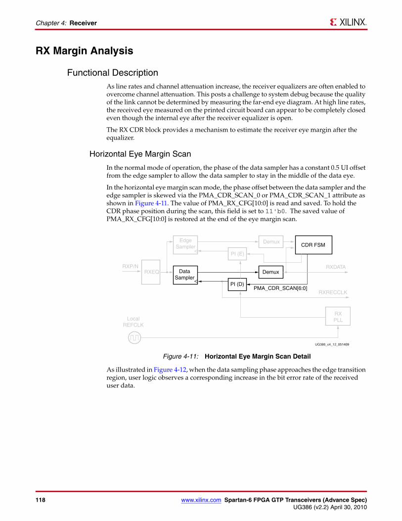
118 www.xilinx.com Spartan-6 FPGA GTP Transceivers (Advance Spec)UG386 (v2.2) April 30, 2010
Chapter 4: Receiver
RX Margin Analysis
Functional DescriptionAs line rates and channel attenuation increase, the receiver equalizers are often enabled to overcome channel attenuation. This posts a challenge to system debug because the quality of the link cannot be determined by measuring the far-end eye diagram. At high line rates, the received eye measured on the printed circuit board can appear to be completely closed even though the internal eye after the receiver equalizer is open.
The RX CDR block provides a mechanism to estimate the receiver eye margin after the equalizer.
Horizontal Eye Margin Scan
In the normal mode of operation, the phase of the data sampler has a constant 0.5 UI offset from the edge sampler to allow the data sampler to stay in the middle of the data eye.
In the horizontal eye margin scan mode, the phase offset between the data sampler and the edge sampler is skewed via the PMA_CDR_SCAN_0 or PMA_CDR_SCAN_1 attribute as shown in Figure 4-11. The value of PMA_RX_CFG[10:0] is read and saved. To hold the CDR phase position during the scan, this field is set to 11'b0. The saved value of PMA_RX_CFG[10:0] is restored at the end of the eye margin scan.
As illustrated in Figure 4-12, when the data sampling phase approaches the edge transition region, user logic observes a corresponding increase in the bit error rate of the received user data.
X-Ref Target - Figure 4-11
Figure 4-11: Horizontal Eye Margin Scan Detail
UG386_c4_12_051409
EdgeSampler
DemuxCDR FSM
DataSampler
RXP/NRXEQ
LocalREFCLK
PI (E)
PI (D)
RXPLL
RXDATA
RXRECCLK
Demux
PMA_CDR_SCAN[6:0]
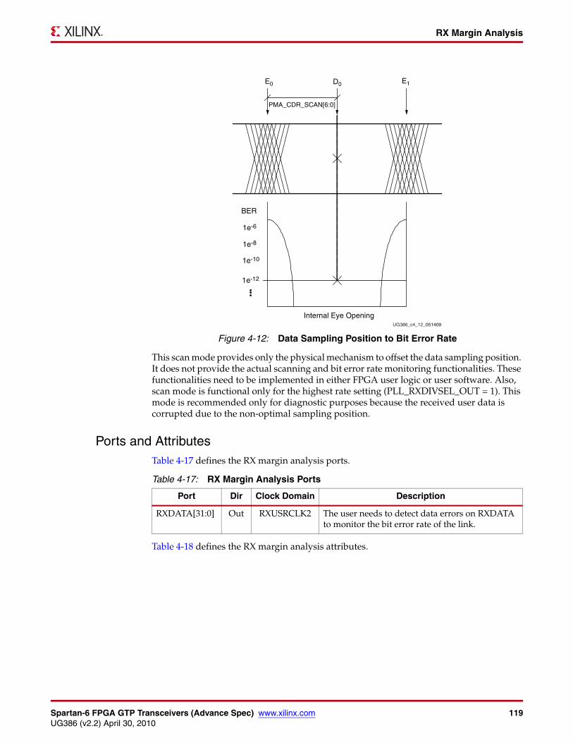
Spartan-6 FPGA GTP Transceivers (Advance Spec) www.xilinx.com 119UG386 (v2.2) April 30, 2010
RX Margin Analysis
This scan mode provides only the physical mechanism to offset the data sampling position. It does not provide the actual scanning and bit error rate monitoring functionalities. These functionalities need to be implemented in either FPGA user logic or user software. Also, scan mode is functional only for the highest rate setting (PLL_RXDIVSEL_OUT = 1). This mode is recommended only for diagnostic purposes because the received user data is corrupted due to the non-optimal sampling position.
Ports and AttributesTable 4-17 defines the RX margin analysis ports.
Table 4-18 defines the RX margin analysis attributes.
X-Ref Target - Figure 4-12
Figure 4-12: Data Sampling Position to Bit Error Rate
UG386_c4_12_051409
Internal Eye Opening
BER
E0 D0 E1
PMA_CDR_SCAN[6:0]
1e-6
1e-8
1e-10
1e-12
Table 4-17: RX Margin Analysis Ports
Port Dir Clock Domain Description
RXDATA[31:0] Out RXUSRCLK2 The user needs to detect data errors on RXDATA to monitor the bit error rate of the link.
120 www.xilinx.com Spartan-6 FPGA GTP Transceivers (Advance Spec)UG386 (v2.2) April 30, 2010
Chapter 4: Receiver
RX Polarity Control
Functional DescriptionThe GTP RX can invert incoming data using the RX polarity control function. This function is useful in designs where the RXP and RXN signals can be accidentally connected in reverse. The RXPOLARITY port is driven High to invert the polarity of incoming data.
Ports and AttributesTable 4-19 defines the RX polarity control ports.
There are no RX polarity control attributes.
Using RX Polarity ControlIf the polarity of RXP/RXN needs to be inverted, RXPOLARITY must be tied High.
RX Pattern Checker
Functional DescriptionThe GTP receiver includes a built-in PRBS checker. This checker can be set to check for one of four industry-standard PRBS patterns. The checker is self-synchronizing and works on
Table 4-18: RX Margin Analysis Attributes
Attribute Type Description
PMA_CDR_SCAN_0[26:0]
PMA_CDR_SCAN_1[26:0]
27-bit Hex
This field allows direct control of the CDR sampling point. Varying bits 7 to 0 from 8’h00 to 8’h7F (0 to 127 decimal) moves the sampling point from the left edge to the right edge of the unit interval. Bit 7 is always set to zero. Bits 26 to 8 are reserved and must be left at the recommended values from the GTP Transceiver Wizard.
PMA_RX_CFG_0[24:0]
PMA_RX_CFG_1[24:0]
25-bit Hex
Bits 10 to 0 should be set to zero to maintain the CDR position during the eye margin scan. Bits 25 to 11 are reserved and must be left at the recommended values from the GTP Transceiver Wizard.
Table 4-19: RX Polarity Control Ports
Port Dir Clock Domain Description
RXPOLARITY0
RXPOLARITY1
In RXUSRCLK2 The RX polarity port can invert the polarity of incoming data.
0: Not inverted. RXP is positive and RXN is negative.
1: Inverted. RXP is negative and RXN is positive.
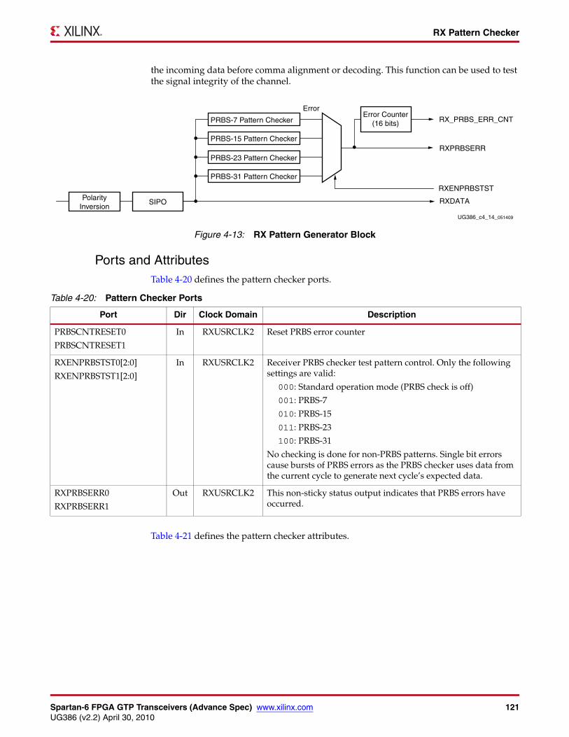
Spartan-6 FPGA GTP Transceivers (Advance Spec) www.xilinx.com 121UG386 (v2.2) April 30, 2010
RX Pattern Checker
the incoming data before comma alignment or decoding. This function can be used to test the signal integrity of the channel.
Ports and AttributesTable 4-20 defines the pattern checker ports.
Table 4-21 defines the pattern checker attributes.
X-Ref Target - Figure 4-13
Figure 4-13: RX Pattern Generator Block
RXDATA
RXENPRBSTST
Error
UG386_c4_14_051409
PolarityInversion
SIPO
PRBS-7 Pattern Checker
PRBS-15 Pattern Checker
PRBS-23 Pattern Checker
PRBS-31 Pattern Checker
Error Counter(16 bits) RX_PRBS_ERR_CNT
RXPRBSERR
Table 4-20: Pattern Checker Ports
Port Dir Clock Domain Description
PRBSCNTRESET0
PRBSCNTRESET1
In RXUSRCLK2 Reset PRBS error counter
RXENPRBSTST0[2:0]
RXENPRBSTST1[2:0]
In RXUSRCLK2 Receiver PRBS checker test pattern control. Only the following settings are valid:
000: Standard operation mode (PRBS check is off)
001: PRBS-7
010: PRBS-15
011: PRBS-23
100: PRBS-31
No checking is done for non-PRBS patterns. Single bit errors cause bursts of PRBS errors as the PRBS checker uses data from the current cycle to generate next cycle’s expected data.
RXPRBSERR0
RXPRBSERR1
Out RXUSRCLK2 This non-sticky status output indicates that PRBS errors have occurred.
122 www.xilinx.com Spartan-6 FPGA GTP Transceivers (Advance Spec)UG386 (v2.2) April 30, 2010
Chapter 4: Receiver
Use ModelsTo use the built-in PRBS checker, set RXENPRBSTST to match the PRBS pattern being sent to the receiver. The RXENPRBSTST entry in Table 4-20 shows the available settings. When the PRBS checker is running, it attempts to find the selected PRBS pattern in the incoming data. If the incoming data is inverted by transmitter or reversed RXP/RXN, the received data should also inverted by controlling RXPOLARITY. Otherwise, the PRBS checker does not lock. When it finds the pattern, it can detect PRBS errors by comparing the incoming pattern with the expected pattern. The expected pattern is generated from the previous incoming data. The checker counts the number of word (20 bits per word) errors and increment the word error counter by 1 when an error(s) is found in the incoming parallel data. This means that the word error counter may not match to the actual number of bit errors if the incoming parallel data contains two or more bit errors. The error counter stops counting when reaching 0xFFFF.
When the error occurs, RXPRBSERR is asserted. When no error is found in the following incoming data, RXPRBSERR is cleared. Asserting PRBSCNTRESET clears the error counter. GTPRESET, RXCDRRESET, and RXRESET also reset the count.
Refer to TX Pattern Generator, page 88 for more information about use models.
RX Byte and Word Alignment
Functional DescriptionSerial data must be aligned to symbol boundaries before it can be used as parallel data. To make alignment possible, transmitters send a recognizable sequence, usually called a comma. The receiver searches for the comma in the incoming data. When it finds a comma, it moves the comma to a byte boundary so the received parallel words match the transmitted parallel words.
Figure 4-14 shows the alignment to a 10-bit comma. The TX parallel data is on the left. The serial data with the comma is highlighted in the middle. The RX receiving unaligned bits are on the right side.
Table 4-21: Pattern Checker Attributes
Attribute Type Description
RX_PRBS_ERR_CNT_0
RX_PRBS_ERR_CNT_1
16-bit Binary PRBS error counter. This counter can be reset by asserting PRBSCNTRESET. When an error(s) in incoming parallel data, this counter increments by 1 and counts up to 0xFFFF. This attribute is available via the DRP only. This counter can be read at DRP address 82h for GTP transceiver 0 and DRP address C2h for GTP transceiver 1.
RXPRBSERR_LOOPBACK_0
RXPRBSERR_LOOPBACK_1
1-bit Binary When this attribute is set to 1, the RXPRBSERR bit is internally looped back to TXPRBSFORCEERR of the same GTP transceiver. This allows synchronous and asynchronous jitter tolerance testing without worrying about data clock domain crossing.
When this attribute is set to 0, TXPRBSFORCEERR is forced onto the TX PRBS.
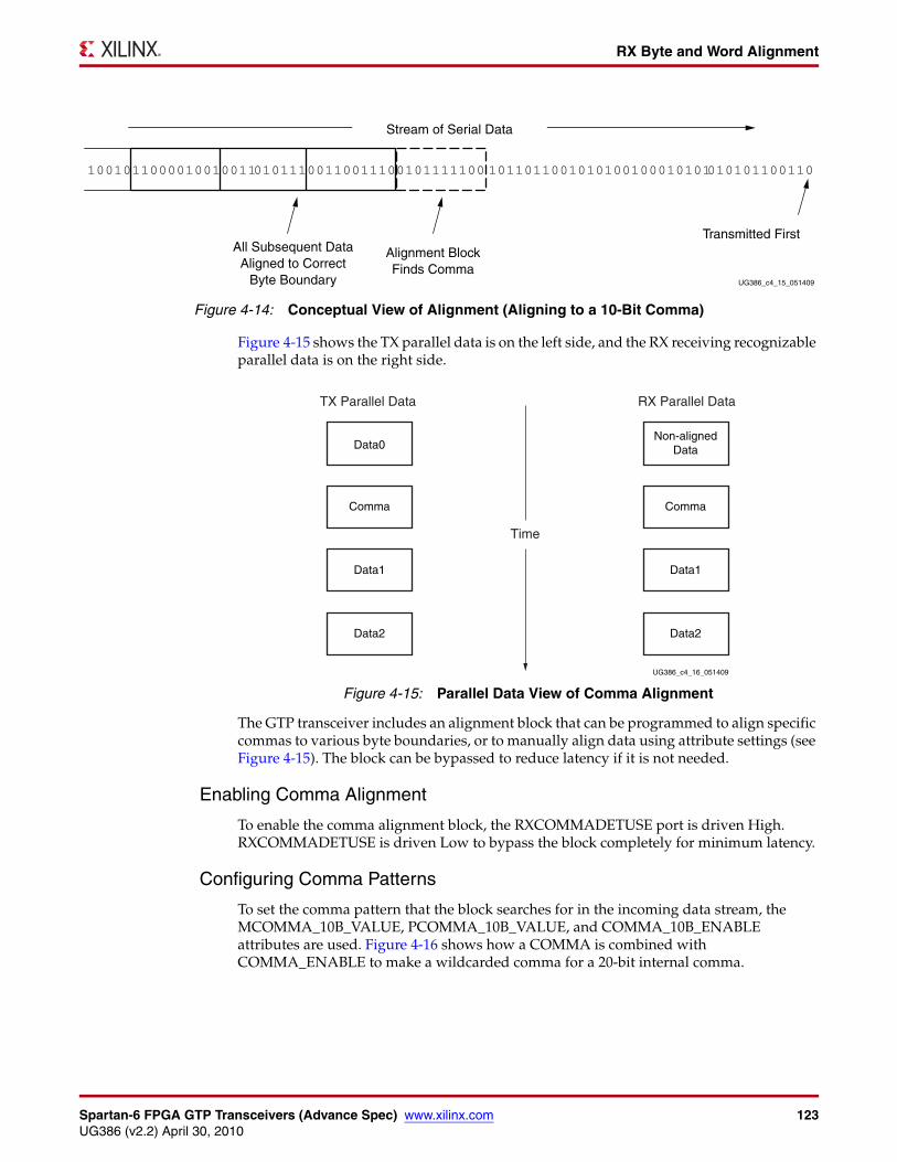
Spartan-6 FPGA GTP Transceivers (Advance Spec) www.xilinx.com 123UG386 (v2.2) April 30, 2010
RX Byte and Word Alignment
Figure 4-15 shows the TX parallel data is on the left side, and the RX receiving recognizable parallel data is on the right side.
The GTP transceiver includes an alignment block that can be programmed to align specific commas to various byte boundaries, or to manually align data using attribute settings (see Figure 4-15). The block can be bypassed to reduce latency if it is not needed.
Enabling Comma Alignment
To enable the comma alignment block, the RXCOMMADETUSE port is driven High. RXCOMMADETUSE is driven Low to bypass the block completely for minimum latency.
Configuring Comma Patterns
To set the comma pattern that the block searches for in the incoming data stream, the MCOMMA_10B_VALUE, PCOMMA_10B_VALUE, and COMMA_10B_ENABLE attributes are used. Figure 4-16 shows how a COMMA is combined with COMMA_ENABLE to make a wildcarded comma for a 20-bit internal comma.
X-Ref Target - Figure 4-14
Figure 4-14: Conceptual View of Alignment (Aligning to a 10-Bit Comma)
100101100001001001101011100110011100101111100 1011011001010100100010101010101100110
All Subsequent DataAligned to Correct
Byte Boundary
Alignment BlockFinds Comma
Transmitted First
UG386_c4_15_051409
Stream of Serial Data
X-Ref Target - Figure 4-15
Figure 4-15: Parallel Data View of Comma Alignment
TX Parallel Data RX Parallel Data
Data0
Comma
Data1
Data2
Non-alignedData
Comma
Data1
Data2
Time
UG386_c4_16_051409
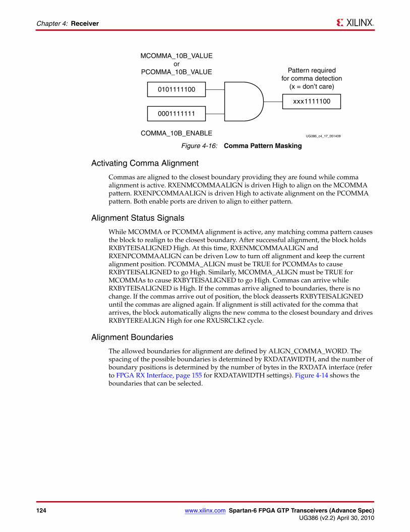
124 www.xilinx.com Spartan-6 FPGA GTP Transceivers (Advance Spec)UG386 (v2.2) April 30, 2010
Chapter 4: Receiver
Activating Comma Alignment
Commas are aligned to the closest boundary providing they are found while comma alignment is active. RXENMCOMMAALIGN is driven High to align on the MCOMMA pattern. RXENPCOMMAALIGN is driven High to activate alignment on the PCOMMA pattern. Both enable ports are driven to align to either pattern.
Alignment Status Signals
While MCOMMA or PCOMMA alignment is active, any matching comma pattern causes the block to realign to the closest boundary. After successful alignment, the block holds RXBYTEISALIGNED High. At this time, RXENMCOMMAALIGN and RXENPCOMMAALIGN can be driven Low to turn off alignment and keep the current alignment position. PCOMMA_ALIGN must be TRUE for PCOMMAs to cause RXBYTEISALIGNED to go High. Similarly, MCOMMA_ALIGN must be TRUE for MCOMMAs to cause RXBYTEISALIGNED to go High. Commas can arrive while RXBYTEISALIGNED is High. If the commas arrive aligned to boundaries, there is no change. If the commas arrive out of position, the block deasserts RXBYTEISALIGNED until the commas are aligned again. If alignment is still activated for the comma that arrives, the block automatically aligns the new comma to the closest boundary and drives RXBYTEREALIGN High for one RXUSRCLK2 cycle.
Alignment Boundaries
The allowed boundaries for alignment are defined by ALIGN_COMMA_WORD. The spacing of the possible boundaries is determined by RXDATAWIDTH, and the number of boundary positions is determined by the number of bytes in the RXDATA interface (refer to FPGA RX Interface, page 155 for RXDATAWIDTH settings). Figure 4-14 shows the boundaries that can be selected.
X-Ref Target - Figure 4-16
Figure 4-16: Comma Pattern Masking
0101111100
xxx1111100
0001111111
MCOMMA_10B_VALUEor
PCOMMA_10B_VALUE Pattern requiredfor comma detection
(x = don’t care)
COMMA_10B_ENABLE UG386_c4_17_051409
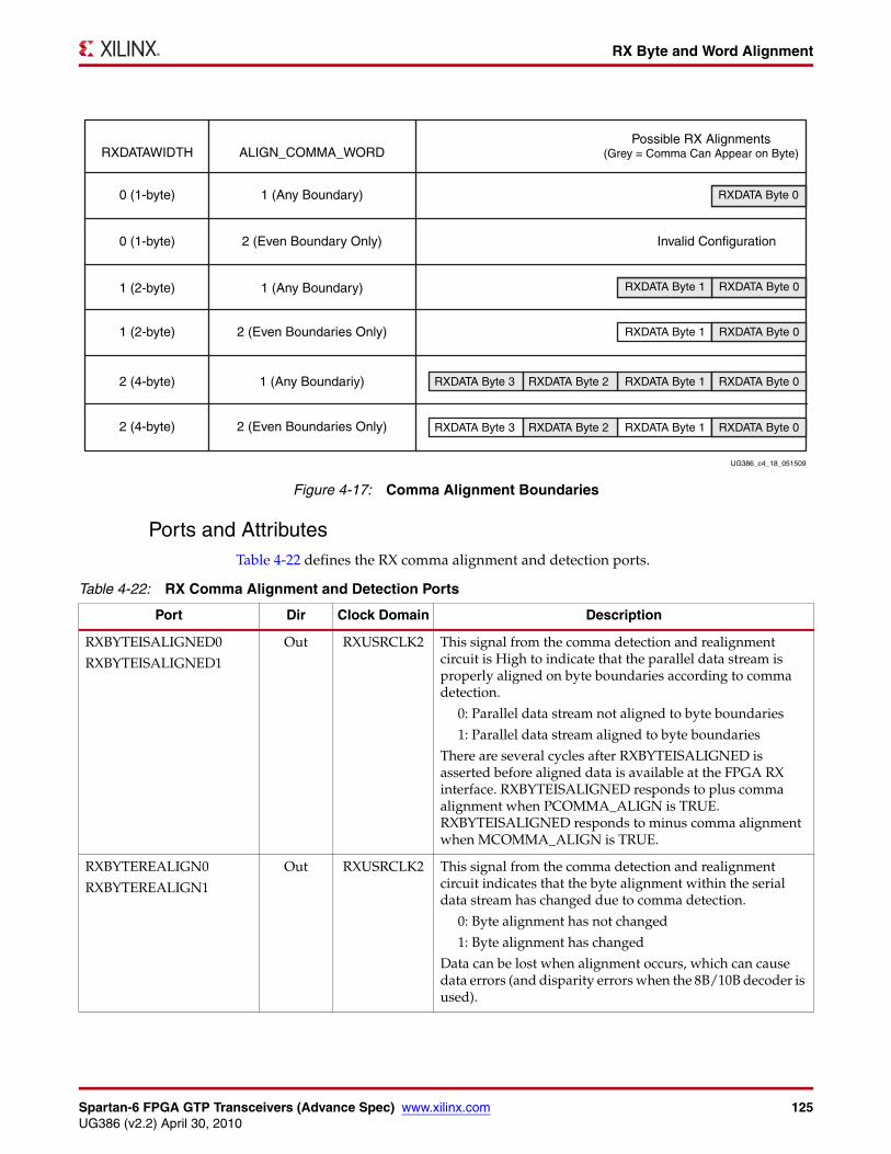
Spartan-6 FPGA GTP Transceivers (Advance Spec) www.xilinx.com 125UG386 (v2.2) April 30, 2010
RX Byte and Word Alignment
Ports and AttributesTable 4-22 defines the RX comma alignment and detection ports.
X-Ref Target - Figure 4-17
Figure 4-17: Comma Alignment Boundaries
RXDATAWIDTH
0 (1-byte)
0 (1-byte)
1 (2-byte)
1 (2-byte)
ALIGN_COMMA_WORD
1 (Any Boundary)
2 (Even Boundary Only)
1 (Any Boundary)
UG386_c4_18_051509
2 (Even Boundaries Only)
Possible RX Alignments(Grey = Comma Can Appear on Byte)
RXDATA Byte 0
Invalid Configuration
RXDATA Byte 1 RXDATA Byte 0
RXDATA Byte 1 RXDATA Byte 0
2 (4-byte) 1 (Any Boundariy) RXDATA Byte 1
RXDATA Byte 0
RXDATA Byte 0RXDATA Byte 0RXDATA Byte 3 RXDATA Byte 2
RXDATA Byte 1 RXDATA Byte 0RXDATA Byte 0RXDATA Byte 3 RXDATA Byte 22 (4-byte) 2 (Even Boundaries Only)
Table 4-22: RX Comma Alignment and Detection Ports
Port Dir Clock Domain Description
RXBYTEISALIGNED0
RXBYTEISALIGNED1
Out RXUSRCLK2 This signal from the comma detection and realignment circuit is High to indicate that the parallel data stream is properly aligned on byte boundaries according to comma detection.
0: Parallel data stream not aligned to byte boundaries
1: Parallel data stream aligned to byte boundaries
There are several cycles after RXBYTEISALIGNED is asserted before aligned data is available at the FPGA RX interface. RXBYTEISALIGNED responds to plus comma alignment when PCOMMA_ALIGN is TRUE. RXBYTEISALIGNED responds to minus comma alignment when MCOMMA_ALIGN is TRUE.
RXBYTEREALIGN0
RXBYTEREALIGN1
Out RXUSRCLK2 This signal from the comma detection and realignment circuit indicates that the byte alignment within the serial data stream has changed due to comma detection.
0: Byte alignment has not changed
1: Byte alignment has changed
Data can be lost when alignment occurs, which can cause data errors (and disparity errors when the 8B/10B decoder is used).
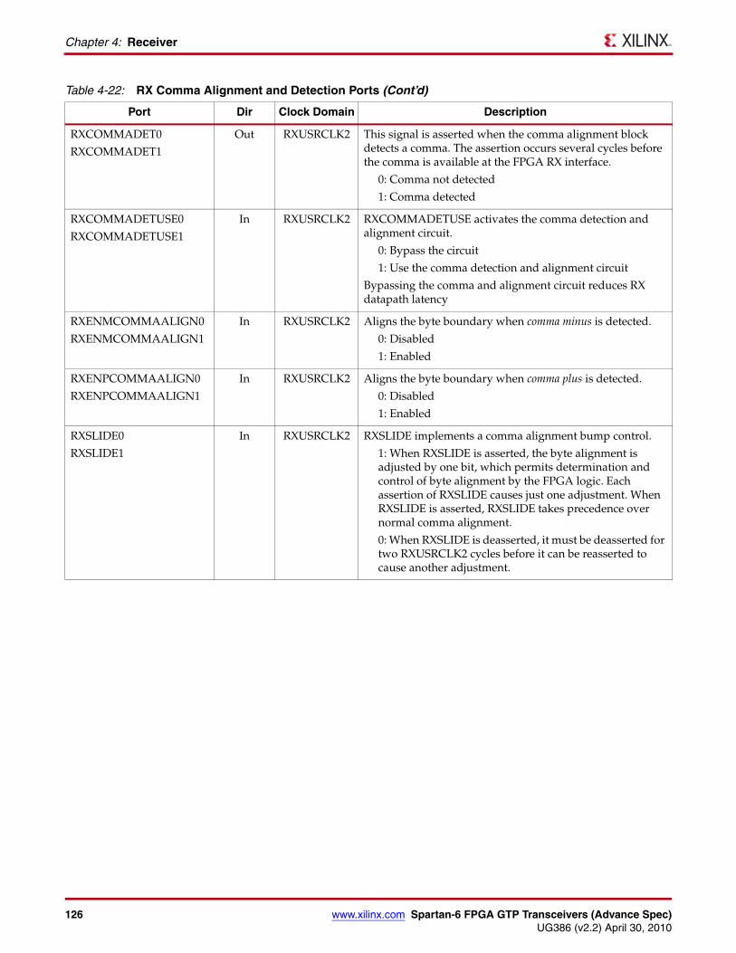
126 www.xilinx.com Spartan-6 FPGA GTP Transceivers (Advance Spec)UG386 (v2.2) April 30, 2010
Chapter 4: Receiver
RXCOMMADET0
RXCOMMADET1
Out RXUSRCLK2 This signal is asserted when the comma alignment block detects a comma. The assertion occurs several cycles before the comma is available at the FPGA RX interface.
0: Comma not detected
1: Comma detected
RXCOMMADETUSE0
RXCOMMADETUSE1
In RXUSRCLK2 RXCOMMADETUSE activates the comma detection and alignment circuit.
0: Bypass the circuit
1: Use the comma detection and alignment circuit
Bypassing the comma and alignment circuit reduces RX datapath latency
RXENMCOMMAALIGN0
RXENMCOMMAALIGN1
In RXUSRCLK2 Aligns the byte boundary when comma minus is detected.
0: Disabled
1: Enabled
RXENPCOMMAALIGN0
RXENPCOMMAALIGN1
In RXUSRCLK2 Aligns the byte boundary when comma plus is detected.
0: Disabled
1: Enabled
RXSLIDE0
RXSLIDE1
In RXUSRCLK2 RXSLIDE implements a comma alignment bump control.
1: When RXSLIDE is asserted, the byte alignment is adjusted by one bit, which permits determination and control of byte alignment by the FPGA logic. Each assertion of RXSLIDE causes just one adjustment. When RXSLIDE is asserted, RXSLIDE takes precedence over normal comma alignment.
0: When RXSLIDE is deasserted, it must be deasserted for two RXUSRCLK2 cycles before it can be reasserted to cause another adjustment.
Table 4-22: RX Comma Alignment and Detection Ports (Cont’d)
Port Dir Clock Domain Description
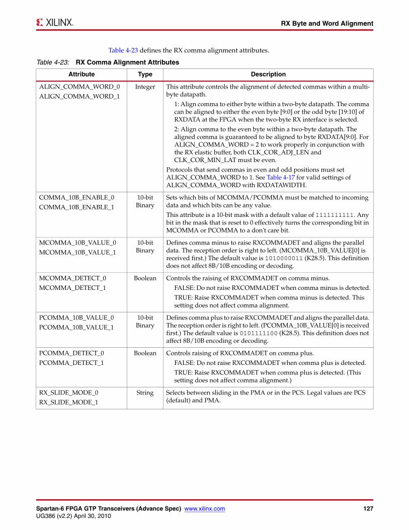
Spartan-6 FPGA GTP Transceivers (Advance Spec) www.xilinx.com 127UG386 (v2.2) April 30, 2010
RX Byte and Word Alignment
Table 4-23 defines the RX comma alignment attributes.
Table 4-23: RX Comma Alignment Attributes
Attribute Type Description
ALIGN_COMMA_WORD_0
ALIGN_COMMA_WORD_1
Integer This attribute controls the alignment of detected commas within a multi-byte datapath.
1: Align comma to either byte within a two-byte datapath. The comma can be aligned to either the even byte [9:0] or the odd byte [19:10] of RXDATA at the FPGA when the two-byte RX interface is selected.
2: Align comma to the even byte within a two-byte datapath. The aligned comma is guaranteed to be aligned to byte RXDATA[9:0]. For ALIGN_COMMA_WORD = 2 to work properly in conjunction with the RX elastic buffer, both CLK_COR_ADJ_LEN and CLK_COR_MIN_LAT must be even.
Protocols that send commas in even and odd positions must set ALIGN_COMMA_WORD to 1. See Table 4-17 for valid settings of ALIGN_COMMA_WORD with RXDATAWIDTH.
COMMA_10B_ENABLE_0
COMMA_10B_ENABLE_1
10-bit Binary
Sets which bits of MCOMMA/PCOMMA must be matched to incoming data and which bits can be any value.
This attribute is a 10-bit mask with a default value of 1111111111. Any bit in the mask that is reset to 0 effectively turns the corresponding bit in MCOMMA or PCOMMA to a don't care bit.
MCOMMA_10B_VALUE_0
MCOMMA_10B_VALUE_1
10-bit Binary
Defines comma minus to raise RXCOMMADET and aligns the parallel data. The reception order is right to left. (MCOMMA_10B_VALUE[0] is received first.) The default value is 1010000011 (K28.5). This definition does not affect 8B/10B encoding or decoding.
MCOMMA_DETECT_0
MCOMMA_DETECT_1
Boolean Controls the raising of RXCOMMADET on comma minus.
FALSE: Do not raise RXCOMMADET when comma minus is detected.
TRUE: Raise RXCOMMADET when comma minus is detected. This setting does not affect comma alignment.
PCOMMA_10B_VALUE_0
PCOMMA_10B_VALUE_1
10-bit Binary
Defines comma plus to raise RXCOMMADET and aligns the parallel data. The reception order is right to left. (PCOMMA_10B_VALUE[0] is received first.) The default value is 0101111100 (K28.5). This definition does not affect 8B/10B encoding or decoding.
PCOMMA_DETECT_0
PCOMMA_DETECT_1
Boolean Controls raising of RXCOMMADET on comma plus.
FALSE: Do not raise RXCOMMADET when comma plus is detected.
TRUE: Raise RXCOMMADET when comma plus is detected. (This setting does not affect comma alignment.)
RX_SLIDE_MODE_0
RX_SLIDE_MODE_1
String Selects between sliding in the PMA or in the PCS. Legal values are PCS (default) and PMA.
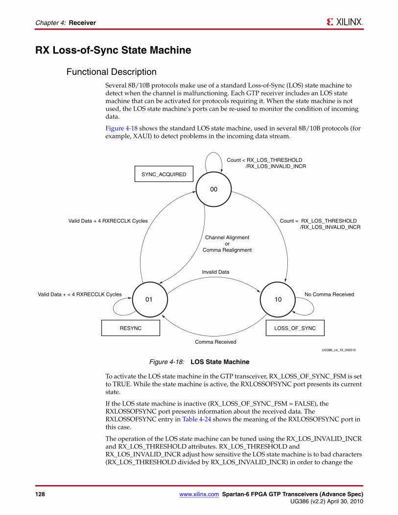
128 www.xilinx.com Spartan-6 FPGA GTP Transceivers (Advance Spec)UG386 (v2.2) April 30, 2010
Chapter 4: Receiver
RX Loss-of-Sync State Machine
Functional DescriptionSeveral 8B/10B protocols make use of a standard Loss-of-Sync (LOS) state machine to detect when the channel is malfunctioning. Each GTP receiver includes an LOS state machine that can be activated for protocols requiring it. When the state machine is not used, the LOS state machine's ports can be re-used to monitor the condition of incoming data.
Figure 4-18 shows the standard LOS state machine, used in several 8B/10B protocols (for example, XAUI) to detect problems in the incoming data stream.
To activate the LOS state machine in the GTP transceiver, RX_LOSS_OF_SYNC_FSM is set to TRUE. While the state machine is active, the RXLOSSOFSYNC port presents its current state.
If the LOS state machine is inactive (RX_LOSS_OF_SYNC_FSM = FALSE), the RXLOSSOFSYNC port presents information about the received data. The RXLOSSOFSYNC entry in Table 4-24 shows the meaning of the RXLOSSOFSYNC port in this case.
The operation of the LOS state machine can be tuned using the RX_LOS_INVALID_INCR and RX_LOS_THRESHOLD attributes. RX_LOS_THRESHOLD and RX_LOS_INVALID_INCR adjust how sensitive the LOS state machine is to bad characters (RX_LOS_THRESHOLD divided by RX_LOS_INVALID_INCR) in order to change the
X-Ref Target - Figure 4-18
Figure 4-18: LOS State Machine
00
01 10No Comma Received
Count = RX_LOS_THRESHOLD /RX_LOS_INVALID_INCR
Count < RX_LOS_THRESHOLD /RX_LOS_INVALID_INCR
Channel Alignmentor
Comma Realignment
Invalid Data
Comma ReceivedUG386_c4_19_030510
Valid Data + 4 RXRECCLK Cycles
Valid Data + < 4 RXRECCLK Cycles
SYNC_ACQUIRED
RESYNC LOSS_OF_SYNC
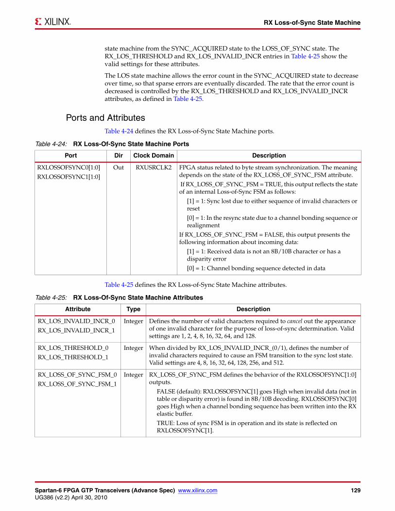
Spartan-6 FPGA GTP Transceivers (Advance Spec) www.xilinx.com 129UG386 (v2.2) April 30, 2010
RX Loss-of-Sync State Machine
state machine from the SYNC_ACQUIRED state to the LOSS_OF_SYNC state. The RX_LOS_THRESHOLD and RX_LOS_INVALID_INCR entries in Table 4-25 show the valid settings for these attributes.
The LOS state machine allows the error count in the SYNC_ACQUIRED state to decrease over time, so that sparse errors are eventually discarded. The rate that the error count is decreased is controlled by the RX_LOS_THRESHOLD and RX_LOS_INVALID_INCR attributes, as defined in Table 4-25.
Ports and AttributesTable 4-24 defines the RX Loss-of-Sync State Machine ports.
Table 4-25 defines the RX Loss-of-Sync State Machine attributes.
Table 4-24: RX Loss-Of-Sync State Machine Ports
Port Dir Clock Domain Description
RXLOSSOFSYNC0[1:0]
RXLOSSOFSYNC1[1:0]
Out RXUSRCLK2 FPGA status related to byte stream synchronization. The meaning depends on the state of the RX_LOSS_OF_SYNC_FSM attribute.
If RX_LOSS_OF_SYNC_FSM = TRUE, this output reflects the state of an internal Loss-of-Sync FSM as follows:
[1] = 1: Sync lost due to either sequence of invalid characters or reset
[0] = 1: In the resync state due to a channel bonding sequence or realignment
If RX_LOSS_OF_SYNC_FSM = FALSE, this output presents the following information about incoming data:
[1] = 1: Received data is not an 8B/10B character or has a disparity error
[0] = 1: Channel bonding sequence detected in data
Table 4-25: RX Loss-Of-Sync State Machine Attributes
Attribute Type Description
RX_LOS_INVALID_INCR_0
RX_LOS_INVALID_INCR_1
Integer Defines the number of valid characters required to cancel out the appearance of one invalid character for the purpose of loss-of-sync determination. Valid settings are 1, 2, 4, 8, 16, 32, 64, and 128.
RX_LOS_THRESHOLD_0
RX_LOS_THRESHOLD_1
Integer When divided by RX_LOS_INVALID_INCR_(0/1), defines the number of invalid characters required to cause an FSM transition to the sync lost state. Valid settings are 4, 8, 16, 32, 64, 128, 256, and 512.
RX_LOSS_OF_SYNC_FSM_0
RX_LOSS_OF_SYNC_FSM_1
Integer RX_LOSS_OF_SYNC_FSM defines the behavior of the RXLOSSOFSYNC[1:0] outputs.
FALSE (default): RXLOSSOFSYNC[1] goes High when invalid data (not in table or disparity error) is found in 8B/10B decoding. RXLOSSOFSYNC[0] goes High when a channel bonding sequence has been written into the RX elastic buffer.
TRUE: Loss of sync FSM is in operation and its state is reflected on RXLOSSOFSYNC[1].
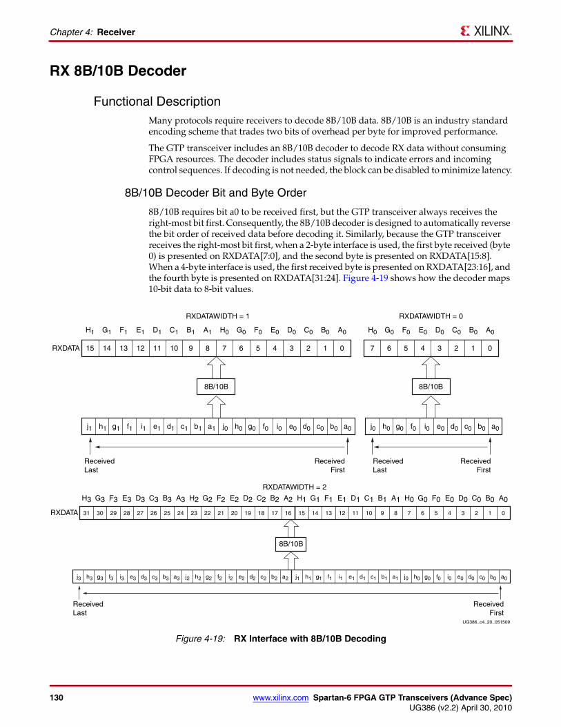
130 www.xilinx.com Spartan-6 FPGA GTP Transceivers (Advance Spec)UG386 (v2.2) April 30, 2010
Chapter 4: Receiver
RX 8B/10B Decoder
Functional DescriptionMany protocols require receivers to decode 8B/10B data. 8B/10B is an industry standard encoding scheme that trades two bits of overhead per byte for improved performance.
The GTP transceiver includes an 8B/10B decoder to decode RX data without consuming FPGA resources. The decoder includes status signals to indicate errors and incoming control sequences. If decoding is not needed, the block can be disabled to minimize latency.
8B/10B Decoder Bit and Byte Order
8B/10B requires bit a0 to be received first, but the GTP transceiver always receives the right-most bit first. Consequently, the 8B/10B decoder is designed to automatically reverse the bit order of received data before decoding it. Similarly, because the GTP transceiver receives the right-most bit first, when a 2-byte interface is used, the first byte received (byte 0) is presented on RXDATA[7:0], and the second byte is presented on RXDATA[15:8]. When a 4-byte interface is used, the first received byte is presented on RXDATA[23:16], and the fourth byte is presented on RXDATA[31:24]. Figure 4-19 shows how the decoder maps 10-bit data to 8-bit values.
X-Ref Target - Figure 4-19
Figure 4-19: RX Interface with 8B/10B Decoding
15 14 13 12 11 10 9 8 7 6 5 4 3 2 1 0
H1 G1 F1 E1 D1 C1 B1 A1 H0 G0 F0 E0 D0 C0 B0 A0 H0 G0 F0 E0 D0 C0 B0 A0
7 6 5 4 3 2 1 0
RXDATAWIDTH = 1
RXDATA
RXDATAWIDTH = 0
UG386_c4_20_051509
ReceivedLast
ReceivedLast
ReceivedFirst
ReceivedFirst
8B/10B
g0h0j0 f0 i0 e0 d0 c0 b0 a0g0h0j0 f0 i0 e0 d0 c0 b0 a0g1h1j1 f1 i1 e1 d1 c1 b1 a1
15 14 13 12 11 10 9 8 7 6 5 4 3 2 1 0
H1 G1 F1 E1 D1 C1 B1 A1 H0 G0 F0 E0 D0 C0 B0 A0
RXDATAWIDTH = 2
ReceivedLast
ReceivedFirst
8B/10B
g0h0j0 f0 i0 e0 d0 c0 b0 a0g1h1j1 f1 i1 e1 d1 c1 b1 a1
31 30 29 28 27 26 25 24 23 22 21 20 19 18 17 16
H3 G3 F3 E3 D3 C3 B3 A3 H2 G2 F2 E2 D2 C2 B2 A2
RXDATA
g2h2j2 f2 i2 e2 d2 c2 b2 a2g3h3j3 f3 i3 e3 d3 c3 b3 a3
8B/10B
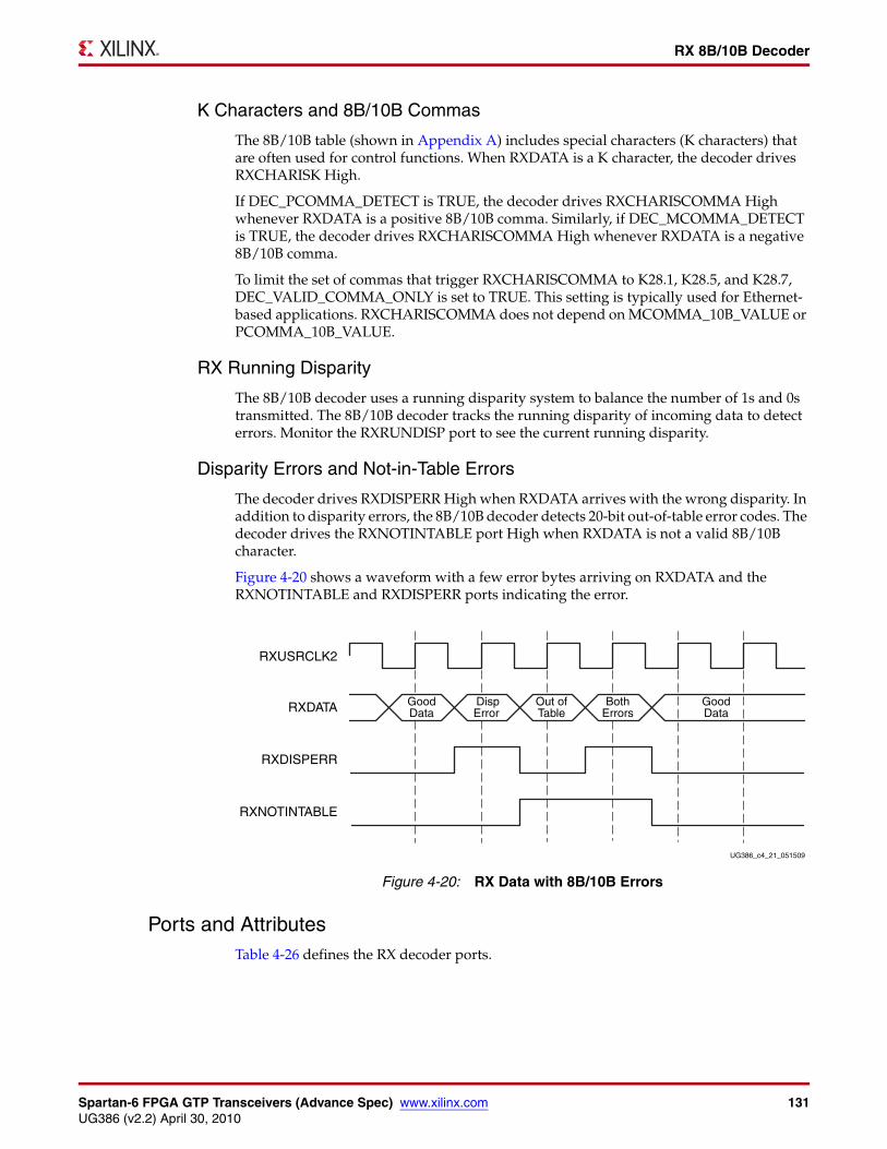
Spartan-6 FPGA GTP Transceivers (Advance Spec) www.xilinx.com 131UG386 (v2.2) April 30, 2010
RX 8B/10B Decoder
K Characters and 8B/10B Commas
The 8B/10B table (shown in Appendix A) includes special characters (K characters) that are often used for control functions. When RXDATA is a K character, the decoder drives RXCHARISK High.
If DEC_PCOMMA_DETECT is TRUE, the decoder drives RXCHARISCOMMA High whenever RXDATA is a positive 8B/10B comma. Similarly, if DEC_MCOMMA_DETECT is TRUE, the decoder drives RXCHARISCOMMA High whenever RXDATA is a negative 8B/10B comma.
To limit the set of commas that trigger RXCHARISCOMMA to K28.1, K28.5, and K28.7, DEC_VALID_COMMA_ONLY is set to TRUE. This setting is typically used for Ethernet-based applications. RXCHARISCOMMA does not depend on MCOMMA_10B_VALUE or PCOMMA_10B_VALUE.
RX Running Disparity
The 8B/10B decoder uses a running disparity system to balance the number of 1s and 0s transmitted. The 8B/10B decoder tracks the running disparity of incoming data to detect errors. Monitor the RXRUNDISP port to see the current running disparity.
Disparity Errors and Not-in-Table Errors
The decoder drives RXDISPERR High when RXDATA arrives with the wrong disparity. In addition to disparity errors, the 8B/10B decoder detects 20-bit out-of-table error codes. The decoder drives the RXNOTINTABLE port High when RXDATA is not a valid 8B/10B character.
Figure 4-20 shows a waveform with a few error bytes arriving on RXDATA and the RXNOTINTABLE and RXDISPERR ports indicating the error.
Ports and AttributesTable 4-26 defines the RX decoder ports.
X-Ref Target - Figure 4-20
Figure 4-20: RX Data with 8B/10B Errors
RXUSRCLK2
RXDATA
RXDISPERR
RXNOTINTABLE
GoodData
GoodData
BothErrors
Out ofTable
DispError
UG386_c4_21_051509
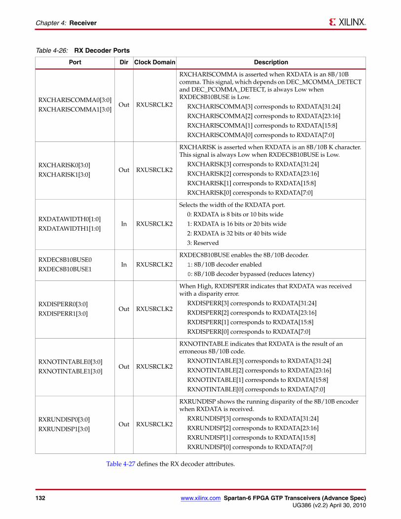
132 www.xilinx.com Spartan-6 FPGA GTP Transceivers (Advance Spec)UG386 (v2.2) April 30, 2010
Chapter 4: Receiver
Table 4-27 defines the RX decoder attributes.
Table 4-26: RX Decoder Ports
Port Dir Clock Domain Description
RXCHARISCOMMA0[3:0]
RXCHARISCOMMA1[3:0]Out RXUSRCLK2
RXCHARISCOMMA is asserted when RXDATA is an 8B/10B comma. This signal, which depends on DEC_MCOMMA_DETECT and DEC_PCOMMA_DETECT, is always Low when RXDEC8B10BUSE is Low.
RXCHARISCOMMA[3] corresponds to RXDATA[31:24]
RXCHARISCOMMA[2] corresponds to RXDATA[23:16]
RXCHARISCOMMA[1] corresponds to RXDATA[15:8]
RXCHARISCOMMA[0] corresponds to RXDATA[7:0]
RXCHARISK0[3:0]
RXCHARISK1[3:0]Out RXUSRCLK2
RXCHARISK is asserted when RXDATA is an 8B/10B K character. This signal is always Low when RXDEC8B10BUSE is Low.
RXCHARISK[3] corresponds to RXDATA[31:24]
RXCHARISK[2] corresponds to RXDATA[23:16]
RXCHARISK[1] corresponds to RXDATA[15:8]
RXCHARISK[0] corresponds to RXDATA[7:0]
RXDATAWIDTH0[1:0]
RXDATAWIDTH1[1:0]In RXUSRCLK2
Selects the width of the RXDATA port.
0: RXDATA is 8 bits or 10 bits wide
1: RXDATA is 16 bits or 20 bits wide
2: RXDATA is 32 bits or 40 bits wide
3: Reserved
RXDEC8B10BUSE0
RXDEC8B10BUSE1In RXUSRCLK2
RXDEC8B10BUSE enables the 8B/10B decoder.
1: 8B/10B decoder enabled
0: 8B/10B decoder bypassed (reduces latency)
RXDISPERR0[3:0]
RXDISPERR1[3:0]Out RXUSRCLK2
When High, RXDISPERR indicates that RXDATA was received with a disparity error.
RXDISPERR[3] corresponds to RXDATA[31:24]
RXDISPERR[2] corresponds to RXDATA[23:16]
RXDISPERR[1] corresponds to RXDATA[15:8]
RXDISPERR[0] corresponds to RXDATA[7:0]
RXNOTINTABLE0[3:0]
RXNOTINTABLE1[3:0]Out RXUSRCLK2
RXNOTINTABLE indicates that RXDATA is the result of an erroneous 8B/10B code.
RXNOTINTABLE[3] corresponds to RXDATA[31:24]
RXNOTINTABLE[2] corresponds to RXDATA[23:16]
RXNOTINTABLE[1] corresponds to RXDATA[15:8]
RXNOTINTABLE[0] corresponds to RXDATA[7:0]
RXRUNDISP0[3:0]
RXRUNDISP1[3:0]Out RXUSRCLK2
RXRUNDISP shows the running disparity of the 8B/10B encoder when RXDATA is received.
RXRUNDISP[3] corresponds to RXDATA[31:24]
RXRUNDISP[2] corresponds to RXDATA[23:16]
RXRUNDISP[1] corresponds to RXDATA[15:8]
RXRUNDISP[0] corresponds to RXDATA[7:0]
Spartan-6 FPGA GTP Transceivers (Advance Spec) www.xilinx.com 133UG386 (v2.2) April 30, 2010
RX Elastic Buffer Bypass
RX Elastic Buffer Bypass
Functional DescriptionAn advanced feature of Spartan-6 FPGA GTP transceivers that is not recommended for normal operation is bypassing of the RX elastic buffer. When the RX elastic buffer is bypassed, a process called RX phase alignment must be performed to match or adjust the phase difference between the PMA parallel clock domain (XCLK) and the PCS parallel clock domain (RXUSRCLK). In addition to the RX phase alignment process, utilizing the GTPCLKFBWEST and GTPCLKFBEAST dedicated feedback paths from the GTP transceiver to a DCM or PLL adjusts RXUSRCLK to compensate for temperature and voltage variations. Figure 4-26, page 141 shows the XCLK and RXUSRCLK domains. Table 4-30, page 141 shows the trade-offs between the buffer and the buffer bypass modes.
The RX elastic buffer can be bypassed to reduce latency when RXRECCLK is used to source RXUSRCLK and RXUSRCLK2. When the RX elastic buffer is bypassed, latency through the RX datapath is low and deterministic, but clock correction and channel bonding are not available.
Figure 4-21 shows how phase alignment allows the RX elastic buffer to be bypassed. Before phase alignment, there is no guaranteed phase relationship between the parallel clock generated from the recovered clock in the CDR circuit (XCLK) and the PCS parallel clocks from the FPGA logic (RXUSRCLK). Phase alignment causes RXRECCLK from the CDR to be adjusted so that there is no significant phase difference between XCLK and RXUSRCLK.
Table 4-27: RX Decoder Attributes
Attributes Type Description
DEC_MCOMMA_DETECT_0
DEC_MCOMMA_DETECT_1Boolean
Enables detection of negative 8B/10B commas:
TRUE: RXCHARISCOMMA is asserted when RXDATA is a negative 8B/10B comma
FALSE: RXCHARISCOMMA does not respond to negative 8B/10B commas
DEC_PCOMMA_DETECT_0
DEC_PCOMMA_DETECT_1Boolean
Enables detection of positive 8B/10B commas:
TRUE: RXCHARISCOMMA is asserted when RXDATA is a positive 8B/10B comma
FALSE: RXCHARISCOMMA does not respond to positive 8B/10B commas
DEC_VALID_COMMA_ONLY_0
DEC_VALID_COMMA_ONLY_1Boolean
Limits the set of commas to which RXCHARISCOMMA responds.
TRUE: RXCHARISCOMMA is asserted only for K28.1, K28.5, and K28.7 (see 8B/10B K character table in Appendix A, 8B/10B Valid Characters).
FALSE: RXCHARISCOMMA responds to any positive or negative 8B/10B comma, depending on the settings for DEC_MCOMMA_DETECT and DEC_PCOMMA_DETECT
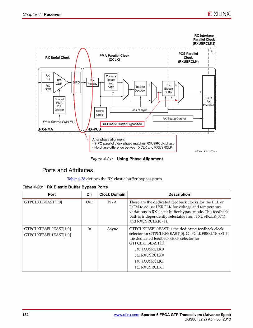
134 www.xilinx.com Spartan-6 FPGA GTP Transceivers (Advance Spec)UG386 (v2.2) April 30, 2010
Chapter 4: Receiver
Ports and AttributesTable 4-28 defines the RX elastic buffer bypass ports.
X-Ref Target - Figure 4-21
Figure 4-21: Using Phase Alignment
UG386_c4_22_100109
After phase alignment:- SIPO parallel clock phase matches RXUSRCLK phase- No phase difference between XCLK and RXUSRCLK
RX Elastic Buffer Bypassed
PMA Parallel Clock(XCLK)
RX Serial ClockPCS Parallel
Clock(RXUSRCLK)
RX InterfaceParallel Clock(RXUSRCLK2)
RX-PMA RX-PCS
From Shared PMA PLL
RXEQ
RXOOB
SIPO
10B/8BDecoder
FPGARX
Interface
RXPolarity
Loss of Sync
RX Status Control
PRBSCheck
RXCDR
SharedPMAPLL
Divider
CommaDetect
andAlign RX
ElasticBuffer
Table 4-28: RX Elastic Buffer Bypass Ports
Port Dir Clock Domain Description
GTPCLKFBEAST[1:0] Out N/A These are the dedicated feedback clocks for the PLL or DCM to adjust USRCLK for voltage and temperature variations in RX elastic buffer bypass mode. This feedback path is independently selectable from TXUSRCLK(0/1) and RXUSRCLK(0/1).
GTPCLKFBSEL0EAST[1:0]
GTPCLKFBSEL1EAST[1:0]
In Async GTPCLKFBSEL0EAST is the dedicated feedback clock selector for GTPCLKFBEAST[0]. GTPCLKFBSEL1EAST is the dedicated feedback clock selector for GTPCLKFBEAST[1].
00: TXUSRCLK0
01: RXUSRCLK0
10: TXUSRCLK1
11: RXUSRCLK1

Spartan-6 FPGA GTP Transceivers (Advance Spec) www.xilinx.com 135UG386 (v2.2) April 30, 2010
RX Elastic Buffer Bypass
GTPCLKFBSEL0WEST[1:0]
GTPCLKFBSEL1WEST[1:0]
In Async GTPCLKFBSEL0WEST is the dedicated feedback clock selector for GTPCLKFBWEST[0]. GTPCLKFBSEL1WEST is the dedicated feedback clock selector for GTPCLKFBWEST[1].
00: TXUSRCLK0
01: RXUSRCLK0
10: TXUSRCLK1
11: RXUSRCLK1
GTPCLKFBWEST[1:0] Out N/A These are the dedicated feedback clocks for the PLL or DCM to adjust USRCLK for voltage and temperature variations in RX elastic buffer bypass mode. This feedback path is independently selectable from TXUSRCLK(0/1) and RXUSRCLK(0/1).
GTPCLKOUT0[1:0]
GTPCLKOUT1[1:0]
Out N/A GTPCLKOUT is the recommended signal port to bring clocks inside the GTPA1_DUAL tile to the FPGA logic.
GTPCLKOUT[1] must be used in RX elastic buffer bypass mode.
GTPCLKOUT[0] outputs either TXOUTCLK or REFCLKPLL depending on CLK_OUT_GTP_SEL. GTPCLKOUT[1] outputs RXRECCLK (required for RX elastic buffer bypass).
PLLLKDET0
PLLLKDET1
Out Async This port indicates that the VCO rate is within acceptable tolerances of the desired rate when High. The GTP transceiver does not operate reliably until this condition is met.
PLLLKDETEN0
PLLLKDETEN1
In Async This port enables the PLL lock detector when High.
RXENPMAPHASEALIGN0
RXENPMAPHASEALIGN1
In Async When asserted High, the RX phase-alignment circuit is enabled. This allows XCLK to align with RXUSRCLK when RXPMASETPHASE is asserted.
RXPMASETPHASE0
RXPMASETPHASE1
In Async When asserted High, the GTP transceiver aligns XCLK with RXUSRCLK, allowing the RX elastic buffer to be bypassed.
RXRECCLK0
RXRECCLK1
Out N/A These ports are the recovered clocks derived from the RX Clock Data Recovery circuit. They clock the RX logic between the PMA and the RX elastic buffer. These ports are reserved for the FPGA logic only.
RXUSRCLK0
RXUSRCLK1
In N/A This port is used to provide a clock for the internal RX PCS parallel datapath. This clock must always be provided.
Table 4-28: RX Elastic Buffer Bypass Ports (Cont’d)
Port Dir Clock Domain Description
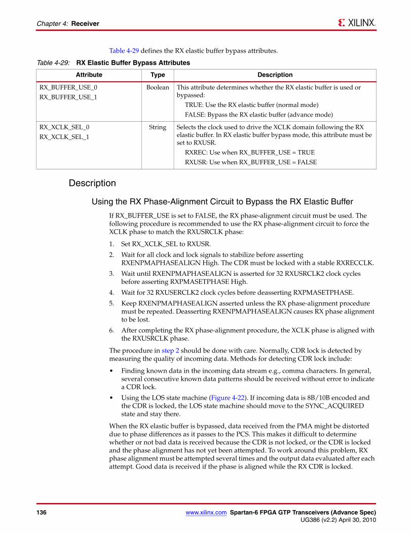
136 www.xilinx.com Spartan-6 FPGA GTP Transceivers (Advance Spec)UG386 (v2.2) April 30, 2010
Chapter 4: Receiver
Table 4-29 defines the RX elastic buffer bypass attributes.
Description
Using the RX Phase-Alignment Circuit to Bypass the RX Elastic Buffer
If RX_BUFFER_USE is set to FALSE, the RX phase-alignment circuit must be used. The following procedure is recommended to use the RX phase-alignment circuit to force the XCLK phase to match the RXUSRCLK phase:
1. Set RX_XCLK_SEL to RXUSR.
2. Wait for all clock and lock signals to stabilize before asserting RXENPMAPHASEALIGN High. The CDR must be locked with a stable RXRECCLK.
3. Wait until RXENPMAPHASEALIGN is asserted for 32 RXUSRCLK2 clock cycles before asserting RXPMASETPHASE High.
4. Wait for 32 RXUSERCLK2 clock cycles before deasserting RXPMASETPHASE.
5. Keep RXENPMAPHASEALIGN asserted unless the RX phase-alignment procedure must be repeated. Deasserting RXENPMAPHASEALIGN causes RX phase alignment to be lost.
6. After completing the RX phase-alignment procedure, the XCLK phase is aligned with the RXUSRCLK phase.
The procedure in step 2 should be done with care. Normally, CDR lock is detected by measuring the quality of incoming data. Methods for detecting CDR lock include:
• Finding known data in the incoming data stream e.g., comma characters. In general, several consecutive known data patterns should be received without error to indicate a CDR lock.
• Using the LOS state machine (Figure 4-22). If incoming data is 8B/10B encoded and the CDR is locked, the LOS state machine should move to the SYNC_ACQUIRED state and stay there.
When the RX elastic buffer is bypassed, data received from the PMA might be distorted due to phase differences as it passes to the PCS. This makes it difficult to determine whether or not bad data is received because the CDR is not locked, or the CDR is locked and the phase alignment has not yet been attempted. To work around this problem, RX phase alignment must be attempted several times and the output data evaluated after each attempt. Good data is received if the phase is aligned while the RX CDR is locked.
Table 4-29: RX Elastic Buffer Bypass Attributes
Attribute Type Description
RX_BUFFER_USE_0
RX_BUFFER_USE_1
Boolean This attribute determines whether the RX elastic buffer is used or bypassed:
TRUE: Use the RX elastic buffer (normal mode)
FALSE: Bypass the RX elastic buffer (advance mode)
RX_XCLK_SEL_0
RX_XCLK_SEL_1
String Selects the clock used to drive the XCLK domain following the RX elastic buffer. In RX elastic buffer bypass mode, this attribute must be set to RXUSR.
RXREC: Use when RX_BUFFER_USE = TRUE
RXUSR: Use when RX_BUFFER_USE = FALSE

Spartan-6 FPGA GTP Transceivers (Advance Spec) www.xilinx.com 137UG386 (v2.2) April 30, 2010
RX Elastic Buffer Bypass
The flow diagram in Figure 4-22 shows the steps required for successful RX phase alignment. Any number of clock cycles can be used for the CDR lock time, but using a larger number decreases the number of cycles through the states.X-Ref Target - Figure 4-22
Figure 4-22: Steps Required for Successful RX Phase Alignment
Wait for CDR to Lock
FinalRXPMASETPHASEAssertion for Phase
Alignment with KnownCDR Lock (32 Cycles)
AssertRXPMASETPHASE
32 RXUSRCLK2Cycles to
Phase Align
Wait for PLL Lockand DCM/PLL Lock.RXN/RXP Should Be
Driven
Fail
UG386_c4_33_100609
Pass
Phase AlignmentDone
RESET
Evaluate CDR Lock byChecking Data or Using
LOS State Machine
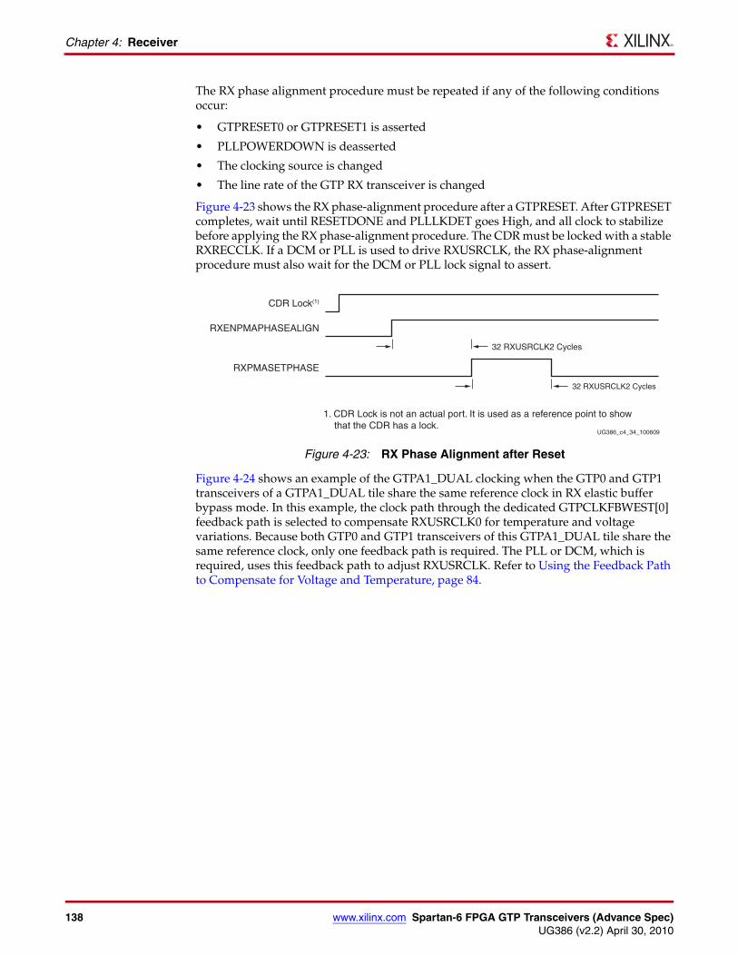
138 www.xilinx.com Spartan-6 FPGA GTP Transceivers (Advance Spec)UG386 (v2.2) April 30, 2010
Chapter 4: Receiver
The RX phase alignment procedure must be repeated if any of the following conditions occur:
• GTPRESET0 or GTPRESET1 is asserted
• PLLPOWERDOWN is deasserted
• The clocking source is changed
• The line rate of the GTP RX transceiver is changed
Figure 4-23 shows the RX phase-alignment procedure after a GTPRESET. After GTPRESET completes, wait until RESETDONE and PLLLKDET goes High, and all clock to stabilize before applying the RX phase-alignment procedure. The CDR must be locked with a stable RXRECCLK. If a DCM or PLL is used to drive RXUSRCLK, the RX phase-alignment procedure must also wait for the DCM or PLL lock signal to assert.
Figure 4-24 shows an example of the GTPA1_DUAL clocking when the GTP0 and GTP1 transceivers of a GTPA1_DUAL tile share the same reference clock in RX elastic buffer bypass mode. In this example, the clock path through the dedicated GTPCLKFBWEST[0] feedback path is selected to compensate RXUSRCLK0 for temperature and voltage variations. Because both GTP0 and GTP1 transceivers of this GTPA1_DUAL tile share the same reference clock, only one feedback path is required. The PLL or DCM, which is required, uses this feedback path to adjust RXUSRCLK. Refer to Using the Feedback Path to Compensate for Voltage and Temperature, page 84.
X-Ref Target - Figure 4-23
Figure 4-23: RX Phase Alignment after Reset
UG386_c4_34_100609
CDR Lock(1)
RXENPMAPHASEALIGN
RXPMASETPHASE
1. CDR Lock is not an actual port. It is used as a reference point to show that the CDR has a lock.
32 RXUSRCLK2 Cycles
32 RXUSRCLK2 Cycles
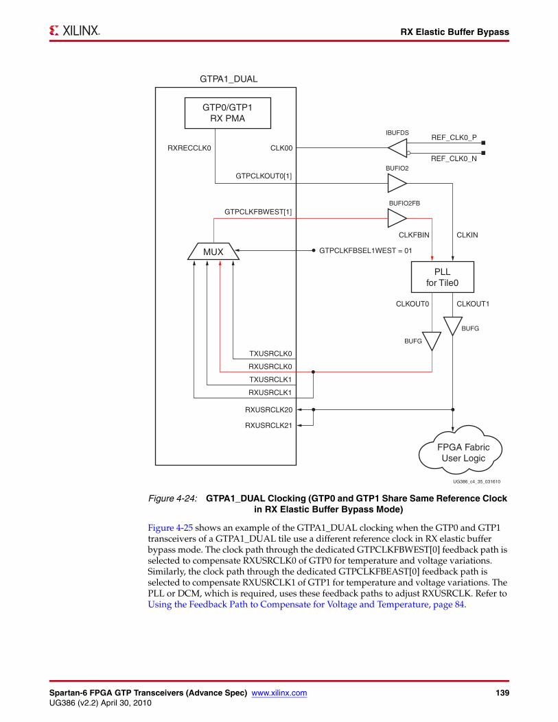
Spartan-6 FPGA GTP Transceivers (Advance Spec) www.xilinx.com 139UG386 (v2.2) April 30, 2010
RX Elastic Buffer Bypass
Figure 4-25 shows an example of the GTPA1_DUAL clocking when the GTP0 and GTP1 transceivers of a GTPA1_DUAL tile use a different reference clock in RX elastic buffer bypass mode. The clock path through the dedicated GTPCLKFBWEST[0] feedback path is selected to compensate RXUSRCLK0 of GTP0 for temperature and voltage variations. Similarly, the clock path through the dedicated GTPCLKFBEAST[0] feedback path is selected to compensate RXUSRCLK1 of GTP1 for temperature and voltage variations. The PLL or DCM, which is required, uses these feedback paths to adjust RXUSRCLK. Refer to Using the Feedback Path to Compensate for Voltage and Temperature, page 84.
X-Ref Target - Figure 4-24
Figure 4-24: GTPA1_DUAL Clocking (GTP0 and GTP1 Share Same Reference Clock in RX Elastic Buffer Bypass Mode)
UG386_c4_35_031610
IBUFDSREF_CLK0_P
REF_CLK0_N
CLKIN
CLKOUT1
CLK00
GTPCLKOUT0[1]
RXRECCLK0
GTPCLKFBWEST[1]
TXUSRCLK1
RXUSRCLK1
TXUSRCLK0
RXUSRCLK0
RXUSRCLK20
RXUSRCLK21
GTPCLKFBSEL1WEST = 01
CLKFBIN
PLLfor Tile0
GTP0/GTP1RX PMA
GTPA1_DUAL
BUFIO2
BUFG
BUFIO2FB
CLKOUT0
BUFG
MUX
FPGA FabricUser Logic
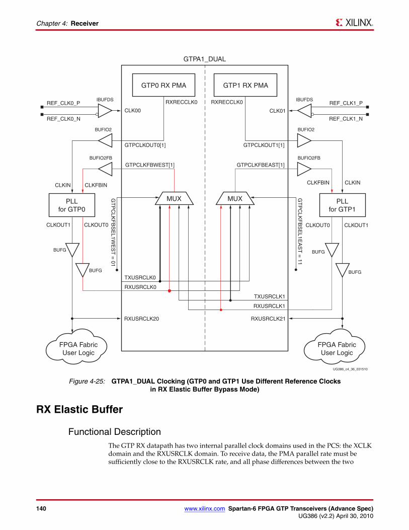
140 www.xilinx.com Spartan-6 FPGA GTP Transceivers (Advance Spec)UG386 (v2.2) April 30, 2010
Chapter 4: Receiver
RX Elastic Buffer
Functional DescriptionThe GTP RX datapath has two internal parallel clock domains used in the PCS: the XCLK domain and the RXUSRCLK domain. To receive data, the PMA parallel rate must be sufficiently close to the RXUSRCLK rate, and all phase differences between the two
X-Ref Target - Figure 4-25
Figure 4-25: GTPA1_DUAL Clocking (GTP0 and GTP1 Use Different Reference Clocks in RX Elastic Buffer Bypass Mode)
UG386_c4_36_031510
IBUFDSREF_CLK1_P
REF_CLK1_N
CLKIN
CLKOUT1
CLK01CLK00
GTPCLKOUT1[1]
RXRECCLK0
GTPCLKFBEAST[1]
TXUSRCLK1
RXUSRCLK1
RXUSRCLK21
GT
PC
LKF
BS
EL1E
AS
T =
11
CLKFBIN
PLLfor GTP1
GTP1 RX PMA
BUFIO2
BUFG
BUFG
GTPCLKOUT0[1]
RXRECCLK0
BUFIO2FB
CLKOUT0
MUX
IBUFDSREF_CLK0_P
REF_CLK0_N
CLKIN
CLKOUT1
GTPCLKFBWEST[1]
TXUSRCLK0
RXUSRCLK0
RXUSRCLK20
GT
PC
LKF
BS
EL1W
ES
T =
01
CLKFBIN
PLLfor GTP0
GTP0 RX PMA
GTPA1_DUAL
BUFIO2
BUFG
BUFIO2FB
CLKOUT0
BUFG
MUX
FPGA FabricUser Logic
FPGA FabricUser Logic
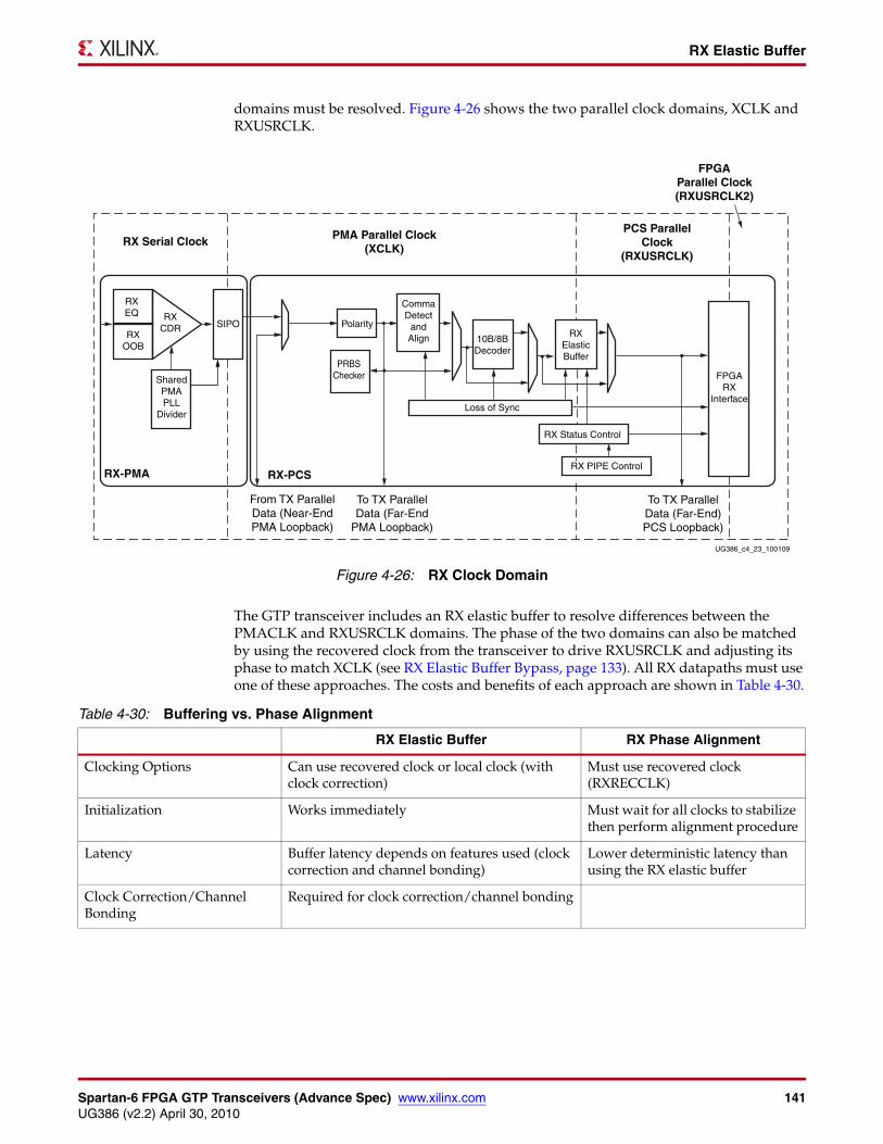
Spartan-6 FPGA GTP Transceivers (Advance Spec) www.xilinx.com 141UG386 (v2.2) April 30, 2010
RX Elastic Buffer
domains must be resolved. Figure 4-26 shows the two parallel clock domains, XCLK and RXUSRCLK.
The GTP transceiver includes an RX elastic buffer to resolve differences between the PMACLK and RXUSRCLK domains. The phase of the two domains can also be matched by using the recovered clock from the transceiver to drive RXUSRCLK and adjusting its phase to match XCLK (see RX Elastic Buffer Bypass, page 133). All RX datapaths must use one of these approaches. The costs and benefits of each approach are shown in Table 4-30.
X-Ref Target - Figure 4-26
Figure 4-26: RX Clock Domain
UG386_c4_23_100109
PMA Parallel Clock(XCLK)
RX Serial ClockPCS Parallel
Clock(RXUSRCLK)
FPGAParallel Clock(RXUSRCLK2)
RX-PMA RX-PCS
RXEQ
RXOOB
SIPO
10B/8BDecoder
FPGARX
Interface
Polarity
Loss of Sync
RX Status Control
PRBSChecker
RXCDR
SharedPMAPLL
Divider
CommaDetect
andAlign RX
ElasticBuffer
From TX ParallelData (Near-EndPMA Loopback)
To TX ParallelData (Far-End
PMA Loopback)
RX PIPE Control
To TX ParallelData (Far-End)PCS Loopback)
Table 4-30: Buffering vs. Phase Alignment
RX Elastic Buffer RX Phase Alignment
Clocking Options Can use recovered clock or local clock (with clock correction)
Must use recovered clock (RXRECCLK)
Initialization Works immediately Must wait for all clocks to stabilize then perform alignment procedure
Latency Buffer latency depends on features used (clock correction and channel bonding)
Lower deterministic latency than using the RX elastic buffer
Clock Correction/Channel Bonding
Required for clock correction/channel bonding
142 www.xilinx.com Spartan-6 FPGA GTP Transceivers (Advance Spec)UG386 (v2.2) April 30, 2010
Chapter 4: Receiver
Ports and AttributesTable 4-31 defines the RX elastic buffer ports.
Table 4-32 defines the RX elastic buffer attributes.
Using the RX Elastic Buffer for Channel Bonding or Clock CorrectionThe RX elastic buffer is also used for clock correction (see RX Clock Correction) and channel bonding (see RX Channel Bonding, page 149). Clock correction is used in cases where PMACLK and RXUSRCLK are not frequency matched. Table 4-33 lists common clock configurations and shows whether they require clock correction.
Table 4-31: RX Elastic Buffer Ports
Port Dir Clock Domain Description
RXBUFRESET0
RXBUFRESET1
In Asynchronous Resets the RX elastic buffer logic and re-initializes the RX elastic buffer.
RXBUFSTATUS0[2:0]
RXBUFSTATUS1[2:0]
Out RXUSRCLK2 Indicates the status of the RX elastic buffer as follows:
000: Nominal condition
001: Number of bytes in the buffer are less than CLK_COR_MIN_LAT
010: Number of bytes in the buffer are greater than CLK_COR_MAX_LAT
101: RX elastic buffer underflow(1)
110: RX elastic buffer overflow(1)
Notes: 1. If an RX elastic buffer overflow or an RX elastic buffer underflow condition occurs, the content of the RX elastic buffer becomes
invalid, and the RX elastic buffer needs re-initialization by asserting/deasserting RXBUFRESET.
Table 4-32: RX Elastic Buffer Attributes
Attribute Type Description
RX_BUFFER_USE_0
RX_BUFFER_USE_1
Boolean Use or bypass the RX elastic buffer.
TRUE: Use the RX elastic buffer (normal mode).
FALSE: Permanently bypass the RX elastic buffer.
RX_EN_IDLE_RESET_BUF_0
RX_EN_IDLE_RESET_BUF_1
Boolean Enable or disable the automatic RX elastic buffer reset.
TRUE: Enable the automatic RX elastic buffer reset when valid signals are not present on the RXN/RXP inputs.
FALSE: Disable the automatic RX elastic buffer reset when valid signals are not present on the RXN/RXP inputs.
RX_IDLE_HI_CNT_0
RX_IDLE_HI_CNT_1
4-bit Binary
Determines count value after which an assertion of reset due to RX_EN_IDLE_RESET_BUF will be triggered after valid data is no longer present on the RXP/RXN lines. Use the GTP Transceiver Wizard default.
RX_IDLE_LO_CNT_0
RX_IDLE_LO_CNT_1
4-bit Binary
Determines count value after which a deassertion of reset due to RX_EN_IDLE_RESET_BUF will be triggered after valid data once again present on the RXP/RXN lines. Use the GTP Transceiver Wizard default.
RX_XCLK_SEL_0
RX_XCLK_SEL_1
String Selects the clock used to drive the XCLK domain.
“RXREC”: (default) XCLK domain driven by recovered clock from CDR.
“RXUSR”: RXUSRCLK port drives RX parallel clock domain. Use this mode when bypassing the RX elastic buffer.
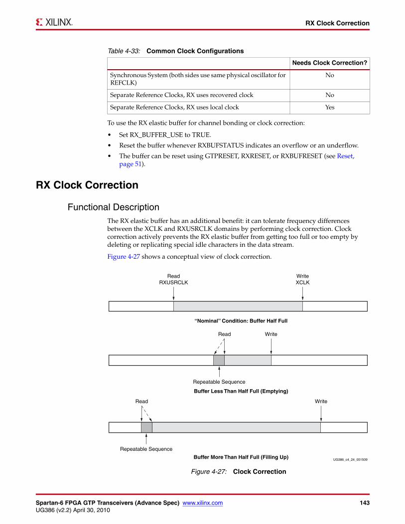
Spartan-6 FPGA GTP Transceivers (Advance Spec) www.xilinx.com 143UG386 (v2.2) April 30, 2010
RX Clock Correction
To use the RX elastic buffer for channel bonding or clock correction:
• Set RX_BUFFER_USE to TRUE.
• Reset the buffer whenever RXBUFSTATUS indicates an overflow or an underflow.
• The buffer can be reset using GTPRESET, RXRESET, or RXBUFRESET (see Reset, page 51).
RX Clock Correction
Functional DescriptionThe RX elastic buffer has an additional benefit: it can tolerate frequency differences between the XCLK and RXUSRCLK domains by performing clock correction. Clock correction actively prevents the RX elastic buffer from getting too full or too empty by deleting or replicating special idle characters in the data stream.
Figure 4-27 shows a conceptual view of clock correction.
Table 4-33: Common Clock Configurations
Needs Clock Correction?
Synchronous System (both sides use same physical oscillator for REFCLK)
No
Separate Reference Clocks, RX uses recovered clock No
Separate Reference Clocks, RX uses local clock Yes
X-Ref Target - Figure 4-27
Figure 4-27: Clock Correction
WriteXCLK
“Nominal” Condition: Buffer Half Full
Buffer Less Than Half Full (Emptying)
Buffer More Than Half Full (Filling Up)
ReadRXUSRCLK
WriteRead
Repeatable Sequence
Write
UG386_c4_24_051509
Repeatable Sequence
Read
144 www.xilinx.com Spartan-6 FPGA GTP Transceivers (Advance Spec)UG386 (v2.2) April 30, 2010
Chapter 4: Receiver
Clock correction should be used whenever there is a frequency difference between XCLK and RXUSRCLK. It can be avoided by using the same frequency source for TX and RX, or by using the recovered clock to drive RXUSRCLK. The section RX Elastic Buffer, page 140 has more details about the steps required if clock correction is not used.
Ports and AttributesTable 4-34 defines the RX clock correction ports.
Table 4-35 defines the RX clock correction attributes.
Table 4-34: RX Clock Correction Ports
Port Dir Clock Domain Description
RXBUFRESET0
RXBUFRESET1
In Async Resets the RX elastic buffer logic and re-initializes the RX elastic buffer.
RXBUFSTATUS0[2:0]
RXBUFSTATUS1[2:0]
Out RXUSRCLK2 Indicates the status of the RX elastic buffer as follows:
000: Nominal condition
001: Number of bytes in the buffer are less than CLK_COR_MIN_LAT
010: Number of bytes in the buffer are greater than CLK_COR_MAX_LAT
101: RX elastic buffer underflow(1)
110: RX elastic buffer overflow(1)
RXCLKCORCNT0[2:0]
RXCLKCORCNT1[2:0]
Out RXUSRCLK2 Reports the clock correction status of the RX elastic buffer:
000: No clock correction
001: 1 sequence skipped
010: 2 sequences skipped
011: 3 sequences skipped
100: 4 sequences skipped
101: Reserved
110: 2 sequences added
111: 1 sequence added
Notes: 1. If an RX elastic buffer overflow or an RX elastic buffer underflow condition occurs, the content of the RX elastic buffer becomes
invalid, and the RX elastic buffer needs re-initialization by asserting/deasserting RXBUFRESET.
Table 4-35: RX Clock Correction Attributes
Attribute Type Description
CLK_COR_ADJ_LEN_0
CLK_COR_ADJ_LEN_1
Integer This attribute defines the size of the adjustment (number of bytes repeated or skipped) in a clock correction. The bytes skipped or repeated always start from the beginning of the clock correction sequence to allow more bytes to be replaced than in the specified clock correction sequence. Valid lengths are 1, 2, and 4 bytes.
CLK_COR_DET_LEN_0
CLK_COR_DET_LEN_1
Integer This attribute defines the length of the sequence that the transceiver matches to detect opportunities for clock correction. Valid lengths are 1, 2, and 4 bytes.
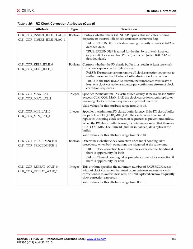
Spartan-6 FPGA GTP Transceivers (Advance Spec) www.xilinx.com 145UG386 (v2.2) April 30, 2010
RX Clock Correction
CLK_COR_INSERT_IDLE_FLAG_0
CLK_COR_INSERT_IDLE_FLAG_1
Boolean Controls whether the RXRUNDISP input status indicates running disparity or inserted-idle (clock correction sequence) flag.
FALSE: RXRUNDISP indicates running disparity when RXDATA is decoded data.
TRUE: RXRUNDISP is raised for the first byte of each inserted (repeated) clock correction (“Idle”) sequence (when RXDATA is decoded data).
CLK_COR_KEEP_IDLE_0
CLK_COR_KEEP_IDLE_1
Boolean Controls whether the RX elastic buffer must retain at least one clock correction sequence in the byte stream.
FALSE: The transceiver can remove all clock correction sequences to further re-center the RX elastic buffer during clock correction.
TRUE: In the final RXDATA stream, the transceiver must leave at least one clock correction sequence per continuous stream of clock correction sequences.
CLK_COR_MAX_LAT_0
CLK_COR_MAX_LAT_1
Integer Specifies the maximum RX elastic buffer latency. If the RX elastic buffer exceeds CLK_COR_MAX_LAT, the clock correction circuit replicates incoming clock correction sequences to prevent overflow.
Valid values for this attribute range from 3 to 48.
CLK_COR_MIN_LAT_0
CLK_COR_MIN_LAT_1
Integer Specifies the minimum RX elastic buffer latency. If the RX elastic buffer drops below CLK_COR_MIN_LAT, the clock correction circuit replicates incoming clock correction sequences to prevent underflow.
When the RX elastic buffer is reset, its pointers are set so that there are CLK_COR_MIN_LAT unread (and un-initialized) data bytes in the buffer.
Valid values for this attribute range from 3 to 48.
CLK_COR_PRECEDENCE_0
CLK_COR_PRECEDENCE_1
Boolean Determines whether clock correction or channel bonding takes precedence when both operations are triggered at the same time.
TRUE: Clock correction takes precedence over channel bonding if there is opportunity for both
FALSE: Channel bonding takes precedence over clock correction if there is opportunity for both
CLK_COR_REPEAT_WAIT_0
CLK_COR_REPEAT_WAIT_1
Integer This attribute specifies the minimum number of RXUSRCLK cycles without clock correction that must occur between successive clock corrections. If this attribute is zero, no limit is placed on how frequently clock correction can occur.
Valid values for this attribute range from 0 to 31.
Table 4-35: RX Clock Correction Attributes (Cont’d)
Attribute Type Description
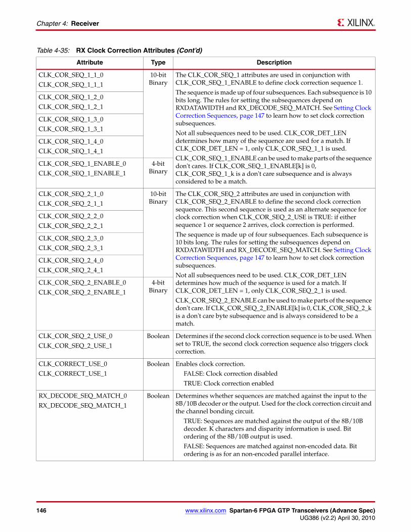
146 www.xilinx.com Spartan-6 FPGA GTP Transceivers (Advance Spec)UG386 (v2.2) April 30, 2010
Chapter 4: Receiver
CLK_COR_SEQ_1_1_0
CLK_COR_SEQ_1_1_1
10-bit Binary
The CLK_COR_SEQ_1 attributes are used in conjunction with CLK_COR_SEQ_1_ENABLE to define clock correction sequence 1.
The sequence is made up of four subsequences. Each subsequence is 10 bits long. The rules for setting the subsequences depend on RXDATAWIDTH and RX_DECODE_SEQ_MATCH. See Setting Clock Correction Sequences, page 147 to learn how to set clock correction subsequences.
Not all subsequences need to be used. CLK_COR_DET_LEN determines how many of the sequence are used for a match. If CLK_COR_DET_LEN = 1, only CLK_COR_SEQ_1_1 is used.
CLK_COR_SEQ_1_ENABLE can be used to make parts of the sequence don't cares. If CLK_COR_SEQ_1_ENABLE[k] is 0, CLK_COR_SEQ_1_k is a don't care subsequence and is always considered to be a match.
CLK_COR_SEQ_1_2_0
CLK_COR_SEQ_1_2_1
CLK_COR_SEQ_1_3_0
CLK_COR_SEQ_1_3_1
CLK_COR_SEQ_1_4_0
CLK_COR_SEQ_1_4_1
CLK_COR_SEQ_1_ENABLE_0
CLK_COR_SEQ_1_ENABLE_1
4-bit Binary
CLK_COR_SEQ_2_1_0
CLK_COR_SEQ_2_1_1
10-bit Binary
The CLK_COR_SEQ_2 attributes are used in conjunction with CLK_COR_SEQ_2_ENABLE to define the second clock correction sequence. This second sequence is used as an alternate sequence for clock correction when CLK_COR_SEQ_2_USE is TRUE: if either sequence 1 or sequence 2 arrives, clock correction is performed.
The sequence is made up of four subsequences. Each subsequence is 10 bits long. The rules for setting the subsequences depend on RXDATAWIDTH and RX_DECODE_SEQ_MATCH. See Setting Clock Correction Sequences, page 147 to learn how to set clock correction subsequences.
Not all subsequences need to be used. CLK_COR_DET_LEN determines how much of the sequence is used for a match. If CLK_COR_DET_LEN = 1, only CLK_COR_SEQ_2_1 is used.
CLK_COR_SEQ_2_ENABLE can be used to make parts of the sequence don't care. If CLK_COR_SEQ_2_ENABLE[k] is 0, CLK_COR_SEQ_2_k is a don't care byte subsequence and is always considered to be a match.
CLK_COR_SEQ_2_2_0
CLK_COR_SEQ_2_2_1
CLK_COR_SEQ_2_3_0
CLK_COR_SEQ_2_3_1
CLK_COR_SEQ_2_4_0
CLK_COR_SEQ_2_4_1
CLK_COR_SEQ_2_ENABLE_0
CLK_COR_SEQ_2_ENABLE_1
4-bit Binary
CLK_COR_SEQ_2_USE_0
CLK_COR_SEQ_2_USE_1
Boolean Determines if the second clock correction sequence is to be used. When set to TRUE, the second clock correction sequence also triggers clock correction.
CLK_CORRECT_USE_0
CLK_CORRECT_USE_1
Boolean Enables clock correction.
FALSE: Clock correction disabled
TRUE: Clock correction enabled
RX_DECODE_SEQ_MATCH_0
RX_DECODE_SEQ_MATCH_1
Boolean Determines whether sequences are matched against the input to the 8B/10B decoder or the output. Used for the clock correction circuit and the channel bonding circuit.
TRUE: Sequences are matched against the output of the 8B/10B decoder. K characters and disparity information is used. Bit ordering of the 8B/10B output is used.
FALSE: Sequences are matched against non-encoded data. Bit ordering is as for an non-encoded parallel interface.
Table 4-35: RX Clock Correction Attributes (Cont’d)
Attribute Type Description
Spartan-6 FPGA GTP Transceivers (Advance Spec) www.xilinx.com 147UG386 (v2.2) April 30, 2010
RX Clock Correction
Using RX Clock CorrectionThe user must follow the steps described in this section to use the receiver clock correction.
Enabling Clock Correction
Each GTP transceiver includes a clock correction circuit that performs clock correction by controlling the pointers of the RX elastic buffer. To use clock correction, RX_BUFFER_USE is set to TRUE to turn on the RX elastic buffer, and CLK_CORRECT_USE is set to TRUE to turn on the clock correction circuit.
Clock correction is triggered when the RX elastic buffer latency is too high or too low, and the clock correction circuit detects a match sequence. To use clock correction, the clock correction circuit must be configured to set the following items:
• RX elastic buffer limits
• Clock correction sequence
Setting RX Elastic Buffer Limits
The RX elastic buffer limits are set using CLK_COR_MIN_LAT (minimum latency) and CLK_COR_MAX_LAT (maximum latency). When the number of bytes in the RX elastic buffer drops below CLK_COR_MIN_LAT, the clock correction circuit writes an additional CLK_COR_ADJ_LEN bytes from the first clock correction sequence it matches to prevent the buffer from underflowing. Similarly, when the number of bytes in the RX elastic buffer exceeds CLK_COR_MAX_LAT, the clock correction circuit deletes CLK_COR_ADJ_LEN bytes from the first clock correction sequence it matches, starting with the first byte of the sequence.
Setting Clock Correction Sequences
The clock correction sequences are programmed using the CLK_COR_SEQ_1_* attributes and CLK_COR_ADJ_LEN. Each CLK_COR_SEQ_1_* attribute corresponds to one subsequence in clock correction sequence 1. CLK_COR_ADJ_LEN is used to set the number of subsequences to be matched. If the 20-bit internal datapath is used, the clock correction circuit matches all 10 bits of each subsequence. If the 16-bit internal datapath is used, only the right-most eight bits of each subsequence are used.
A second, alternate clock correction sequence can be activated by setting CLK_COR_SEQ_2_USE to TRUE. The first and second sequences share length settings, but use different subsequence values for matching. Set the CLK_COR_SEQ_2_* attributes to define the subsequence values for the second sequence.
When using 8B/10B decoding (RXDEC8B10BUSE is High), RX_DECODE_SEQ_MATCH is set to TRUE to search the output of the 8B/10B decoder for sequence matches instead of non-decoded data. This allows the circuit to look for 8-bit values with either positive or negative disparity, and to distinguish K characters from regular characters (see TX 8B/10B Encoder, page 75 and RX 8B/10B Decoder, page 130 for details). Figure 4-28 shows how to set a clock correction sequence byte when RX_DECODE_SEQ_MATCH is TRUE.
When RX_DECODE_SEQ_MATCH is FALSE, the sequence must exactly match non-encoded incoming data.
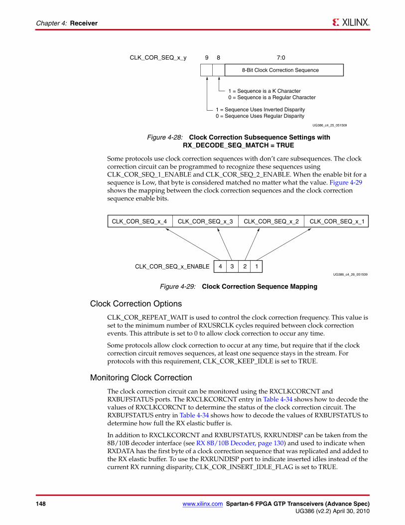
148 www.xilinx.com Spartan-6 FPGA GTP Transceivers (Advance Spec)UG386 (v2.2) April 30, 2010
Chapter 4: Receiver
Some protocols use clock correction sequences with don’t care subsequences. The clock correction circuit can be programmed to recognize these sequences using CLK_COR_SEQ_1_ENABLE and CLK_COR_SEQ_2_ENABLE. When the enable bit for a sequence is Low, that byte is considered matched no matter what the value. Figure 4-29 shows the mapping between the clock correction sequences and the clock correction sequence enable bits.
Clock Correction Options
CLK_COR_REPEAT_WAIT is used to control the clock correction frequency. This value is set to the minimum number of RXUSRCLK cycles required between clock correction events. This attribute is set to 0 to allow clock correction to occur any time.
Some protocols allow clock correction to occur at any time, but require that if the clock correction circuit removes sequences, at least one sequence stays in the stream. For protocols with this requirement, CLK_COR_KEEP_IDLE is set to TRUE.
Monitoring Clock Correction
The clock correction circuit can be monitored using the RXCLKCORCNT and RXBUFSTATUS ports. The RXCLKCORCNT entry in Table 4-34 shows how to decode the values of RXCLKCORCNT to determine the status of the clock correction circuit. The RXBUFSTATUS entry in Table 4-34 shows how to decode the values of RXBUFSTATUS to determine how full the RX elastic buffer is.
In addition to RXCLKCORCNT and RXBUFSTATUS, RXRUNDISP can be taken from the 8B/10B decoder interface (see RX 8B/10B Decoder, page 130) and used to indicate when RXDATA has the first byte of a clock correction sequence that was replicated and added to the RX elastic buffer. To use the RXRUNDISP port to indicate inserted idles instead of the current RX running disparity, CLK_COR_INSERT_IDLE_FLAG is set to TRUE.
X-Ref Target - Figure 4-28
Figure 4-28: Clock Correction Subsequence Settings with RX_DECODE_SEQ_MATCH = TRUE
X-Ref Target - Figure 4-29
Figure 4-29: Clock Correction Sequence Mapping
8-Bit Clock Correction Sequence
1 = Sequence is a K Character0 = Sequence is a Regular Character
1 = Sequence Uses Inverted Disparity0 = Sequence Uses Regular Disparity
7:0
UG386_c4_25_051509
89CLK_COR_SEQ_x_y
UG386_c4_26_051509
34 12
CLK_COR_SEQ_x_4 CLK_COR_SEQ_x_3 CLK_COR_SEQ_x_2
CLK_COR_SEQ_x_ENABLE
CLK_COR_SEQ_x_1
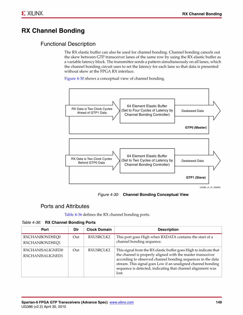
Spartan-6 FPGA GTP Transceivers (Advance Spec) www.xilinx.com 149UG386 (v2.2) April 30, 2010
RX Channel Bonding
RX Channel Bonding
Functional DescriptionThe RX elastic buffer can also be used for channel bonding. Channel bonding cancels out the skew between GTP transceiver lanes of the same row by using the RX elastic buffer as a variable latency block. The transmitter sends a pattern simultaneously on all lanes, which the channel bonding circuit uses to set the latency for each lane so that data is presented without skew at the FPGA RX interface.
Figure 4-30 shows a conceptual view of channel bonding.
Ports and AttributesTable 4-36 defines the RX channel bonding ports.
X-Ref Target - Figure 4-30
Figure 4-30: Channel Bonding Conceptual View
Deskewed DataRX Data is Two Clock Cycles
Behind GTP0 Data
64 Element Elastic Buffer(Set to Two Cycles of Latency by
Channel Bonding Controller)
UG386_c4_27_052609
GTP1 (Slave)
Deskewed DataRX Data is Two Clock Cycles
Ahead of GTP1 Data
64 Element Elastic Buffer(Set to Four Cycles of Latency by
Channel Bonding Controller)
GTP0 (Master)
Table 4-36: RX Channel Bonding Ports
Port Dir Clock Domain Description
RXCHANBONDSEQ0
RXCHANBONDSEQ1
Out RXUSRCLK2 This port goes High when RXDATA contains the start of a channel bonding sequence.
RXCHANISALIGNED0
RXCHANISALIGNED1
Out RXUSRCLK2 This signal from the RX elastic buffer goes High to indicate that the channel is properly aligned with the master transceiver according to observed channel bonding sequences in the data stream. This signal goes Low if an unaligned channel bonding sequence is detected, indicating that channel alignment was lost.
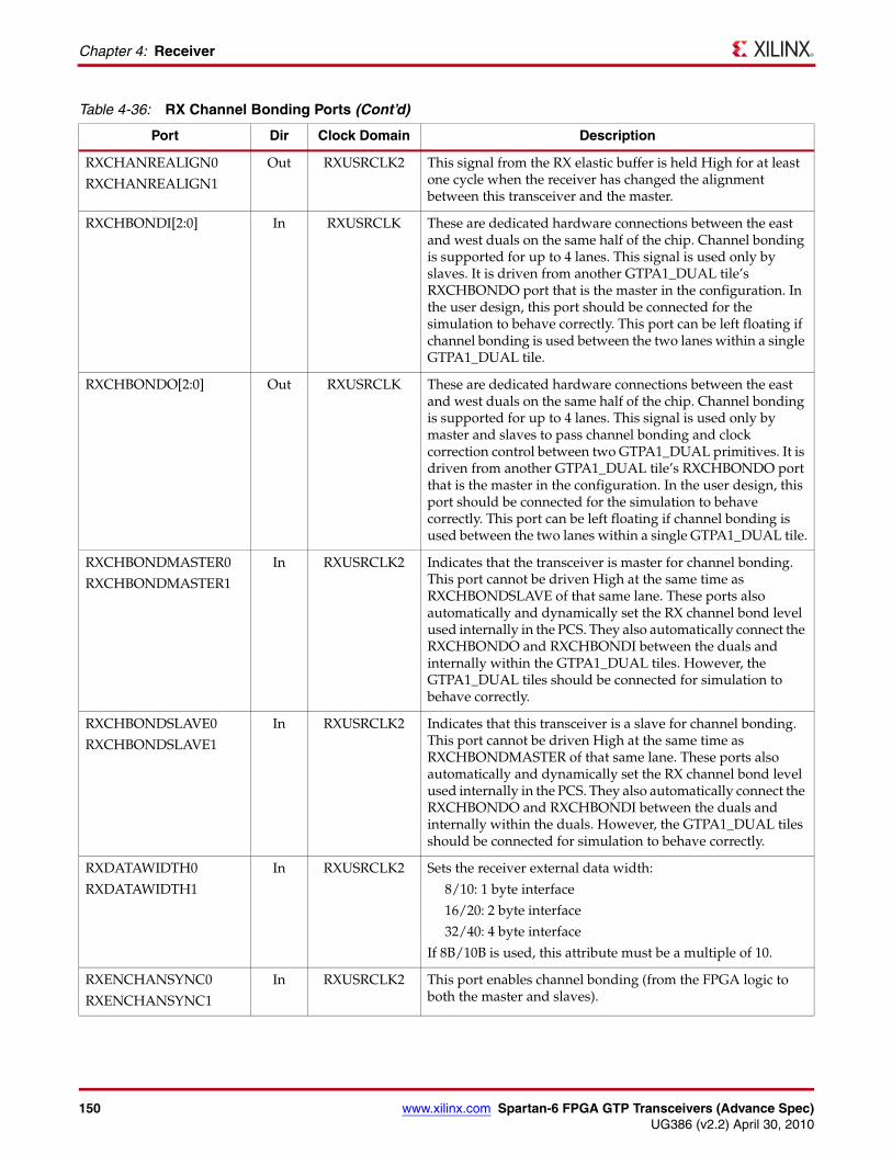
150 www.xilinx.com Spartan-6 FPGA GTP Transceivers (Advance Spec)UG386 (v2.2) April 30, 2010
Chapter 4: Receiver
RXCHANREALIGN0
RXCHANREALIGN1
Out RXUSRCLK2 This signal from the RX elastic buffer is held High for at least one cycle when the receiver has changed the alignment between this transceiver and the master.
RXCHBONDI[2:0] In RXUSRCLK These are dedicated hardware connections between the east and west duals on the same half of the chip. Channel bonding is supported for up to 4 lanes. This signal is used only by slaves. It is driven from another GTPA1_DUAL tile’s RXCHBONDO port that is the master in the configuration. In the user design, this port should be connected for the simulation to behave correctly. This port can be left floating if channel bonding is used between the two lanes within a single GTPA1_DUAL tile.
RXCHBONDO[2:0] Out RXUSRCLK These are dedicated hardware connections between the east and west duals on the same half of the chip. Channel bonding is supported for up to 4 lanes. This signal is used only by master and slaves to pass channel bonding and clock correction control between two GTPA1_DUAL primitives. It is driven from another GTPA1_DUAL tile’s RXCHBONDO port that is the master in the configuration. In the user design, this port should be connected for the simulation to behave correctly. This port can be left floating if channel bonding is used between the two lanes within a single GTPA1_DUAL tile.
RXCHBONDMASTER0
RXCHBONDMASTER1
In RXUSRCLK2 Indicates that the transceiver is master for channel bonding. This port cannot be driven High at the same time as RXCHBONDSLAVE of that same lane. These ports also automatically and dynamically set the RX channel bond level used internally in the PCS. They also automatically connect the RXCHBONDO and RXCHBONDI between the duals and internally within the GTPA1_DUAL tiles. However, the GTPA1_DUAL tiles should be connected for simulation to behave correctly.
RXCHBONDSLAVE0
RXCHBONDSLAVE1
In RXUSRCLK2 Indicates that this transceiver is a slave for channel bonding. This port cannot be driven High at the same time as RXCHBONDMASTER of that same lane. These ports also automatically and dynamically set the RX channel bond level used internally in the PCS. They also automatically connect the RXCHBONDO and RXCHBONDI between the duals and internally within the duals. However, the GTPA1_DUAL tiles should be connected for simulation to behave correctly.
RXDATAWIDTH0
RXDATAWIDTH1
In RXUSRCLK2 Sets the receiver external data width:
8/10: 1 byte interface
16/20: 2 byte interface
32/40: 4 byte interface
If 8B/10B is used, this attribute must be a multiple of 10.
RXENCHANSYNC0
RXENCHANSYNC1
In RXUSRCLK2 This port enables channel bonding (from the FPGA logic to both the master and slaves).
Table 4-36: RX Channel Bonding Ports (Cont’d)
Port Dir Clock Domain Description
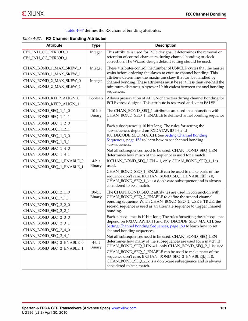
Spartan-6 FPGA GTP Transceivers (Advance Spec) www.xilinx.com 151UG386 (v2.2) April 30, 2010
RX Channel Bonding
Table 4-37 defines the RX channel bonding attributes.
Table 4-37: RX Channel Bonding Attributes
Attribute Type Description
CB2_INH_CC_PERIOD_0
CB2_INH_CC_PERIOD_1
Integer This attribute is used for PCIe designs. It determines the removal or retention of control characters during channel bonding or clock correction. The Wizard design default setting should be used.
CHAN_BOND_1_MAX_SKEW_0
CHAN_BOND_1_MAX_SKEW_1
Integer These attributes control the number of USRCLK cycles that the master waits before ordering the slaves to execute channel bonding. This attribute determines the maximum skew that can be handled by channel bonding. These attributes must be set at less than one-half the minimum distance (in bytes or 10-bit codes) between channel bonding sequences.
CHAN_BOND_2_MAX_SKEW_0
CHAN_BOND_2_MAX_SKEW_1
Integer
CHAN_BOND_KEEP_ALIGN_0
CHAN_BOND_KEEP_ALIGN_1
Boolean Allows preservation of ALIGN characters during channel bonding for PCI Express designs. This attribute is reserved and set to FALSE.
CHAN_BOND_SEQ_1_1_0
CHAN_BOND_SEQ_1_1_1
10-bit Binary
The CHAN_BOND_SEQ_1 attributes are used in conjunction with CHAN_BOND_SEQ_1_ENABLE to define channel bonding sequence 1.
Each subsequence is 10 bits long. The rules for setting the subsequences depend on RXDATAWIDTH and RX_DECODE_SEQ_MATCH. See Setting Channel Bonding Sequences, page 153 to learn how to set channel bonding subsequences.
Not all subsequences need to be used. CHAN_BOND_SEQ_LEN determines how much of the sequence is used for a match.
If CHAN_BOND_SEQ_LEN = 1, only CHAN_BOND_SEQ_1_1 is used.
CHAN_BOND_SEQ_1_ENABLE can be used to make parts of the sequence don't care. If CHAN_BOND_SEQ_1_ENABLE[k] is 0, CHAN_BOND_SEQ_1_k is a don't-care subsequence and is always considered to be a match.
CHAN_BOND_SEQ_1_2_0
CHAN_BOND_SEQ_1_2_1
CHAN_BOND_SEQ_1_3_0
CHAN_BOND_SEQ_1_3_1
CHAN_BOND_SEQ_1_4_0
CHAN_BOND_SEQ_1_4_1
CHAN_BOND_SEQ_1_ENABLE_0
CHAN_BOND_SEQ_1_ENABLE_1
4-bit Binary
CHAN_BOND_SEQ_2_1_0
CHAN_BOND_SEQ_2_1_1
10-bit Binary
The CHAN_BOND_SEQ_2 attributes are used in conjunction with CHAN_BOND_SEQ_2_ENABLE to define the second channel bonding sequence. When CHAN_BOND_SEQ_2_USE is TRUE, the second sequence is used as an alternate sequence to trigger channel bonding.
Each subsequence is 10 bits long. The rules for setting the subsequence depend on RXDATAWIDTH and RX_DECODE_SEQ_MATCH. See Setting Channel Bonding Sequences, page 153 to learn how to set channel bonding sequences.
Not all subsequences need to be used. CHAN_BOND_SEQ_LEN determines how many of the subsequences are used for a match. If CHAN_BOND_SEQ_LEN = 1, only CHAN_BOND_SEQ_2_1 is used.
CHAN_BOND_SEQ_2_ENABLE can be used to make parts of the sequence don't care. If CHAN_BOND_SEQ_2_ENABLE[k] is 0, CHAN_BOND_SEQ_2_k is a don't-care subsequence and is always considered to be a match.
CHAN_BOND_SEQ_2_2_0
CHAN_BOND_SEQ_2_2_1
CHAN_BOND_SEQ_2_3_0
CHAN_BOND_SEQ_2_3_1
CHAN_BOND_SEQ_2_4_0
CHAN_BOND_SEQ_2_4_1
CHAN_BOND_SEQ_2_ENABLE_0
CHAN_BOND_SEQ_2_ENABLE_1
4-bit Binary
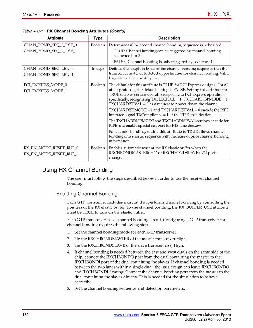
152 www.xilinx.com Spartan-6 FPGA GTP Transceivers (Advance Spec)UG386 (v2.2) April 30, 2010
Chapter 4: Receiver
Using RX Channel BondingThe user must follow the steps described below in order to use the receiver channel bonding.
Enabling Channel Bonding
Each GTP transceiver includes a circuit that performs channel bonding by controlling the pointers of the RX elastic buffer. To use channel bonding, the RX_BUFFER_USE attribute must be TRUE to turn on the elastic buffer.
Each GTP transceiver has a channel bonding circuit. Configuring a GTP transceiver for channel bonding requires the following steps:
1. Set the channel bonding mode for each GTP transceiver.
2. Tie the RXCHBONDMASTER of the master transceiver High.
3. Tie the RXCHBONDSLAVE of the slave transceiver(s) High.
4. If channel bonding is needed between the east and west duals on the same side of the chip, connect the RXCHBONDO port from the dual containing the master to the RXCHBONDI port of the dual containing the slaves. If channel bonding is needed between the two lanes within a single dual, the user design can leave RXCHBONDO and RXCHBONDI floating. Connect the channel bonding port from the master to the dual containing the slaves directly. This is needed for the simulation to behave correctly.
5. Set the channel bonding sequence and detection parameters.
CHAN_BOND_SEQ_2_USE_0
CHAN_BOND_SEQ_2_USE_1
Boolean Determines if the second channel bonding sequence is to be used.
TRUE: Channel bonding can be triggered by channel bonding sequence 1 or 2.
FALSE: Channel bonding is only triggered by sequence 1.
CHAN_BOND_SEQ_LEN_0
CHAN_BOND_SEQ_LEN_1
Integer Defines the length in bytes of the channel bonding sequence that the transceiver matches to detect opportunities for channel bonding. Valid lengths are 1, 2, and 4 bytes.
PCI_EXPRESS_MODE_0
PCI_EXPRESS_MODE_1
Boolean The default for this attribute is TRUE for PCI Express designs. For all other protocols, the default setting is FALSE. Setting this attribute to TRUE enables certain operations specific to PCI Express operation, specifically, recognizing TXELECIDLE = 1, TXCHARDISPMODE = 1, TXCHARDISPVAL = 0 as a request to power down the channel.
TXCHARDISPMODE = 1 and TXCHARDISPVAL = 0 encode the PIPE interface signal TXCompliance = 1 of the PIPE specification.
The TXCHARDISPMODE and TXCHARDISPVAL settings encode for PIPE and enable special support for FTS lane deskew.
For channel bonding, setting this attribute to TRUE allows channel bonding on a shorter sequence with the reuse of prior channel bonding information.
RX_EN_MODE_RESET_BUF_0
RX_EN_MODE_RESET_BUF_1
Boolean Enables automatic reset of the RX elastic buffer when the RXCHBONDMASTER(0/1) or RXCHBONDSLAVE(0/1) ports change.
Table 4-37: RX Channel Bonding Attributes (Cont’d)
Attribute Type Description
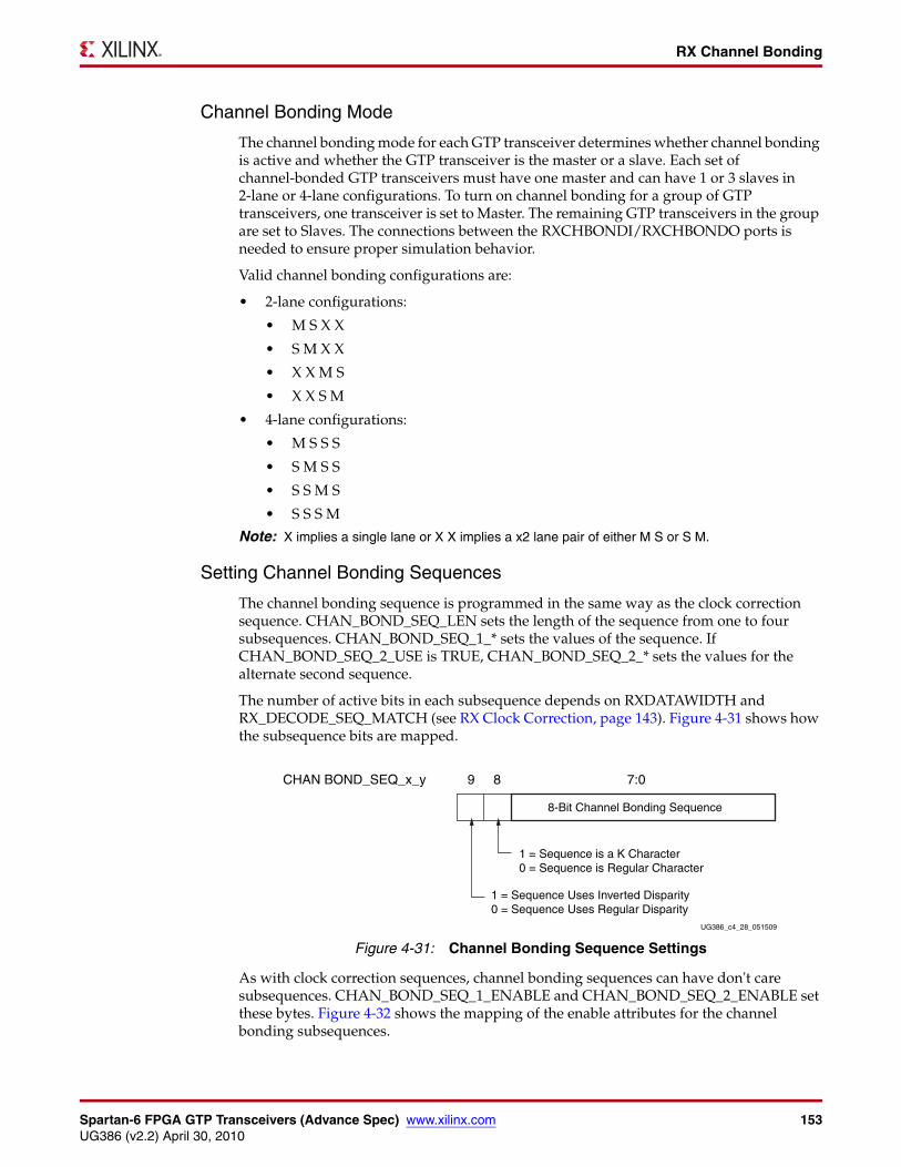
Spartan-6 FPGA GTP Transceivers (Advance Spec) www.xilinx.com 153UG386 (v2.2) April 30, 2010
RX Channel Bonding
Channel Bonding Mode
The channel bonding mode for each GTP transceiver determines whether channel bonding is active and whether the GTP transceiver is the master or a slave. Each set of channel-bonded GTP transceivers must have one master and can have 1 or 3 slaves in 2-lane or 4-lane configurations. To turn on channel bonding for a group of GTP transceivers, one transceiver is set to Master. The remaining GTP transceivers in the group are set to Slaves. The connections between the RXCHBONDI/RXCHBONDO ports is needed to ensure proper simulation behavior.
Valid channel bonding configurations are:
• 2-lane configurations:
• M S X X
• S M X X
• X X M S
• X X S M
• 4-lane configurations:
• M S S S
• S M S S
• S S M S
• S S S M
Note: X implies a single lane or X X implies a x2 lane pair of either M S or S M.
Setting Channel Bonding Sequences
The channel bonding sequence is programmed in the same way as the clock correction sequence. CHAN_BOND_SEQ_LEN sets the length of the sequence from one to four subsequences. CHAN_BOND_SEQ_1_* sets the values of the sequence. If CHAN_BOND_SEQ_2_USE is TRUE, CHAN_BOND_SEQ_2_* sets the values for the alternate second sequence.
The number of active bits in each subsequence depends on RXDATAWIDTH and RX_DECODE_SEQ_MATCH (see RX Clock Correction, page 143). Figure 4-31 shows how the subsequence bits are mapped.
As with clock correction sequences, channel bonding sequences can have don't care subsequences. CHAN_BOND_SEQ_1_ENABLE and CHAN_BOND_SEQ_2_ENABLE set these bytes. Figure 4-32 shows the mapping of the enable attributes for the channel bonding subsequences.
X-Ref Target - Figure 4-31
Figure 4-31: Channel Bonding Sequence Settings
8-Bit Channel Bonding Sequence
1 = Sequence is a K Character0 = Sequence is Regular Character
1 = Sequence Uses Inverted Disparity0 = Sequence Uses Regular Disparity
7:0
UG386_c4_28_051509
89CHAN BOND_SEQ_x_y
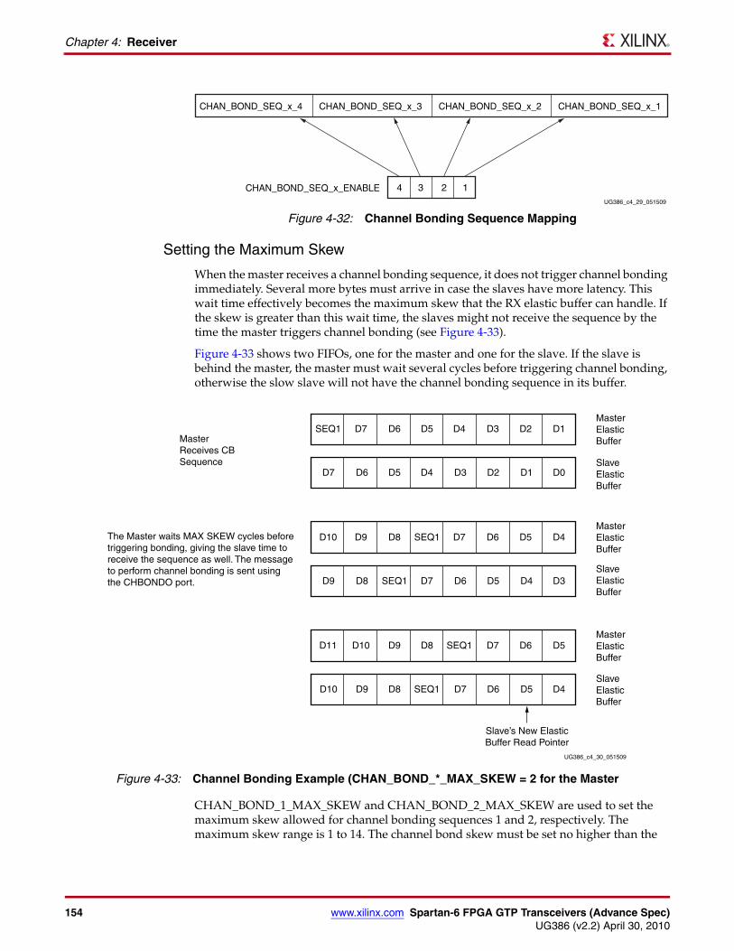
154 www.xilinx.com Spartan-6 FPGA GTP Transceivers (Advance Spec)UG386 (v2.2) April 30, 2010
Chapter 4: Receiver
Setting the Maximum Skew
When the master receives a channel bonding sequence, it does not trigger channel bonding immediately. Several more bytes must arrive in case the slaves have more latency. This wait time effectively becomes the maximum skew that the RX elastic buffer can handle. If the skew is greater than this wait time, the slaves might not receive the sequence by the time the master triggers channel bonding (see Figure 4-33).
Figure 4-33 shows two FIFOs, one for the master and one for the slave. If the slave is behind the master, the master must wait several cycles before triggering channel bonding, otherwise the slow slave will not have the channel bonding sequence in its buffer.
CHAN_BOND_1_MAX_SKEW and CHAN_BOND_2_MAX_SKEW are used to set the maximum skew allowed for channel bonding sequences 1 and 2, respectively. The maximum skew range is 1 to 14. The channel bond skew must be set no higher than the
X-Ref Target - Figure 4-32
Figure 4-32: Channel Bonding Sequence Mapping
UG386_c4_29_051509
34 12
CHAN_BOND_SEQ_x_4 CHAN_BOND_SEQ_x_3 CHAN_BOND_SEQ_x_2
CHAN_BOND_SEQ_x_ENABLE
CHAN_BOND_SEQ_x_1
X-Ref Target - Figure 4-33
Figure 4-33: Channel Bonding Example (CHAN_BOND_*_MAX_SKEW = 2 for the Master
The Master waits MAX SKEW cycles beforetriggering bonding, giving the slave time toreceive the sequence as well. The messageto perform channel bonding is sent usingthe CHBONDO port.
MasterReceives CBSequence
MasterElasticBuffer
SlaveElasticBuffer
MasterElasticBuffer
SlaveElasticBuffer
MasterElasticBuffer
SlaveElasticBuffer
UG386_c4_30_051509
Slave’s New ElasticBuffer Read Pointer
D1D2D3D4D5D6D7SEQ1
D1D2D3D4D5D6D7 D0
D4D5D6D7SEQ1D8D9D10
D4D5D6D7SEQ1D8D9 D3
D5D6D7SEQ1D8D9D10D11
D5D6D7SEQ1D8D9D10 D4
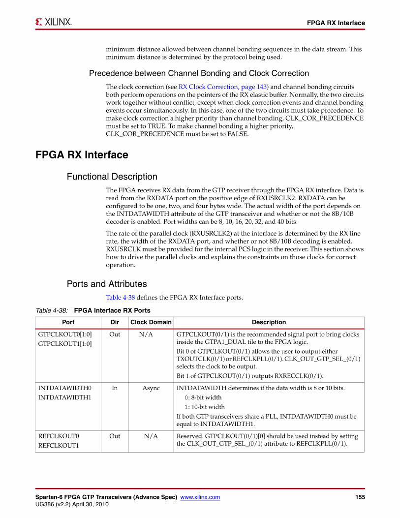
Spartan-6 FPGA GTP Transceivers (Advance Spec) www.xilinx.com 155UG386 (v2.2) April 30, 2010
FPGA RX Interface
minimum distance allowed between channel bonding sequences in the data stream. This minimum distance is determined by the protocol being used.
Precedence between Channel Bonding and Clock Correction
The clock correction (see RX Clock Correction, page 143) and channel bonding circuits both perform operations on the pointers of the RX elastic buffer. Normally, the two circuits work together without conflict, except when clock correction events and channel bonding events occur simultaneously. In this case, one of the two circuits must take precedence. To make clock correction a higher priority than channel bonding, CLK_COR_PRECEDENCE must be set to TRUE. To make channel bonding a higher priority, CLK_COR_PRECEDENCE must be set to FALSE.
FPGA RX Interface
Functional DescriptionThe FPGA receives RX data from the GTP receiver through the FPGA RX interface. Data is read from the RXDATA port on the positive edge of RXUSRCLK2. RXDATA can be configured to be one, two, and four bytes wide. The actual width of the port depends on the INTDATAWIDTH attribute of the GTP transceiver and whether or not the 8B/10B decoder is enabled. Port widths can be 8, 10, 16, 20, 32, and 40 bits.
The rate of the parallel clock (RXUSRCLK2) at the interface is determined by the RX line rate, the width of the RXDATA port, and whether or not 8B/10B decoding is enabled. RXUSRCLK must be provided for the internal PCS logic in the receiver. This section shows how to drive the parallel clocks and explains the constraints on those clocks for correct operation.
Ports and AttributesTable 4-38 defines the FPGA RX Interface ports.
Table 4-38: FPGA Interface RX Ports
Port Dir Clock Domain Description
GTPCLKOUT0[1:0]
GTPCLKOUT1[1:0]
Out N/A GTPCLKOUT(0/1) is the recommended signal port to bring clocks inside the GTPA1_DUAL tile to the FPGA logic.
Bit 0 of GTPCLKOUT(0/1) allows the user to output either TXOUTCLK(0/1) or REFCLKPLL(0/1). CLK_OUT_GTP_SEL_(0/1) selects the clock to be output.
Bit 1 of GTPCLKOUT(0/1) outputs RXRECCLK(0/1).
INTDATAWIDTH0
INTDATAWIDTH1
In Async INTDATAWIDTH determines if the data width is 8 or 10 bits.
0: 8-bit width
1: 10-bit width
If both GTP transceivers share a PLL, INTDATAWIDTH0 must be equal to INTDATAWIDTH1.
REFCLKOUT0
REFCLKOUT1
Out N/A Reserved. GTPCLKOUT(0/1)[0] should be used instead by setting the CLK_OUT_GTP_SEL_(0/1) attribute to REFCLKPLL(0/1).
156 www.xilinx.com Spartan-6 FPGA GTP Transceivers (Advance Spec)UG386 (v2.2) April 30, 2010
Chapter 4: Receiver
There are no FPGA RX interface attributes.
DescriptionThe FPGA RX interface allows parallel received data to be read from the GTP transceiver. For this interface to be used, the following must be done:
• The width of the RXDATA port must be configured
• RXUSRCLK2 and RXUSRCLK must be connected to clocks running at the correct rate
RXDATA0[31:0]
RXDATA1[31:0]
Out RXUSRCLK2 This output is the receive data bus of the receive interface to the FPGA. The width of RXDATA(0/1) depends on the setting of RXDATAWIDTH(0/1).
RXDATAWIDTH0
RXDATAWIDTH1
In RXUSRCLK2 This port selects the width of the RXDATA(0/1) receive data connection to the FPGA.
0: One-byte interface → RXDATA(0/1)[7:0]
1: Two-byte interface → RXDATA(0/1)[15:0]
2: Four-byte interface → RXDATA(0/1)[31:0]
The clock domain depends on the selected clock [RXRECCLK(0/1), RXUSRCLK(0/1), and RXUSRCLK2(0/1)] for this interface.
RXRECCLK0
RXRECCLK1
Out N/A This port is the recovered clock from the CDR. It clocks the RX logic between the PMA and the RX elastic buffer. This clock can be used to drive RXUSRCLK synchronously with incoming data.
When RXPOWERDOWN[1:0] is set to 11, which is P2 (the lowest power state), the RXRECCLK of this transceiver is indeterminate. RXRECCLK of this GTP transceiver is either a static 1 or a static 0.
RXRESET0
RXRESET1
In Async This port is the PCS RX system reset. It resets the RX elastic buffer, the 8B/10B decoder, comma detect, and other RX registers. RXRESET is a per channel subset of GTPRESET.
RXUSRCLK20(1)
RXUSRCLK21
In N/A This port synchronizes the FPGA logic with the RX interface. This clock must be positive-edge aligned to RXUSRCLK. The clock rate depends on FRXUSRCLK and RXDATAWIDTH:
RXDATAWIDTH = 0; FRXUSRCLK2 = FRXUSRCLK
RXDATAWIDTH = 1; FRXUSRCLK2 = FRXUSRCLK/2
RXDATAWIDTH = 2; FRXUSRCLK2 = FRXUSRCLK/4
RXUSRCLK0(1)
RXUSRCLK1
In N/A This port provides a clock for the internal RX PCS datapath. This clock must always be provided. The rate depends on INTDATAWIDTH(0/1) where:
INTDATAWIDTH(0/1) is Low; FRXUSRCLK = Line Rate/8
INTDATAWIDTH(0/1) is High; FRXUSRCLK = Line Rate/10
Notes: 1. Refer to the Spartan-6 FGPA Data Sheet for the frequency specification of RXUSRCLK and RXUSRCLK2.
Table 4-38: FPGA Interface RX Ports (Cont’d)
Port Dir Clock Domain Description
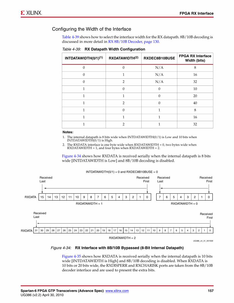
Spartan-6 FPGA GTP Transceivers (Advance Spec) www.xilinx.com 157UG386 (v2.2) April 30, 2010
FPGA RX Interface
Configuring the Width of the Interface
Table 4-39 shows how to select the interface width for the RX datapath. 8B/10B decoding is discussed in more detail in RX 8B/10B Decoder, page 130.
Figure 4-34 shows how RXDATA is received serially when the internal datapath is 8 bits wide [INTDATAWIDTH is Low] and 8B/10B decoding is disabled.
Figure 4-35 shows how RXDATA is received serially when the internal datapath is 10 bits wide [INTDATAWIDTH is High] and 8B/10B decoding is disabled. When RXDATA is 10 bits or 20 bits wide, the RXDISPERR and RXCHARISK ports are taken from the 8B/10B decoder interface and are used to present the extra bits.
Table 4-39: RX Datapath Width Configuration
INTDATAWIDTH(0/1)(1) RXDATAWIDTH(2) RXDEC8B10BUSEFPGA RX Interface
Width (bits)
0 0 N/A 8
0 1 N/A 16
0 2 N/A 32
1 0 0 10
1 1 0 20
1 2 0 40
1 0 1 8
1 1 1 16
1 2 1 32
Notes: 1. The internal datapath is 8 bits wide when INTDATAWIDTH(0/1) is Low and 10 bits when
INTDATAWIDTH(0/1) is High.2. The RXDATA interface is one byte wide when RXDATAWIDTH = 0, two bytes wide when
RXDATAWIDTH = 1, and four bytes when RXDATAWIDTH = 2.
X-Ref Target - Figure 4-34
Figure 4-34: RX Interface with 8B/10B Bypassed (8-Bit Internal Datapath)
15 14 13 12 11 10 9 8 7 6 5 4 3 2 1 0 7 6 5 4 3 2 1 0
RXDATAWIDTH = 1
INTDATAWIDTH(0/1) = 0 and RXDEC8B10BUSE = 0
RXDATA
RXDATA
RXDATAWIDTH = 0
UG386_c4_31_051509
ReceivedLast
ReceivedLast
ReceivedFirst
ReceivedFirst
15 14 13 12 11 10 9 8 7 6 5 4 3 2 1 0
RXDATAWIDTH = 2
ReceivedFirst
31 30 29 28 27 26 25 24 23 22 21 20 19 18 17 16
ReceivedLast
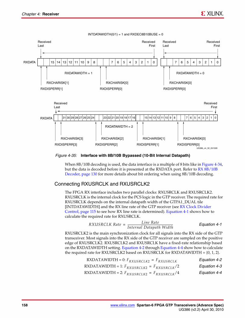
158 www.xilinx.com Spartan-6 FPGA GTP Transceivers (Advance Spec)UG386 (v2.2) April 30, 2010
Chapter 4: Receiver
When 8B/10B decoding is used, the data interface is a multiple of 8 bits like in Figure 4-34, but the data is decoded before it is presented at the RXDATA port. Refer to RX 8B/10B Decoder, page 130 for more details about bit ordering when using 8B/10B decoding.
Connecting RXUSRCLK and RXUSRCLK2
The FPGA RX interface includes two parallel clocks: RXUSRCLK and RXUSRCLK2. RXUSRCLK is the internal clock for the PCS logic in the GTP receiver. The required rate for RXUSRCLK depends on the internal datapath width of the GTPA1_DUAL tile [INTDATAWIDTH] and the RX line rate of the GTP receiver (see RX Clock Divider Control, page 115 to see how RX line rate is determined). Equation 4-1 shows how to calculate the required rate for RXUSRCLK.
Equation 4-1
RXUSRCLK2 is the main synchronization clock for all signals into the RX side of the GTP transceiver. Most signals into the RX side of the GTP receiver are sampled on the positive edge of RXUSRCLK2. RXUSRCLK2 and RXUSRCLK have a fixed-rate relationship based on the RXDATAWIDTH setting. Equation 4-2 through Equation 4-4 show how to calculate the required rate for RXUSRCLK2 based on RXUSRCLK for RXDATAWIDTH = {0, 1, 2}.
Equation 4-2
Equation 4-3
Equation 4-4
X-Ref Target - Figure 4-35
Figure 4-35: Interface with 8B/10B Bypassed (10-Bit Internal Datapath)
15 14 13 12 11 10 9 8 7 6 5 4 3 2 1 0 7 6 5 4 3 2 1 0
RXDATAWIDTH = 1
RXDATAWIDTH = 2
RXDATA
RXDATA
RXDATAWIDTH = 0
RXCHARISK[0]
RXDISPERR[0]
UG386_c4_32_051509
ReceivedLast
ReceivedLast
ReceivedFirst
ReceivedLast
ReceivedFirst
ReceivedFirst
RXCHARISK[0]
RXDISPERR[0]
RXCHARISK[1]
RXDISPERR[1]
RXCHARISK[0]
RXDISPERR[0]
RXCHARISK[1]
RXDISPERR[1]
RXCHARISK[2]
RXDISPERR[2]
RXCHARISK[3]
RXDISPERR[3]
INTDATAWIDTH(0/1) = 1 and RXDEC8B10BUSE = 0
15 14 13 12 11 10 9 8 7 6 5 4 3 2 1 023 22 21 161718192031 30 29 2425262728
RXUSRCLK Rate Line RateInternal Datapath Width--------------------------------------------------------------------=
RXDATAWIDTH = 0: FRXUSRCLK2 FRXUSRCLK=
RXDATAWIDTH = 1: FRXUSRCLK2 FRXUSRCLK/2=
RXDATAWIDTH = 2: FRXUSRCLK2 FRXUSRCLK/4=
Spartan-6 FPGA GTP Transceivers (Advance Spec) www.xilinx.com 159UG386 (v2.2) April 30, 2010
FPGA RX Interface
Some rules about the relationships between clocks must be observed for RXUSRCLK, RXUSRCLK2, and CLKIN:
• RXUSRCLK and RXUSRCLK2 must be positive-edge aligned, with as little skew as possible between them. Use low-skew clock resources (BUFGs) to drive RXUSRCLK and RXUSRCLK2. When the two are the same frequency, the same clock resource drives both. When the two are different frequencies, RXUSRCLK is divided to get RXUSRCLK2. The designer must ensure that the two are positive-edge aligned.
• If the channel is configured so that the same oscillator drives the reference clock for the transmitter and the receiver, GTPCLKOUT[0] can be used to drive RXUSRCLK and RXUSRCLK2 the same way that they are used to drive TXUSRCLK and TXUSRCLK2. (The user can set the CLK_OUT_GTP_SEL attribute to either TXOUTCLK or REFCLKPLL.) When clock correction is turned off, RX phase alignment must be used to align the serial clock and the parallel clocks. See RX Elastic Buffer Bypass, page 133 for details about enabling phase alignment.
• If separate oscillators are driving the reference clocks for the transmitter and receiver on the channel and clock correction is not used, RXUSRCLK and RXUSRCLK2 must be driven by GTPCLKOUT[1] (RXREFCLK), and the phase-alignment circuit must be used.
• If clock correction is used, RXUSRCLK and RXUSRCLK2 can be sourced by GTPCLKOUT[1] (RXREFCLK), GTPCLKOUT[0] (CLK_OUT_GTP_SEL attribute = "REFCLKPLL" or "TXOUTCLK").
• The GTPCLKOUT ports are connected to specific BUFIO2 primitives to access the DCM/PLL/BUFG clock resources. This can affect global clock pins located in bank 0 or bank 2. Refer to the Spartan-6 FPGA Clocking Resources User Guide for more information.

160 www.xilinx.com Spartan-6 FPGA GTP Transceivers (Advance Spec)UG386 (v2.2) April 30, 2010
Chapter 4: Receiver
Spartan-6 FPGA GTP Transceivers (Advance Spec) www.xilinx.com 161UG386 (v2.2) April 30, 2010
Chapter 5
Board Design Guidelines
OverviewThis chapter discusses how to implement a design using the Spartan-6 FPGA GTP transceiver on a printed circuit board. GTP transceivers are analog circuits that require special consideration and attention when implemented on a printed circuit board. Besides an understanding of the functionality of the device pins, a design that performs optimally requires attention to issues such as device interfacing, transmission line impedance and routing, power supply design filtering and distribution, component selection, PCB layout, and stackup design.
Pin Description and Design Guidelines
GTPA1_DUAL Pin DescriptionsTable 5-1 defines the pins for the GTPA1_DUAL tile.
Table 5-1: GTPA1_DUAL Tile Pin Descriptions
Pins Dir Description
MGTAVCC In (Pad) MGTAVCC is the analog supply for the internal analog and digital circuits of the GTPA1_DUAL tile. Nominal voltage = 1.2 VDC.
MGTAVCCPLL0 In (Pad) MGTAVCCPLL0 powers PLL0 in the GTPA1_DUAL tile. It also supplies power to the clock routing circuitry for the transmitter and receiver in Lane 0 of the GTPA1_DUAL tile. Therefore, even if PLL0 is not used in an application, MGTAVCCPLL0 must be powered if the transmitter and/or receiver for Lane 0 is used. Nominal voltage = 1.2 VDC.
MGTAVCCPLL1 In (Pad) MGTAVCCPLL1 powers PLL1 in the GTPA1_DUAL tile. It also supplies power to the clock routing circuitry for the transmitter and receiver in Lane 1 of the GTPA1_DUAL tile. Therefore, even if PLL1 is not used in an application, MGTAVCCPLL1 must be powered if the transmitter and/or receiver for Lane 1 is used. Nominal voltage = 1.2 VDC.
MGTAVTTRCAL In (Pad) Bias current supply for the termination resistor calibration circuit. This pin should be connected to the MGTAVTTTX supply and to a pin on the 50Ω precision external resistor. The other pin of the resistor is connected to the MGTRREF pin. The trace from the MGTAVTTRCAL pin to the resistor should have the same length and geometry as the trace that connects the other pin of the resistor to the MGTRREF pin.
MGTAVTTRX In (Pad) MGTAVTTRX is the analog supply for the receiver termination circuits of the GTPA1_DUAL tile. Nominal voltage = 1.2 VDC.
162 www.xilinx.com Spartan-6 FPGA GTP Transceivers (Advance Spec)UG386 (v2.2) April 30, 2010
Chapter 5: Board Design Guidelines
Power Supply Connections to the GTP Transceiver
GTP Transceiver Physical Organization
Spartan®-6 FPGA GTP transceivers are physically organized into Banks, DUALs, and Lanes. A GTP Lane consists of a receiver and a transmitter, a GTP DUAL has two GTP Lanes, and a GTP Bank has two GTP DUALs.
GTP Lane
A GTP Lane consists of a transmitter, a receiver and a PLL. Each GTP Lane has a differential receiver input pin pair, differential reference clock input pin pair, and a differential transmitter output pin pair. In addition, the GTP Lane has a power supply pin for the PLL, MGTAVCCPLL.
GTP DUAL
The GTP DUAL consists of two lanes. Other than the MGTAVCCPLL power supply input, all of the power supply connections for the GTP DUAL are common to both lanes. These power supply pins are MGTAVCC, MGTAVTTTX, and MGTAVTTRX. An MGTAVCCPLL0 power supply pin and an MGTAVCCPLL1 power supply pin are used to provide power to PLL0 and PLL1, respectively.
GTP Bank
The GTP Bank contains two GTP DUALs and a single termination resistor calibration circuit. There is also circuitry that allows the GTP DUALs to share reference clock sources and timing information for channel bonding.
MGTAVTTTX In (Pad) MGTAVTTTX is the analog supply for the transmitter termination circuits of the GTPA1_DUAL tile. Nominal voltage = 1.2 VDC.
MGTREFCLK0P
MGTREFCLK0N
In (Pad) Differential clock input pin pair for the reference clock of the GTPA1_DUAL tile. If the reference clock input is not used, these inputs should be connected to ground.
MGTREFCLK1P
MGTREFCLK1N
In (Pad) Differential clock input pin pair for the reference clock of the GTPA1_DUAL tile. If the reference clock input is not used, these inputs should be connected to ground.
MGTRREF In (Pad) Calibration resistor input pin for the termination resistor calibration circuit. One pin of a 50Ω precision resistor should be connected to this pin through a minimal length trace. The trace from the resistor pin to the MGTRREF pin should have the same length and geometry as the trace that runs from the other pin of the resistor to the MGTAVTTRCAL pin.
MGTRXP0/MGTRXN0
MGTRXP1/MGTRXN1
In (Pad) RXP and RXN are the differential input pairs for each of the receivers in the GTPA1_DUAL tile. If the receiver is not used, these inputs should be tied to ground.
MGTTXP0/MGTTXN0
MGTTXP1/MGTTXN1
Out (Pad) TXP and TXN are the differential output pairs for each of the transmitters in the GTPA1_DUAL tile. If the transmitter is not used, these inputs should be left floating.
Table 5-1: GTPA1_DUAL Tile Pin Descriptions (Cont’d)
Pins Dir Description
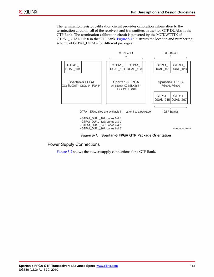
Spartan-6 FPGA GTP Transceivers (Advance Spec) www.xilinx.com 163UG386 (v2.2) April 30, 2010
Pin Description and Design Guidelines
The termination resistor calibration circuit provides calibration information to the termination circuit in all of the receivers and transmitters in the two GTP DUALs in the GTP Bank. The termination calibration circuit is powered by the MGTAVTTTX of GTPA1_DUAL Tile 0 in the GTP Bank. Figure 5-1 illustrates the location and numbering scheme of GTPA1_DUALs for different packages.
Power Supply Connections
Figure 5-2 shows the power supply connections for a GTP Bank.
X-Ref Target - Figure 5-1
Figure 5-1: Spartan-6 FPGA GTP Package Orientation
UG386_c5_11_030410
GTPA1_DUAL_123
GTPA1_DUAL_101
GTPA1_DUAL_267
GTPA1_DUAL_245
Spartan-6 FPGAFG676, FG900
GTP Bank1
GTP Bank2
GTPA1_DUAL_123
GTPA1_DUAL_101
Spartan-6 FPGAAll except XC6SLX25T -
CSG324, FG484
GTP Bank1
GTPA1_DUAL_101
Spartan-6 FPGAXC6SLX25T - CSG324, FG484
GTPA1_DUAL tiles are available in 1, 2, or 4 to a package
- GTPA1_DUAL_101: Lanes 0 & 1- GTPA1_DUAL_123: Lanes 2 & 3- GTPA1_DUAL_245: Lanes 4 & 5- GTPA1_DUAL_267: Lanes 6 & 7
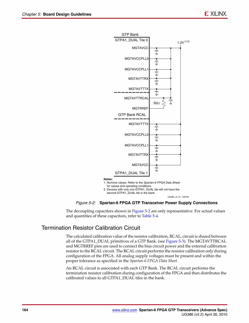
164 www.xilinx.com Spartan-6 FPGA GTP Transceivers (Advance Spec)UG386 (v2.2) April 30, 2010
Chapter 5: Board Design Guidelines
The decoupling capacitors shown in Figure 5-2 are only representative. For actual values and quantities of these capacitors, refer to Table 5-4.
Termination Resistor Calibration CircuitThe calculated calibration value of the resistor calibration, RCAL, circuit is shared between all of the GTPA1_DUAL primitives of a GTP Bank. (see Figure 5-3). The MGTAVTTRCAL and MGTRREF pins are used to connect the bias circuit power and the external calibration resistor to the RCAL circuit. The RCAL circuit performs the resistor calibration only during configuration of the FPGA. All analog supply voltages must be present and within the proper tolerance as specified in the Spartan-6 FPGA Data Sheet.
An RCAL circuit is associated with each GTP Bank. The RCAL circuit performs the termination resistor calibration during configuration of the FPGA and then distributes the calibrated values to all GTPA1_DUAL tiles in the bank.
X-Ref Target - Figure 5-2
Figure 5-2: Spartan-6 FPGA GTP Transceiver Power Supply Connections
MGTAVCC
MGTAVCCPLL0
MGTAVCCPLL1
MGTAVTTRX
MGTAVTTTX
MGTAVTTRCAL
MGTRREF
50Ω
MGTAVCC
UG386_c5_01_100709
MGTAVCCPLL0
MGTAVCCPLL1
MGTAVTTRX
MGTAVTTTX
GTP Bank
GTPA1_DUAL Tile 0
GTPA1_DUAL Tile 1
GTP Bank RCAL
1.2V (1,2)
Notes:1. Nominal values. Refer to the Spartan-6 FPGA Data Sheet for values and operating conditions.2. Devices with only one GTPA1_DUAL tile will not have the second GTPA1_DUAL tile in the bank.
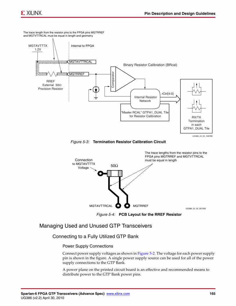
Spartan-6 FPGA GTP Transceivers (Advance Spec) www.xilinx.com 165UG386 (v2.2) April 30, 2010
Pin Description and Design Guidelines
Managing Used and Unused GTP Transceivers
Connecting to a Fully Utilized GTP Bank
Power Supply Connections
Connect power supply voltages as shown in Figure 5-2. The voltage for each power supply pin is shown in the figure. A single power supply source can be used for all of the power supply connections to the GTP Bank.
A power plane on the printed circuit board is an effective and recommended means to distribute power to the GTP Bank power pins.
X-Ref Target - Figure 5-3
Figure 5-3: Termination Resistor Calibration Circuit
MGTAVTTRCAL
MGTRREF
Internal to FPGA
“Master RCAL” GTPA1_DUAL Tile for Resistor Calibration
Internal ResistorNetwork
rCtrl[4:0]
Binary Resistor Calibration (BRcal)
UG386_c5_02_100709
Com
para
tor
The trace length from the resistor pins to the FPGA pins MGTRREF and MGTVTTRCAL must be equal in length and geometry
RREF External 50Ω
Precision Resistor
MGTAVTTTX1.2V
RX/TXTermination
in eachGTPA1_DUAL Tile
X-Ref Target - Figure 5-4
Figure 5-4: PCB Layout for the RREF Resistor
MGTAVTTRCAL MGTRREF
50Ω
Connectionto MGTAVTTTX
Voltage
The trace lengths from the resistor pins to theFPGA pins MGTRREF and MGTVTTRCALmust be equal in length
UG386_c5_03_051509
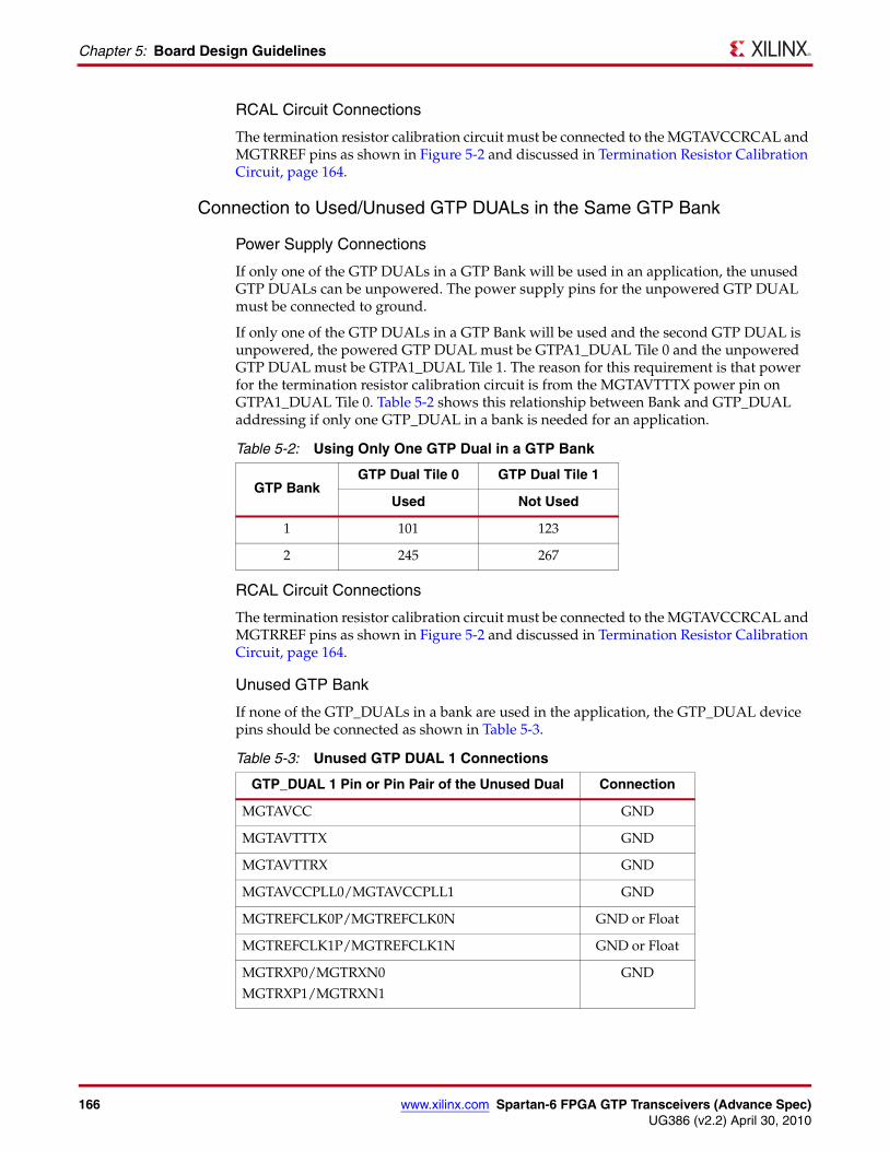
166 www.xilinx.com Spartan-6 FPGA GTP Transceivers (Advance Spec)UG386 (v2.2) April 30, 2010
Chapter 5: Board Design Guidelines
RCAL Circuit Connections
The termination resistor calibration circuit must be connected to the MGTAVCCRCAL and MGTRREF pins as shown in Figure 5-2 and discussed in Termination Resistor Calibration Circuit, page 164.
Connection to Used/Unused GTP DUALs in the Same GTP Bank
Power Supply Connections
If only one of the GTP DUALs in a GTP Bank will be used in an application, the unused GTP DUALs can be unpowered. The power supply pins for the unpowered GTP DUAL must be connected to ground.
If only one of the GTP DUALs in a GTP Bank will be used and the second GTP DUAL is unpowered, the powered GTP DUAL must be GTPA1_DUAL Tile 0 and the unpowered GTP DUAL must be GTPA1_DUAL Tile 1. The reason for this requirement is that power for the termination resistor calibration circuit is from the MGTAVTTTX power pin on GTPA1_DUAL Tile 0. Table 5-2 shows this relationship between Bank and GTP_DUAL addressing if only one GTP_DUAL in a bank is needed for an application.
RCAL Circuit Connections
The termination resistor calibration circuit must be connected to the MGTAVCCRCAL and MGTRREF pins as shown in Figure 5-2 and discussed in Termination Resistor Calibration Circuit, page 164.
Unused GTP Bank
If none of the GTP_DUALs in a bank are used in the application, the GTP_DUAL device pins should be connected as shown in Table 5-3.
Table 5-2: Using Only One GTP Dual in a GTP Bank
GTP BankGTP Dual Tile 0 GTP Dual Tile 1
Used Not Used
1 101 123
2 245 267
Table 5-3: Unused GTP DUAL 1 Connections
GTP_DUAL 1 Pin or Pin Pair of the Unused Dual Connection
MGTAVCC GND
MGTAVTTTX GND
MGTAVTTRX GND
MGTAVCCPLL0/MGTAVCCPLL1 GND
MGTREFCLK0P/MGTREFCLK0N GND or Float
MGTREFCLK1P/MGTREFCLK1N GND or Float
MGTRXP0/MGTRXN0
MGTRXP1/MGTRXN1
GND
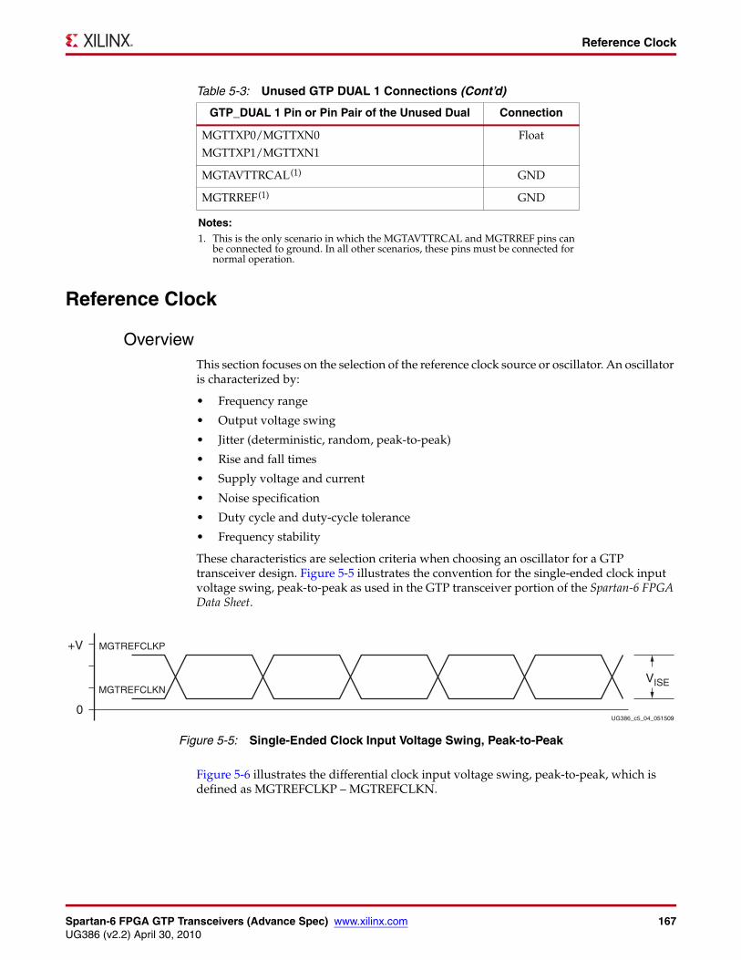
Spartan-6 FPGA GTP Transceivers (Advance Spec) www.xilinx.com 167UG386 (v2.2) April 30, 2010
Reference Clock
Reference Clock
OverviewThis section focuses on the selection of the reference clock source or oscillator. An oscillator is characterized by:
• Frequency range
• Output voltage swing
• Jitter (deterministic, random, peak-to-peak)
• Rise and fall times
• Supply voltage and current
• Noise specification
• Duty cycle and duty-cycle tolerance
• Frequency stability
These characteristics are selection criteria when choosing an oscillator for a GTP transceiver design. Figure 5-5 illustrates the convention for the single-ended clock input voltage swing, peak-to-peak as used in the GTP transceiver portion of the Spartan-6 FPGA Data Sheet.
Figure 5-6 illustrates the differential clock input voltage swing, peak-to-peak, which is defined as MGTREFCLKP – MGTREFCLKN.
MGTTXP0/MGTTXN0
MGTTXP1/MGTTXN1
Float
MGTAVTTRCAL(1) GND
MGTRREF(1) GND
Notes: 1. This is the only scenario in which the MGTAVTTRCAL and MGTRREF pins can
be connected to ground. In all other scenarios, these pins must be connected for normal operation.
Table 5-3: Unused GTP DUAL 1 Connections (Cont’d)
GTP_DUAL 1 Pin or Pin Pair of the Unused Dual Connection
X-Ref Target - Figure 5-5
Figure 5-5: Single-Ended Clock Input Voltage Swing, Peak-to-Peak
0
+V MGTREFCLKP
MGTREFCLKNVISE
UG386_c5_04_051509
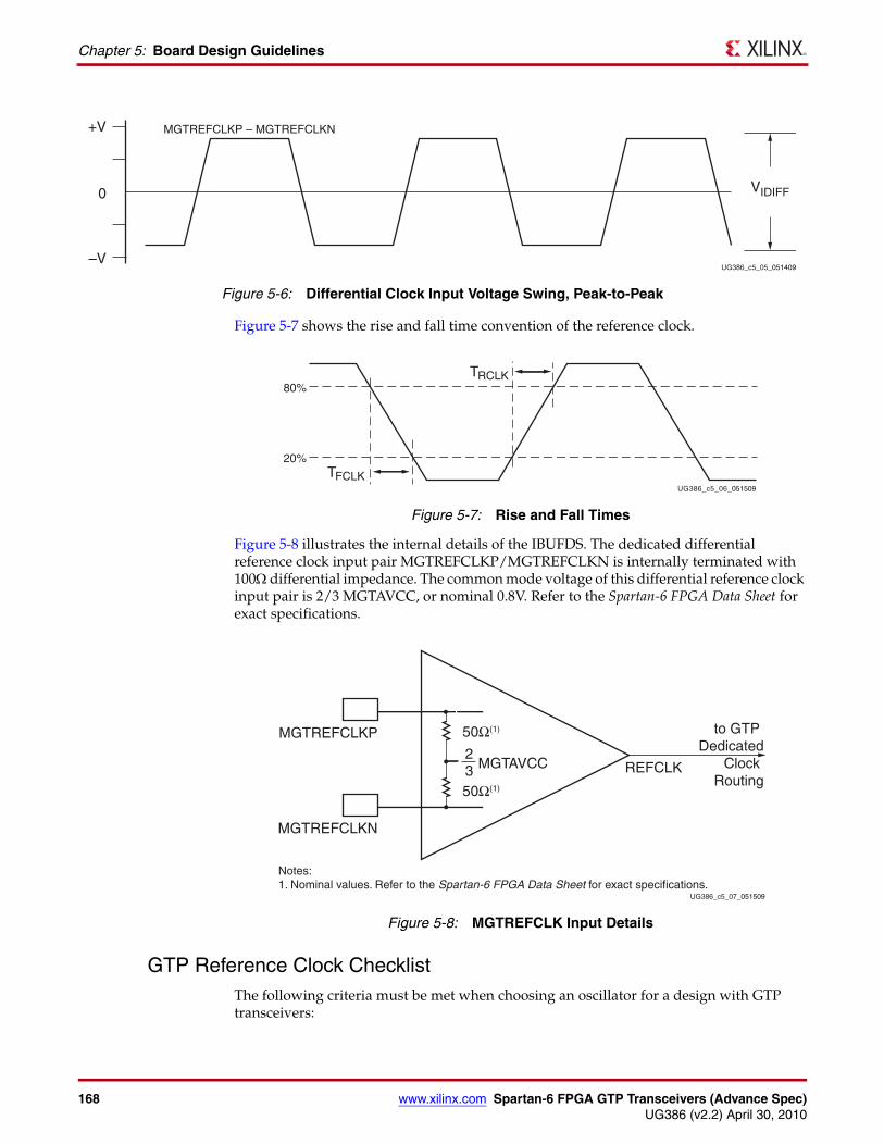
168 www.xilinx.com Spartan-6 FPGA GTP Transceivers (Advance Spec)UG386 (v2.2) April 30, 2010
Chapter 5: Board Design Guidelines
Figure 5-7 shows the rise and fall time convention of the reference clock.
Figure 5-8 illustrates the internal details of the IBUFDS. The dedicated differential reference clock input pair MGTREFCLKP/MGTREFCLKN is internally terminated with 100Ω differential impedance. The common mode voltage of this differential reference clock input pair is 2/3 MGTAVCC, or nominal 0.8V. Refer to the Spartan-6 FPGA Data Sheet for exact specifications.
GTP Reference Clock ChecklistThe following criteria must be met when choosing an oscillator for a design with GTP transceivers:
X-Ref Target - Figure 5-6
Figure 5-6: Differential Clock Input Voltage Swing, Peak-to-Peak
0
+V
–V
MGTREFCLKP – MGTREFCLKN
VIDIFF
UG386_c5_05_051409
X-Ref Target - Figure 5-7
Figure 5-7: Rise and Fall Times
X-Ref Target - Figure 5-8
Figure 5-8: MGTREFCLK Input Details
UG386_c5_06_051509
80%
20%TFCLK
TRCLK
UG386_c5_07_051509
to GTP Dedicated
Clock Routing
REFCLK
MGTREFCLKP
MGTREFCLKN
Notes:1. Nominal values. Refer to the Spartan-6 FPGA Data Sheet for exact specifications.
MGTAVCC23
50Ω(1)
50Ω(1)
Spartan-6 FPGA GTP Transceivers (Advance Spec) www.xilinx.com 169UG386 (v2.2) April 30, 2010
Reference Clock
• Provide AC coupling between the oscillator output pins and the dedicated GTPA1_DUAL clock input pins.
• Ensure that the differential voltage swing of the reference clock is the range as specified in the Spartan-6 FPGA Data Sheet (the nominal range is 200 mV – 2000 mV, and the nominal typical value is 1200 mV).
• Meet or exceed the reference clock characteristics as specified in the Spartan-6 FPGA Data Sheet.
• Meet or exceed the reference clock characteristics as specified in the standard for which the GTP transceiver provides physical layer support.
• Fulfill the oscillator vendor's requirement regarding power supply, board layout, and noise specification.
• Provide a dedicated point-to-point connection between the oscillator and GTPA1_DUAL clock input pins.
• Keep impedance discontinuities on the differential transmission lines to a minimum (impedance discontinuities generate jitter).
• Instantiate any GTPA1_DUAL tile that sources a reference clock.
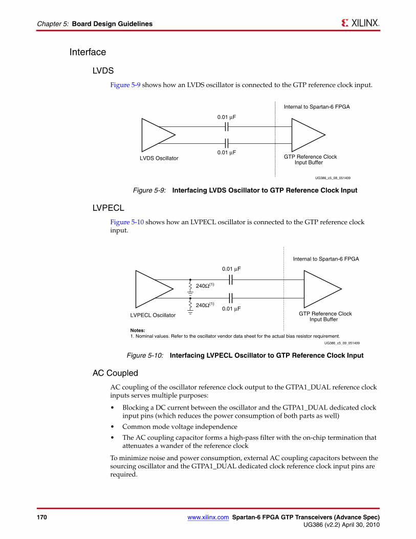
170 www.xilinx.com Spartan-6 FPGA GTP Transceivers (Advance Spec)UG386 (v2.2) April 30, 2010
Chapter 5: Board Design Guidelines
Interface
LVDS
Figure 5-9 shows how an LVDS oscillator is connected to the GTP reference clock input.
LVPECL
Figure 5-10 shows how an LVPECL oscillator is connected to the GTP reference clock input.
AC Coupled
AC coupling of the oscillator reference clock output to the GTPA1_DUAL reference clock inputs serves multiple purposes:
• Blocking a DC current between the oscillator and the GTPA1_DUAL dedicated clock input pins (which reduces the power consumption of both parts as well)
• Common mode voltage independence
• The AC coupling capacitor forms a high-pass filter with the on-chip termination that attenuates a wander of the reference clock
To minimize noise and power consumption, external AC coupling capacitors between the sourcing oscillator and the GTPA1_DUAL dedicated clock reference clock input pins are required.
X-Ref Target - Figure 5-9
Figure 5-9: Interfacing LVDS Oscillator to GTP Reference Clock Input
LVDS Oscillator
0.01 μF
UG386_c5_08_051409
0.01 μFGTP Reference Clock
Input Buffer
Internal to Spartan-6 FPGA
X-Ref Target - Figure 5-10
Figure 5-10: Interfacing LVPECL Oscillator to GTP Reference Clock Input
LVPECL Oscillator
Notes:1. Nominal values. Refer to the oscillator vendor data sheet for the actual bias resistor requirement.
Internal to Spartan-6 FPGA
GTP Reference Clock Input Buffer
0.01 μF
0.01 μF
240Ω(1)
240Ω(1)
UG386_c5_09_051409
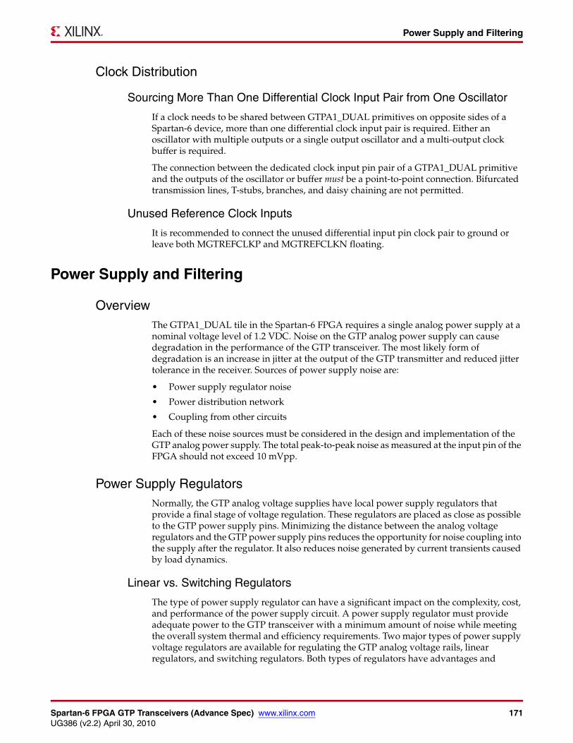
Spartan-6 FPGA GTP Transceivers (Advance Spec) www.xilinx.com 171UG386 (v2.2) April 30, 2010
Power Supply and Filtering
Clock Distribution
Sourcing More Than One Differential Clock Input Pair from One Oscillator
If a clock needs to be shared between GTPA1_DUAL primitives on opposite sides of a Spartan-6 device, more than one differential clock input pair is required. Either an oscillator with multiple outputs or a single output oscillator and a multi-output clock buffer is required.
The connection between the dedicated clock input pin pair of a GTPA1_DUAL primitive and the outputs of the oscillator or buffer must be a point-to-point connection. Bifurcated transmission lines, T-stubs, branches, and daisy chaining are not permitted.
Unused Reference Clock Inputs
It is recommended to connect the unused differential input pin clock pair to ground or leave both MGTREFCLKP and MGTREFCLKN floating.
Power Supply and Filtering
OverviewThe GTPA1_DUAL tile in the Spartan-6 FPGA requires a single analog power supply at a nominal voltage level of 1.2 VDC. Noise on the GTP analog power supply can cause degradation in the performance of the GTP transceiver. The most likely form of degradation is an increase in jitter at the output of the GTP transmitter and reduced jitter tolerance in the receiver. Sources of power supply noise are:
• Power supply regulator noise
• Power distribution network
• Coupling from other circuits
Each of these noise sources must be considered in the design and implementation of the GTP analog power supply. The total peak-to-peak noise as measured at the input pin of the FPGA should not exceed 10 mVpp.
Power Supply RegulatorsNormally, the GTP analog voltage supplies have local power supply regulators that provide a final stage of voltage regulation. These regulators are placed as close as possible to the GTP power supply pins. Minimizing the distance between the analog voltage regulators and the GTP power supply pins reduces the opportunity for noise coupling into the supply after the regulator. It also reduces noise generated by current transients caused by load dynamics.
Linear vs. Switching Regulators
The type of power supply regulator can have a significant impact on the complexity, cost, and performance of the power supply circuit. A power supply regulator must provide adequate power to the GTP transceiver with a minimum amount of noise while meeting the overall system thermal and efficiency requirements. Two major types of power supply voltage regulators are available for regulating the GTP analog voltage rails, linear regulators, and switching regulators. Both types of regulators have advantages and
172 www.xilinx.com Spartan-6 FPGA GTP Transceivers (Advance Spec)UG386 (v2.2) April 30, 2010
Chapter 5: Board Design Guidelines
disadvantages. The optimal choice of regulator type depends on system requirements such as:
• Physical size
• Thermal budget
• Power efficiency
• Cost
Linear Regulator
A linear regulator is usually the simplest means to provide voltage regulation for the GTP analog supply rails. Inherently, a linear regulator does not inject significant noise into the regulated output voltage. Some linear regulators provide noise rejection at the output from noise present on the voltage input. Another advantage of the linear regulator is that it usually requires a minimal number of external components to realize a circuit on the printed circuit board.
There are potentially two major disadvantages to linear regulators: minimum dropout voltage and limited efficiency. Linear regulators require an input voltage that is higher than the output voltage. This minimum dropout voltage often is dependent on the load current. Even low dropout linear regulators require a minimum difference between the input voltage and the output voltage of the regulator. The system power supply design must consider the minimum dropout voltage requirements of the linear regulators.
The efficiency of a linear regulator is dependent on voltage difference between the input and output of the linear regulator. For instance, if the input voltage of the regulator is 2.5 VDC and the output voltage of the regulator is 1.2 VDC, the voltage difference is 1.3 VDC. Assuming that the current into the regulator is essentially equal to the current out of the regulator, the maximum efficiency of the regulator is 48%. This means that for every watt delivered to the load, the system must consume an additional watt for regulation. This power consumed by the regulator generates heat that must be dissipated by the system. Providing a means to dissipate the heat generated by the linear regulator can drive up the system cost. So, even though the linear regulator appears to have an advantage over the switching regulator from a simple component count and complexity cost perspective, if the overall system cost is considered, including power consumption and heat dissipation, the linear regulator can actually be at a disadvantage in high-current applications.
Switching Regulator
A switching regulator can provide a very efficient means to deliver a well-regulated voltage for the GTP analog power supply. Unlike the linear regulator, the switching regulator does not depend on the voltage drop between the input voltage of the regulator and the output voltage to provide regulation. Therefore, the switching regulator can supply large amounts of current to the load while maintaining high power efficiency. It is not uncommon for a switching regulator to maintain efficiencies of 95% or greater. This efficiency is not severely impacted by the voltage drop between the input of the regulator and the output, and it is impacted by the load current to a much lesser degree than the linear regulator. Because of the efficiency of the switching regulator, the system does not need to supply as much power to the circuit, and it does not need to provide a means to dissipate power consumed by the regulator.
The disadvantages of the switching regulator are complexity of the circuit and noise generated by the regulator switching function. Switching regulator circuits are usually more complex than linear regulator circuits. This shortcoming in switching regulators has been addressed by several switching regulator component vendors. Normally, a switching power supply regulation circuit requires a switching transistor element, an inductor, and a
Spartan-6 FPGA GTP Transceivers (Advance Spec) www.xilinx.com 173UG386 (v2.2) April 30, 2010
Power Supply and Filtering
capacitor. Depending on the required efficiency and load requirements, a switching regulator circuit might require external switching transistors and inductors. Besides the component count, these switching regulators require very careful placement and routing on the printed circuit board to be effective.
Switching regulators generate significant noise and, therefore, usually require additional filtering before the voltage is delivered to the GTP analog power supply input of the Spartan-6 FPGA. As mentioned in Overview, page 171, the amplitude of the noise should be limited to less than 10 mVpp. Therefore, the power supply filter should be designed to attenuate the noise from the switching regulator so that it meets this requirement.
Power Supply Distribution Network
Power Supply Decoupling Capacitors
For the analog power supplies of the Spartan-6 FPGA GTP transceiver, the decoupling capacitors lower the impedance between the power plane and ground. With minimal impedance to ground, the power plane can provide a means to locally attenuate noise. The advantage of this is isolation between the GTP transceivers and external circuits as well as between transceivers within the same package.
The primary purpose of decoupling capacitors in the GTP transceiver analog power supplies is to reduce the amplitude of noise from the power supply source and other circuits on the printed circuit board. The suggested filtering for the power supplies, MGTAVCC and MGTAVTTTX, MGTAVTTRX and MGTAVCCPLL, is shown in Table 5-4.
Printed Circuit Board DesignOptimal performance of the Spartan-6 FPGA GTP transceivers requires careful consideration in the design of the printed circuit board. The areas of printed circuit board design that must be considered are the board stackup, component placement, and signal routing. The printed circuit board design includes these components:
• Power distribution network for 1.2 VDC MGT Analog Power Supply
• Data lines for the receiver and transmitter
• Reference clock connections between the source oscillator and the GTP reference clock input
Table 5-4: Recommended Minimum Decoupling for Spartan-6 FPGA GTPA1_DUAL Tiles
Capacitance (µF)
Type Size
Number of Power Plane Decoupling Capacitors
Manufacturer P/NFor 1
GTPA1_DUAL
For 2 GTPA1_DUALs
(1 Bank)
0.22 Ceramic 402 6 8 AVX 04026D224KAT2A
Kemet C0402C224K9PAC
Murata GRM155R60J224KE01D
4.7 Ceramic 0603 1 2 AVX 06036D475KAT2A
Kemet C0603C475K9PAC
Murata GRM188R60J475KE19D
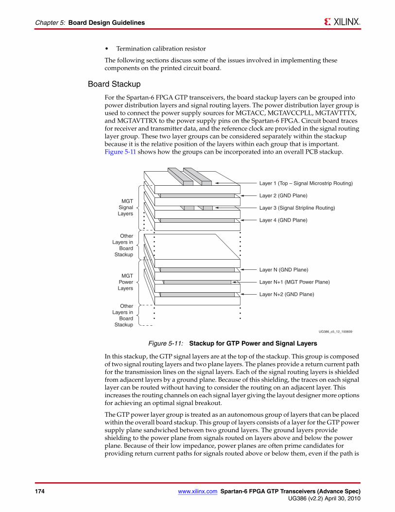
174 www.xilinx.com Spartan-6 FPGA GTP Transceivers (Advance Spec)UG386 (v2.2) April 30, 2010
Chapter 5: Board Design Guidelines
• Termination calibration resistor
The following sections discuss some of the issues involved in implementing these components on the printed circuit board.
Board Stackup
For the Spartan-6 FPGA GTP transceivers, the board stackup layers can be grouped into power distribution layers and signal routing layers. The power distribution layer group is used to connect the power supply sources for MGTACC, MGTAVCCPLL, MGTAVTTTX, and MGTAVTTRX to the power supply pins on the Spartan-6 FPGA. Circuit board traces for receiver and transmitter data, and the reference clock are provided in the signal routing layer group. These two layer groups can be considered separately within the stackup because it is the relative position of the layers within each group that is important. Figure 5-11 shows how the groups can be incorporated into an overall PCB stackup.
In this stackup, the GTP signal layers are at the top of the stackup. This group is composed of two signal routing layers and two plane layers. The planes provide a return current path for the transmission lines on the signal layers. Each of the signal routing layers is shielded from adjacent layers by a ground plane. Because of this shielding, the traces on each signal layer can be routed without having to consider the routing on an adjacent layer. This increases the routing channels on each signal layer giving the layout designer more options for achieving an optimal signal breakout.
The GTP power layer group is treated as an autonomous group of layers that can be placed within the overall board stackup. This group of layers consists of a layer for the GTP power supply plane sandwiched between two ground layers. The ground layers provide shielding to the power plane from signals routed on layers above and below the power plane. Because of their low impedance, power planes are often prime candidates for providing return current paths for signals routed above or below them, even if the path is
X-Ref Target - Figure 5-11
Figure 5-11: Stackup for GTP Power and Signal Layers
UG386_c5_12_100609
MGTSignalLayers
Layer 1 (Top – Signal Microstrip Routing)
Layer 2 (GND Plane)
Layer 3 (Signal Stripline Routing)
Layer 4 (GND Plane)
Layer N (GND Plane)
Layer N+1 (MGT Power Plane)
Layer N+2 (GND Plane)
MGTPowerLayers
OtherLayers in
BoardStackup
OtherLayers in
BoardStackup
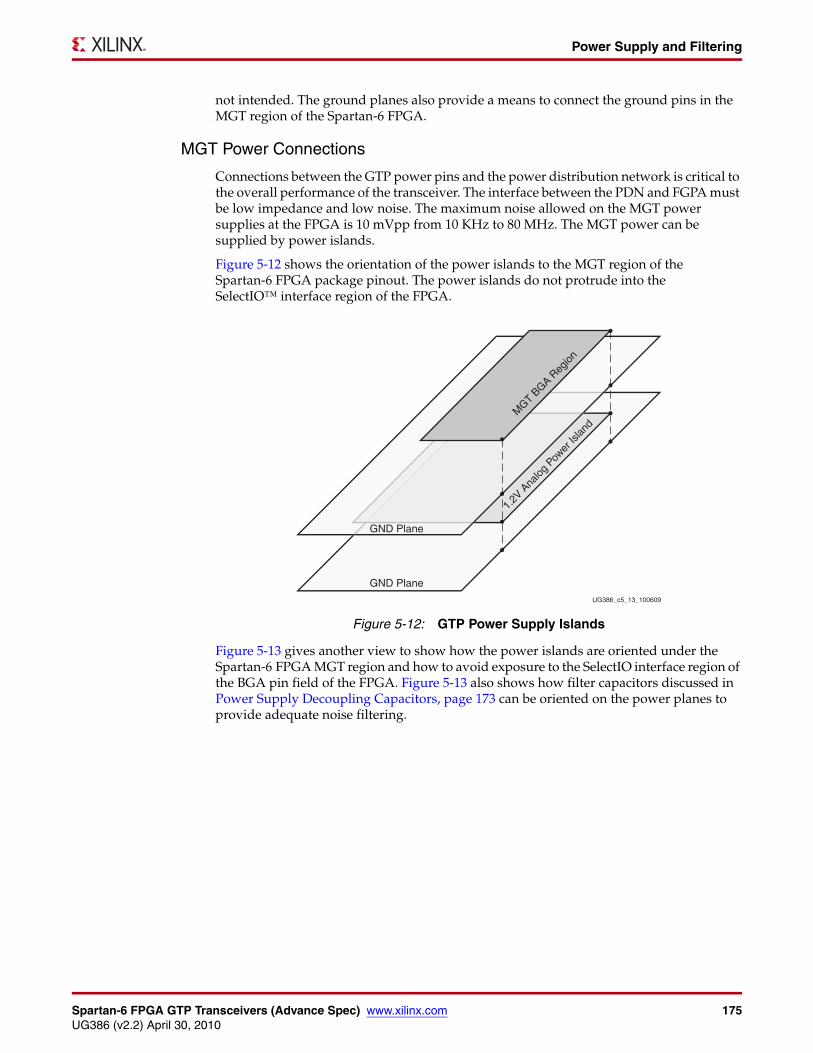
Spartan-6 FPGA GTP Transceivers (Advance Spec) www.xilinx.com 175UG386 (v2.2) April 30, 2010
Power Supply and Filtering
not intended. The ground planes also provide a means to connect the ground pins in the MGT region of the Spartan-6 FPGA.
MGT Power Connections
Connections between the GTP power pins and the power distribution network is critical to the overall performance of the transceiver. The interface between the PDN and FGPA must be low impedance and low noise. The maximum noise allowed on the MGT power supplies at the FPGA is 10 mVpp from 10 KHz to 80 MHz. The MGT power can be supplied by power islands.
Figure 5-12 shows the orientation of the power islands to the MGT region of the Spartan-6 FPGA package pinout. The power islands do not protrude into the SelectIO™ interface region of the FPGA.
Figure 5-13 gives another view to show how the power islands are oriented under the Spartan-6 FPGA MGT region and how to avoid exposure to the SelectIO interface region of the BGA pin field of the FPGA. Figure 5-13 also shows how filter capacitors discussed in Power Supply Decoupling Capacitors, page 173 can be oriented on the power planes to provide adequate noise filtering.
X-Ref Target - Figure 5-12
Figure 5-12: GTP Power Supply Islands
UG386_c5_13_100609
MGT B
GA Reg
ion
1.2V
Ana
log P
ower
Islan
d
GND Plane
GND Plane
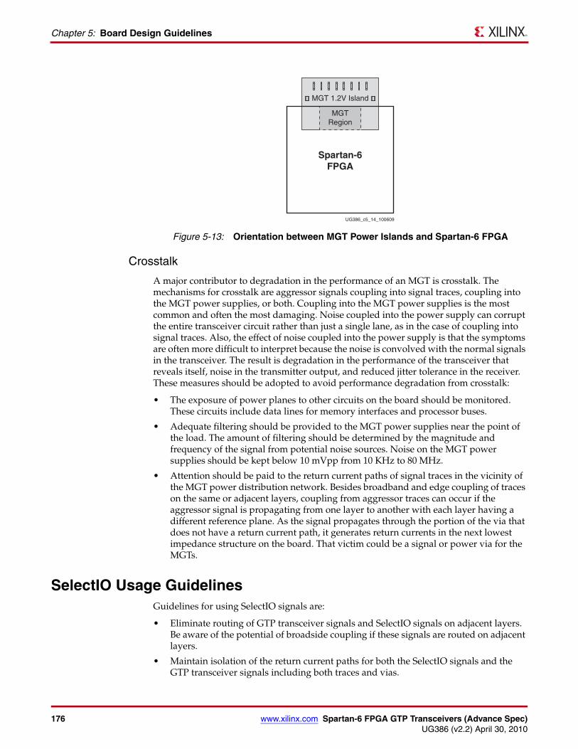
176 www.xilinx.com Spartan-6 FPGA GTP Transceivers (Advance Spec)UG386 (v2.2) April 30, 2010
Chapter 5: Board Design Guidelines
Crosstalk
A major contributor to degradation in the performance of an MGT is crosstalk. The mechanisms for crosstalk are aggressor signals coupling into signal traces, coupling into the MGT power supplies, or both. Coupling into the MGT power supplies is the most common and often the most damaging. Noise coupled into the power supply can corrupt the entire transceiver circuit rather than just a single lane, as in the case of coupling into signal traces. Also, the effect of noise coupled into the power supply is that the symptoms are often more difficult to interpret because the noise is convolved with the normal signals in the transceiver. The result is degradation in the performance of the transceiver that reveals itself, noise in the transmitter output, and reduced jitter tolerance in the receiver. These measures should be adopted to avoid performance degradation from crosstalk:
• The exposure of power planes to other circuits on the board should be monitored. These circuits include data lines for memory interfaces and processor buses.
• Adequate filtering should be provided to the MGT power supplies near the point of the load. The amount of filtering should be determined by the magnitude and frequency of the signal from potential noise sources. Noise on the MGT power supplies should be kept below 10 mVpp from 10 KHz to 80 MHz.
• Attention should be paid to the return current paths of signal traces in the vicinity of the MGT power distribution network. Besides broadband and edge coupling of traces on the same or adjacent layers, coupling from aggressor traces can occur if the aggressor signal is propagating from one layer to another with each layer having a different reference plane. As the signal propagates through the portion of the via that does not have a return current path, it generates return currents in the next lowest impedance structure on the board. That victim could be a signal or power via for the MGTs.
SelectIO Usage GuidelinesGuidelines for using SelectIO signals are:
• Eliminate routing of GTP transceiver signals and SelectIO signals on adjacent layers. Be aware of the potential of broadside coupling if these signals are routed on adjacent layers.
• Maintain isolation of the return current paths for both the SelectIO signals and the GTP transceiver signals including both traces and vias.
X-Ref Target - Figure 5-13
Figure 5-13: Orientation between MGT Power Islands and Spartan-6 FPGA
UG386_c5_14_100609
Spartan-6FPGA
MGTRegion
MGT 1.2V Island
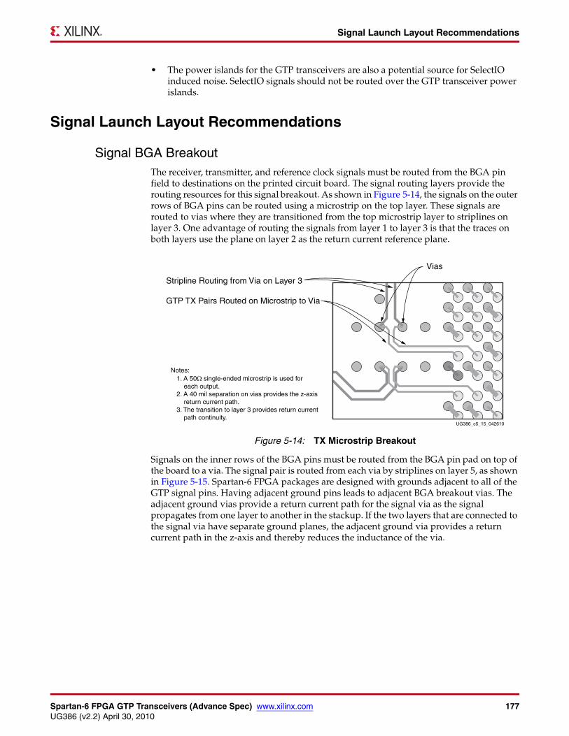
Spartan-6 FPGA GTP Transceivers (Advance Spec) www.xilinx.com 177UG386 (v2.2) April 30, 2010
Signal Launch Layout Recommendations
• The power islands for the GTP transceivers are also a potential source for SelectIO induced noise. SelectIO signals should not be routed over the GTP transceiver power islands.
Signal Launch Layout Recommendations
Signal BGA BreakoutThe receiver, transmitter, and reference clock signals must be routed from the BGA pin field to destinations on the printed circuit board. The signal routing layers provide the routing resources for this signal breakout. As shown in Figure 5-14, the signals on the outer rows of BGA pins can be routed using a microstrip on the top layer. These signals are routed to vias where they are transitioned from the top microstrip layer to striplines on layer 3. One advantage of routing the signals from layer 1 to layer 3 is that the traces on both layers use the plane on layer 2 as the return current reference plane.
Signals on the inner rows of the BGA pins must be routed from the BGA pin pad on top of the board to a via. The signal pair is routed from each via by striplines on layer 5, as shown in Figure 5-15. Spartan-6 FPGA packages are designed with grounds adjacent to all of the GTP signal pins. Having adjacent ground pins leads to adjacent BGA breakout vias. The adjacent ground vias provide a return current path for the signal via as the signal propagates from one layer to another in the stackup. If the two layers that are connected to the signal via have separate ground planes, the adjacent ground via provides a return current path in the z-axis and thereby reduces the inductance of the via.
X-Ref Target - Figure 5-14
Figure 5-14: TX Microstrip Breakout
Stripline Routing from Via on Layer 3
GTP TX Pairs Routed on Microstrip to Via
Vias
UG386_c5_15_042610
Notes: 1. A 50Ω single-ended microstrip is used for each output.2. A 40 mil separation on vias provides the z-axis return current path.3. The transition to layer 3 provides return current path continuity.
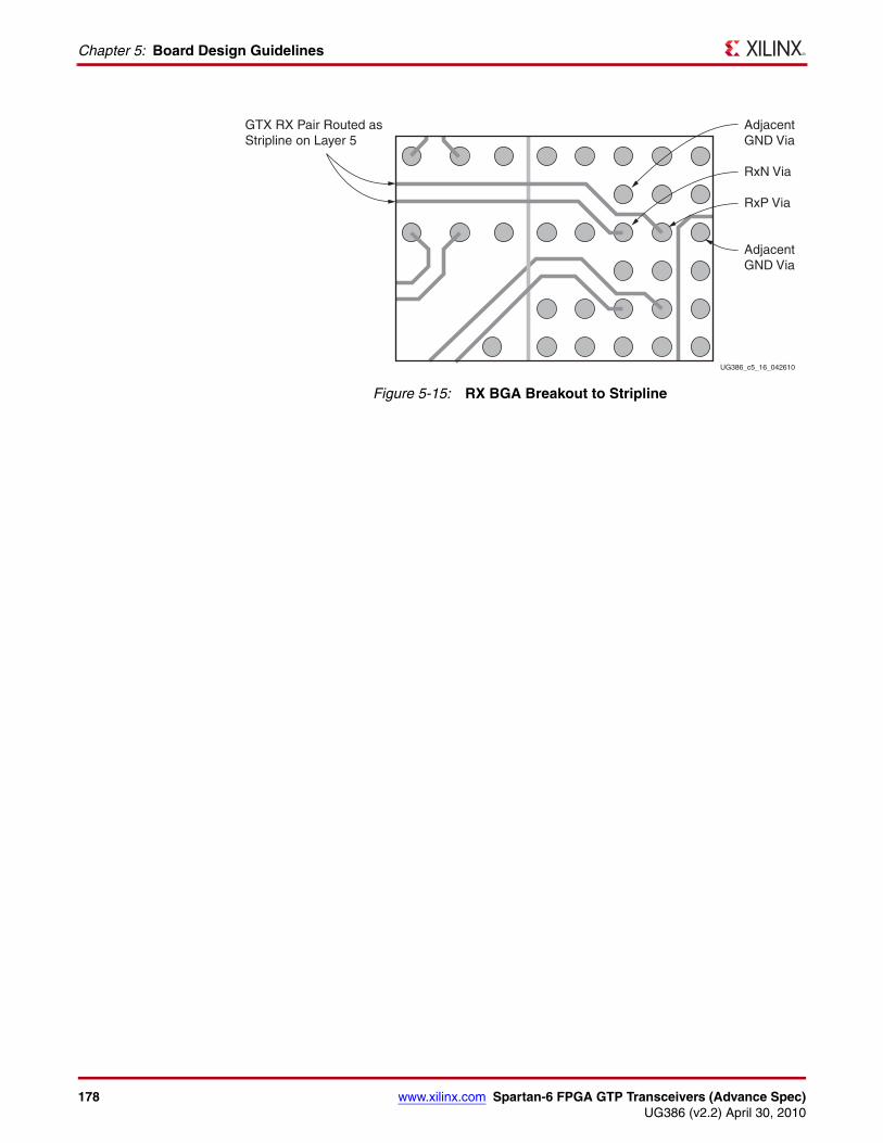
178 www.xilinx.com Spartan-6 FPGA GTP Transceivers (Advance Spec)UG386 (v2.2) April 30, 2010
Chapter 5: Board Design Guidelines
X-Ref Target - Figure 5-15
Figure 5-15: RX BGA Breakout to Stripline
GTX RX Pair Routed asStripline on Layer 5
UG386_c5_16_042610
AdjacentGND Via
RxN Via
RxP Via
AdjacentGND Via
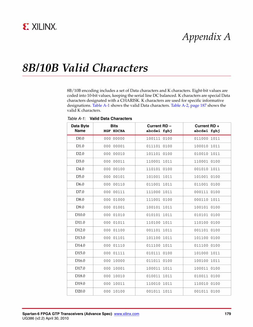
Spartan-6 FPGA GTP Transceivers (Advance Spec) www.xilinx.com 179UG386 (v2.2) April 30, 2010
Appendix A
8B/10B Valid Characters
8B/10B encoding includes a set of Data characters and K characters. Eight-bit values are coded into 10-bit values, keeping the serial line DC balanced. K characters are special Data characters designated with a CHARISK. K characters are used for specific informative designations. Table A-1 shows the valid Data characters. Table A-2, page 187 shows the valid K characters.
Table A-1: Valid Data Characters
Data Byte Name
Bits HGF EDCBA
Current RD –abcdei fghj
Current RD + abcdei fghj
D0.0 000 00000 100111 0100 011000 1011
D1.0 000 00001 011101 0100 100010 1011
D2.0 000 00010 101101 0100 010010 1011
D3.0 000 00011 110001 1011 110001 0100
D4.0 000 00100 110101 0100 001010 1011
D5.0 000 00101 101001 1011 101001 0100
D6.0 000 00110 011001 1011 011001 0100
D7.0 000 00111 111000 1011 000111 0100
D8.0 000 01000 111001 0100 000110 1011
D9.0 000 01001 100101 1011 100101 0100
D10.0 000 01010 010101 1011 010101 0100
D11.0 000 01011 110100 1011 110100 0100
D12.0 000 01100 001101 1011 001101 0100
D13.0 000 01101 101100 1011 101100 0100
D14.0 000 01110 011100 1011 011100 0100
D15.0 000 01111 010111 0100 101000 1011
D16.0 000 10000 011011 0100 100100 1011
D17.0 000 10001 100011 1011 100011 0100
D18.0 000 10010 010011 1011 010011 0100
D19.0 000 10011 110010 1011 110010 0100
D20.0 000 10100 001011 1011 001011 0100
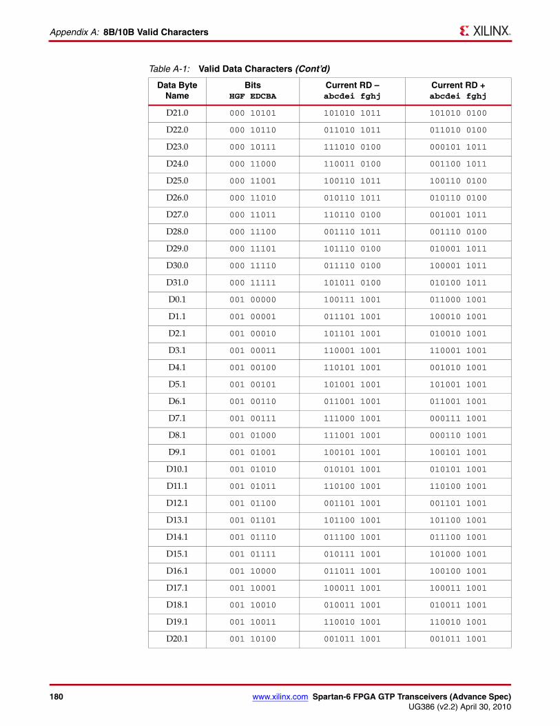
180 www.xilinx.com Spartan-6 FPGA GTP Transceivers (Advance Spec)UG386 (v2.2) April 30, 2010
Appendix A: 8B/10B Valid Characters
D21.0 000 10101 101010 1011 101010 0100
D22.0 000 10110 011010 1011 011010 0100
D23.0 000 10111 111010 0100 000101 1011
D24.0 000 11000 110011 0100 001100 1011
D25.0 000 11001 100110 1011 100110 0100
D26.0 000 11010 010110 1011 010110 0100
D27.0 000 11011 110110 0100 001001 1011
D28.0 000 11100 001110 1011 001110 0100
D29.0 000 11101 101110 0100 010001 1011
D30.0 000 11110 011110 0100 100001 1011
D31.0 000 11111 101011 0100 010100 1011
D0.1 001 00000 100111 1001 011000 1001
D1.1 001 00001 011101 1001 100010 1001
D2.1 001 00010 101101 1001 010010 1001
D3.1 001 00011 110001 1001 110001 1001
D4.1 001 00100 110101 1001 001010 1001
D5.1 001 00101 101001 1001 101001 1001
D6.1 001 00110 011001 1001 011001 1001
D7.1 001 00111 111000 1001 000111 1001
D8.1 001 01000 111001 1001 000110 1001
D9.1 001 01001 100101 1001 100101 1001
D10.1 001 01010 010101 1001 010101 1001
D11.1 001 01011 110100 1001 110100 1001
D12.1 001 01100 001101 1001 001101 1001
D13.1 001 01101 101100 1001 101100 1001
D14.1 001 01110 011100 1001 011100 1001
D15.1 001 01111 010111 1001 101000 1001
D16.1 001 10000 011011 1001 100100 1001
D17.1 001 10001 100011 1001 100011 1001
D18.1 001 10010 010011 1001 010011 1001
D19.1 001 10011 110010 1001 110010 1001
D20.1 001 10100 001011 1001 001011 1001
Table A-1: Valid Data Characters (Cont’d)
Data Byte Name
Bits HGF EDCBA
Current RD –abcdei fghj
Current RD + abcdei fghj

Spartan-6 FPGA GTP Transceivers (Advance Spec) www.xilinx.com 181UG386 (v2.2) April 30, 2010
D21.1 001 10101 101010 1001 101010 1001
D22.1 001 10110 011010 1001 011010 1001
D23.1 001 10111 111010 1001 000101 1001
D24.1 001 11000 110011 1001 001100 1001
D25.1 001 11001 100110 1001 100110 1001
D26.1 001 11010 010110 1001 010110 1001
D27.1 001 11011 110110 1001 001001 1001
D28.1 001 11100 001110 1001 001110 1001
D29.1 001 11101 101110 1001 010001 1001
D30.1 001 11110 011110 1001 100001 1001
D31.1 001 11111 101011 1001 010100 1001
D0.2 010 00000 100111 0101 011000 0101
D1.2 010 00001 011101 0101 100010 0101
D2.2 010 00010 101101 0101 010010 0101
D3.2 010 00011 110001 0101 110001 0101
D4.2 010 00100 110101 0101 001010 0101
D5.2 010 00101 101001 0101 101001 0101
D6.2 010 00110 011001 0101 011001 0101
D7.2 010 00111 111000 0101 000111 0101
D8.2 010 01000 111001 0101 000110 0101
D9.2 010 01001 100101 0101 100101 0101
D10.2 010 01010 010101 0101 010101 0101
D11.2 010 01011 110100 0101 110100 0101
D12.2 010 01100 001101 0101 001101 0101
D13.2 010 01101 101100 0101 101100 0101
D14.2 010 01110 011100 0101 011100 0101
D15.2 010 01111 010111 0101 101000 0101
D16.2 010 10000 011011 0101 100100 0101
D17.2 010 10001 100011 0101 100011 0101
D18.2 010 10010 010011 0101 010011 0101
D19.2 010 10011 110010 0101 110010 0101
D20.2 010 10100 001011 0101 001011 0101
Table A-1: Valid Data Characters (Cont’d)
Data Byte Name
Bits HGF EDCBA
Current RD –abcdei fghj
Current RD + abcdei fghj

182 www.xilinx.com Spartan-6 FPGA GTP Transceivers (Advance Spec)UG386 (v2.2) April 30, 2010
Appendix A: 8B/10B Valid Characters
D21.2 010 10101 101010 0101 101010 0101
D22.2 010 10110 011010 0101 011010 0101
D23.2 010 10111 111010 0101 000101 0101
D24.2 010 11000 110011 0101 001100 0101
D25.2 010 11001 100110 0101 100110 0101
D26.2 010 11010 010110 0101 010110 0101
D27.2 010 11011 110110 0101 001001 0101
D28.2 010 11100 001110 0101 001110 0101
D29.2 010 11101 101110 0101 010001 0101
D30.2 010 11110 011110 0101 100001 0101
D31.2 010 11111 101011 0101 010100 0101
D0.3 011 00000 100111 0011 011000 1100
D1.3 011 00001 011101 0011 100010 1100
D2.3 011 00010 101101 0011 010010 1100
D3.3 011 00011 110001 1100 110001 0011
D4.3 011 00100 110101 0011 001010 1100
D5.3 011 00101 101001 1100 101001 0011
D6.3 011 00110 011001 1100 011001 0011
D7.3 011 00111 111000 1100 000111 0011
D8.3 011 01000 111001 0011 000110 1100
D9.3 011 01001 100101 1100 100101 0011
D10.3 011 01010 010101 1100 010101 0011
D11.3 011 01011 110100 1100 110100 0011
D12.3 011 01100 001101 1100 001101 0011
D13.3 011 01101 101100 1100 101100 0011
D14.3 011 01110 011100 1100 011100 0011
D15.3 011 01111 010111 0011 101000 1100
D16.3 011 10000 011011 0011 100100 1100
D17.3 011 10001 100011 1100 100011 0011
D18.3 011 10010 010011 1100 010011 0011
D19.3 011 10011 110010 1100 110010 0011
D20.3 011 10100 001011 1100 001011 0011
Table A-1: Valid Data Characters (Cont’d)
Data Byte Name
Bits HGF EDCBA
Current RD –abcdei fghj
Current RD + abcdei fghj

Spartan-6 FPGA GTP Transceivers (Advance Spec) www.xilinx.com 183UG386 (v2.2) April 30, 2010
D21.3 011 10101 101010 1100 101010 0011
D22.3 011 10110 011010 1100 011010 0011
D23.3 011 10111 111010 0011 000101 1100
D24.3 011 11000 110011 0011 001100 1100
D25.3 011 11001 100110 1100 100110 0011
D26.3 011 11010 010110 1100 010110 0011
D27.3 011 11011 110110 0011 001001 1100
D28.3 011 11100 001110 1100 001110 0011
D29.3 011 11101 101110 0011 010001 1100
D30.3 011 11110 011110 0011 100001 1100
D31.3 011 11111 101011 0011 010100 1100
D0.4 100 00000 100111 0010 011000 1101
D1.4 100 00001 011101 0010 100010 1101
D2.4 100 00010 101101 0010 010010 1101
D3.4 100 00011 110001 1101 110001 0010
D4.4 100 00100 110101 0010 001010 1101
D5.4 100 00101 101001 1101 101001 0010
D6.4 100 00110 011001 1101 011001 0010
D7.4 100 00111 111000 1101 000111 0010
D8.4 100 01000 111001 0010 000110 1101
D9.4 100 01001 100101 1101 100101 0010
D10.4 100 01010 010101 1101 010101 0010
D11.4 100 01011 110100 1101 110100 0010
D12.4 100 01100 001101 1101 001101 0010
D13.4 100 01101 101100 1101 101100 0010
D14.4 100 01110 011100 1101 011100 0010
D15.4 100 01111 010111 0010 101000 1101
D16.4 100 10000 011011 0010 100100 1101
D17.4 100 10001 100011 1101 100011 0010
D18.4 100 10010 010011 1101 010011 0010
D19.4 100 10011 110010 1101 110010 0010
D20.4 100 10100 001011 1101 001011 0010
Table A-1: Valid Data Characters (Cont’d)
Data Byte Name
Bits HGF EDCBA
Current RD –abcdei fghj
Current RD + abcdei fghj

184 www.xilinx.com Spartan-6 FPGA GTP Transceivers (Advance Spec)UG386 (v2.2) April 30, 2010
Appendix A: 8B/10B Valid Characters
D21.4 100 10101 101010 1101 101010 0010
D22.4 100 10110 011010 1101 011010 0010
D23.4 100 10111 111010 0010 000101 1101
D24.4 100 11000 110011 0010 001100 1101
D25.4 100 11001 100110 1101 100110 0010
D26.4 100 11010 010110 1101 010110 0010
D27.4 100 11011 110110 0010 001001 1101
D28.4 100 11100 001110 1101 001110 0010
D29.4 100 11101 101110 0010 010001 1101
D30.4 100 11110 011110 0010 100001 1101
D31.4 100 11111 101011 0010 010100 1101
D0.5 101 00000 100111 1010 011000 1010
D1.5 101 00001 011101 1010 100010 1010
D2.5 101 00010 101101 1010 010010 1010
D3.5 101 00011 110001 1010 110001 1010
D4.5 101 00100 110101 1010 001010 1010
D5.5 101 00101 101001 1010 101001 1010
D6.5 101 00110 011001 1010 011001 1010
D7.5 101 00111 111000 1010 000111 1010
D8.5 101 01000 111001 1010 000110 1010
D9.5 101 01001 100101 1010 100101 1010
D10.5 101 01010 010101 1010 010101 1010
D11.5 101 01011 110100 1010 110100 1010
D12.5 101 01100 001101 1010 001101 1010
D13.5 101 01101 101100 1010 101100 1010
D14.5 101 01110 011100 1010 011100 1010
D15.5 101 01111 010111 1010 101000 1010
D16.5 101 10000 011011 1010 100100 1010
D17.5 101 10001 100011 1010 100011 1010
D18.5 101 10010 010011 1010 010011 1010
D19.5 101 10011 110010 1010 110010 1010
D20.5 101 10100 001011 1010 001011 1010
Table A-1: Valid Data Characters (Cont’d)
Data Byte Name
Bits HGF EDCBA
Current RD –abcdei fghj
Current RD + abcdei fghj
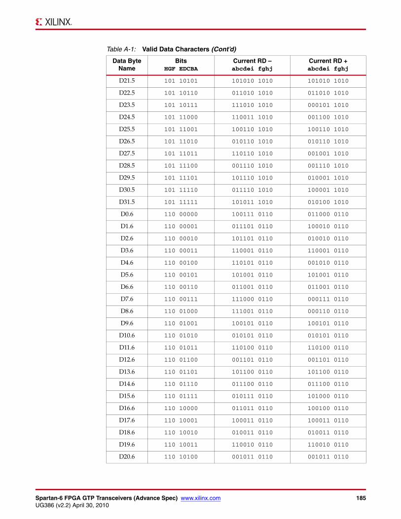
Spartan-6 FPGA GTP Transceivers (Advance Spec) www.xilinx.com 185UG386 (v2.2) April 30, 2010
D21.5 101 10101 101010 1010 101010 1010
D22.5 101 10110 011010 1010 011010 1010
D23.5 101 10111 111010 1010 000101 1010
D24.5 101 11000 110011 1010 001100 1010
D25.5 101 11001 100110 1010 100110 1010
D26.5 101 11010 010110 1010 010110 1010
D27.5 101 11011 110110 1010 001001 1010
D28.5 101 11100 001110 1010 001110 1010
D29.5 101 11101 101110 1010 010001 1010
D30.5 101 11110 011110 1010 100001 1010
D31.5 101 11111 101011 1010 010100 1010
D0.6 110 00000 100111 0110 011000 0110
D1.6 110 00001 011101 0110 100010 0110
D2.6 110 00010 101101 0110 010010 0110
D3.6 110 00011 110001 0110 110001 0110
D4.6 110 00100 110101 0110 001010 0110
D5.6 110 00101 101001 0110 101001 0110
D6.6 110 00110 011001 0110 011001 0110
D7.6 110 00111 111000 0110 000111 0110
D8.6 110 01000 111001 0110 000110 0110
D9.6 110 01001 100101 0110 100101 0110
D10.6 110 01010 010101 0110 010101 0110
D11.6 110 01011 110100 0110 110100 0110
D12.6 110 01100 001101 0110 001101 0110
D13.6 110 01101 101100 0110 101100 0110
D14.6 110 01110 011100 0110 011100 0110
D15.6 110 01111 010111 0110 101000 0110
D16.6 110 10000 011011 0110 100100 0110
D17.6 110 10001 100011 0110 100011 0110
D18.6 110 10010 010011 0110 010011 0110
D19.6 110 10011 110010 0110 110010 0110
D20.6 110 10100 001011 0110 001011 0110
Table A-1: Valid Data Characters (Cont’d)
Data Byte Name
Bits HGF EDCBA
Current RD –abcdei fghj
Current RD + abcdei fghj
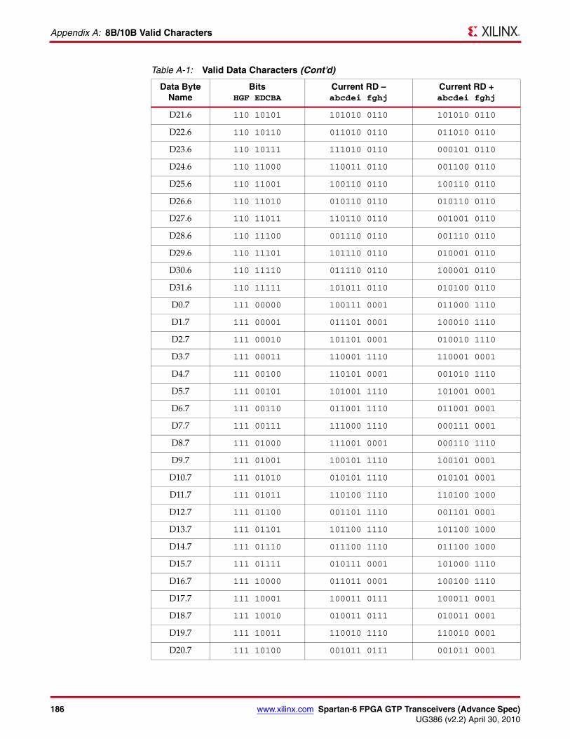
186 www.xilinx.com Spartan-6 FPGA GTP Transceivers (Advance Spec)UG386 (v2.2) April 30, 2010
Appendix A: 8B/10B Valid Characters
D21.6 110 10101 101010 0110 101010 0110
D22.6 110 10110 011010 0110 011010 0110
D23.6 110 10111 111010 0110 000101 0110
D24.6 110 11000 110011 0110 001100 0110
D25.6 110 11001 100110 0110 100110 0110
D26.6 110 11010 010110 0110 010110 0110
D27.6 110 11011 110110 0110 001001 0110
D28.6 110 11100 001110 0110 001110 0110
D29.6 110 11101 101110 0110 010001 0110
D30.6 110 11110 011110 0110 100001 0110
D31.6 110 11111 101011 0110 010100 0110
D0.7 111 00000 100111 0001 011000 1110
D1.7 111 00001 011101 0001 100010 1110
D2.7 111 00010 101101 0001 010010 1110
D3.7 111 00011 110001 1110 110001 0001
D4.7 111 00100 110101 0001 001010 1110
D5.7 111 00101 101001 1110 101001 0001
D6.7 111 00110 011001 1110 011001 0001
D7.7 111 00111 111000 1110 000111 0001
D8.7 111 01000 111001 0001 000110 1110
D9.7 111 01001 100101 1110 100101 0001
D10.7 111 01010 010101 1110 010101 0001
D11.7 111 01011 110100 1110 110100 1000
D12.7 111 01100 001101 1110 001101 0001
D13.7 111 01101 101100 1110 101100 1000
D14.7 111 01110 011100 1110 011100 1000
D15.7 111 01111 010111 0001 101000 1110
D16.7 111 10000 011011 0001 100100 1110
D17.7 111 10001 100011 0111 100011 0001
D18.7 111 10010 010011 0111 010011 0001
D19.7 111 10011 110010 1110 110010 0001
D20.7 111 10100 001011 0111 001011 0001
Table A-1: Valid Data Characters (Cont’d)
Data Byte Name
Bits HGF EDCBA
Current RD –abcdei fghj
Current RD + abcdei fghj
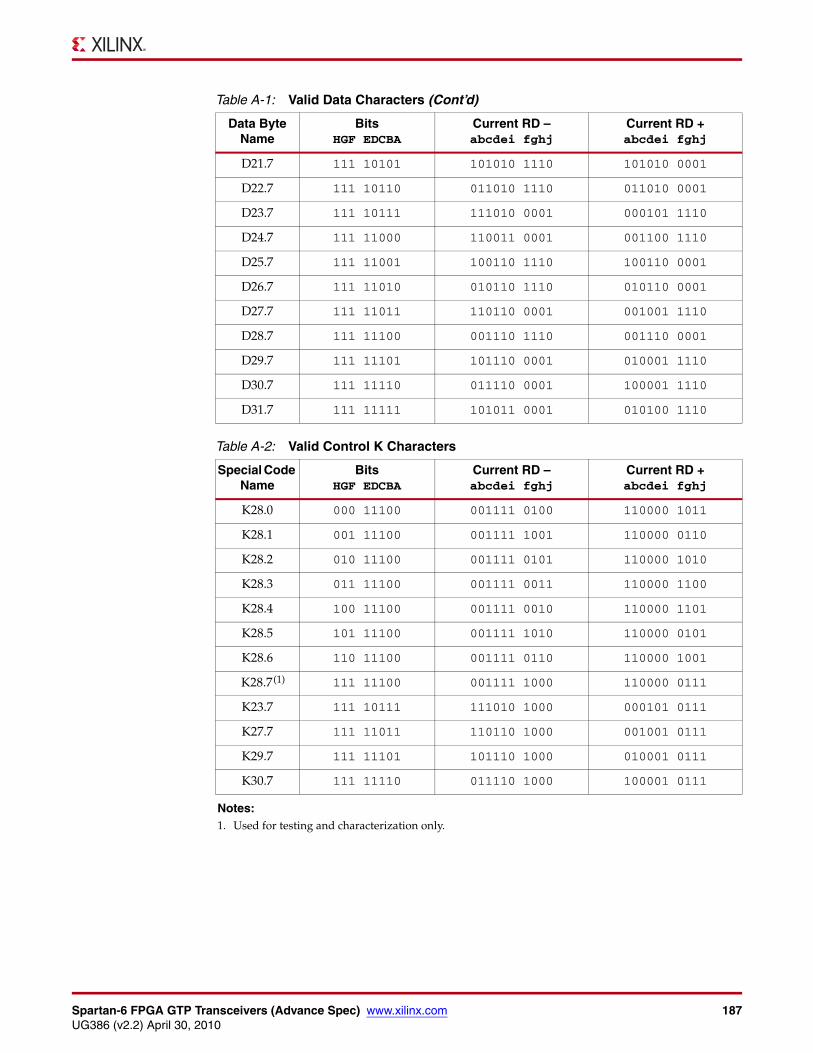
Spartan-6 FPGA GTP Transceivers (Advance Spec) www.xilinx.com 187UG386 (v2.2) April 30, 2010
D21.7 111 10101 101010 1110 101010 0001
D22.7 111 10110 011010 1110 011010 0001
D23.7 111 10111 111010 0001 000101 1110
D24.7 111 11000 110011 0001 001100 1110
D25.7 111 11001 100110 1110 100110 0001
D26.7 111 11010 010110 1110 010110 0001
D27.7 111 11011 110110 0001 001001 1110
D28.7 111 11100 001110 1110 001110 0001
D29.7 111 11101 101110 0001 010001 1110
D30.7 111 11110 011110 0001 100001 1110
D31.7 111 11111 101011 0001 010100 1110
Table A-2: Valid Control K Characters
Special Code Name
Bits HGF EDCBA
Current RD –abcdei fghj
Current RD +abcdei fghj
K28.0 000 11100 001111 0100 110000 1011
K28.1 001 11100 001111 1001 110000 0110
K28.2 010 11100 001111 0101 110000 1010
K28.3 011 11100 001111 0011 110000 1100
K28.4 100 11100 001111 0010 110000 1101
K28.5 101 11100 001111 1010 110000 0101
K28.6 110 11100 001111 0110 110000 1001
K28.7(1) 111 11100 001111 1000 110000 0111
K23.7 111 10111 111010 1000 000101 0111
K27.7 111 11011 110110 1000 001001 0111
K29.7 111 11101 101110 1000 010001 0111
K30.7 111 11110 011110 1000 100001 0111
Notes: 1. Used for testing and characterization only.
Table A-1: Valid Data Characters (Cont’d)
Data Byte Name
Bits HGF EDCBA
Current RD –abcdei fghj
Current RD + abcdei fghj

188 www.xilinx.com Spartan-6 FPGA GTP Transceivers (Advance Spec)UG386 (v2.2) April 30, 2010
Appendix A: 8B/10B Valid Characters
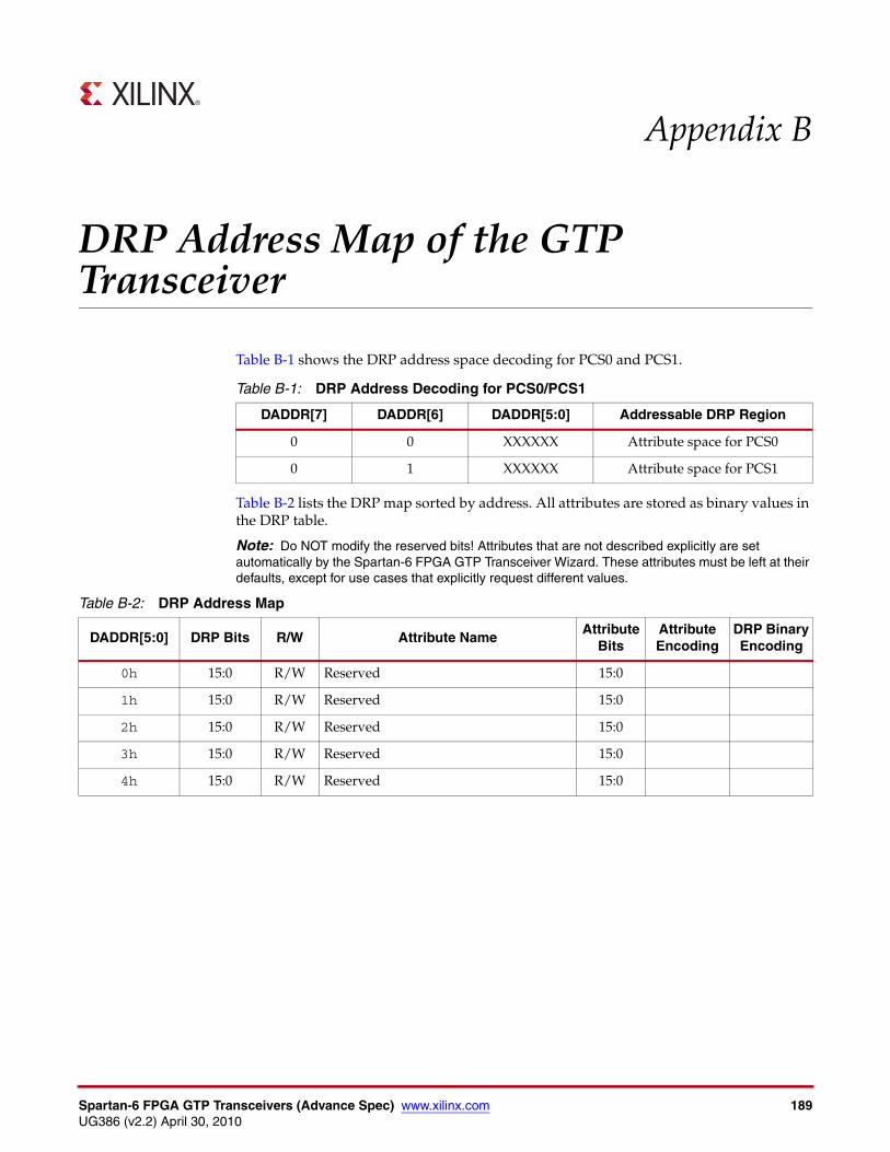
Spartan-6 FPGA GTP Transceivers (Advance Spec) www.xilinx.com 189UG386 (v2.2) April 30, 2010
Appendix B
DRP Address Map of the GTP Transceiver
Table B-1 shows the DRP address space decoding for PCS0 and PCS1.
Table B-2 lists the DRP map sorted by address. All attributes are stored as binary values in the DRP table.
Note: Do NOT modify the reserved bits! Attributes that are not described explicitly are set automatically by the Spartan-6 FPGA GTP Transceiver Wizard. These attributes must be left at their defaults, except for use cases that explicitly request different values.
Table B-1: DRP Address Decoding for PCS0/PCS1
DADDR[7] DADDR[6] DADDR[5:0] Addressable DRP Region
0 0 XXXXXX Attribute space for PCS0
0 1 XXXXXX Attribute space for PCS1
Table B-2: DRP Address Map
DADDR[5:0] DRP Bits R/W Attribute NameAttribute
BitsAttribute Encoding
DRP Binary Encoding
0h 15:0 R/W Reserved 15:0
1h 15:0 R/W Reserved 15:0
2h 15:0 R/W Reserved 15:0
3h 15:0 R/W Reserved 15:0
4h 15:0 R/W Reserved 15:0
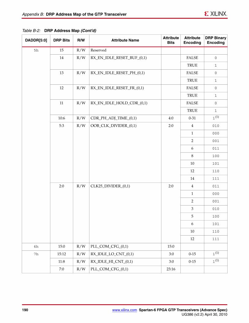
190 www.xilinx.com Spartan-6 FPGA GTP Transceivers (Advance Spec)UG386 (v2.2) April 30, 2010
Appendix B: DRP Address Map of the GTP Transceiver
5h 15 R/W Reserved
14 R/W RX_EN_IDLE_RESET_BUF_(0,1) FALSE 0
TRUE 1
13 R/W RX_EN_IDLE_RESET_PH_(0,1) FALSE 0
TRUE 1
12 R/W RX_EN_IDLE_RESET_FR_(0,1) FALSE 0
TRUE 1
11 R/W RX_EN_IDLE_HOLD_CDR_(0,1) FALSE 0
TRUE 1
10:6 R/W CDR_PH_ADJ_TIME_(0,1) 4:0 0-31 1 (1)
5:3 R/W OOB_CLK_DIVIDER_(0,1) 2:0 4 010
1 000
2 001
6 011
8 100
10 101
12 110
14 111
2:0 R/W CLK25_DIVIDER_(0,1) 2:0 4 011
1 000
2 001
3 010
5 100
6 101
10 110
12 111
6h 15:0 R/W PLL_COM_CFG_(0,1) 15:0
7h 15:12 R/W RX_IDLE_LO_CNT_(0,1) 3:0 0-15 1 (1)
11:8 R/W RX_IDLE_HI_CNT_(0,1) 3:0 0-15 1 (1)
7:0 R/W PLL_COM_CFG_(0,1) 23:16
Table B-2: DRP Address Map (Cont’d)
DADDR[5:0] DRP Bits R/W Attribute NameAttribute
BitsAttribute Encoding
DRP Binary Encoding
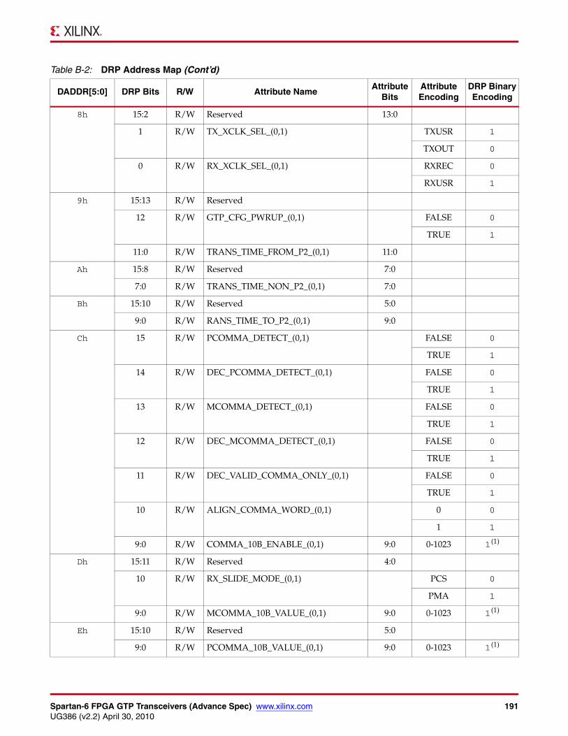
Spartan-6 FPGA GTP Transceivers (Advance Spec) www.xilinx.com 191UG386 (v2.2) April 30, 2010
8h 15:2 R/W Reserved 13:0
1 R/W TX_XCLK_SEL_(0,1) TXUSR 1
TXOUT 0
0 R/W RX_XCLK_SEL_(0,1) RXREC 0
RXUSR 1
9h 15:13 R/W Reserved
12 R/W GTP_CFG_PWRUP_(0,1) FALSE 0
TRUE 1
11:0 R/W TRANS_TIME_FROM_P2_(0,1) 11:0
Ah 15:8 R/W Reserved 7:0
7:0 R/W TRANS_TIME_NON_P2_(0,1) 7:0
Bh 15:10 R/W Reserved 5:0
9:0 R/W RANS_TIME_TO_P2_(0,1) 9:0
Ch 15 R/W PCOMMA_DETECT_(0,1) FALSE 0
TRUE 1
14 R/W DEC_PCOMMA_DETECT_(0,1) FALSE 0
TRUE 1
13 R/W MCOMMA_DETECT_(0,1) FALSE 0
TRUE 1
12 R/W DEC_MCOMMA_DETECT_(0,1) FALSE 0
TRUE 1
11 R/W DEC_VALID_COMMA_ONLY_(0,1) FALSE 0
TRUE 1
10 R/W ALIGN_COMMA_WORD_(0,1) 0 0
1 1
9:0 R/W COMMA_10B_ENABLE_(0,1) 9:0 0-1023 1 (1)
Dh 15:11 R/W Reserved 4:0
10 R/W RX_SLIDE_MODE_(0,1) PCS 0
PMA 1
9:0 R/W MCOMMA_10B_VALUE_(0,1) 9:0 0-1023 1 (1)
Eh 15:10 R/W Reserved 5:0
9:0 R/W PCOMMA_10B_VALUE_(0,1) 9:0 0-1023 1 (1)
Table B-2: DRP Address Map (Cont’d)
DADDR[5:0] DRP Bits R/W Attribute NameAttribute
BitsAttribute Encoding
DRP Binary Encoding
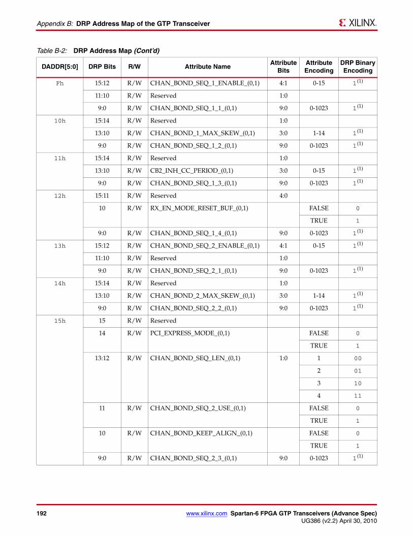
192 www.xilinx.com Spartan-6 FPGA GTP Transceivers (Advance Spec)UG386 (v2.2) April 30, 2010
Appendix B: DRP Address Map of the GTP Transceiver
Fh 15:12 R/W CHAN_BOND_SEQ_1_ENABLE_(0,1) 4:1 0-15 1 (1)
11:10 R/W Reserved 1:0
9:0 R/W CHAN_BOND_SEQ_1_1_(0,1) 9:0 0-1023 1 (1)
10h 15:14 R/W Reserved 1:0
13:10 R/W CHAN_BOND_1_MAX_SKEW_(0,1) 3:0 1-14 1 (1)
9:0 R/W CHAN_BOND_SEQ_1_2_(0,1) 9:0 0-1023 1 (1)
11h 15:14 R/W Reserved 1:0
13:10 R/W CB2_INH_CC_PERIOD_(0,1) 3:0 0-15 1 (1)
9:0 R/W CHAN_BOND_SEQ_1_3_(0,1) 9:0 0-1023 1 (1)
12h 15:11 R/W Reserved 4:0
10 R/W RX_EN_MODE_RESET_BUF_(0,1) FALSE 0
TRUE 1
9:0 R/W CHAN_BOND_SEQ_1_4_(0,1) 9:0 0-1023 1 (1)
13h 15:12 R/W CHAN_BOND_SEQ_2_ENABLE_(0,1) 4:1 0-15 1 (1)
11:10 R/W Reserved 1:0
9:0 R/W CHAN_BOND_SEQ_2_1_(0,1) 9:0 0-1023 1 (1)
14h 15:14 R/W Reserved 1:0
13:10 R/W CHAN_BOND_2_MAX_SKEW_(0,1) 3:0 1-14 1 (1)
9:0 R/W CHAN_BOND_SEQ_2_2_(0,1) 9:0 0-1023 1 (1)
15h 15 R/W Reserved
14 R/W PCI_EXPRESS_MODE_(0,1) FALSE 0
TRUE 1
13:12 R/W CHAN_BOND_SEQ_LEN_(0,1) 1:0 1 00
2 01
3 10
4 11
11 R/W CHAN_BOND_SEQ_2_USE_(0,1) FALSE 0
TRUE 1
10 R/W CHAN_BOND_KEEP_ALIGN_(0,1) FALSE 0
TRUE 1
9:0 R/W CHAN_BOND_SEQ_2_3_(0,1) 9:0 0-1023 1 (1)
Table B-2: DRP Address Map (Cont’d)
DADDR[5:0] DRP Bits R/W Attribute NameAttribute
BitsAttribute Encoding
DRP Binary Encoding
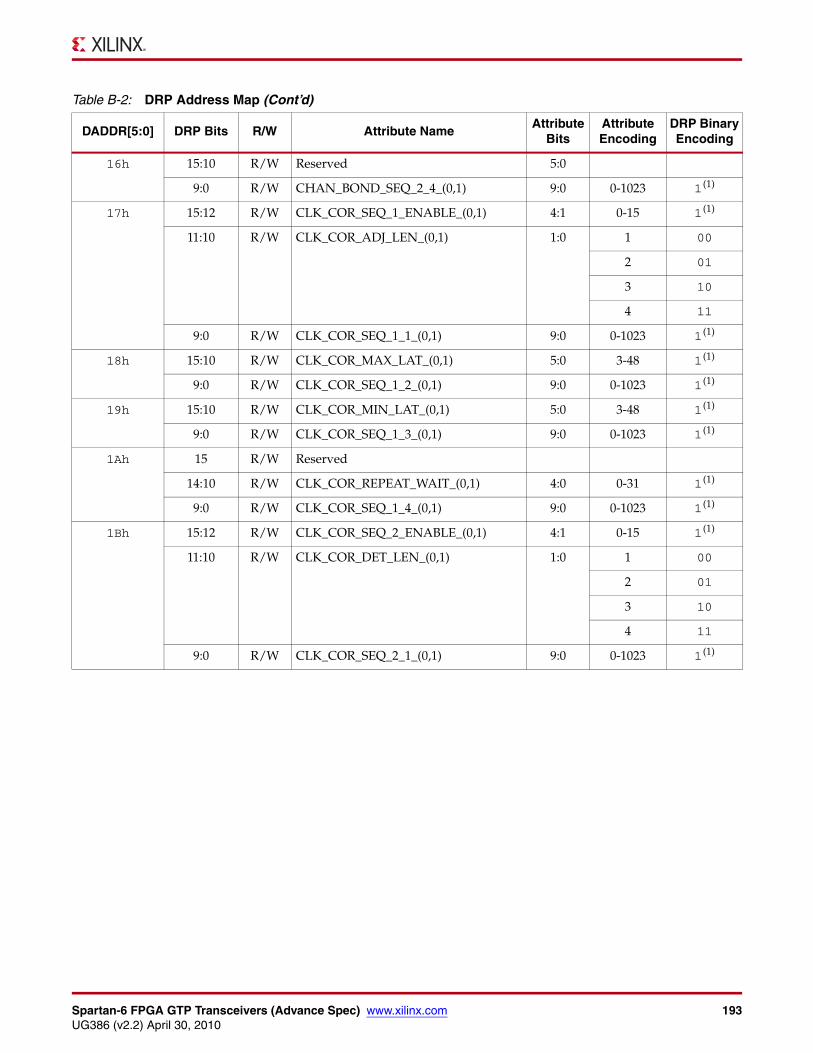
Spartan-6 FPGA GTP Transceivers (Advance Spec) www.xilinx.com 193UG386 (v2.2) April 30, 2010
16h 15:10 R/W Reserved 5:0
9:0 R/W CHAN_BOND_SEQ_2_4_(0,1) 9:0 0-1023 1 (1)
17h 15:12 R/W CLK_COR_SEQ_1_ENABLE_(0,1) 4:1 0-15 1 (1)
11:10 R/W CLK_COR_ADJ_LEN_(0,1) 1:0 1 00
2 01
3 10
4 11
9:0 R/W CLK_COR_SEQ_1_1_(0,1) 9:0 0-1023 1 (1)
18h 15:10 R/W CLK_COR_MAX_LAT_(0,1) 5:0 3-48 1 (1)
9:0 R/W CLK_COR_SEQ_1_2_(0,1) 9:0 0-1023 1 (1)
19h 15:10 R/W CLK_COR_MIN_LAT_(0,1) 5:0 3-48 1 (1)
9:0 R/W CLK_COR_SEQ_1_3_(0,1) 9:0 0-1023 1 (1)
1Ah 15 R/W Reserved
14:10 R/W CLK_COR_REPEAT_WAIT_(0,1) 4:0 0-31 1 (1)
9:0 R/W CLK_COR_SEQ_1_4_(0,1) 9:0 0-1023 1 (1)
1Bh 15:12 R/W CLK_COR_SEQ_2_ENABLE_(0,1) 4:1 0-15 1 (1)
11:10 R/W CLK_COR_DET_LEN_(0,1) 1:0 1 00
2 01
3 10
4 11
9:0 R/W CLK_COR_SEQ_2_1_(0,1) 9:0 0-1023 1 (1)
Table B-2: DRP Address Map (Cont’d)
DADDR[5:0] DRP Bits R/W Attribute NameAttribute
BitsAttribute Encoding
DRP Binary Encoding
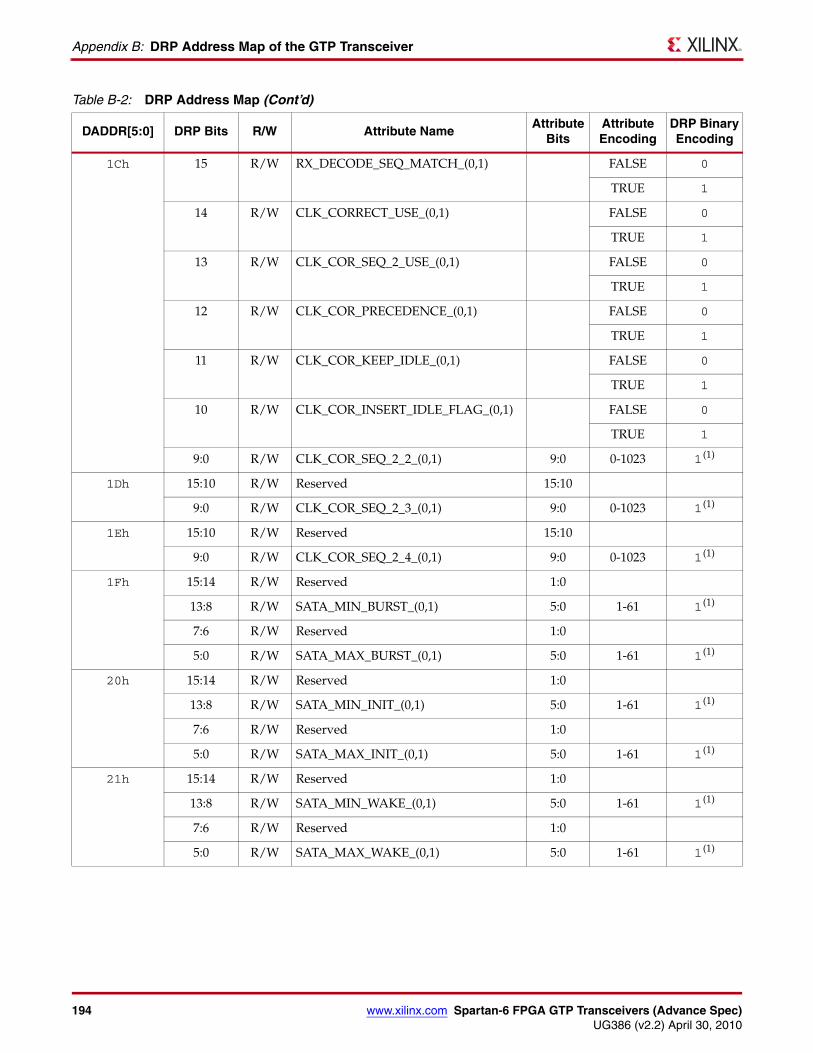
194 www.xilinx.com Spartan-6 FPGA GTP Transceivers (Advance Spec)UG386 (v2.2) April 30, 2010
Appendix B: DRP Address Map of the GTP Transceiver
1Ch 15 R/W RX_DECODE_SEQ_MATCH_(0,1) FALSE 0
TRUE 1
14 R/W CLK_CORRECT_USE_(0,1) FALSE 0
TRUE 1
13 R/W CLK_COR_SEQ_2_USE_(0,1) FALSE 0
TRUE 1
12 R/W CLK_COR_PRECEDENCE_(0,1) FALSE 0
TRUE 1
11 R/W CLK_COR_KEEP_IDLE_(0,1) FALSE 0
TRUE 1
10 R/W CLK_COR_INSERT_IDLE_FLAG_(0,1) FALSE 0
TRUE 1
9:0 R/W CLK_COR_SEQ_2_2_(0,1) 9:0 0-1023 1 (1)
1Dh 15:10 R/W Reserved 15:10
9:0 R/W CLK_COR_SEQ_2_3_(0,1) 9:0 0-1023 1 (1)
1Eh 15:10 R/W Reserved 15:10
9:0 R/W CLK_COR_SEQ_2_4_(0,1) 9:0 0-1023 1 (1)
1Fh 15:14 R/W Reserved 1:0
13:8 R/W SATA_MIN_BURST_(0,1) 5:0 1-61 1 (1)
7:6 R/W Reserved 1:0
5:0 R/W SATA_MAX_BURST_(0,1) 5:0 1-61 1 (1)
20h 15:14 R/W Reserved 1:0
13:8 R/W SATA_MIN_INIT_(0,1) 5:0 1-61 1 (1)
7:6 R/W Reserved 1:0
5:0 R/W SATA_MAX_INIT_(0,1) 5:0 1-61 1 (1)
21h 15:14 R/W Reserved 1:0
13:8 R/W SATA_MIN_WAKE_(0,1) 5:0 1-61 1 (1)
7:6 R/W Reserved 1:0
5:0 R/W SATA_MAX_WAKE_(0,1) 5:0 1-61 1 (1)
Table B-2: DRP Address Map (Cont’d)
DADDR[5:0] DRP Bits R/W Attribute NameAttribute
BitsAttribute Encoding
DRP Binary Encoding
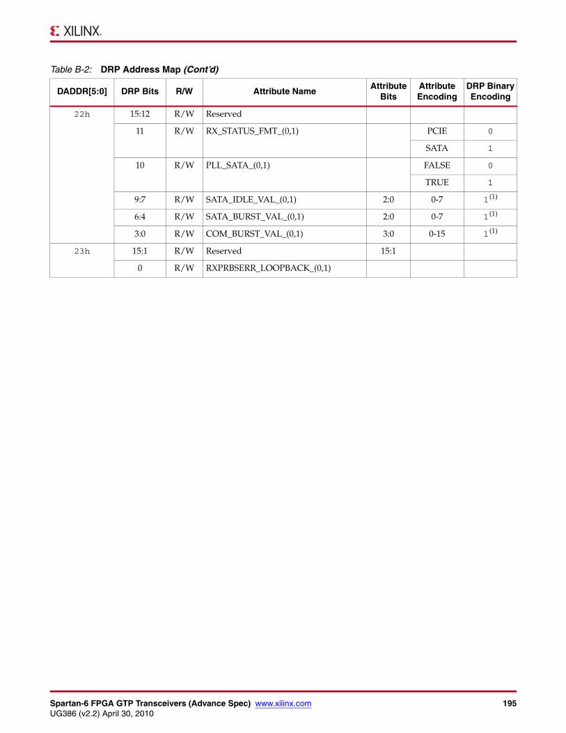
Spartan-6 FPGA GTP Transceivers (Advance Spec) www.xilinx.com 195UG386 (v2.2) April 30, 2010
22h 15:12 R/W Reserved
11 R/W RX_STATUS_FMT_(0,1) PCIE 0
SATA 1
10 R/W PLL_SATA_(0,1) FALSE 0
TRUE 1
9:7 R/W SATA_IDLE_VAL_(0,1) 2:0 0-7 1 (1)
6:4 R/W SATA_BURST_VAL_(0,1) 2:0 0-7 1 (1)
3:0 R/W COM_BURST_VAL_(0,1) 3:0 0-15 1 (1)
23h 15:1 R/W Reserved 15:1
0 R/W RXPRBSERR_LOOPBACK_(0,1)
Table B-2: DRP Address Map (Cont’d)
DADDR[5:0] DRP Bits R/W Attribute NameAttribute
BitsAttribute Encoding
DRP Binary Encoding
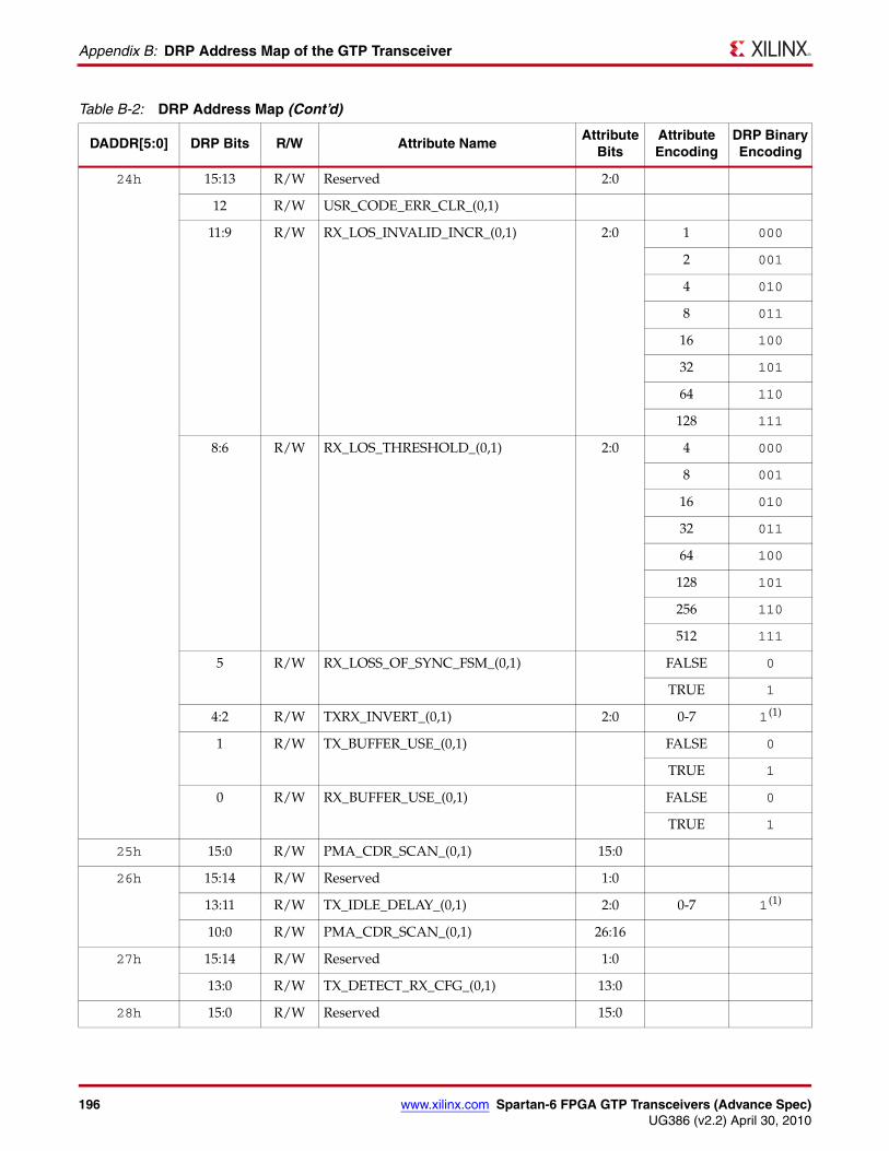
196 www.xilinx.com Spartan-6 FPGA GTP Transceivers (Advance Spec)UG386 (v2.2) April 30, 2010
Appendix B: DRP Address Map of the GTP Transceiver
24h 15:13 R/W Reserved 2:0
12 R/W USR_CODE_ERR_CLR_(0,1)
11:9 R/W RX_LOS_INVALID_INCR_(0,1) 2:0 1 000
2 001
4 010
8 011
16 100
32 101
64 110
128 111
8:6 R/W RX_LOS_THRESHOLD_(0,1) 2:0 4 000
8 001
16 010
32 011
64 100
128 101
256 110
512 111
5 R/W RX_LOSS_OF_SYNC_FSM_(0,1) FALSE 0
TRUE 1
4:2 R/W TXRX_INVERT_(0,1) 2:0 0-7 1 (1)
1 R/W TX_BUFFER_USE_(0,1) FALSE 0
TRUE 1
0 R/W RX_BUFFER_USE_(0,1) FALSE 0
TRUE 1
25h 15:0 R/W PMA_CDR_SCAN_(0,1) 15:0
26h 15:14 R/W Reserved 1:0
13:11 R/W TX_IDLE_DELAY_(0,1) 2:0 0-7 1 (1)
10:0 R/W PMA_CDR_SCAN_(0,1) 26:16
27h 15:14 R/W Reserved 1:0
13:0 R/W TX_DETECT_RX_CFG_(0,1) 13:0
28h 15:0 R/W Reserved 15:0
Table B-2: DRP Address Map (Cont’d)
DADDR[5:0] DRP Bits R/W Attribute NameAttribute
BitsAttribute Encoding
DRP Binary Encoding
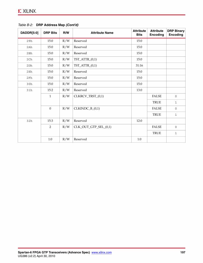
Spartan-6 FPGA GTP Transceivers (Advance Spec) www.xilinx.com 197UG386 (v2.2) April 30, 2010
29h 15:0 R/W Reserved 15:0
2Ah 15:0 R/W Reserved 15:0
2Bh 15:0 R/W Reserved 15:0
2Ch 15:0 R/W TST_ATTR_(0,1) 15:0
2Dh 15:0 R/W TST_ATTR_(0,1) 31:16
2Eh 15:0 R/W Reserved 15:0
2Fh 15:0 R/W Reserved 15:0
30h 15:0 R/W Reserved 15:0
31h 15:2 R/W Reserved 13:0
1 R/W CLKRCV_TRST_(0,1) FALSE 0
TRUE 1
0 R/W CLKINDC_B_(0,1) FALSE 0
TRUE 1
32h 15:3 R/W Reserved 12:0
2 R/W CLK_OUT_GTP_SEL_(0,1) FALSE 0
TRUE 1
1:0 R/W Reserved 1:0
Table B-2: DRP Address Map (Cont’d)
DADDR[5:0] DRP Bits R/W Attribute NameAttribute
BitsAttribute Encoding
DRP Binary Encoding
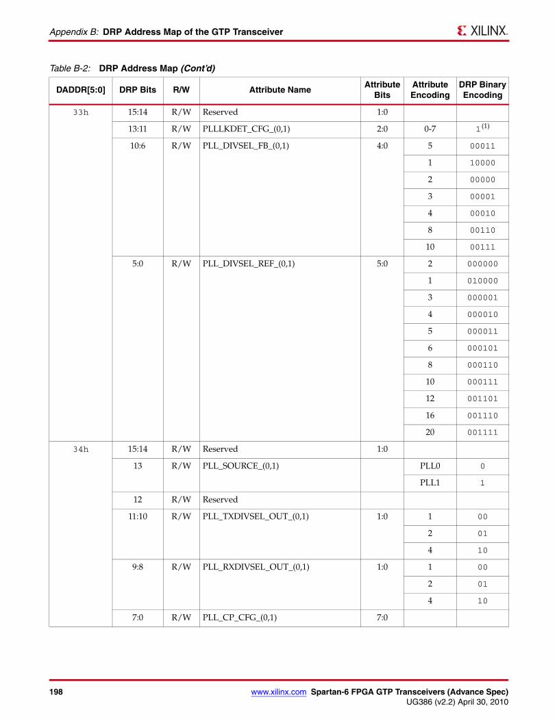
198 www.xilinx.com Spartan-6 FPGA GTP Transceivers (Advance Spec)UG386 (v2.2) April 30, 2010
Appendix B: DRP Address Map of the GTP Transceiver
33h 15:14 R/W Reserved 1:0
13:11 R/W PLLLKDET_CFG_(0,1) 2:0 0-7 1 (1)
10:6 R/W PLL_DIVSEL_FB_(0,1) 4:0 5 00011
1 10000
2 00000
3 00001
4 00010
8 00110
10 00111
5:0 R/W PLL_DIVSEL_REF_(0,1) 5:0 2 000000
1 010000
3 000001
4 000010
5 000011
6 000101
8 000110
10 000111
12 001101
16 001110
20 001111
34h 15:14 R/W Reserved 1:0
13 R/W PLL_SOURCE_(0,1) PLL0 0
PLL1 1
12 R/W Reserved
11:10 R/W PLL_TXDIVSEL_OUT_(0,1) 1:0 1 00
2 01
4 10
9:8 R/W PLL_RXDIVSEL_OUT_(0,1) 1:0 1 00
2 01
4 10
7:0 R/W PLL_CP_CFG_(0,1) 7:0
Table B-2: DRP Address Map (Cont’d)
DADDR[5:0] DRP Bits R/W Attribute NameAttribute
BitsAttribute Encoding
DRP Binary Encoding
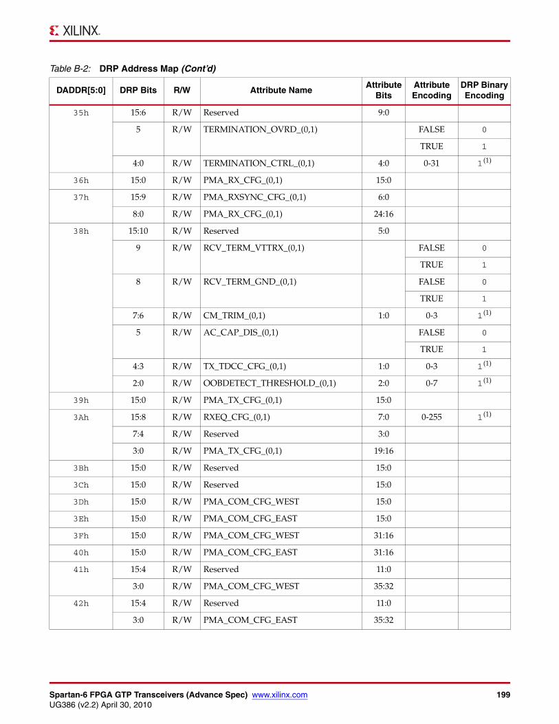
Spartan-6 FPGA GTP Transceivers (Advance Spec) www.xilinx.com 199UG386 (v2.2) April 30, 2010
35h 15:6 R/W Reserved 9:0
5 R/W TERMINATION_OVRD_(0,1) FALSE 0
TRUE 1
4:0 R/W TERMINATION_CTRL_(0,1) 4:0 0-31 1 (1)
36h 15:0 R/W PMA_RX_CFG_(0,1) 15:0
37h 15:9 R/W PMA_RXSYNC_CFG_(0,1) 6:0
8:0 R/W PMA_RX_CFG_(0,1) 24:16
38h 15:10 R/W Reserved 5:0
9 R/W RCV_TERM_VTTRX_(0,1) FALSE 0
TRUE 1
8 R/W RCV_TERM_GND_(0,1) FALSE 0
TRUE 1
7:6 R/W CM_TRIM_(0,1) 1:0 0-3 1 (1)
5 R/W AC_CAP_DIS_(0,1) FALSE 0
TRUE 1
4:3 R/W TX_TDCC_CFG_(0,1) 1:0 0-3 1 (1)
2:0 R/W OOBDETECT_THRESHOLD_(0,1) 2:0 0-7 1 (1)
39h 15:0 R/W PMA_TX_CFG_(0,1) 15:0
3Ah 15:8 R/W RXEQ_CFG_(0,1) 7:0 0-255 1 (1)
7:4 R/W Reserved 3:0
3:0 R/W PMA_TX_CFG_(0,1) 19:16
3Bh 15:0 R/W Reserved 15:0
3Ch 15:0 R/W Reserved 15:0
3Dh 15:0 R/W PMA_COM_CFG_WEST 15:0
3Eh 15:0 R/W PMA_COM_CFG_EAST 15:0
3Fh 15:0 R/W PMA_COM_CFG_WEST 31:16
40h 15:0 R/W PMA_COM_CFG_EAST 31:16
41h 15:4 R/W Reserved 11:0
3:0 R/W PMA_COM_CFG_WEST 35:32
42h 15:4 R/W Reserved 11:0
3:0 R/W PMA_COM_CFG_EAST 35:32
Table B-2: DRP Address Map (Cont’d)
DADDR[5:0] DRP Bits R/W Attribute NameAttribute
BitsAttribute Encoding
DRP Binary Encoding

200 www.xilinx.com Spartan-6 FPGA GTP Transceivers (Advance Spec)UG386 (v2.2) April 30, 2010
Appendix B: DRP Address Map of the GTP Transceiver


![Multiband Transceivers - [Chapter 6] Multi-mode and Multi-band Transceivers](https://img.pdfslide.net/doc/110x75/55cd229ebb61ebba378b468a/multiband-transceivers-chapter-6-multi-mode-and-multi-band-transceivers.jpg)