Embed Size (px)
Citation preview
Journal of Electron Spectroscopy and Related Phenomena 124 (2002) 263–279www.elsevier.com/ locate /elspec
Spin-polarized Fermi surface mappinga,b , a c a,b a*M. Hoesch , T. Greber , V.N. Petrov , M. Muntwiler , M. Hengsberger ,
a a¨W. Auwarter , J. Osterwaldera ¨ ¨ ¨Physik-Institut, Winterthurerstr. 190, Universitat Zurich-Irchel, 8057 Zurich, Switzerland
bSLS Project, Paul Scherrer Institut, 5232 Villigen PSI, SwitzerlandcSt. Petersburg Technical University, 29 Polytechnicheskaya Street, 195251 St Petersburg, Russia
Received 9 December 2001; received in revised form 22 December 2001; accepted 21 January 2002
Abstract
The magnetic and electronic properties of itinerant ferromagnets and their interplay have been studied in the last few yearsby spin resolved electron spectroscopy on one hand and by high-resolution angle-resolved photoemission experiments on theother. We discuss how the two approaches can be combined in a high resolution electron spectrometer with spin resolutionfor angle-scanned Fermi surface mapping experiments. We have built this new instrument, which allows an advance into adeeper understanding of magnetic thin film or multilayer systems, where band structures become intricately dense inmomentum space and where the magnetization direction can change from layer to layer. Spin-resolution is thus required toarrive at a correct assignment of spectral features. A fully three-dimensional polarimeter makes the instrument ‘complete’ inthe sense that all properties of the photoelectron are measured. First experiments on Ni(111) conclusively confirm previousband and spin assignments at the Fermi level and demonstrate the correct functioning of the apparatus. 2002 ElsevierScience B.V. All rights reserved.
Keywords: Photoemission; Itinerant ferromagnetism; Magnetic multilayers; Spin polarization; Fermi surface; Nickel; Surface electronicstructure; Interface effects
1. Introduction structures have opened the promising field of mag-netoelectronics or spintronics [2]. While the prepara-
Recent advances in physics, chemistry and materi- tion of laterally structured devices is still in itsals science have made it possible to produce artificial infancy, the production of layered artificial struc-magnetic materials, i.e. materials that are far away tures, that can be prepared by sophisticated growthfrom thermal equilibrium and do not exist in nature. methods, has matured in recent years. Multilayers ofThey are often structured on the nanometer scale, alternating magnetic and non-magnetic metals areand there is increasing evidence that electronic and now finding their way into the markets as sensors inmagnetic properties can be tailored by controlling the magnetic recording heads.structuring [1]. New ideas for devices based on such In order to obtain a fundamental understanding of
such systems and how their properties can beengineered, we need to have a detailed picture of*Corresponding author. Tel.: 141-1-635-5824; fax: 141-1-635-their electronic structure and how it varies when the5704.
E-mail address: [email protected] (M. Hoesch). artificial structuring is changed. Of particular impor-
0368-2048/02/$ – see front matter 2002 Elsevier Science B.V. All rights reserved.PI I : S0368-2048( 02 )00058-0
264 M. Hoesch et al. / Journal of Electron Spectroscopy and Related Phenomena 124 (2002) 263 –279
tance are the electrons near the Fermi energy and inferred from comparing the measured Fermi surfacetheir momentum distribution, i.e. the Fermi surface. contours to those obtained from a band structureIn magnetic multilayers, e.g. a clear correlation has calculation. The excellent agreement between thebeen found between Fermi level crossings of quan- two made the assignment unambiguous [9,10].tum well states, which can be tuned by varying the It should be pointed out that for the case of a bulkinterlayer thickness, and the oscillatory coupling ferromagnet like Ni metal one does not need to(ferromagnetic vs. antiferromagnetic) between the magnetize the sample in order to see the spin-splitmagnetic layers [3]. The classical Fermi surface Fermi surfaces, because the local magnetization inprobes, such as the de-Haas-van-Alphen effect, each magnetic domain induces the same exchangepositron annihilation or Compton scattering, cannot splitting throughout the crystal, except for minorbe used for these kinds of samples because they are regions inside domain walls. Minority and majorityessentially bulk probes. On the other hand, Fourier spin character has thus a local meaning even thoughanalysis of scanning-tunneling microscopy/spectros- the sample as a whole is unmagnetized. However, incopy images, which was recently introduced as a nanostructured materials such as e.g. magnetic multi-new Fermi surface probe [4], has been demonstrated layers, it is crucial to identify the relative spinonly for surface states on noble metal and simple character of electronic bands in the various magneticmetal surfaces, and it lacks momentum resolution layers as well as the spin polarization of sp-bands ofperpendicular to the layer plane. Angle-resolved the non-magnetic layers. For this purpose, a spin-photoemission (ARUPS) thus remains as the prime resolved photoemission or inverse photoemissiontechnique to study the electronic structure and the experiment must be carried out. Unfortunately, theFermi surface of such nanostructured magnetic sam- measurement of the photoelectron spin polarizationples, where quantized bulk states are believed to play is very cumbersome, with typical devices (Mott
23a crucial role for the magnetic coupling between detectors) having an overall efficiency of 10 to24magnetic layers. 10 compared to common spin-averaging detectors
The traditional procedure in ARUPS experiments [11]. In order to make up for the reduced sensitivity,was to locate Fermi level crossings of energy bands spin-resolved experiments usually have to makein angle-resolved photoemission spectra in order to strong compromises in energy and angular resolu-trace Fermi surface contours [5]. Recently, a few tion, and one thus sacrifices the wealth of infor-groups have begun to map Fermi surfaces directly by mation near the Fermi level available with high-measuring intensities of photoelectrons emitted from resolution photoemission [12].the Fermi edge as a function of emission angles In magnetic nanostructures, such as e.g. multi-relative to the crystal axes, and thus of the momen- layers, the presence of new boundary conditions or→tum component k parallel to the surface [6,7]. At new periodicities of the order of one nanometeri
positions where a band crosses the Fermi level, the makes those dimensions in reciprocal space becomephotoemission intensity at the Fermi edge rises smaller by typically one order of magnitude. This issharply, contributing to the measured contour of the illustrated in Fig. 1. An idealized Co Cu (111)5 4
Fermi surface map. It has been demonstrated that magnetic multilayer is depicted in (a), which has athis procedure produces accurate bulk and surface superperiodicity of nine atomic layers in the verticalFermi surface maps of noble metals, magnetic transi- direction. Fig. 1b shows the Fermi surface contourstion metals and even high-temperature superconduc- of bulk Cu and of face-centered-cubic (fcc) bulk Co
¯ ¯tors [8]. A demonstration of the potential of photo- (majority spin) within the (112) plane of the fccemission mapping as applied to a magnetic system reciprocal lattice. Slab calculations for the multilayerhas recently been given. The Fermi surfaces of both [13] produce the closely spaced Fermi surface sheetsminority and majority electrons in ferromagnetic Ni that are plotted inside the vertically compressedmetal have been measured, as well as their behavior hexagonal Brillouin zone. The extended zone schemewith temperature as the Curie temperature is ap- for the multilayer will thus show a very denseproached and exceeded. In this case, the spin charac- manifold of Fermi surface sheets. As is outlined inter of the bands was not measured directly but was Section 2, this leads to closely spaced Fermi surface
M. Hoesch et al. / Journal of Electron Spectroscopy and Related Phenomena 124 (2002) 263 –279 265
Fig. 1. (a) Schematic section through a magnetic multilayer consisting of an alternative stacking of five monolayers (ML) of fcc Co and 4ML of Cu. (b) Cuts through Fermi surfaces of bulk copper, majority bulk cobalt, and through the majority Fermi surface of the periodic
] ]Co Cu (111) multilayer of (a). The labels G and K refer to points at the center and corners, respectively, of the hexagonal two-dimensional5 4
Brillouin zone of the multilayer, while G, K and L refer to high-symmetry points in the three-dimensional Brillouin zone of the fcc lattice. ki
and k are expressed in units of 2p /a, where a is the fcc lattice constant (from Ref. [13]).'
contours in photoemission Fermi surface maps. This One can thus conveniently take a spin-averagedexample shows that high momentum resolution is a global map of Fermi surface contours before homingprerequisite in order to obtain relevant Fermi surface in on selected contours for polarization analysis. Thedata for such systems and that it must not be second obstacle is more fundamental: a spincompromised when spin detection is employed. polarimeter based on Mott scattering can measure the
We have thus designed and built a new spin- and spin polarization of photoelectrons along two axesangle-resolved photoemission spectrometer that that are fixed in space (see Section 3). Unfortunatelyshould meet the specifications required for measuring this is not sufficient. The measurement of Fermispin-resolved Fermi surfaces at sufficiently high surface maps requires free rotation of the sample,energy and angular resolution. In doing so we had to and of its magnetization direction, about two in-overcome two major obstacles: (i) the sensitivity dependent axes. In order to trace the polarizationproblem and (ii) the magnetization direction prob- vector of the electrons throughout the complete map,lem. The sensitivity problem due to the low detection one has thus to measure all three spin components.efficiency of current spin polarimeters is solved We have chosen a design based on two completeusing high flux synchrotron light from a third-gene- Mott polarimeters, thus measuring altogether fourration source for excitation, and by combining spin- spin projections (see Section 4). The one redundantresolved and spin-averaged photoelectron spectros- projection is selected to provide a useful cross checkcopy simultaneously in the same electron analyzer. for the spin polarization along one fixed axis. Since
266 M. Hoesch et al. / Journal of Electron Spectroscopy and Related Phenomena 124 (2002) 263 –279
all quantum numbers of a photoelectron—momen- surface potential step (step 3), which is characterizedtum and spin—are measured in this spectrometer, it by the inner potential V , can then be treated like a0
can be regarded as complete, hence the name COm- refraction at the boundary of two media: the free-plete PHotoEmission Experiment (COPHEE). A electron plane wave outside the surface has a shortersimilar design has been described by Chen [14]. k than the one inside the solid.'
The interest in spin-resolved Fermi surface map- From the measured photoelectron kinetic energy inping is not limited to magnetic nanostructures. There vacuumare several other pressing fundamental problems in
mE 5 hn 2 F 2 E (1)solid state physics and surface science where this kin B
new spectrometer can bring significant advances. Forwhere hn, F and E are photon energy, workinstance, the spin-polarization of majority and mi- B
function and binding energy measured from thenority Fermi surface contours on nickel can beFermi level, respectively, and from the emissionmeasured as the Curie temperature is approachedpolar angle q (measured from the surface normal),from below, and the interplay between magnetic m
one calculates readilyfluctuations and the magnetic exchange splitting canbe studied in detail [10]. Manybody-effects lead to
→ 1 ]]mstrong momentum and spin-dependent band shifts ]uk u 5 2mE sin q (2)œi kin m"and band broadening in measured photoemissionspectra from the late 3d transition metals, even near andthe Fermi energy, compared to single-particle bandstructure calculations [15,16]. In cases where de- 1 ]]]]m]k 5 2m(E 1V ) cos q (3)œtailed manybody calculations are not available, such ' kin 0"as, e.g. in alloys, the measurement of the electronspin is therefore very important for a correct assign- wherement of the observed bands.
]]]mEkin]]]sinq 5 sin q (4)mm E 1Vœ kin 0
2. Fermi surface mapping by photoemission is the sine of the refracted polar angle. Within thefree-electron final-state approximation, these com-
→Fermi surface mapping requires the measurement→ ponents define the k -vector of the photo-hole inside
of the electron momentum, or wave vector k , which the solid for a particular sample azimuth w. Mattersis complicated by the fact that photoemission from become simpler in two-dimensional systems such as
→crystalline surfaces conserves only the wave vector→ surface states or ultrathin films, where only k isicomponent k parallel to the surface. The shorti relevant [20].
probing depth and the propagation through the Constant energy maps or, more specifically, Fermisurface potential step broadens and reduces, respec- surface maps result from taking photoemission inten-tively, the wave vector component k perpendicular' sities at just one binding energy and scanning bothto the surface. Photoemission calculations within the emission angles over most of the hemisphere aboveone-step model [17] considering appropriate time- the surface [7]. According to Eqs. (2) and (3), andreversed low-energy electron diffraction (LEED) including the rotation about the azimuthal angle w,
→states as photoelectron final states can overcome this the sampled k -vectors then sweep the surface of aproblem quantitatively. On the other hand, the much spherical sector with a radius as described bysimpler three-step model [18] has proved quitesuccessful when free-electron final states are used for 1 ]]]]m]k 5 2m(E 1V ) (5)œdescribing the electron propagation through the solid kin 0"to the surface (step 2) after the photoexcitationprocess (step 1) [19]. Transmission through the and with its opening angle reduced by refraction
M. Hoesch et al. / Journal of Electron Spectroscopy and Related Phenomena 124 (2002) 263 –279 267
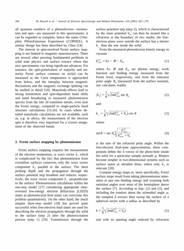
effects compared to the polar angle range measured stant energy surfaces (initial and final state) with theoutside the crystal. proper energy separation intersect, as is shown for
¯This is illustrated in Fig. 2, which shows the (110) the case of the Fermi surface of nickel. It is requiredplane in the reciprocal space of fcc Ni. The free- that the photoelectron picks up momentum from theelectron final states for excitation with He I (21.21 lattice in the form of a reciprocal lattice vector. IneV) and He II (40.8 eV) appear as circles centered at the actual measurement, these intersections formG in this plot, and the photoemission horizon, continuous contours on a grey scale plot (see e.g.000
above which electrons can overcome the surface Fig. 3a), because the constant energy surfaces arepotential barrier, is indicated by the horizontal continuous in three-dimensional momentum space.hatched line. Photoelectrons outside the surface will The resulting Fermi surface contours can also bebe measured at higher polar angles due to the produced by applying the same intersection pro-refraction described in Eq. (4). In the extended zone cedure to a band structure calculation. Fig. 3bscheme of Fig. 2, momentum conservation in the demonstrates how well the experimental contoursphotoemission process means that transitions for a can be matched in the case of Ni, in this case for agiven photon energy occur wherever the two con- measurement through the (111) surface. The agree-
Fig. 2. Schematic diagram for k-space mapping experiments. In the free electron final state approximation direct transitions are expected if→
the final state sphere intersects with an initial state band in the extended zone scheme. k of these intersection points is conserved throughouti
the whole photoemission process. The photoemission horizon (hatched line) is imposed by the inner potential, which has to be overcome bythe photoelectron travelling into vacuum.
268 M. Hoesch et al. / Journal of Electron Spectroscopy and Related Phenomena 124 (2002) 263 –279
3. Spin polarimetry in three dimensions
To measure the spin polarization of electrons, alarge variety of polarimeters have been devised sincethe discovery of the electron’s magnetic moment.The classical method goes back to Mott’s analysis ofthe elastic scattering of relativistic electrons withatomic nuclei [22], which predicted an asymmetry inthe backscattered intensities N , N measured on theL R
left and right of the incoming beam in a commonscattering plane. The polarization component P inx
the direction perpendicular to the scattering plane isdetermined from the asymmetry
(N 2 N )L R]]]A 5 (6)x (N 1 N )L R
and the so-called Sherman function S [23] as
P 5 A /S (7)x x
The Sherman function is the asymmetry that wouldbe measured in the case of a 100% polarized beam.It determines the analyzing power of the process andof the detection geometry. The overall efficiency of apolarimeter can be judged from the figure of merit
2´ 5 (I /I )S (8)0
where I /I is the ratio of detected electrons to the0
total number of incoming electrons [24]. The statisti-cal error due to the electron counting can be found as
]]]DA 5 1/ N 1 N (9)œx L R
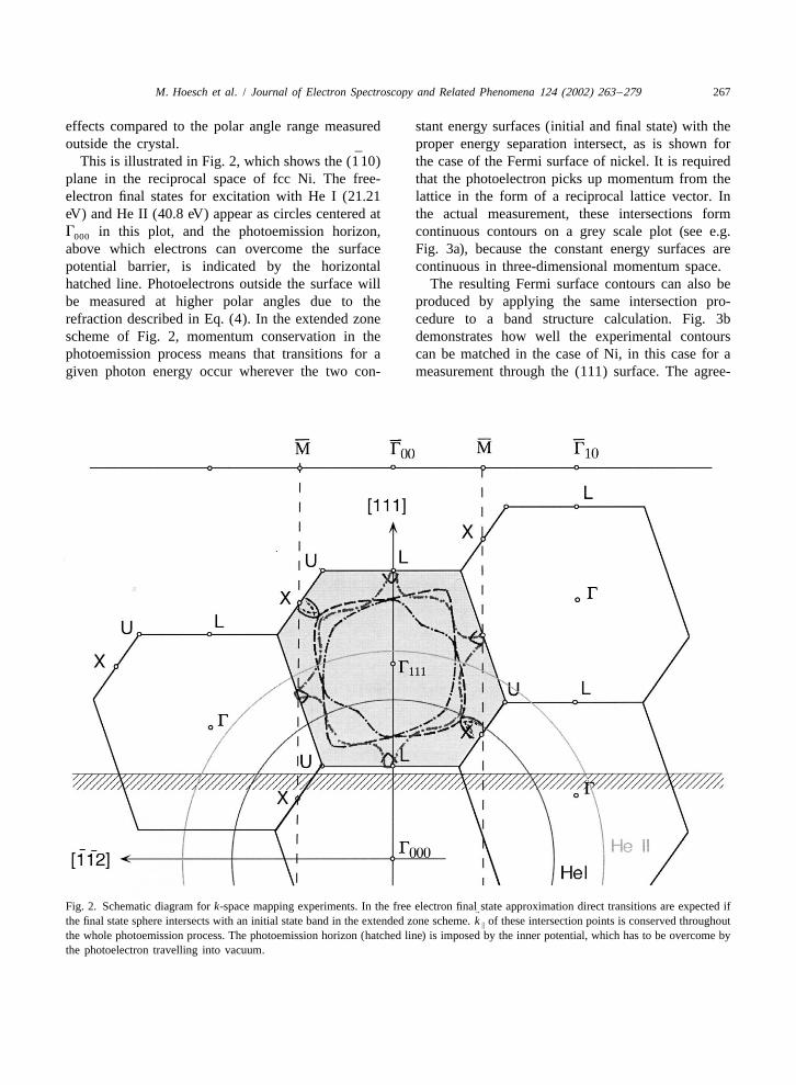
For a given number N of incoming electrons, the0 ]statistical error of P is thus given by DP 5 1/ ´N .œx x 0Fig. 3. (a) He Ia excited Fermi surface map (hn 521.21 eV) from→ In this sense, the figure of merit corresponds to theNi(111). A k projection of the raw data is presented in a linearidetection efficiency for spin polarization. Typicalgrey scale, with highest intensities in white, lowest in black. In (b)
24 23figures range between ´ 5 10 and ´ 5 10 .the corresponding spin-polarized band structure calculation is→
displayed, showing Fermi level crossings at the same k locations The scattering plane is spanned by the incomingi
as in the measurement (a). Majority spin bands are shown in beam and the positions of the detectors for left andblack, minority spin bands in grey. The region highlighted by a
right scattering. In a single polarimeter it is thereforeblack arrow is discussed in Section 5 (figure from Ref. [21]).possible to measure the two transverse polarizationcomponents of an electron beam by arranging fourdetectors in two orthogonal scattering planes in front
ment is good enough to permit the assignment of the of the target.majority /minority character of the individual con- In a real Mott polarimeter, the electrons have to betours. accelerated to relativistic energies and then detected
M. Hoesch et al. / Journal of Electron Spectroscopy and Related Phenomena 124 (2002) 263 –279 269
in an energy sensitive way to filter the signal from Electron Diffraction (LEED) scattering, where theinelastically scattered electrons, which would other- left–right detectors collect the signal from twowise wash out the polarization sensitivity. The basic equivalent diffraction spots from a tungsten singlephysical process which is responsible for the differ- crystal surface [32]. Also in diffuse scattering fromence between backscattering to the left and the right Au surfaces at low energies a good figure of meritis the spin–orbit interaction in the potential of the has been demonstrated because of the high totalatomic nucleus. The effect is stronger the heavier the reflectivity for slow electrons [33], and thesetarget nuclei, and gold foils represent an optimum polarimeters, also measuring a left–right asymmetrycompromise between high atomic number and target of reflected electrons, have been successfully em-inertness. ployed for electron spectroscopy applications. Due to
For our experiment we chose a polarimeter [25] in the high surface sensitivity at low energies, thesewhich the electrostatic acceleration voltage is 60 kV polarimeters require frequent conditioning of theand the detectors are energy sensitive silicon diodes scattering target, and the performance is subject tooperated in reverse bias with a variable discriminator continuous change even in good vacuum.threshold. The detectors with the amplifiers and In addition to polarimeters based on backscatter-discriminators are floated on top of the acceleration ing, a number of other effects in the interaction ofvoltage to allow a field-free travel of the electrons polarized electrons with solids have been employedfrom the scattering gold foil to the detectors. The for polarimetry. An absorption detector measures theacceleration field is provided by two concentric spin-dependent absorption on a metal surface [11]. Ahemispheres thereby giving a highly focusing spheri- promising recent development are transmission de-cal field. These two electron optical features reduce tectors based on the spin filter effect of a ferromag-the polarimeter’s sensitivity to slight motions or netic film. The high analyzing power of the spinchanges in shape of the incoming beam [26]. The filtering based on the exchange interaction can leaddesign of these polarimeters goes back to the classi-
to a very high figure of merit. For practical applica-cal Mott polarimeters operating at 100 to 120 keV
tions, the total transmission still needs to be im-[27], yet they can be combined with a conventional
proved. It is limited by the large amount of supportenergy analyzer due to their compactness.
material needed to make the films free standing.A second class of Mott polarimeters re-deceleratesAll polarimeters based on scattering have thethe electrons to near ground potential after the
common limitation that they can only detect the twoscattering, using a retarding field which can only bepolarization components transverse to the incomingovercome by the elastically scattered electrons.beam. In an electrostatic beam deflection system theThese detectors, named mini-Mott polarimeters, canspin remains fixed in space from the sample to thework at much lower accelerating voltages of typical-detector. If a certain polarization component in thely 25 kV and can be more easily combined withsample is to be analyzed, the orientation of thespectroscopic equipment. The development of thesedetector has to be chosen accordingly. The completedevices [28,29] is very advanced and detailed nu-three-dimensional polarization vector can be ana-merical analyses have been employed for theirlyzed by sending the electrons to two independent,optimization [30,31]. The electron optical acceptanceorthogonally mounted polarimeters. This concept isis very high, but the fact that the filtering ofshown schematically in Fig. 4. In this design, theinelastically scattered electrons is also based onpolarization component P along the entrance lenselectron optics makes them sensitive to the condition z
axis of the analyzer, i.e. the longitudinal polarizationof the incoming beam, which can give rise toof the photoelectrons, is covered by both polarime-spurious effects in a scanned experiment [26].ters, a redundancy which can be used to enhance theIn addition to these polarimeters operating atsensitivity in this component and to cross-check inrelativistic energies, which can truly be called Mottthe course of data taking. If we label the eightdetectors, there is also a class of polarimeters baseddetectors according to Fig. 4 we find the fullon scattering at lower kinetic energies. Very high →
efficiencies have been achieved by Low Energy polarization vector P as
270 M. Hoesch et al. / Journal of Electron Spectroscopy and Related Phenomena 124 (2002) 263 –279
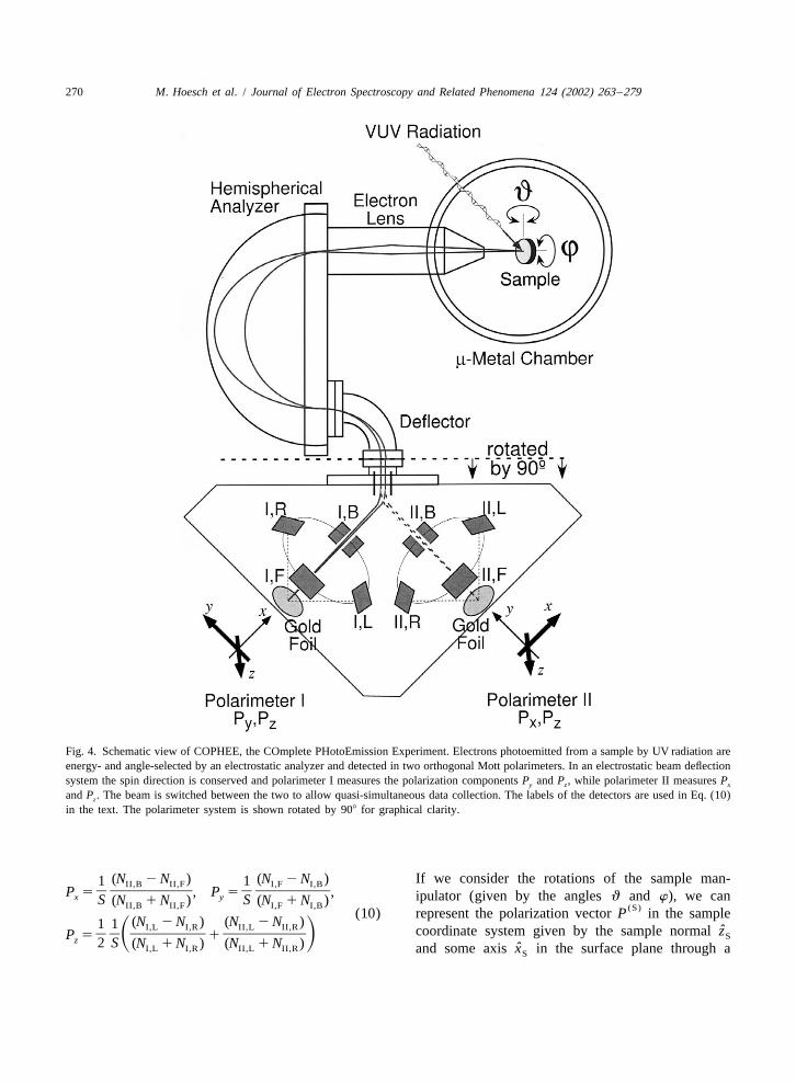
Fig. 4. Schematic view of COPHEE, the COmplete PHotoEmission Experiment. Electrons photoemitted from a sample by UV radiation areenergy- and angle-selected by an electrostatic analyzer and detected in two orthogonal Mott polarimeters. In an electrostatic beam deflectionsystem the spin direction is conserved and polarimeter I measures the polarization components P and P , while polarimeter II measures Py z x
and P . The beam is switched between the two to allow quasi-simultaneous data collection. The labels of the detectors are used in Eq. (10)z
in the text. The polarimeter system is shown rotated by 908 for graphical clarity.
If we consider the rotations of the sample man-(N 2 N ) (N 2 N )1 1II,B II,F I,F I,B]]]]] ]]]]]P 5 , P 5 ,x y ipulator (given by the angles q and w), we canS S(N 1 N ) (N 1 N )II,B II,F I,F I,B (S)(10) represent the polarization vector P in the sample
(N 2 N ) (N 2 N )1 1 I,L I,R II,L II,R ˆcoordinate system given by the sample normal z] ] ]]]] ]]]] SP 5 1S Dz 2 S (N 1 N ) (N 1 N )I,L I,R II,L II,R ˆand some axis x in the surface plane through aS
M. Hoesch et al. / Journal of Electron Spectroscopy and Related Phenomena 124 (2002) 263 –279 271
rotation matrix which can be found by Euler rota- electron diffraction (LEED) equipment and sparetions: ports for additional sample preparation and charac-
terization tools. Sample transfer to the extended(S)Pxfacilities of the SIS beamline station is possible when(S)Py the chamber is placed on the beam line. A sample1 2(S)Pz manipulator is introduced from above through the
210cos q cos w 2 sin w 2 cos q cos w 2 sin w preparation chamber. A base pressure of 10 mbar]]]] ]]]]] sin q cos w] ]Œ Œ2 2 is achieved by pumping using turbomolecular, ioncos q sin w 1 cos w 2 cos q sin w 1 cos w getter and rare earth evaporator pumps.]]]] ]]]]] sin q sin w5 ] ]Œ Œ2 2 The manipulator consists of a motion stage, which1 22 sin q sin q]] ] allows positioning of the sample and transfer be-cos q] ]Œ Œ2 2 tween the preparation and the analysis chambersPx (400 mm travel). Sample rotations by a home builtP3 (11)yS D two-axis goniometer [37] give the choice of anyPz emission angle for photoelectron spectroscopy (Fig.
The polarization vector, which is the vector of 6). Sample cooling (liquid He or N ) and heating, as2
expectation values of the three spin component well as magnetization switching, can be carried outoperators S , S and S , is an observable and there- at any angular setting and during scans. The samplex y z
fore transforms like a classical vector. It should be is attached to the goniometer on the standardizednoted that the measurements to determine the ex- ‘Swiss Stub’ sample holder, which provides slidingpectation values are carried out on separate sets of contacts for heating and magnetizing currents andelectrons [24]. which can be removed from the manipulator for
sample transfer and in situ exchange of samplesusing a wobble stick. A special picture frame sample
4. Experimental design shape has been developed for achieving a sizeableremnant sample magnetization and low magnetic
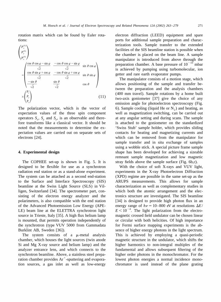
The COPHEE set-up is shown in Fig. 5. It is stray fields above the sample surface (Fig. 6b,c).designed to be flexible for use as a synchrotron With the choice of soft X-rays and VUV light,radiation end station or as a stand-alone experiment. experiments in the X-ray Photoelectron DiffractionThe system can be attached as a second end-station (XPD) regime are possible in the same set-up as theto the Surface and Interface Spectroscopy (SIS) ARUPS measurements. This allows for samplebeamline at the Swiss Light Source (SLS) in Vil- characterization as well as complementary studies inligen, Switzerland [34]. The spectrometer part, con- which both the atomic arrangement and the elec-sisting of the electron energy analyzer and the tronics structure are investigated. The SIS beamlinepolarimeters, is also compatible with the end station [34] is designed to provide high photon flux in anof the Advanced Photoemission Low Energy (APE- energy range of hn 5 10–800 eV at resolutions DE /
24LE) beam line at the ELETTRA synchrotron light E , 10 . The light polarization from the electro-source in Trieste, Italy [35]. A high flux helium lamp magnetic crossed field undulator can be chosen linearis mounted, that permits operation independently of or circular with both helicities. Of high importancethe synchrotron (type VUV 5000 from Gammadata for Fermi surface mapping experiments is the ab-Burklint AB, Sweden [36]). sence of higher energy photons in the light spectrum.
The system consists of a m-metal analysis This is achieved by employing a quasi-periodicchamber, which houses the light sources (twin anode magnetic structure in the undulator, which shifts theSi and Mg X-ray source and helium lamp) and the higher harmonics to non-integral multiples of theanalyzer entrance lens, and which connects to the fundamental and allows subsequent filtering of thesynchrotron beamline. Above, a stainless steel prepa- higher order photons in the monochromator. For the
1ration chamber provides Ar -sputtering and evapora- lowest photon energies a normal incidence mono-tion sources, a gas inlet as well as low-energy chromator is used instead of the plane grating
272 M. Hoesch et al. / Journal of Electron Spectroscopy and Related Phenomena 124 (2002) 263 –279
Fig. 5. Drawing of the COPHEE set-up consisting of the analysis and preparation chambers with the sample manipulator and the analyzerand polarimeters as well as a pump tube.
monochromator, providing additional filtering of integrated measurements and an accelerating extrac-parasitic higher energy light. tion lens for transport of the photoelectrons into the
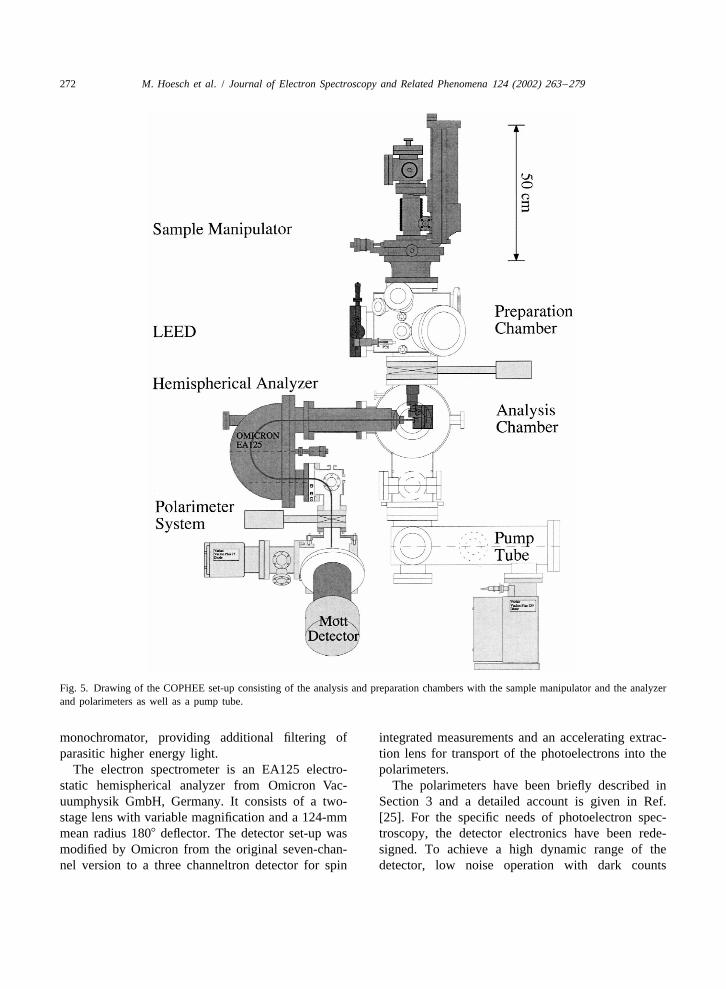
The electron spectrometer is an EA125 electro- polarimeters.static hemispherical analyzer from Omicron Vac- The polarimeters have been briefly described inuumphysik GmbH, Germany. It consists of a two- Section 3 and a detailed account is given in Ref.stage lens with variable magnification and a 124-mm [25]. For the specific needs of photoelectron spec-mean radius 1808 deflector. The detector set-up was troscopy, the detector electronics have been rede-modified by Omicron from the original seven-chan- signed. To achieve a high dynamic range of thenel version to a three channeltron detector for spin detector, low noise operation with dark counts
M. Hoesch et al. / Journal of Electron Spectroscopy and Related Phenomena 124 (2002) 263 –279 273
limited only by cosmic background radiation must bepossible. At the same time the maximum count rateis rather moderate due to the high resolution of theenergy and angular filters and the low reflectivity ofthe gold foil. The pre-amplifier was completely re-designed with an increased shaping time and theoriginal Silicon Surface Barrier (SSB) sensors werereplaced by diodes manufactured by the PassivatedImplanted Planar Silicon (PIPS) process.
The largest task in realizing COPHEE, which wedescribe in more detail here, was the design of atransport electron optical system including a two-way switch to inject the electrons coming from theanalyzer into the Mott detectors. The requirementsare: (i) a chromatic range of a decade if the opticsare to be used in identical mode at analyzer passenergies from 1 to 10 eV; (ii) a high transmissionclose to 100% to prevent further loss of signal in thisflux-hungry experiment; (iii) space constraints due tothe different chambers to which the system must becompatible and the large size of the Mott detectorsand the necessity of a vacuum valve to separate theMott detectors, containing the sensitive gold foils,from the main chamber during sample preparationand maintenance.
(i) Any electron optical system behaves identicalat different kinetic energies if all electrode voltagesare scaled proportional to the energy. In our case, therelevant energy is the analyzer pass energy and thereference potential for the voltages is the Herzogplate of the analyzer. The extraction lens made byOmicron is designed to form a narrow beam withsmall angular spread if a total acceleration to 300times the pass energy is used. This means that the
9kinetic energy in the beam transport system is E 5P
300–3000 eV if a pass energy range of E 5 1–10 eVP
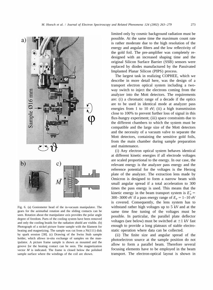
is covered. Consequently, the lens system has toFig. 6. (a) Goniometer head of the in-vacuum manipulator. The withstand rather high voltages up to 5 kV and at thegears for the azimuthal rotation and the sliding contacts can be same time fine tuning of the voltages must beseen. Rotation about the manipulator axis provides the polar angle possible. In particular, the parallel plate deflectordegree of freedom. Parts of the cooling system have been removed
voltages (see below) must be switched at 61 kV fastand only the cooling braids for the radiation shield are visible. (b)enough to provide a long plateaux of stable electro-Photograph of a nickel picture frame sample with the filament for
heating and magnetizing. The sample was cut from a Ni(111) disk static operation where data can be collected.by spark erosion [38]. (c) Drawing of the Swiss Stub sample (ii) The finite size and angular spread of theholder, which allows in-situ exchange of samples on the man- photoelectron source at the sample position do notipulator. A picture frame sample is shown as mounted and the
allow to form a parallel beam. Therefore severalgroove for the heating contact can be seen. The magnetization→ focusing elements have to be employed in the beamvector M is indicated. The frame is closed below the polishedsample surface where the windings of the coil are shown. transport. The electron-optical layout is shown in
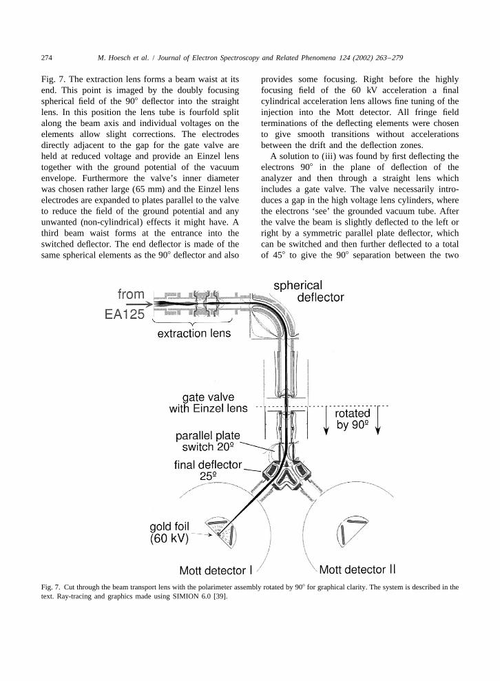
274 M. Hoesch et al. / Journal of Electron Spectroscopy and Related Phenomena 124 (2002) 263 –279
Fig. 7. The extraction lens forms a beam waist at its provides some focusing. Right before the highlyend. This point is imaged by the doubly focusing focusing field of the 60 kV acceleration a finalspherical field of the 908 deflector into the straight cylindrical acceleration lens allows fine tuning of thelens. In this position the lens tube is fourfold split injection into the Mott detector. All fringe fieldalong the beam axis and individual voltages on the terminations of the deflecting elements were chosenelements allow slight corrections. The electrodes to give smooth transitions without accelerationsdirectly adjacent to the gap for the gate valve are between the drift and the deflection zones.held at reduced voltage and provide an Einzel lens A solution to (iii) was found by first deflecting thetogether with the ground potential of the vacuum electrons 908 in the plane of deflection of theenvelope. Furthermore the valve’s inner diameter analyzer and then through a straight lens whichwas chosen rather large (65 mm) and the Einzel lens includes a gate valve. The valve necessarily intro-electrodes are expanded to plates parallel to the valve duces a gap in the high voltage lens cylinders, whereto reduce the field of the ground potential and any the electrons ‘see’ the grounded vacuum tube. Afterunwanted (non-cylindrical) effects it might have. A the valve the beam is slightly deflected to the left orthird beam waist forms at the entrance into the right by a symmetric parallel plate deflector, whichswitched deflector. The end deflector is made of the can be switched and then further deflected to a totalsame spherical elements as the 908 deflector and also of 458 to give the 908 separation between the two
Fig. 7. Cut through the beam transport lens with the polarimeter assembly rotated by 908 for graphical clarity. The system is described in thetext. Ray-tracing and graphics made using SIMION 6.0 [39].
M. Hoesch et al. / Journal of Electron Spectroscopy and Related Phenomena 124 (2002) 263 –279 275
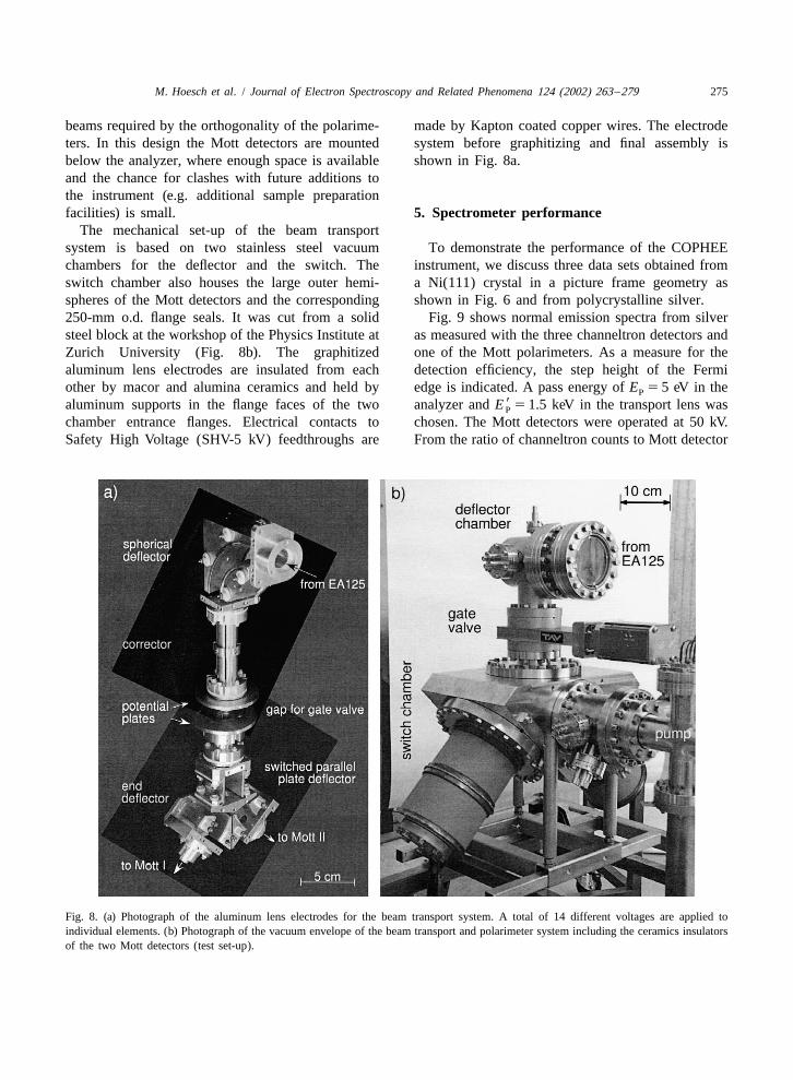
beams required by the orthogonality of the polarime- made by Kapton coated copper wires. The electrodeters. In this design the Mott detectors are mounted system before graphitizing and final assembly isbelow the analyzer, where enough space is available shown in Fig. 8a.and the chance for clashes with future additions tothe instrument (e.g. additional sample preparationfacilities) is small. 5. Spectrometer performance
The mechanical set-up of the beam transportsystem is based on two stainless steel vacuum To demonstrate the performance of the COPHEEchambers for the deflector and the switch. The instrument, we discuss three data sets obtained fromswitch chamber also houses the large outer hemi- a Ni(111) crystal in a picture frame geometry asspheres of the Mott detectors and the corresponding shown in Fig. 6 and from polycrystalline silver.250-mm o.d. flange seals. It was cut from a solid Fig. 9 shows normal emission spectra from silversteel block at the workshop of the Physics Institute at as measured with the three channeltron detectors andZurich University (Fig. 8b). The graphitized one of the Mott polarimeters. As a measure for thealuminum lens electrodes are insulated from each detection efficiency, the step height of the Fermiother by macor and alumina ceramics and held by edge is indicated. A pass energy of E 5 5 eV in theP
9aluminum supports in the flange faces of the two analyzer and E 5 1.5 keV in the transport lens wasP
chamber entrance flanges. Electrical contacts to chosen. The Mott detectors were operated at 50 kV.Safety High Voltage (SHV-5 kV) feedthroughs are From the ratio of channeltron counts to Mott detector
Fig. 8. (a) Photograph of the aluminum lens electrodes for the beam transport system. A total of 14 different voltages are applied toindividual elements. (b) Photograph of the vacuum envelope of the beam transport and polarimeter system including the ceramics insulatorsof the two Mott detectors (test set-up).
276 M. Hoesch et al. / Journal of Electron Spectroscopy and Related Phenomena 124 (2002) 263 –279
compromise between magnetizing current and sam-ple heating.
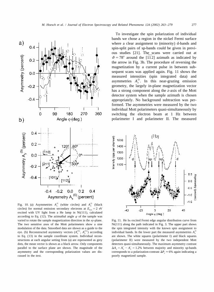
To determine the direction of magnetization, sec-ondary electrons excited with UV light from the Helamp were measured in normal emission. Fig. 10ashows the measured asymmetries A (polarimeter II)x
and A (polarimeter I) as a function of the azimuthaly
angle w of the sample, which determines the match-ing of the magnetization direction with the sensitiveaxes of the polarimeters in this normal-emissiongeometry. To eliminate instrumental asymmetries,the measurements were performed after magnetizingthe sample with current pulses of both polarities, andthe cross-asymmetries were calculated as
% * % *(N 1 N ) 2 (N 1 N )L R R L^ ]]]]]]]A 5 (12)% * % *(N 1 N ) 1 (N 1 N )L R R L
% *where N and N denote measurements with therespective magnetization polarities and L, R have tobe replaced by the appropriate channels as shown in
^Eq. (10). The statistical error of A can be calculatedanalogous to Eq. (9). From these data the in-planecomponent of the magnetization vector in the samplecoordinates was reconstructed according to Eq. (11)as
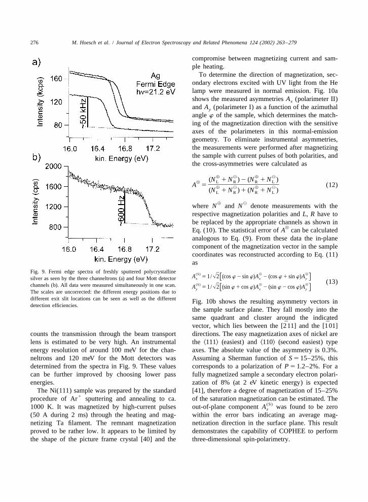
Fig. 9. Fermi edge spectra of freshly sputtered polycrystalline ](S) ^ ^ŒA 5 1/ 2 (cos w 2 sin w)A 2 (cos w 1 sin w)Af gx x ysilver as seen by the three channeltrons (a) and four Mott detector (13)](S) ^ ^channels (b). All data were measured simultaneously in one scan. ŒA 5 1/ 2 (sin w 1 cos w)A 2 (sin w 2 cos w)Af gy x yThe scales are uncorrected: the different energy positions due todifferent exit slit locations can be seen as well as the different Fig. 10b shows the resulting asymmetry vectors indetection efficiencies.
the sample surface plane. They fall mostly into thesame quadrant and cluster around the indicated
¯ ¯vector, which lies between the [211] and the [101]counts the transmission through the beam transport directions. The easy magnetization axes of nickel arelens is estimated to be very high. An instrumental the k111l (easiest) and k110l (second easiest) typeenergy resolution of around 100 meV for the chan- axes. The absolute value of the asymmetry is 0.3%.neltrons and 120 meV for the Mott detectors was Assuming a Sherman function of S 5 15–25%, thisdetermined from the spectra in Fig. 9. These values corresponds to a polarization of P 5 1.2–2%. For acan be further improved by choosing lower pass fully magnetized sample a secondary electron polari-energies. zation of 8% (at 2 eV kinetic energy) is expected
The Ni(111) sample was prepared by the standard [41], therefore a degree of magnetization of 15–25%1procedure of Ar sputtering and annealing to ca. of the saturation magnetization can be estimated. The
(S)1000 K. It was magnetized by high-current pulses out-of-plane component A was found to be zeroz
(50 A during 2 ms) through the heating and mag- within the error bars indicating an average mag-netizing Ta filament. The remnant magnetization netization direction in the surface plane. This resultproved to be rather low. It appears to be limited by demonstrates the capability of COPHEE to performthe shape of the picture frame crystal [40] and the three-dimensional spin-polarimetry.
M. Hoesch et al. / Journal of Electron Spectroscopy and Related Phenomena 124 (2002) 263 –279 277
To investigate the spin polarization of individualbands we chose a region in the nickel Fermi surfacewhere a clear assignment to (minority) d-bands andspin-split pairs of sp-bands could be given in previ-ous studies [21]. The scans were carried out at
¯ ¯q 5 788 around the [112] azimuth as indicated bythe arrow in Fig. 3b. The procedure of reversing themagnetization by a current pulse in between sub-sequent scans was applied again. Fig. 11 shows themeasured intensities (spin integrated data) and
^asymmetries A . In this near-grazing emissionz
geometry, the largely in-plane magnetization vectorhas a strong component along the z-axis of the Mottdetector system when the sample azimuth is chosenappropriately. No background subtraction was per-formed. The asymmetries were measured by the twoindividual Mott polarimeters quasi-simultaneously byswitching the electron beam at 1 Hz betweenpolarimeter I and polarimeter II. The measured
^ ^Fig. 10. (a) Asymmetries A (white circles) and A (blackx y
circles) for normal emission secondary electrons at E 5 2 eVkin
excited with UV light from a He lamp in Ni(111), calculatedaccording to Eq. (12). The azimuthal angle w of the sample wasvaried to rotate the sample magnetization direction in the xy-plane. Fig. 11. He Ia excited Fermi edge angular distribution curve fromThe two sensitive axes of the Mott polarimeters show a sine Ni(111) along the path indicated in Fig. 3. The upper part showsmodulation of the data. Smoothed data are shown as a guide to the the spin integrated intensity with the known spin assignment to
(S) (S) ^eye. (b) Reconstructed asymmetry vectors (A , A ) according individual bands. In the lower part the measured asymmetries Ax y z
to Eq. (13) in the sample coordinate system. Individual recon- are shown. The white squares (polarimeter I) and black squaresstructions at each angular setting from (a) are represented as grey (polarimeter II) were measured by the two independent Mottdots, the mean vector is shown as a black arrow. Only components detectors quasi-simultaneously. The maximum asymmetry contrast
↑ ↓parallel to the surface plane are shown. The magnitude of the DA 5 A 2 A 5 1.2% between majority and minority sp-bandsz z z
asymmetry and the corresponding polarization values are dis- corresponds to a polarization-contrast DP . 6% again indicating az
cussed in the text. poorly magnetized sample.
278 M. Hoesch et al. / Journal of Electron Spectroscopy and Related Phenomena 124 (2002) 263 –279
asymmetries were found to be larger than those of In the future the instrument can be used for athe secondary electrons (Fig. 10) indicating a strong variety of investigations. (i) For bulk magneticpolarization of these electrons photoemitted by direct materials the technique of Fermi surface tomographytransitions from the Fermi level. The overall measur- using various photon energies at a synchrotron lighting time for this data set, from which a spin-resolved source allows the mapping of the complete Fermimomentum distribution curve can be obtained, was surface of a material as seen through its surface.2.5 h. Magnetically active regions can therefore be iden-
tified. (ii) Thin films of magnetic materials as well ascombinations of magnetic and non-magnetic layers,
6. Conclusions and outlook and the coupling between different layers, can beinvestigated. Specifically the spin character of the
We have emphasized the necessity to combine electronic states can now be revealed. (iii) Thehigh resolution angle-scanned photoelectron spec- interplay between surface magnetism and adsorbatestroscopy and spin detection for the investigation of can be studied both by monitoring the reaction ofsurface and thin film magnetism. The interplay substrate bands to adsorbed molecules and bybetween magnetic properties and electronic structure measuring induced magnetism in the adsorbate itself.requires a surface sensitive Fermi surface probe with (iv) In addition to the ARUPS regime the instrumentspin resolution. The technique of Fermi surface can also be used for spin-polarized core level studiesmapping by angle resolved photoemission proves in X-ray photoelectron, Auger electron and resonantsuitable for such systems, and the use of Mott photoemission spectroscopies.detectors in conjunction with Fermi surface mappingequipment was discussed. The requirement formeasuring the full spin polarization vector in these Acknowledgementsexperiments is satisfied using two independent,orthogonally mounted Mott detectors. We have de- We wish to thank Drs Iwao Matsuda, Luc Patthey,scribed the conception and the design of this com- Christoph Quitmann and Ralph E. Pixley for manyplete photoemission experiment extensively. First fruitful discussions. Dr Giorgio Rossi first proposedexperiments on Ni(111) show the capability of the the use of two independent Mott detectors. Drsinstrument to measure the polarization as a vector Detlef Vermeulen, Steve Hunt and Markus Janouschquantity and to determine the spin character of of the SLS Computing and Controls group providedelectronic states at the Fermi level. The ultimate hardware and conceptual support for the EPICS-energy and angular resolution of this spin-resolved based data acquisition system. We are greatly in-electron spectrometer is an unprecedented 15 meV debted to the staff of the mechanical workshop of theand 618, respectively and is thus sufficient to Physics Institute in Zurich, in particular to B.address many of the problems discussed in the Schmid, P. Treier and B. Wachter and to the groupintroduction. technician W. Deichmann. Financial support from the
The spin resolution can now be used for three Swiss National Science Foundation (REQUIP 21-purposes. First, the sign of the polarization gives 53281.98 in collaboration with D. Pescia, ETHinformation on the spin character of electronic states. Zurich and P. Aebi, University of Fribourg) isSecond, the degree of spin polarization can be gratefully acknowledged.measured and therefore the degree of magnetisationfor individual states can be measured, e.g. in tem-perature-dependent studies. Third, the position and
Referenceswidth of peaks in the polarization signal can be usedfor a more precise determination of binding energies
[1] F.J. Himpsel, J.E. Ortega, G.J. Mankey, R.F. Willis, Adv.and momenta and it can even resolve spectral Phys. 47 (1998) 511.features that might not be visible in spin integrated [2] G.A. Prinz, Science 282 (1998) 1660;spectroscopies. S.A. Wolf, D.D. Awschalom, R.A. Buhrman, J.M. Daughton,
M. Hoesch et al. / Journal of Electron Spectroscopy and Related Phenomena 124 (2002) 263 –279 279
´S. von Molnar, M.L. Roukes, A.Y. Chtchelkanova, D.M. N.F. Mott, Proc. R. Soc. Lond., Ser. A 135 (1932) 429.Treger, Science 294 (2001) 1488. [23] N. Sherman, Phys. Rev. 103 (1956) 1601.
[3] J.E. Ortega, F.J. Himpsel, Phys. Rev. Lett. 69 (1992) 844. [24] J. Kessler, Polarized Electrons, 2nd Edition, Springer, Berlin,[4] B.G. Briner et al., Europhys. News 28 (1997) 149. 1985.[5] R.H. Gaylord, K. Jeong, S.D. Kevan, Phys. Rev. Lett. 62 [25] V.N. Petrov, M. Landolt, M.S. Galaktionov, B.V. Yushenkov,
(1989) 203. Rev. Sci. Instrum. 68 (1997) 4385.[6] A. Santoni, L.J. Terminello, F.J. Himpsel, T. Takahashi, [26] V.N. Petrov, M.S. Galaktionov, A.S. Kamochkin, Rev. Sci.
Appl. Phys. A52 (1991) 229. Instrum. 72 (2001) 3729.[7] P. Aebi, J. Osterwalder, R. Fasel, D. Naumovic, L. Schlap- [27] M. Landolt, D. Mauri, Phys. Rev. Lett. 49 (1982) 1783.
bach, Surf. Sci. 307–309 (1994) 917. [28] S. Qiao, A. Kimura, A. Harasawa, M. Sawada, J.-G. Chung,[8] J. Osterwalder, Surf. Rev. Lett. 4 (1997) 391. A. Kakizaki, Rev. Sci. Instrum. 68 (1997) 4390.[9] P. Aebi, T.J. Kreutz, J. Osterwalder, R. Fasel, P. Schwaller, [29] L.G. Gray, M.W. Hart, F.B. Dunning, G.K. Walters, Rev. Sci.
L. Schlapbach, Phys. Rev. Lett. 76 (1996) 1150. Instrum. 55 (1984) 88.[10] T. Greber, T.J. Kreutz, J. Osterwalder, Phys. Rev. Lett. 79 [30] S. Qiao, A. Kakizaki, Rev. Sci. Instrum. 68 (1997) 4017.
(1997) 4465. [31] G.C. Burnett, T.J. Monroe, F.B. Dunning, Rev. Sci. Instrum.[11] H.C. Siegmann, F. Meier, M. Erbudak, M. Landolt, Adv. 65 (1994) 1893.
Electron. Electron Phys. 62 (1984) 1, and references therein. [32] J. Kirschner, Polarized Electrons at Surfaces, Springer,¨ ¨[12] K.-P. Kampfer, W. Schmitt, G. Guntherodt, Phys. Rev. B 42 Berlin, 1985.
(1990) 10696. [33] J. Unguris, D.T. Pierce, R.J. Celotta, Rev. Sci. Instrum. 57[13] W.H. Butler, X.-G. Zhang, D.M.C. Nicholson, T.C. Schul- (1986) 1314.
thess, J.M. MacLaren, Phys. Rev. Lett. 76 (1996) 3216. [34] see http: / /www.psi.ch /sls /[14] C.T. Chen, J. Electron Spectrosc. Relat. Phenom. 92 (1998) [35] see http: / /www.elettra.trieste.it /
289. [36] P. Baltzer, L. Karlsson, M. Lundquist, B. Wanneberg, Rev.[15] F. Manghi, V. Bellini, J. Osterwalder, T.J. Kreutz, P. Aebi, C. Sci. Instrum. 64 (1993) 2179.
Arcangeli, Phys. Rev. B 59 (1999) R10409. [37] T. Greber, O. Raetzo, T.J. Kreutz, P. Schwaller, W. Deich-[16] J. Osterwalder, J. Electron Spectrosc. Relat. Phenom. 117– mann, E. Wetli, J. Osterwalder, Rev. Sci. Instrum. 68 (1997)
118 (2001) 71. 4549.[17] P.J. Feibelman, D.E. Eastman, Phys. Rev. B (1974) 104932. [38] The crystal was grown and cut by MaTecK Material-Tech-
¨[18] C.N. Berglund, W.E. Spicer, Phys. Rev. A 136 (1964) 1030 nologie & Kristalle GmbH, 52428 Julich, Germany.and 1044. [39] ‘SIMION 3D Version 6.0’ by David A. Dahl, 43rd ASMS
¨[19] S. Hufner, Photoelectron Spectroscopy, Springer, Berlin, Conference on Mass Spectrometry and Allied Topics, May1995. 21–26 1995, Atlanta, GA, p. 717; http: / /www.srv.net / |
[20] E. Bertel, M. Donath (Eds.), Electronic Surface States and klack /simion.htmlInterface States on Metallic Systems, World Scientific, [40] M. Donath, Surf. Sci. Rep. 20 (1994) 251.Singapore, 1995. [41] M. Landolt, Spin Polarized Secondary Electron Emission
[21] T.J. Kreutz, T. Greber, P. Aebi, J. Osterwalder, Phys. Rev. B from Ferromagnets, in: R. Feder (Ed.), Polarized Electrons in58 (1998) 1300. Surface Science, World Scientific, Singapore, 1985.
[22] N.F. Mott, Proc. R. Soc. Lond., Ser. A 124 (1929) 425;