Embed Size (px)
Citation preview
STUDY OF SOFT SWITCHING BOOST CONVERTER
USING AN AUXILIARY RESONANT CIRCUIT
BISWAJEET PANDA (108EE004)
ASHIRBAD SAHOO (108EE016)
Department of Electrical Engineering
National Institute of Technology Rourkela
- 2 -
STUDY OF SOFT SWITCHING BOOST CONVERTER
USING AN AUXILIARY RESONANT CIRCUIT
A Thesis submitted in partial fulfillment of the requirements for the degree of
Bachelor of Technology in “Electrical Engineering”
By
BISWAJEET PANDA (108EE004)
ASHIRBAD SAHOO (108EE016)
Department of Electrical Engineering
National Institute of Technology
Rourkela-769008 (ODISHA)
May-2012
- 3 -
STUDY OF SOFT SWITCHING BOOST CONVERTER
USING AN AUXILIARY RESONANT CIRCUIT
A Thesis submitted in partial fulfillment of the requirements for the degree of
Bachelor of Technology in “Electrical Engineering”
By
BISWAJEET PANDA (108EE004)
ASHIRBAD SAHOO (108EE016)
Under guidance of
Prof. B.CHITTI BABU
Department of Electrical Engineering
National Institute of Technology
Rourkela-769008 (ODISHA)
May-2012
- 4 -
DEPARTMENT OF ELECTRICAL ENGINEERING
NATIONAL INSTITUTE OF TECHNOLOGY, ROURKELA
ODISHA, INDIA-769008
CERTIFICATE
This is to certify that the thesis entitled “Study of Soft Switching Boost Converter
using an Auxiliary Resonant Circuit ”, submitted by Biswajeet Panda(Roll. No.
108EE004) and Ashirbad Sahoo(Roll. No. 108EE016) in partial fulfilment of the requirements
for the award of Bachelor of Technology in Electrical Engineering during session 2011-2012
at National Institute of Technology, Rourkela. A bonafide record of research work carried out by
them under my supervision and guidance.
The candidates have fulfilled all the prescribed requirements.
The Thesis which is based on candidates’ own work, have not submitted elsewhere for a
degree/diploma.
In my opinion, the thesis is of standard required for the award of a bachelor of technology degree
in Electrical Engineering.
Place: Rourkela
Dept. of Electrical Engineering Prof. B.Chitti Babu
National institute of Technology Assistant Professor
Rourkela-769008
a
ACKNOWLEDGEMENTS
On the submission of our thesis entitled “Study of Soft Switching Boost Converter using an
Auxiliary Resonant Circuit”, we would like to extend our gratitude & our sincere thanks to our
supervisor Prof. B.Chitti Babu, Asst. Professor, Department of Electrical Engineering for his
constant motivation and support during the course of our work in the last one year. We truly
appreciate and value his esteemed guidance and encouragement from the beginning to the end of
this thesis. His knowledge and company at the time of crisis would be remembered lifelong.
We are very thankful to our teachers Dr. B.D.Subudhi, Prof. K.B Mohanty and Prof.
A.K.Panda for providing solid background for our studies and research thereafter. They have
great sources of inspiration to us and we thank them from the bottom of our hearts.
At last but not least, we would like to thank the staff of Electrical engineering department for
constant support and providing place to work during project period. We would also like to extend
our gratitude to our friends who are with us during thick and thin.
Biswajeet Panda
Ashirbad Sahoo
B.Tech (Electrical Engineering)

b
Dedicated to
Our beloved parents
i
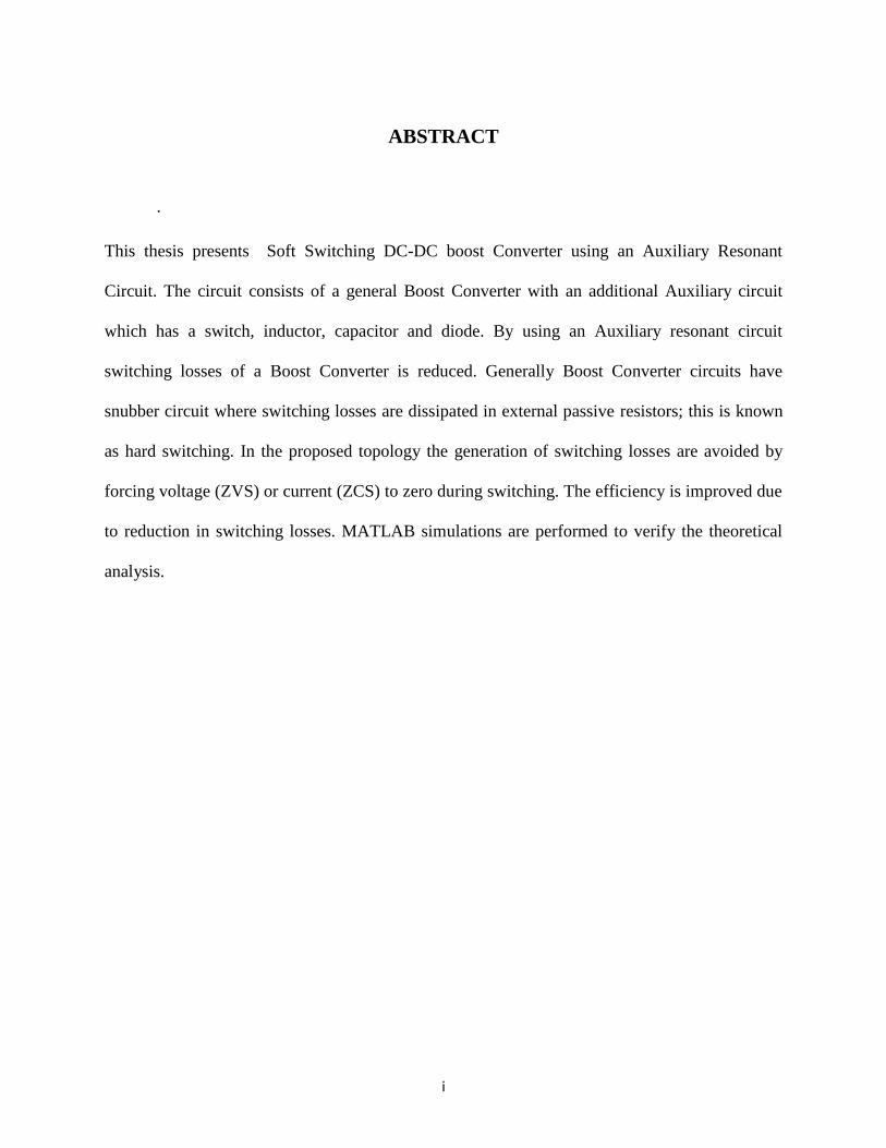
ABSTRACT
.
This thesis presents Soft Switching DC-DC boost Converter using an Auxiliary Resonant
Circuit. The circuit consists of a general Boost Converter with an additional Auxiliary circuit
which has a switch, inductor, capacitor and diode. By using an Auxiliary resonant circuit
switching losses of a Boost Converter is reduced. Generally Boost Converter circuits have
snubber circuit where switching losses are dissipated in external passive resistors; this is known
as hard switching. In the proposed topology the generation of switching losses are avoided by
forcing voltage (ZVS) or current (ZCS) to zero during switching. The efficiency is improved due
to reduction in switching losses. MATLAB simulations are performed to verify the theoretical
analysis.
ii
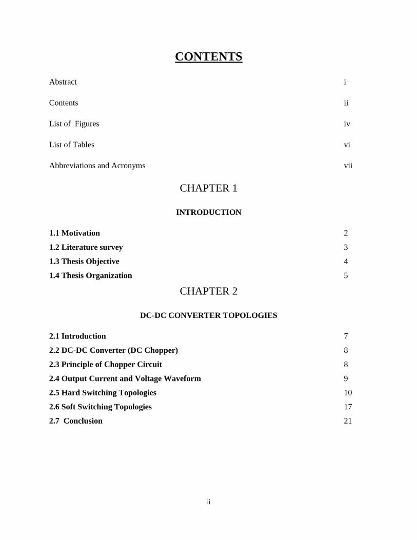
CONTENTS
Abstract i
Contents ii
List of Figures iv
List of Tables vi
Abbreviations and Acronyms vii
CHAPTER 1
INTRODUCTION
1.1 Motivation 2
1.2 Literature survey 3
1.3 Thesis Objective 4
1.4 Thesis Organization 5
CHAPTER 2
DC-DC CONVERTER TOPOLOGIES
2.1 Introduction 7
2.2 DC-DC Converter (DC Chopper) 8
2.3 Principle of Chopper Circuit 8
2.4 Output Current and Voltage Waveform 9
2.5 Hard Switching Topologies 10
2.6 Soft Switching Topologies 17
2.7 Conclusion 21
iii
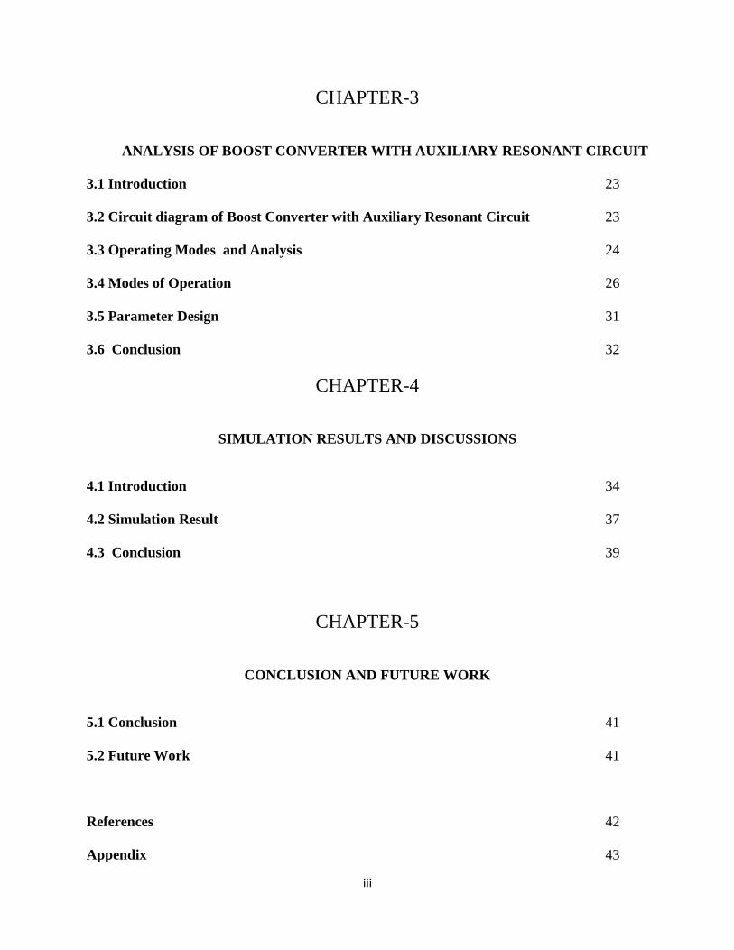
CHAPTER-3
ANALYSIS OF BOOST CONVERTER WITH AUXILIARY RESONANT CIRCUIT
3.1 Introduction 23
3.2 Circuit diagram of Boost Converter with Auxiliary Resonant Circuit 23
3.3 Operating Modes and Analysis 24
3.4 Modes of Operation 26
3.5 Parameter Design 31
3.6 Conclusion 32
CHAPTER-4
SIMULATION RESULTS AND DISCUSSIONS
4.1 Introduction 34
4.2 Simulation Result 37
4.3 Conclusion 39
CHAPTER-5
CONCLUSION AND FUTURE WORK
5.1 Conclusion 41
5.2 Future Work 41
References 42
Appendix 43
iv
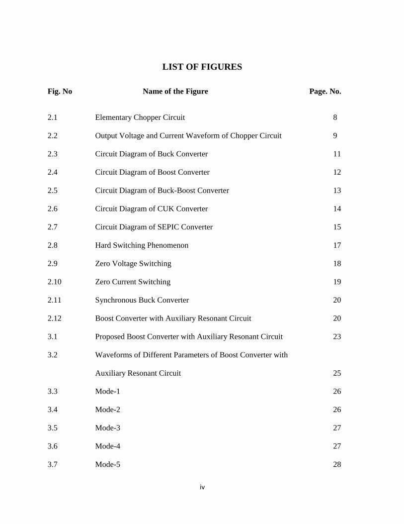
LIST OF FIGURES
Fig. No Name of the Figure Page. No.
2.1 Elementary Chopper Circuit 8
2.2 Output Voltage and Current Waveform of Chopper Circuit 9
2.3 Circuit Diagram of Buck Converter 11
2.4 Circuit Diagram of Boost Converter 12
2.5 Circuit Diagram of Buck-Boost Converter 13
2.6 Circuit Diagram of CUK Converter 14
2.7 Circuit Diagram of SEPIC Converter 15
2.8 Hard Switching Phenomenon 17
2.9 Zero Voltage Switching 18
2.10 Zero Current Switching 19
2.11 Synchronous Buck Converter 20
2.12 Boost Converter with Auxiliary Resonant Circuit 20
3.1 Proposed Boost Converter with Auxiliary Resonant Circuit 23
3.2 Waveforms of Different Parameters of Boost Converter with
Auxiliary Resonant Circuit 25
3.3 Mode-1 26
3.4 Mode-2 26
3.5 Mode-3 27
3.6 Mode-4 27
3.7 Mode-5 28
v
3.8 Mode-6 29
3.9 Mode-7 29
3.10 Mode-8 30
3.11 Mode-9 31
4.1 Circuit Diagram Boost Converter with Auxiliary Resonant Circuit 34
4.2 Overall MATLAB-SIMULINK Model 35
4.3 Gate Pulse Input to Main and Auxiliary Switch 36
4.4 Block Diagram of PWM Generator 37
4.5 Output Voltage Vs Time 37
4.6 Output Current Vs Time 38
4.7 Main Switch Voltage and Current Vs Time Showing ZVS 38
4.8 Auxiliary Switch Voltage and Current Vs Time Showing ZCS 39

vi
LIST OF TABLES
Table. No. Name of the Table Page. No.
2.1 Hard Switching DC-DC Converter Topologies 16
vii
ABBREVIATIONS AND ACRONYMS
PVA - Photo Voltaic Array
AC - Alternating Current
DC - Direct Current
SPV - Solar Photo Voltaic
MOSFET - Metal Oxide Semiconductor Field Effect Transistor
SEPIC - Single Ended Primary Inductor Converter
PWM - Pulse Width Modulation
EMI - Electro Magnetic Interference
ZVS - Zero Voltage Switching
ZCS - Zero Current Switching
ZVT - Zero Voltage Transition
ZCT - Zero Current Transition
MATLAB - MATrix LABoratory
IC - Integrated Circuit

1
CHAPTER 1
INTRODUCTION
2
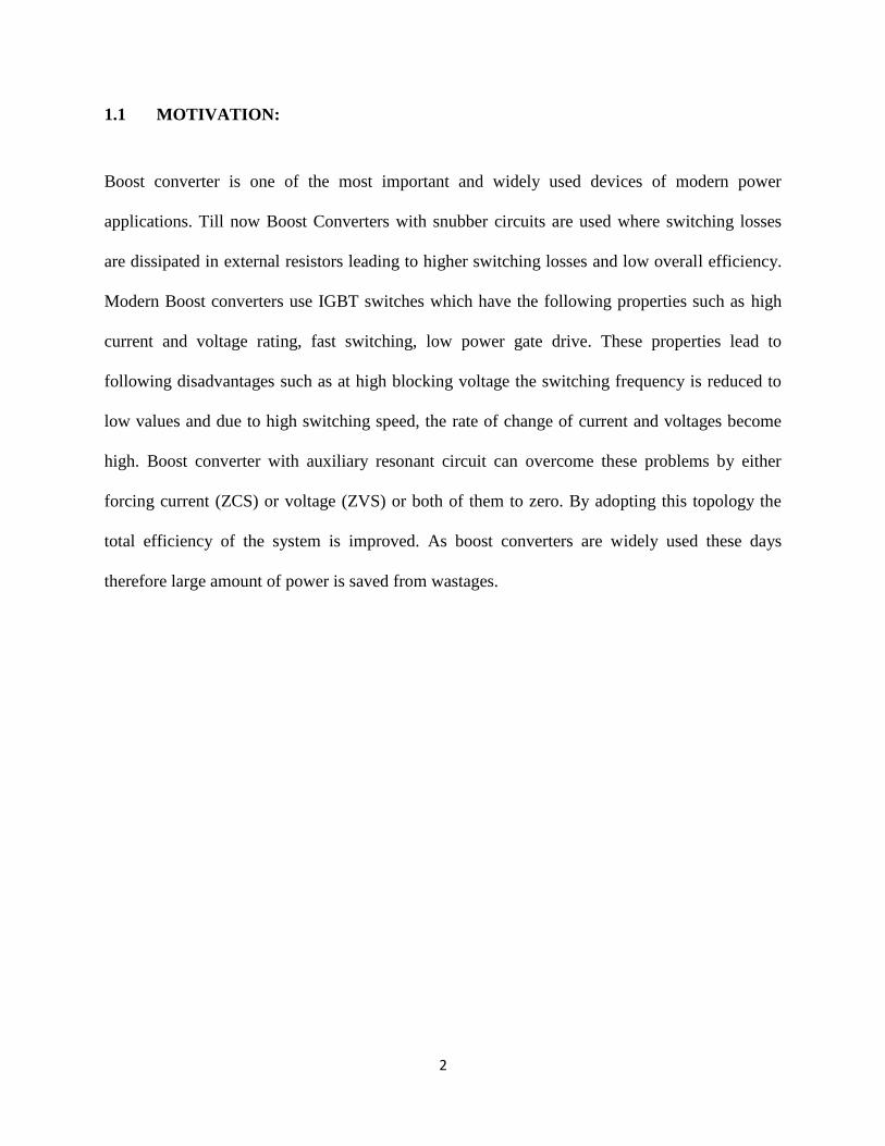
1.1 MOTIVATION:
Boost converter is one of the most important and widely used devices of modern power
applications. Till now Boost Converters with snubber circuits are used where switching losses
are dissipated in external resistors leading to higher switching losses and low overall efficiency.
Modern Boost converters use IGBT switches which have the following properties such as high
current and voltage rating, fast switching, low power gate drive. These properties lead to
following disadvantages such as at high blocking voltage the switching frequency is reduced to
low values and due to high switching speed, the rate of change of current and voltages become
high. Boost converter with auxiliary resonant circuit can overcome these problems by either
forcing current (ZCS) or voltage (ZVS) or both of them to zero. By adopting this topology the
total efficiency of the system is improved. As boost converters are widely used these days
therefore large amount of power is saved from wastages.
3
1.2 LITERATURE SURVEY:
Many previous work has been used to carry out the project which includes notes on converter
simulation and design. Reference [1] gives an overview of Soft Switching Boost Converter with
auxiliary resonant circuit. In this paper simple auxiliary resonant circuit (SARC) is proposed for
soft switching. To reduce the switching losses zero current switching and zero voltage switching
are adopted. Reference [2] proposes soft switching boost converter with H-I bridge auxiliary
resonant circuit. Compared to conventional hard switching boost converter this circuit has better
efficiency of about 96%. The efficiency is improved by reducing switching losses by techniques
given in references [1] to [9].
Due to large overlapping area of voltage and current in hard switching the switching
losses are more. The switching losses are proportional to switching frequency hence higher
switching frequencies are not used. By adopting zero voltage switching (ZVS) and zero current
switching (ZCS) switching frequency is increased and switching losses are minimized.
References [1] to [5] verify the above concepts. Operations with wide range of load and duty
cycle can’t be performed by above techniques hence zero voltage transition and zero current
transition techniques are adopted. These are given in [5] to [8]. Zero current transition (ZCT) and
Zero voltage transition guarantees soft switching with minimum switching losses.
4
1.3 THESIS OBJECTIVES:
The following objectives are hopefully to be achieved at the end of the project.
1) To study the different Soft Switching Converter topologies and how the switching losses
are minimised in comparison to Hard Switching Converters.
2) To study the proposed Soft switching Boost Converter using Auxiliary resonant circuit
and design the parameters of the proposed converter.
3) To simulate the Soft Switching Boost Converter in MATLAB and observe the output
current and voltage waveform, the switching current and voltage waveform of main and
auxiliary switch and compare with theoretical analysis.
4) To study the comparison between the conventional DC-DC Boost converter and the
proposed soft switching DC-DC boost converter using auxiliary resonant circuit in terms
of efficiency improvement and switching loss reduction.
5) To study the 250mV input Boost converter for low power application. To simulate it in
MATLAB and observe the output current and voltage waveform.
5
1.4 THESIS ORGANISATION:
The Proposed thesis is divided into five chapters including the introduction chapter. Each chapter
is different from the other and has its own unique description for better understanding.
Chapter 2: It describes about the different DC-DC converter topologies. The hard
switching converter topologies described in this chapter are Buck converter, Boost converter,
Buck-Boost converter, Ćuk Converter, SEPIC converter. The soft switching converter ,its
concepts and types which includes zero voltage switching (ZVS) and zero current switching
(ZCS).The different soft switching converter topologies.
Chapter 3: It describes the analysis of zero voltage switching (ZVS) Boost converter
and its schematic diagram. The theoretical waveforms and mode of operations.
Chapter 4: It contains the MATLAB simulation of the proposed soft switching Boost
converter with auxiliary resonant circuit. It shows the zero voltage switching (ZVS) and the zero
current switching (ZCS). The required waveforms are obtained and analysed.
Chapter 5: It concludes the work done under this project. The future work that can be
done under this project to improve the efficiency further is also discussed. The future work that
can be undertaken is discussed.

6
CHAPTER 2
DC-DC CONVERTER
TOPOLOGIES
7
2.1 INTRODUCTION:
A power electronic system consists of one or more power electronic converters. A power
electronic converter is made up of power semiconductor devices controlled by integrated
circuits. The switching characteristics of power semiconductor devices permit a power electronic
converter to shape the input power of one form of power to the other. The static power
converters perform this operation very efficiently. The power electronic converters are classified
into six types as under.
i. Diode rectifiers- It converts AC input voltage to fixed DC voltage. The input voltage may
be single phase or three phase.
ii. AC-DC converter (Phase controlled Rectifiers)- It converts constant AC voltage to
variable DC output voltage. The phase controlled converter may be fed from single phase
or three phase source.
iii. DC-DC converters (DC choppers)- A DC chopper converters a fixed D voltage to a
variable DC output.
iv. DC-AC converters (Inverter)- An inverter converts fixed DC voltage to variable AC
voltage. The output may be variable voltage or variable frequency.
v. AC-AC converters- This converts fixed AC voltage to variable AC output voltage. These
are of two types. (1) AC voltage controllers- These converter converts fixed AC voltage
directly to a variable AC voltage at same frequency.(2) Cycloconverters- This circuit
converters input power at one frequency to output power at a different frequency through
one stage conversion.
vi. Static switches- A power semiconductor devices can operate as switches or contactors. It
possesses many advantages over mechanical and electromechanically circuit breakers.
8
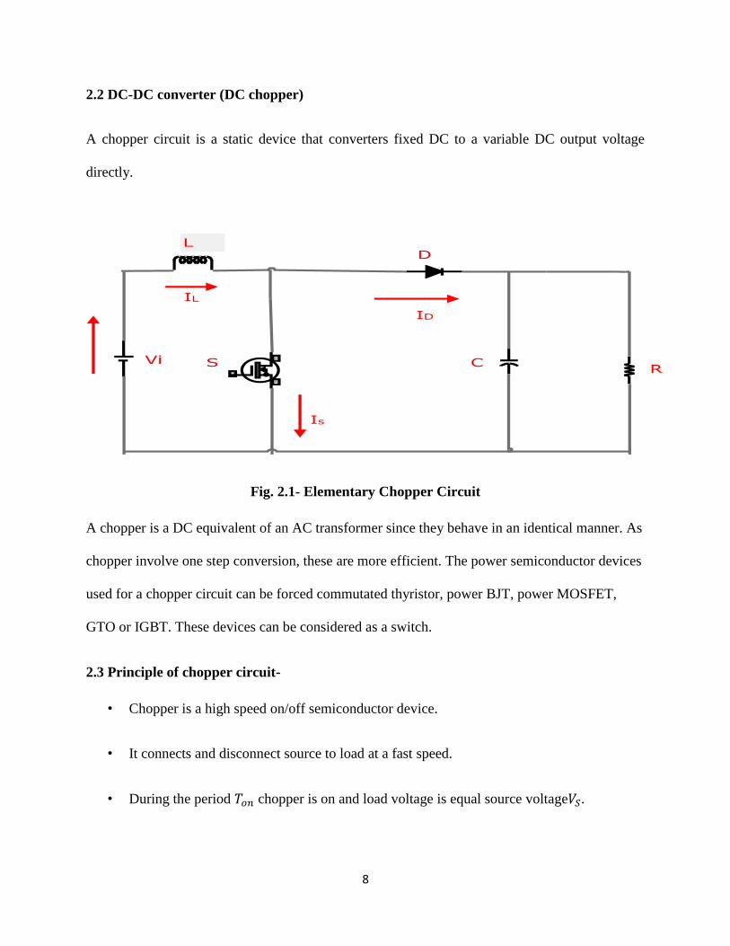
2.2 DC-DC converter (DC chopper)
A chopper circuit is a static device that converters fixed DC to a variable DC output voltage
directly.
Fig. 2.1- Elementary Chopper Circuit
A chopper is a DC equivalent of an AC transformer since they behave in an identical manner. As
chopper involve one step conversion, these are more efficient. The power semiconductor devices
used for a chopper circuit can be forced commutated thyristor, power BJT, power MOSFET,
GTO or IGBT. These devices can be considered as a switch.
2.3 Principle of chopper circuit-
• Chopper is a high speed on/off semiconductor device.
• It connects and disconnect source to load at a fast speed.
• During the period chopper is on and load voltage is equal source voltage .
9
• During the period chopper is off and load current flows through the freewheeling
diode D. As a result load terminals are short circuited by D.And load voltage is therefore
Zero during .
2.4 Output voltage and current waveform
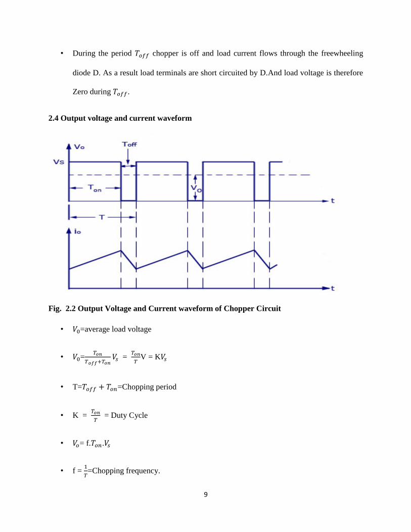
Fig. 2.2 Output Voltage and Current waveform of Chopper Circuit
• =average load voltage
• =
=
V = K
• T= =Chopping period
• K =
= Duty Cycle
• = f. .
• f =
=Chopping frequency.
10
Thus the output voltage can be varied by varying the Duty cycle.
2.5 Hard switching Topologies
Converters which are based on traditional switching are known as hard switching
converter. During Turn ON period the voltage across the switch tends to increase and the
current tends to decrease, which results in some switching losses. Similarly during turn
OFF period the voltage tends to increase and the current tends to decrease across the
switch. Again it leads to some switching losses.
There are many circuit configurations of these traditional hard switching
configurations. They are discussed below.
i. Buck Converter
ii. Boost Converter
iii. Buck – Boost Converter
iv. Ćuk Converter
v. SEPIC Converter
11
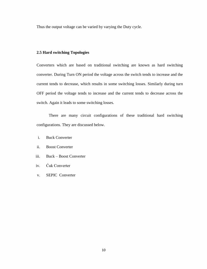
i. Buck Converter
Fig. 2.3 Circuit Diagram of Buck Converter
In Step down converter or Buck converter, the average output voltage Vo is less than the input
voltage Vs. when the switch in turned ON, the voltage across the load is Vs. the current flows
through the circuit as shown in the figure. When the switch is turned OFF, the current direction
is same as before, but the voltage across the load is zero. The power flows from source to load,
hence the output voltage is less than the source voltage, which can be determined by the duty
cycle of the GATE pulse to the switch. The load current is smoothen by the inductor and the
capacitor makes the output voltage ripple free. Hence a constant output voltage is obtained.
12
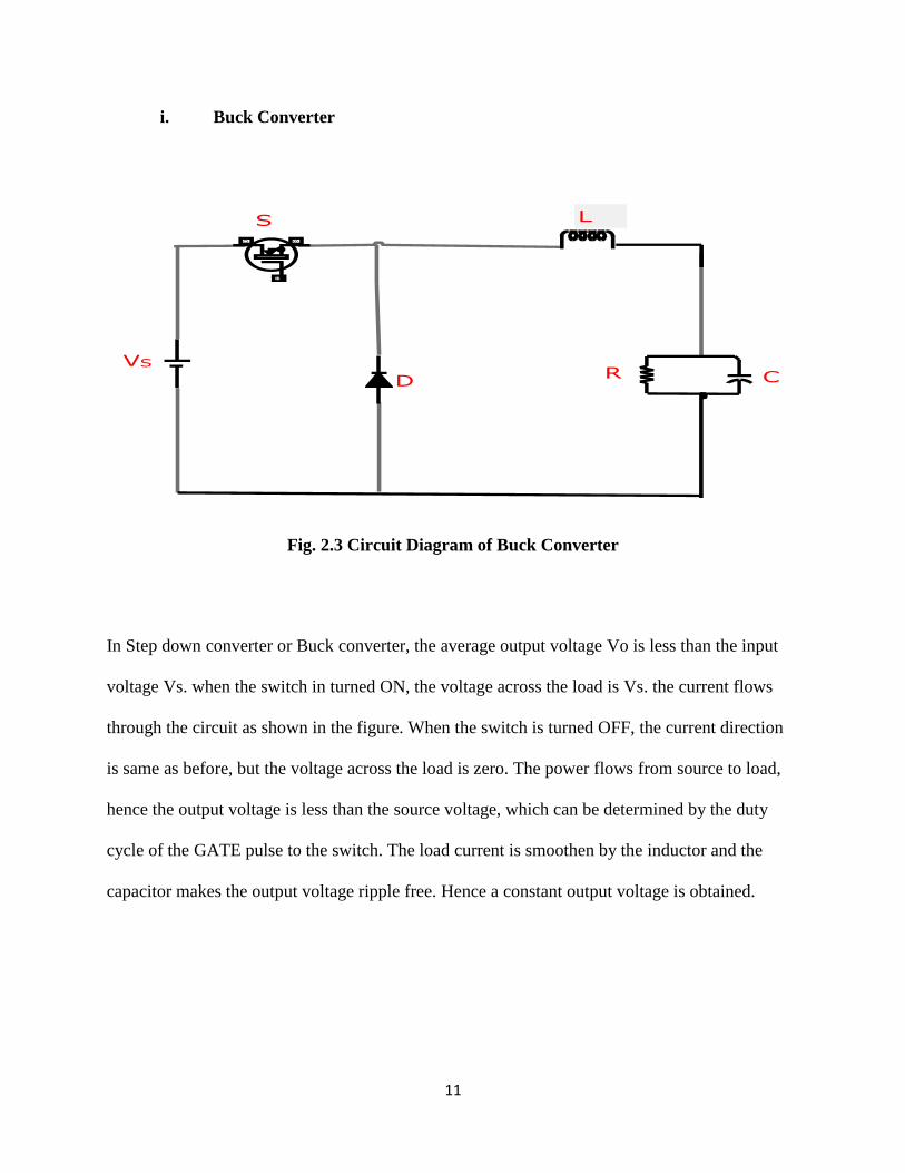
ii. Boost Converter
Fig. 2.4 Circuit Diagram of Boost Converter
In step up converter or Boost converter, the average output voltage Vo is more than the input
voltage Vs. When the switch is turned ON, current through the inductor increases and the
inductor starts to store energy. And when the switch is made OFF, the stored energy in the
inductor starts to dissipate. The current is forced to flow through the Diode and load during the
turn off time. As a result the voltage across the load exceeds the source voltage.
13
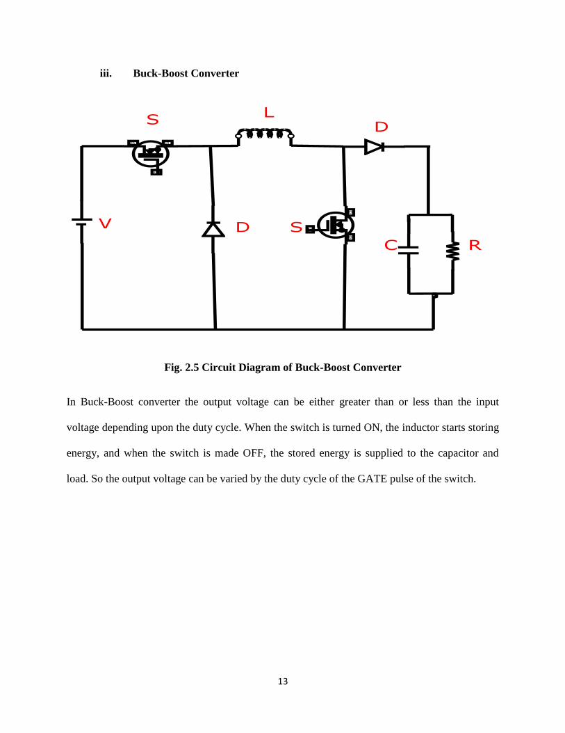
iii. Buck-Boost Converter
Fig. 2.5 Circuit Diagram of Buck-Boost Converter
In Buck-Boost converter the output voltage can be either greater than or less than the input
voltage depending upon the duty cycle. When the switch is turned ON, the inductor starts storing
energy, and when the switch is made OFF, the stored energy is supplied to the capacitor and
load. So the output voltage can be varied by the duty cycle of the GATE pulse of the switch.
14
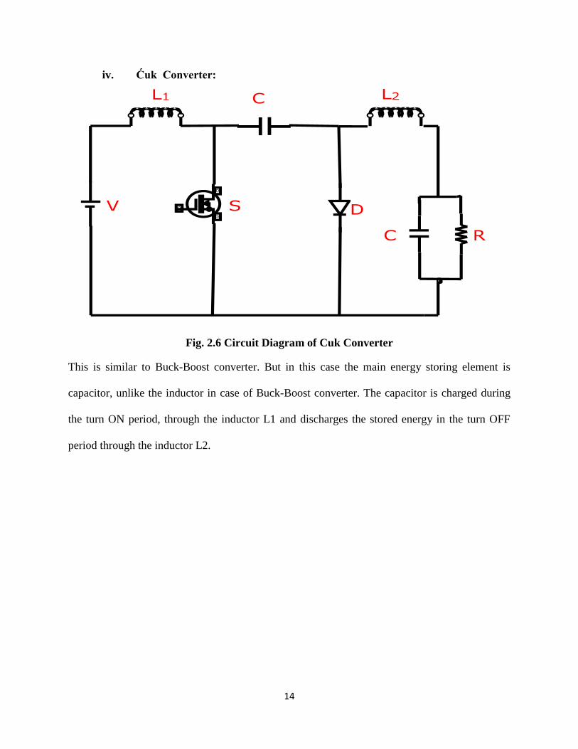
iv. Ćuk Converter:
Fig. 2.6 Circuit Diagram of Cuk Converter
This is similar to Buck-Boost converter. But in this case the main energy storing element is
capacitor, unlike the inductor in case of Buck-Boost converter. The capacitor is charged during
the turn ON period, through the inductor L1 and discharges the stored energy in the turn OFF
period through the inductor L2.
15
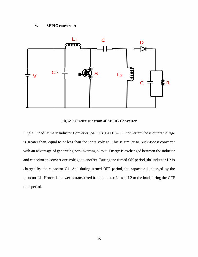
v. SEPIC converter:
Fig.-2.7 Circuit Diagram of SEPIC Converter
Single Ended Primary Inductor Converter (SEPIC) is a DC – DC converter whose output voltage
is greater than, equal to or less than the input voltage. This is similar to Buck-Boost converter
with an advantage of generating non-inverting output. Energy is exchanged between the inductor
and capacitor to convert one voltage to another. During the turned ON period, the inductor L2 is
charged by the capacitor C1. And during turned OFF period, the capacitor is charged by the
inductor L1. Hence the power is transferred from inductor L1 and L2 to the load during the OFF
time period.
16
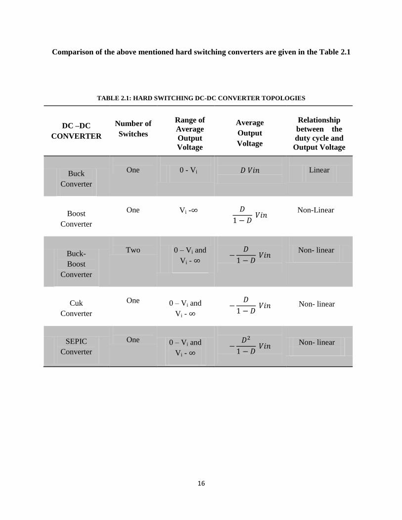
Comparison of the above mentioned hard switching converters are given in the Table 2.1
TABLE 2.1: HARD SWITCHING DC-DC CONVERTER TOPOLOGIES
DC –DC
CONVERTER
Number of
Switches
Range of
Average
Output
Voltage
Average
Output
Voltage
Relationship
between the
duty cycle and
Output Voltage
Buck
Converter
One
0 - Vi
Linear
Boost
Converter
One
Vi -
Non-Linear
Buck-
Boost
Converter
Two
0 – Vi and
Vi -
Non- linear
Cuk
Converter
One
0 – Vi and
Vi -
Non- linear
SEPIC
Converter
One
0 – Vi and
Vi -
Non- linear
17
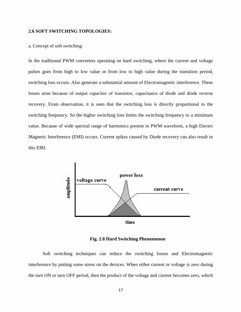
2.6 SOFT SWITCHING TOPOLOGIES:
a. Concept of soft switching:
In the traditional PWM converters operating on hard switching, where the current and voltage
pulses goes from high to low value or from low to high value during the transition period,
switching loss occurs. Also generate a substantial amount of Electromagnetic interference. These
losses arise because of output capacitor of transistor, capacitance of diode and diode reverse
recovery. From observation, it is seen that the switching loss is directly proportional to the
switching frequency. So the higher switching loss limits the switching frequency to a minimum
value. Because of wide spectral range of harmonics present in PWM waveform, a high Electro
Magnetic Interference (EMI) occurs. Current spikes caused by Diode recovery can also result in
this EMI.
Fig. 2.8 Hard Switching Phenomenon
Soft switching techniques can reduce the switching losses and Electromagnetic
interference by putting some stress on the devices. When either current or voltage is zero during
the turn ON or turn OFF period, then the product of the voltage and current becomes zero, which
18
leads to zero power loss. Hence the switching loss can be eliminated and the device can operate
at high switching frequency. Size and weight of the device is reduced as the heat sink is not
required.
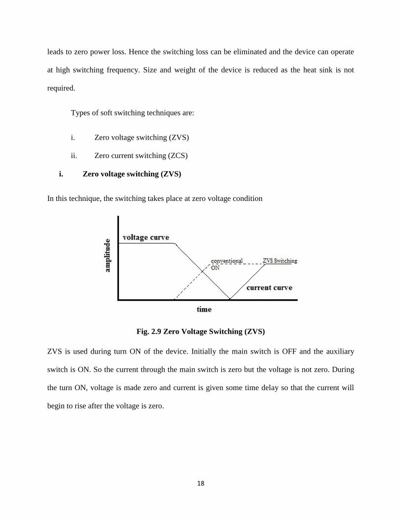
Types of soft switching techniques are:
i. Zero voltage switching (ZVS)
ii. Zero current switching (ZCS)
i. Zero voltage switching (ZVS)
In this technique, the switching takes place at zero voltage condition
Fig. 2.9 Zero Voltage Switching (ZVS)
ZVS is used during turn ON of the device. Initially the main switch is OFF and the auxiliary
switch is ON. So the current through the main switch is zero but the voltage is not zero. During
the turn ON, voltage is made zero and current is given some time delay so that the current will
begin to rise after the voltage is zero.
19
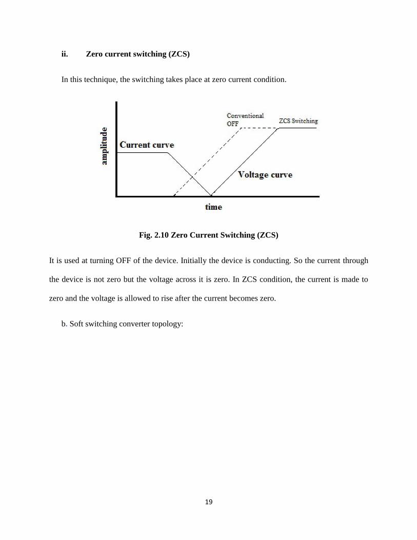
ii. Zero current switching (ZCS)
In this technique, the switching takes place at zero current condition.
Fig. 2.10 Zero Current Switching (ZCS)
It is used at turning OFF of the device. Initially the device is conducting. So the current through
the device is not zero but the voltage across it is zero. In ZCS condition, the current is made to
zero and the voltage is allowed to rise after the current becomes zero.
b. Soft switching converter topology:
20
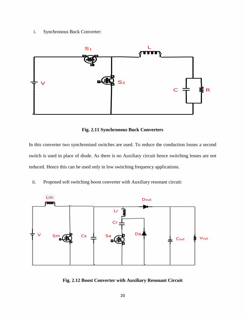
i. Synchronous Buck Converter:
Fig. 2.11 Synchronous Buck Converters
In this converter two synchronised switches are used. To reduce the conduction losses a second
switch is used in place of diode. As there is no Auxiliary circuit hence switching losses are not
reduced. Hence this can be used only in low switching frequency applications.
ii. Proposed soft switching boost converter with Auxiliary resonant circuit:
Fig. 2.12 Boost Converter with Auxiliary Resonant Circuit
21
In the proposed Soft Switching DC-DC boost Converter using an Auxiliary Resonant Circuit.
The circuit consists of a general Boost Converter with an additional Auxiliary circuit which has a
switch, inductor, capacitor and diode. By using an Auxiliary resonant circuit switching losses of
a Boost Converter is reduced. In the proposed topology the generation of switching losses are
avoided by forcing voltage (ZVS) or current (ZCS) to zero during switching.
2.7 CONCLUSION
In this chapter different types of hard switching boost converter topologies are studied which
include buck converter, boost converter, buck-boost converter, cuk converter, SEPIC converter.
Different types of soft switching techniques such as zero voltage switching and zero current
switching are studied. Various soft switching converter topologies such as Synchronous buck
converter and Boost Converter with auxiliary resonant circuit are studied.
22
CHAPTER 3
ANALYSIS OF BOOST
CONVERTER WITH
AUXILIARY RESONANT
CIRCUIT
23
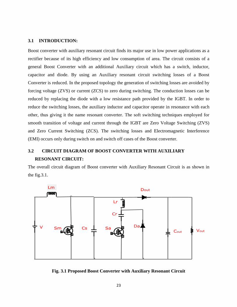
3.1 INTRODUCTION:
Boost converter with auxiliary resonant circuit finds its major use in low power applications as a
rectifier because of its high efficiency and low consumption of area. The circuit consists of a
general Boost Converter with an additional Auxiliary circuit which has a switch, inductor,
capacitor and diode. By using an Auxiliary resonant circuit switching losses of a Boost
Converter is reduced. In the proposed topology the generation of switching losses are avoided by
forcing voltage (ZVS) or current (ZCS) to zero during switching. The conduction losses can be
reduced by replacing the diode with a low resistance path provided by the IGBT. In order to
reduce the switching losses, the auxiliary inductor and capacitor operate in resonance with each
other, thus giving it the name resonant converter. The soft switching techniques employed for
smooth transition of voltage and current through the IGBT are Zero Voltage Switching (ZVS)
and Zero Current Switching (ZCS). The switching losses and Electromagnetic Interference
(EMI) occurs only during switch on and switch off cases of the Boost converter.
3.2 CIRCUIT DIAGRAM OF BOOST CONVERTER WITH AUXILIARY
RESONANT CIRCUIT:
The overall circuit diagram of Boost converter with Auxiliary Resonant Circuit is as shown in
the fig.3.1.
Fig. 3.1 Proposed Boost Converter with Auxiliary Resonant Circuit
24
The proposed converter consists of 2 IGBTs ‘Sm’, ‘Sa’. IGBT ‘Sm’ is the main IGBT responsible
for the output voltage and power. ‘Sa’ is the auxiliary IGBT which is responsible for soft
switching of the main IGBT ‘Sm’. ‘Sa’ is the IGBT which replaces the diode in order to provide
low resistance path. The output capacitor acts as filter circuit providing only the DC component
and filtering the AC component. A resonant inductor ‘Lr’ and a resonant capacitor ‘Cr’ are placed
in series with the IGBT Sm. These three together cause the ZVS of the main IGBT ‘Sm’. A
Schottky diode is used to discharge the voltage of the resonant capacitor.
3.3 OPERATING MODES AND ANALYSIS:
The operation of the DC - DC Boost converter with auxiliary resonant circuit is explained in 9
modes whose explanations are given below. Each switching cycle is explained in these modes of
operation with the help of the typical waveforms and the circuit diagrams for each mode of
operation. The characteristics of each parameter and their operation at each mode are explained.
Theoretical waveforms:
Theoretical waveforms include the values of all the parameters such as voltage across and
current through the individual switches( Sm and Sa), resonant inductor (Lr) and resonant capacitor
(Cr) during a switching cycle consisting of all eight modes of operation.
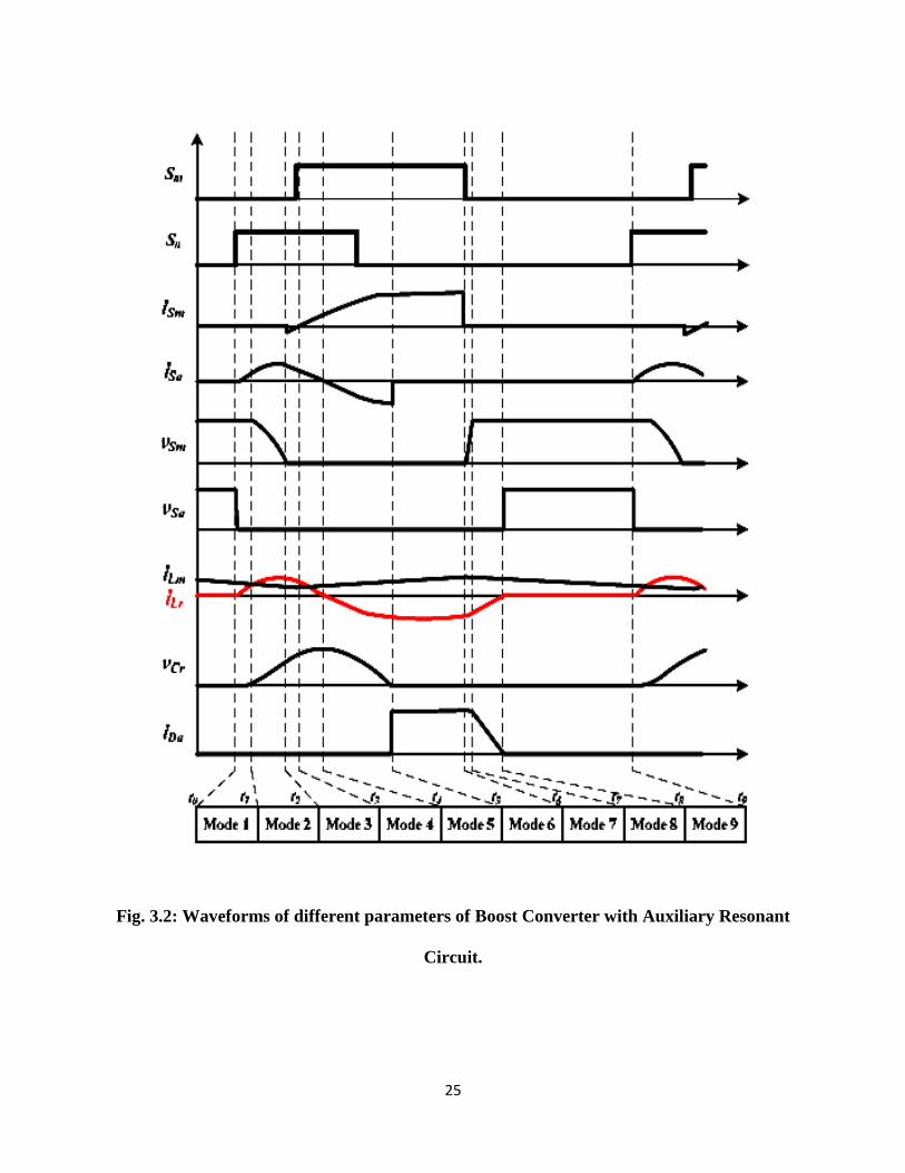
25
Fig. 3.2: Waveforms of different parameters of Boost Converter with Auxiliary Resonant
Circuit.
26
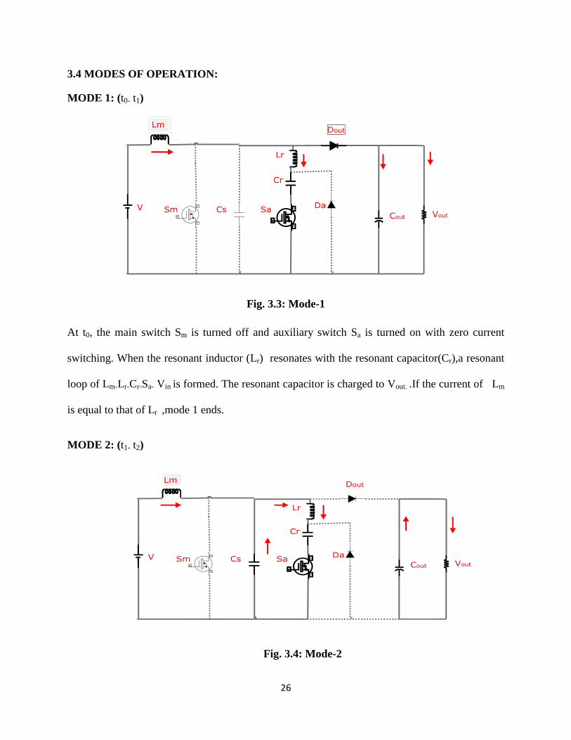
3.4 MODES OF OPERATION:
MODE 1: (t0- t1)
Fig. 3.3: Mode-1
At t0, the main switch Sm is turned off and auxiliary switch Sa is turned on with zero current
switching. When the resonant inductor (Lr) resonates with the resonant capacitor(Cr),a resonant
loop of Lm-Lr-Cr-Sa- Vin is formed. The resonant capacitor is charged to Vout. .If the current of Lm
is equal to that of Lr ,mode 1 ends.
MODE 2: (t1- t2)
Fig. 3.4: Mode-2
27
The current through Lr continues to increase due to resonance between Lr and Cr . The charged in
the snubber capacitor (Cs) starts to discharge and mode 2 ends when the voltage of Cr is to zero.
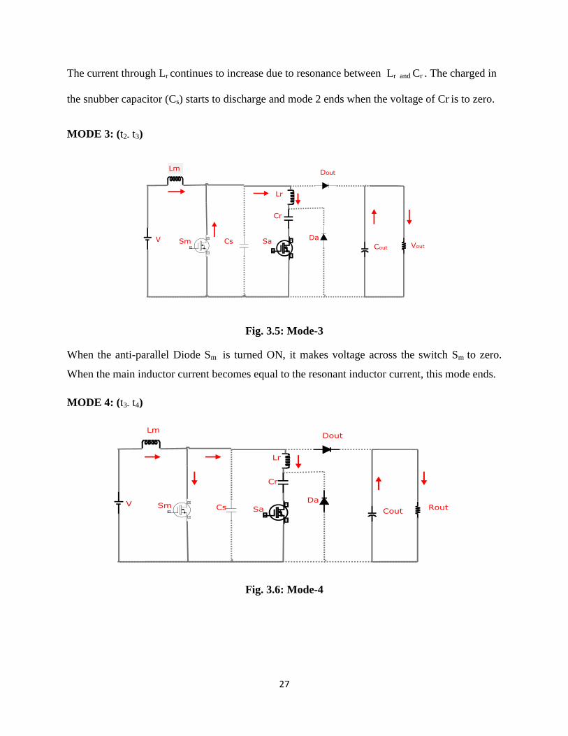
MODE 3: (t2- t3)
Fig. 3.5: Mode-3
When the anti-parallel Diode Sm is turned ON, it makes voltage across the switch Sm to zero.
When the main inductor current becomes equal to the resonant inductor current, this mode ends.
MODE 4: (t3- t4)
Fig. 3.6: Mode-4
28
The main switch Sm is turned ON, when the voltage is zero. The resonant circuit is charged
continuously through the capacitor.
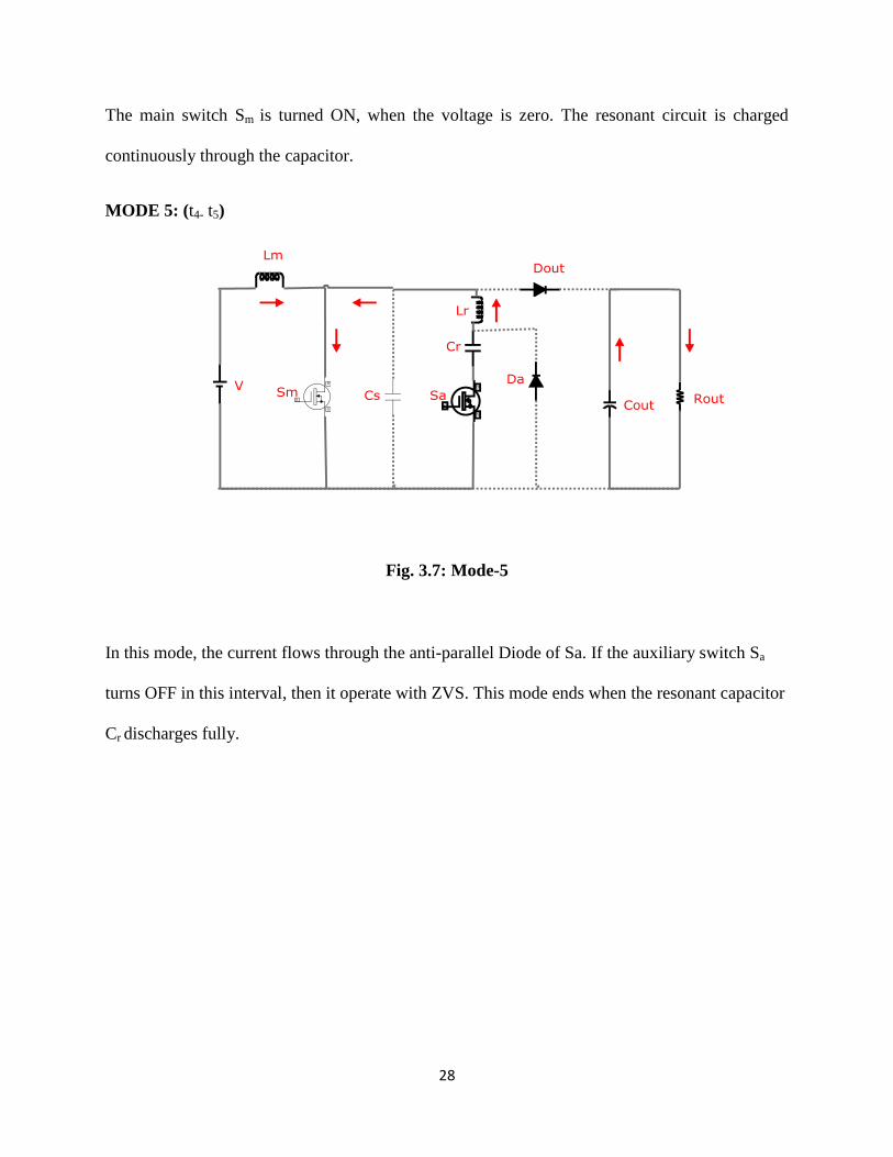
MODE 5: (t4- t5)
Fig. 3.7: Mode-5
In this mode, the current flows through the anti-parallel Diode of Sa. If the auxiliary switch Sa
turns OFF in this interval, then it operate with ZVS. This mode ends when the resonant capacitor
Cr discharges fully.
29
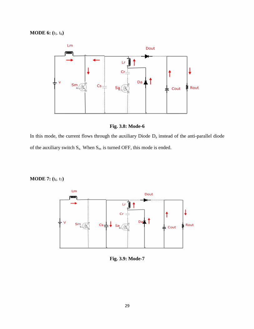
MODE 6: (t5- t6)
Fig. 3.8: Mode-6
In this mode, the current flows through the auxiliary Diode Da instead of the anti-parallel diode
of the auxiliary switch Sa. When Sm is turned OFF, this mode is ended.
MODE 7: (t6- t7)
Fig. 3.9: Mode-7
30
The main switch is turned ON with ZVS by the snubber capacitor. Energy is stored in the
snubber capacitor Cs . When the Cs is fully charged, this mode ends.
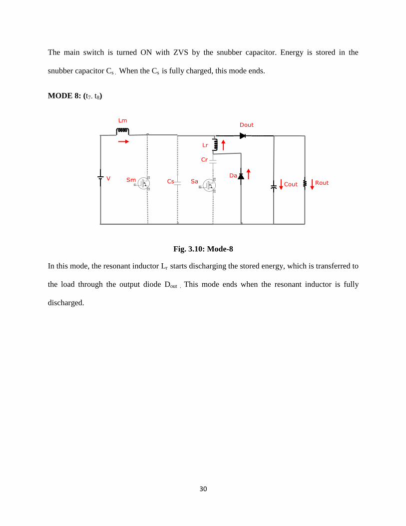
MODE 8: (t7- t8)
Fig. 3.10: Mode-8
In this mode, the resonant inductor Lr starts discharging the stored energy, which is transferred to
the load through the output diode Dout . This mode ends when the resonant inductor is fully
discharged.
31
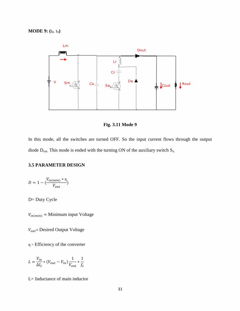
MODE 9: (t8- t9)
Fig. 3.11 Mode 9
In this mode, all the switches are turned OFF. So the input current flows through the output
diode Dout. This mode is ended with the turning ON of the auxiliary switch Sa.
3.5 PARAMETER DESIGN
D= Duty Cycle
Minimum input Voltage
= Desired Output Voltage
= Efficiency of the converter
L= Inductance of main inductor
32
= Switching Frequency
= estimated inductor ripple current
= Maximum output current
= Minimum Output Capacitance
= Additional output voltage ripple due to capacitors ESR
ESR= Equivalent series resistance of the output capacitor
The values of parameters calculated using these equations are as follows:
Main Inductor (L) = 160 µH
Snubber Capacitor (C) = 1200 nF
3.5 CONCLUSION
In this chapter Boost Converter with auxiliary resonant circuit is presented. Different modes of
operation of the converter are studied. The different parameters of the proposed converter are
designed using the given mathematical equations.
33
CHAPTER 4
SIMULATION RESULTS
AND DISCUSSION
34
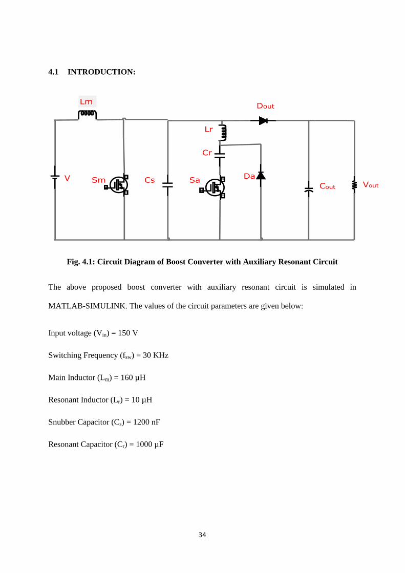
4.1 INTRODUCTION:
Fig. 4.1: Circuit Diagram of Boost Converter with Auxiliary Resonant Circuit
The above proposed boost converter with auxiliary resonant circuit is simulated in
MATLAB-SIMULINK. The values of the circuit parameters are given below:
Input voltage (Vin) = 150 V
Switching Frequency (fsw) = 30 KHz
Main Inductor (Lm) = 160 µH
Resonant Inductor (Lr) = 10 µH
Snubber Capacitor (Cs) = 1200 nF
Resonant Capacitor (Cr) = 1000 µF
35
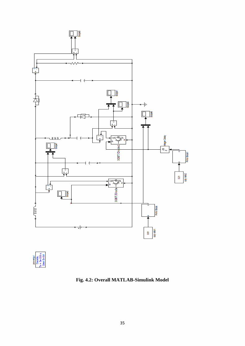
Fig. 4.2: Overall MATLAB-Simulink Model
36
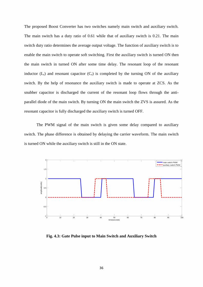
The proposed Boost Converter has two switches namely main switch and auxiliary switch.
The main switch has a duty ratio of 0.61 while that of auxiliary switch is 0.21. The main
switch duty ratio determines the average output voltage. The function of auxiliary switch is to
enable the main switch to operate soft switching. First the auxiliary switch is turned ON then
the main switch in turned ON after some time delay. The resonant loop of the resonant
inductor (Lr) and resonant capacitor (Cr) is completed by the turning ON of the auxiliary
switch. By the help of resonance the auxiliary switch is made to operate at ZCS. As the
snubber capacitor is discharged the current of the resonant loop flows through the anti-
parallel diode of the main switch. By turning ON the main switch the ZVS is assured. As the
resonant capacitor is fully discharged the auxiliary switch is turned OFF.
The PWM signal of the main switch is given some delay compared to auxiliary
switch. The phase difference is obtained by delaying the carrier waveform. The main switch
is turned ON while the auxiliary switch is still in the ON state.
Fig. 4.3: Gate Pulse input to Main Switch and Auxiliary Switch
0 10 20 30 40 50 60 70 80 90 100-1
-0.5
0
0.5
1
1.5
2
time(seconds)
am
plit
ude(v
olts)
main switch PWM
auxiliary switch PWM
37
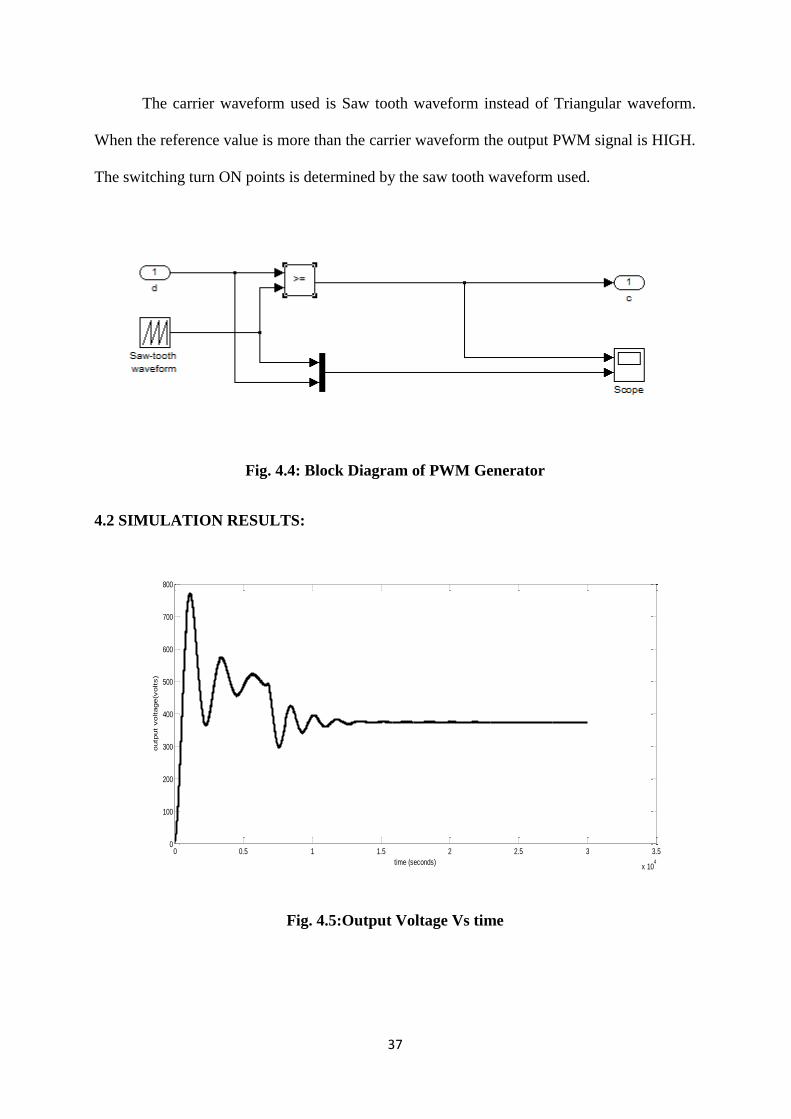
The carrier waveform used is Saw tooth waveform instead of Triangular waveform.
When the reference value is more than the carrier waveform the output PWM signal is HIGH.
The switching turn ON points is determined by the saw tooth waveform used.
Fig. 4.4: Block Diagram of PWM Generator
4.2 SIMULATION RESULTS:
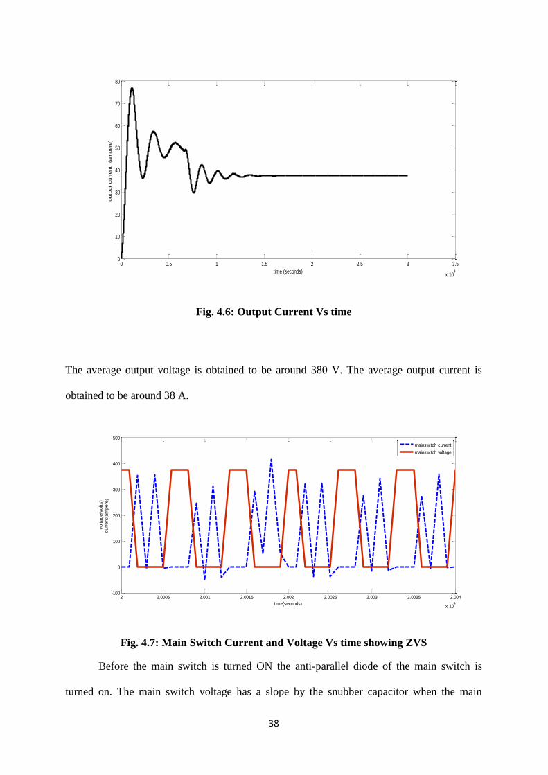
Fig. 4.5:Output Voltage Vs time
0 0.5 1 1.5 2 2.5 3 3.5
x 104
0
100
200
300
400
500
600
700
800
time (seconds)
outp
ut
voltage(v
olts)
38
Fig. 4.6: Output Current Vs time
The average output voltage is obtained to be around 380 V. The average output current is
obtained to be around 38 A.
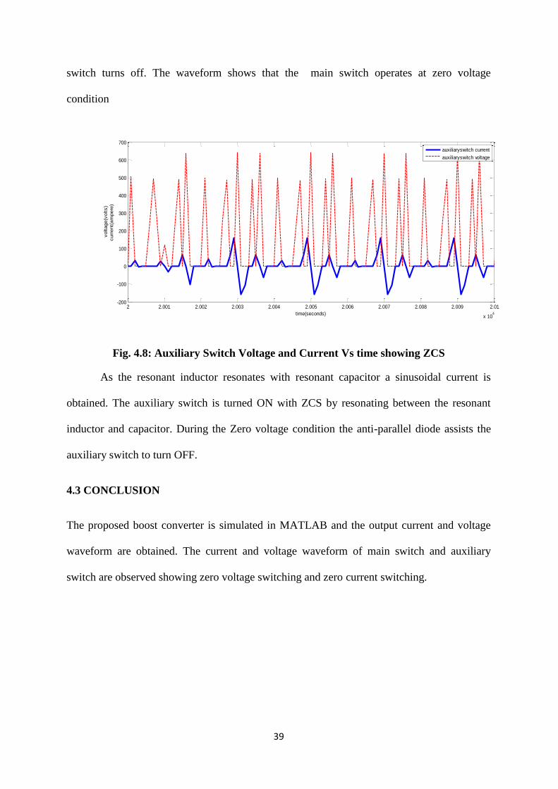
Fig. 4.7: Main Switch Current and Voltage Vs time showing ZVS
Before the main switch is turned ON the anti-parallel diode of the main switch is
turned on. The main switch voltage has a slope by the snubber capacitor when the main
0 0.5 1 1.5 2 2.5 3 3.5
x 104
0
10
20
30
40
50
60
70
80
time (seconds)
outp
ut
curr
ent
(am
pere
)
2 2.0005 2.001 2.0015 2.002 2.0025 2.003 2.0035 2.004
x 104
-100
0
100
200
300
400
500
time(seconds)
voltage(v
olts)
curr
ent(
am
pere
)
mainswitch current
mainswitch voltage
39
switch turns off. The waveform shows that the main switch operates at zero voltage
condition
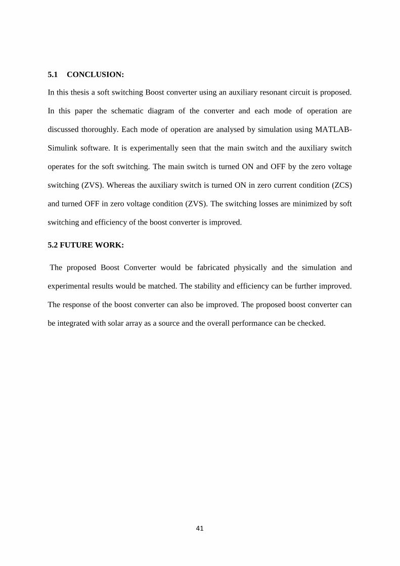
Fig. 4.8: Auxiliary Switch Voltage and Current Vs time showing ZCS
As the resonant inductor resonates with resonant capacitor a sinusoidal current is
obtained. The auxiliary switch is turned ON with ZCS by resonating between the resonant
inductor and capacitor. During the Zero voltage condition the anti-parallel diode assists the
auxiliary switch to turn OFF.
4.3 CONCLUSION
The proposed boost converter is simulated in MATLAB and the output current and voltage
waveform are obtained. The current and voltage waveform of main switch and auxiliary
switch are observed showing zero voltage switching and zero current switching.
2 2.001 2.002 2.003 2.004 2.005 2.006 2.007 2.008 2.009 2.01
x 104
-200
-100
0
100
200
300
400
500
600
700
time(seconds)
voltage(v
olts)
curr
ent(
am
pere
)
auxiliaryswitch current
auxiliaryswitch voltage

40
CHAPTER 5
CONCLUSION AND
FUTURE WORK
41
5.1 CONCLUSION:
In this thesis a soft switching Boost converter using an auxiliary resonant circuit is proposed.
In this paper the schematic diagram of the converter and each mode of operation are
discussed thoroughly. Each mode of operation are analysed by simulation using MATLAB-
Simulink software. It is experimentally seen that the main switch and the auxiliary switch
operates for the soft switching. The main switch is turned ON and OFF by the zero voltage
switching (ZVS). Whereas the auxiliary switch is turned ON in zero current condition (ZCS)
and turned OFF in zero voltage condition (ZVS). The switching losses are minimized by soft
switching and efficiency of the boost converter is improved.
5.2 FUTURE WORK:
The proposed Boost Converter would be fabricated physically and the simulation and
experimental results would be matched. The stability and efficiency can be further improved.
The response of the boost converter can also be improved. The proposed boost converter can
be integrated with solar array as a source and the overall performance can be checked.
42
REFERENCES
[1] S.H. Park,G.R. Cha, Y.C. Jung and C.Y. Won, “Design and application for PV generation
system using a soft switching boost converter with SARC,” IEEE Trans. On Industrial
Electronics, vol. 57, no. 2, pp515-522, February 2010.
[2] S.H. Park, S.R. Park, J.S. Yu, Y.C. Jung and C.Y. Won, “Analysis and design of a soft
switching boost converter with an HI-bridge auxiliary resonant circuit,” IEEE Trans. on
Power Electronics, vol. 25, no. 8, pp. 2142-2149, August 2010.
[3] E.H. Kim and B.H. Kwon, “Zero-voltage- and zero current- switching full-bridge
converter with secondary resonance,” IEEE Trans. on Industrial Electronics, vol. 57,
no. 3, pp. 1017-1025, March 2010.
[4] Charles J. McAtee, Jai P. Agrawal and Hassan Moghbelli, “A 100 watt power supply
using ZVS boost converter,” Applied Power Electronics Conference and Exposition
1995(APEC 1995), Dallas(USA), March 1995.
[5] Miroslaw Luft, Elzbieta Szychta and Leszek Szychta, “Method of designing ZVS boost
converter,” Power Electronics and Motion Control Conference 2008(EPEPEMC
2008), Poznan(Poland), September 2008.
[6] Hacy Bodur and A. Faruk Bakan, “A new ZVT-PWM DCDC converter,” IEEE Trans. on
Power Electronics, vol. 17, no. 1, pp. 40-47, January 2002.
[7] R. Gurunathan and A. K. S. Bhat, “A zero-voltage transition boost converter using a zero-
voltage switching auxiliary circuit,” IEEE Trans. on Power Electronics, vol. 17, no. 5, pp.
658-668, September 2002.
[8] Chien-Ming Wang, “Novel zero-voltage-transition PWM DC-DC converters,” IEEE
Trans. on Industrial Electronics, vol. 53, no. 1, pp. 254-262, February 2006.
[9] R. Gurunathan and A. K. S. Bhat, “ZVT boost converter using a ZCS auxiliary circuit,”
IEEE Trans. on Aerospace and Electronic System, vol. 37, no. 3, pp. 889-897

43
APPENDIX
44
250mV input boost converter for low power application
This project concerns about low power boost converter designed to operate at very low input
voltage of 250mV. It’s the voltage range of micro energy sources such as photo voltaic cells.
The PCB prototype will provide a regulated maximum output voltage of 3.3V with 70% of
maximum efficiency. The low power range of micro energy sources requires highly efficient
circuit adaptation. The proposed converter design is very attractive for low power application
power supply. The converter works without any external power supply for the control logic.
New energy sources like single solar cell modules, thin-film batteries or micro fuel cells have
been innovated in the last years. These sources have higher energy density than the traditional
power supply sources. The traditional power supply sources such as Li-Ion or Ni-MH
batteries have some significant limitations in terms of supply current and voltage. Hence we
are trying to design a circuit highly efficient to work with input power of very few hundreds
of Ws with maximum life time.
Fig. 1: Circuit Architecture of DC-DC Boost Converter
45
The proposed circuit consists of 4 main buildings. They are
i. Cross coupled differential oscillator
ii. Intermediate Boost Stage
iii. Final Boost Stage
iv. Feedback Control Stage
1.1 Cross coupled Differential oscillator
The circuit consists of a cross-coupled pair of zero threshold voltage mosfets to implement
the negative resistance required for circuit oscillation. The oscillator generates a sinusoidal
waveform with ∼0.5V peak-to-peak amplitude and 0.25V DC offset. The oscillation
frequency of DC-DC boost converters, is fixed at ∼170 kHz. Increasing frequency leads to
higher efficiency in boost DC-DC converters, since this allows using smaller inductors with
lower parasitic resistances, thus decreasing related power losses. At the same time, higher
frequencies lead to a higher power consumption of comparators required to control MOSFET
switches. The use of cross coupled differential scheme is adopted because
- Noise and disturbances are reduced.
- MOSFET switches can be biased directly through the inductors.
- Guarantees the correct turn on and turn off of the MOSFET switches.
The MOSFET used in the circuit is ALD110800 having zero threshold voltage. It allows
taking an input of very low voltage of 250mV. Diodes at the oscillator outputs are inserted to
limit maximum oscillation amplitudes.
46
1.2 Intermediate DC-DC boost stage
This stage comprised of three blocks. i.e
1. Voltage clamp
2. First boost stage
3. Second boost stage
The voltage clamp stage is used to add to the control signal and generated by the
differential oscillator a DC-offset voltage equal to the threshold voltage of the MOSFET
switches of the two boost converters M3 and M4, which is ∼0.6 V.It allows the MOSFET
switch of both first and second boosts stage to operate with 50% duty cycle. Thus each boost
converter doubles its input voltage and the final 4x needed for the FBS comparator
supply is generated. Either increase or decrease in the duty cycle of the MOSFET increases
the power loss in it.
1.3 Final boost stage
It is a conventional DC to D boost stage which converts voltage from 250mV to 3.3V.PWM
control signal is generated by comparing the sinusoidal voltage provided by the differential
oscillator to the constant control voltage generated by the feedback control stage, . The
comparator performing this operation is the most critical component for the efficiency of the
whole circuit To achieve a high efficiency, we used the low-voltage and low-power rail-to-
rail comparator ON Semiconductors NCS2200.Despite the low power consumption
(minimum supply voltage ∼0.85V and 15μA bias current), this comparator features very low
output voltage rise and fall times (20ns with a load capacitor of 50pF, corresponding to the
M6 input capacitance, thus allowing strongly reducing power losses at MOSFET switch turn-
on and turn-off and significantly improving the efficiency of the whole DC-DC boost
47
converter. FBS is the real DC-DC boost stage converting the power provided from the micro
energy source, hence maximizing its efficiency is crucial to improve the efficiency of the
whole converter.The inefficiencies of other building blocks lead to much smaller energy
dissipation, thus penalizing less the whole circuit efficiency, as the power they handle is only
a relatively small fraction of the total power available from the micro energy source.
1.4Feedback Control Stage
The circuit is consists of an error amplifier and a compensation network required to assure
circuit stability. The error amplifier is used to amplify the voltage difference –
is the reference voltage of the feedback control network. Here resistors are used to
limit the maximum current through the diodes. So Thus, is approximately given by the
knee voltage of the diode. Of course, this solution suffers from the poor precision due to
unpredictable variations of the electrical characteristics of the diodes with process and
temperature, but has also the great advantage of strongly reducing the power consumption
compared to more precise band gap voltage reference solutions. is the output voltage,
scaled down by the variable resistance divider, which is comprises of R1 andR2. Changing
the resistance R1 allows setting the output voltage Vout.
48
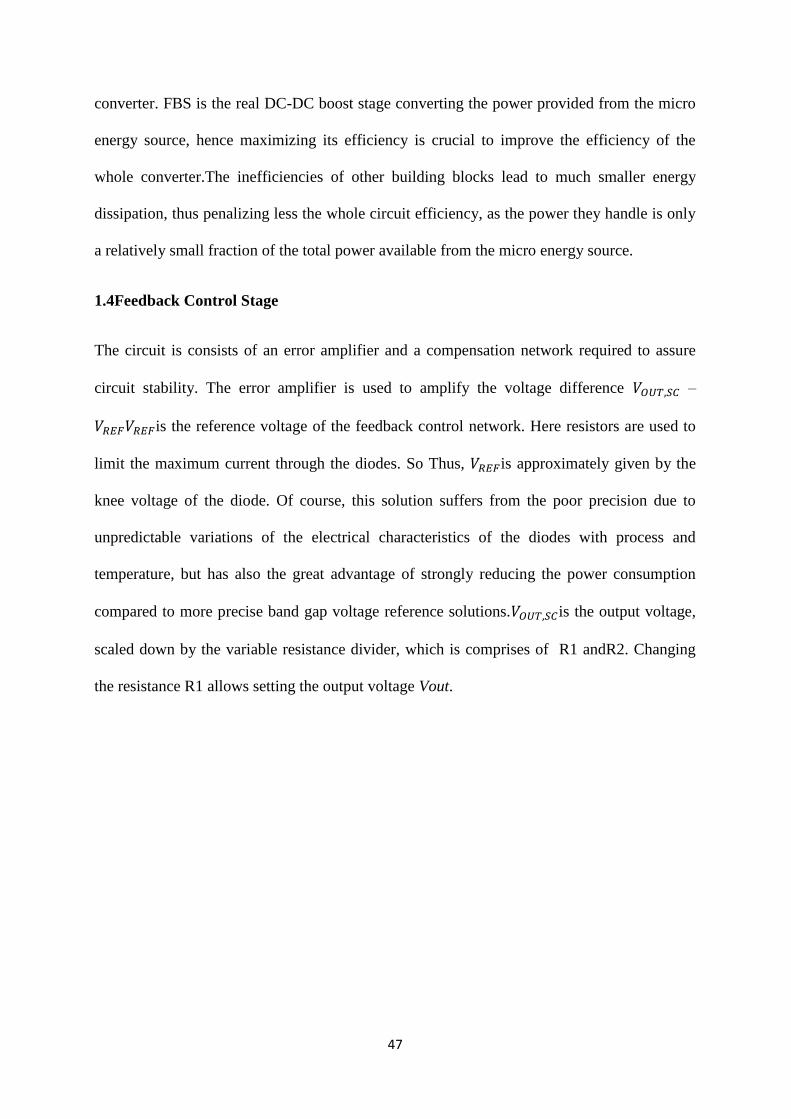
Fig. 2. Differential Oscillator Voltage Vs Time
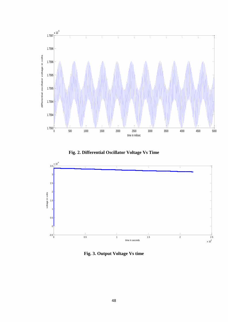
Fig. 3. Output Voltage Vs time
0 500 1000 1500 2000 2500 3000 3500 4000 4500 50001.7593
1.7594
1.7594
1.7595
1.7595
1.7596
1.7596
1.7597x 10
-6
time in milisec
differentia
l oscilla
tor voltage in
volts
0 0.5 1 1.5 2 2.5
x 106
-0.5
0
0.5
1
1.5
2
2.5
3
3.5x 10
-6
time in seconds
voltage in v
olts
49
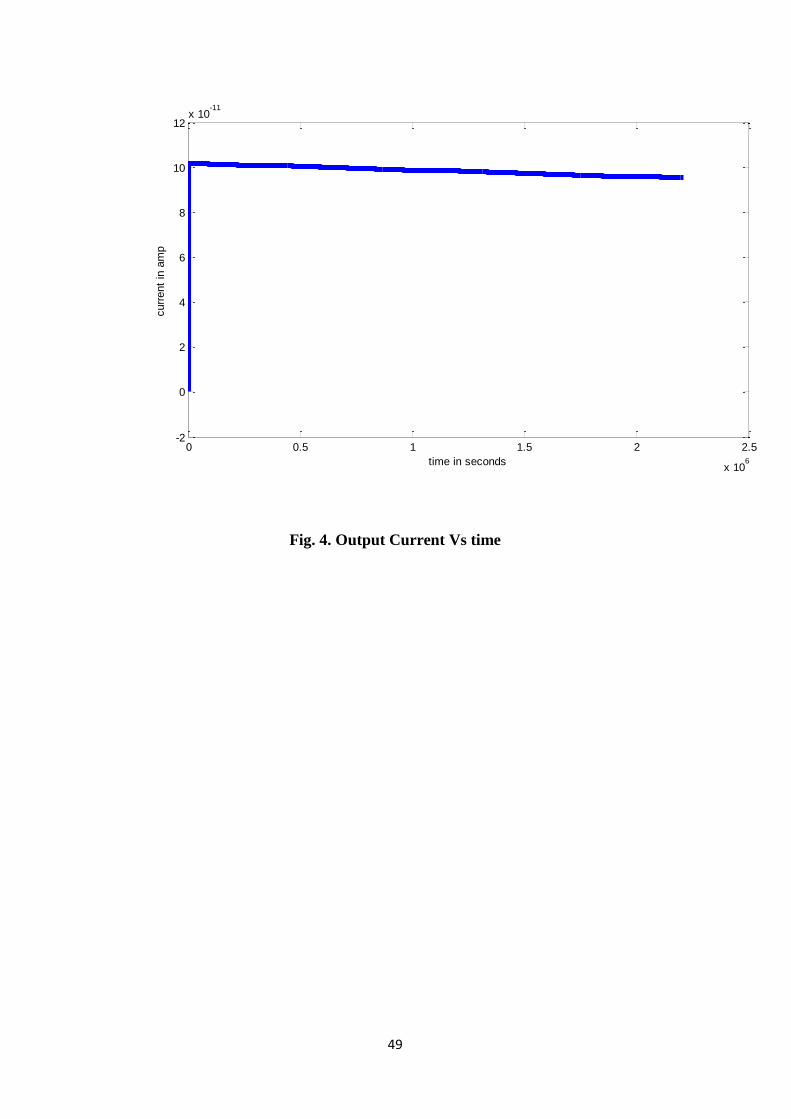
Fig. 4. Output Current Vs time
0 0.5 1 1.5 2 2.5
x 106
-2
0
2
4
6
8
10
12x 10
-11
time in seconds
curr
ent
in a
mp
![Crow Search Optimized Control of Photovoltaic …A DC -DC converter [6], buck boost converter [7], Luo converter [8], canonical switching cell (CSC) converter [9], zeta converter [10]](https://img.pdfslide.net/doc/110x75/5fcf5114fee703425c72d389/crow-search-optimized-control-of-photovoltaic-a-dc-dc-converter-6-buck-boost.jpg)


![Bridgeless Buck-Boost PFC Converter for Multistring LED Driver€¦ · boost converter as a universal PFC converter [6]. In order to address these issues, a buck-boost converter is](https://img.pdfslide.net/doc/110x75/5eaabf2a4ab79d1e774f9005/bridgeless-buck-boost-pfc-converter-for-multistring-led-driver-boost-converter-as.jpg)