Embed Size (px)
Citation preview
Sub-diffraction Laser Synthesis of SiliconNanowiresJames I. Mitchell, Nan Zhou, Woongsik Nam, Luis M. Traverso & Xianfan Xu
School of Mechanical Engineering, Birck Nanotechnology Center Purdue University, West Lafayette, Indiana 47907.
We demonstrate synthesis of silicon nanowires of tens of nanometers via laser induced chemical vapordeposition. These nanowires with diameters as small as 60 nm are produced by the interference betweenincident laser radiation and surface scattered radiation within a diffraction limited spot, which causesspatially confined, periodic heating needed for high resolution chemical vapor deposition. By controllingthe intensity and polarization direction of the incident radiation, multiple parallel nanowires can besimultaneously synthesized. The nanowires are produced on a dielectric substrate with controlled diameter,length, orientation, and the possibility of in-situ doping, and therefore are ready for device fabrication. Ourmethod offers rapid one-step fabrication of nano-materials and devices unobtainable with previous CVDmethods.
Since the initial description of nanowire synthesis via the vapor-liquid-solid (VLS) mechanism1,2, nanowireshave garnered significant attention as a means of constructing nano-devices with a wide breadth ofapplications3–5 due to their fine dimensions6 and variety of materials and structures7. Despite this potential,
the lack of control in growth, placement and orientation compounded by potential contamination from metalcatalysts still hinders more widespread implementation. Guiding nanowire formation8–10 and eliminating metalprecursors11 have been attempted, but have not entirely overcome these obstacles. Here, we demonstrate synthesisof silicon nanowires with diameters of 60 nm via laser induced chemical vapor deposition (CVD). We producenanowires by utilizing interference between incident laser radiation and surface scattered radiation that generatesspatially confined, periodic heating needed for obtaining nanowires with diameters far below the diffraction limit.By controlling the intensity and polarization direction of the incident laser radiation, single or multiple parallelnanowires are synthesized on a dielectric substrate with controlled diameter, length, orientation, and the pos-sibility of in-situ doping, making them ready for device fabrication.
Direct chemical synthesis of materials by laser illumination has been used to fabricate valuable electrical andphotonic components12–14, but the feature sizes were limited to hundreds of nanometers due to the diffractionlimit of light. On the other hand, laser based methods including multiphoton polymerization15, stimulatedemission depletion of polymers16,17, and near field plasmonic processing18–20 have achieved features with criticaldimensions of tens of nanometers, but these methods generally cannot be directly implemented for nano-materials growth. It is therefore useful to develop a method capable of combining the fine features of subdiffraction limit laser growth with direct material synthesis. Here we describe a laser-based method to producesilicon nanowires with widths of about 60 nm, directly on a dielectric substrate, with controlled length, orienta-tion, and in-situ doping.
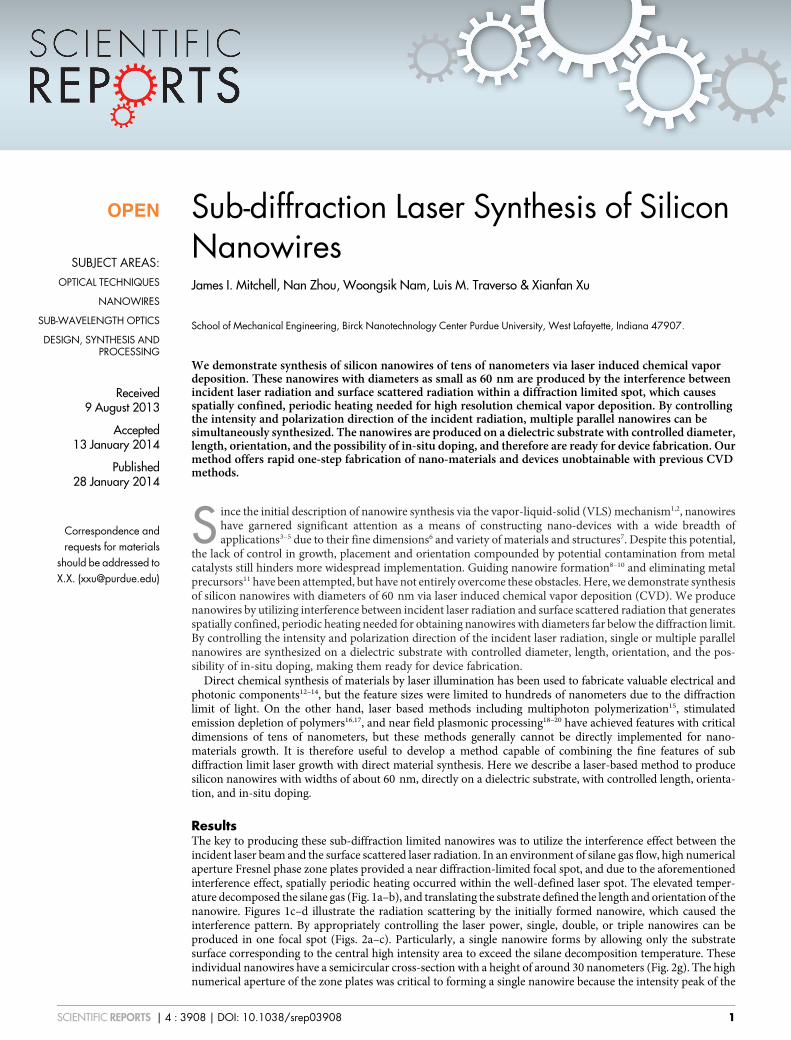
ResultsThe key to producing these sub-diffraction limited nanowires was to utilize the interference effect between theincident laser beam and the surface scattered laser radiation. In an environment of silane gas flow, high numericalaperture Fresnel phase zone plates provided a near diffraction-limited focal spot, and due to the aforementionedinterference effect, spatially periodic heating occurred within the well-defined laser spot. The elevated temper-ature decomposed the silane gas (Fig. 1a–b), and translating the substrate defined the length and orientation of thenanowire. Figures 1c–d illustrate the radiation scattering by the initially formed nanowire, which caused theinterference pattern. By appropriately controlling the laser power, single, double, or triple nanowires can beproduced in one focal spot (Figs. 2a–c). Particularly, a single nanowire forms by allowing only the substratesurface corresponding to the central high intensity area to exceed the silane decomposition temperature. Theseindividual nanowires have a semicircular cross-section with a height of around 30 nanometers (Fig. 2g). The highnumerical aperture of the zone plates was critical to forming a single nanowire because the intensity peak of the
OPEN
SUBJECT AREAS:OPTICAL TECHNIQUES
NANOWIRES
SUB-WAVELENGTH OPTICS
DESIGN, SYNTHESIS ANDPROCESSING
Received9 August 2013
Accepted13 January 2014
Published28 January 2014
Correspondence andrequests for materials
should be addressed toX.X. ([email protected])
SCIENTIFIC REPORTS | 4 : 3908 | DOI: 10.1038/srep03908 1
focal spot must be narrow enough so that only the central peak of theinterference fringes has sufficient intensity for heating the substratein excess of the silane deposition temperature.
To further illustrate the forming of the nanowire patterns,Figs. 2d–f show the nanowire shape and orientation dependenceon the polarization of the incident radiation. Fig. 2d and Fig. 2edemonstrate nanowire patterns 45 degrees from the vertical directionand in the vertical direction, respectively, which match the laserpolarization direction. We also tested the effect of using circularlypolarized light, resulting in nanowires hundreds of nanometers indiameter. With in situ doping of boron using diborane together withsilane, these thick wires which were essentially agglomerations ofthinner nanowires, yielded rough surfaces (Fig. 2f) which gaveimproved sensitivity for chemical detection21.
The laser induced nano-structures used here for nanowire forma-tion, have been observed elsewhere for high power situations whereintense laser pulses ablate material to form nanoscale ripples orgrooves on the substrate. In these other cases, the substrate materiallargely determines both the periodicity (L) of the ripples as well asthe direction they form relative to the polarization direction of theincident laser radiation22. The periodicity is often divided into tworegimes depending on the wavelength (l): low spatial frequency forl . L . 0.4 l and high spatial frequency for 0.4 l . L23. Lowspatial frequency ripples are often described as forming when theincoming laser radiation interferes with radiation scattered from thesubstrate to create high radiation intensity distributions that removethe material24. It has been shown that this restructuring can act as afeedback mechanism which decreases the ripple spacing as the num-ber of laser pulses increases22,23,25. On some dielectric surfaces, and inparticular silicon dioxide, low spatial frequency ripples form parallelto the laser’s electric field polarization direction22. Interferencebetween incident radiation and surface or volume plasmons causedby the incident radiation has been suggested as part of the mech-anism for producing ripples on metal surfaces26, on semiconductorsurfaces23,25, or for dielectric materials where the laser power is highenough to generate sufficient free electrons to cause the material toact metallically23,27. In these cases, the ripples are perpendicular to thepolarization direction of the incident laser beam since interferenceoccurs when the component of the electrical field of the surfaceplasmon, along its propagation direction and perpendicular to theripples, is in the same direction as the electrical field of the incominglaser.
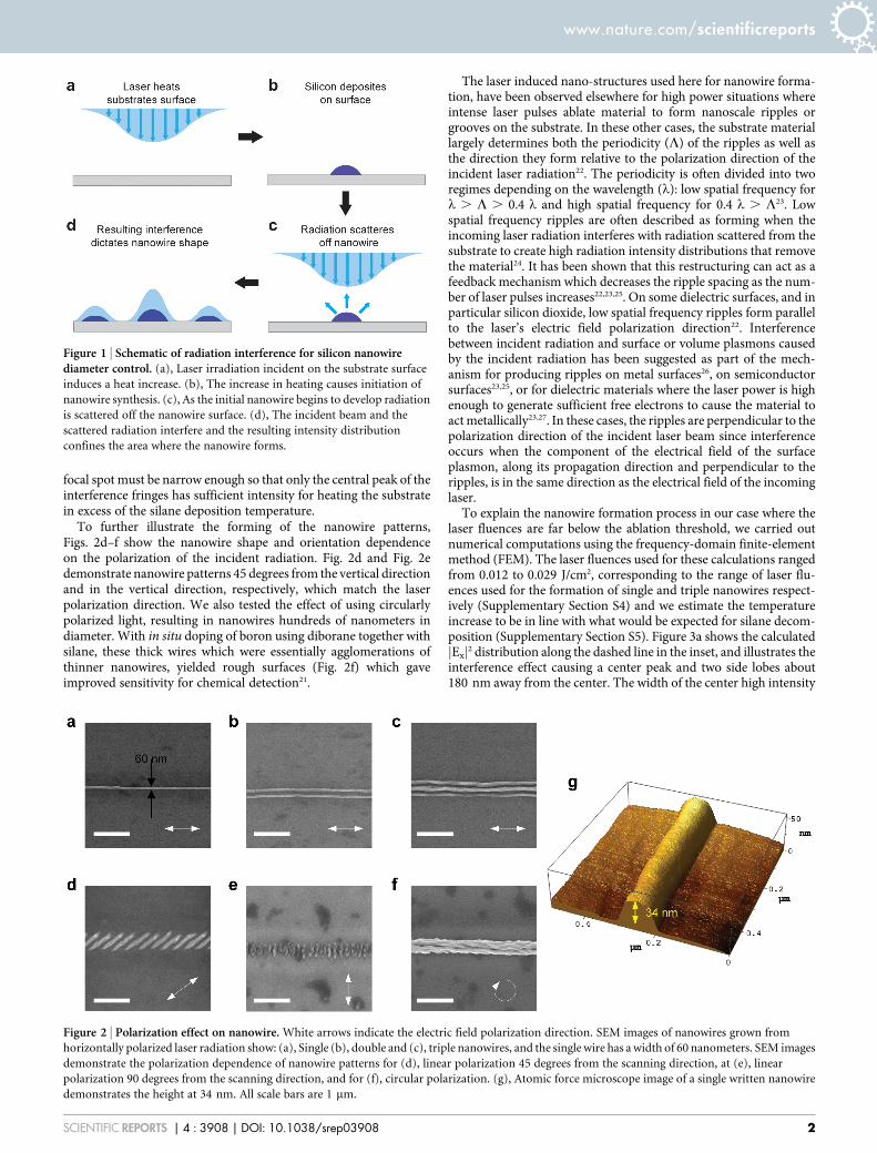
To explain the nanowire formation process in our case where thelaser fluences are far below the ablation threshold, we carried outnumerical computations using the frequency-domain finite-elementmethod (FEM). The laser fluences used for these calculations rangedfrom 0.012 to 0.029 J/cm2, corresponding to the range of laser flu-ences used for the formation of single and triple nanowires respect-ively (Supplementary Section S4) and we estimate the temperatureincrease to be in line with what would be expected for silane decom-position (Supplementary Section S5). Figure 3a shows the calculatedjExj2 distribution along the dashed line in the inset, and illustrates theinterference effect causing a center peak and two side lobes about180 nm away from the center. The width of the center high intensity
Figure 1 | Schematic of radiation interference for silicon nanowirediameter control. (a), Laser irradiation incident on the substrate surface
induces a heat increase. (b), The increase in heating causes initiation of
nanowire synthesis. (c), As the initial nanowire begins to develop radiation
is scattered off the nanowire surface. (d), The incident beam and the
scattered radiation interfere and the resulting intensity distribution
confines the area where the nanowire forms.
Figure 2 | Polarization effect on nanowire. White arrows indicate the electric field polarization direction. SEM images of nanowires grown from
horizontally polarized laser radiation show: (a), Single (b), double and (c), triple nanowires, and the single wire has a width of 60 nanometers. SEM images
demonstrate the polarization dependence of nanowire patterns for (d), linear polarization 45 degrees from the scanning direction, at (e), linear
polarization 90 degrees from the scanning direction, and for (f), circular polarization. (g), Atomic force microscope image of a single written nanowire
demonstrates the height at 34 nm. All scale bars are 1 mm.
www.nature.com/scientificreports
SCIENTIFIC REPORTS | 4 : 3908 | DOI: 10.1038/srep03908 2
region is restricted by the interference effect to about 59 nm fullwidth half maximum. If the laser fluence increases, the intensity atthe two side lobes will exceed the threshold to form triple lines. The 2-D jExj2 distribution on the silicon dioxide surface (inset of Fig. 3a)shows high intensities at the wire tip and the two side lobe-like areas.The field at the tip of the wire has higher intensity, shown in the jExj2distribution along the dashed line in the inset of Fig. 3b, and this highintensity at the tip leads the nanowire formation. Similarly, for theformation of three wires, the electrical field distribution in Fig. 3c
shows the high intensity areas at the tips of the three wires causing thenanowire growth.
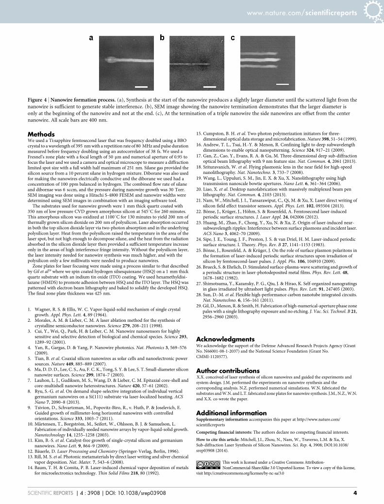
The explanation given above is further supported by noting that atthe beginning of nanowire growth, there is no scattering and nointerference, therefore creating a large initial wire diameter(Fig. 4a). Although the initial diameter is large, it is quickly reducedas the interference begins to affect formation. Correspondingly, thewire termination should demonstrate no enlargement of the dia-meter as verified in Fig. 4b. Simulations also show that for triple wireformations the center wire is longer than the two side wires (Fig. 3ainset). The highest intensities of the two side lobes are at the samelengthwise locations as the center of the laser spot, whereas the high-est intensity along the center nanowire is in front of the laser spot,and this effect is seen at the end of the triple nanowires when the laserradiation is terminated (Fig. 4c). If the polarization direction of theincident laser beam is not completely parallel to the substrate scan-ning direction, the number of nanowires can fluctuate as the front ofthe nanowire moves off the center of the laser irradiation, and can beresponsible for the formation of two nanowires where each nanowireprovides the scattered radiation for the other (Fig. S1).
We emphasize that for our nanowire synthesis the interferencebetween the incident and scattered laser radiation forms interferencefringes for nanowire synthesis, and the plasmonic effect does not playa role. We carried out non-linear ultrafast pulse propagation calcula-tions in silicon dioxide (Supplementary Section S2) considering themulti-photon absorption effect, the resulting free electron density,and the modifications to the dielectric constant. At the laser fluencesfor nanowire synthesis, the free electron density is less than 6 3
1019 cm23, which is more than two orders of magnitude lowerthan the critical free electron density for the material to behavemetallically. Therefore, surface plasmons do not contribute to theinterference effect we demonstrate here, in contrast to the case offemtosecond laser ablation of most dielectric materials23,27. Further-more, the fringes formed by the interference between the incidentradiation and the induced surface plasmons are perpendicular to thelaser polarization direction, whereas the nanowires we grew formparallel to the polarization direction. We verify using numericalsimulation that if the laser power is high enough, interference fringescan form perpendicular to the polarization direction (Fig. S2).
DiscussionWhile other processes for synthesizing nanowires are limited inplacement precision, resolution, or flexibility due to the stringentrequirements to create features with critical dimensions of tens ofnanometers, our laser synthesis method for producing nanowiresprovides a means for creating nanowires laying horizontally on adielectric substrate which electrically insulates the nanowires, withprecise location, length, orientation, and in-situ doping allowing foreasy integration of these nanowires into devices. With typical laserpowers on the order of watts, an array of Fresnel’s zone plates cangenerate hundreds of light spots for parallel writing to scale up thenanowire synthesis process. This could be of particular use in pro-ducing devices on transparent insulating materials or for thin filmtransistors where precisely placed nanowires could simplify man-ufacturing and increase device performance28.
In this work we demonstrated a laser induced CVD method cap-able of fabricating nanowires far below the diffraction limit withwidths of only 60 nm using far-field optics. We utilized the interfer-ence between scattered laser radiation and radiation incident on thesubstrate surface to obtain these narrow widths. We confirmed thenanowire formation mechanism by performing electromagnetic fieldsimulations which agreed with the phenomena observed in theexperiments. This nanowire fabrication method provides a meansto precisely place nanowires for a device and can serve as a usefulplatform for nanofabrication of a variety of materials and devices.
Figure 3 | Computational results of electrical field ( | Ex | 2) distributionsduring nanowire synthesis. The distribution for a single nanowire at two
laser fluences is displayed along two scan lines in (a) and (b). The left inset
in (b) shows the highest intensity is located at the wire tip. (c), Intensity
distribution for triple nanowires. In (c) the spacing between wires is
180 nm and the central wire is 125 nm longer than those wires to the side.
The simulated wires are 60 nm wide, 30 nm high with a semi-circular cross
section. The intensity was normalized to the maximum value at the fluence
of 0.029 J/cm2. For all simulations, the electric field polarization of the
incoming laser was parallel to the wires.
www.nature.com/scientificreports
SCIENTIFIC REPORTS | 4 : 3908 | DOI: 10.1038/srep03908 3
MethodsWe used a Ti:sapphire femtosecond laser that was frequency doubled using a BBOcrystal to a wavelength of 395 nm with a repetition rate of 80 MHz and pulse durationmeasured before frequency doubling using an autocorrelator of 38 fs. We used aFresnel’s zone plate with a focal length of 50 mm and numerical aperture of 0.95 tofocus the laser and we used a camera and optical microscope to measure a diffractionlimited spot size with a full width half maximum of 251 nm. Silane gas provided thesilicon source from a 10 percent silane in hydrogen mixture. Diborane was also usedfor making the nanowires electrically conductive and the diborane we used had aconcentration of 100 ppm balanced in hydrogen. The combined flow rate of silaneand dibornae was 6 sccm, and the pressure during nanowire growth was 30 Torr.SEM imaging was done using a Hitachi S-4800 FESEM and nanowire widths weredetermined using SEM images in combination with an imaging software tool.
The substrates used for nanowire growth were 1 mm thick quartz coated with350 nm of low pressure CVD grown amorphous silicon at 545uC for 260 minutes.This amorphous silicon was oxidized at 1100uC for 130 minutes to yield 200 nm ofthermally grown silicon dioxide on 200 nm of polysilicon. Laser absorption occurredin both the top silicon dioxide layer via two-photon absorption and in the underlyingpolysilicon layer. Heat from the polysilicon raised the temperature in the area of thelaser spot, but not high enough to decompose silane, and the heat from the radiationabsorbed in the silicon dioxide layer then provided a sufficient temperature increaseonly in the areas of high interference fringe intensity. Without the polysilicon layer,the laser intensity needed for nanowire synthesis was much higher, and with thepolysilicon only a few milliwatts were needed to produce nanowires.
Zone plates for laser focusing were made using a process similar to that describedby Gil et al29 where we spin coated hydrogen silsesquioxane (HSQ) on a 1 mm thickquartz substrate with an indium tin oxide (ITO) coating. We used hexamethyldisi-lazane (HMDS) to promote adhesion between HSQ and the ITO layer. The HSQ waspatterned with electron beam lithography and baked to solidify the developed HSQ.The final zone plate thickness was 425 nm.
1. Wagner, R. S. & Ellis, W. C. Vapor-liquid-solid mechanism of single crystalgrowth. Appl. Phys. Lett. 4, 89 (1964).
2. Morales, A. M. & Lieber, C. M. A laser ablation method for the synthesis ofcrystalline semiconductor nanowires. Science 279, 208–211 (1998).
3. Cui, Y., Wei, Q., Park, H. & Leiber, C. M. Nanowire nanosensors for highlysensitive and selective detection of biological and chemical species. Science 293,1289–92 (2001).
4. Yan, R., Gargas, D. & Yang, P. Nanowire photonics. Nat. Photonics 3, 569–576(2009).
5. Tian, B. et al. Coaxial silicon nanowires as solar cells and nanoelectronic powersources. Nature 449, 885–889 (2007).
6. Ma, D. D. D., Lee, C. S., Au, F. C. K., Tong, S. Y. & Lee, S. T. Small-diameter siliconnanowire surfaces. Science 299, 1874–7 (2003).
7. Lauhon, L. J., Gudiksen, M. S., Wang, D. & Lieber, C. M. Epitaxial core-shell andcore-multishell nanowire heterostructures. Nature 420, 57–61 (2002).
8. Ryu, S.-G. et al. On demand shape-selective integration of individual verticalgermanium nanowires on a Si(111) substrate via laser-localized heating. ACSNano 7, 2090–8 (2013).
9. Tsivion, D., Schvartzman, M., Popovitz-Biro, R., v. Huth, P. & Joselevich, E.Guided growth of millimeter-long horizontal nanowires with controlledorientations. Science 333, 1003–7 (2011).
10. Martensen, T., Borgstrom, M., Seifert, W., Ohlsson, B. J. & Samuelson, L.Fabrication of individually seeded nanowire arrays by vapor-liquid-solid growth.Nanotechnology 14, 1255–1258 (2003).
11. Kim, B.-S. et al. Catalyst-free growth of single-crystal silicon and germaniumnanowires. Nano Lett. 9, 864–9 (2009).
12. Bauerle, D. Laser Processing and Chemistry (Springer-Verlag, Berlin, 1996).13. Rill, M. S. et al. Photonic metamaterials by direct laser writing and silver chemical
vapor deposition. Nat. Mater. 7, 543–6 (2008).14. Baum, T. H. & Comita, P. B. Laser-induced chemical vapor deposition of metals
for microelectronics technology. Thin Solid Films 218, 80 (1992).
15. Cumpston, B. H. et al. Two-photon polymerization initiators for three-dimensional optical data storage and microfabrication. Nature 398, 51–54 (1999).
16. Andrew, T. L., Tsai, H.-Y. & Menon, R. Confining light to deep subwavelengthdimensions to enable optical nanopatterning. Science 324, 917–21 (2009).
17. Gan, Z., Cao, Y., Evans, R. A. & Gu, M. Three-dimensional deep sub-diffractionoptical beam lithography with 9 nm feature size. Nat. Commun. 4, 2061 (2013).
18. Srituravanich, W. et al. Flying plasmonic lens in the near field for high-speednanolithography. Nat. Nanotechno. 3, 733–7 (2008).
19. Wang, L., Uppuluri, S. M., Jin, E. X. & Xu, X. Nanolithography using hightransmission nanoscale bowtie apertures. Nano Lett. 6, 361–364 (2006).
20. Liao, X. et al. Desktop nanofabrication with massively multiplexed beam penlithography. Nat. Commun. 4, 2103 (2013).
21. Nam, W., Mitchell, J. I., Tansarawiput, C., Qi, M. & Xu, X. Laser direct writing ofsilicon field effect transistor sensors. Appl. Phys. Lett. 102, 093504 (2013).
22. Bonse, J., Kruger, J., Hohm, S. & Rosenfeld, A. Femtosecond laser-inducedperiodic surface structures. J. Laser Appl. 24, 042006 (2012).
23. Huang, M., Zhao, F., Chong, Y., Xu, N. & Xu, Z. Origin of laser-induced near-subwavelength ripples: Interference between surface plasmons and incident laser.ACS Nano 3, 4062–70 (2009).
24. Sipe, J. E., Young, J. F., Preston, J. S. & van Driel, H. M. Laser-induced periodicsurface structure. I. Theory. Phys. Rev. B 27, 1141–1153 (1983).
25. Bonse, J., Rosenfeld, A. & Kruger, J. On the role of surface plasmon polaritons inthe formation of laser-induced periodic surface structures upon irradiation ofsilicon by femtosecond-laser pulses. J. Appl. Phs. 106, 104910 (2009).
26. Brueck, S. & Ehrlich, D. Stimulated surface-plasma-wave scattering and growth ofa periodic structure in laser-photodeposited metal films. Phys. Rev. Lett. 48,1678–1682 (1982).
27. Shimotsuma, Y., Kazansky, P. G., Qiu, J. & Hirao, K. Self-organized nanogratingsin glass irradiated by ultrashort light pulses. Phys. Rev. Lett. 91, 247405 (2003).
28. Sun, D.-M. et al. Flexible high-performance carbon nanotube integrated circuits.Nat. Nanotechno. 6, 156–161 (2011).
29. Gil, D., Menon, R. & Smith, H. Fabrication of high-numerical-aperture phase zonepales with a single lithography exposure and no etching. J. Vac. Sci. Technol. B 21,2956–2960 (2003).
AcknowledgmentsWe acknowledge the support of the Defense Advanced Research Projects Agency (GrantNo. N66001-08-1-2037) and the National Science Foundation (Grant No.CMMI-1120577).
Author contributionsX.X. conceived of laser synthesis of silicon nanowires and guided the experiments andsystem design. J.M. performed the experiments on nanowire synthesis and thecorresponding analysis. N.Z. performed numerical simulations. W.N. fabricated thesubstrates and W.N. and L.T. fabricated zone plates for nanowire synthesis. J.M., N.Z., W.N.and X.X. co-wrote the paper.
Additional informationSupplementary information accompanies this paper at http://www.nature.com/scientificreports
Competing financial interests: The authors declare no competing financial interests.
How to cite this article: Mitchell, J.I., Zhou, N., Nam, W., Traverso, L.M. & Xu, X.Sub-diffraction Laser Synthesis of Silicon Nanowires. Sci. Rep. 4, 3908; DOI:10.1038/srep03908 (2014).
This work is licensed under a Creative Commons Attribution-NonCommercial-ShareAlike 3.0 Unported license. To view a copy of this license,
visit http://creativecommons.org/licenses/by-nc-sa/3.0
Figure 4 | Nanowire formation process. (a), Synthesis at the start of the nanowire produces a slightly larger diameter until the scattered light from the
nanowire is sufficient to generate stable interference. (b), SEM image showing the nanowire termination demonstrates that the larger diameter is
only at the beginning of the nanowire and not at the end. (c), At the termination of a triple nanowire the side nanowires are offset from the center
nanowire. All scale bars are 400 nm.
www.nature.com/scientificreports
SCIENTIFIC REPORTS | 4 : 3908 | DOI: 10.1038/srep03908 4