Embed Size (px)
Citation preview
Supercharge Your Applications with Samsung High Bandwidth MemoryHow a technology ecosystem partnership
is bringing TB/s memory transfer speeds
to data intensive designs.
Ecosystem Partners:
This whitepaper provides an overview of high bandwidth memory (HBM), and why it is becoming the memory of choice for
the most demanding, data-intensive applications. It is also meant as an introduction to the ecosystem resources available
for system architects interested in designing products using HBM. Contact information is provided for those who want to
take the next step in designing a product using this best-in-class technology.
Samsung is the world’s largest supplier of HBM - a stacked memory technology that allows for high-speed, low power, and low
latency designs in a compact form-factor. The second generation, HBM2, enables up to 8GB of memory in a single stacked cube.
Each cube is capable of up to 307GB/s of data bandwidth. Customers using a 4 cube configuration have a memory bandwidth of
up to 1.2TB/s, by far the highest bandwidth memory solution available today.
Although HBM was originally developed for graphics companies such as AMD and Nvidia, it is now gaining favor in a variety
of applications where fast data movement is necessary. The expanding list of applications includes data center acceleration,
Artificial Intelligence (AI) and Machine Learning, high-end graphics, and high-speed switching/routing.
Introduction
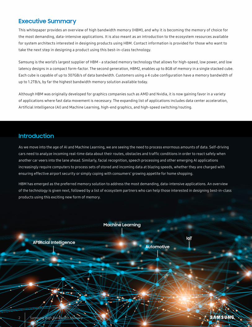
As we move into the age of AI and Machine Learning, we are seeing the need to process enormous amounts of data. Self-driving
cars need to analyze incoming real-time data about their routes, obstacles and traffic conditions in order to react safely when
another car veers into the lane ahead. Similarly, facial recognition, speech processing and other emerging AI applications
increasingly require computers to process sets of stored and incoming data at blazing speeds, whether they are charged with
ensuring effective airport security or simply coping with consumers’ growing appetite for home shopping.
HBM has emerged as the preferred memory solution to address the most demanding, data-intensive applications. An overview
of the technology is given next, followed by a list of ecosystem partners who can help those interested in designing best-in-class
products using this exciting new form of memory.
Artificial Intelligence
Machine Learning
Automotive
IoT
Executive Summary
2 Samsung High Bandwidth Memory
Si Interposer
PCB
Mother Board
Ch 0Ch 1Ch 2Ch 3Ch 4Ch 5Ch 6Ch 7
Logic
1024 I/Os
• 16 pseudo-channels (PC)
Buffer
Si Interposer
PCB
Mother Board
DRAM
PC2 PC3
PC0 PC1
Buffer DRAM
Logic Processor
1024 I/O
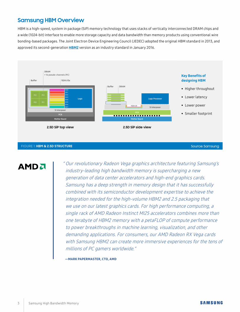
Samsung HBM Overview HBM is a high-speed, system in package (SiP) memory technology that uses stacks of vertically interconnected DRAM chips and
a wide (1024-bit) interface to enable more storage capacity and data bandwidth than memory products using conventional wire
bonding-based packages. The Joint Electron Device Engineering Council (JEDEC) adopted the original HBM standard in 2013, and
approved its second-generation HBM2 version as an industry standard in January 2016.
Key Benefits of designing HBM
• Higher throughout
• Lower latency
• Lower power
• Smaller footprint
3 Samsung High Bandwidth Memory
FIGURE 1: HBM & 2.5D STRUCTURE Source: Samsung
2.5D SiP side view2.5D SiP top view
“ Our revolutionary Radeon Vega graphics architecture featuring Samsung’s industry-leading high bandwidth memory is supercharging a new generation of data center accelerators and high-end graphics cards. Samsung has a deep strength in memory design that it has successfully combined with its semiconductor development expertise to achieve the integration needed for the high-volume HBM2 and 2.5 packaging that we use on our latest graphics cards. For high performance computing, a single rack of AMD Radeon Instinct MI25 accelerators combines more than one terabyte of HBM2 memory with a petaFLOP of compute performance to power breakthroughs in machine learning, visualization, and other demanding applications. For consumers, our AMD Radeon RX Vega cards with Samsung HBM2 can create more immersive experiences for the tens of millions of PC gamers worldwide.”
—MARK PAPERMASTER, CTO, AMD
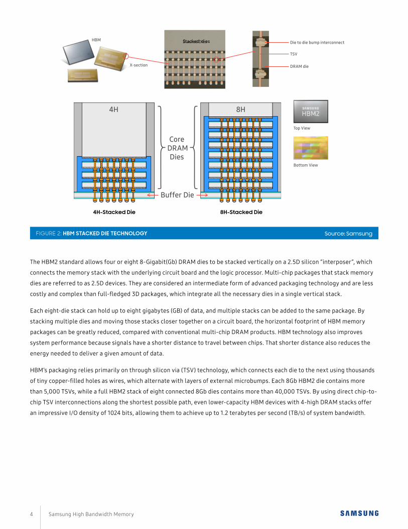
HBM
X-section
Die to die bump interconnect
Core DRAM
Dies
Buffer Die
TSV
DRAM die
Top View
Bottom View
4H 8H
Stacked Dies
4 Samsung High Bandwidth Memory
FIGURE 2: HBM STACKED DIE TECHNOLOGY Source: Samsung
4H-Stacked Die 8H-Stacked Die
The HBM2 standard allows four or eight 8-Gigabit(Gb) DRAM dies to be stacked vertically on a 2.5D silicon “interposer”, which
connects the memory stack with the underlying circuit board and the logic processor. Multi-chip packages that stack memory
dies are referred to as 2.5D devices. They are considered an intermediate form of advanced packaging technology and are less
costly and complex than full-fledged 3D packages, which integrate all the necessary dies in a single vertical stack.
Each eight-die stack can hold up to eight gigabytes (GB) of data, and multiple stacks can be added to the same package. By
stacking multiple dies and moving those stacks closer together on a circuit board, the horizontal footprint of HBM memory
packages can be greatly reduced, compared with conventional multi-chip DRAM products. HBM technology also improves
system performance because signals have a shorter distance to travel between chips. That shorter distance also reduces the
energy needed to deliver a given amount of data.
HBM’s packaging relies primarily on through silicon via (TSV) technology, which connects each die to the next using thousands
of tiny copper-filled holes as wires, which alternate with layers of external microbumps. Each 8Gb HBM2 die contains more
than 5,000 TSVs, while a full HBM2 stack of eight connected 8Gb dies contains more than 40,000 TSVs. By using direct chip-to-
chip TSV interconnections along the shortest possible path, even lower-capacity HBM devices with 4-high DRAM stacks offer
an impressive I/O density of 1024 bits, allowing them to achieve up to 1.2 terabytes per second (TB/s) of system bandwidth.
1750
1500
1250
1000
750
500
250
0
2015
Over 1 TB/s 1024 GB/s
1638 GB/s*
2016 2017 2018 2019 2020
(GB/
s)
HBM 2Cubes HBM 4Cubes GDDR 256bit GDDR 384bit
* = projection
5 Samsung High Bandwidth Memory
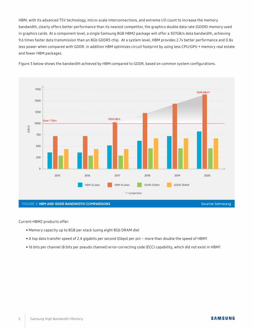
HBM, with its advanced TSV technology, micro-scale interconnections, and extreme I/O count to increase the memory
bandwidth, clearly offers better performance than its nearest competitor, the graphics double data rate (GDDR) memory used
in graphics cards. At a component level, a single Samsung 8GB HBM2 package will offer a 307GB/s data bandwidth, achieving
9.6 times faster data transmission than an 8Gb GDDR5 chip. At a system level, HBM provides 2.7x better performance and 0.8x
less power when compared with GDDR. In addition HBM optimizes circuit footprint by using less CPU/GPU + memory real estate
and fewer HBM packages.
Figure 3 below shows the bandwidth achieved by HBM compared to GDDR, based on common system configurations.
Current HBM2 products offer:
• Memory capacity up to 8GB per stack (using eight 8Gb DRAM die)
• A top data transfer speed of 2.4 gigabits per second (Gbps) per pin – more than double the speed of HBM1
• 16 bits per channel (8 bits per pseudo channel) error-correcting code (ECC) capability, which did not exist in HBM1
FIGURE 3: HBM AND GDDR BANDWIDTH COMPARISONS Source: Samsung
Samsung currently offers two generations of HBM2 -- Flarebolt with a pin speed of 2.0Gbps, and an even higher performing die
called Aquabolt that provides a 2.4 Gbps pin speed.
Today, Samsung is the world’s leading HBM supplier, and remains committed to expanding the technology roadmap to support
potential markets. Beyond HBM2, Samsung is actively looking into and leading the development of a third-generation
HBM3 standard, which is currently being drafted by JEDEC. While still being defined, the new HBM3 standard is expected to
accommodate more memory per die, more dies per stack and twice the maximum bandwidth of HBM2.
HBM2 is frequently used in high performance computing systems because of its lower power per bit. To implement HBM2
requires 2.5D PKG technology. Also, high performance systems require a companion logic chip to perform faster and consume
less power. So, the most advanced process technology should be used for logic chip manufacturing to lower the power. Thus,
Samsung Foundry delivers value by providing the following services to logic chip design companies:
• Advanced process chip manufacturing
• PKG service including 2.5D + HBM2
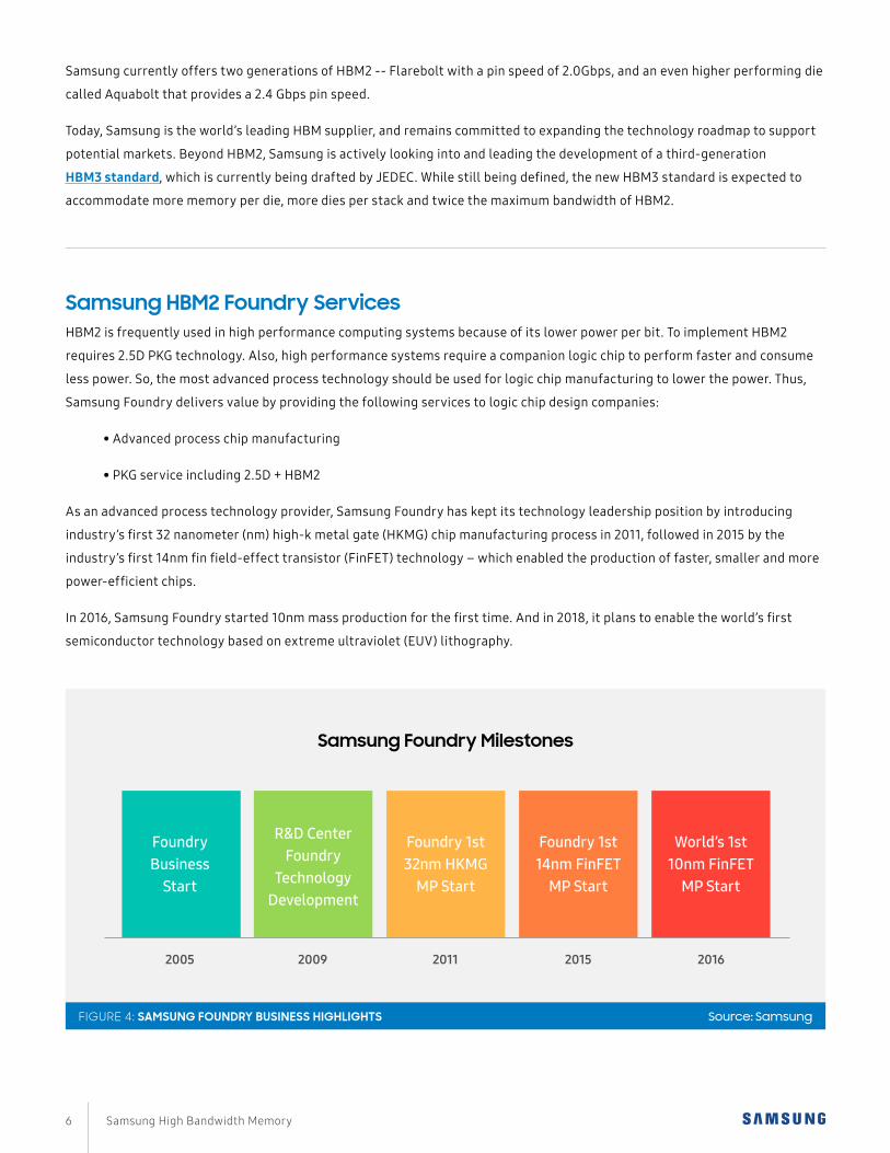
As an advanced process technology provider, Samsung Foundry has kept its technology leadership position by introducing
industry’s first 32 nanometer (nm) high-k metal gate (HKMG) chip manufacturing process in 2011, followed in 2015 by the
industry’s first 14nm fin field-effect transistor (FinFET) technology – which enabled the production of faster, smaller and more
power-efficient chips.
In 2016, Samsung Foundry started 10nm mass production for the first time. And in 2018, it plans to enable the world’s first
semiconductor technology based on extreme ultraviolet (EUV) lithography.
Samsung HBM2 Foundry Services
6 Samsung High Bandwidth Memory
2005 2009 2011 2015 2016
Foundry Business
Start
R&D Center Foundry
Technology Development
Foundry 1st 32nm HKMG
MP Start
Foundry 1st 14nm FinFET
MP Start
World’s 1st 10nm FinFET
MP Start
Samsung Foundry Milestones
FIGURE 4: SAMSUNG FOUNDRY BUSINESS HIGHLIGHTS Source: Samsung
5 Samsung High Bandwidth Memory6 Samsung High Bandwidth Memory
Samsung I-Cube, 2.5D Packaging and Turnkey Services
Samsung Foundry is now offering the company’s advanced logic process technology and packaging solutions to customers
designing a variety of mobile and high-performance computing (HPC) products. Working in close collaboration with several
leading logic chip designers and HBM interface and controller IP providers, Samsung has helped establish HBM2 technology as
the best available memory option for advanced graphics, network and server applications that require high capacity, bandwidth
and reliability, as well as outstanding energy- and space-efficiency. Samsung Foundry will shortly begin the volume production
of its new I-Cube 2.5D interposer chip, a turnkey solution for connecting HBM2 memory packages to processors or logic chips.
High-performance applications that have incorporated HBM technology can be demanding, especially when it comes to
maximizing the system performance of stacked DRAM wafers, high-density TSVs and tightly packed logic chips. Consequently,
HBM testability and supply chain management face additional complexities that are compounded by the rapid evolution of
technologies.
To effectively assist and navigate through these challenges, Samsung Foundry offers customers the complete turnkey service
including foundry, 2.5D packaging and HBM. This unique start-to finish production option is an advantage that only Samsung
Foundry can currently provide. And, Samsung Foundry will continue to provide end users with solutions that are effectively
optimized to meet the architectural requirements in new designs.
7 Samsung High Bandwidth Memory7 Samsung High Bandwidth Memory
Introducing a new and dramatically different memory technology like HBM typically requires an entire ecosystem of partners,
each of which has an important role to play. This kind of collaborative approach can speed product development by allowing
multiple companies to contribute specialized expertise in several different areas. Partners may also bring valuable supplier and
customer relationships, which can make it easier to establish an effective supply chain and to reassure end users considering
whether to implement the new technology in their own products.
Samsung’s current HBM2 ecosystem partners, and their main areas of expertise, include:
• Broadcom: HBM2 ASIC design and high-speed interface intellectual property (IP)
• eSilicon: FinFET ASIC, HBM2 Physical Layer (PHY) IP, 2.5D interposer design & differentiating IP
• Northwest Logic: HBM2 Controller IP
• Rambus: HBM2 Physical Layer (PHY) IP
• Synopsys: HBM2 PHY IP, Controller IP and Verification IP (VIP) for the system
• Cadence Design: VIP for the controller system
• ASE Group: Outsourced semiconductor assembly and test (OSAT)
Samsung’s HBM Ecosystem Partners
8 Samsung High Bandwidth Memory
Broadcom
The ASIC Products Division (APD) of San Jose, Calif.-based Broadcom Ltd.
www.broadcom.com has a long history of providing innovative application-specific integrated circuit (ASIC) solutions for
advanced networking and high-performance computing applications. APD offers a comprehensive technology platform in
advanced process nodes along with a broad range of ASIC design implementation services. APD enables its customers to
differentiate in the market place with cutting edge, early adopter custom silicon.
APD has already landed a large number of 2.5D ASIC design wins across multiple process nodes, and its first HBM ASIC started
volume production in 2017.
Besides its ASIC design skills, Broadcom’s APD offers two key pieces of silicon-proven interface technology to the growing
Samsung HBM technology ecosystem: HBM2 physical layer (PHY) IP, and high-speed serializer/deserializer (SerDes) IP. It also
offers expertise in supply chain management, power integrity and signal integrity capability, and packaging design.
APD’s HBM ASIC devices, based on 7nm process technology, offer the high bandwidth and channel density necessary to support
a variety of advanced applications, including:
• Artificial intelligence and deep learning
• High-performance computing
• Switching and routing
Successfully implementing 2.5D ASIC technology requires a large investment and steep learning curve that only a few
companies have the ability to support. Broadcom has made the necessary investment to expand its 2.5D offering to provide
unprecedented performance and value in the 7nm process node.
ASIC and IP Design
“ While HBM technology offers tremendous performance advantages, it also poses significant design and manufacturing challenges. By working closely with Samsung and developing a broad portfolio of supporting IP and 2.5D package design and manufacturing capabilities, we have suc-cessfully overcome those challenges, resulting in a lower-risk path to volume production for our customers.”
—HUGH DURDAN, VICE PRESIDENT OF STRATEGY AND PRODUCTS, ESILICON
eSilicon
San Jose, Calif.-based eSilicon Corp. www.esilicon.com designs and manufactures ASICs and the differentiating IP that enables
high-performance networking, computing, AI/deep learning and 5G infrastructure products. It has completed successful tapeouts
of advanced ASIC and 2.5D designs for these applications, and is currently delivering one of the industry’s first HBM deep learning
ASICs for a tier-one customer.
eSilicon has been developing 2.5D systems since 2011. To ensure customer success in volume manufacturing, eSilicon includes the
following services in its ASIC engagements:
• Interposer and package design and routing • Signal and power integrity analysis
• Design for manufacturability • Thermal integrity and warpage analysis
As a leader in 2.5D systems, it acts as a single production source for the acquisition and assignment of all die in the package, as well
as assembly, test and delivery of the final tested, yielded device. It supports multiple packaging, interposer and FinFET wafer fab
partners, and helps each customer pick the right technology for their design.
eSilicon’s FinFET IP portfolio includes high-speed SerDes, multi-port memories, fast caches and register files, a family of ternary
content addressable memories (TCAMs) and HBM2 PHYs. Because eSilicon uses all of this IP in its ASIC engagements, it understands
what it takes to successfully design a complex device incorporating the IP, unlike traditional IP companies who design but never use
their IP products. It also maintains a large staff of IP designers to customize IP for unique customer applications and needs.
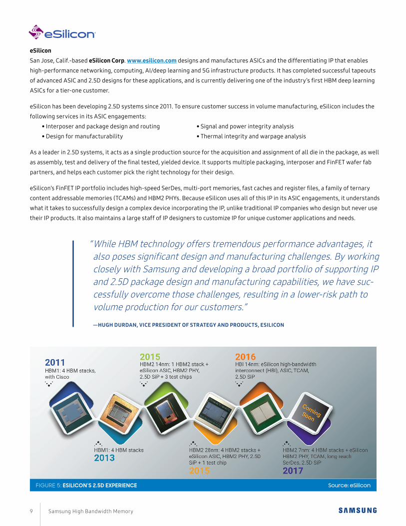
eSilicon’s 2.5D Experience
9 Samsung High Bandwidth Memory
FIGURE 5: ESILICON’S 2.5D EXPERIENCE Source: eSilicon
AXI Interface
OCP Interface
Mul
ti-P
ort F
ront
-End
Reorder
Memory TestMem Test Analyzer
HBM2 Controller
HBM2 PHY HBM2Memory
RMW
ECC
Controller/PHY IP
Northwest Logic (www.nwlogic.com), located in Beaverton, Oregon, offers the market-leading HBM2 Controller IP with the
following key advantages:
• Fully silicon proven in 17 customer designs and 7 test chips thus far. 100% success rate for all tapeouts.
• Supports all HBM2 data rates (2.0, and 2.4Gbit/s/pin and beyond) and stack configurations (four die, eight die).
• Highly configurable to minimize size and power and maximize performance and ease of use.
• Full featured including optional add-on cores, comprehensive memory test and high reliability features.
• Provides maximum memory efficiency over a wide range of traffic scenarios.
• Delivered fully integrated and verified with a wide range of customer-selected, silicon-proven HBM2 PHYs.
NEC used Northwest Logic’s HBM2 Controller IP in its new line of SX-Aurora TSUBASA high-performance supercomputers. A key
component of this product is the 8 core Vector Engine processor which connects to six HBM2 modules. The use of HBM2 provided
a 5x performance per core improvement over the previous DDR3-based processor. It also helped provide a 5x per watt and 10x per
square meter of floor space improvement over NEC’s previous generation product. NEC stated, “We are pleased we were able to
meet our performance goals with an efficient gate utilization using Northwest Logic’s HBM2 Controller IP.”
“ Our collaboration with Samsung ensures that our customers achieve the highest possible system performance when using the combination of Northwest Logic’s HBM2 Controller IP and Samsung’s HBM2 devices.”
—BRIAN DAELLENBACH, PRESIDENT, NORTHWEST LOGIC
10 Samsung High Bandwidth Memory
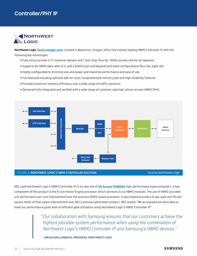
FIGURE 6: NORTHWEST LOGIC’S HBM2 CONTROLLER SOLUTION Source: Northwest Logic
Rambus
The Memory and Interfaces Division of Sunnyvale, Calif.-based Rambus Inc.
www.rambus.com develops products and services that solve the power, performance, capacity and interoperability challenges
of the communications and data center computing markets.
Rambus has extensive experience with complex 2.5D and 3D system design, and its HBM Gen2 PHY interface IP is fully
standards-compliant, supporting data rates up to 2,000 Mbps per data pin, for a total bandwidth of 256 GB/s. The interface
features 8 independent channels, each containing 128 bits for a total data width of 1024 bits, and it supports vertical stacks
of 2, 4 or 8 DRAM dies. It also supports multiple PHYs, allowing chip designers to customize the interface by increasing or
decreasing the number of channels.
To ensure easy implementation and improved design flexibility, Rambus performs complete signal- and power-integrity
analysis on the entire 2.5D system to ensure that all signal, power and thermal requirements are met. Rambus also has
announced validated interoperability between its HBM2 PHY and Northwest Logics’ HBM2 Controller IP. Along with Samsung’s
DRAM and interposer chips, the companies’ offer a complete, silicon-proven and verified HBM2 solution that can be configured
to exact customer requirements.
Time (in ps)
Volt
age
(in m
V)
“ As a provider of high-speed and innovative IP, Rambus is pleased to continue our work with a leading foundry provider like Samsung. Collaborating with Samsung ensures high performance IP and high quality solutions to our end customers.”
— LUC SERAPHIN, SENIOR VICE PRESIDENT AND GENERAL MANAGER OF MEMORY AND INTERFACES DIVISION, RAMBUS
11 Samsung High Bandwidth Memory
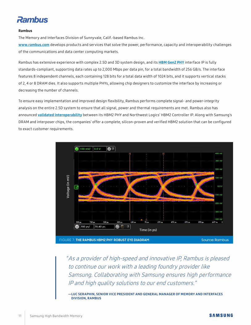
FIGURE 7: THE RAMBUS HBM2 PHY ROBUST EYE DIAGRAM Source: Rambus
Synopsys
Besides being the world’s leading Electronic Design Automation (EDA) vendor, Mountain View, Calif.-based Synopsys Inc.
www.synopsys.com is also a leading supplier of DDR and HBM semiconductor interface IP. Its HBM PHY interface IP was used
in Advanced Micro Devices’ (AMD’s) Fiji GPUs – the first graphics processors to feature high bandwidth memory – in 2015.
Synopsys’ DesignWare HBM2 PHY was also the first HBM2 PHY IP to reach volume production as part of AMD’s Vega GPUs.
Available in 16nm, 14nm, 12nm and 7nm technologies as part of Synopsys’ extensive DesignWare IP portfolio, Synopsys’ HBM2
PHY IP is optimized for high performance, low latency, low area use, low power and ease of integration. The DesignWare HBM2
PHY is delivered in GDSII database format as a set of hard macrocells that can be assembled into a complete 512-bit or 1024-bit
HBM2 PHY supporting 2, 4 or 8-high HBM2 stacks.
Synopsys offers a complete HBM2 interface solution, including PHY, controller, and verification IP. Its DesignWare HBM2
controller is built from the industry leading DesignWare Enhanced Universal DDR Memory Controller, and features high
bandwidth, as well as low area use and low latency. It comes with verification IP that complies with the HBM and HBM2 JEDEC
specifications and provides protocol, methodology, verification and productivity features including built-in protocol checks,
coverage and verification plans, and Verdi protocol-aware debug and performance analysis, enabling users to rapidly verify
HBM-based designs.
Synopsys’ HBM2 IP is available with a variety of service options including PHY hardening, 2.5D interposer design assistance and
subsystems and signal integrity services.
12 Samsung High Bandwidth Memory
“ We selected Synopsys’ DesignWare HBM2 IP solution to take full advantage of the bandwidth and power efficiency of the 16GB of HBM2 memory in our Radeon™ Vega Frontier Edition graphics cards. Synopsys’ deep expertise in memory interfaces enabled us to successfully integrate HBM2 IP into the ‘Vega’ GPU architecture and achieve aggressive power and memory bandwidth targets to serve Machine Learning and advanced graphics applications.”
—JOE MACRI, CORPORATE VP AND PRODUCT CTO, AMD
12 Samsung High Bandwidth Memory
Cadence Design
Cadence provides Verification IP components for the HBM ecosystem. This verification IP (VIP) provides support for the JEDEC®
High-Bandwidth Memory (HBM) DRAM device standard, from pre 1.0 to current 2.0x versions. It provides a mature, highly
capable compliance verification solution that supports simulation, formal analysis, and hardware acceleration platforms,
making it applicable to intellectual property (IP), system-on-chip (SoC), and system-level verification. The HBM VIP models
a single channel of HBM DRAM; this model can be replicated for multiple channels and multiple ranks. The model runs on all
leading simulators, and leverages the industry-standard Cadence Memory Model core architecture, interface, and use model.
Introduction
With a proven track record spanning over three decades, ASE, the OSAT (Outsourced Services in Assembly & Test) market
leader, continues its tradition of manufacturing expertise through orchestrated collaboration with customers, suppliers and
partners, alike. Alongside a broad portfolio of established technologies, ASE is delivering innovative advanced packaging,
System-in-Package and MEMS solutions. Dedicated teams are innovating across technology and ecosystem to facilitate
the timely manufacture of devices and systems enabling higher performance, lower power, greater speed, and increased
bandwidth. With applications spanning artificial intelligence, automotive, IoT, mobile, and high performance computing, ASE is
dedicated to working within industry partnerships for the ultimate benefit of mankind.
ASE: Assembly & Test
2.5D technology is at the forefront of advanced packaging technologies, enabling unprecedented achievement in interconnect
density, power and performance. Assembly and test play a pivotal role. Over the last decade, ASE has partnered across the
ecosystem to carry out extensive work from initial proof of concept to technology feasibility to product development to
production ramp and ultimately high volume production. In May 2015, ASE became the first OSAT in production for 2.5D IC with
HBM devices. As of December 2017, ASE’s 2.5D high volume production had achieved over 3,000 interposers and over 150K units.
HBM is essentially a 3D IC, featuring stacked die with through silicon vias and microbumps for die-to-die interconnect,
while 2.5D refers to die stacked packaging technologies that use interposers to achieve the highest level of die-to-die
interconnectivity currently available. ASIC and HBM connection is achieved using silicon interposer enabling the HBM to
produce high bandwidth while reducing 90% of the data transfer distance. The improved die-to-die proximity enables
extremely low latency and power efficiency. Further, the 2.5D platform enables significant dimensional reduction between
interconnects: a microbump size is 8000 times smaller than a solder ball and is also 125 times smaller than a C4 bump.
Currently, a silicon interposer is approximately 100 μm in thickness, while allowing more than 100K interconnects for the ASIC
and HBM connection. 2.5D technologies are developed to meet requirements for high performance computing, such as high
speed transmission, high bandwidth, and lower power consumption.
13 Samsung High Bandwidth Memory13 Samsung High Bandwidth Memory
Outsourced assembly and test (OSAT)
The ASE 2.5D Advantage
The sheer complexity of 2.5D technology presents many challenges that must be overcome during the manufacturing process.
HBM is currently shipped to ASE in tape and reel form, requiring incoming inspection, assembly, test and outgoing inspection.
Alignment accuracy is critical because X-Ray cannot be used to carry out inspection. The assembly process needs to be highly
robust to mitigate any risk of costly damage to the HBM. Both incoming and outgoing inspection must be well aligned. Every
process and subsequent yield are likewise critical.
The microbumps are minuscule therefore warpage control must be closely monitored, as must particle control, given high
sensitivity to any foreign material during the assembly process.
Partnership with ASE can enhance overall 2.5D quality. The incoming and outgoing inspection methodology and criteria ASE
has implemented meets stringent requirements for reliability and performance. ASE provides customers with flexible process
flows to meet their needs. Specifically, HBM-last assembly process has been developed such that any loss prior to HBM attach
will not sacrifice the high value HBM. ASE can also provide molding-type 2.5D solutions to customers. With proven high quality
process capabilities as required by 2.5D packaging, ASE can be considered a strong and reliable partner to bring such complex
and powerful products to market.
14 Samsung High Bandwidth Memory14 Samsung High Bandwidth Memory
“ As ASE keeps pace with the changing electronics landscape and related System in Package (SiP) technology requirements, we need to be in lockstep with all partners within our ecosystem. The evolution of the partnership with Samsung is a reflection of the steadfast commitment to the advancement of HBM innovation and application, which will ultimately enable the next wave of high bandwidth, power efficiency and space savings in high performance applications and products. Packaging and test play a pivotal role, particularly given the increasing complexity of HBM, and ASE is scaling its SiP technology and collaboration for 2018 and well beyond.”
—DR. CP HUNG, VICE PRESIDENT OF CORPORATE RESEARCH & DEVELOPMENT, ASE GROUP
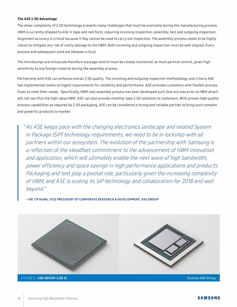
FIGURE 8 : ASE GROUP: 2.5D IC Source: ASE Group
Looking Ahead: An HBM Roadmap to the Future
In the coming era of self-driving cars, real-time speech processing and continuous Machine Learning, ever-more powerful
technology will be needed to handle the unprecedented volumes of data these applications will generate. Samsung’s High
Bandwidth Memory (HBM) has the exceptional capacity, bandwidth, performance and power efficiency needed to handle
today’s—and tomorrow’s—toughest computing tasks.
HBM is designed to easily outperform competing memory solutions such as GDDR5, while Samsung’s ecosystem of world-
class technology partners is eminently qualified to provide all the additional support and services you’ll need to take your
project from initial design to final manufacturing and test.
The market success of Nvidia’s Tesla P100 and V100, as well as AMD’s Vega, demonstrate both the mass market appeal and
ecosystem readiness of HBM2.
Whether it’s eSilicon’s high-performance deep learning ASICs, Broadcom’s 2.5D ASIC design wins, Synopsys’ easily
integrated DesignWare HBM2 PHYs, Northwest Logic’s best-selling HBM2 controllers or the unrivaled capabilities of ASE,
the world’s largest outsourced semiconductor assembly and test provider, our lineup of technology assets, customer-
service skills and demonstrated industry leadership is second to none.
Backed by Samsung’s commitment to continuous innovation and collaboration, our long-term HBM roadmap is as relevant
to today’s emerging applications as it will be to tomorrow’s leading markets. Samsung is building the memory technology of
the future and would like to invite you to be part of it.
Copyright 2018 Samsung Electronics, Co. Ltd. All Rights Reserved. All brand, product, service names and logos are trademarks and/or registered trademarks of their respective owners and are hereby recognized and acknowledged. Specifications and designs are subject to change without notice. All data were deemed correct at time of creation. Samsung is not liable for errors or omissions.
15 Samsung High Bandwidth Memory