Embed Size (px)
Citation preview
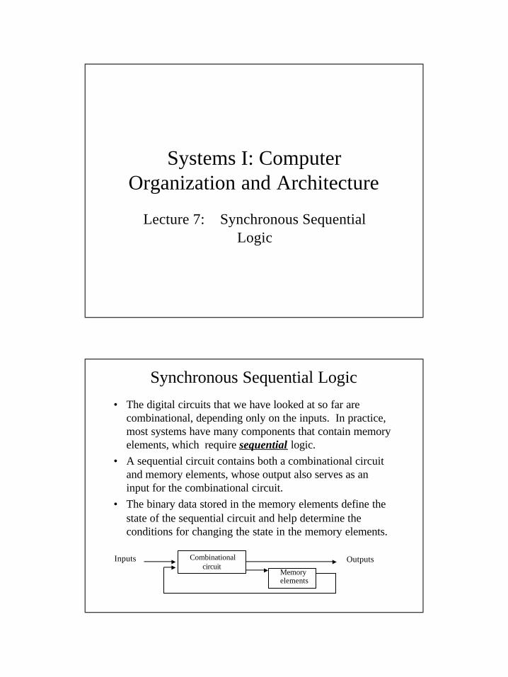
Systems I: Computer Organization and Architecture
Lecture 7: Synchronous Sequential Logic
Synchronous Sequential Logic• The digital circuits that we have looked at so far are
combinational, depending only on the inputs. In practice, most systems have many components that contain memory elements, which require sequential logic.
• A sequential circuit contains both a combinational circuit and memory elements, whose output also serves as an input for the combinational circuit.
• The binary data stored in the memory elements define the state of the sequential circuit and help determine the conditions for changing the state in the memory elements.
Combinationalcircuit
Memoryelements
Inputs Outputs
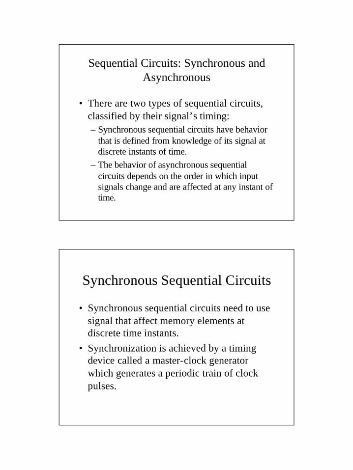
Sequential Circuits: Synchronous and Asynchronous
• There are two types of sequential circuits, classified by their signal’s timing:– Synchronous sequential circuits have behavior
that is defined from knowledge of its signal at discrete instants of time.
– The behavior of asynchronous sequential circuits depends on the order in which input signals change and are affected at any instant of time.
Synchronous Sequential Circuits
• Synchronous sequential circuits need to use signal that affect memory elements at discrete time instants.
• Synchronization is achieved by a timing device called a master-clock generator which generates a periodic train of clock pulses.
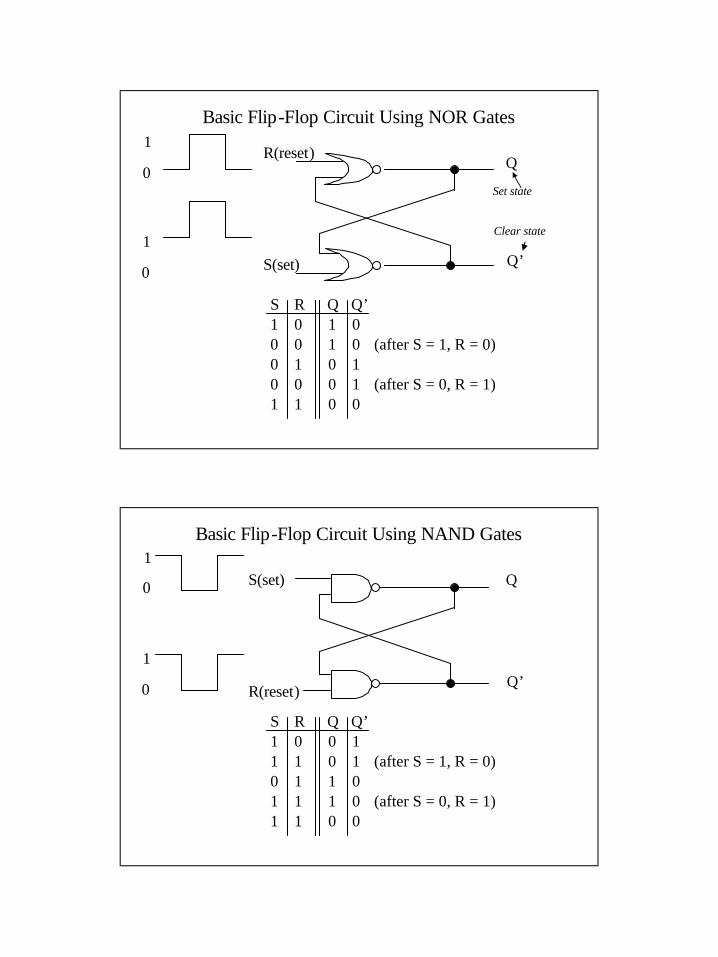
Basic Flip-Flop Circuit Using NOR Gates
QR(reset)
S(set)0
1
0
1
Q’S QR1 1
10 0
0000 1 0 1
0 1000011
(after S = 1, R = 0)
(after S = 0, R = 1)
Set state
Clear state
Q’
Basic Flip-Flop Circuit Using NAND Gates
Q
0
1
Q’S QR1 0
00 1
1110 1 1 0
1 0110011
(after S = 1, R = 0)
(after S = 0, R = 1)
0
1S(set)
R(reset)Q’
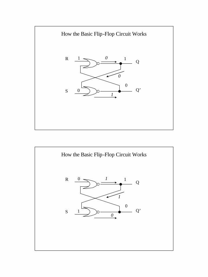
How the Basic Flip-Flop Circuit Works
QR
S Q’0
1
1
0
0
0
1
How the Basic Flip-Flop Circuit Works
QR
S Q’1
0
0
1
1 1
0
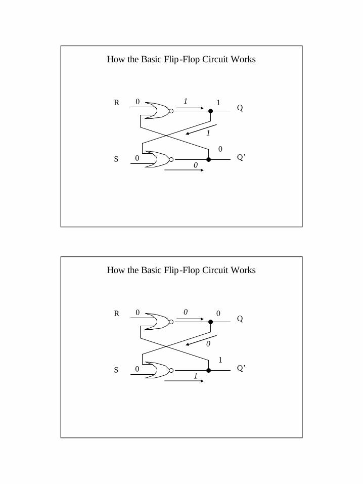
How the Basic Flip-Flop Circuit Works
QR
S Q’0
0
0
1
1 1
0
How the Basic Flip-Flop Circuit Works
QR
S Q’0
0
1
0
0 0
1
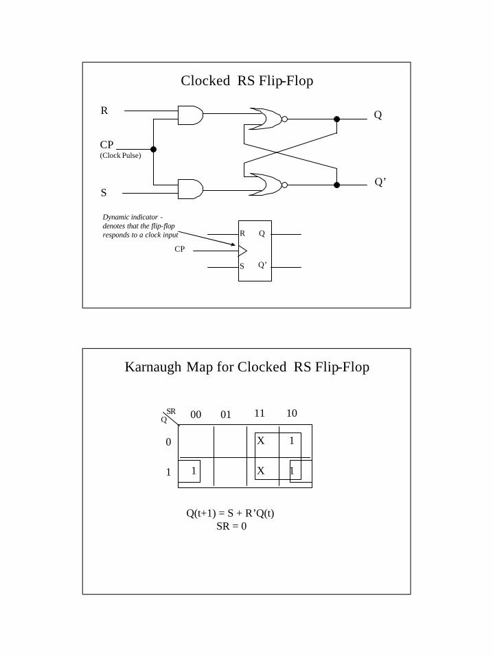
Clocked RS Flip-Flop
Q
Q’
R
S
CP(Clock Pulse)
CP
R
S
Q
Q’
Dynamic indicator -denotes that the flip-flopresponds to a clock input
Karnaugh Map for Clocked RS Flip-Flop
SRQ
0
1
00 01 11 10
X
X
1
11
Q(t+1) = S + R’Q(t) SR = 0
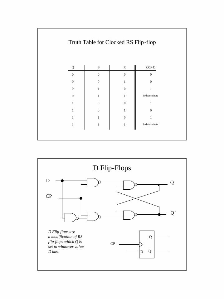
Truth Table for Clocked RS Flip-flop
Q S R Q(t+1)
0 0 0 0
0 0 1 0
0 1 0 1
0 1 1 Indeterminate
1 0 0 1
1 0 1 0
1 1 0 1
1 1 1 Indeterminate
D Flip-Flops
Q
Q’
D
CP
CP
D
Q
Q’
D Flip-flops area modification of RS flip-flops which Q isset to whatever valueD has.
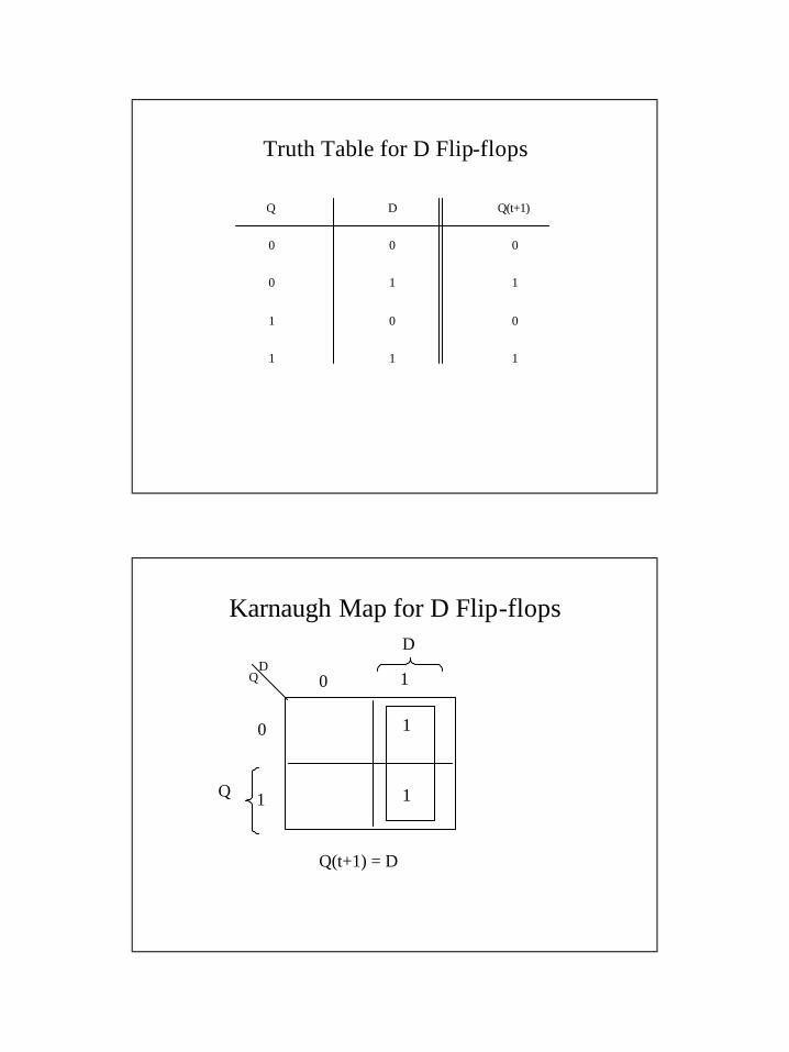
Truth Table for D Flip-flops
Q D Q(t+1)
0 0 0
0 1 1
1 0 0
1 1 1
Karnaugh Map for D Flip-flops
0
0
1
1
1
1
QD
Q
D
Q(t+1) = D
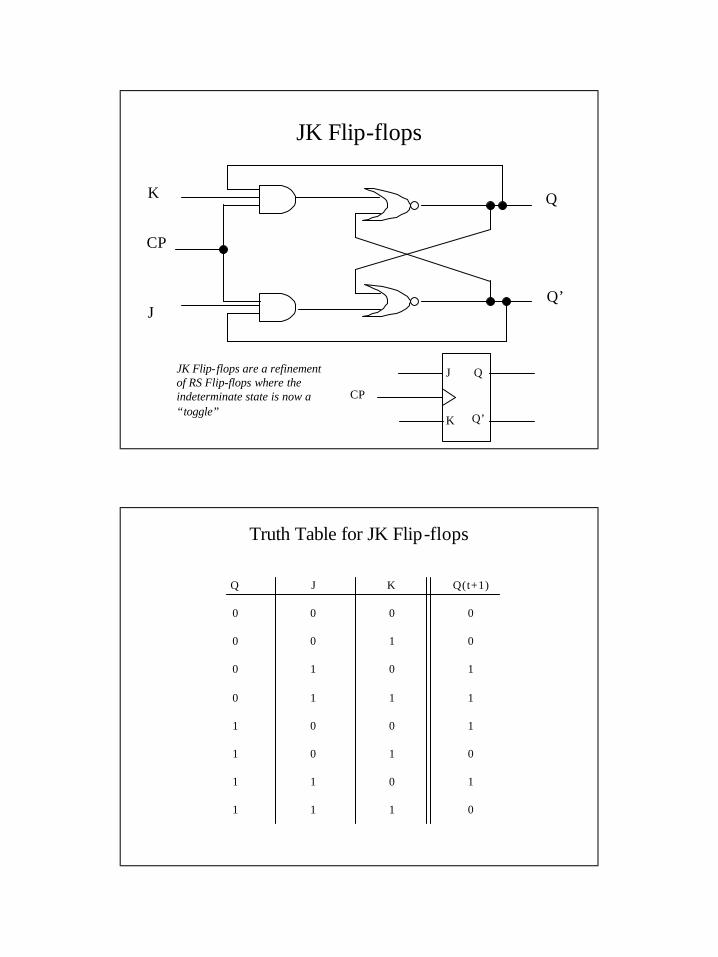
JK Flip-flops
Q
Q’
K
J
CP
JK Flip-flops are a refinement of RS Flip-flops where theindeterminate state is now a “toggle”
CP
J
K
Q
Q’
Truth Table for JK Flip-flops
Q J K Q(t+1)
0 0 0 0
0 0 1 0
0 1 0 1
0 1 1 1
1 0 0 1
1 0 1 0
1 1 0 1
1 1 1 0
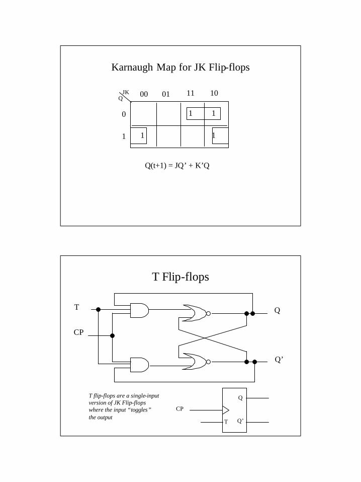
Karnaugh Map for JK Flip-flops
JKQ
0
1
00 01 11 10
1 1
11
Q(t+1) = JQ’ + K’Q
T Flip-flops
Q
Q’
T
CP
CP
T
Q
Q’
T flip-flops are a single-inputversion of JK Flip-flops where the input “toggles”the output
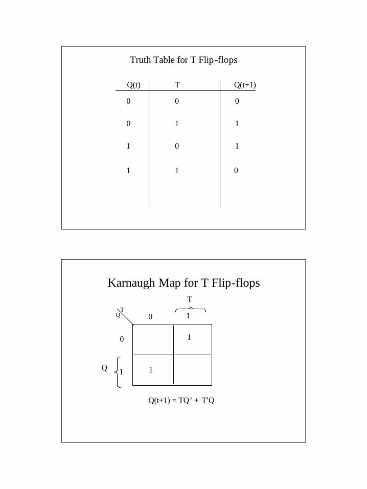
Truth Table for T Flip-flops
Q(t) Q(t+1)T
0 0
0
1
1
1
0
1
0 1
1 0
Karnaugh Map for T Flip-flops
0
0
1
1
1
1
QT
Q
T
Q(t+1) = TQ’ + T’Q
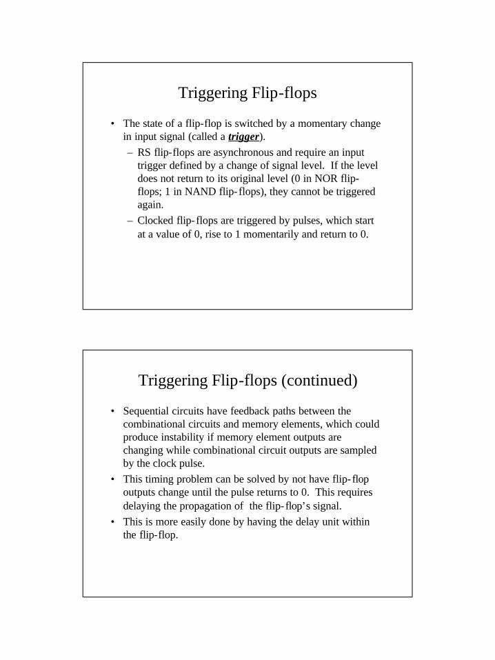
Triggering Flip-flops
• The state of a flip-flop is switched by a momentary change in input signal (called a trigger).– RS flip-flops are asynchronous and require an input
trigger defined by a change of signal level. If the level does not return to its original level (0 in NOR flip-flops; 1 in NAND flip-flops), they cannot be triggered again.
– Clocked flip-flops are triggered by pulses, which start at a value of 0, rise to 1 momentarily and return to 0.
Triggering Flip-flops (continued)
• Sequential circuits have feedback paths between the combinational circuits and memory elements, which could produce instability if memory element outputs are changing while combinational circuit outputs are sampled by the clock pulse.
• This timing problem can be solved by not have flip-flop outputs change until the pulse returns to 0. This requires delaying the propagation of the flip-flop’s signal.
• This is more easily done by having the delay unit within the flip-flop.
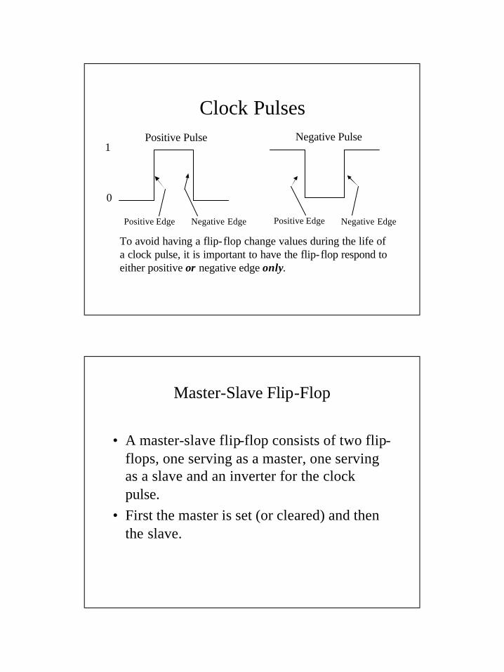
Clock PulsesPositive Pulse
Positive Edge Negative Edge
Negative Pulse
Positive Edge Negative Edge
1
0
To avoid having a flip-flop change values during the life ofa clock pulse, it is important to have the flip-flop respond to either positive or negative edge only.
Master-Slave Flip-Flop
• A master-slave flip-flop consists of two flip-flops, one serving as a master, one serving as a slave and an inverter for the clock pulse.
• First the master is set (or cleared) and then the slave.
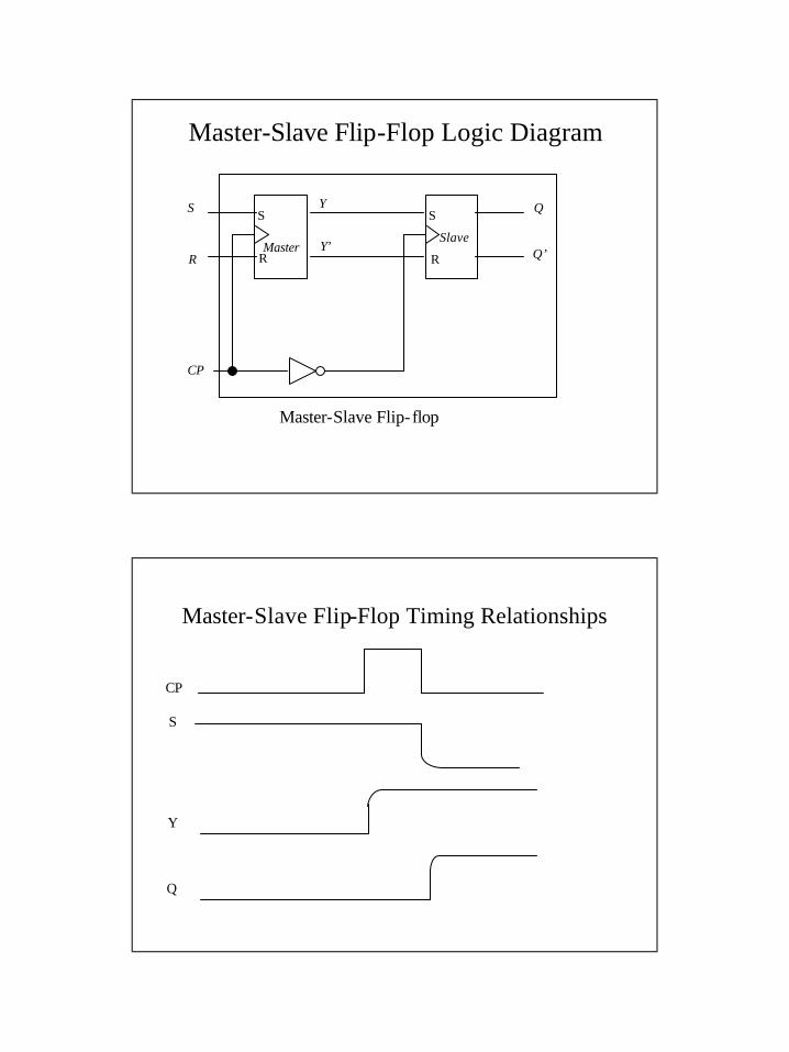
Master-Slave Flip-Flop Logic Diagram
S
RMaster
S
R
Slave
Y
Y’
Q
Q’
CP
S
R
Master-Slave Flip-flop
Master-Slave Flip-Flop Timing Relationships
CP
S
Y
Q
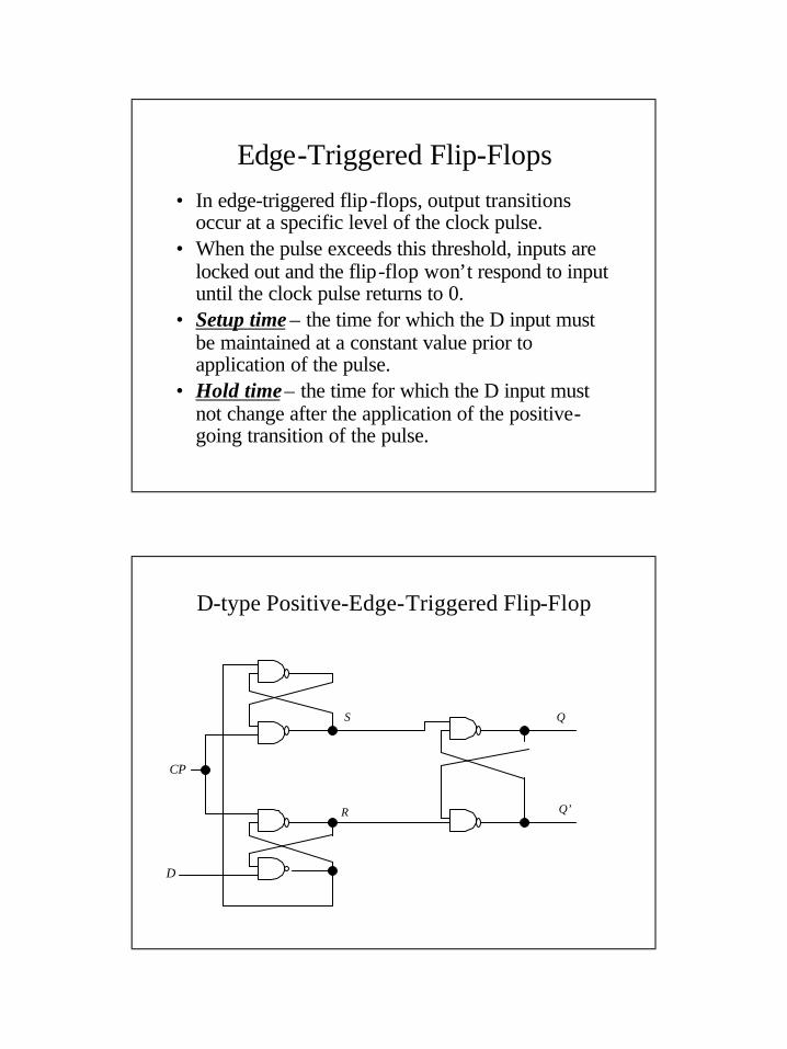
Edge-Triggered Flip-Flops• In edge-triggered flip-flops, output transitions
occur at a specific level of the clock pulse.• When the pulse exceeds this threshold, inputs are
locked out and the flip-flop won’t respond to input until the clock pulse returns to 0.
• Setup time – the time for which the D input must be maintained at a constant value prior to application of the pulse.
• Hold time– the time for which the D input must not change after the application of the positive-going transition of the pulse.
D-type Positive-Edge-Triggered Flip-Flop
S
R
Q
Q’
CP
D
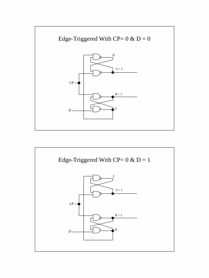
Edge-Triggered With CP= 0 & D = 0
S = 1
R = 1
CP
D
0
1
Edge-Triggered With CP= 0 & D = 1
S = 1
R = 1
CP
D
1
0
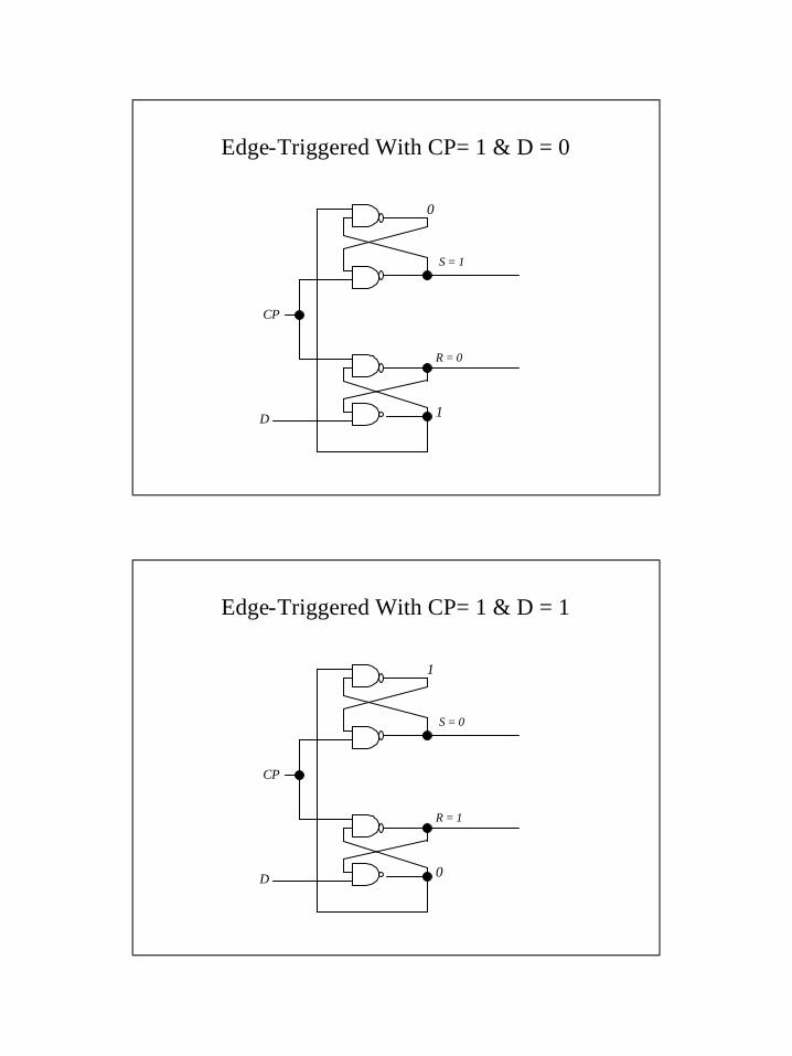
Edge-Triggered With CP= 1 & D = 0
S = 1
R = 0
CP
D
0
1
Edge-Triggered With CP= 1 & D = 1
S = 0
R = 1
CP
D
1
0
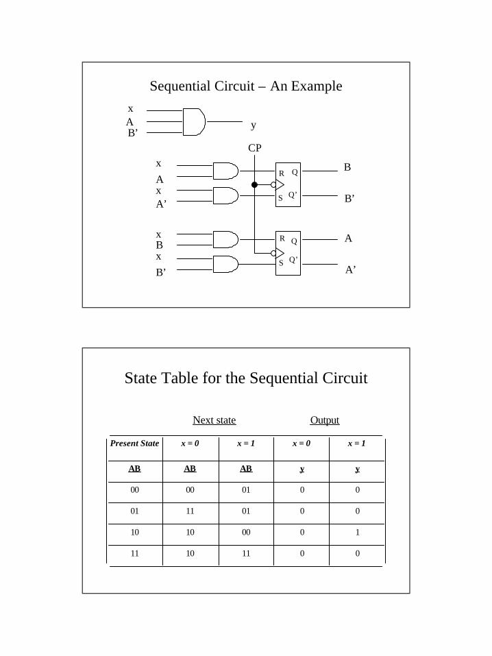
Sequential Circuit – An Example
AB’
xy
CP
B
B’
A
A’
x
x
x
x
A
A’
B’
B
R
S
Q
Q’
R
S Q’
Q
State Table for the Sequential Circuit
00111011
10001010
00011101
00010000
yyABABAB
x = 1x = 0x = 1x = 0Present State
Next state Output
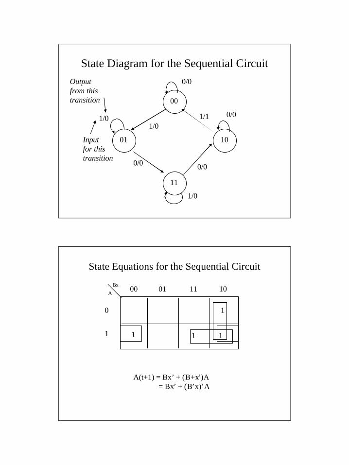
State Diagram for the Sequential Circuit
00
01 10
11
0/0
1/0
Inputfor thistransition
Outputfrom thistransition
1/01/1
0/00/0
0/0
1/0
State Equations for the Sequential Circuit
Bx
A00 01 11 10
0
1 1 1 1
1
A(t+1) = Bx’ + (B+x’)A= Bx’ + (B’x)’A
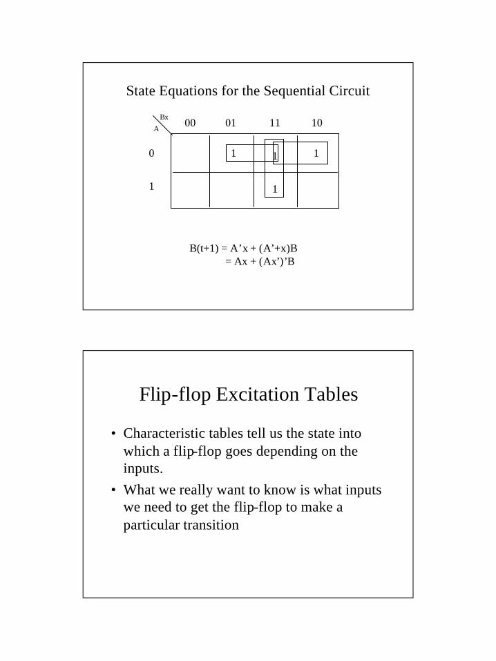
State Equations for the Sequential Circuit
Bx
A00 01 11 10
0
1
1
1
1 1
B(t+1) = A’x + (A’+x)B= Ax + (Ax’)’B
Flip-flop Excitation Tables
• Characteristic tables tell us the state into which a flip-flop goes depending on the inputs.
• What we really want to know is what inputs we need to get the flip-flop to make a particular transition
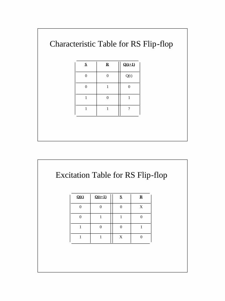
Characteristic Table for RS Flip-flop
?11
101
010
Q(t)00
Q(t+1)RS
Excitation Table for RS Flip-flop
0X11
1001
0110
X000
RSQ(t+1)Q(t)
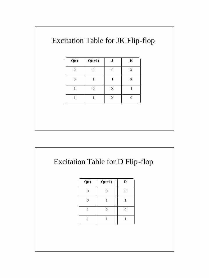
Excitation Table for JK Flip-flop
0X11
1X01
X110
X000
KJQ(t+1)Q(t)
Excitation Table for D Flip-flop
111
001
110
000
DQ(t+1)Q(t)
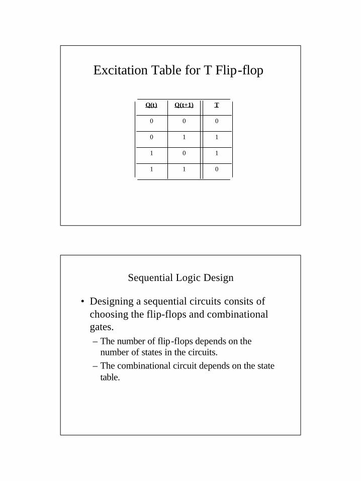
Excitation Table for T Flip-flop
011
101
110
000
TQ(t+1)Q(t)
Sequential Logic Design
• Designing a sequential circuits consits of choosing the flip-flops and combinational gates.– The number of flip-flops depends on the
number of states in the circuits.– The combinational circuit depends on the state
table.
Sequential Logic Design Procedure
• The procedure is summarized by these steps:1. The word description of the circuit behavior is states,
accompanied by a state diagram, timing diagram or other pertinent data.
2. Obtain the state table from the given information about the circuit.
3. The number of states may be reduced if the sequential circuit can be characterized by input-output relationships independent of the number of states.
4. Assign binary values to each state if the state table obtained in step 2 or 3 contains letter symbols.
Sequential Logic Design Procedure (continued)
5.Determine the number of flip-flops needed and assign a letter symbol to each
6.Choose the type of flip-flop to be used.7.From the state table, derive the circuit
excitation and output table.8.Using the map or any other simplification
method, derive the circuit output function and the flip-flop input functions.
9.Draw the logic diagram.
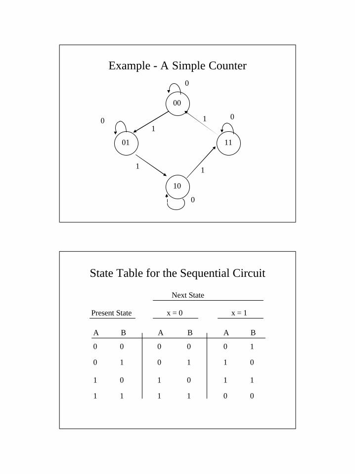
Example - A Simple Counter
00
01 11
10
0
01
1
11
0
0
State Table for the Sequential Circuit
Present State x = 1x = 0
Next State
A A AB B B
0 00 0 0 1
1 00 1 1 0
0 11 0 1 1
1 11 1 0 0
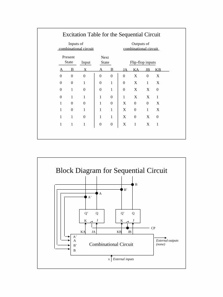
Excitation Table for the Sequential Circuit
Present State
Next State
A B
00
00
10
10
01
01
11
11
Input
x0
1
0
1
0
1
0
1
A B
00
10
10
01
01
11
11
00
Flip-flop inputs
X0
X0
X0
X1
0X
0X
0X
1X
0
1
X
X
0
1
X
X
X
X
0
1
X
X
0
1
JB KBJA KA
Inputs of combinational circuit
Outputs of combinational circuit
Block Diagram for Sequential Circuit
Combinational Circuit
K J
Q’ Q
KA JA
K J
Q’ Q
KB JBCP
x External inputs
External outputs(none)
A’A
B’
B
BB’AA’
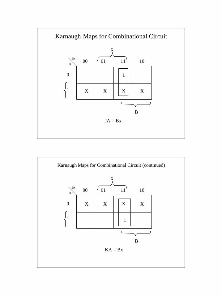
Karnaugh Maps for Combinational Circuit
Bx
A00 01 11 10
0
1 X X X
1
X
JA = Bx
x
B
Karnaugh Maps for Combinational Circuit (continued)
Bx
A00 01 11 10
0
1
X X X
1
X
KA = Bx
x
B
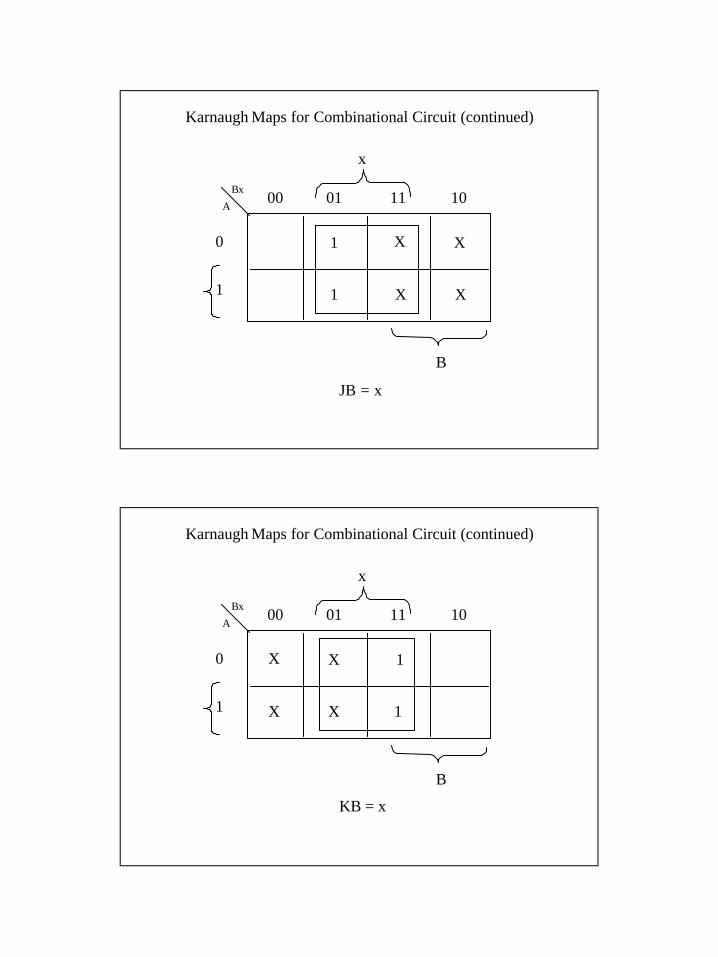
Karnaugh Maps for Combinational Circuit (continued)
Bx
A00 01 11 10
0
1 X
X X
1 X
JB = x
x
B
1
Karnaugh Maps for Combinational Circuit (continued)
Bx
A00 01 11 10
0
1 X
X X
1X
KB = x
x
B
1
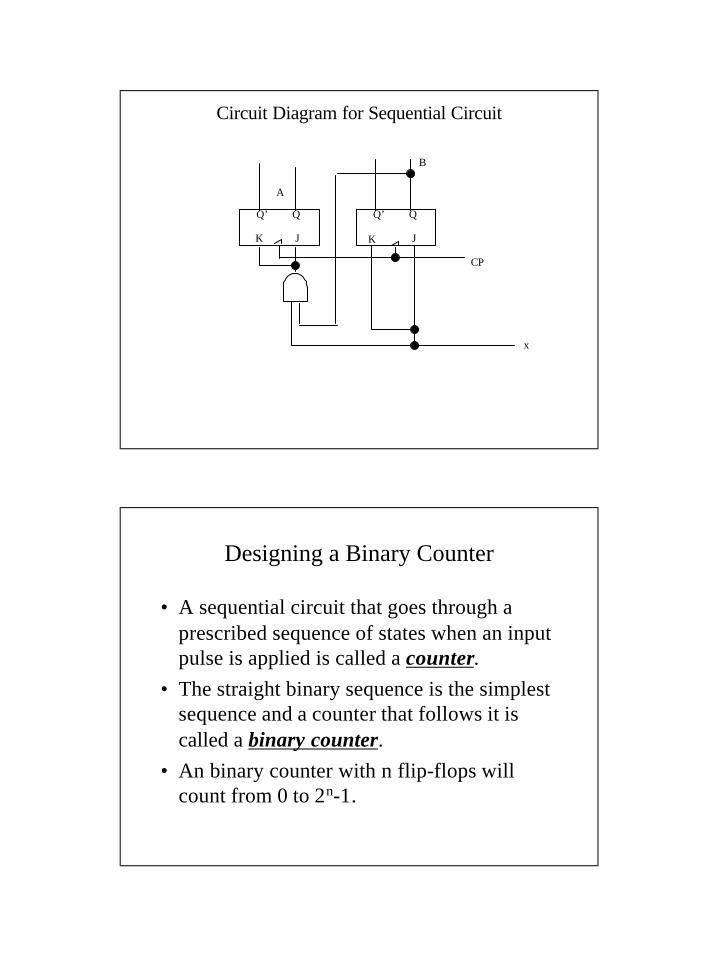
Circuit Diagram for Sequential Circuit
K J
Q’ Q
K J
Q’ Q
CP
A
B
x
Designing a Binary Counter
• A sequential circuit that goes through a prescribed sequence of states when an input pulse is applied is called a counter.
• The straight binary sequence is the simplest sequence and a counter that follows it is called a binary counter.
• An binary counter with n flip-flops will count from 0 to 2n-1.
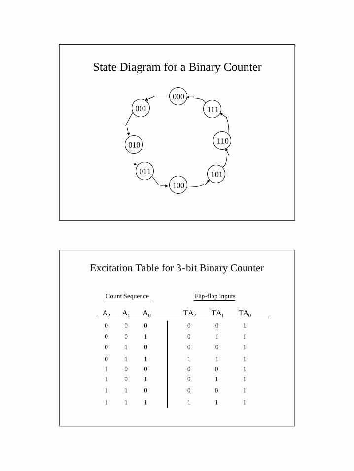
State Diagram for a Binary Counter
000
111
110
101100
001
010
011
Excitation Table for 3-bit Binary Counter
Count Sequence
A2 A1
00
00
10
10
01
01
11
11
A0
0
1
0
1
0
1
0
1
Flip-flop inputs
00
10
00
11
00
10
00
11
1
1
1
1
1
1
1
1
TA0TA2 TA1
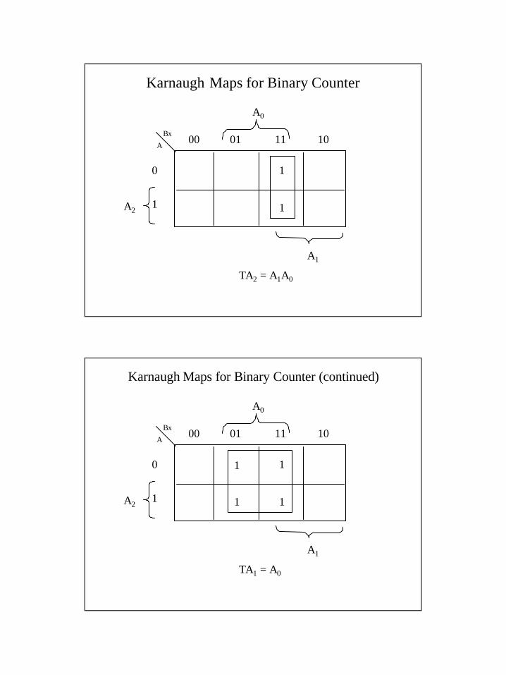
Karnaugh Maps for Binary Counter
Bx
A00 01 11 10
0
1 1
1
TA2 = A1A0
A0
A1
A2
Karnaugh Maps for Binary Counter (continued)
Bx
A00 01 11 10
0
1 1
1
TA1 = A0
A0
A1
A2 1
1
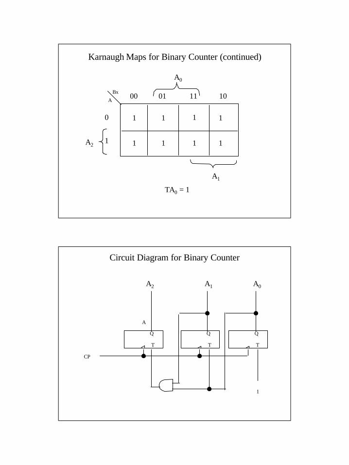
Karnaugh Maps for Binary Counter (continued)
Bx
A00 01 11 10
0
1 1
1
TA0 = 1
A0
A1
A2 1
1
1
1
1
1
Circuit Diagram for Binary Counter
T
Q
T
Q
CP
A
1
T
Q
A2 A0A1