Embed Size (px)
Citation preview
1
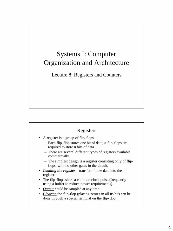
Systems I: Computer Organization and Architecture
Lecture 8: Registers and Counters
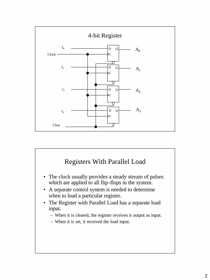
Registers• A register is a group of flip-flops.
– Each flip-flop stores one bit of data; n flip-flops are required to store n bits of data.
– There are several different types of registers available commercially.
– The simplest design is a register consisting only of flip-flops, with no other gates in the circuit.
• Loading the register – transfer of new data into the register.
• The flip-flops share a common clock pulse (frequently using a buffer to reduce power requirements).
• Output could be sampled at any time.• Clearing the flip-flop (placing zeroes in all its bit) can be
done through a special terminal on the flip-flop.
2
4-bit Register
D
C
Q
D
C
Q
D
C
Q
D
C
Q
A0
A1
A2
A3
Clock
Clear
I0
I1
I2
I3
Registers With Parallel Load
• The clock usually provides a steady stream of pulses which are applied to all flip-flops in the system.
• A separate control system is needed to determine when to load a particular register.
• The Register with Parallel Load has a separate load input.– When it is cleared, the register receives it output as input.– When it is set, it received the load input.
3
4-bit Register With Parallel Load
D
C
Q
D
C
Q
D
C
Q
D
C
Q
A0
A1
A2
A3
Clock
I0
I1
I2
I3
Load
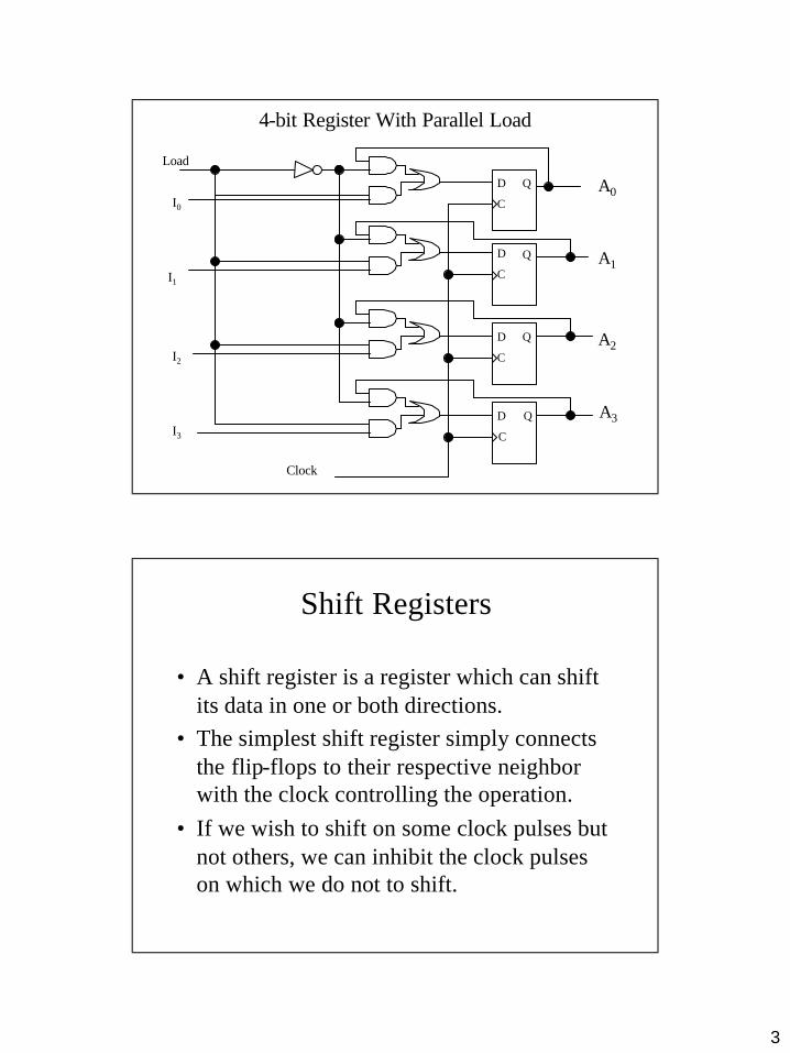
Shift Registers
• A shift register is a register which can shift its data in one or both directions.
• The simplest shift register simply connects the flip-flops to their respective neighbor with the clock controlling the operation.
• If we wish to shift on some clock pulses but not others, we can inhibit the clock pulses on which we do not to shift.
4
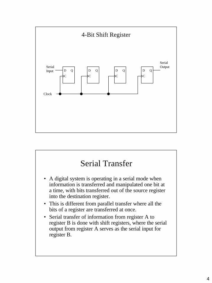
4-Bit Shift Register
D
C
Q D
C
Q D
C
Q D
C
QSerialInput
SerialOutput
Clock
Serial Transfer
• A digital system is operating in a serial mode when information is transferred and manipulated one bit at a time, with bits transferred out of the source register into the destination register.
• This is different from parallel transfer where all the bits of a register are transferred at once.
• Serial transfer of information from register A to register B is done with shift registers, where the serial output from register A serves as the serial input for register B.
5
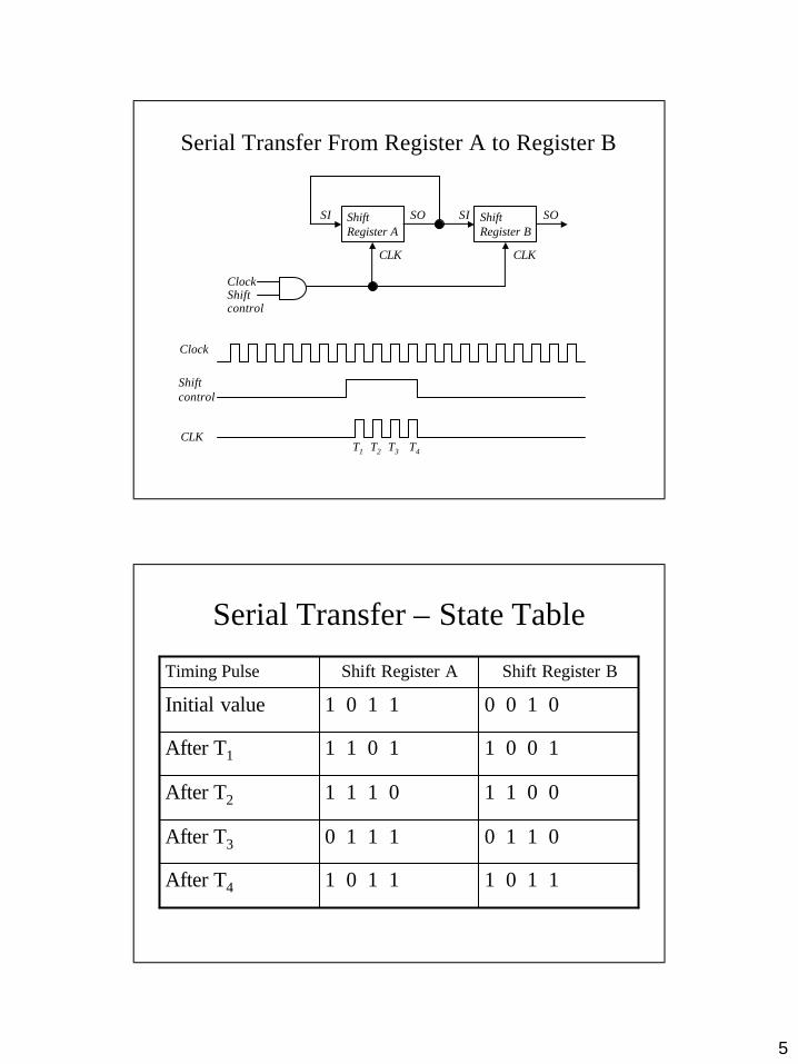
Serial Transfer From Register A to Register B
Shift Register A
Shift Register B
SI SISO SO
CLK CLK
ClockShiftcontrol
Clock
Shiftcontrol
CLKT1 T2 T3 T4
Serial Transfer – State Table
1 0 1 11 0 1 1After T4
0 1 1 00 1 1 1After T3
1 1 0 01 1 1 0After T2
1 0 0 11 1 0 1After T1
0 0 1 01 0 1 1Initial value
Shift Register BShift Register ATiming Pulse
6
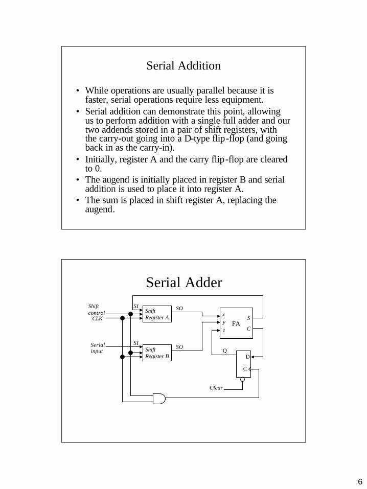
Serial Addition
• While operations are usually parallel because it is faster, serial operations require less equipment.
• Serial addition can demonstrate this point, allowing us to perform addition with a single full adder and our two addends stored in a pair of shift registers, with the carry-out going into a D-type flip-flop (and going back in as the carry-in).
• Initially, register A and the carry flip-flop are cleared to 0.
• The augend is initially placed in register B and serial addition is used to place it into register A.
• The sum is placed in shift register A, replacing the augend.
Serial Adder
Shift Register A
Shift Register B
FAzyx
C
S
D
C
Clear
Q
SO
SO
SI
SISerialinput
CLK
Shiftcontrol
7
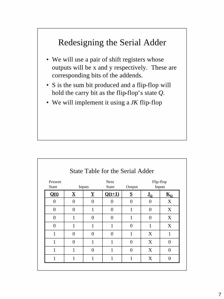
Redesigning the Serial Adder
• We will use a pair of shift registers whose outputs will be x and y respectively. These are corresponding bits of the addends.
• S is the sum bit produced and a flip-flop will hold the carry bit as the flip-flop’s state Q.
• We will implement it using a JK flip-flop
State Table for the Serial Adder
0X11111
0X01011
0X01101
1X10001
X101110
X010010
X010100
X000000KQJQSQ(t+1)YXQ(t)
Present State Inputs
Next State Output
Flip-flop Inputs
8
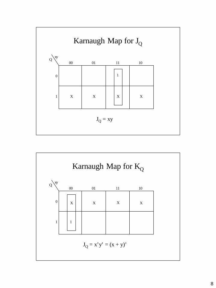
Karnaugh Map for JQ
0100 11 10
1
0
Qxy
1
XXX X
JQ = xy
Karnaugh Map for KQ
0100 11 10
1
0
Qxy
1
XXX X
JQ = x’y’ = (x + y)’
9
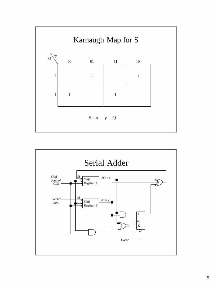
Karnaugh Map for S
0100 11 10
1
0
Qxy
1 1
1 1
S = x ⊕ y ⊕ Q
Serial Adder
Shift Register A
Shift Register B
C
Clear
SO = x
SO = y
SI
SISerialinput
CLK
Shiftcontrol
K
J
10
Bi-directional Shift Registers
• A shift register that can shift in one direction is called a unidirectional shift register.
• A shift register that can shift in either direction is called a bi-directional shift register.
• Some shift register also allow for the simple transfer of data.
General Shift Register• The most general shift register have all of these
capabilities:– An input for clock pulses to synchronize all
operations.– A shift-right operation and serial line input line
associated with the shift-right.– A shift- left operation and serial line input line
associated with the shift- left.– A parallel load operation and n input lines associated
with the parallel transfer.– n parallel output lines.– A control state that leaves the information in the
register unchanged even though the clock pulses are applied.
11
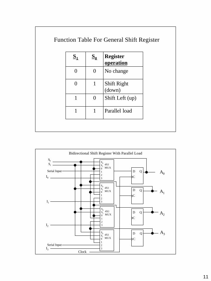
Function Table For General Shift Register
Parallel load11
Shift Left (up)01
Shift Right (down)
10
No change00
Register operation
S0S1
Bidirectional Shift Register With Parallel Load
D
C
Q
D
C
Q
D
C
Q
D
C
Q
A0
A1
A2
A3
Clock
I0
I1
I2
I3
S0S10123
4X1MUX
S0S10123
4X1MUX
S0S10123
4X1MUX
S0S10123
4X1MUX
Serial Input
Serial Input
S0
S1
12
Counters
• A register that goes through a prescribed sequences of states upon the application of an input pulse is called a counter.
• The input pulse may be a clock pulse or may have some other origin.
• A counter that goes through a binary sequence is called a binary counter.
• An n-bit binary counter uses n flip-flops and can count from 0 to 2n-1.
Ripple Counters
• Counters are either ripple counters or synchronous counters.
• In synchronous counters, all flip-flops receive the common clock pulse; therefore they change at the same time.
• In ripple counters, the output of one flip-flop is used as a source for triggering others.
13
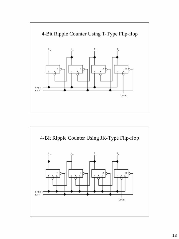
4-Bit Ripple Counter Using T-Type Flip-flop
T CR
A0
Count
T CR
A1
ResetLogic-1
T CR
A2
T CR
A3
4-Bit Ripple Counter Using JK-Type Flip-flop
J CR
A0
Count
J CR
A1
ResetLogic-1
J CR
A2
J CR
A3
KKKK
14
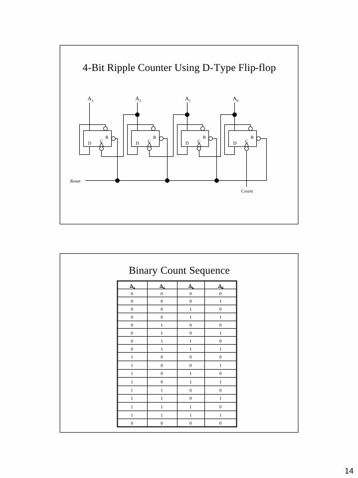
4-Bit Ripple Counter Using D-Type Flip-flop
D CR
A0
Count
Reset
D CR
A1
D CR
A2
D CR
A3
Binary Count Sequence
0000
1111
0111
1011
0011
1101
0101
1001
0001
1110
0110
1010
0010
1100
0100
1000
0000
A0A1A2A3
15
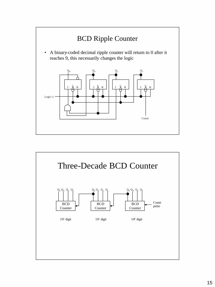
BCD Ripple Counter
• A binary-coded decimal ripple counter will return to 0 after it reaches 9, this necessarily changes the logic
J C K
Q1
Logic-1
Count
J C K
Q2
J C K
Q4
J C K
Q8
Three-Decade BCD Counter
BCDCounter
Q8 Q4 Q2 Q1
BCDCounter
Q8 Q4 Q2 Q1
BCDCounter
Q8 Q4 Q2 Q1
Countpulse
102 digit 101 digit 100 digit
16
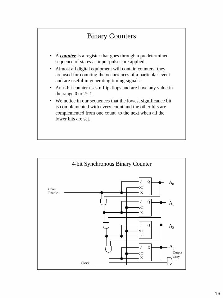
Binary Counters
• A counter is a register that goes through a predetermined sequence of states as input pulses are applied.
• Almost all digital equipment will contain counters; they are used for counting the occurrences of a particular event and are useful in generating timing signals.
• An n-bit counter uses n flip-flops and are have any value in the range 0 to 2n-1.
• We notice in our sequences that the lowest significance bit is complemented with every count and the other bits are complemented from one count to the next when all the lower bits are set.
4-bit Synchronous Binary Counter
J
C
Q
J
C
Q
J
C
Q
J
C
Q
A0
A1
A2
A3
Clock
K
K
K
K
CountEnable
Outputcarry
17
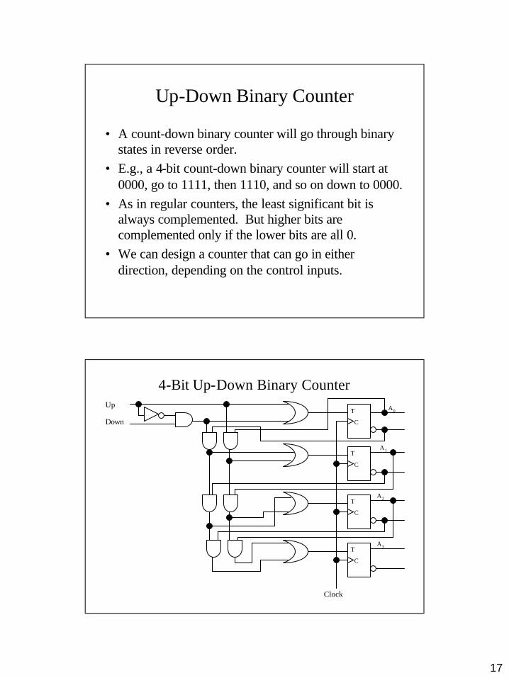
Up-Down Binary Counter
• A count-down binary counter will go through binary states in reverse order.
• E.g., a 4-bit count-down binary counter will start at 0000, go to 1111, then 1110, and so on down to 0000.
• As in regular counters, the least significant bit is always complemented. But higher bits are complemented only if the lower bits are all 0.
• We can design a counter that can go in either direction, depending on the control inputs.
4-Bit Up-Down Binary Counter
T
C
T
C
T
C
T
C
Clock
Up
Down
A0
A1
A2
A3
18
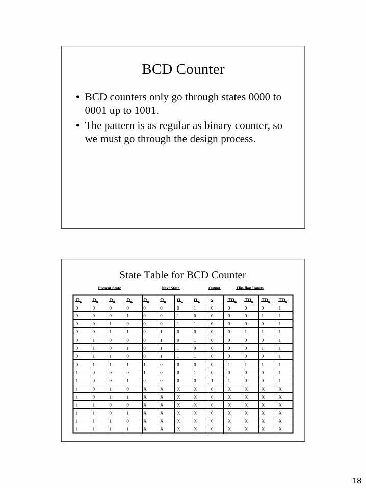
BCD Counter
• BCD counters only go through states 0000 to 0001 up to 1001.
• The pattern is as regular as binary counter, so we must go through the design process.
State Table for BCD Counter
XXXX0XXXX1111
XXXX0XXXX0111
XXXX0XXXX1011
XXXX0XXXX0011
XXXX0XXXX1101
XXXX0XXXX0101
1001100001001
1000010010001
1111000011110
1000011100110
1100001101010
1000010100010
1110000101100
1000011000100
1100001001000
1000010000000
TQ 1TQ 2TQ 4TQ 8yQ 1Q 2Q 4Q 8Q 1Q 2Q 4Q 8
Present State Next State Output Flip-flop Inputs
19
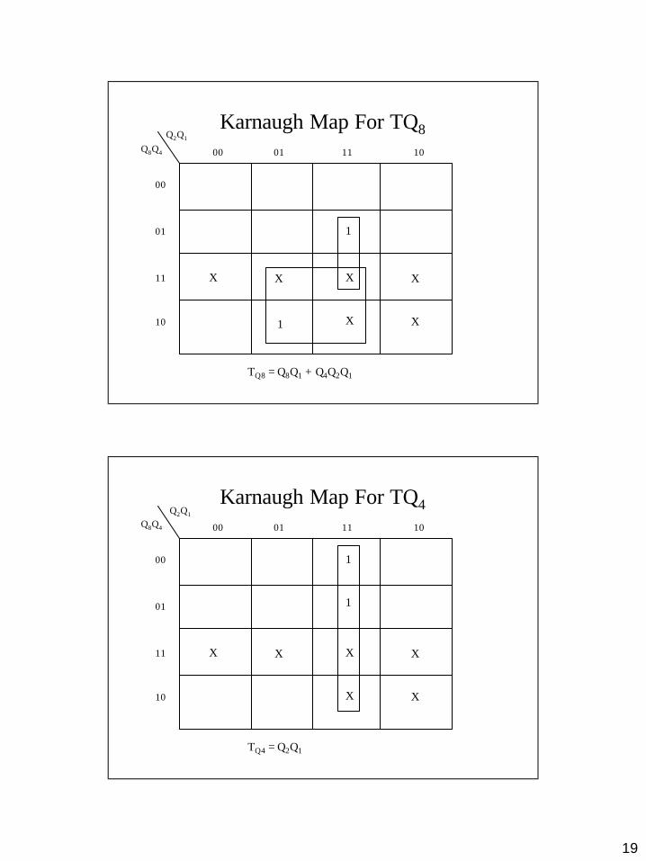
Karnaugh Map For TQ801 11 1000
01
11
10
00
XX
XXXX
1
1
TQ8 = Q8Q1 + Q4Q2Q1
Q8Q4
Q2Q1
Karnaugh Map For TQ401 11 1000
01
11
10
00
XX
XXXX
1
1
TQ4 = Q2Q1
Q8Q4
Q2Q1
20
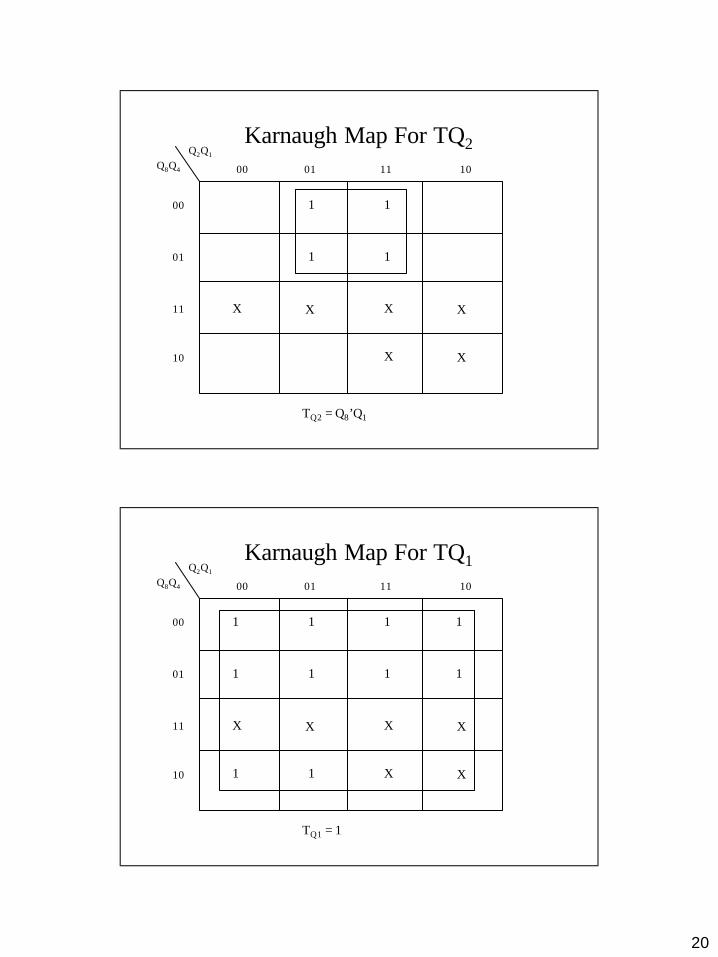
Karnaugh Map For TQ201 11 1000
01
11
10
00
XX
XXXX
1
TQ2 = Q8’Q1
1 1
1
Q8Q4
Q2Q1
Karnaugh Map For TQ101 11 1000
01
11
10
00
XX
XXXX
1
TQ1 = 1
1 1
1
Q8Q4
Q2Q1
11
1
1
1
1
21
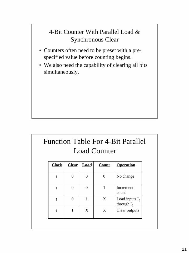
4-Bit Counter With Parallel Load & Synchronous Clear
• Counters often need to be preset with a pre-specified value before counting begins.
• We also need the capability of clearing all bits simultaneously.
Function Table For 4-Bit Parallel Load Counter
Clear outputsXX1↑
Load inputs I0through I3
X10↑
Increment count
100↑
No change000↑
OperationCountLoadClearClock
22
J
C
Q
J
C
Q
J
C
Q
J
C
Q
A0
A1
A2
A3
Clock
K
K
K
K
Load
CountI0
I1
I2
I3
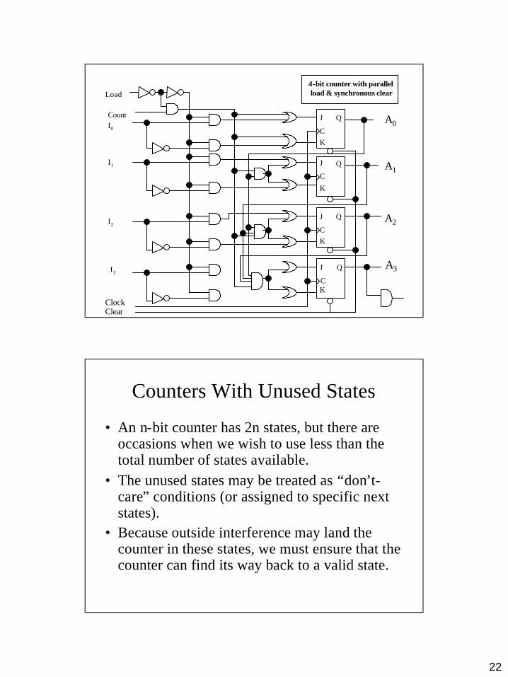
4-bit counter with parallelload & synchronous clear
Clear
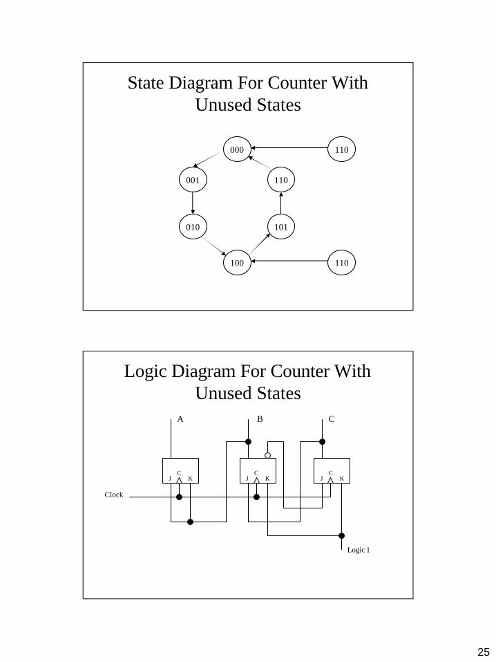
Counters With Unused States
• An n-bit counter has 2n states, but there are occasions when we wish to use less than the total number of states available.
• The unused states may be treated as “don’t-care” conditions (or assigned to specific next states).
• Because outside interference may land the counter in these states, we must ensure that the counter can find its way back to a valid state.
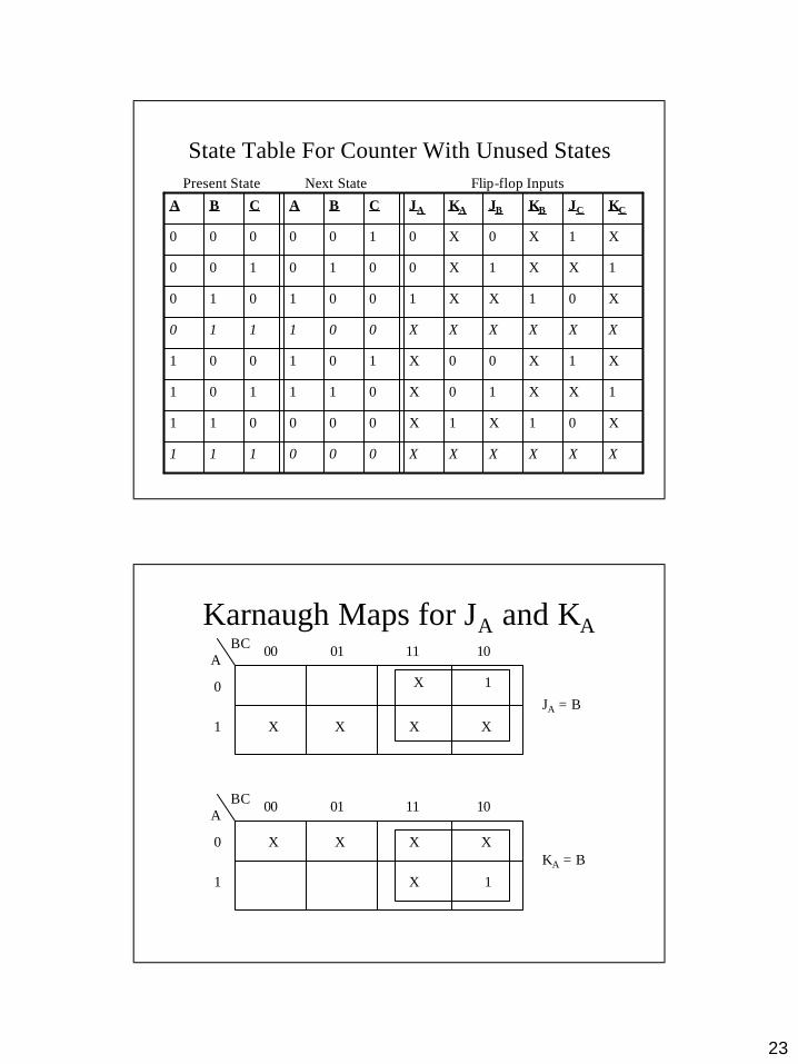
23
State Table For Counter With Unused States
X01X1X000011
XXXXXX000111
1XX10X011101
X1X00X101001
XXXXXX001110
X01XX1001010
1XX1X0010100
X1X0X0100000
KCJCKBJBKAJACBACBA
Next StatePresent State Flip-flop Inputs
Karnaugh Maps for JA and KABC
A0100 11 10
0
1 XX X
X 1
X
BCA
0100 11 10
0
1
XX X
X 1
XKA = B
JA = B
24
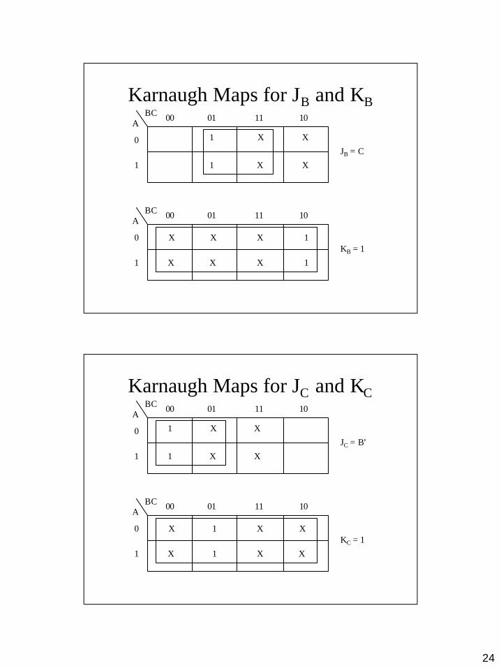
Karnaugh Maps for JB and KBBC
A0100 11 10
0
1
X X
X
1
1 X
BCA
0100 11 10
0
1
XX
X X 1X
KB = 1
JB = C
X 1
Karnaugh Maps for JC and KCBC
A0100 11 10
0
1
X X
X
1
1 X
BCA
0100 11 10
0
1
XX
XX1X
KC = 1
JC = B’
X1
25
State Diagram For Counter With Unused States
000
001
010
100
110
101
110
110
Logic Diagram For Counter With Unused States
CJ K
CJ K
CJ K
B CA
Clock
Logic 1
26
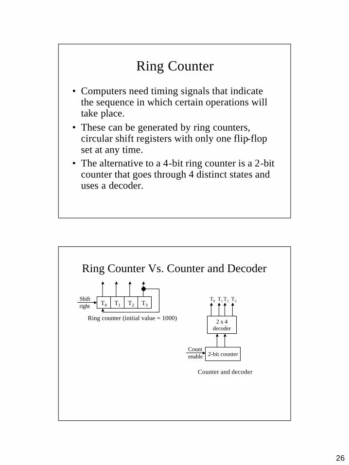
Ring Counter
• Computers need timing signals that indicate the sequence in which certain operations will take place.
• These can be generated by ring counters, circular shift registers with only one flip-flop set at any time.
• The alternative to a 4-bit ring counter is a 2-bit counter that goes through 4 distinct states and uses a decoder.
Ring Counter Vs. Counter and Decoder
T0 T1 T2 T3Shiftright
Ring counter (initial value = 1000) 2 x 4decoder
T1 T2 T3T0
2-bit counterCountenable
Counter and decoder
27
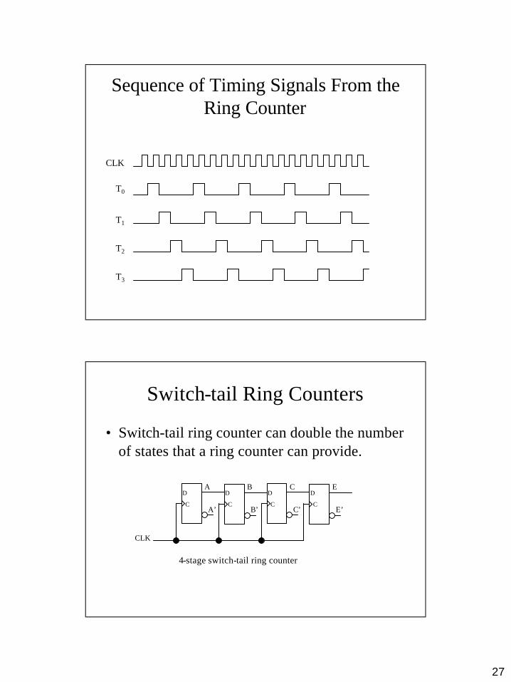
Sequence of Timing Signals From the Ring Counter
T0
T1
T2
T3
CLK
Switch-tail Ring Counters
• Switch-tail ring counter can double the number of states that a ring counter can provide.
C
DA
A’C
DB
B’C
DC
C’C
DE
E’
4-stage switch-tail ring counter
CLK
28
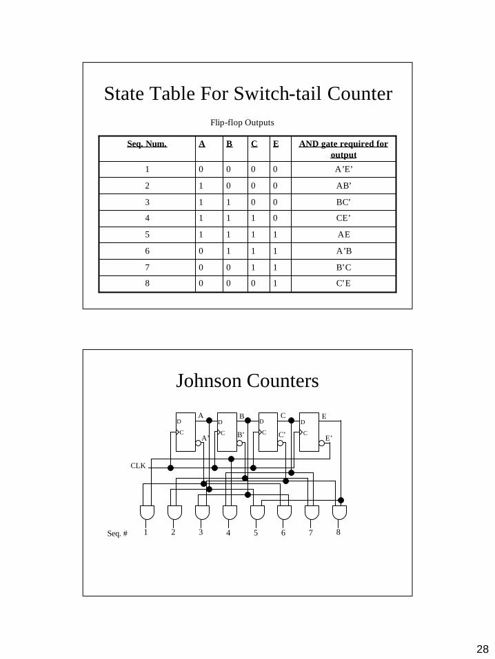
State Table For Switch-tail Counter
C’E10008
B’C11007
A’B11106
AE11115
CE’01114
BC’00113
AB’00012
A’E’00001
AND gate required for output
ECBASeq. Num.
Flip-flop Outputs
Johnson Counters
C
DA
A’C
DB
B’ C
DC
C’ C
DE
E’
CLK
Seq. # 21 3 4 5 6 7 8