Embed Size (px)
Citation preview
Tantalum nitride nanotube photoanodes: establishing a
beneficial back-contact by lift-off and transfer to titanium
nitride layer
Lei Wang, a Anca Mazare,
a Imgon Hwang,
a and Patrik Schmuki
a,b,*
a Department of Materials Science and Engineering, WW4-LKO, University of Erlangen-
Nuremburg, Martensstrasse 7, D-91058 Erlangen, Germany.
b Department of Chemistry, King Abdulaziz University, Jeddah, Saudi Arabia
* E-mail: [email protected]
Abstract
In this work we introduce the use of TiN/Ti2 N layers as a back contact for lifted-off
membranes of anodic Ta3N5 nanotube layers. In photoelectrochemical H2 generation
experiments under simulated AM 1.5G light, shift of the onset potential for anodic
photocurrents to lower potentials is observed, as well as a higher magnitude of the
photocurrents compared to conventional Ta3N5 nanotubes (~0.5 V RHE ). We ascribe
this beneficial effect to the improved conductive properties of the TiNx -based back
contact layer that enables a facilitated electron-transport for tantalum-nitride based
materials to the conductive substrate.
Key words: tantalum nitride; nanotube membranes; titanium nitride; water splitting
Link to the published article: http://dx.doi.org/10.1016/j.elecom.2016.08.012
1
1. Introduction
Ta3N5 is considered to be one of the most important semiconductor materials for
photoelectrochemical (PEC) water splitting. It has a visible-light active band gap of
~2.1 eV that embraces the H2O H2/O2 reduction-oxidation potentials, and thus may
yield a 15.9% theoretical maximum solar-to-hydrogen (STH) conversion efficiency
[1-9]. Extensive research has focused on nanostructuring the Ta3N5 photoelectrodes,
in the form of nanoparticles, nanorods, or nanotubes [10-15]. 1-dimensional (1D)
nanorod/nanotube structures provide the advantage, not only of a high surface area,
but also of a directional and controllable light and electron management compared to
the nanoparticles. For the synthesis of Ta3N5 nanostructures, first usually Ta2O5
structures are synthesized, that are then converted to Ta3N5 by a thermal annealing
treatment in NH3. However, thick nanoparticle-based Ta3N5 photoelectrodes (e.g.
deposited on conductive layers (FTO) by electrophoretic deposition) suffer from an
inefficient electron transfer across the interface between the Ta3N5 and the
conductive substrate [10,14]. To overcome this issue, a refined necking treatment (i.e.
additional TaCl5 decoration and annealing) was introduced and improves the charge
transfer not only between particles but also at the particle/substrate interface [10,11].
Recently, excellent mechanical and electric contacts were reported by using a
transferred particle layer on a Ti/Ta-metal contact [12,13]. More recently a film
transfer method based on Ta2O5 films on silicon for the Ta3N5 photoelectrodes was
reported to achieve control in film thickness and to establish a defined back contact
[14]. These data demonstrate that various metallic (Nb, Ti, Ta) and semiconductor
2
(NbNx , CdS) layers can be used as back contacts to improve the PEC performance of
Ta3N5 photoelectrodes.
For Ta3N5 photoelectrodes grown on or from Ta foils, either 1D nanostructures
such as nanorods and nanotubes or compact films, even a higher PEC water splitting
performance was reported compared with nanoparticle-based photoelectrodes. Also
for these structures back contacts are a crucial factor for the quality of
electrode-substrate connection [7,15-20]. Previous work has shown that the formation
of Ta-subnitride layers (Ta2N, TaN) underneath anodic Ta3N5 nanotubes can enhance
their efficiency due to a higher conductivity than Ta3N5, and therefore improve the
charge transfer to the back contact [7,15]. However, to build photoanodes based on
nanotubular Ta3N5 and explore different back contact layers, formation of
free-standing membranes is needed. Similarly to the procedure for obtaining TiO2
nanotube membranes, under optimized conditions Ta2O5 nanotube membranes can be
obtained, that can then be converted to Ta3N5 . The methods used for obtaining
membranes include either voltage pulses or an annealing-anodization-etching
sequence [21] to separate the layer from the Ta metal substrate. In the present work,
we use the latter, i.e. after nanotube growth, the layers are crystallized (air annealing),
anodized again to grow an amorphous nanotubular oxide layer underneath, which then
can be selectively dissolved in a HF aqueous solution. This procedure leads to Ta3N5
nanotube membranes and thus enables the possibility of transferring them to desired
conductive layers as back contacts for 1D Ta3N5 nanotubular structures. Ideal ohmic
back contacts should be highly conductive and have a work function corresponding to
3
the Fermi level of the semiconductor at flatband situation.
For this we use in the current work TiN/Ti2N layers as a back contact. They seem
ideal as they show a virtually metallic behavior and provide an excellent match of the
work functions (W F (TiN x ) ≈ 3.5-4.4 eV) [22]. Here we show that indeed, by using
this back contact, the anodic photoresponse under simulated AM 1.5G light shifts to
significantly lower onset potentials. We ascribe this to the improved charge transfer
properties of the back contact layer that enables a facilitated electron-transport to the
substrate.
2. Experimental
The Ta2O5 NTs were prepared by anodizing Ta foil (99.9%, 0.1 mm, Advent) in a
two electrode electrochemical cell with a Pt counter electrode. The anodization
experiments were performed at 60 V (with a maximum current density set at 0.1 mA
cm -2 ) in a sulfuric acid (H2SO4 , 98%) electrolyte containing 0.8 wt.% NH 4 F and
13.6 vol% DI water. The anodization times were 5, 10, and 15 min, respectively. Then,
samples were immersed in ethanol for 5 min and dried in N2 . For producing Ta2O5
nanotube membranes, the as-prepared Ta2O5 nanotube layers were annealed in air at
450 °C for 1 h, followed by anodizing at 80 V in the same fresh electrolyte. The layers
were then detached from the Ta substrate by immersion in an aqueous 5% HF solution
for 30 min at room temperature. For the preparation of membrane photoelectrodes, the
Ta2O5 NT membranes were coated with a Ti nanoxide paste (Solaronix SA) on Ti
foils by doctor blading, followed by annealing in a NH3 atmosphere at 950 °C to
4
convert to Ta3N5/TiNx (TiNx from Ti nanoxide). The temperature was ramped up
with a heating rate of 10 °C min-1 , kept at the desired temperature for 1 h, and finally
the furnace was cooled down to room temperature.
The photoelectrochemical experiments were carried out under simulated AM 1.5G
(100mW cm-2 ) illumination provided by a solar simulator (300 W Xe with optical
filter, Solarlight; RT). 1 M KOH aqueous solution was used as an electrolyte. The
Ta3N5 layers were prior to measurements coated with a Co(OH) x co-catalyst as
described in [15]. Photocurrent vs.voltage (I-V) characteristics were recorded by
scanning the potential from 1.0 V to 0.6 V (vs. Ag/AgCl (3 M KCl)) with a scan rate
of 10 mV s -1 using a Jaissle IMP 88 PC potentiostat. Electrochemical impedance
spectroscopy (EIS) measurements were performed using a Zahner IM6 (Zahner
Elektrik, Kronach, Germany). EIS measurements were performed by applying 1.23 V
RHE at a frequency range of 105 Hz to 0.01 Hz with an amplitude of 10 mV in the
dark. Solid-state conductivity measurements were carried out in an adapted scanning
electron microscope (SEM, TESCAN LYRA3 XMU) by 2-point measurements using
a semiconductor characterization system (Keithley 4200-SCS). Tungsten tips were
used as electrical contacts between tube tops and substrate. Resistivity values were
then obtained from I-V curves with 5 mV/s sweep rate.
A field-emission scanning electrode microscope (Hitachi FE-SEM S4800, Japan)
was used for the morphological characterization of the electrodes. X-ray diffraction
(X’pert Philips MPD with a Panalytical X’celerator detector, Germany) was carried
out using graphite monochromized Cu Kα radiation (Wavelength 0.154056 nm).
5
Chemical characterization was carried out by X-ray photoelectron spectroscopy (PHI
5600, spectrometer, USA) using AlKα monochromatized radiation, peaks were
calibrated to C1s 284.8 eV.
3. Results and discussion
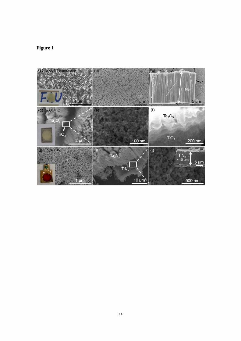
Ta2O5 nanotube (NT) membranes were grown by electrochemical anodization of
Ta, and further proceeded to membranes as described in the experimental part. The
resulting both-end open NT-layers consist of aligned nanotubes, with an individual
diameter of ~50 nm and a length of 10-12 μm (Fig. 1a-c). The thickness of such
Ta2O5 NT membranes can be adjusted between 10 to 20 μm, by increasing the
anodization time from 5 to 15 min (~15 μm and ~20 μm for 10 min and 15 min,
respectively). Nevertheless, membranes with a thickness lower than 7 μm cannot be
separated from the Ta substrate without breakage. The oxide membranes were then
connected by doctor blading to a TiO2 nanoparticle layer (~10 μm) on a Ti foil
(Ta2O5 /TiO2 , Fig. 1d-f); in such electrodes, ~10 nm diameter TiO2 nanoparticles
can be observed underneath the NT membrane layer (Fig. 1d,e) and in between the
nanotubes (Fig. 1f). The Ta2O5/TiO2 structure is then subjected to nitridation at
950 °C (optimized conditions) and a Ta3N5/TiN x electrode is obtained (Fig. 1g-i).
The nanotube diameter decreases to ~40 nm as well as the thickness, to ~8 μm, due to
the volume decrease when converting Ta2O5 to Ta3N5. Additionally, well-connected
nano-sized porous TiNx particles are observed underneath the NT membrane (Fig.
1h,i). The thickness of the TiNx layer is about 10 μm (inset Fig. 1i). The TiN x
6
nanoparticles and Ti foil act as a back contact and a conductive substrate for the
Ta3N5 membrane, respectively.
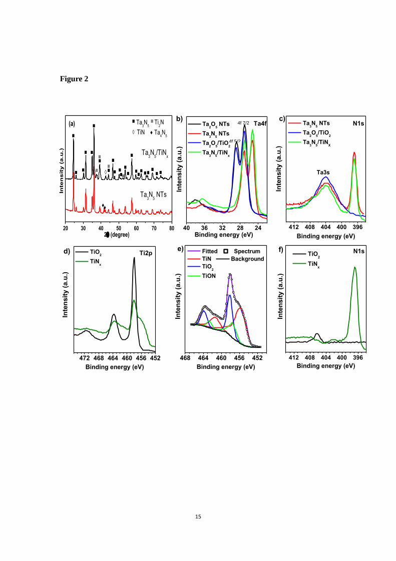
To determine the phase and chemical composition of the as-formed and nitrided
nanotubes or membranes, XRD and XPS investigations were performed. Fig. 2a
shows the XRD patterns of Ta3N5 NT on Ta foil (Ta3N5 NT) and the membrane with
TiNx back contact layer (Ta3N5/TiNx ). Both patterns show monoclinic Ta3N5
phases, while for the Ta3N5/TiNx electrode peaks corresponding to TiN and Ti2N are
also observed. For Ta3N5 NT, in addition, a Ta 4 N peak at 41° and 42° can be
identified, that is generally attributed to over-nitridation [7]. XPS measurements of
the Ta2O5/Ta3N5 nanotubes or membranes are listed in Fig. 2b-f. The Ta 4f 7/2 peak
is shifted from 27 eV for Ta2O5 to 25 eV for Ta3N5 (Fig. 2b), and for both nitrided
nanotubes on Ta or Ti foil, clear N 1s peaks at 397 eV are observed (Fig. 2c). In
addition, for the TiN x back contact layer, the Ti 2p and N 1s peaks (Fig 2d, f) after
nitridation clearly indicate the presence of the TiN phase – see the Ti 2p peak fitting in
Fig. 2e. Please note that at the top surface due to the contact with air, TiO2 and very
small amounts of TiON phase are also detected.
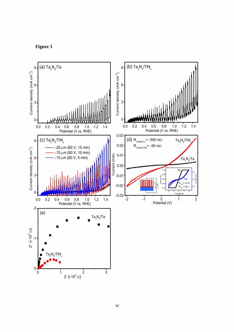
Fig. 3a,b shows the transient photocurrent-potential curves of Ta3N5 NT
membrane on Ti foil (Ta3N5/TiNx ) and for comparison purposes, Ta3N5 NTs on a Ta
foil. The photocurrent of the TiN x supported electrode increases significantly at 0.6 V
RHE and reaches 5.3 mA cm -2 at 1.2 V RHE (Fig. 3b) which is consistent with
literature reported values for 1D nanostructures. More importantly, an anodic
photoresponse is observed at potentials below 0.2 V RHE (whereas in literature this
7
occurs at ~0.5 [7,15,17,18]), which indicates a preferable band alignment in the
electrode to reduce the onset for PEC oxygen evolution from water. Additionally, we
investigated the influence of the nanotube membrane thickness on the photoresponse
of Ta3N5 electrodes as shown in Fig. 3c. The higher thicknesses of NT membranes,
i.e. ~15 μm and ~20 μm, lead to a lower photocurrent due to an increased
recombination of charge carriers. However, the ~15 μm NT membrane (anodization at
60 V for 10 min) still shows a low onset potential of 0 V RHE.
The electrical properties of nanotubes and membrane were evaluated by two-point
conductivity measurements and show a 5 times decrease in the resistance of the layers
and an increased electric conductivity of the membrane on the TiNx back contact
layer (Fig. 3d). Please note that TiNx shows virtual metallic conductivity compared to
the TaNx phase (inset of Fig. 3d). Moreover, electrochemical impedance spectroscopy
measurements confirm a lower charge transfer resistance of the membrane on TiNx
(Rct 10170 Ω) compared to the nanotube (Rct 50230 Ω), see Fig. 3e. These findings
are in line with the work function of TiNx that varies from 3.5 and 4.4 eV [22], and
thus corresponds well to the flat band potential of the Ta3N5 which is at 0.2 V RHE .
Therefore, it can be concluded that TiNx forms an energetically suitable ohmic
contact with Ta3N5 at the interface. The above results thus show that the existence of
TiNx layer as back contact provides a beneficial effect on the charge transfer
resistance, thus provides more efficient photoelectron-hole separation, and thus
improves the PEC performance of Ta3N5 photoelectrodes [23].
8
4. Summary
In the current work we successfully form a photoanode, consisting of a Ta3N5
nanotube membrane fixed on a Ti foil by means of a TiNx interface layer. The
fabrication consists of a sequence of anodization, doctor-blading, and nitridation. On
the TiNx back contact, Ta3N5 NT membrane photoanodes with Co(OH)x
decoration show an anodic photocurrent of 5.3 mA cm-2 at 1.2 V RHE in 1 M KOH
under simulated AM 1.5G illumination, and a significantly increased response at low
anodic potentials. The shift in the onset of the anodic photoresponse to a potential of
0.2 V RHE is ascribed to the high conductivity and a favorable Fermi level of the
TiNx – back contact (compared to other back contacts). It should be noted that many
parameters of the subnitrides can further be optimized to explore the full potential of
the current synthesis. However, the present results clearly indicate that a TiNx as
underlayer significantly enhances the photoelectrochemical water splitting of tantalum
nitride photoanodes.
Acknowledgments
The authors would like to acknowledge DFG SPP1615 and ERC for the financial
support.
References
1. D. Yokoyama, H. Hashiguchi, K. Maeda, T. Minegishi, T. Takata, R. Abe, J. Kubota,
K. Domen, Ta3N5 photoanodes for water splitting prepared by sputtering, Thin Solids
9
Films 519 (2011) 2087‒2092.
2. S. S. K. Ma, T. Hisatomi, K. Maeda, Y. Moriya, K. Domen, Enhanced water
oxidation
on Ta3N5 photocatalysts by modification with alkaline metal salts, J. Am. Chem. Soc.
134 (2012) 19993‒19996.
3. P. Zhang, J. Zhang, J. Gong, Tantalum-based semiconductors for solar water
splitting,
Chem. Soc. Rev. 43 (2014) 4395‒4422.
4. J. Hou, Z. Wang, C. Yang, H. Cheng, S. Jiao, H. Zhu, Cobalt-bilayer catalyst
decorated Ta3N5 nanorod arrays as integrated electrodes for photoelectrochemical
water oxidation, Energy Environ. Sci. 2013, 6, 3322‒3330.
5. Y. Cong, H. S. Park, S. Wang, H. X. Dang, F.–R. R Fan, C. B. Mullins, A. J. Bard,
Synthesis of Ta3N5 nanotube arrays modified with electrocatalysts for
photoelectrochemical water oxidation, J. Phys. Chem. C 116 (2012) 14541‒14550.
6. G. Hitoki, A. Ishikawa, T. Takata, J. N. Kondo, M. Hara, K. Domen, Ta3N5 as a
novel visible light-driven photocatalyst (λ < 600 nm), Chem. Lett. 7 (2002) 736‒737.
7. (a) Y. Li, T. Takata, D. Cha, K. Takanabe, T. Minegishi, J. Kubota, K. Domen,
Vertically aligned Ta3N5 nanorod arrays for solar-driven photoelectrochemical water
splitting, Adv. Mater. 25 (2013) 125‒131; (b) Y. Li, L. Zhang, A. Torres-Pardo, J. M.
González-Calbet, Y. Ma, P. Oleynikov, O. Terasaki, S. Asahina, M. Shima, D. Cha, L.
Zhao, K. Takanabe, J. Kubota, K. Domen, Cobalt phosphate-modified barium-doped
tantalum nitride nanorod photoanode with 1.5% solar energy conversion efficiency,
10
Nat.
Commun. 4 (2013) 2566.
8. S. Chen, S. Shen, G. Liu, Y. Qi, F. Zhang, C. Li, Interface engineering of a CoOx
/Ta3N5 photocatalyst for unprecedented water oxidation performance under
visible-light-Irradiation, Angew. Chem. Int. Ed. 54 (2015) 3047‒3051.
9 G. Fu, S. Yan, T. Yu, Z. Zou, Oxygen related recombination defects in Ta3N5
water splitting photoanode, Appl. Phys. Lett. 107 (2015) 171902‒171905.
10. M. Higashi, K. Domen, R. Abe, Fabrication of efficient TaON and Ta3N5
photoanodes for water splitting under visible light irradiation, Energy Environ. Sci. 4
(2011) 4138‒4147.
11. Z. Wang, Y. Qi, C. Ding, D. Fan, G. Liu, Y. Zhao, C. Li, Insight into the charge
transfer in particulate Ta3N5 photoanode with high photoelectrochemical
performance, Chem. Sci. 7 (2016) 4391‒4399.
12. J. Seo, T. Takata, M. Nakabayashi, T. Hisatomi, N. Shibata, T. Minegishi, K.
Domen,
Mg-Zr cosubstituted Ta3N5 photoanode for lower-onset-potential solar-driven
photoelectrochemical water splitting, J. Am. Chem. Soc. 137 (2015) 12780‒12783.
13. K. Ueda, T. Minegishi, J. Clune, M. Nakabayashi, T. Hisatomi, H. Nishiyama, M.
Katayama, N. Shibata, J. Kubota, T. Yamada, K. Domen, Photoelectrochemical
oxidation of water using BaTaO2 N photoanodes prepared by particle transfer method,
J. Am. Chem. Soc. 137 (2015) 2227‒2230.
14. C. Wang, T. Hisatomi, T. Minegishi, M. Nakabayashi, N. Shibata, M. Katayama,
11
K. Domen, Thin film transfer for the fabrication of tantalum nitride photoelectrodes
with controllable layered structures for water splitting, Chem. Sci. 2016, DOI:
10.1039/C6SC01763K.
15. (a) L. Wang, F. Dionigi, N. T. Nguyen, R. Kirchgeory, M. Gliech, S. Grigoresca,
P. Strasser, P. Schmuki, Tantalum nitride nanorod arrays: Introducing Ni-Fe layered
double hydroxides as a cocatalyst strongly stabilizing photoanodes in water splitting,
Chem. Mater. 27 (2015) 2360‒2366; (b) L. Wang, N. T. Nguyen, X. Zhou, I. Hwang,
M. S. Killian, P. Schmuki, Enhanced Charge Transport in Tantalum Nitride Nanotube
Photoanodes for Solar Water Splitting, ChemSusChem 8 (2015) 2615‒2620; (c) L.
Wang, X. Zhou, N. T. Nguyen, I. Hwang, P. Schmuki, Strongly Enhanced Water
Splitting Performance of Ta3N5 Nanotube Photoanodes with Subnitrides, Adv. Mater.
28 (2016) 2432‒2438.
16. Z. Su, L. Wang, S. Grigorescu, K. Lee, P. Schmuki, Hydrothermal growth of
highly
oriented single crystalline Ta 2 O 5 nanorod arrays and their conversion to Ta3N5 for
efficient solar driven water splitting, Chem. Commun. 50 (2014) 15561‒15564.
17. P. Zhang, T. Wang, J. Zhang, X. Chang, J. Gong, Bridging the transport pathway
of
charge carriers in a Ta3N5 nanotube array photoanode for solar water splitting,
Nanoscale 7 (2015) 13153‒13158.
18. M. Li, W. Luo, D. Cao. X. Zhao, Z. Li, T. Yu, Z. Zou, A co-catalyst-loaded Ta3N5
photoanode with a high solar photocurrent for water splitting upon facile removal of
12
the surface layer, Angew. Chem. Int. Ed. 52 (2013) 11016‒11020.
19. G. Liu, J. Shi, F. Zhang, Z. Chen, J. Han, C. Ding, S. Chen. Z. Wang, H. Han, C.
Li, A tantalum nitride photoanode modified with a hole-storage layer for highly stable
solar
water splitting, Angew. Chem. Int. Ed. 53 (2014) 7295‒7299.
20. C. Zhen, L. Wang, G. Liu, G. Q. Lu, H.-M. Cheng, Template-free synthesis of
Ta3N5 nanorod arrays for efficient photoelectrochemical water splitting, Chem.
Commun. 49 (2013) 3019‒3021.
21. F. Mohammadpour, M. Moradi, K. Lee, G. Cha, S. So, A. Kahnt, D. M. Guldi, M.
Altomare, P. Schmuki, Enhanced performance of dye-sensitized solar cells based on
TiO2 nanotube membranes using an optimized annealing profile, Chem. Commun. 51
(2015) 1631‒1634.
22. B. P. Luther, S. E. Mohney, T. N. Jackson, Titanium and titanium nitride contacts
to n-type gallium nitride, Semicond. Sci. Technol. 13 (1998) 1322‒1327.
23. R. Khanna, S. Yamaguchi, A. Valanezhad, T. Kokubo. T. Matsushita, Y. Naruta, H.
Takadama, N-doped titanate nanostructures on gradient surface layer of one
dimensional nanofibers synthesized on Ti electrode by chemical and thermal
treatments, J. Mater. Chem. A 2 (2014) 1809‒1817.
13
Figure 1. SEM top, cross sectional, and bottom images of (a-c) Ta2O5 NT membrane,
(d-f) Ta2O5 NT membrane on Ti foil, and (g-i) Ta3N5 NT membrane on Ti foil. The
electrode was anodized at 60 V for 5 min. Insets of a, d, and g show optical images of
membranes. Inset of (i) shows the cross sectional image of TiNx subnitride layer.
Figure 2. (a) XRD patterns of Ta3N5 NTs on Ta foil and Ta3N NT membrane on Ti
foil (Ta3N5 /TiN x ); (b-f) high resolution XPS spectra of (b) Ta4f for Ta2O5 and
Ta3N5 NTs, Ta2O5/TiO2 and Ta3N5/TiN x , (c) N1s for Ta2O5 and Ta3N5 NTs,
Ta3N5/TiN x , (d-f) Ti2p and N1s for TiO2, TiN x with (e) peak fitting of Ti2p for
TiN x .
Figure 3. (a,b) PEC water splitting properties of (a) Co(OH) x treated Ta3N5 NTs and
(b) the corresponding membranes on Ti (Ta3N5 /TiN x ) (nanotubes were obtained at
60 V, 5 min); (c) PEC water splitting properties of Co(OH) x decorated Ta3N5/TiN x ,
as a function of the starting length of the Ta2O5 membranes converted to Ta3N5 . The
electrolyte is 1 M KOH under simulated AM 1.5G light (100 mW cm-2 ); (d)
electrical resistance and (e) electrochemical impedance spectroscopy (EIS) of Ta3N5
NTs and Ta3N5/TiNx . Inset of (d) shows the corresponding results of TiNx and
TaNx.
14
Figure 1
15
Figure 2
40 36 32 28 24 412 408 404 400 396
472 468 464 460 456 452 468 464 460 456 452
b)Ta4f
Inte
nsit
y (
a.u
.)
Binding energy (eV)
Ta2O
5 NTs
Ta3N
5 NTs
Ta2O
5/TiO
2
Ta3N
5/TiN
x
c)N1s
Inte
nsit
y (
a.u
.)
Binding energy (eV)
Ta3N
5 NTs
Ta2O
5/TiO
2
Ta3N
5/TiN
X
Ta3s
d) Ti2p
Inte
nsit
y (
a.u
.)
Binding energy (eV)
TiO2
TiNx
e)
Inte
nsit
y (
a.u
.)
Binding energy (eV)
Fitted Spectrum
TiNa Background
TiO2
TiON
412 408 404 400 396
TiO2
TiNx
N1sf)
Inte
nsit
y (
a.u
.)
Binding energy (eV)
4f 7/2
4f 5/2
20 30 40 50 60 70 80
Ta3N
5 NTs
2 (degree)
Inte
ns
ity
(a
.u.)
Ta3N
5/TiN
x
Ti2NTa
3N
5
TiN Ta4N
5
(a)
16
Figure 3
0
3
6
9
20 m (60 V, 15 min)
15 m (60 V, 10 min)
10m (60 V, 5 min)
Cu
rre
nt
de
nsity (
mA
cm
-2)
0.0 0.2 0.4 0.6 0.8 1.0 1.2 1.4 Potential (V vs. RHE)
(c) Ta3N
5/TiN
x
0 1 2 30
-1
-2
Ta3N
5/TiN
x
Z(1
04
)
Z (104 )
Ta3N
5/Ta
(e)
-2 -1 0 1 2
-2 -1 0 1 2
TaNx
-0.5
0.0
0.5
-0.10
0.00
-0.05
0.05
Curr
ent (m
A)
Potential (V)
Curr
ent (A
)
0.10 TiNx
RTaNx
=3m
RTiNx
=20
R
Ta3N
5/TiN
x
-0.03
-0.02
-0.01
0.00
0.01
0.02
Cu
rre
nt
(mA
)
Potential (V)
0.03
Ta3N
5/Ta
(d) RTa3N5/Ta
= 500 m
RTa3N5/TiNx
= 95 m
0
3
6
9
0.0 0.2 0.4 0.6 0.8 1.0 1.2 1.4
Cu
rre
nt
de
nsity (
mA
cm
-2)
Potential (V vs. RHE)
(a) Ta3N
5/Ta
0
3
6
9 (b) Ta3N
5/TiN
x
Cu
rre
nt
de
nsity (
mA
cm
-2)
0.0 0.2 0.4 0.6 0.8 1.0 1.2 1.4 Potential (V vs. RHE)