Embed Size (px)
Citation preview
TB-FMCL-TYPEA Hardware User Manual
1 Rev.2.01
TB-FMCL-TYPEA
Hardware User Manual
Rev.2.01
TB-FMCL-TYPEA Hardware User Manual
2 Rev.2.01
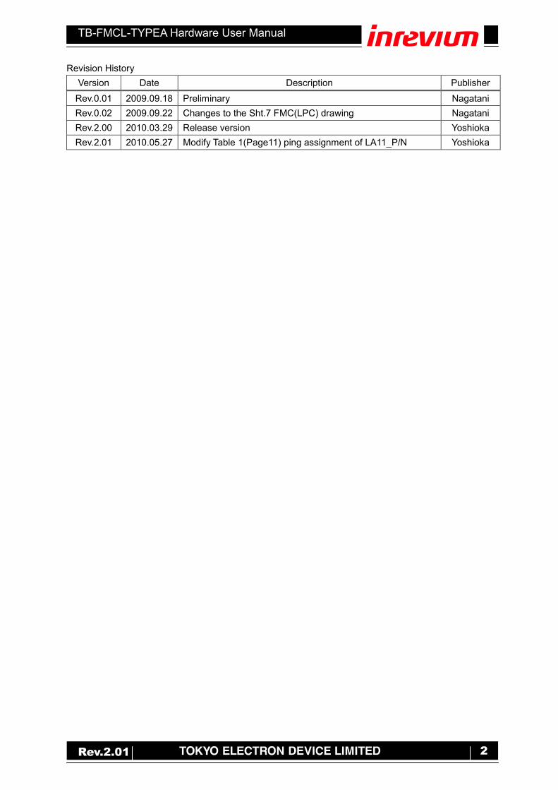
Revision History
Version Date Description Publisher
Rev.0.01 2009.09.18 Preliminary Nagatani
Rev.0.02 2009.09.22 Changes to the Sht.7 FMC(LPC) drawing Nagatani
Rev.2.00 2010.03.29 Release version Yoshioka
Rev.2.01 2010.05.27 Modify Table 1(Page11) ping assignment of LA11_P/N Yoshioka
TB-FMCL-TYPEA Hardware User Manual
3 Rev.2.01
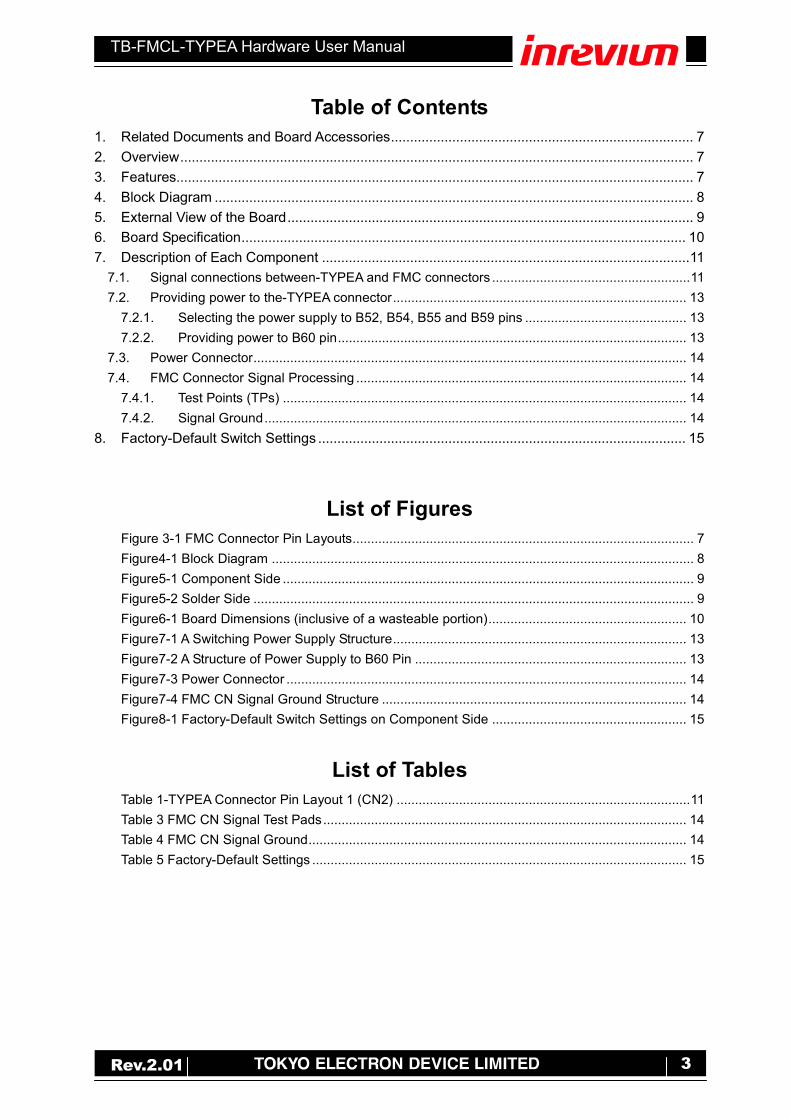
Table of Contents
1. Related Documents and Board Accessories............................................................................... 7
2. Overview...................................................................................................................................... 7
3. Features....................................................................................................................................... 7
4. Block Diagram ............................................................................................................................. 8
5. External View of the Board.......................................................................................................... 9
6. Board Specification.................................................................................................................... 10
7. Description of Each Component ................................................................................................11
7.1. Signal connections between-TYPEA and FMC connectors ......................................................11
7.2. Providing power to the-TYPEA connector................................................................................ 13
7.2.1. Selecting the power supply to B52, B54, B55 and B59 pins ............................................ 13
7.2.2. Providing power to B60 pin............................................................................................... 13
7.3. Power Connector...................................................................................................................... 14
7.4. FMC Connector Signal Processing .......................................................................................... 14
7.4.1. Test Points (TPs) .............................................................................................................. 14
7.4.2. Signal Ground................................................................................................................... 14
8. Factory-Default Switch Settings ................................................................................................ 15
List of Figures
Figure 3-1 FMC Connector Pin Layouts............................................................................................. 7
Figure4-1 Block Diagram ................................................................................................................... 8
Figure5-1 Component Side ................................................................................................................ 9
Figure5-2 Solder Side ........................................................................................................................ 9
Figure6-1 Board Dimensions (inclusive of a wasteable portion)...................................................... 10
Figure7-1 A Switching Power Supply Structure................................................................................ 13
Figure7-2 A Structure of Power Supply to B60 Pin .......................................................................... 13
Figure7-3 Power Connector ............................................................................................................. 14
Figure7-4 FMC CN Signal Ground Structure ................................................................................... 14
Figure8-1 Factory-Default Switch Settings on Component Side ..................................................... 15
List of Tables
Table 1-TYPEA Connector Pin Layout 1 (CN2) ................................................................................11
Table 3 FMC CN Signal Test Pads................................................................................................... 14
Table 4 FMC CN Signal Ground....................................................................................................... 14
Table 5 Factory-Default Settings ...................................................................................................... 15
TB-FMCL-TYPEA Hardware User Manual
4 Rev.2.01
Introduction Thank you for purchasing the TB-FMCL-TYPEA board.
Before using the product, be sure to carefully read this User Manual and fully understand how to
correctly use the product.
Read through this manual and always keep it handy.
Safety Precautions Be sure to observe these precautions
Observe the precautions listed below to prevent injuries to you or other personnel or damage to property.
• Before using the product, read these safety precautions carefully to assure correct use.
• These precautions contain serious safety instructions that must be observed.
• After reading through this manual, be sure to always keep it handy.
The following conventions are used to indicate and classify precautions in this manual. Failure to
observe precautions can result in injury to people or damage to property.
Indicates the high possibility of serious injury or death if the product is handled
incorrectly.
Indicates the possibility of serious injury or death if the product is handled
incorrectly.
Indicates the possibility of injury or physical damage in connection with houses or
household goods if the product is handled incorrectly.
The following graphical symbols are used to indicate and classify precautions in this manual.
(Examples)
Be sure to turn off the power switch.
Do not disassemble the product.
Do not attempt this.
Danger
Warning
Caution
!
TB-FMCL-TYPEA Hardware User Manual
5 Rev.2.01
In the event of a failure, disconnect the power supply.
If the product is used as is, a fire or electric shock may occur. Disconnect the power supply
immediately and contact our sales personnel for repair.
If an unpleasant smell or smoking occurs, disconnect the power supply.
If the product is used as is, a fire or electric shock may occur. Disconnect the power supply
immediately. After verifying that no smoking is observed, contact our sales personnel for
repair.
Do not disassemble, repair or modify the product.
Otherwise, a fire or electric shock may occur due to a short circuit or heat generation. For
inspection, modification or repair, contact our sales personnel.
Do not touch a cooling fan (when installing it).
As a cooling fan rotates in high speed, do not put your hand close to it. Otherwise, it may
cause injury to persons. Never touch a rotating cooling fan.
Do not place the product on unstable locations.
Otherwise, it may drop or fall, resulting in injury to persons or failure.
If the product is dropped or damaged, do not use it as is.
Otherwise, a fire or electric shock may occur.
Do not touch the product with a metallic object.
Otherwise, a fire or electric shock may occur.
Do not place the product in dusty or humid locations or where water may
splash.
Otherwise, a fire or electric shock may occur.
Do not get the product wet or touch it with a wet hand.
Otherwise, the product may break down or it may cause a fire, smoking or electric shock.
Do not touch a connector (gold-plated portion) on the product.
Otherwise, the surface of a connector may be contaminated with sweat or skin oil, resulting
in contact failure of a connector or it may cause a malfunction, fire or electric shock due to
static electricity.
Warning
!
!
!
!
!
!
!
TB-FMCL-TYPEA Hardware User Manual
6 Rev.2.01
Do not use or place the product in the following locations.
• Humid and dusty locations
• Airless locations such as closet or bookshelf
• Locations which receive oily smoke or steam
• Locations exposed to direct sunlight
• Locations close to heating equipment
• Closed inside of a car where the temperature becomes high
• Staticky locations
• Locations close to water or chemicals
Otherwise, a fire, electric shock, accident or deformation may occur due to a short circuit or heat
generation.
Do not place heavy things on the product.
Otherwise, the product may be damaged.
■ Disclaimer
This product is a board intended for conversion between the Samtec FMC connector and the Samtec
QTH series connector and can achieve gigabit transfer speeds. Tokyo Electron Device Limited
assumes no responsibility for any damages resulting from the use of this product for purposes other than
those stated.
Even if the product is used properly, Tokyo Electron Device Limited assumes no responsibility for any
damages caused by:
- Earthquake, thunder, natural disaster or fire resulting from the use beyond our responsibility, acts by a
third party or other accidents, the customer’s willful or accidental misuse or use under other abnormal
conditions,
- Secondary impact arising from use of this product or its unusable state (business interruption or
others),
- Use of this product against the instructions given in this manual or
- Malfunctions due to connection to other devices.
Tokyo Electron Device Limited assumes no responsibility or liability for:
- Erasure or corruption of data arising from use of this product
- Any consequences or other abnormalities arising from use of this product, or
- Damage of this product not due to our responsibility or failure due to modification
This product has been developed by assuming its use for research, testing or evaluation. It is not
authorized for use in any system or application that requires high reliability.
Repair of this product is carried out by replacing it on a chargeable basis, not repairing the faulty devices.
However, non-chargeable replacement is offered for initial failure if such notification is received within
two weeks after delivery of the product.
The specification of this product is subject to change without prior notice.
The product is subject to discontinuation without prior notice.
Caution
!
!
TB-FMCL-TYPEA Hardware User Manual
7 Rev.2.01
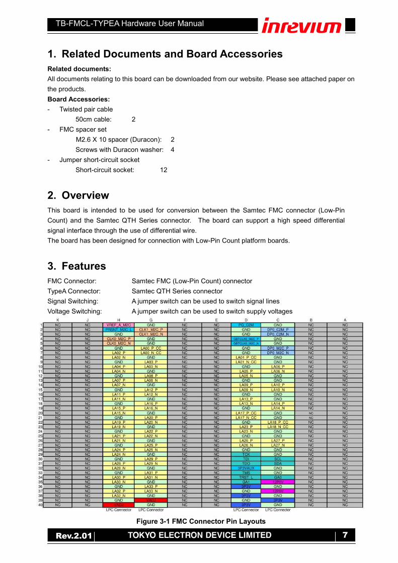
1. Related Documents and Board Accessories
Related documents:
All documents relating to this board can be downloaded from our website. Please see attached paper on
the products.
Board Accessories:
- Twisted pair cable
50cm cable: 2
- FMC spacer set
M2.6 X 10 spacer (Duracon): 2
Screws with Duracon washer: 4
- Jumper short-circuit socket
Short-circuit socket: 12
2. Overview
This board is intended to be used for conversion between the Samtec FMC connector (Low-Pin
Count) and the Samtec QTH Series connector. The board can support a high speed differential
signal interface through the use of differential wire.
The board has been designed for connection with Low-Pin Count platform boards.
3. Features
FMC Connector: Samtec FMC (Low-Pin Count) connector
TypeA Connector: Samtec QTH Series connector
Signal Switching: A jumper switch can be used to switch signal lines
Voltage Switching: A jumper switch can be used to switch supply voltages
Figure 3-1 FMC Connector Pin Layouts
TB-FMCL-TYPEA Hardware User Manual
8 Rev.2.01
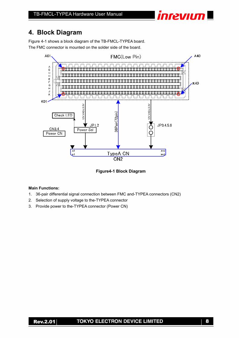
4. Block Diagram
Figure 4-1 shows a block diagram of the TB-FMCL-TYPEA board.
The FMC connector is mounted on the solder side of the board.
Figure4-1 Block Diagram
Main Functions:
1. 36-pair differential signal connection between FMC and-TYPEA connectors (CN2)
2. Selection of supply voltage to the-TYPEA connector
3. Provide power to the-TYPEA connector (Power CN)
36P
air(
72pi
n)
12V
,VA
DJ,3
.3V
12V
,VA
DJ,3
.3V
TB-FMCL-TYPEA Hardware User Manual
9 Rev.2.01
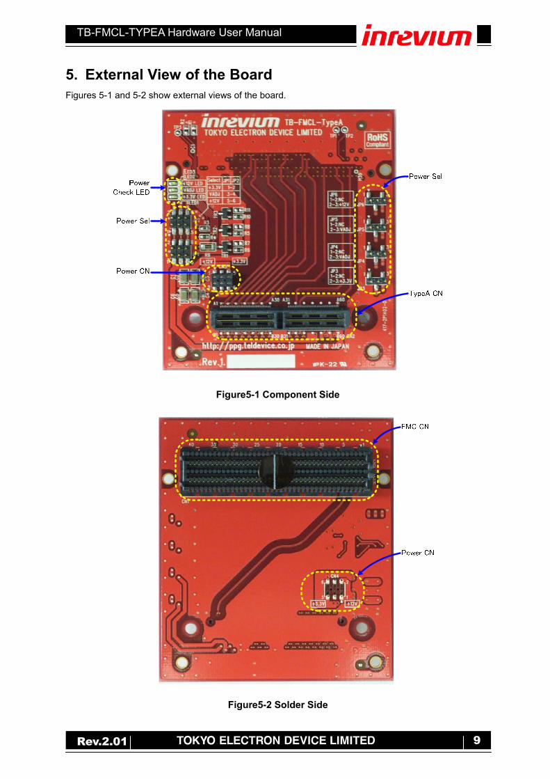
5. External View of the Board
Figures 5-1 and 5-2 show external views of the board.
Figure5-1 Component Side
Figure5-2 Solder Side
TB-FMCL-TYPEA Hardware User Manual
10 Rev.2.01
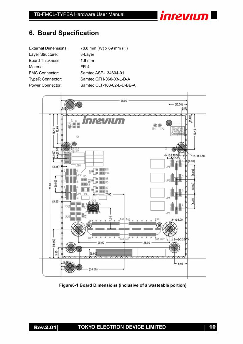
6. Board Specification
External Dimensions: 78.8 mm (W) x 69 mm (H)
Layer Structure: 8-Layer
Board Thickness: 1.6 mm
Material: FR-4
FMC Connector: Samtec ASP-134604-01
TypeR Connector: Samtec QTH-060-03-L-D-A
Power Connector: Samtec CLT-103-02-L-D-BE-A
Figure6-1 Board Dimensions (inclusive of a wasteable portion)
TB-FMCL-TYPEA Hardware User Manual
11 Rev.2.01
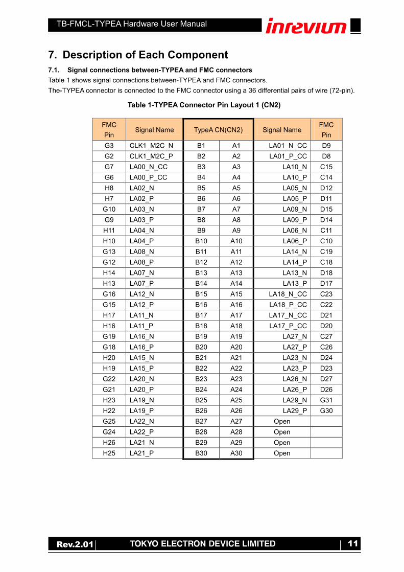
7. Description of Each Component
7.1. Signal connections between-TYPEA and FMC connectors
Table 1 shows signal connections between-TYPEA and FMC connectors.
The-TYPEA connector is connected to the FMC connector using a 36 differential pairs of wire (72-pin).
Table 1-TYPEA Connector Pin Layout 1 (CN2)
FMC
Pin Signal Name TypeA CN(CN2) Signal Name
FMC
Pin
G3 CLK1_M2C_N B1 A1 LA01_N_CC D9
G2 CLK1_M2C_P B2 A2 LA01_P_CC D8
G7 LA00_N_CC B3 A3 LA10_N C15
G6 LA00_P_CC B4 A4 LA10_P C14
H8 LA02_N B5 A5 LA05_N D12
H7 LA02_P B6 A6 LA05_P D11
G10 LA03_N B7 A7 LA09_N D15
G9 LA03_P B8 A8 LA09_P D14
H11 LA04_N B9 A9 LA06_N C11
H10 LA04_P B10 A10 LA06_P C10
G13 LA08_N B11 A11 LA14_N C19
G12 LA08_P B12 A12 LA14_P C18
H14 LA07_N B13 A13 LA13_N D18
H13 LA07_P B14 A14 LA13_P D17
G16 LA12_N B15 A15 LA18_N_CC C23
G15 LA12_P B16 A16 LA18_P_CC C22
H17 LA11_N B17 A17 LA17_N_CC D21
H16 LA11_P B18 A18 LA17_P_CC D20
G19 LA16_N B19 A19 LA27_N C27
G18 LA16_P B20 A20 LA27_P C26
H20 LA15_N B21 A21 LA23_N D24
H19 LA15_P B22 A22 LA23_P D23
G22 LA20_N B23 A23 LA26_N D27
G21 LA20_P B24 A24 LA26_P D26
H23 LA19_N B25 A25 LA29_N G31
H22 LA19_P B26 A26 LA29_P G30
G25 LA22_N B27 A27 Open
G24 LA22_P B28 A28 Open
H26 LA21_N B29 A29 Open
H25 LA21_P B30 A30 Open
TB-FMCL-TYPEA Hardware User Manual
12 Rev.2.01
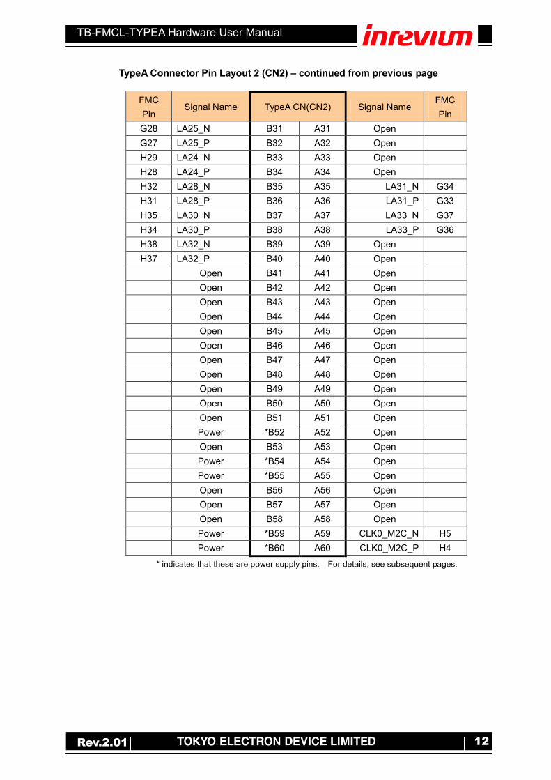
TypeA Connector Pin Layout 2 (CN2) – continued from previous page
FMC
Pin Signal Name TypeA CN(CN2) Signal Name
FMC
Pin
G28 LA25_N B31 A31 Open
G27 LA25_P B32 A32 Open
H29 LA24_N B33 A33 Open
H28 LA24_P B34 A34 Open
H32 LA28_N B35 A35 LA31_N G34
H31 LA28_P B36 A36 LA31_P G33
H35 LA30_N B37 A37 LA33_N G37
H34 LA30_P B38 A38 LA33_P G36
H38 LA32_N B39 A39 Open
H37 LA32_P B40 A40 Open
Open B41 A41 Open
Open B42 A42 Open
Open B43 A43 Open
Open B44 A44 Open
Open B45 A45 Open
Open B46 A46 Open
Open B47 A47 Open
Open B48 A48 Open
Open B49 A49 Open
Open B50 A50 Open
Open B51 A51 Open
Power *B52 A52 Open
Open B53 A53 Open
Power *B54 A54 Open
Power *B55 A55 Open
Open B56 A56 Open
Open B57 A57 Open
Open B58 A58 Open
Power *B59 A59 CLK0_M2C_N H5
Power *B60 A60 CLK0_M2C_P H4
* indicates that these are power supply pins. For details, see subsequent pages.
TB-FMCL-TYPEA Hardware User Manual
13 Rev.2.01
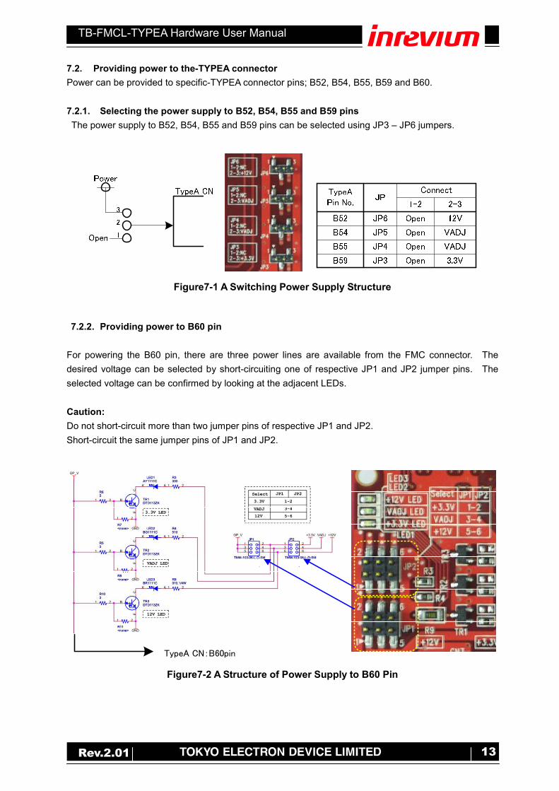
7.2. Providing power to the-TYPEA connector
Power can be provided to specific-TYPEA connector pins; B52, B54, B55, B59 and B60.
7.2.1. Selecting the power supply to B52, B54, B55 and B59 pins
The power supply to B52, B54, B55 and B59 pins can be selected using JP3 – JP6 jumpers.
Figure7-1 A Switching Power Supply Structure
7.2.2. Providing power to B60 pin
For powering the B60 pin, there are three power lines are available from the FMC connector. The
desired voltage can be selected by short-circuiting one of respective JP1 and JP2 jumper pins. The
selected voltage can be confirmed by looking at the adjacent LEDs.
Caution:
Do not short-circuit more than two jumper pins of respective JP1 and JP2.
Short-circuit the same jumper pins of JP1 and JP2.
Figure7-2 A Structure of Power Supply to B60 Pin
TypeA CN:B60pin
TB-FMCL-TYPEA Hardware User Manual
14 Rev.2.01
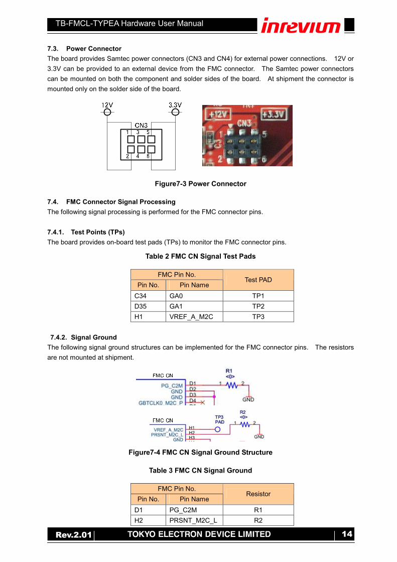
7.3. Power Connector
The board provides Samtec power connectors (CN3 and CN4) for external power connections. 12V or
3.3V can be provided to an external device from the FMC connector. The Samtec power connectors
can be mounted on both the component and solder sides of the board. At shipment the connector is
mounted only on the solder side of the board.
Figure7-3 Power Connector
7.4. FMC Connector Signal Processing
The following signal processing is performed for the FMC connector pins.
7.4.1. Test Points (TPs)
The board provides on-board test pads (TPs) to monitor the FMC connector pins.
Table 2 FMC CN Signal Test Pads
FMC Pin No.
Pin No. Pin Name Test PAD
C34 GA0 TP1
D35 GA1 TP2
H1 VREF_A_M2C TP3
7.4.2. Signal Ground
The following signal ground structures can be implemented for the FMC connector pins. The resistors
are not mounted at shipment.
Figure7-4 FMC CN Signal Ground Structure
Table 3 FMC CN Signal Ground
FMC Pin No.
Pin No. Pin Name Resistor
D1 PG_C2M R1
H2 PRSNT_M2C_L R2
TB-FMCL-TYPEA Hardware User Manual
15 Rev.2.01
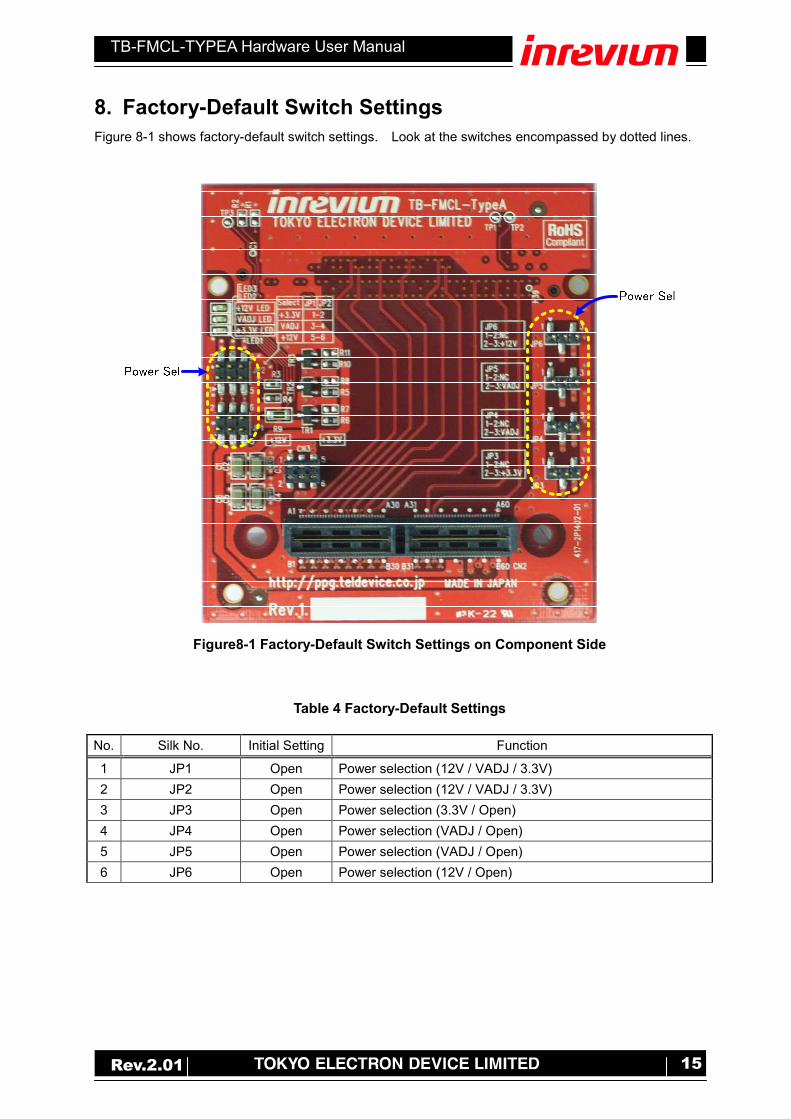
8. Factory-Default Switch Settings
Figure 8-1 shows factory-default switch settings. Look at the switches encompassed by dotted lines.
Figure8-1 Factory-Default Switch Settings on Component Side
Table 4 Factory-Default Settings
No. Silk No. Initial Setting Function
1 JP1 Open Power selection (12V / VADJ / 3.3V)
2 JP2 Open Power selection (12V / VADJ / 3.3V)
3 JP3 Open Power selection (3.3V / Open)
4 JP4 Open Power selection (VADJ / Open)
5 JP5 Open Power selection (VADJ / Open)
6 JP6 Open Power selection (12V / Open)

TB-FMCL-TYPEA Hardware User Manual
16 Rev.2.01
PLD Solution Division URL: http://www.inrevium.jp/eng/x-fpga-board/ E-mail: [email protected] HEAD Quarter : Yokohama East Square, 1-4 Kinko-cho, Kanagawa-ku, Yokohama City,
Kanagawa, Japan 221-0056 TEL:+81-45-443-4016 FAX:+81-45-443-4058


![arXiv:1609.04437v1 [math.NA] 14 Sep 2016that the ad hoc norm may not be appropriate for problem (1.1), and proposed a residual-typea posteriori estimator for 1D convection-diffusion](https://img.pdfslide.net/doc/110x75/613360badfd10f4dd73b0c87/arxiv160904437v1-mathna-14-sep-2016-that-the-ad-hoc-norm-may-not-be-appropriate.jpg)