Embed Size (px)
Citation preview
by MC68HC912BC32TS/DMOTOROLASEMICONDUCTOR
TECHNICAL DATAMC68HC912BC32
Technical Summary16-Bit Microcontroller
1 IntroductionThe MC68HC912BC32 microcontroller unit (MCU) is a16-bit device composed of standard on-chip pe-ripherals including a 16-bit central processing unit (CPU12), 32-Kbyte flash EEPROM, 1-Kbyte RAM,768-byte EEPROM, an asynchronous serial communications interface (SCI), a serial peripheral inter-face (SPI), an 8-channel timer and 16-bit pulse accumulator, an 10-bit analog-to-digital converter(ADC), a four-channel pulse-width modulator (PWM), and a CAN 2.0B compatible controller(MSCAN12). System resource mapping, clock generation, interrupt control and bus interfacing aremanaged by the Lite integration module (LIM). The MC68HC912BC32 has full 16-bit data pathsthroughout, however, the multiplexed external bus can operate in an 8-bit narrow mode so single 8-bitwide memory can be interfaced for lower cost systems.
1.1 Features• 16-Bit CPU12
— Upward Compatible with M68HC11 Instruction Set— Interrupt Stacking and Programmer’s Model Identical to M68HC11— 20-Bit ALU— Instruction Queue— Enhanced Indexed Addressing— Fuzzy Logic Instructions
• Multiplexed Bus— Single Chip or Expanded— 16/16 Wide or 16/8 Narrow Modes
• Memory— 32-Kbyte Flash EEPROM with 2-Kbyte Erase-Protected Boot Block— 768-byte EEPROM— 1-Kbyte RAM with Single-Cycle Access for Aligned or Misaligned Read/Write
• 8-Channel, 10-Bit Analog-to-Digital Converter• 8-Channel Timer
— Each Channel Fully Configurable as Either Input Capture or Output Compare— Simple PWM Mode— Modulo Reset of Timer Counter
• 16-Bit Pulse Accumulator— External Event Counting— Gated Time Accumulation
• Pulse-Width Modulator
This document contains information on a new product. Specifications and information herein are subject to change without notice.
© MOTOROLA INC., 1997 Rev. 2.0
— 8-Bit, 4-Channel or 16-Bit, 2-Channel
— Separate Control for Each Pulse Width and Duty Cycle— Programmable Center-Aligned or Left-Aligned Outputs
• Serial Interfaces— Asynchronous Serial Communications Interface (SCI)— Synchronous Serial Peripheral Interface (SPI)
• Motorola Scalable CAN Controller (MSCAN12)— CAN 2.0B compatible (standard and extended identifiers)— Two receive and three transmit buffers— Flexible identifier filter programmable as 2 x 32 bit, 4 x 16 bit, or 8 x 8 bit— Four separate interrupt channels for Rx, Tx, error and wake-up— Low-pass filter wake-up function— Loop-back mode for self test operation
• COP Watchdog Timer, Clock Monitor, and Periodic Interrupt Timer• 80-Pin QFP Package
— Up to 63 General-Purpose I/O Lines— 4.5V–5.5V Operation at 8 MHz
• Single-Wire Background Debug™ Mode (BDM)• On-Chip Hardware Breakpoints
1.2 Ordering Information
The MC68HC912BC32 is packaged in 80-pin quad flat pack (QFP) packaging and is shipped in two-piece sample packs, 50-piece trays, or 250-piece bricks. Operating temperature range and voltage re-quirements are specified when ordering the MC68HC912BC32 device. Refer to Table 1 for part num-bers.
NOTE: This part is also available in 2-piece sample packs and 250-piece bricks.
Evaluation boards, assemblers, compilers, and debuggers are available from Motorola and from third-party suppliers. An up-to-date list of products that support the M68HC12 family of microcontrollers canbe found on the World Wide Web at the following URL:
http://www.mcu.motsps.com
Documents to assist in product selection are available from the Motorola Literature Distribution Centeror your local Motorola Sales Office:
AMCU Device Selection Guide (SG166/D)
AMCU Software and Development Tool Selector Guide (SG176/D)
Table 1 MC68HC912BC32 Device Ordering Information
Order NumberTemperature
Voltage Frequency PackageRange Designator
MC68HC912BC32FU8 0 to +70 °C4.5V–5.5V 8 MHz
80-Pin QFPSingle Tray
50 PcsMC68HC912BC32CFU8 −40 to +85 °C C
MOTOROLA Introduction MC68HC912BC322 MC68HC912BC32TS/D
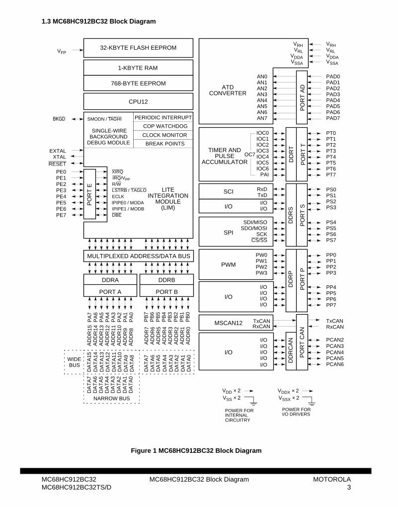
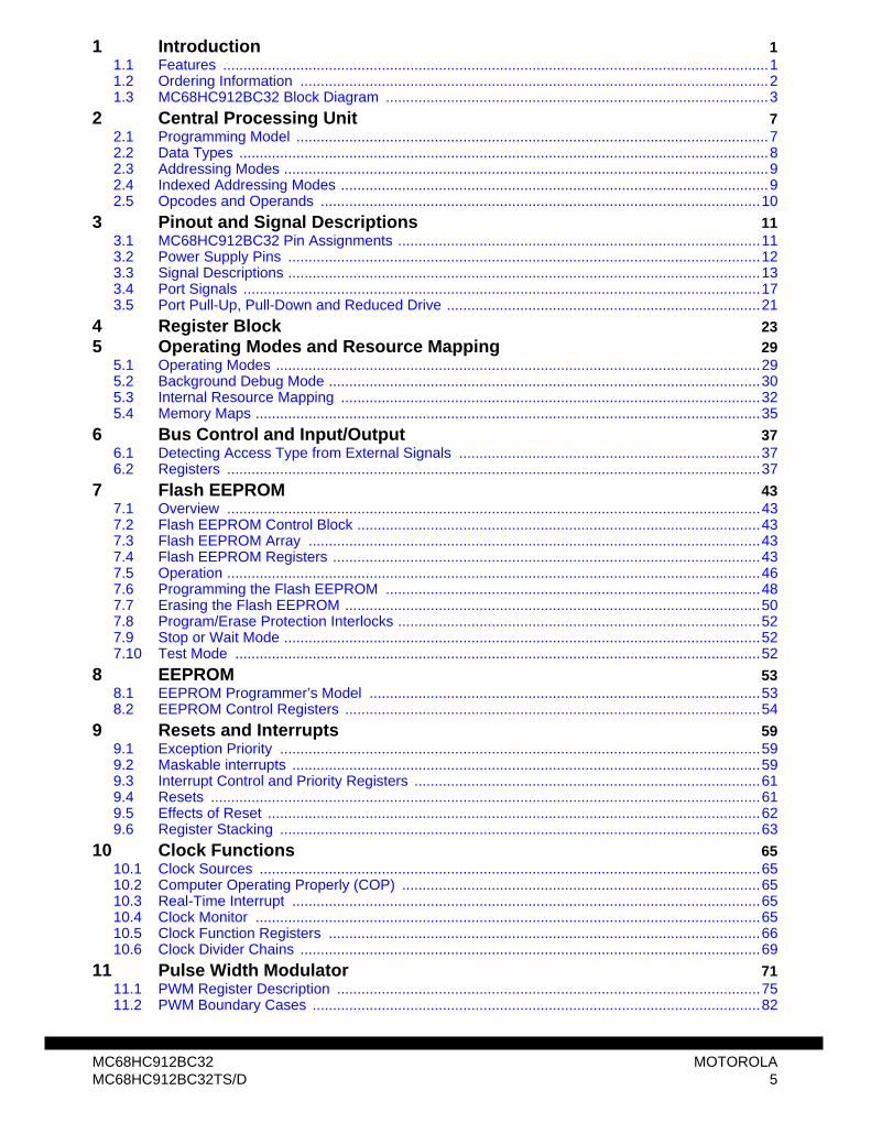
1.3 MC68HC912BC32 Block Diagram
IOC0IOC1IOC2IOC3IOC4IOC5IOC6
PAI
OC7
DD
RT
PO
RT
T
PERIODIC INTERRUPT
COP WATCHDOG
32-KBYTE FLASH EEPROM
1-KBYTE RAM
PO
RT
E
TIMER AND
PT0PT1PT2PT3PT4PT5PT6PT7
SPI
DD
RS
PO
RT
S
ATD
PO
RT
AD
PE1PE2
PE4PE5PE6
PE3
PAD3PAD4PAD5PAD6PAD7
VDDAVSSA
VRHVRL
PAD0PAD1PAD2
DDRA
PORT A
DDRB
PORT B
PA
4P
A3
PA
2P
A1
PA
0
PA
7P
A6
PA
5
PB
4P
B3
PB
2P
B1
PB
0
PB
7P
B6
PB
5
DA
TA
15
MULTIPLEXED ADDRESS/DATA BUS
RESET
EXTALXTAL
PW0PW1PW2PW3
PWM
DD
RP
PO
RT
P
PP0PP1PP2PP3
VDD × 2VSS × 2
SCI RxDTxDI/OI/O
SDI/MISOSDO/MOSI
SCKCS/SS
PS0PS1PS2PS3
PS4PS5PS6PS7
768-BYTE EEPROM
CLOCK MONITOR
PE0
PE7
AN3AN4AN5AN6AN7
VDDAVSSA
VRHVRL
AN0AN1AN2
SINGLE-WIREBACKGROUND
DEBUG MODULE
SMODN / TAGHI
ECLK
R/WLSTRB / TAGLO
IPIPE0 / MODAIPIPE1 / MODB
XIRQ
DBE
PULSEACCUMULATOR
LITE
IRQ/VPP
PP4PP5PP6PP7
I/OI/OI/OI/O
I/O
I/O
RxCANTxCAN
I/O
MSCAN12
DD
RC
AN
PO
RT
CA
N
PCAN4PCAN5PCAN6
I/OI/OI/O
I/O
TxCANRxCAN
PCAN2PCAN3
INTEGRATIONMODULE
(LIM)
VFP
BREAK POINTS
CPU12
AD
DR
15A
DD
R14
AD
DR
13A
DD
R12
AD
DR
11A
DD
R10
AD
DR
9A
DD
R8
DA
TA
14D
AT
A13
DA
TA
12D
AT
A11
DA
TA
10D
AT
A9
DA
TA
8
AD
DR
7A
DD
R6
AD
DR
5A
DD
R4
AD
DR
3A
DD
R2
AD
DR
1A
DD
R0
DA
TA
7D
AT
A6
DA
TA
5D
AT
A4
DA
TA
3D
AT
A2
DA
TA
1D
AT
A0
I/O
CONVERTER
VSSX × 2VDDX × 2
POWER FORPOWER FORI/O DRIVERSINTERNAL
CIRCUITRY
DA
TA
7D
AT
A6
DA
TA
5D
AT
A4
DA
TA
3D
AT
A2
DA
TA
1D
AT
A0
NARROW BUS
WIDEBUS
BKGD
MC68HC912BC32 MC68HC912BC32 Block Diagram MOTOROLAMC68HC912BC32TS/D 3
Figure 1 MC68HC912BC32 Block Diagram

MOTOROLA MC68HC912BC32 Block Diagram MC68HC912BC324 MC68HC912BC32TS/D
1 Introduction 11.1 Features ......................................................................................................................................11.2 Ordering Information ...................................................................................................................21.3 MC68HC912BC32 Block Diagram ..............................................................................................3
2 Central Processing Unit 72.1 Programming Model ....................................................................................................................72.2 Data Types ..................................................................................................................................82.3 Addressing Modes .......................................................................................................................92.4 Indexed Addressing Modes .........................................................................................................92.5 Opcodes and Operands ............................................................................................................10
3 Pinout and Signal Descriptions 113.1 MC68HC912BC32 Pin Assignments .........................................................................................113.2 Power Supply Pins ....................................................................................................................123.3 Signal Descriptions ....................................................................................................................133.4 Port Signals ...............................................................................................................................173.5 Port Pull-Up, Pull-Down and Reduced Drive .............................................................................21
4 Register Block 235 Operating Modes and Resource Mapping 29
5.1 Operating Modes .......................................................................................................................295.2 Background Debug Mode ..........................................................................................................305.3 Internal Resource Mapping .......................................................................................................325.4 Memory Maps ............................................................................................................................35
6 Bus Control and Input/Output 376.1 Detecting Access Type from External Signals ..........................................................................376.2 Registers ...................................................................................................................................37
7 Flash EEPROM 437.1 Overview ...................................................................................................................................437.2 Flash EEPROM Control Block ...................................................................................................437.3 Flash EEPROM Array ...............................................................................................................437.4 Flash EEPROM Registers .........................................................................................................437.5 Operation ...................................................................................................................................467.6 Programming the Flash EEPROM ............................................................................................487.7 Erasing the Flash EEPROM ......................................................................................................507.8 Program/Erase Protection Interlocks .........................................................................................527.9 Stop or Wait Mode .....................................................................................................................527.10 Test Mode .................................................................................................................................52
8 EEPROM 538.1 EEPROM Programmer’s Model ................................................................................................538.2 EEPROM Control Registers ......................................................................................................54
9 Resets and Interrupts 599.1 Exception Priority ......................................................................................................................599.2 Maskable interrupts ...................................................................................................................599.3 Interrupt Control and Priority Registers .....................................................................................619.4 Resets .......................................................................................................................................619.5 Effects of Reset .........................................................................................................................629.6 Register Stacking ......................................................................................................................63
10 Clock Functions 6510.1 Clock Sources ...........................................................................................................................6510.2 Computer Operating Properly (COP) ........................................................................................6510.3 Real-Time Interrupt ...................................................................................................................6510.4 Clock Monitor ............................................................................................................................6510.5 Clock Function Registers ..........................................................................................................6610.6 Clock Divider Chains .................................................................................................................69
11 Pulse Width Modulator 7111.1 PWM Register Description ........................................................................................................75
MC68HC912BC32 MOTOROLAMC68HC912BC32TS/D 5
11.2 PWM Boundary Cases ..............................................................................................................82
12 Standard Timer Module 8312.1 Timer Registers .........................................................................................................................8412.2 Timer Operation in Modes .........................................................................................................92
13 Serial Interface 9313.1 Block diagram ............................................................................................................................9313.2 Serial Communication Interface (SCI) .......................................................................................9313.3 Serial Peripheral Interface (SPI) ..............................................................................................10013.4 Port S ......................................................................................................................................106
14 MSCAN12 Controller 10914.1 Features ..................................................................................................................................10914.2 External Pins ...........................................................................................................................11014.3 Message Storage ....................................................................................................................11114.4 Identifier Acceptance Filter ......................................................................................................11414.5 Interrupts .................................................................................................................................11714.6 Protocol Violation Protection ...................................................................................................11914.7 Low Power Modes ...................................................................................................................11914.8 Timer Link ................................................................................................................................12214.9 Clock System ..........................................................................................................................12214.10 Memory Map ...........................................................................................................................12414.11 Programmer’s Model of Message Storage ..............................................................................12514.12 Programmer’s Model of Control Registers ..............................................................................129
15 Analog-To-Digital Converter 14315.1 Functional Description .............................................................................................................14315.2 ATD Registers .........................................................................................................................14415.3 ATD Mode Operation ..............................................................................................................150
16 Development Support 15116.1 Instruction Queue ....................................................................................................................15116.2 Background Debug Mode ........................................................................................................15216.3 Breakpoints .............................................................................................................................16116.4 Instruction Tagging ..................................................................................................................165
17 Summary of Changes 167
MOTOROLA MC68HC912BC326 MC68HC912BC32TS/D
2 Central Processing UnitThe CPU12 is a high-speed, 16-bit processing unit. It has full 16-bit data paths and wider internal reg-isters (up to 20 bits) for high-speed extended math instructions. The instruction set is a proper supersetof the M68HC11instruction set. The CPU12 allows instructions with odd byte counts, including manysingle-byte instructions. This provides efficient use of ROM space. An instruction queue buffers pro-gram information so the CPU always has immediate access to at least three bytes of machine code atthe start of every instruction. The CPU12 also offers an extensive set of indexed addressing capabilities.
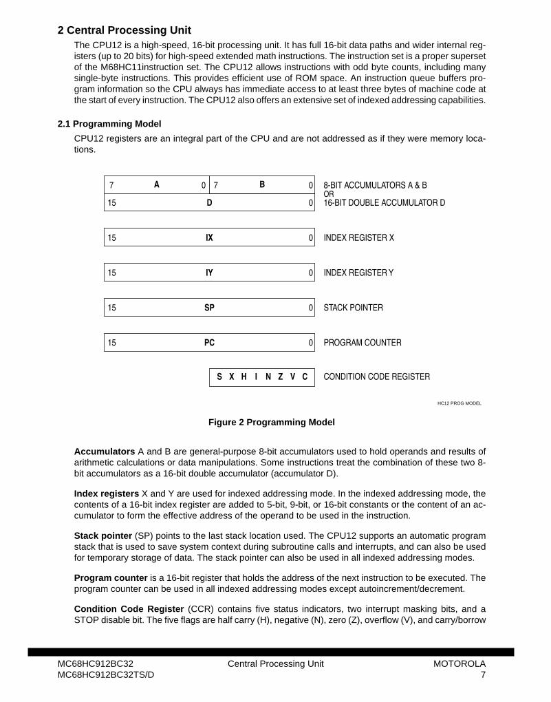
2.1 Programming Model
CPU12 registers are an integral part of the CPU and are not addressed as if they were memory loca-tions.
Figure 2 Programming Model
Accumulators A and B are general-purpose 8-bit accumulators used to hold operands and results ofarithmetic calculations or data manipulations. Some instructions treat the combination of these two 8-bit accumulators as a 16-bit double accumulator (accumulator D).
Index registers X and Y are used for indexed addressing mode. In the indexed addressing mode, thecontents of a 16-bit index register are added to 5-bit, 9-bit, or 16-bit constants or the content of an ac-cumulator to form the effective address of the operand to be used in the instruction.
Stack pointer (SP) points to the last stack location used. The CPU12 supports an automatic programstack that is used to save system context during subroutine calls and interrupts, and can also be usedfor temporary storage of data. The stack pointer can also be used in all indexed addressing modes.
Program counter is a 16-bit register that holds the address of the next instruction to be executed. Theprogram counter can be used in all indexed addressing modes except autoincrement/decrement.
Condition Code Register (CCR) contains five status indicators, two interrupt masking bits, and a
7
15
15
15
15
15
D
IX
IY
SP
PC
A B
NS X H I Z V C
0
0
0
0
0
0
70
CONDITION CODE REGISTER
8-BIT ACCUMULATORS A & B
16-BIT DOUBLE ACCUMULATOR D
INDEX REGISTER X
INDEX REGISTER Y
STACK POINTER
PROGRAM COUNTER
OR
HC12 PROG MODEL
MC68HC912BC32 Central Processing Unit MOTOROLAMC68HC912BC32TS/D 7
STOP disable bit. The five flags are half carry (H), negative (N), zero (Z), overflow (V), and carry/borrow
(C). The half-carry flag is used only for BCD arithmetic operations. The N, Z, V, and C status bits allowfor branching based on the results of a previous operation.
2.2 Data Types
The CPU12 supports the following data types:
• Bit data• 8-bit and 16-bit signed and unsigned integers• 16-bit unsigned fractions• 16-bit addresses
A byte is eight bits wide and can be accessed at any byte location. A word is composed of two consec-utive bytes with the most significant byte at the lower value address. There are no special requirementsfor alignment of instructions or operands.
MOTOROLA Central Processing Unit MC68HC912BC328 MC68HC912BC32TS/D
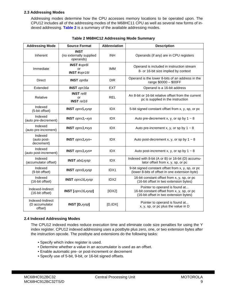
2.3 Addressing Modes
Addressing modes determine how the CPU accesses memory locations to be operated upon. TheCPU12 includes all of the addressing modes of the M68HC11 CPU as well as several new forms of in-dexed addressing. Table 2 is a summary of the available addressing modes.
2.4 Indexed Addressing Modes
The CPU12 indexed modes reduce execution time and eliminate code size penalties for using the Yindex register. CPU12 indexed addressing uses a postbyte plus zero, one, or two extension bytes afterthe instruction opcode. The postbyte and extensions do the following tasks:
• Specify which index register is used.• Determine whether a value in an accumulator is used as an offset.• Enable automatic pre- or post-increment or decrement• Specify use of 5-bit, 9-bit, or 16-bit signed offsets.
Table 2 M68HC12 Addressing Mode Summary
Addressing Mode Source Format Abbreviation Description
InherentINST
(no externally supplied operands)
INH Operands (if any) are in CPU registers
ImmediateINST #opr8i
orINST #opr16i
IMMOperand is included in instruction stream
8- or 16-bit size implied by context
Direct INST opr8a DIR Operand is the lower 8-bits of an address in the range $0000 – $00FF
Extended INST opr16a EXT Operand is a 16-bit address
RelativeINST rel8
orINST rel16
REL An 8-bit or 16-bit relative offset from the current pc is supplied in the instruction
Indexed(5-bit offset) INST oprx5,xysp IDX 5-bit signed constant offset from x, y, sp, or pc
Indexed(auto pre-decrement) INST oprx3,–xys IDX Auto pre-decrement x, y, or sp by 1 ~ 8
Indexed(auto pre-increment) INST oprx3,+xys IDX Auto pre-increment x, y, or sp by 1 ~ 8
Indexed(auto post-decrement)
INST oprx3,xys– IDX Auto post-decrement x, y, or sp by 1 ~ 8
Indexed(auto post-increment) INST oprx3,xys+ IDX Auto post-increment x, y, or sp by 1 ~ 8
Indexed(accumulator offset) INST abd,xysp IDX Indexed with 8-bit (A or B) or 16-bit (D) accumu-
lator offset from x, y, sp, or pc
Indexed(9-bit offset) INST oprx9,xysp IDX1 9-bit signed constant offset from x, y, sp, or pc
(lower 8-bits of offset in one extension byte)
Indexed(16-bit offset) INST oprx16,xysp IDX2 16-bit constant offset from x, y, sp, or pc
(16-bit offset in two extension bytes)
Indexed-Indirect(16-bit offset) INST [oprx16,xysp] [IDX2]
Pointer to operand is found at...16-bit constant offset from x, y, sp, or pc
(16-bit offset in two extension bytes)
Indexed-Indirect(D accumulator
offset)INST [D,xysp] [D,IDX] Pointer to operand is found at...
x, y, sp, or pc plus the value in D
MC68HC912BC32 Central Processing Unit MOTOROLAMC68HC912BC32TS/D 9
2.5 Opcodes and Operands
The CPU12 uses 8-bit opcodes. Each opcode identifies a particular instruction and associated address-ing mode to the CPU. Several opcodes are required to provide each instruction with a range of address-ing capabilities.
Only 256 opcodes would be available if the range of values were restricted to the number that can berepresented by 8-bit binary numbers. To expand the number of opcodes, a second page is added to theopcode map. Opcodes on the second page are preceded by an additional byte with the value $18.
To provide additional addressing flexibility, opcodes can also be followed by a postbyte or extensionbytes. Postbytes implement certain forms of indexed addressing, transfers, exchanges, and loop prim-itives. Extension bytes contain additional program information such as addresses, offsets, and immedi-ate data.
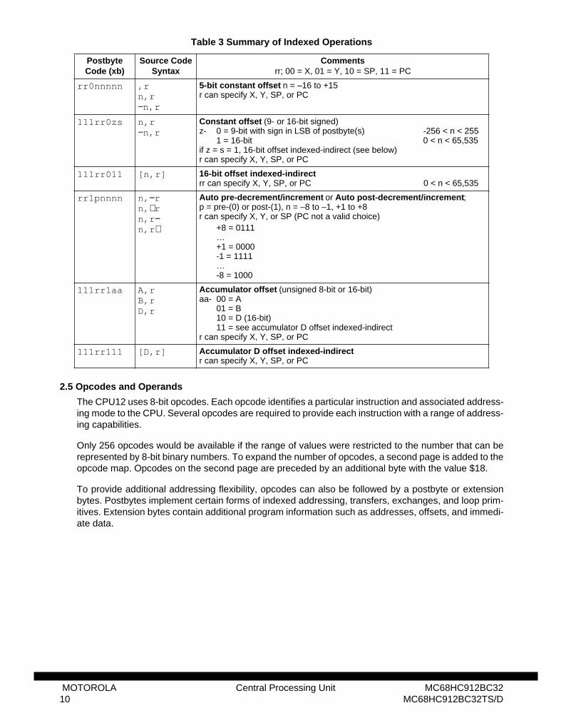
Table 3 Summary of Indexed Operations
PostbyteCode (xb)
Source CodeSyntax
Commentsrr; 00 = X, 01 = Y, 10 = SP, 11 = PC
rr0nnnnn ,rn,r−n,r
5-bit constant offset n = –16 to +15r can specify X, Y, SP, or PC
111rr0zs n,r−n,r
Constant offset (9- or 16-bit signed)z- 0 = 9-bit with sign in LSB of postbyte(s) -256 < n < 255
1 = 16-bit 0 < n < 65,535if z = s = 1, 16-bit offset indexed-indirect (see below)r can specify X, Y, SP, or PC
111rr011 [n,r] 16-bit offset indexed-indirectrr can specify X, Y, SP, or PC 0 < n < 65,535
rr1pnnnn n,−r n,+rn,r−n,r+
Auto pre-decrement/increment or Auto post-decrement/increment; p = pre-(0) or post-(1), n = –8 to –1, +1 to +8r can specify X, Y, or SP (PC not a valid choice)
+8 = 0111…+1 = 0000-1 = 1111…-8 = 1000
111rr1aa A,rB,rD,r
Accumulator offset (unsigned 8-bit or 16-bit)aa- 00 = A
01 = B10 = D (16-bit)11 = see accumulator D offset indexed-indirect
r can specify X, Y, SP, or PC
111rr111 [D,r] Accumulator D offset indexed-indirectr can specify X, Y, SP, or PC
MOTOROLA Central Processing Unit MC68HC912BC3210 MC68HC912BC32TS/D
3 Pinout and Signal Descriptions
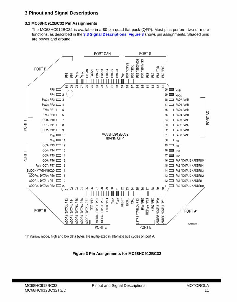
3.1 MC68HC912BC32 Pin Assignments
The MC68HC912BC32 is available in a 80-pin quad flat pack (QFP). Most pins perform two or morefunctions, as described in the 3.3 Signal Descriptions. Figure 3 shows pin assignments. Shaded pinsare power and ground.
Figure 3 Pin Assignments for MC68HC912BC32
MC68HC912BC3280-PIN QFP
HC12 80QFP
PP5
PP4
PW3 / PP3
PW2 / PP2
PW1/ PP1
41
1
2
3
4
5
6
7
8
9
10
11
12
13
14
15
16
17
18
19
20
4021 22 23 24 25 26 27 28 29 30 31 32 33 34 35 36 37 38 39
42
43
44
45
46
47
48
49
50
51
52
53
54
55
56
57
58
59
60
6162636465666768697071727374757677787980
PA2 / DATA10 / ADDR10
PA3 / DATA11 / ADDR11
PA4 / DATA12 / ADDR12
PA5 / DATA13 / ADDR13
PA6 / DATA14 / ADDR14
PA7 / DATA15 / ADDR15
PP6
PP7
ADDR0 / DATA0 / PB0
ADDR1 / DATA1 / PB1
ADDR2 / DATA2 / PB2
SMODN / TAGHI/ BKGD
PAI / IOC7 / PT7
IOC6 / PT6
IOC5 / PT5
IOC4 / PT4
IOC3 / PT3
IOC2 / PT2
IOC1 / PT1
IOC0 / PT0
ADD
R9
/ DAT
A9 /
PA1
XIR
Q /
PE0
IRQ
/VPP
/ PE
1
R/W
/ PE
2
LSTR
B / T
AGLO
/ PE
3
XTAL
EXTA
L
RES
ET
V DD
X
V SSX
ECLK
/ PE
4
MO
DA /
IPIP
E0 /
PE5
MO
DB
/ IPI
PE1
/ PE6
DBE
/ PE
7
ADD
R7
/ DAT
A7 /
PB7
ADD
R6
/ DAT
A6 /
PB6
ADD
R5
/ DAT
A5 /
PB5
ADD
R4
/ DAT
A4 /
PB4
ADD
R3
/ DAT
A3 /
PB3
VDD
VSS
PW0/ PP0
VSSA
VDDA
PAD7 / AN7
PAD6 / AN6
PAD5 / AN5
PAD4 / AN4
PAD3 / AN3
PAD2 / AN2
PAD1 / AN1
PAD0 / AN0
VRL
VRH
VSS
VDD
PS0
/ RxD
PS1
/ TxD
PS2
PS3
PS4
/ SD
I/MIS
O
PS5
/ SD
O/M
OSI
PS6
/ SC
K
PS7
/ CS /
SS
V FP
PCAN
6
PCAN
5
PCAN
4
PCAN
3
PCAN
2
TxC
AN
RxC
AN
V SSX
V DD
X
ADD
R8
/ DAT
A8 /
PA0
PORT
AD
PORT A*PORT B
PORT EPORT E
PORT CAN PORT S
PORT P
PORT
TPO
RT T
* In narrow mode, high and low data bytes are multiplexed in alternate bus cycles on port A.
MC68HC912BC32 Pinout and Signal Descriptions MOTOROLAMC68HC912BC32TS/D 11

3.2 Power Supply Pins
MC68HC912BC32 power and ground pins are described below and summarized in Table 4.
3.2.1 Internal Power (VDD) and Ground (VSS)
Power is supplied to the MCU through VDD and VSS. Because fast signal transitions place high, short-duration current demands on the power supply, use bypass capacitors with high-frequency character-istics and place them as close to the MCU as possible. Bypass requirements depend on how heavilythe MCU pins are loaded.
3.2.2 External Power (VDDX) and Ground (VSSX)
External power and ground for I/O drivers. Because fast signal transitions place high, short-duration cur-rent demands on the power supply, use bypass capacitors with high-frequency characteristics andplace them as close to the MCU as possible. Bypass requirements depend on how heavily the MCUpins are loaded.
3.2.3 VDDA, VSSA
Provides operating voltage and ground for the analog-to-digital converter. This allows the supply volt-age to the A/D to be bypassed independently.
3.2.4 Analog to Digital Reference Voltages (VRH, VRL)
3.2.5 VFP
Flash EEPROM programming voltage and supply voltage during normal operation.
3.2.6 VPP
High voltage supply to EEPROM. Used to monitor charge pump output and testing. Not intended forgeneral applications use.
Table 4 MC68HC912BC32 Power and Ground Connection Summary
Mnemonic Pin Number Description
VDD 10, 47Internal power and ground.
VSS 11, 48
VDDX 31, 78External power and ground, supply to pin drivers.
VSSX 30, 77
VDDA 59 Operating voltage and ground for the analog-to-digital converter, allows the supply voltage to the A/D to be bypassed independently.VSSA 60
VRH 49Reference voltages for the analog-to-digital converter.
VRL 50
VFP 69Programming voltage for the Flash EEPROM and required supply for normal operation.
VPP 37High voltage supply to EEPROM used for test purposes only in Special modes.
MOTOROLA Pinout and Signal Descriptions MC68HC912BC3212 MC68HC912BC32TS/D
3.3 Signal Descriptions
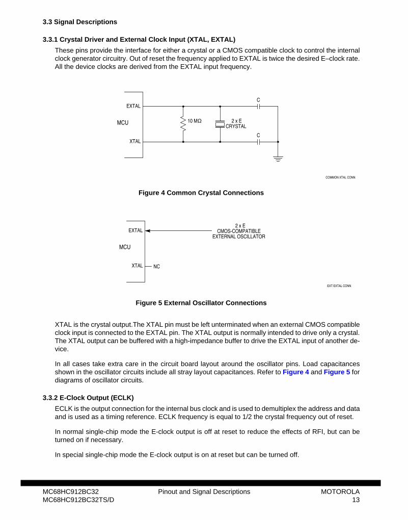
3.3.1 Crystal Driver and External Clock Input (XTAL, EXTAL)
These pins provide the interface for either a crystal or a CMOS compatible clock to control the internalclock generator circuitry. Out of reset the frequency applied to EXTAL is twice the desired E–clock rate.All the device clocks are derived from the EXTAL input frequency.
Figure 4 Common Crystal Connections
Figure 5 External Oscillator Connections
XTAL is the crystal output.The XTAL pin must be left unterminated when an external CMOS compatibleclock input is connected to the EXTAL pin. The XTAL output is normally intended to drive only a crystal.The XTAL output can be buffered with a high-impedance buffer to drive the EXTAL input of another de-vice.
In all cases take extra care in the circuit board layout around the oscillator pins. Load capacitancesshown in the oscillator circuits include all stray layout capacitances. Refer to Figure 4 and Figure 5 fordiagrams of oscillator circuits.
3.3.2 E-Clock Output (ECLK)
ECLK is the output connection for the internal bus clock and is used to demultiplex the address and dataand is used as a timing reference. ECLK frequency is equal to 1/2 the crystal frequency out of reset.
In normal single-chip mode the E-clock output is off at reset to reduce the effects of RFI, but can beturned on if necessary.
In special single-chip mode the E-clock output is on at reset but can be turned off.
10 MΩMCU
C
C
EXTAL
XTAL
2 x ECRYSTAL
COMMON XTAL CONN
NC
MCU
EXTAL
XTAL
2 x ECMOS-COMPATIBLE
EXT EXTAL CONN
EXTERNAL OSCILLATOR
MC68HC912BC32 Pinout and Signal Descriptions MOTOROLAMC68HC912BC32TS/D 13
In special peripheral mode the E clock is an input to the MCU.
All clocks, including the E clock, are halted when the MCU is in STOP mode. It is possible to configurethe MCU to interface to slow external memory. ECLK can be stretched for such accesses.
3.3.3 Reset (RESET)
An active low bidirectional control signal, RESET, acts as an input to initialize the MCU to a known start-up state. It also acts as an open-drain output to indicate that an internal failure has been detected ineither the clock monitor or COP watchdog circuit. The MCU goes into reset asynchronously and comesout of reset synchronously. This allows the part to reach a proper reset state even if the clocks havefailed, while allowing synchronized operation when starting out of reset.
It is possible to determine whether a reset was caused by an internal source or an external source. Aninternal source drives the pin low for 16 cycles; eight cycles later the pin is sampled. If the pin has re-turned high, either the COP watchdog vector or clock monitor vector will be taken. If the pin is still low,the external reset is determined to be active and the reset vector is taken. Hold reset low for at least 32cycles to assure that the reset vector is taken in the event that an internal COP watchdog time-out orclock monitor fail occurs.
3.3.4 Maskable Interrupt Request (IRQ)
The IRQ input provides a means of applying asynchronous interrupt requests to the MCU. Either fallingedge-sensitive triggering or level-sensitive triggering is program selectable (INTCR register). IRQ is al-ways configured to level-sensitive triggering at reset. When the MCU is reset the IRQ function ismasked in the condition code register.
This pin is always an input and can always be read. In special modes it can be used to apply externalEEPROM VPP in support of EEPROM testing. External VPP is not needed for normal EEPROM programand erase cycles. Because the IRQ pin is also used as an EEPROM programming voltage pin, there isan internal resistive pull-up on the pin.
3.3.5 Nonmaskable Interrupt (XIRQ)
The XIRQ input provides a means of requesting a nonmaskable interrupt after reset initialization. Duringreset, the X bit in the condition code register (CCR) is set and any interrupt is masked until MCU soft-ware enables it. Because the XIRQ input is level sensitive, it can be connected to a multiple-sourcewired-OR network. This pin is always an input and can always be read. There is an active pull-up onthis pin while in reset and immediately out of reset. The pullup can be turned off by clearing PUPE inthe PUCR register. XIRQ is often used as a power loss detect interrupt.
Whenever XIRQ or IRQ are used with multiple interrupt sources (IRQ must be configured for level-sen-sitive operation if there is more than one source of IRQ interrupt), each source must drive the interruptinput with an open-drain type of driver to avoid contention between outputs. There must also be an in-terlock mechanism at each interrupt source so that the source holds the interrupt line low until the MCUrecognizes and acknowledges the interrupt request. If the interrupt line is held low, the MCU will recog-nize another interrupt as soon as the interrupt mask bit in the MCU is cleared (normally upon return froman interrupt).
3.3.6 Mode Select (SMODN, MODA, and MODB)
The state of these pins during reset determine the MCU operating mode. After reset, MODA and MODBcan be configured as instruction queue tracking signals IPIPE0 and IPIPE1. MODA and MODB haveactive pulldowns during reset.
The SMODN pin can be used as BKGD or TAGHI after reset.
MOTOROLA Pinout and Signal Descriptions MC68HC912BC3214 MC68HC912BC32TS/D
3.3.7 Single-Wire Background Mode Pin (BKGD)
The BKGD pin receives and transmits serial background debugging commands. A special self-timingprotocol is used. The BKGD pin has an active pullup when configured as input; BKGD has no pullupcontrol. Refer to 16 Development Support.
3.3.8 External Address and Data Buses (ADDR[15:0] and DATA[15:0])
External bus pins share function with general-purpose I/O ports A and B. In single-chip operatingmodes, the pins can be used for I/O; in expanded modes, the pins are used for the external buses.
In expanded wide mode, ports A and B are used for multiplexed 16-bit data and address buses. PA[7:0]correspond to ADDR[15:8]/DATA[15:8]; PB[7:0] correspond to ADDR[7:0]/DATA[7:0].
In expanded narrow mode, ports A and B are used for the16-bit address bus, and an 8-bit data bus ismultiplexed with the most significant half of the address bus on port A. In this mode, 16-bit data is han-dled as two back-to-back bus cycles, one for the high byte followed by one for the low byte. PA[7:0]correspond to ADDR[15:8] and to DATA[15:8] or DATA[7:0], depending on the bus cycle. The state ofthe address pin should be latched at the rising edge of E. To allow for maximum address setup time atexternal devices, a transparent latch should be used.
3.3.9 Read/Write (R/W)
In all modes this pin can be used as I/O and is a general-purpose input with an active pull-up out ofreset. If the read/write function is required it should be enabled by setting the RDWE bit in the PEARregister. External writes will not be possible until enabled.
3.3.10 Low-Byte Strobe (LSTRB)
In all modes this pin can be used as I/O and is a general-purpose input with an active pull-up out ofreset. If the strobe function is required, it should be enabled by setting the LSTRE bit in the PEAR reg-ister. This signal is used in write operations and so external low byte writes will not be possible until thisfunction is enabled. This pin is also used as TAGLO in Special Expanded modes and is multiplexed withthe LSTRB function.
3.3.11 Instruction Queue Tracking Signals (IPIPE1 and IPIPE0)
These signals are used to track the state of the internal instruction execution queue. Execution state istime-multiplexed on the two signals. Refer to 16 Development Support.
3.3.12 Data Bus Enable (DBE)
The DBE pin (PE7) is an active low signal that will be asserted low during E-clock high time. DBE providesseparation between output of a multiplexed address and the input of data. When an external addressis stretched, DBE is asserted during what would be the last quarter cycle of the last E-clock cycle ofstretch. In expanded modes this pin is used to enable the drive control of external buses during externalreads. Use of the DBE is controlled by the NDBE bit in the PEAR register.DBE is enabled out of resetin expanded modes. This pin has an active pullup during and after reset in single chip modes.
MC68HC912BC32 Pinout and Signal Descriptions MOTOROLAMC68HC912BC32TS/D 15
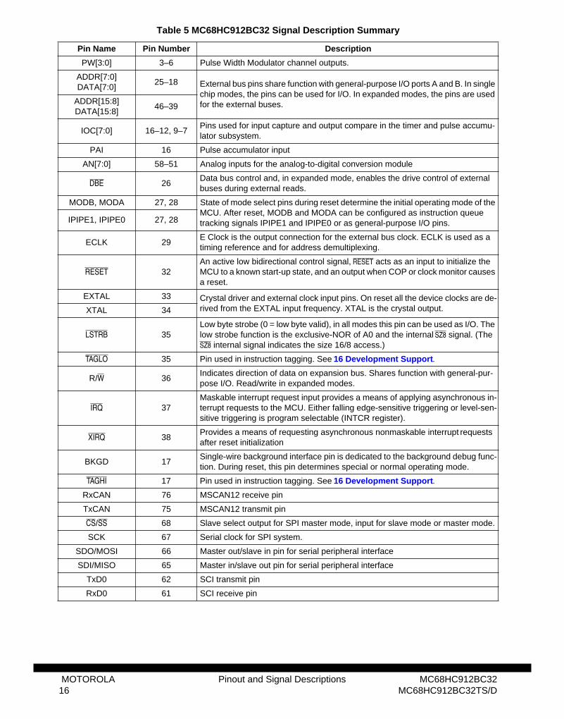
Table 5 MC68HC912BC32 Signal Description Summary
Pin Name Pin Number Description
PW[3:0] 3–6 Pulse Width Modulator channel outputs.
ADDR[7:0]DATA[7:0]
25–18 External bus pins share function with general-purpose I/O ports A and B. In single chip modes, the pins can be used for I/O. In expanded modes, the pins are used for the external buses.ADDR[15:8]
DATA[15:8]46–39
IOC[7:0] 16–12, 9–7 Pins used for input capture and output compare in the timer and pulse accumu-lator subsystem.
PAI 16 Pulse accumulator input
AN[7:0] 58–51 Analog inputs for the analog-to-digital conversion module
DBE 26Data bus control and, in expanded mode, enables the drive control of external buses during external reads.
MODB, MODA 27, 28 State of mode select pins during reset determine the initial operating mode of the MCU. After reset, MODB and MODA can be configured as instruction queue tracking signals IPIPE1 and IPIPE0 or as general-purpose I/O pins.IPIPE1, IPIPE0 27, 28
ECLK 29E Clock is the output connection for the external bus clock. ECLK is used as a timing reference and for address demultiplexing.
RESET 32An active low bidirectional control signal, RESET acts as an input to initialize the MCU to a known start-up state, and an output when COP or clock monitor causes a reset.
EXTAL 33 Crystal driver and external clock input pins. On reset all the device clocks are de-rived from the EXTAL input frequency. XTAL is the crystal output.XTAL 34
LSTRB 35Low byte strobe (0 = low byte valid), in all modes this pin can be used as I/O. The low strobe function is the exclusive-NOR of A0 and the internal SZ8 signal. (The SZ8 internal signal indicates the size 16/8 access.)
TAGLO 35 Pin used in instruction tagging. See 16 Development Support.
R/W 36Indicates direction of data on expansion bus. Shares function with general-pur-pose I/O. Read/write in expanded modes.
IRQ 37Maskable interrupt request input provides a means of applying asynchronous in-terrupt requests to the MCU. Either falling edge-sensitive triggering or level-sen-sitive triggering is program selectable (INTCR register).
XIRQ 38Provides a means of requesting asynchronous nonmaskable interrupt requests after reset initialization
BKGD 17Single-wire background interface pin is dedicated to the background debug func-tion. During reset, this pin determines special or normal operating mode.
TAGHI 17 Pin used in instruction tagging. See 16 Development Support.
RxCAN 76 MSCAN12 receive pin
TxCAN 75 MSCAN12 transmit pin
CS/SS 68 Slave select output for SPI master mode, input for slave mode or master mode.
SCK 67 Serial clock for SPI system.
SDO/MOSI 66 Master out/slave in pin for serial peripheral interface
SDI/MISO 65 Master in/slave out pin for serial peripheral interface
TxD0 62 SCI transmit pin
RxD0 61 SCI receive pin
MOTOROLA Pinout and Signal Descriptions MC68HC912BC3216 MC68HC912BC32TS/D
3.4 Port Signals
The MC68HC912BC32 incorporates eight ports which are used to control and access the various de-vice subsystems. When not used for these purposes, port pins may be used for general-purpose I/O.In addition to the pins described below, each port consists of a data register which can be read and writ-ten at any time, and, with the exception of port AD and PE[1:0], a data direction register which controlsthe direction of each pin. After reset all port pins are configured as input.
3.4.1 Port A
Port A pins are used for address and data in expanded modes. The port data register is not in the ad-dress map during expanded and peripheral mode operation. When it is in the map, port A can be reador written at anytime.
Register DDRA determines whether each port A pin is an input or output. DDRA is not in the addressmap during expanded and peripheral mode operation. Setting a bit in DDRA makes the correspondingbit in port A an output; clearing a bit in DDRA makes the corresponding bit in port A an input. The defaultreset state of DDRA is all zeroes.
When the PUPA bit in the PUCR register is set, all port A input pins are pulled-up internally by an activepull-up device. This bit has no effect if the port is being used in expanded modes as the pull-ups areinactive.
Setting the RDPA bit in register RDRIV causes all port A outputs to have reduced drive level. RDRIVcan be written once after reset. RDRIV is not in the address map in peripheral mode. Refer to 6 BusControl and Input/Output.
3.4.2 Port B
Port B pins are used for address and data in expanded modes. The port data register is not in the ad-dress map during expanded and peripheral mode operation. When it is in the map, port B can be reador written at anytime.
Register DDRB determines whether each port B pin is an input or output. DDRB is not in the addressmap during expanded and peripheral mode operation. Setting a bit in DDRB makes the correspondingbit in port B an output; clearing a bit in DDRB makes the corresponding bit in port B an input. The defaultreset state of DDRB is all zeroes.
When the PUPB bit in the PUCR register is set, all port B input pins are pulled-up internally by an activepull-up device. This bit has no effect if the port is being used in expanded modes as the pull-ups areinactive.
Setting the RDPB bit in register RDRIV causes all port B outputs to have reduced drive level. RDRIVcan be written once after reset. RDRIV is not in the address map in peripheral mode. Refer to 6 BusControl and Input/Output.
3.4.3 Port E
Port E pins operate differently from port A and B pins. Port E pins are used for bus control signals andinterrupt service request signals. When a pin is not used for one of these specific functions, it can beused as general-purpose I/O. However, two of the pins (PE[1:0]) can only be used for input, and thestates of these pins can be read in the port data register even when they are used for IRQ and XIRQ.
The PEAR register determines pin function, and register DDRE determines whether each pin is an inputor output when it is used for general-purpose I/O. PEAR settings override DDRE settings. BecausePE[1:0] are input-only pins, only DDRE[7:2] have effect. Setting a bit in the DDRE register makes thecorresponding bit in port E an output; clearing a bit in the DDRE register makes the corresponding bit
MC68HC912BC32 Pinout and Signal Descriptions MOTOROLAMC68HC912BC32TS/D 17
in port E an input. The default reset state of DDRE is all zeroes.
When the PUPE bit in the PUCR register is set, PE[7,3,2,0] are pulled up. PE[7,3,2,0] are pulled up ac-tive devices, while PE1 is always pulled up by means of an internal resistor.
Neither port E nor DDRE is in the map in peripheral mode; neither is in the internal map in expandedmodes with EME set.
Setting the RDPE bit in register RDRIV causes all port E outputs to have reduced drive level. RDRIVcan be written once after reset. RDRIV is not in the address map in peripheral mode. Refer to 6 BusControl and Input/Output.
3.4.4 Port CAN
The port CAN has five general-purpose I/O pins, PCAN[6:2]. The MSCAN12 receive pin, RxCAN, andtransmit pin, TxCAN, cannot be configured as general-purpose I/O on port CAN.
Register DDRCAN determines whether each port CAN pin PCAN[6:2] is an input or output. Setting abit in DDRCAN makes the corresponding pin in port CAN an output; clearing a bit makes the corre-sponding pin an input. After reset port CAN pins PCAN[6:2] are configured as inputs.
When a read to the port CAN is performed, the value read for the MSB depends on the MSB, PCAN7,of the port CAN data register, PORTCAN, and the MSB of DDRCAN: it is 0 if DDRCAN7=0 and isPCAN7 if DDRCAN7=1.
When the PUECAN bit in the PCTLCAN register is set, port CAN input pins PCAN[6:2] are pulled upinternally by an active pull-up device.
Setting the RDRCAN bit in register PCTLCAN causes the port CAN outputs PCAN[6:2] to have reduceddrive level. Levels are at normal drive capability after reset. RDRCAN can be written anytime after reset.Refer to 14 MSCAN12 Controller.
3.4.5 Port AD
Input to the analog-to-digital subsystem and general-purpose input. When analog-to-digital functionsare not enabled, the port has eight general-purpose input pins, PAD[7:0]. The ADPU bit in the ATDCTL2register enables the A/D function.
Port AD pins are inputs; no data direction register is associated with this port. The port has no resistiveinput loads and no reduced drive controls. Refer to 15 Analog-To-Digital Converter.
3.4.6 Port P
The four pulse-width modulation channel outputs share general-purpose port P pins. The PWM functionis enabled with the PWEN register. Enabling PWM pins takes precedence over the general-purposeport. When pulse-width modulation is not in use, the port pins may be used for general-purpose I/O.
Register DDRP determines pin direction of port P when used for general-purpose I/O. When DDRP bitsare set, the corresponding pin is configured for output. On reset the DDRP bits are cleared and the cor-responding pin is configured for input.
When the PUPP bit in the PWCTL register is set, all input pins are pulled up internally by an active pull-up device. Pullups are disabled after reset.
Setting the RDPP bit in the PWCTL register configures all port P outputs to have reduced drive levels.Levels are at normal drive capability after reset. The PWCTL register can be read or written anytimeafter reset. Refer to 11 Pulse Width Modulator.
MOTOROLA Pinout and Signal Descriptions MC68HC912BC3218 MC68HC912BC32TS/D
3.4.7 Port T
This port provides eight general-purpose I/O pins when not enabled for input capture and output com-pare in the timer and pulse accumulator subsystem. The TEN bit in the TSCR register enables the timerfunction. The pulse accumulator subsystem is enabled with the PAEN bit in the PACTL register.
Register DDRT determines pin direction of port T when used for general-purpose I/O. When DDRT bitsare set, the corresponding pin is configured for output. On reset the DDRT bits are cleared and the cor-responding pin is configured for input.
When the PUPT bit in the TMSK2 register is set, all input pins are pulled up internally by an active pull-up device. Pullups are disabled after reset.
Setting the RDPT bit in the TMSK2 register configures all port T outputs to have reduced drive levels.Levels are at normal drive capability after reset. The TMSK2 register can be read or written anytimeafter reset Refer to 12 Standard Timer Module.
3.4.8 Port S
Port S is the 8-bit interface to the standard serial interface consisting of the serial communications in-terface (SCI) and serial peripheral interface (SPI) subsystems. Port S pins are available for general-pur-pose parallel I/O when standard serial functions are not enabled.
Port S pins serve several functions depending on the various internal control registers. If WOMS bit inthe SC0CR1 register is set, the P-channel drivers of the output buffers are disabled for bits 0 through 1(2 through 3). If SWOM bit in the SP0CR1 register is set, the P-channel drivers of the output buffers aredisabled for bits 4 through 7. (wired-OR mode). The open drain control effects to both the serial and thegeneral-purpose outputs. If the RDPSx bits in the PURDS register are set, the appropriate Port S pindrive capabilities are reduced. If PUPSx bits in the PURDS register are set, the appropriate pull-up de-vice is connected to each port S pin which is programmed as a general-purpose input. If the pin is pro-grammed as a general-purpose output, the pull-up is disconnected from the pin regardless of the stateof the individual PUPSx bits. See 13 Serial Interface.
MC68HC912BC32 Pinout and Signal Descriptions MOTOROLAMC68HC912BC32TS/D 19
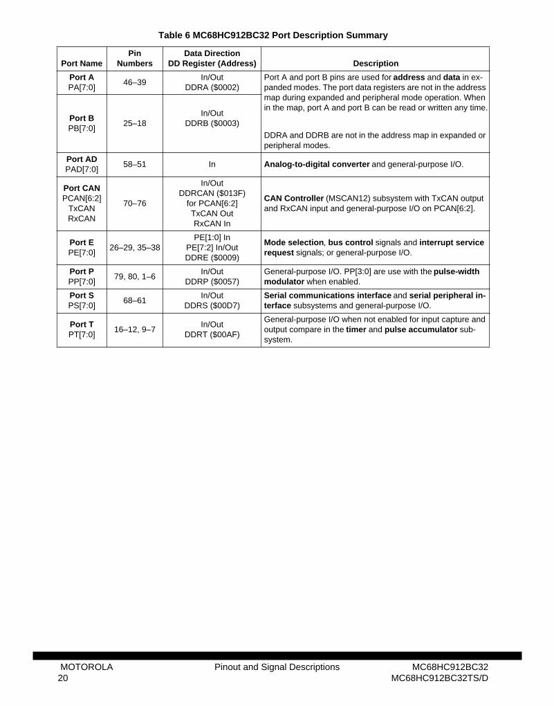
Table 6 MC68HC912BC32 Port Description Summary
Port NamePin
NumbersData Direction
DD Register (Address) Description
Port APA[7:0]
46–39In/Out
DDRA ($0002)Port A and port B pins are used for address and data in ex-panded modes. The port data registers are not in the address map during expanded and peripheral mode operation. When in the map, port A and port B can be read or written any time.
DDRA and DDRB are not in the address map in expanded or peripheral modes.
Port BPB[7:0]
25–18In/Out
DDRB ($0003)
Port ADPAD[7:0]
58–51 In Analog-to-digital converter and general-purpose I/O.
Port CAN PCAN[6:2]
TxCANRxCAN
70–76
In/OutDDRCAN ($013F)
for PCAN[6:2]TxCAN OutRxCAN In
CAN Controller (MSCAN12) subsystem with TxCAN output and RxCAN input and general-purpose I/O on PCAN[6:2].
Port EPE[7:0]
26–29, 35–38PE[1:0] In
PE[7:2] In/OutDDRE ($0009)
Mode selection, bus control signals and interrupt service request signals; or general-purpose I/O.
Port PPP[7:0]
79, 80, 1–6In/Out
DDRP ($0057)General-purpose I/O. PP[3:0] are use with the pulse-width modulator when enabled.
Port SPS[7:0]
68–61In/Out
DDRS ($00D7)Serial communications interface and serial peripheral in-terface subsystems and general-purpose I/O.
Port TPT[7:0]
16–12, 9–7In/Out
DDRT ($00AF)
General-purpose I/O when not enabled for input capture and output compare in the timer and pulse accumulator sub-system.
MOTOROLA Pinout and Signal Descriptions MC68HC912BC3220 MC68HC912BC32TS/D
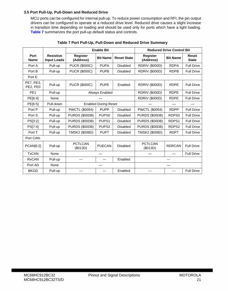
3.5 Port Pull-Up, Pull-Down and Reduced Drive
MCU ports can be configured for internal pull-up. To reduce power consumption and RFI, the pin outputdrivers can be configured to operate at a reduced drive level. Reduced drive causes a slight increasein transition time depending on loading and should be used only for ports which have a light loading.Table 7 summarizes the port pull-up default status and controls.
Table 7 Port Pull-Up, Pull-Down and Reduced Drive Summary
Enable Bit Reduced Drive Control Bit
PortName
ResistiveInput Loads
Register(Address)
Bit Name Reset StateRegister
(Address)Bit Name
Reset State
Port A Pull-up PUCR ($000C) PUPA Disabled RDRIV ($000D) RDPA Full Drive
Port B Pull-up PUCR ($000C) PUPB Disabled RDRIV ($000D) RDPB Full Drive
Port E:
PE7, PE3, PE2, PE0
Pull-up PUCR ($000C) PUPE Enabled RDRIV ($000D) RDPE Full Drive
PE1 Pull-up Always Enabled RDRIV ($000D) RDPE Full Drive
PE[6:4] None — RDRIV ($000D) RDPE Full Drive
PE[6:5] Pull-down Enabled During Reset — — —
Port P Pull-up PWCTL ($0054) PUPP Disabled PWCTL ($0054) RDPP Full Drive
Port S Pull-up PURDS ($00DB) PUPS0 Disabled PURDS ($00DB) RDPS0 Full Drive
PS[3:2] Pull-up PURDS ($00DB) PUPS1 Disabled PURDS ($00DB) RDPS1 Full Drive
PS[7:4] Pull-up PURDS ($00DB) PUPS2 Disabled PURDS ($00DB) RDPS2 Full Drive
Port T Pull-up TMSK2 ($008D) PUPT Disabled TMSK2 ($008D) RDPT Full Drive
Port CAN:
PCAN[6:2] Pull-upPCTLCAN ($013D)
PUECAN DisabledPCTLCAN ($013D)
RDRCAN Full Drive
TxCAN None — — — Full Drive
RxCAN Pull-up — — Enabled —
Port AD None — —
BKGD Pull-up — — Enabled — — Full Drive
MC68HC912BC32 Pinout and Signal Descriptions MOTOROLAMC68HC912BC32TS/D 21

MOTOROLA Pinout and Signal Descriptions MC68HC912BC3222 MC68HC912BC32TS/D
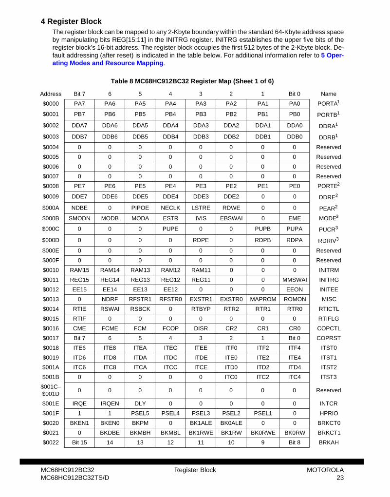
4 Register BlockThe register block can be mapped to any 2-Kbyte boundary within the standard 64-Kbyte address spaceby manipulating bits REG[15:11] in the INITRG register. INITRG establishes the upper five bits of theregister block’s 16-bit address. The register block occupies the first 512 bytes of the 2-Kbyte block. De-fault addressing (after reset) is indicated in the table below. For additional information refer to 5 Oper-ating Modes and Resource Mapping.
Table 8 MC68HC912BC32 Register Map (Sheet 1 of 6)
Address Bit 7 6 5 4 3 2 1 Bit 0 Name
$0000 PA7 PA6 PA5 PA4 PA3 PA2 PA1 PA0 PORTA1
$0001 PB7 PB6 PB5 PB4 PB3 PB2 PB1 PB0 PORTB1
$0002 DDA7 DDA6 DDA5 DDA4 DDA3 DDA2 DDA1 DDA0 DDRA1
$0003 DDB7 DDB6 DDB5 DDB4 DDB3 DDB2 DDB1 DDB0 DDRB1
$0004 0 0 0 0 0 0 0 0 Reserved
$0005 0 0 0 0 0 0 0 0 Reserved
$0006 0 0 0 0 0 0 0 0 Reserved
$0007 0 0 0 0 0 0 0 0 Reserved
$0008 PE7 PE6 PE5 PE4 PE3 PE2 PE1 PE0 PORTE2
$0009 DDE7 DDE6 DDE5 DDE4 DDE3 DDE2 0 0 DDRE2
$000A NDBE 0 PIPOE NECLK LSTRE RDWE 0 0 PEAR2
$000B SMODN MODB MODA ESTR IVIS EBSWAI 0 EME MODE3
$000C 0 0 0 PUPE 0 0 PUPB PUPA PUCR3
$000D 0 0 0 0 RDPE 0 RDPB RDPA RDRIV3
$000E 0 0 0 0 0 0 0 0 Reserved
$000F 0 0 0 0 0 0 0 0 Reserved
$0010 RAM15 RAM14 RAM13 RAM12 RAM11 0 0 0 INITRM
$0011 REG15 REG14 REG13 REG12 REG11 0 0 MMSWAI INITRG
$0012 EE15 EE14 EE13 EE12 0 0 0 EEON INITEE
$0013 0 NDRF RFSTR1 RFSTR0 EXSTR1 EXSTR0 MAPROM ROMON MISC
$0014 RTIE RSWAI RSBCK 0 RTBYP RTR2 RTR1 RTR0 RTICTL
$0015 RTIF 0 0 0 0 0 0 0 RTIFLG
$0016 CME FCME FCM FCOP DISR CR2 CR1 CR0 COPCTL
$0017 Bit 7 6 5 4 3 2 1 Bit 0 COPRST
$0018 ITE6 ITE8 ITEA ITEC ITEE ITF0 ITF2 ITF4 ITST0
$0019 ITD6 ITD8 ITDA ITDC ITDE ITE0 ITE2 ITE4 ITST1
$001A ITC6 ITC8 ITCA ITCC ITCE ITD0 ITD2 ITD4 ITST2
$001B 0 0 0 0 0 ITC0 ITC2 ITC4 ITST3
$001C–$001D
0 0 0 0 0 0 0 0 Reserved
$001E IRQE IRQEN DLY 0 0 0 0 0 INTCR
$001F 1 1 PSEL5 PSEL4 PSEL3 PSEL2 PSEL1 0 HPRIO
$0020 BKEN1 BKEN0 BKPM 0 BK1ALE BK0ALE 0 0 BRKCT0
$0021 0 BKDBE BKMBH BKMBL BK1RWE BK1RW BK0RWE BK0RW BRKCT1
MC68HC912BC32 Register Block MOTOROLAMC68HC912BC32TS/D 23
$0022 Bit 15 14 13 12 11 10 9 Bit 8 BRKAH
$0023 Bit 7 6 5 4 3 2 1 Bit 0 BRKAL
$0024 Bit 15 14 13 12 11 10 9 Bit 8 BRKDH
$0025 Bit 7 6 5 4 3 2 1 Bit 0 BRKDL
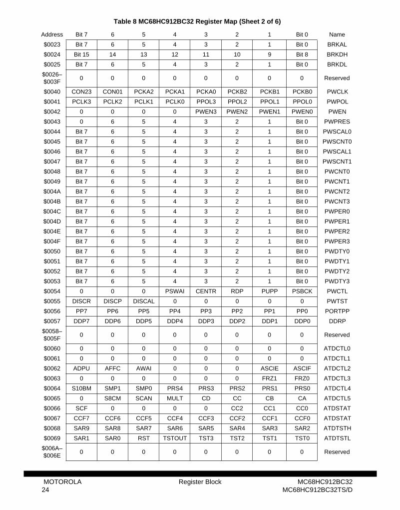
$0026–$003F
0 0 0 0 0 0 0 0 Reserved
$0040 CON23 CON01 PCKA2 PCKA1 PCKA0 PCKB2 PCKB1 PCKB0 PWCLK
$0041 PCLK3 PCLK2 PCLK1 PCLK0 PPOL3 PPOL2 PPOL1 PPOL0 PWPOL
$0042 0 0 0 0 PWEN3 PWEN2 PWEN1 PWEN0 PWEN
$0043 0 6 5 4 3 2 1 Bit 0 PWPRES
$0044 Bit 7 6 5 4 3 2 1 Bit 0 PWSCAL0
$0045 Bit 7 6 5 4 3 2 1 Bit 0 PWSCNT0
$0046 Bit 7 6 5 4 3 2 1 Bit 0 PWSCAL1
$0047 Bit 7 6 5 4 3 2 1 Bit 0 PWSCNT1
$0048 Bit 7 6 5 4 3 2 1 Bit 0 PWCNT0
$0049 Bit 7 6 5 4 3 2 1 Bit 0 PWCNT1
$004A Bit 7 6 5 4 3 2 1 Bit 0 PWCNT2
$004B Bit 7 6 5 4 3 2 1 Bit 0 PWCNT3
$004C Bit 7 6 5 4 3 2 1 Bit 0 PWPER0
$004D Bit 7 6 5 4 3 2 1 Bit 0 PWPER1
$004E Bit 7 6 5 4 3 2 1 Bit 0 PWPER2
$004F Bit 7 6 5 4 3 2 1 Bit 0 PWPER3
$0050 Bit 7 6 5 4 3 2 1 Bit 0 PWDTY0
$0051 Bit 7 6 5 4 3 2 1 Bit 0 PWDTY1
$0052 Bit 7 6 5 4 3 2 1 Bit 0 PWDTY2
$0053 Bit 7 6 5 4 3 2 1 Bit 0 PWDTY3
$0054 0 0 0 PSWAI CENTR RDP PUPP PSBCK PWCTL
$0055 DISCR DISCP DISCAL 0 0 0 0 0 PWTST
$0056 PP7 PP6 PP5 PP4 PP3 PP2 PP1 PP0 PORTPP
$0057 DDP7 DDP6 DDP5 DDP4 DDP3 DDP2 DDP1 DDP0 DDRP
$0058–$005F
0 0 0 0 0 0 0 0 Reserved
$0060 0 0 0 0 0 0 0 0 ATDCTL0
$0061 0 0 0 0 0 0 0 0 ATDCTL1
$0062 ADPU AFFC AWAI 0 0 0 ASCIE ASCIF ATDCTL2
$0063 0 0 0 0 0 0 FRZ1 FRZ0 ATDCTL3
$0064 S10BM SMP1 SMP0 PRS4 PRS3 PRS2 PRS1 PRS0 ATDCTL4
$0065 0 S8CM SCAN MULT CD CC CB CA ATDCTL5
$0066 SCF 0 0 0 0 CC2 CC1 CC0 ATDSTAT
$0067 CCF7 CCF6 CCF5 CCF4 CCF3 CCF2 CCF1 CCF0 ATDSTAT
$0068 SAR9 SAR8 SAR7 SAR6 SAR5 SAR4 SAR3 SAR2 ATDTSTH
$0069 SAR1 SAR0 RST TSTOUT TST3 TST2 TST1 TST0 ATDTSTL
$006A–
Table 8 MC68HC912BC32 Register Map (Sheet 2 of 6)
Address Bit 7 6 5 4 3 2 1 Bit 0 Name
MOTOROLA Register Block MC68HC912BC3224 MC68HC912BC32TS/D
$006E0 0 0 0 0 0 0 0 Reserved
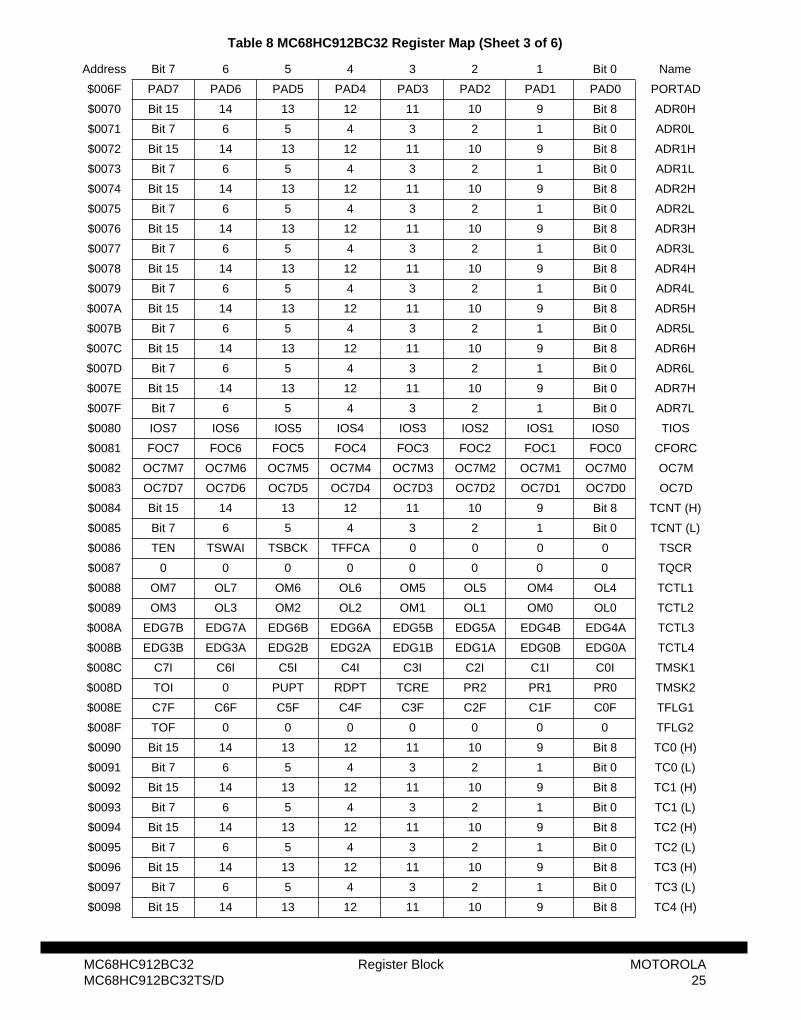
$006F PAD7 PAD6 PAD5 PAD4 PAD3 PAD2 PAD1 PAD0 PORTAD
$0070 Bit 15 14 13 12 11 10 9 Bit 8 ADR0H
$0071 Bit 7 6 5 4 3 2 1 Bit 0 ADR0L
$0072 Bit 15 14 13 12 11 10 9 Bit 8 ADR1H
$0073 Bit 7 6 5 4 3 2 1 Bit 0 ADR1L
$0074 Bit 15 14 13 12 11 10 9 Bit 8 ADR2H
$0075 Bit 7 6 5 4 3 2 1 Bit 0 ADR2L
$0076 Bit 15 14 13 12 11 10 9 Bit 8 ADR3H
$0077 Bit 7 6 5 4 3 2 1 Bit 0 ADR3L
$0078 Bit 15 14 13 12 11 10 9 Bit 8 ADR4H
$0079 Bit 7 6 5 4 3 2 1 Bit 0 ADR4L
$007A Bit 15 14 13 12 11 10 9 Bit 8 ADR5H
$007B Bit 7 6 5 4 3 2 1 Bit 0 ADR5L
$007C Bit 15 14 13 12 11 10 9 Bit 8 ADR6H
$007D Bit 7 6 5 4 3 2 1 Bit 0 ADR6L
$007E Bit 15 14 13 12 11 10 9 Bit 0 ADR7H
$007F Bit 7 6 5 4 3 2 1 Bit 0 ADR7L
$0080 IOS7 IOS6 IOS5 IOS4 IOS3 IOS2 IOS1 IOS0 TIOS
$0081 FOC7 FOC6 FOC5 FOC4 FOC3 FOC2 FOC1 FOC0 CFORC
$0082 OC7M7 OC7M6 OC7M5 OC7M4 OC7M3 OC7M2 OC7M1 OC7M0 OC7M
$0083 OC7D7 OC7D6 OC7D5 OC7D4 OC7D3 OC7D2 OC7D1 OC7D0 OC7D
$0084 Bit 15 14 13 12 11 10 9 Bit 8 TCNT (H)
$0085 Bit 7 6 5 4 3 2 1 Bit 0 TCNT (L)
$0086 TEN TSWAI TSBCK TFFCA 0 0 0 0 TSCR
$0087 0 0 0 0 0 0 0 0 TQCR
$0088 OM7 OL7 OM6 OL6 OM5 OL5 OM4 OL4 TCTL1
$0089 OM3 OL3 OM2 OL2 OM1 OL1 OM0 OL0 TCTL2
$008A EDG7B EDG7A EDG6B EDG6A EDG5B EDG5A EDG4B EDG4A TCTL3
$008B EDG3B EDG3A EDG2B EDG2A EDG1B EDG1A EDG0B EDG0A TCTL4
$008C C7I C6I C5I C4I C3I C2I C1I C0I TMSK1
$008D TOI 0 PUPT RDPT TCRE PR2 PR1 PR0 TMSK2
$008E C7F C6F C5F C4F C3F C2F C1F C0F TFLG1
$008F TOF 0 0 0 0 0 0 0 TFLG2
$0090 Bit 15 14 13 12 11 10 9 Bit 8 TC0 (H)
$0091 Bit 7 6 5 4 3 2 1 Bit 0 TC0 (L)
$0092 Bit 15 14 13 12 11 10 9 Bit 8 TC1 (H)
$0093 Bit 7 6 5 4 3 2 1 Bit 0 TC1 (L)
$0094 Bit 15 14 13 12 11 10 9 Bit 8 TC2 (H)
$0095 Bit 7 6 5 4 3 2 1 Bit 0 TC2 (L)
$0096 Bit 15 14 13 12 11 10 9 Bit 8 TC3 (H)
$0097 Bit 7 6 5 4 3 2 1 Bit 0 TC3 (L)
Table 8 MC68HC912BC32 Register Map (Sheet 3 of 6)
Address Bit 7 6 5 4 3 2 1 Bit 0 Name
MC68HC912BC32 Register Block MOTOROLAMC68HC912BC32TS/D 25
$0098 Bit 15 14 13 12 11 10 9 Bit 8 TC4 (H)
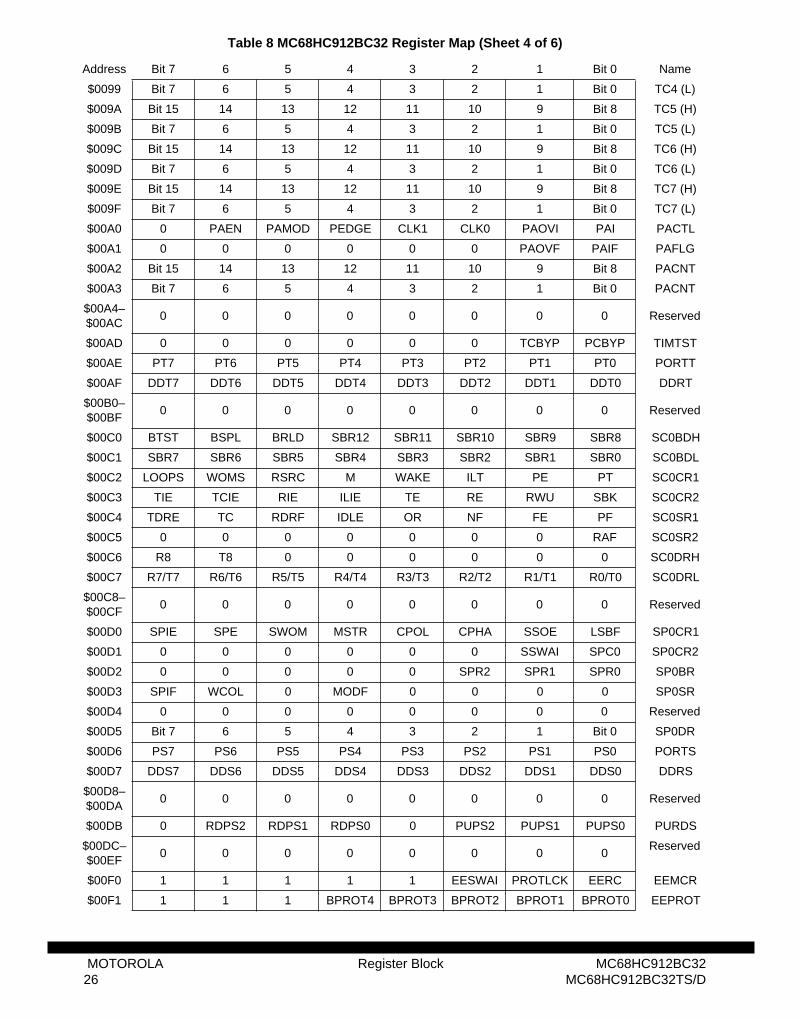
$0099 Bit 7 6 5 4 3 2 1 Bit 0 TC4 (L)
$009A Bit 15 14 13 12 11 10 9 Bit 8 TC5 (H)
$009B Bit 7 6 5 4 3 2 1 Bit 0 TC5 (L)
$009C Bit 15 14 13 12 11 10 9 Bit 8 TC6 (H)
$009D Bit 7 6 5 4 3 2 1 Bit 0 TC6 (L)
$009E Bit 15 14 13 12 11 10 9 Bit 8 TC7 (H)
$009F Bit 7 6 5 4 3 2 1 Bit 0 TC7 (L)
$00A0 0 PAEN PAMOD PEDGE CLK1 CLK0 PAOVI PAI PACTL
$00A1 0 0 0 0 0 0 PAOVF PAIF PAFLG
$00A2 Bit 15 14 13 12 11 10 9 Bit 8 PACNT
$00A3 Bit 7 6 5 4 3 2 1 Bit 0 PACNT
$00A4–$00AC
0 0 0 0 0 0 0 0 Reserved
$00AD 0 0 0 0 0 0 TCBYP PCBYP TIMTST
$00AE PT7 PT6 PT5 PT4 PT3 PT2 PT1 PT0 PORTT
$00AF DDT7 DDT6 DDT5 DDT4 DDT3 DDT2 DDT1 DDT0 DDRT
$00B0–$00BF
0 0 0 0 0 0 0 0 Reserved
$00C0 BTST BSPL BRLD SBR12 SBR11 SBR10 SBR9 SBR8 SC0BDH
$00C1 SBR7 SBR6 SBR5 SBR4 SBR3 SBR2 SBR1 SBR0 SC0BDL
$00C2 LOOPS WOMS RSRC M WAKE ILT PE PT SC0CR1
$00C3 TIE TCIE RIE ILIE TE RE RWU SBK SC0CR2
$00C4 TDRE TC RDRF IDLE OR NF FE PF SC0SR1
$00C5 0 0 0 0 0 0 0 RAF SC0SR2
$00C6 R8 T8 0 0 0 0 0 0 SC0DRH
$00C7 R7/T7 R6/T6 R5/T5 R4/T4 R3/T3 R2/T2 R1/T1 R0/T0 SC0DRL
$00C8–$00CF
0 0 0 0 0 0 0 0 Reserved
$00D0 SPIE SPE SWOM MSTR CPOL CPHA SSOE LSBF SP0CR1
$00D1 0 0 0 0 0 0 SSWAI SPC0 SP0CR2
$00D2 0 0 0 0 0 SPR2 SPR1 SPR0 SP0BR
$00D3 SPIF WCOL 0 MODF 0 0 0 0 SP0SR
$00D4 0 0 0 0 0 0 0 0 Reserved
$00D5 Bit 7 6 5 4 3 2 1 Bit 0 SP0DR
$00D6 PS7 PS6 PS5 PS4 PS3 PS2 PS1 PS0 PORTS
$00D7 DDS7 DDS6 DDS5 DDS4 DDS3 DDS2 DDS1 DDS0 DDRS
$00D8– $00DA
0 0 0 0 0 0 0 0 Reserved
$00DB 0 RDPS2 RDPS1 RDPS0 0 PUPS2 PUPS1 PUPS0 PURDS
$00DC– $00EF
0 0 0 0 0 0 0 0Reserved
$00F0 1 1 1 1 1 EESWAI PROTLCK EERC EEMCR
Table 8 MC68HC912BC32 Register Map (Sheet 4 of 6)
Address Bit 7 6 5 4 3 2 1 Bit 0 Name
MOTOROLA Register Block MC68HC912BC3226 MC68HC912BC32TS/D
$00F1 1 1 1 BPROT4 BPROT3 BPROT2 BPROT1 BPROT0 EEPROT
$00F2 EEODD EEVEN MARG EECPD EECPRD 0 EECPM 0 EETST
$00F3 BULKP 0 0 BYTE ROW ERASE EELAT EEPGM EEPROG
$00F4 0 0 0 0 0 0 0 LOCK FEELCK
$00F5 0 0 0 0 0 0 0 BOOTP FEEMCR
$00F6 FSTE GADR HVT FENLV FDISVFP VTCK STRE MWPR FEETST
$00F7 0 0 0 FEESWAI SVFP ERAS LAT ENPE FEECTL
$00F8-$00FF
- - - - - - - - Reserved
$0100 0 0 CSWAI SYNCH TLNKEN SLPAK SLPRQ SFTRES CMCR0
$0101 0 0 0 0 0 LOOPB WUPM CLKSRC CMCR1
$0102 SJW1 SJW0 BRP5 BRP4 BRP3 BRP2 BRP1 BRP0 CBTR0
$0103 SAMP TSEG22 TSEG21 TSEG20 TSEG13 TSEG12 TSEG11 TSEG10 CBTR1
$0104 WUPIF RWRNIF TWRNIF RERRIF TERRIF BOFFIF OVRIF RXF CRFLG
$0105 WUPIE RWRNIE TWRNIE RERRIE TERRIE BOFFIE OVRIE RXFIE CRIER
$0106 0 ABTAK2 ABTAK1 ABTAK0 0 TXE2 TXE1 TXE0 CTFLG
$0107 0 ABTRQ2 ABTRQ1 ABTRQ0 0 TXEIE2 TXEIE1 TXEIE0 CTCR
$0108 0 0 IDAM1 IDAM0 0 IDHIT2 IDHIT1 IDHIT0 CIDAC
$0109-$010D
- - - - - - - - Reserved
$010E RXERR7 RXERR6 RXERR5 RXERR4 RXERR3 RXERR2 RXERR1 RXERR0 CRXERR
$010F TXERR7 TXERR6 TXERR5 TXERR4 TXERR3 TXERR2 TXERR1 TXERR0 CTXERR
$0110 AC7 AC6 AC5 AC4 AC3 AC2 AC1 AC0 CIDAR0
$0111 AC7 AC6 AC5 AC4 AC3 AC2 AC1 AC0 CIDAR1
$0112 AC7 AC6 AC5 AC4 AC3 AC2 AC1 AC0 CIDAR2
$0113 AC7 AC6 AC5 AC4 AC3 AC2 AC1 AC0 CIDAR3
$0114 AM7 AM6 AM5 AM4 AM3 AM2 AM1 AM0 CIDMR0
$0115 AM7 AM6 AM5 AM4 AM3 AM2 AM1 AM0 CIDMR1
$0116 AM7 AM6 AM5 AM4 AM3 AM2 AM1 AM0 CIDMR2
$0117 AM7 AM6 AM5 AM4 AM3 AM2 AM1 AM0 CIDMR3
$0118 AC7 AC6 AC5 AC4 AC3 AC2 AC1 AC0 CIDAR4
$0119 AC7 AC6 AC5 AC4 AC3 AC2 AC1 AC0 CIDAR5
$011A AC7 AC6 AC5 AC4 AC3 AC2 AC1 AC0 CIDAR6
$011B AC7 AC6 AC5 AC4 AC3 AC2 AC1 AC0 CIDAR7
$011C AM7 AM6 AM5 AM4 AM3 AM2 AM1 AM0 CIDMR4
$011D AM7 AM6 AM5 AM4 AM3 AM2 AM1 AM0 CIDMR5
$011E AM7 AM6 AM5 AM4 AM3 AM2 AM1 AM0 CIDMR6
$011F AM7 AM6 AM5 AM4 AM3 AM2 AM1 AM0 CIDMR7
$0120-$013C
- - - - - - - - Reserved
$013D 0 0 0 0 0 0 PUECAN RDRCAN PCTLCAN
$013E PCAN7 PCAN6 PCAN5 PCAN4 PCAN3 PCAN2 TxCan RxCan PORTCAN
$013F DDRCAN7 DDRCAN6 DDRCAN5 DDRCAN4 DDRCAN3 DDRCAN2 0 0 DDRCAN
Table 8 MC68HC912BC32 Register Map (Sheet 5 of 6)
Address Bit 7 6 5 4 3 2 1 Bit 0 Name
MC68HC912BC32 Register Block MOTOROLAMC68HC912BC32TS/D 27
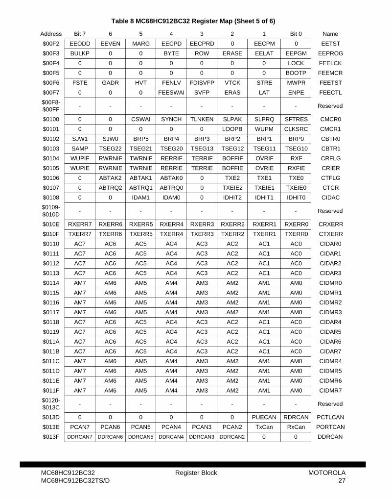
NOTES:1. Port A, port B, and data direction registers DDRA and DDRB are not in map in expanded and peripheral modes.2. Port E and DDRE not in map in peripheral mode; also not in map in expanded modes with EME set.3. Not in map in peripheral mode.4. u means, the register bit is undefined out of reset.
$0140-$014F u4 u u u u u u u
RECEIVE BUFFER
$0150-$015F
u u u u u u u uTRANSMIT BUFFER 0
$0160-$016F
u u u u u u u uTRANSMIT BUFFER 1
$0170-$017F
u u u u u u u uTRANSMIT BUFFER 2
Table 8 MC68HC912BC32 Register Map (Sheet 6 of 6)
Address Bit 7 6 5 4 3 2 1 Bit 0 Name
MOTOROLA Register Block MC68HC912BC3228 MC68HC912BC32TS/D
5 Operating Modes and Resource MappingEight possible operating modes determine the operating configuration of the MC68HC912BC32. Eachmode has an associated default memory map and external bus configuration. After reset, most systemresources can be mapped to other addresses by writing to the appropriate control registers.
5.1 Operating Modes
The operating mode out of reset is determined by the states of the BKGD, MODB, and MODA pins dur-ing reset.
The SMODN, MODB, and MODA bits in the MODE register show current operating mode and providelimited mode switching during operation. The states of the BKGD, MODB, and MODA pins are latchedinto these bits on the rising edge of the reset signal. During reset an active pullup is connected to theBKGD pin (as input) and active pulldowns are connected to the MODB and MODA pins. If an open oc-curs on any of these pins, the device will operate in normal single-chip mode.
There are two basic types of operating modes:
Normal modes — some registers and bits are protected against accidental changes.
Special modes — allow greater access to protected control registers and bits for special purposes suchas testing and emulation.
A system development and debug feature, background debug mode (BDM), is available in all modes.In special single-chip mode, BDM is active immediately after reset.
5.1.1 Normal Operating Modes
These modes provide three operating configurations. Background debugging is available in all threemodes, but must first be enabled for some operations by means of a BDM command. BDM can then bemade active by another BDM command.
Normal Expanded Wide Mode — This is a normal mode of operation in which the address and dataare multiplexed onto ports A and B. ADDR[15:8] and DATA[15:8] are present on port A. ADDR[7:0] andDATA[7:0] are present on port B.
Normal Expanded Narrow Mode — Port A is configured as the high byte of address multiplexed withthe 8-bit data bus. Port B is configured as the lower 8-bit address bus. This mode is used for lower costproduction systems that use 8-bit wide external EEPROMs or RAMs. Such systems take extra bus cy-cles to access 16-bit locations but this may be preferred over the extra cost of additional external mem-ory devices.
Table 9 Mode Selection
BKGD MODB MODA Mode Port A Port B
0 0 0 Special Single Chip General Purpose I/O General Purpose I/O
0 0 1 Special Expanded Narrow ADDR[15:8]/DATA[7:0] ADDR[7:0]
0 1 0 Special Peripheral ADDR/DATA ADDR/DATA
0 1 1 Special Expanded Wide ADDR/DATA ADDR/DATA
1 0 0 Normal Single Chip General Purpose I/O General Purpose I/O
1 0 1 Normal Expanded Narrow ADDR[15:8]/DATA[7:0] ADDR[7:0]
1 1 0 Reserved (Forced to Peripheral) — —
1 1 1 Normal Expanded Wide ADDR/DATA ADDR/DATA
MC68HC912BC32 Operating Modes and Resource Mapping MOTOROLAMC68HC912BC32TS/D 29
Normal Single-Chip Mode — There are no external address and data buses in this mode. All pins ofports A, B and E are configured as general-purpose I/O pins. Port E bits 1 and 0 are input-only withinternal pullups and the other 22 pins are bidirectional I/O pins that are initially configured as high-im-pedance inputs. Port E pullups are enabled upon reset; port A and B pullups are disabled upon reset.
5.1.2 Special Operating Modes
There are three special operating modes that correspond to normal operating modes. These operatingmodes are commonly used in factory testing and system development. In addition, there is a specialperipheral mode, in which an external master, such as an I.C. tester, can control the on-chip peripher-als.
Special Expanded Wide Mode — This mode can be used for emulation of normal expanded widemode and emulation of normal single-chip mode and 16-bit data bus. The bus control related pins inPORTE are all configured to serve their bus control output functions rather than general-purpose I/O.
Special Expanded Narrow Mode — This mode can be used for emulation of normal expanded narrowmode. In this mode external 16-bit data is handled as two back-to-back bus cycles, one for the high bytefollowed by one for the low byte. Internal operations continue to use full 16-bit data paths.
Special Single-Chip Mode — This mode can be used to force the MCU to active BDM mode to allowsystem debug through the BKGD pin. The MCU does not fetch the reset vector and execute applicationcode as it would in other modes. Instead, the active background mode is in control of CPU executionand BDM firmware is waiting for additional serial commands through the BKGD pin. There are no ex-ternal address and data buses in this mode. The MCU operates as a stand-alone device and all programand data space are on-chip. External port pins can be used for general-purpose I/O.
Special Peripheral Mode — The CPU is not active in this mode. An external master can control on-chip peripherals for testing purposes. It is not possible to change to or from this mode without goingthrough reset. Background debugging should not be used while the MCU is in special peripheral modeas internal bus conflicts between BDM and the external master can cause improper operation of bothmodes.
5.2 Background Debug Mode
Background debug mode (BDM) is an auxiliary operating mode that is used for system development.BDM is implemented in on-chip hardware and provides a full set of debug operations. Some BDM com-mands can be executed while the CPU is operating normally. Other BDM commands are firmwarebased, and require the BDM firmware to be enabled and active for execution.
In special single-chip mode, BDM is enabled and active immediately out of reset. BDM is available inall other operating modes, but must be enabled before it can be activated. BDM should not be used inspecial peripheral mode because of potential bus conflicts.
Once enabled, background mode can be made active by a serial command sent via the BKGD pin orexecution of a CPU12 BGND instruction. While background mode is active, the CPU can interpret spe-cial debugging commands, and read and write CPU registers, peripheral registers, and locations inmemory.
While BDM is active, the CPU executes code located in a small on-chip ROM mapped to addresses$FF00 to $FFFF; BDM control registers are accessible at addresses $FF00 to $FF06. The BDM ROMreplaces the regular system vectors while BDM is active. While BDM is active, the user memory from$FF00 to $FFFF is not in the map except through serial BDM commands.
BDM allows read and write access to internal memory-mapped registers and RAM, and read access toEEPROM and Flash EEPROM without interrupting the application code executing in the CPU. This non-
MOTOROLA Operating Modes and Resource Mapping MC68HC912BC3230 MC68HC912BC32TS/D
intrusive mode uses dead bus cycles to access the memory and in most cases will remain cycle deter-ministic. Refer to 16 Development Support for more details on BDM.
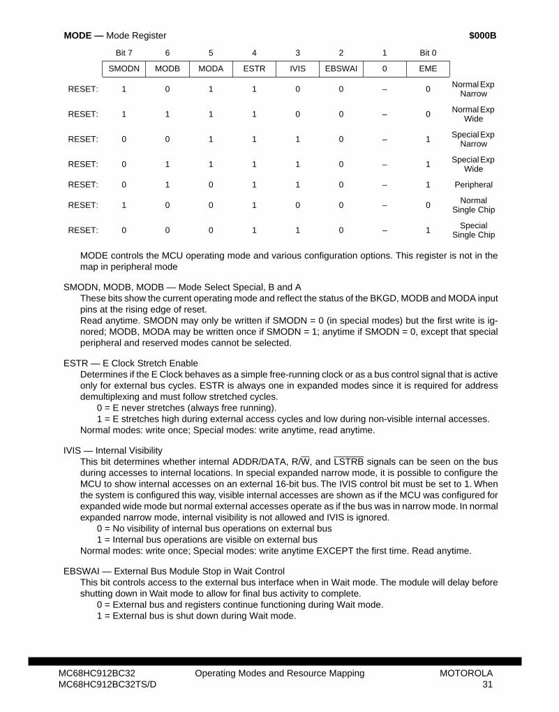
MODE controls the MCU operating mode and various configuration options. This register is not in themap in peripheral mode
SMODN, MODB, MODB — Mode Select Special, B and A These bits show the current operating mode and reflect the status of the BKGD, MODB and MODA inputpins at the rising edge of reset.Read anytime. SMODN may only be written if SMODN = 0 (in special modes) but the first write is ig-nored; MODB, MODA may be written once if SMODN = 1; anytime if SMODN = 0, except that specialperipheral and reserved modes cannot be selected.
ESTR — E Clock Stretch EnableDetermines if the E Clock behaves as a simple free-running clock or as a bus control signal that is activeonly for external bus cycles. ESTR is always one in expanded modes since it is required for addressdemultiplexing and must follow stretched cycles.
0 = E never stretches (always free running).1 = E stretches high during external access cycles and low during non-visible internal accesses.
Normal modes: write once; Special modes: write anytime, read anytime.
IVIS — Internal VisibilityThis bit determines whether internal ADDR/DATA, R/W, and LSTRB signals can be seen on the busduring accesses to internal locations. In special expanded narrow mode, it is possible to configure theMCU to show internal accesses on an external 16-bit bus. The IVIS control bit must be set to 1. Whenthe system is configured this way, visible internal accesses are shown as if the MCU was configured forexpanded wide mode but normal external accesses operate as if the bus was in narrow mode. In normalexpanded narrow mode, internal visibility is not allowed and IVIS is ignored.
0 = No visibility of internal bus operations on external bus1 = Internal bus operations are visible on external bus
Normal modes: write once; Special modes: write anytime EXCEPT the first time. Read anytime.
EBSWAI — External Bus Module Stop in Wait ControlThis bit controls access to the external bus interface when in Wait mode. The module will delay beforeshutting down in Wait mode to allow for final bus activity to complete.
0 = External bus and registers continue functioning during Wait mode.1 = External bus is shut down during Wait mode.
MODE — Mode Register $000B
Bit 7 6 5 4 3 2 1 Bit 0
SMODN MODB MODA ESTR IVIS EBSWAI 0 EME
RESET: 1 0 1 1 0 0 – 0 Normal Exp Narrow
RESET: 1 1 1 1 0 0 – 0 Normal Exp Wide
RESET: 0 0 1 1 1 0 – 1 Special Exp Narrow
RESET: 0 1 1 1 1 0 – 1 Special Exp Wide
RESET: 0 1 0 1 1 0 – 1 Peripheral
RESET: 1 0 0 1 0 0 – 0 NormalSingle Chip
RESET: 0 0 0 1 1 0 – 1 Special Single Chip
MC68HC912BC32 Operating Modes and Resource Mapping MOTOROLAMC68HC912BC32TS/D 31
EME — Emulate Port ERemoving the registers from the map allows the user to emulate the function of these registers exter-nally. In single-chip mode PORTE and DDRE are always in the map regardless of the state of this bit.
0 = PORTE and DDRE are in the memory map.1 = PORTE and DDRE are removed from the internal memory map (expanded mode).
Normal modes: write once; special modes: write anytime EXCEPT the first time. Read anytime.
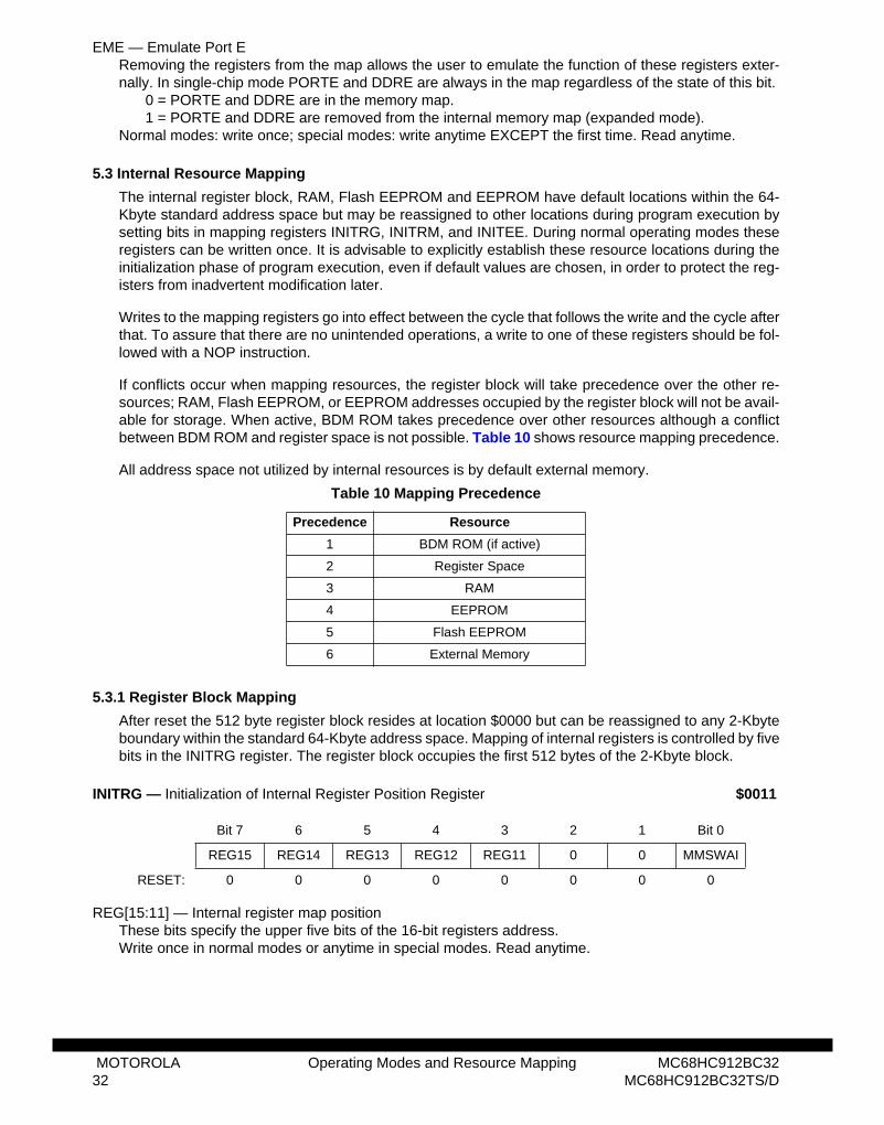
5.3 Internal Resource Mapping
The internal register block, RAM, Flash EEPROM and EEPROM have default locations within the 64-Kbyte standard address space but may be reassigned to other locations during program execution bysetting bits in mapping registers INITRG, INITRM, and INITEE. During normal operating modes theseregisters can be written once. It is advisable to explicitly establish these resource locations during theinitialization phase of program execution, even if default values are chosen, in order to protect the reg-isters from inadvertent modification later.
Writes to the mapping registers go into effect between the cycle that follows the write and the cycle afterthat. To assure that there are no unintended operations, a write to one of these registers should be fol-lowed with a NOP instruction.
If conflicts occur when mapping resources, the register block will take precedence over the other re-sources; RAM, Flash EEPROM, or EEPROM addresses occupied by the register block will not be avail-able for storage. When active, BDM ROM takes precedence over other resources although a conflictbetween BDM ROM and register space is not possible. Table 10 shows resource mapping precedence.
All address space not utilized by internal resources is by default external memory.
5.3.1 Register Block Mapping
After reset the 512 byte register block resides at location $0000 but can be reassigned to any 2-Kbyteboundary within the standard 64-Kbyte address space. Mapping of internal registers is controlled by fivebits in the INITRG register. The register block occupies the first 512 bytes of the 2-Kbyte block.
INITRG — Initialization of Internal Register Position Register $0011
REG[15:11] — Internal register map position These bits specify the upper five bits of the 16-bit registers address.Write once in normal modes or anytime in special modes. Read anytime.
Table 10 Mapping Precedence
Precedence Resource
1 BDM ROM (if active)
2 Register Space
3 RAM
4 EEPROM
5 Flash EEPROM
6 External Memory
Bit 7 6 5 4 3 2 1 Bit 0
REG15 REG14 REG13 REG12 REG11 0 0 MMSWAI
RESET: 0 0 0 0 0 0 0 0
MOTOROLA Operating Modes and Resource Mapping MC68HC912BC3232 MC68HC912BC32TS/D
MMSWAI — Memory Mapping Interface Stop in Wait ControlThis bit controls access to the memory mapping interface when in Wait mode.
0 = Memory mapping interface continues to function during Wait mode.1 = Memory mapping interface access is shut down during Wait mode.
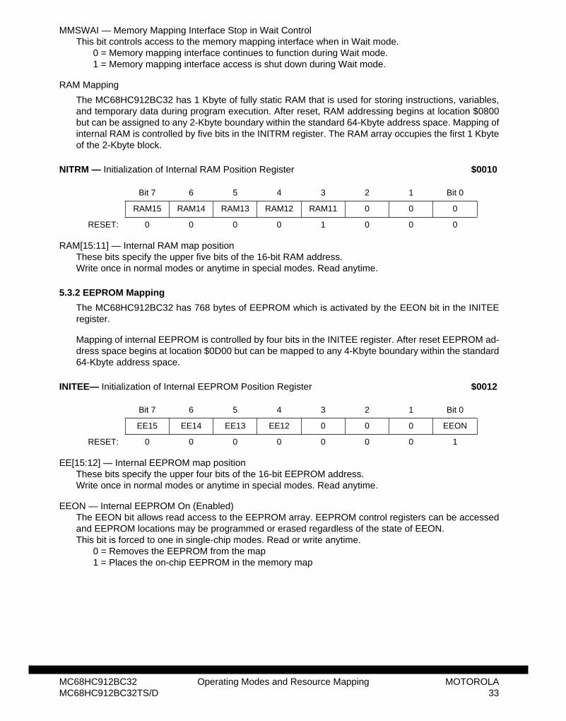
RAM Mapping
The MC68HC912BC32 has 1 Kbyte of fully static RAM that is used for storing instructions, variables,and temporary data during program execution. After reset, RAM addressing begins at location $0800but can be assigned to any 2-Kbyte boundary within the standard 64-Kbyte address space. Mapping ofinternal RAM is controlled by five bits in the INITRM register. The RAM array occupies the first 1 Kbyteof the 2-Kbyte block.
NITRM — Initialization of Internal RAM Position Register $0010
RAM[15:11] — Internal RAM map position These bits specify the upper five bits of the 16-bit RAM address.Write once in normal modes or anytime in special modes. Read anytime.
5.3.2 EEPROM Mapping
The MC68HC912BC32 has 768 bytes of EEPROM which is activated by the EEON bit in the INITEEregister.
Mapping of internal EEPROM is controlled by four bits in the INITEE register. After reset EEPROM ad-dress space begins at location $0D00 but can be mapped to any 4-Kbyte boundary within the standard64-Kbyte address space.
INITEE— Initialization of Internal EEPROM Position Register $0012
EE[15:12] — Internal EEPROM map position These bits specify the upper four bits of the 16-bit EEPROM address.Write once in normal modes or anytime in special modes. Read anytime.
EEON — Internal EEPROM On (Enabled)The EEON bit allows read access to the EEPROM array. EEPROM control registers can be accessedand EEPROM locations may be programmed or erased regardless of the state of EEON.This bit is forced to one in single-chip modes. Read or write anytime.
0 = Removes the EEPROM from the map1 = Places the on-chip EEPROM in the memory map
Bit 7 6 5 4 3 2 1 Bit 0
RAM15 RAM14 RAM13 RAM12 RAM11 0 0 0
RESET: 0 0 0 0 1 0 0 0
Bit 7 6 5 4 3 2 1 Bit 0
EE15 EE14 EE13 EE12 0 0 0 EEON
RESET: 0 0 0 0 0 0 0 1
MC68HC912BC32 Operating Modes and Resource Mapping MOTOROLAMC68HC912BC32TS/D 33
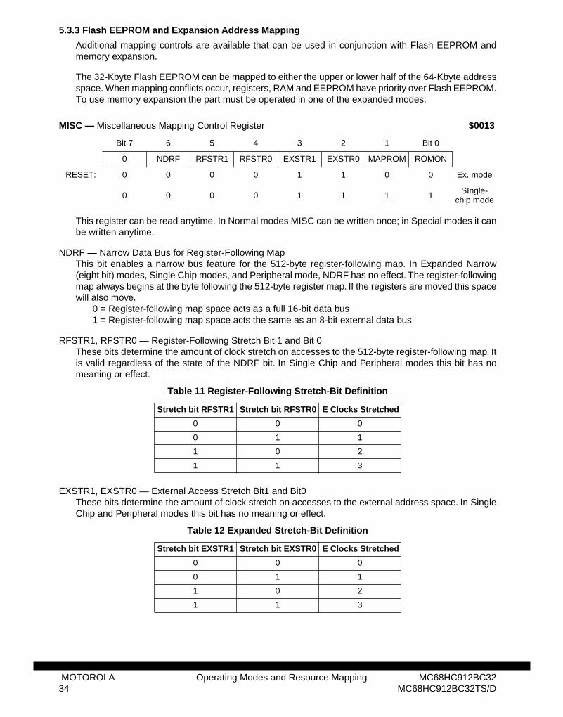
5.3.3 Flash EEPROM and Expansion Address Mapping
Additional mapping controls are available that can be used in conjunction with Flash EEPROM andmemory expansion.
The 32-Kbyte Flash EEPROM can be mapped to either the upper or lower half of the 64-Kbyte addressspace. When mapping conflicts occur, registers, RAM and EEPROM have priority over Flash EEPROM.To use memory expansion the part must be operated in one of the expanded modes.
This register can be read anytime. In Normal modes MISC can be written once; in Special modes it canbe written anytime.
NDRF — Narrow Data Bus for Register-Following MapThis bit enables a narrow bus feature for the 512-byte register-following map. In Expanded Narrow(eight bit) modes, Single Chip modes, and Peripheral mode, NDRF has no effect. The register-followingmap always begins at the byte following the 512-byte register map. If the registers are moved this spacewill also move.
0 = Register-following map space acts as a full 16-bit data bus1 = Register-following map space acts the same as an 8-bit external data bus
RFSTR1, RFSTR0 — Register-Following Stretch Bit 1 and Bit 0These bits determine the amount of clock stretch on accesses to the 512-byte register-following map. Itis valid regardless of the state of the NDRF bit. In Single Chip and Peripheral modes this bit has nomeaning or effect.
EXSTR1, EXSTR0 — External Access Stretch Bit1 and Bit0These bits determine the amount of clock stretch on accesses to the external address space. In SingleChip and Peripheral modes this bit has no meaning or effect.
MISC — Miscellaneous Mapping Control Register $0013
Bit 7 6 5 4 3 2 1 Bit 0
0 NDRF RFSTR1 RFSTR0 EXSTR1 EXSTR0 MAPROM ROMON
RESET: 0 0 0 0 1 1 0 0 Ex. mode
0 0 0 0 1 1 1 1 SIngle-chip mode
Table 11 Register-Following Stretch-Bit Definition
Stretch bit RFSTR1 Stretch bit RFSTR0 E Clocks Stretched
0 0 0
0 1 1
1 0 2
1 1 3
Table 12 Expanded Stretch-Bit Definition
Stretch bit EXSTR1 Stretch bit EXSTR0 E Clocks Stretched
0 0 0
0 1 1
1 0 2
1 1 3
MOTOROLA Operating Modes and Resource Mapping MC68HC912BC3234 MC68HC912BC32TS/D
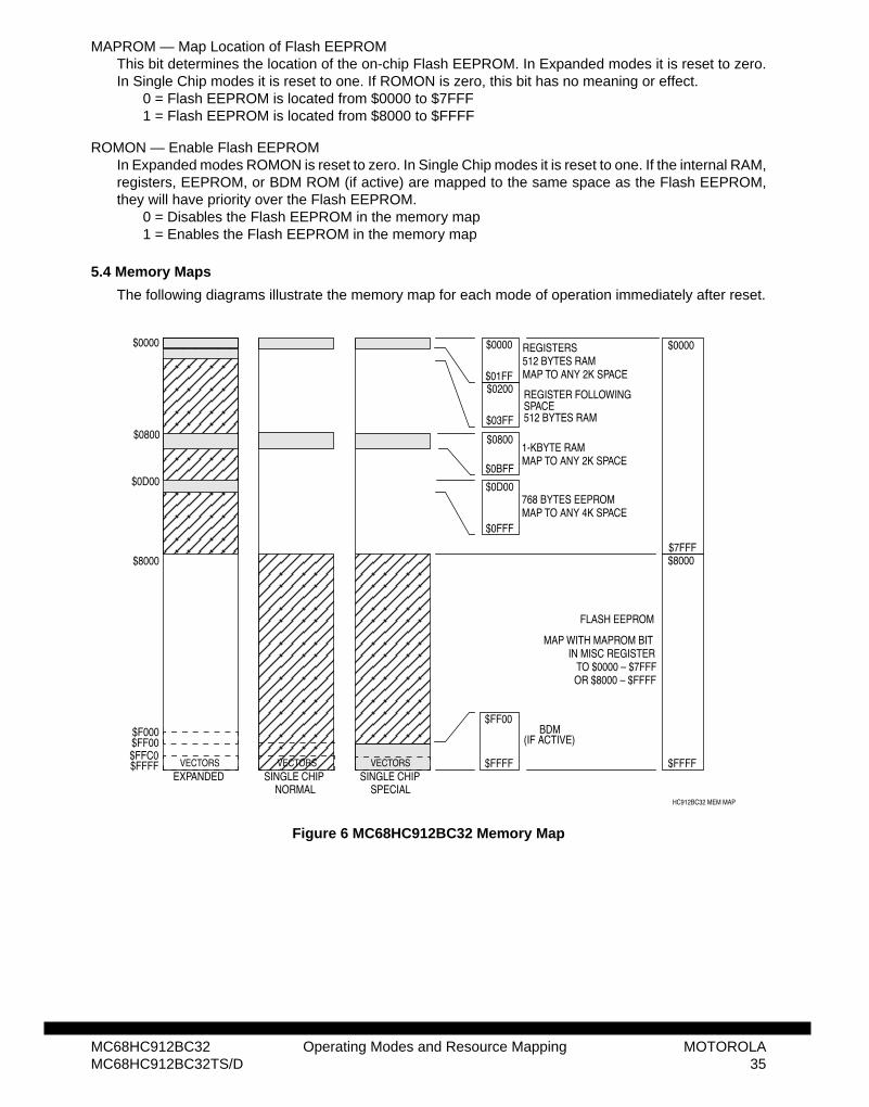
MAPROM — Map Location of Flash EEPROMThis bit determines the location of the on-chip Flash EEPROM. In Expanded modes it is reset to zero.In Single Chip modes it is reset to one. If ROMON is zero, this bit has no meaning or effect.
0 = Flash EEPROM is located from $0000 to $7FFF1 = Flash EEPROM is located from $8000 to $FFFF
ROMON — Enable Flash EEPROMIn Expanded modes ROMON is reset to zero. In Single Chip modes it is reset to one. If the internal RAM,registers, EEPROM, or BDM ROM (if active) are mapped to the same space as the Flash EEPROM,they will have priority over the Flash EEPROM.
0 = Disables the Flash EEPROM in the memory map1 = Enables the Flash EEPROM in the memory map
5.4 Memory Maps
The following diagrams illustrate the memory map for each mode of operation immediately after reset.
Figure 6 MC68HC912BC32 Memory Map
BDM(IF ACTIVE)
HC912BC32 MEM MAP
$8000
$FFFF$FFFF
FLASH EEPROM
$0000
$0800
$0D00
$0FFF
$FF00
$0000
$01FF
$0800
SINGLE CHIPSPECIAL
SINGLE CHIPNORMAL
EXPANDED
$8000
VECTORS VECTORS VECTORS
$FF00$F000
768 BYTES EEPROMMAP TO ANY 4K SPACE
1-KBYTE RAMMAP TO ANY 2K SPACE
REGISTERS
MAP TO ANY 2K SPACE
$FFFF$FFC0
$0BFF
MAP WITH MAPROM BIT
$0D00
512 BYTES RAM$0000
$7FFF
IN MISC REGISTERTO $0000 Ð $7FFFOR $8000 Ð $FFFF
$0200
$03FF
REGISTER FOLLOWINGSPACE512 BYTES RAM
MC68HC912BC32 Operating Modes and Resource Mapping MOTOROLAMC68HC912BC32TS/D 35

MOTOROLA Operating Modes and Resource Mapping MC68HC912BC3236 MC68HC912BC32TS/D
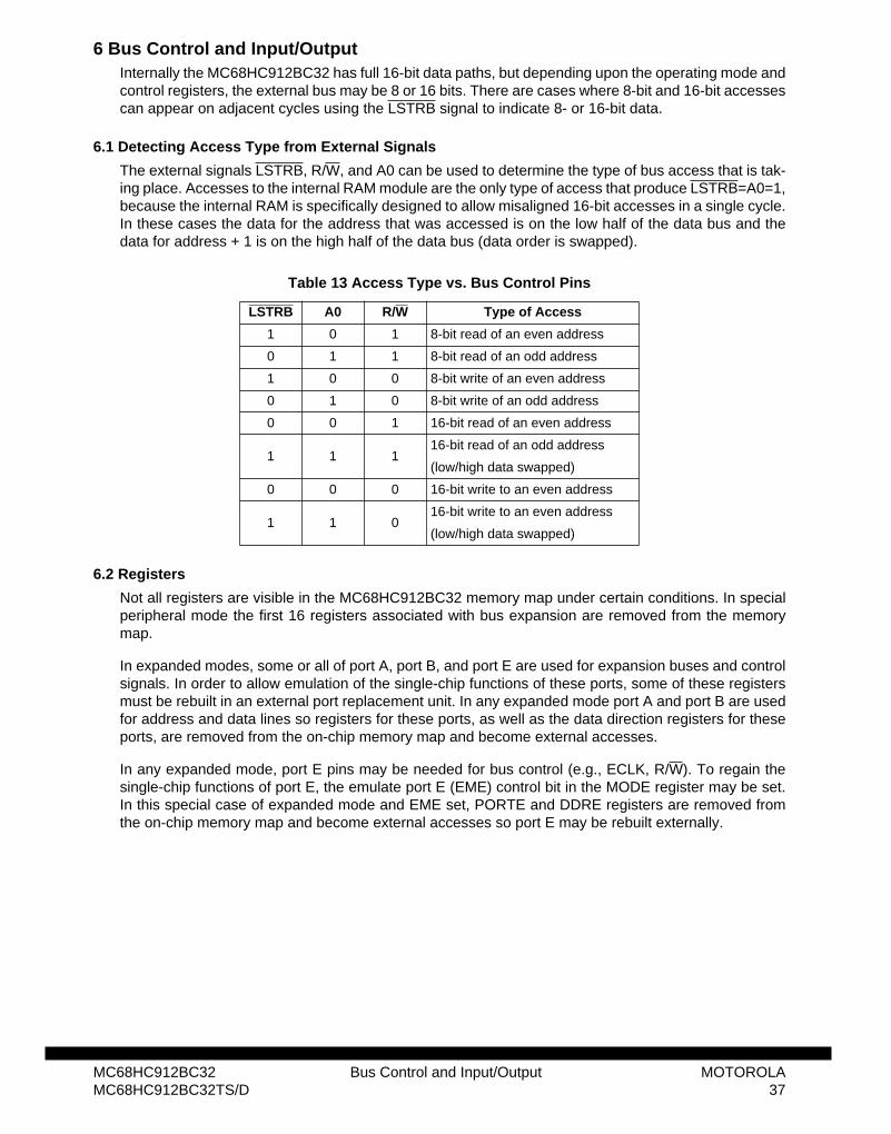
6 Bus Control and Input/OutputInternally the MC68HC912BC32 has full 16-bit data paths, but depending upon the operating mode andcontrol registers, the external bus may be 8 or 16 bits. There are cases where 8-bit and 16-bit accessescan appear on adjacent cycles using the LSTRB signal to indicate 8- or 16-bit data.
6.1 Detecting Access Type from External Signals
The external signals LSTRB, R/W, and A0 can be used to determine the type of bus access that is tak-ing place. Accesses to the internal RAM module are the only type of access that produce LSTRB=A0=1,because the internal RAM is specifically designed to allow misaligned 16-bit accesses in a single cycle.In these cases the data for the address that was accessed is on the low half of the data bus and thedata for address + 1 is on the high half of the data bus (data order is swapped).
6.2 Registers
Not all registers are visible in the MC68HC912BC32 memory map under certain conditions. In specialperipheral mode the first 16 registers associated with bus expansion are removed from the memorymap.
In expanded modes, some or all of port A, port B, and port E are used for expansion buses and controlsignals. In order to allow emulation of the single-chip functions of these ports, some of these registersmust be rebuilt in an external port replacement unit. In any expanded mode port A and port B are usedfor address and data lines so registers for these ports, as well as the data direction registers for theseports, are removed from the on-chip memory map and become external accesses.
In any expanded mode, port E pins may be needed for bus control (e.g., ECLK, R/W). To regain thesingle-chip functions of port E, the emulate port E (EME) control bit in the MODE register may be set.In this special case of expanded mode and EME set, PORTE and DDRE registers are removed fromthe on-chip memory map and become external accesses so port E may be rebuilt externally.
Table 13 Access Type vs. Bus Control Pins
LSTRB A0 R/W Type of Access
1 0 1 8-bit read of an even address
0 1 1 8-bit read of an odd address
1 0 0 8-bit write of an even address
0 1 0 8-bit write of an odd address
0 0 1 16-bit read of an even address
1 1 116-bit read of an odd address
(low/high data swapped)
0 0 0 16-bit write to an even address
1 1 016-bit write to an even address
(low/high data swapped)
MC68HC912BC32 Bus Control and Input/Output MOTOROLAMC68HC912BC32TS/D 37
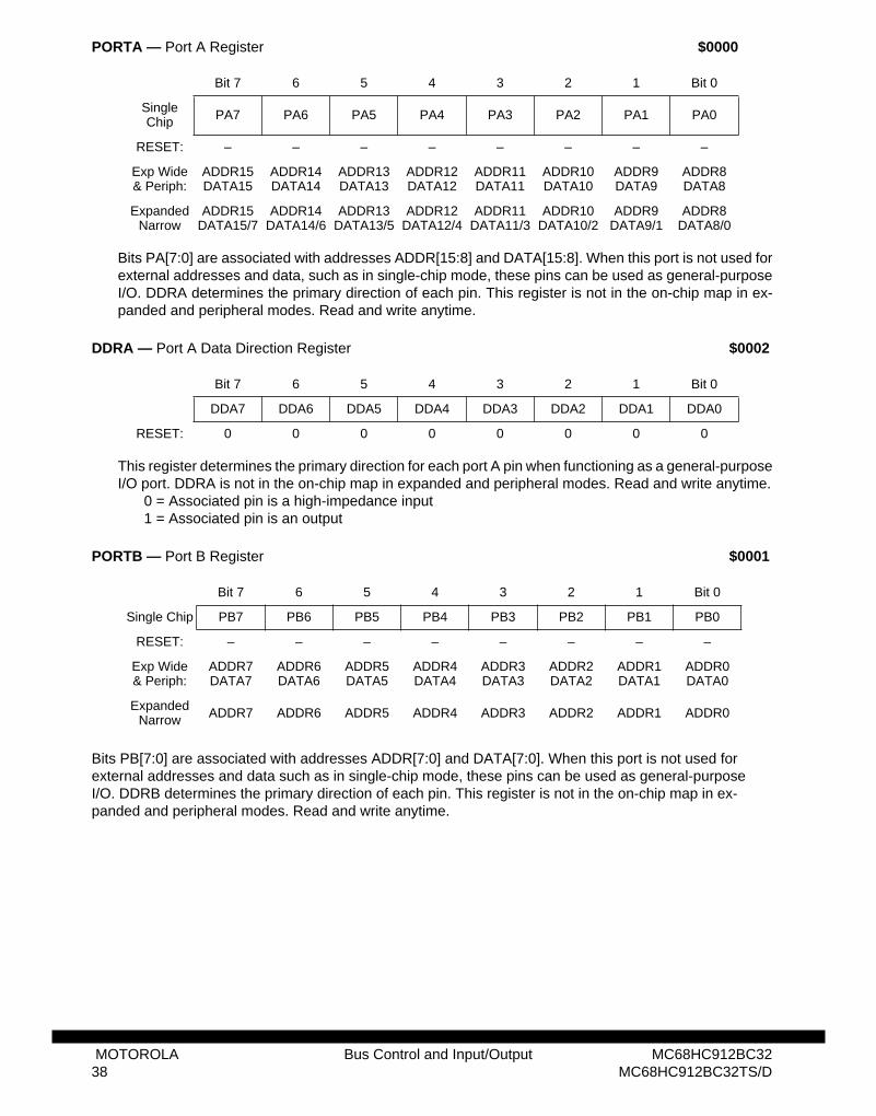
PORTA — Port A Register $0000
Bits PA[7:0] are associated with addresses ADDR[15:8] and DATA[15:8]. When this port is not used forexternal addresses and data, such as in single-chip mode, these pins can be used as general-purposeI/O. DDRA determines the primary direction of each pin. This register is not in the on-chip map in ex-panded and peripheral modes. Read and write anytime.
DDRA — Port A Data Direction Register $0002
This register determines the primary direction for each port A pin when functioning as a general-purposeI/O port. DDRA is not in the on-chip map in expanded and peripheral modes. Read and write anytime.
0 = Associated pin is a high-impedance input1 = Associated pin is an output
PORTB — Port B Register $0001
Bits PB[7:0] are associated with addresses ADDR[7:0] and DATA[7:0]. When this port is not used for external addresses and data such as in single-chip mode, these pins can be used as general-purpose I/O. DDRB determines the primary direction of each pin. This register is not in the on-chip map in ex-panded and peripheral modes. Read and write anytime.
Bit 7 6 5 4 3 2 1 Bit 0
Single Chip PA7 PA6 PA5 PA4 PA3 PA2 PA1 PA0
RESET: – – – – – – – –
Exp Wide& Periph:
ADDR15DATA15
ADDR14DATA14
ADDR13DATA13
ADDR12DATA12
ADDR11DATA11
ADDR10DATA10
ADDR9DATA9
ADDR8DATA8
Expanded Narrow
ADDR15DATA15/7
ADDR14DATA14/6
ADDR13DATA13/5
ADDR12DATA12/4
ADDR11DATA11/3
ADDR10DATA10/2
ADDR9DATA9/1
ADDR8DATA8/0
Bit 7 6 5 4 3 2 1 Bit 0
DDA7 DDA6 DDA5 DDA4 DDA3 DDA2 DDA1 DDA0
RESET: 0 0 0 0 0 0 0 0
Bit 7 6 5 4 3 2 1 Bit 0
Single Chip PB7 PB6 PB5 PB4 PB3 PB2 PB1 PB0
RESET: – – – – – – – –
Exp Wide& Periph:
ADDR7DATA7
ADDR6DATA6
ADDR5DATA5
ADDR4DATA4
ADDR3DATA3
ADDR2DATA2
ADDR1DATA1
ADDR0DATA0
Expanded Narrow ADDR7 ADDR6 ADDR5 ADDR4 ADDR3 ADDR2 ADDR1 ADDR0
MOTOROLA Bus Control and Input/Output MC68HC912BC3238 MC68HC912BC32TS/D
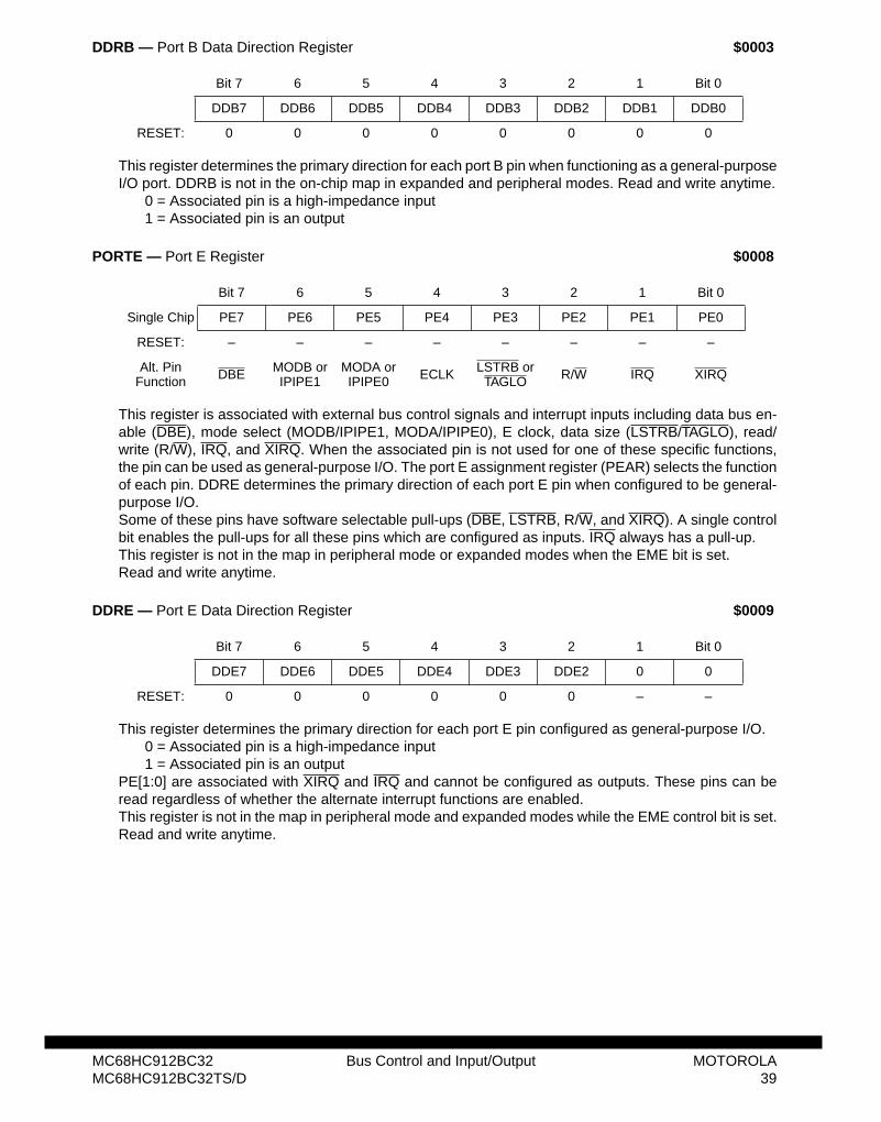
DDRB — Port B Data Direction Register $0003
This register determines the primary direction for each port B pin when functioning as a general-purposeI/O port. DDRB is not in the on-chip map in expanded and peripheral modes. Read and write anytime.
0 = Associated pin is a high-impedance input1 = Associated pin is an output
PORTE — Port E Register $0008
This register is associated with external bus control signals and interrupt inputs including data bus en-able (DBE), mode select (MODB/IPIPE1, MODA/IPIPE0), E clock, data size (LSTRB/TAGLO), read/write (R/W), IRQ, and XIRQ. When the associated pin is not used for one of these specific functions,the pin can be used as general-purpose I/O. The port E assignment register (PEAR) selects the functionof each pin. DDRE determines the primary direction of each port E pin when configured to be general-purpose I/O.Some of these pins have software selectable pull-ups (DBE, LSTRB, R/W, and XIRQ). A single controlbit enables the pull-ups for all these pins which are configured as inputs. IRQ always has a pull-up.This register is not in the map in peripheral mode or expanded modes when the EME bit is set.Read and write anytime.
DDRE — Port E Data Direction Register $0009
This register determines the primary direction for each port E pin configured as general-purpose I/O.0 = Associated pin is a high-impedance input1 = Associated pin is an output
PE[1:0] are associated with XIRQ and IRQ and cannot be configured as outputs. These pins can beread regardless of whether the alternate interrupt functions are enabled.This register is not in the map in peripheral mode and expanded modes while the EME control bit is set.Read and write anytime.
Bit 7 6 5 4 3 2 1 Bit 0
DDB7 DDB6 DDB5 DDB4 DDB3 DDB2 DDB1 DDB0
RESET: 0 0 0 0 0 0 0 0
Bit 7 6 5 4 3 2 1 Bit 0
Single Chip PE7 PE6 PE5 PE4 PE3 PE2 PE1 PE0
RESET: – – – – – – – –
Alt. Pin Function DBE MODB or
IPIPE1MODA or IPIPE0 ECLK LSTRB or
TAGLO R/W IRQ XIRQ
Bit 7 6 5 4 3 2 1 Bit 0
DDE7 DDE6 DDE5 DDE4 DDE3 DDE2 0 0
RESET: 0 0 0 0 0 0 – –
MC68HC912BC32 Bus Control and Input/Output MOTOROLAMC68HC912BC32TS/D 39
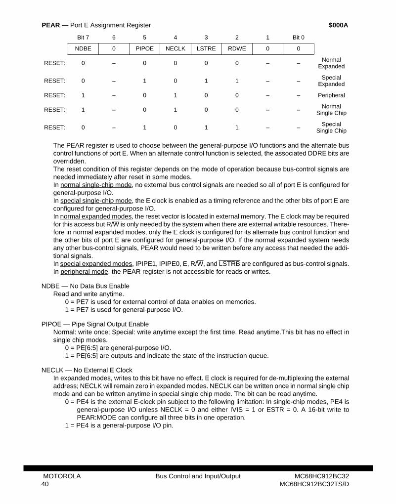
The PEAR register is used to choose between the general-purpose I/O functions and the alternate buscontrol functions of port E. When an alternate control function is selected, the associated DDRE bits areoverridden.The reset condition of this register depends on the mode of operation because bus-control signals areneeded immediately after reset in some modes. In normal single-chip mode, no external bus control signals are needed so all of port E is configured forgeneral-purpose I/O. In special single-chip mode, the E clock is enabled as a timing reference and the other bits of port E areconfigured for general-purpose I/O. In normal expanded modes, the reset vector is located in external memory. The E clock may be requiredfor this access but R/W is only needed by the system when there are external writable resources. There-fore in normal expanded modes, only the E clock is configured for its alternate bus control function andthe other bits of port E are configured for general-purpose I/O. If the normal expanded system needsany other bus-control signals, PEAR would need to be written before any access that needed the addi-tional signals. In special expanded modes, IPIPE1, IPIPE0, E, R/W, and LSTRB are configured as bus-control signals.In peripheral mode, the PEAR register is not accessible for reads or writes.
NDBE — No Data Bus EnableRead and write anytime.
0 = PE7 is used for external control of data enables on memories.1 = PE7 is used for general-purpose I/O.
PIPOE — Pipe Signal Output EnableNormal: write once; Special: write anytime except the first time. Read anytime.This bit has no effect insingle chip modes.
0 = PE[6:5] are general-purpose I/O.1 = PE[6:5] are outputs and indicate the state of the instruction queue.
NECLK — No External E ClockIn expanded modes, writes to this bit have no effect. E clock is required for de-multiplexing the externaladdress; NECLK will remain zero in expanded modes. NECLK can be written once in normal single chipmode and can be written anytime in special single chip mode. The bit can be read anytime.
0 = PE4 is the external E-clock pin subject to the following limitation: In single-chip modes, PE4 isgeneral-purpose I/O unless NECLK = 0 and either IVIS = 1 or ESTR = 0. A 16-bit write toPEAR:MODE can configure all three bits in one operation.
1 = PE4 is a general-purpose I/O pin.
PEAR — Port E Assignment Register $000A
Bit 7 6 5 4 3 2 1 Bit 0
NDBE 0 PIPOE NECLK LSTRE RDWE 0 0
RESET: 0 – 0 0 0 0 – – NormalExpanded
RESET: 0 – 1 0 1 1 – – SpecialExpanded
RESET: 1 – 0 1 0 0 – – Peripheral
RESET: 1 – 0 1 0 0 – – NormalSingle Chip
RESET: 0 – 1 0 1 1 – – SpecialSingle Chip
MOTOROLA Bus Control and Input/Output MC68HC912BC3240 MC68HC912BC32TS/D
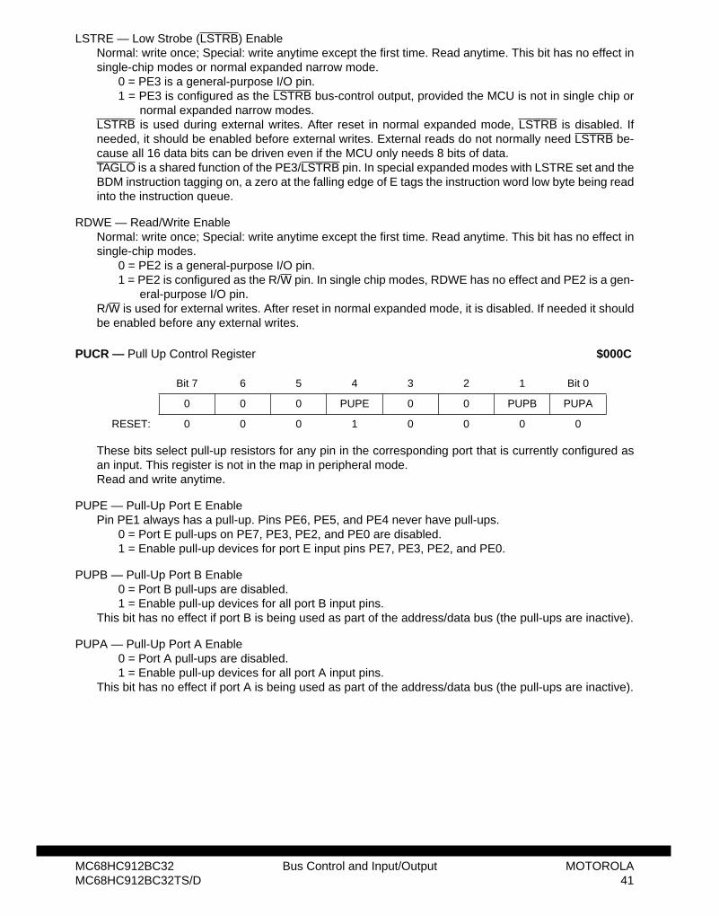
LSTRE — Low Strobe (LSTRB) EnableNormal: write once; Special: write anytime except the first time. Read anytime. This bit has no effect insingle-chip modes or normal expanded narrow mode.
0 = PE3 is a general-purpose I/O pin.1 = PE3 is configured as the LSTRB bus-control output, provided the MCU is not in single chip or
normal expanded narrow modes.LSTRB is used during external writes. After reset in normal expanded mode, LSTRB is disabled. Ifneeded, it should be enabled before external writes. External reads do not normally need LSTRB be-cause all 16 data bits can be driven even if the MCU only needs 8 bits of data.TAGLO is a shared function of the PE3/LSTRB pin. In special expanded modes with LSTRE set and theBDM instruction tagging on, a zero at the falling edge of E tags the instruction word low byte being readinto the instruction queue.
RDWE — Read/Write EnableNormal: write once; Special: write anytime except the first time. Read anytime. This bit has no effect insingle-chip modes.
0 = PE2 is a general-purpose I/O pin.1 = PE2 is configured as the R/W pin. In single chip modes, RDWE has no effect and PE2 is a gen-
eral-purpose I/O pin.R/W is used for external writes. After reset in normal expanded mode, it is disabled. If needed it shouldbe enabled before any external writes.
PUCR — Pull Up Control Register $000C
These bits select pull-up resistors for any pin in the corresponding port that is currently configured asan input. This register is not in the map in peripheral mode.Read and write anytime.
PUPE — Pull-Up Port E EnablePin PE1 always has a pull-up. Pins PE6, PE5, and PE4 never have pull-ups.
0 = Port E pull-ups on PE7, PE3, PE2, and PE0 are disabled.1 = Enable pull-up devices for port E input pins PE7, PE3, PE2, and PE0.
PUPB — Pull-Up Port B Enable0 = Port B pull-ups are disabled.1 = Enable pull-up devices for all port B input pins.
This bit has no effect if port B is being used as part of the address/data bus (the pull-ups are inactive).
PUPA — Pull-Up Port A Enable0 = Port A pull-ups are disabled.1 = Enable pull-up devices for all port A input pins.
This bit has no effect if port A is being used as part of the address/data bus (the pull-ups are inactive).
Bit 7 6 5 4 3 2 1 Bit 0
0 0 0 PUPE 0 0 PUPB PUPA
RESET: 0 0 0 1 0 0 0 0
MC68HC912BC32 Bus Control and Input/Output MOTOROLAMC68HC912BC32TS/D 41
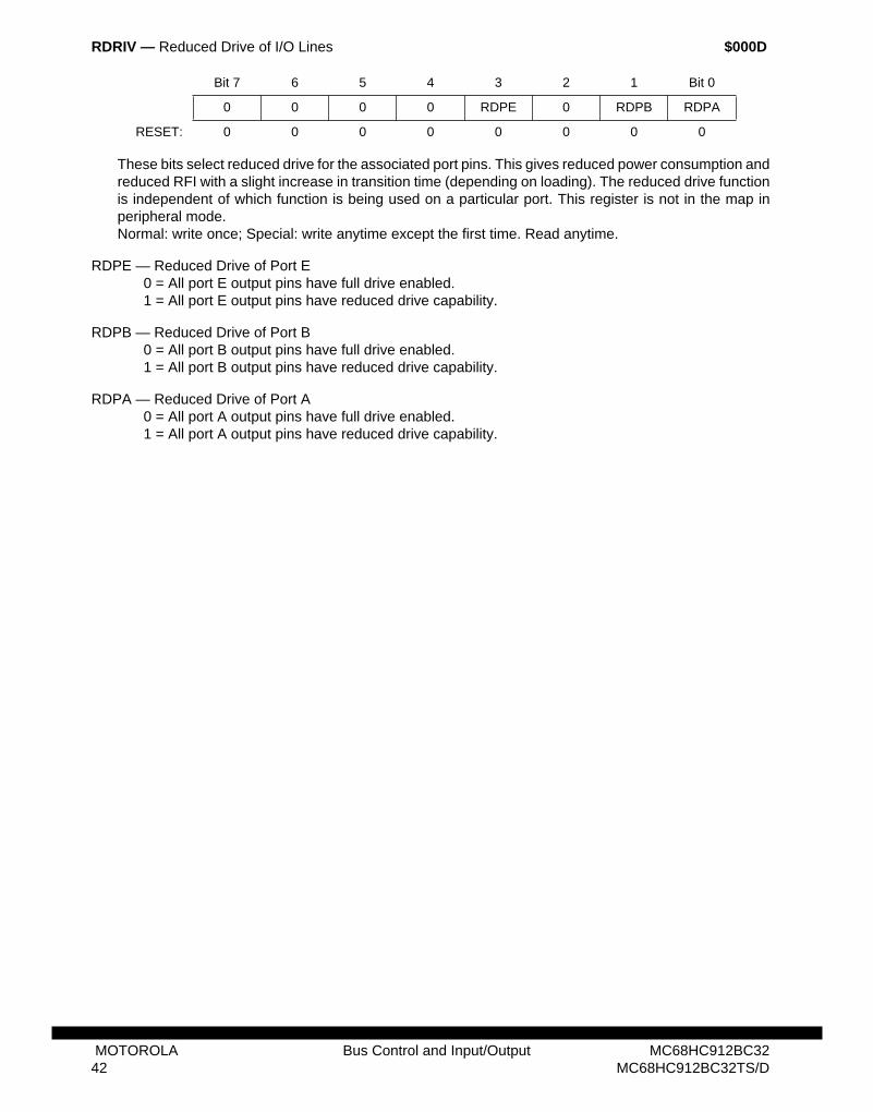
RDRIV — Reduced Drive of I/O Lines $000D
These bits select reduced drive for the associated port pins. This gives reduced power consumption andreduced RFI with a slight increase in transition time (depending on loading). The reduced drive functionis independent of which function is being used on a particular port. This register is not in the map inperipheral mode.Normal: write once; Special: write anytime except the first time. Read anytime.
RDPE — Reduced Drive of Port E0 = All port E output pins have full drive enabled.1 = All port E output pins have reduced drive capability.
RDPB — Reduced Drive of Port B0 = All port B output pins have full drive enabled.1 = All port B output pins have reduced drive capability.
RDPA — Reduced Drive of Port A0 = All port A output pins have full drive enabled.1 = All port A output pins have reduced drive capability.
Bit 7 6 5 4 3 2 1 Bit 0
0 0 0 0 RDPE 0 RDPB RDPA
RESET: 0 0 0 0 0 0 0 0
MOTOROLA Bus Control and Input/Output MC68HC912BC3242 MC68HC912BC32TS/D
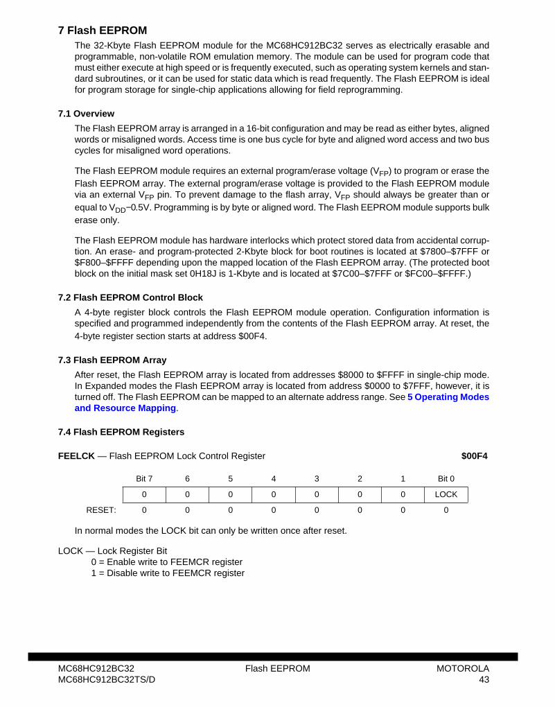
7 Flash EEPROMThe 32-Kbyte Flash EEPROM module for the MC68HC912BC32 serves as electrically erasable andprogrammable, non-volatile ROM emulation memory. The module can be used for program code thatmust either execute at high speed or is frequently executed, such as operating system kernels and stan-dard subroutines, or it can be used for static data which is read frequently. The Flash EEPROM is idealfor program storage for single-chip applications allowing for field reprogramming.
7.1 Overview
The Flash EEPROM array is arranged in a 16-bit configuration and may be read as either bytes, alignedwords or misaligned words. Access time is one bus cycle for byte and aligned word access and two buscycles for misaligned word operations.
The Flash EEPROM module requires an external program/erase voltage (VFP) to program or erase theFlash EEPROM array. The external program/erase voltage is provided to the Flash EEPROM modulevia an external VFP pin. To prevent damage to the flash array, VFP should always be greater than orequal to VDD−0.5V. Programming is by byte or aligned word. The Flash EEPROM module supports bulkerase only.
The Flash EEPROM module has hardware interlocks which protect stored data from accidental corrup-tion. An erase- and program-protected 2-Kbyte block for boot routines is located at $7800–$7FFF or$F800–$FFFF depending upon the mapped location of the Flash EEPROM array. (The protected bootblock on the initial mask set 0H18J is 1-Kbyte and is located at $7C00–$7FFF or $FC00–$FFFF.)
7.2 Flash EEPROM Control Block
A 4-byte register block controls the Flash EEPROM module operation. Configuration information isspecified and programmed independently from the contents of the Flash EEPROM array. At reset, the4-byte register section starts at address $00F4.
7.3 Flash EEPROM Array
After reset, the Flash EEPROM array is located from addresses $8000 to $FFFF in single-chip mode.In Expanded modes the Flash EEPROM array is located from address $0000 to $7FFF, however, it isturned off. The Flash EEPROM can be mapped to an alternate address range. See 5 Operating Modesand Resource Mapping.
7.4 Flash EEPROM Registers
FEELCK — Flash EEPROM Lock Control Register $00F4
In normal modes the LOCK bit can only be written once after reset.
LOCK — Lock Register Bit0 = Enable write to FEEMCR register1 = Disable write to FEEMCR register
Bit 7 6 5 4 3 2 1 Bit 0
0 0 0 0 0 0 0 LOCK
RESET: 0 0 0 0 0 0 0 0
MC68HC912BC32 Flash EEPROM MOTOROLAMC68HC912BC32TS/D 43
FEEMCR — Flash EEPROM Module Configuration Register $00F5
This register controls the operation of the Flash EEPROM array. BOOTP cannot be changed when theLOCK control bit in the FEELCK register is set or if ENPE in the FEECTL register is set.
BOOTP — Boot ProtectThe boot block is located at $7800–$7FFF or $F800–$FFFF depending upon the mapped location ofthe Flash EEPROM array and mask set ($7C00–$7FFF or $FC00–$FFFF for 1-Kbyte block).
0 = Enable erase and program of 1-Kbyte or 2-Kbyte boot block1 = Disable erase and program of 1-Kbyte or 2-Kbyte boot block
FEETST — Flash EEPROM Module Test Register $00F6
In normal mode, writes to FEETST control bits have no effect and always read zero. The FlashEEPROM module cannot be placed in test mode inadvertently during normal operation.
FSTE — Stress Test Enable0 = Disables the gate/drain stress circuitry1 = Enables the gate/drain stress circuitry
GADR — Gate/Drain Stress Test Select0 = Selects the drain stress circuitry1 = Selects the gate stress circuitry
HVT — Stress Test High Voltage Status0 = High voltage not present during stress test1 = High voltage present during stress test
FENLV — Enable Low Voltage0 = Disables low voltage transistor in current reference circuit1 = Enables low voltage transistor in current reference circuit
FDISVFP — Disable Status VFP Voltage LockWhen the VFP pin is below normal programming voltage the Flash module will not allow writing to theLAT bit; the user cannot erase or program the Flash module. The FDISVFP control bit enables writingto the LAT bit regardless of the voltage on the VFP pin.
0 = Enable the automatic lock mechanism if VFP is low1 = Disable the automatic lock mechanism if VFP is low
Bit 7 6 5 4 3 2 1 Bit 0
0 0 0 0 0 0 0 BOOTP
RESET: 0 0 0 0 0 0 0 1
Bit 7 6 5 4 3 2 1 Bit 0
FSTE GADR HVT FENLV FDISVFP VTCK STRE MWPR
RESET: 0 0 0 0 0 0 0 0
MOTOROLA Flash EEPROM MC68HC912BC3244 MC68HC912BC32TS/D
VTCK — VT Check Test EnableWhen VTCK is set, the Flash EEPROM module uses the VFP pin to control the control gate voltage; thesense amp time-out path is disabled. This allows for indirect measurements of the bit cells program anderase threshold. If VFP < VZBRK (breakdown voltage) the control gate will equal the VFP voltage. If VFP > VZBRK the control gate will be regulated by the following equation:
Vcontrol gate = VZBRK + 0.44 × (VFP − VZBRK)0 = VT test disable1 = VT test enable
STRE — Spare Test Row EnableThe spare test row consists of one Flash EEPROM array row. The reserved word at location 31 containsproduction test information which must be maintained through several erase cycles. When STRE is set,the decoding for the spare test row overrides the address lines which normally select the other rows inthe array.
0 = LIB accesses are to the Flash EEPROM array1 = Spare test row in array enabled if SMOD is active
MWPR — Multiple Word ProgrammingUsed primarily for testing, if MPWR = 1, the two least-significant address lines ADDR[1:0] will be ignoredwhen programming a Flash EEPROM location. The word location addressed if ADDR[1:0] = 00, alongwith the word location addressed if ADDR[1:0] = 10, will both be programmed with the same word datafrom the programming latches. This bit should not be changed during programming.
0 = Multiple word programming disabled1 = Program 32 bits of data
FEECTL — Flash EEPROM Control Register $00F7
This register controls the programming and erasure of the Flash EEPROM.
FEESWAI — Flash EEPROM Stop in Wait Control0 = Do not halt Flash EEPROM clock when the part is in wait mode.1 = Halt Flash EEPROM clock when the part is in wait mode.
NOTEThe FEESWAI bit cannot be asserted if the interrupt vector resides in the FlashEEPROM array.
SVFP — Status VFP VoltageSVFP is a read only bit.
0 = Voltage of VFP pin is below normal programming voltage levels1 = Voltage of VFP pin is above normal programming voltage levels
ERAS — Erase ControlThis bit can be read anytime or written when ENPE = 0. When set, all locations in the array will beerased at the same time. The boot block will be erased only if BOOTP = 0. This bit also affects the resultof attempted array reads. See Table 14 for more information. Status of ERAS cannot change if ENPEis set.
0 = Flash EEPROM configured for programming1 = Flash EEPROM configured for erasure
Bit 7 6 5 4 3 2 1 Bit 0
0 0 0 FEESWAI SVFP ERAS LAT ENPE
RESET: 0 0 0 0 0 0 0 0
MC68HC912BC32 Flash EEPROM MOTOROLAMC68HC912BC32TS/D 45
LAT — Latch ControlThis bit can be read anytime or written when ENPE = 0. When set, the Flash EEPROM is configuredfor programming or erasure and, upon the next valid write to the array, the address and data will belatched for the programming sequence. See Table 14 for the effects of LAT on array reads. A high volt-age detect circuit on the VFP pin will prevent assertion of the LAT bit when the programming voltage isat normal levels.
0 = Programming latches disabled1 = Programming latches enabled
ENPE — Enable Programming/Erase0 = Disables program/erase voltage to Flash EEPROM1 = Applies program/erase voltage to Flash EEPROM
ENPE can be asserted only after LAT has been asserted and a write to the data and address latcheshas occurred. If an attempt is made to assert ENPE when LAT is negated, or if the latches have notbeen written to after LAT was asserted, ENPE will remain negated after the write cycle is complete.The LAT, ERAS and BOOTP bits cannot be changed when ENPE is asserted. A write to FEECTL mayonly affect the state of ENPE. Attempts to read a Flash EEPROM array location in the Flash EEPROMmodule while ENPE is asserted will not return the data addressed. See Table 14 for more information.Flash EEPROM module control registers may be read or written while ENPE is asserted. If ENPE isasserted and LAT is negated on the same write access, no programming or erasure will be performed.
7.5 Operation
The Flash EEPROM can contain program and data. On reset, it can operate as a bootstrap memory toprovide the CPU with internal initialization information during the reset sequence.
7.5.1 Bootstrap Operation Single-Chip Mode
After reset, the CPU controlling the system will begin booting up by fetching the first program addressfrom address $FFFE.
7.5.2 Normal Operation
The Flash EEPROM allows a byte or aligned word read/write in one bus cycle. Misaligned word read/write require an additional bus cycle. The Flash EEPROM array responds to read operations only. Writeoperations are ignored.
7.5.3 Program/Erase Operation
An unprogrammed Flash EEPROM bit has a logic state of one. A bit must be programmed to changeits state from one to zero. Erasing a bit returns it to a logic one. The Flash EEPROM has a minimumprogram/erase life of 100 cycles. Programming or erasing the Flash EEPROM is accomplished by a se-ries of control register writes and a write to a set of programming latches.
Programming is restricted to a single byte or aligned word at a time as determined by internal signalSZ8 and ADDR[0]. The Flash EEPROM must first be completely erased prior to programming final datavalues. It is possible to program a location in the Flash EEPROM without erasing the entire array if thenew value does not require the changing of bit values from zero to one.
Table 14 Effects of ENPE, LAT and ERAS on Array Reads
ENPE LAT ERAS Result of Read
0 0 – Normal read of location addressed
0 1 0 Read of location being programmed
0 1 1 Normal read of location addressed
1 – – Read cycle is ignored
MOTOROLA Flash EEPROM MC68HC912BC3246 MC68HC912BC32TS/D

Read/Write Accesses During Program/Erase — During program or erase operations, read and writeaccesses may be different from those during normal operation and are affected by the state of the con-trol bits in the Flash EEPROM control register (FEECTL). The next write to any valid address to the ar-ray after LAT is set will cause the address and data to be latched into the programming latches. Oncethe address and data are latched, write accesses to the array will be ignored while LAT is set. Writes tothe control registers will occur normally.
Program/Erase Verification — When programming or erasing the Flash EEPROM array, a specialverification method is required to ensure that the program/erase process is reliable, and also to providethe longest possible life expectancy. This method requires stopping the program/erase sequence at pe-riods of tPPULSE (tEPULSE for erasing) to determine if the Flash EEPROM is programmed/erased. Afterthe location reaches the proper value, it must continue to be programmed/erased with additional marginpulses to ensure that it will remain programmed/erased. Failure to provide the margin pulses could leadto corrupted or unreliable data.
Program/Erase Sequence — To begin a program or erase sequence the external VFP voltage mustbe applied and stabilized. The ERAS bit must be set or cleared, depending on whether a program se-quence or an erase sequence is to occur. The LAT bit will be set to cause any subsequent data writtento a valid address within the Flash EEPROM to be latched into the programming address and data latch-es. The next Flash array write cycle must be either to the location that is to be programmed if a pro-gramming sequence is being performed, or, if erasing, to any valid Flash EEPROM array location.Writing the new address and data information to the Flash EEPROM is followed by assertion of ENPEto turn on the program/erase voltage to program/erase the new location(s). The LAT bit must be assert-ed and the address and data latched to allow the setting of the ENPE control bit. If the data and addresshave not been latched, an attempt to assert ENPE will be ignored and ENPE will remain negated afterthe write cycle to FEECTL is completed. The LAT bit must remain asserted and the ERAS bit must re-main in its current state as long as ENPE is asserted. A write to the LAT bit to clear it while ENPE is setwill be ignored. That is, after the write cycle, LAT will remain asserted. Likewise, an attempt to changethe state of ERAS will be ignored and the state of the ERAS bit will remain unchanged.
The programming software is responsible for all timing during a program sequence. This includes thetotal number of program pulses (nPP), the length of the program pulse (tPPULSE), the program marginpulses (pm) and the delay between turning off the high voltage and verifying the operation (tVPROG).
The erase software is responsible for all timing during an erase sequence. This includes the total num-ber of erase pulses (em), the length of the erase pulse (tEPULSE), the erase margin pulse or pulses, andthe delay between turning off the high voltage and verifying the operation (tVERASE).
Software also controls the supply of the proper program/erase voltage to the VFP pin, and should be atthe proper level before ENPE is set during a program/erase sequence.
A program/erase cycle should not be in progress when starting another program/erase, or while at-tempting to read from the array.
NOTEAlthough clearing ENPE disables the program/erase voltage (VFP) from the VFPpin to the array, care must be taken to ensure that VFP is at VDD whenever pro-gramming/erasing is not in progress. Not doing so could damage the part. Ensuringthat VFP is always greater or equal to VDD can be accomplished by controlling theVFP power supply with the programming software via an output pin. Alternatively,all programming and erasing can be done prior to installing the device on an appli-cation circuit board which can always connect VFP to VDD. Programming can alsobe accomplished by plugging the board into a special programming fixture which
MC68HC912BC32 Flash EEPROM MOTOROLAMC68HC912BC32TS/D 47
provides program/erase voltage to the VFP pin.
7.6 Programming the Flash EEPROM
Programming the Flash EEPROM is accomplished by the following sequence. The VFP pin voltagemust be at the proper level prior to executing step 4 the first time.
1. Apply program/erase voltage to the VFP pin.2. Clear ERAS and set the LAT bit in the FEECTL register to establish program mode and enable
programming address and data latches.3. Write data to a valid address. The address and data is latched. If BOOTP is asserted, an at-
tempt to program an address in the boot block will be ignored.4. Apply programming voltage by setting ENPE.5. Delay for one programming pulse (tPPULSE).6. Remove programming voltage by clearing ENPE.7. Delay while high voltage is turning off (tVPROG).8. Read the address location to verify that it has been programmed
• If the location is not programmed, repeat steps 4 through 7 until the location is programmedor until the specified maximum number of program pulses has been reached (nPP)
• If the location is programmed, repeat the same number of pulses as required to program thelocation. This provides 100% program margin.
9. Read the address location to verify that it remains programmed.10. Clear LAT.11. If there are more locations to program, repeat steps 2 through 10.12. Turn off VFP (reduce voltage on VFP pin to VDD).
The flowchart in Figure 7 demonstrates the recommended programming sequence.
MOTOROLA Flash EEPROM MC68HC912BC3248 MC68HC912BC32TS/D
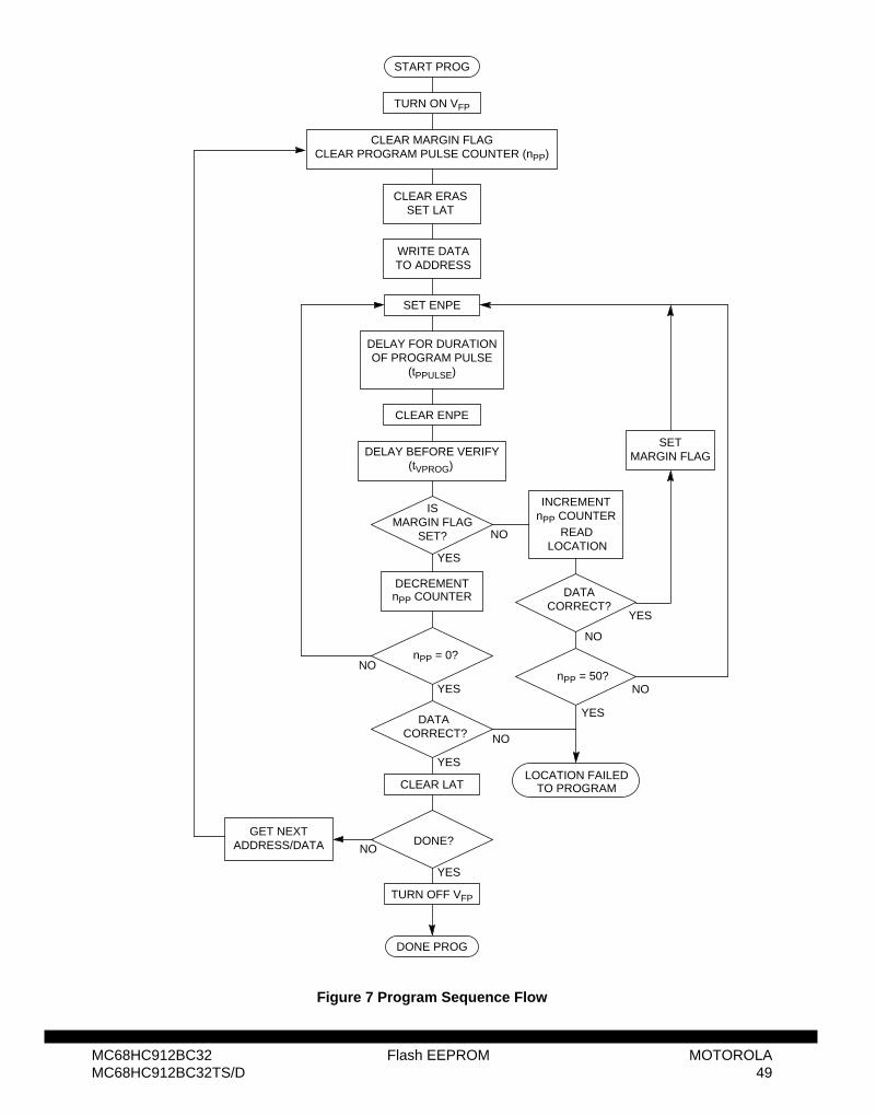
START PROG
SET LAT CLEAR ERAS
WRITE DATATO ADDRESS
SET ENPE
READ
GET NEXTADDRESS/DATA
NO
LOCATION FAILED
LOCATION
CLEAR MARGIN FLAG
INCREMENTnPP COUNTER
NO
DECREMENTnPP COUNTER
NO
YES
YES
YES
TO PROGRAM
TURN ON VFP
DELAY FOR DURATIONOF PROGRAM PULSE
(tPPULSE)
CLEAR ENPE
DELAY BEFORE VERIFY
ISMARGIN FLAG
SET? NO
YES
NO
YES
DATACORRECT?
SETMARGIN FLAG
DATACORRECT?
nPP = 0?
DONE?
TURN OFF VFP
(tVPROG)
nPP = 50?
YES
NO
DONE PROG
CLEAR PROGRAM PULSE COUNTER (nPP)
CLEAR LAT
MC68HC912BC32 Flash EEPROM MOTOROLAMC68HC912BC32TS/D 49
Figure 7 Program Sequence Flow
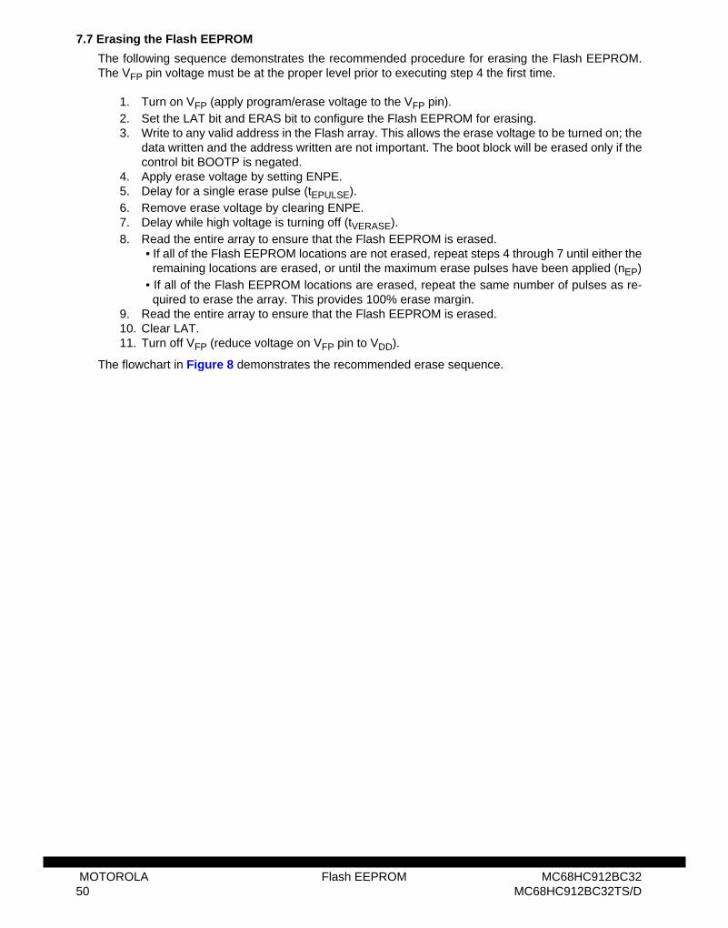
7.7 Erasing the Flash EEPROM
The following sequence demonstrates the recommended procedure for erasing the Flash EEPROM.The VFP pin voltage must be at the proper level prior to executing step 4 the first time.
1. Turn on VFP (apply program/erase voltage to the VFP pin).2. Set the LAT bit and ERAS bit to configure the Flash EEPROM for erasing.3. Write to any valid address in the Flash array. This allows the erase voltage to be turned on; the
data written and the address written are not important. The boot block will be erased only if thecontrol bit BOOTP is negated.
4. Apply erase voltage by setting ENPE. 5. Delay for a single erase pulse (tEPULSE). 6. Remove erase voltage by clearing ENPE. 7. Delay while high voltage is turning off (tVERASE). 8. Read the entire array to ensure that the Flash EEPROM is erased.
• If all of the Flash EEPROM locations are not erased, repeat steps 4 through 7 until either theremaining locations are erased, or until the maximum erase pulses have been applied (nEP)
• If all of the Flash EEPROM locations are erased, repeat the same number of pulses as re-quired to erase the array. This provides 100% erase margin.
9. Read the entire array to ensure that the Flash EEPROM is erased.10. Clear LAT.11. Turn off VFP (reduce voltage on VFP pin to VDD).
The flowchart in Figure 8 demonstrates the recommended erase sequence.
MOTOROLA Flash EEPROM MC68HC912BC3250 MC68HC912BC32TS/D
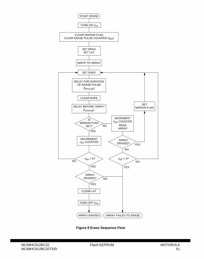
Figure 8 Erase Sequence Flow
START ERASE
SET LAT SET ERAS
WRITE TO ARRAY
SET ENPE
READ
NO
ARRAY FAILED TO ERASE
ARRAY
CLEAR MARGIN FLAG
INCREMENTnEP COUNTER
DECREMENTnEP COUNTER
NO
YES
YES
TURN ON VFP
DELAY FOR DURATIONOF ERASE PULSE
(tEPULSE)
CLEAR ENPE
DELAY BEFORE VERIFY
ISMARGIN FLAG
SET? NO
YES
NO
YES
ARRAYERASED?
SETMARGIN FLAG
nEP = 0?
TURN OFF VFP
(tVERASE)
nEP = 5?
YES
NO
ARRAY ERASED
CLEAR ERASE PULSE COUNTER (nEP)
CLEAR LAT
ARRAYERASED?
MC68HC912BC32 Flash EEPROM MOTOROLAMC68HC912BC32TS/D 51
7.8 Program/Erase Protection Interlocks
The Flash EEPROM program and erase mechanisms provide maximum protection from accidental pro-gramming or erasure.
The voltage required to program/erase the Flash EEPROM (VFP) is supplied via an external pin. If VFPis not present, no programming/erasing will occur. Furthermore, the program/erase voltage will not beapplied to the Flash EEPROM unless turned on by setting a control bit (ENPE). The ENPE bit may notbe set unless the programming address and data latches have been written previously with a valid ad-dress. The latches may not be written unless enabled by setting a control bit (LAT). The LAT and ENPEcontrol bits must be written on separate writes to the control register (FEECTL) and must be separatedby a write to the programming latches. The ERAS and LAT bits are also protected when ENPE is set.This prevents inadvertent switching between erase/program mode and also prevents the latched dataand address from being changed after a program cycle has been initiated.
7.9 Stop or Wait Mode
When stop or wait commands are executed, the MCU puts the Flash EEPROM in stop or wait mode. Inthese modes the Flash module will cease erasure or programming immediately. It is advised not to enterstop or wait modes when programming the Flash array.
CAUTIONThe Flash EEPROM module is not able to recover from STOP without a 1 micro-second delay. This cannot be controlled internal to the MCU. Therefore, do not at-tempt to recover from STOP with an interrupt. Use RESET to recover from a STOPmode executed from Flash EEPROM. Recovery from a STOP instruction executedfrom EEPROM and RAM operate normally.
7.10 Test Mode
The Flash EEPROM has some special test functions which are only accessible when the device is intest mode. Test mode is indicated to the Flash EEPROM module when the SMOD line on the LIB isasserted. When SMOD is asserted, the special test control bits may be accessed via the LIB to invokethe special test functions in the Flash EEPROM module. When SMOD is not asserted, writes to the testcontrol bits have no effect and all bits in the test register FEETST will be cleared. This ensures thatFlash EEPROM test mode cannot be invoked inadvertently during normal operation.
Note that the Flash EEPROM module will operate normally, even if SMOD is asserted, until a specialtest function is invoked. The test mode adds additional features over normal mode which allow the teststo be performed even after the device is installed in the final product.
MOTOROLA Flash EEPROM MC68HC912BC3252 MC68HC912BC32TS/D
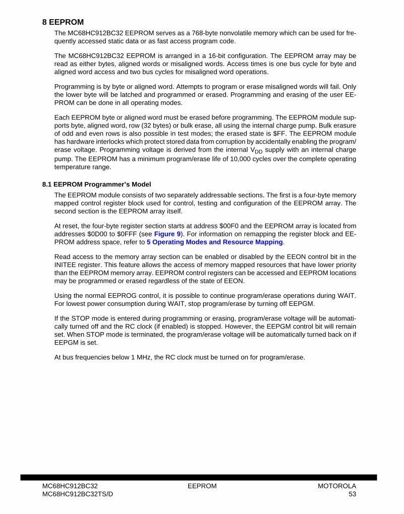
8 EEPROMThe MC68HC912BC32 EEPROM serves as a 768-byte nonvolatile memory which can be used for fre-quently accessed static data or as fast access program code.
The MC68HC912BC32 EEPROM is arranged in a 16-bit configuration. The EEPROM array may beread as either bytes, aligned words or misaligned words. Access times is one bus cycle for byte andaligned word access and two bus cycles for misaligned word operations.
Programming is by byte or aligned word. Attempts to program or erase misaligned words will fail. Onlythe lower byte will be latched and programmed or erased. Programming and erasing of the user EE-PROM can be done in all operating modes.
Each EEPROM byte or aligned word must be erased before programming. The EEPROM module sup-ports byte, aligned word, row (32 bytes) or bulk erase, all using the internal charge pump. Bulk erasureof odd and even rows is also possible in test modes; the erased state is $FF. The EEPROM modulehas hardware interlocks which protect stored data from corruption by accidentally enabling the program/erase voltage. Programming voltage is derived from the internal VDD supply with an internal chargepump. The EEPROM has a minimum program/erase life of 10,000 cycles over the complete operatingtemperature range.
8.1 EEPROM Programmer’s Model
The EEPROM module consists of two separately addressable sections. The first is a four-byte memorymapped control register block used for control, testing and configuration of the EEPROM array. Thesecond section is the EEPROM array itself.
At reset, the four-byte register section starts at address $00F0 and the EEPROM array is located fromaddresses $0D00 to $0FFF (see Figure 9). For information on remapping the register block and EE-PROM address space, refer to 5 Operating Modes and Resource Mapping.
Read access to the memory array section can be enabled or disabled by the EEON control bit in theINITEE register. This feature allows the access of memory mapped resources that have lower prioritythan the EEPROM memory array. EEPROM control registers can be accessed and EEPROM locationsmay be programmed or erased regardless of the state of EEON.
Using the normal EEPROG control, it is possible to continue program/erase operations during WAIT.For lowest power consumption during WAIT, stop program/erase by turning off EEPGM.
If the STOP mode is entered during programming or erasing, program/erase voltage will be automati-cally turned off and the RC clock (if enabled) is stopped. However, the EEPGM control bit will remainset. When STOP mode is terminated, the program/erase voltage will be automatically turned back on ifEEPGM is set.
At bus frequencies below 1 MHz, the RC clock must be turned on for program/erase.
MC68HC912BC32 EEPROM MOTOROLAMC68HC912BC32TS/D 53
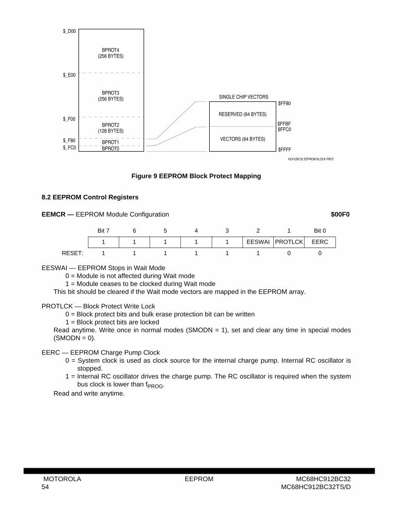
Figure 9 EEPROM Block Protect Mapping
8.2 EEPROM Control Registers
EEMCR — EEPROM Module Configuration $00F0
EESWAI — EEPROM Stops in Wait Mode0 = Module is not affected during Wait mode1 = Module ceases to be clocked during Wait mode
This bit should be cleared if the Wait mode vectors are mapped in the EEPROM array.
PROTLCK — Block Protect Write Lock0 = Block protect bits and bulk erase protection bit can be written1 = Block protect bits are locked
Read anytime. Write once in normal modes (SMODN = 1), set and clear any time in special modes(SMODN = 0).
EERC — EEPROM Charge Pump Clock0 = System clock is used as clock source for the internal charge pump. Internal RC oscillator is
stopped.1 = Internal RC oscillator drives the charge pump. The RC oscillator is required when the system
bus clock is lower than fPROG.Read and write anytime.
Bit 7 6 5 4 3 2 1 Bit 0
1 1 1 1 1 EESWAI PROTLCK EERC
RESET: 1 1 1 1 1 1 0 0
RESERVED (64 BYTES)
VECTORS (64 BYTES)
SINGLE CHIP VECTORS
HC912BC32 EEPROM BLOCK PROT
$FF80
$FFBF$FFC0
$FFFFBPROT0BPROT1
BPROT2
BPROT3
BPROT4
$_F00
$_E00
$_D00
$_F80$_FC0
(256 BYTES)
(256 BYTES)
(128 BYTES)
MOTOROLA EEPROM MC68HC912BC3254 MC68HC912BC32TS/D
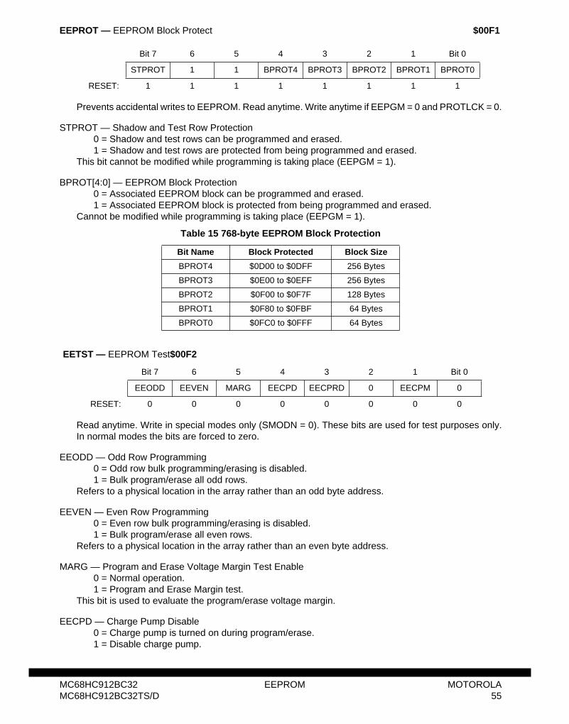
EEPROT — EEPROM Block Protect $00F1
Prevents accidental writes to EEPROM. Read anytime. Write anytime if EEPGM = 0 and PROTLCK = 0.
STPROT — Shadow and Test Row Protection0 = Shadow and test rows can be programmed and erased.1 = Shadow and test rows are protected from being programmed and erased.
This bit cannot be modified while programming is taking place (EEPGM = 1).
BPROT[4:0] — EEPROM Block Protection0 = Associated EEPROM block can be programmed and erased.1 = Associated EEPROM block is protected from being programmed and erased.
Cannot be modified while programming is taking place (EEPGM = 1).
Read anytime. Write in special modes only (SMODN = 0). These bits are used for test purposes only.In normal modes the bits are forced to zero.
EEODD — Odd Row Programming0 = Odd row bulk programming/erasing is disabled.1 = Bulk program/erase all odd rows.
Refers to a physical location in the array rather than an odd byte address.
EEVEN — Even Row Programming0 = Even row bulk programming/erasing is disabled.1 = Bulk program/erase all even rows.
Refers to a physical location in the array rather than an even byte address.
MARG — Program and Erase Voltage Margin Test Enable0 = Normal operation.1 = Program and Erase Margin test.
This bit is used to evaluate the program/erase voltage margin.
EECPD — Charge Pump Disable0 = Charge pump is turned on during program/erase.
Bit 7 6 5 4 3 2 1 Bit 0
STPROT 1 1 BPROT4 BPROT3 BPROT2 BPROT1 BPROT0
RESET: 1 1 1 1 1 1 1 1
Table 15 768-byte EEPROM Block Protection
Bit Name Block Protected Block Size
BPROT4 $0D00 to $0DFF 256 Bytes
BPROT3 $0E00 to $0EFF 256 Bytes
BPROT2 $0F00 to $0F7F 128 Bytes
BPROT1 $0F80 to $0FBF 64 Bytes
BPROT0 $0FC0 to $0FFF 64 Bytes
EETST — EEPROM Test$00F2
Bit 7 6 5 4 3 2 1 Bit 0
EEODD EEVEN MARG EECPD EECPRD 0 EECPM 0
RESET: 0 0 0 0 0 0 0 0
MC68HC912BC32 EEPROM MOTOROLAMC68HC912BC32TS/D 55
1 = Disable charge pump.
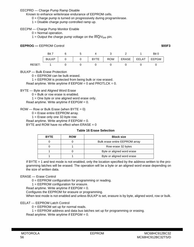
EECPRD — Charge Pump Ramp DisableKnown to enhance write/erase endurance of EEPROM cells.
0 = Charge pump is turned on progressively during program/erase.1 = Disable charge pump controlled ramp up.
EECPM — Charge Pump Monitor Enable0 = Normal operation.1 = Output the charge pump voltage on the IRQ/VPP pin.
EEPROG — EEPROM Control $00F3
BULKP — Bulk Erase Protection0 = EEPROM can be bulk erased.1 = EEPROM is protected from being bulk or row erased.
Read anytime. Write anytime if EEPGM = 0 and PROTLCK = 0.
BYTE — Byte and Aligned Word Erase0 = Bulk or row erase is enabled.1 = One byte or one aligned word erase only.
Read anytime. Write anytime if EEPGM = 0.
ROW — Row or Bulk Erase (when BYTE = 0)0 = Erase entire EEPROM array.1 = Erase only one 32-byte row.
Read anytime. Write anytime if EEPGM = 0.BYTE and ROW have no effect when ERASE = 0
If BYTE = 1 and test mode is not enabled, only the location specified by the address written to the pro-gramming latches will be erased. The operation will be a byte or an aligned word erase depending onthe size of written data.
ERASE — Erase Control0 = EEPROM configuration for programming or reading.1 = EEPROM configuration for erasure.
Read anytime. Write anytime if EEPGM = 0.Configures the EEPROM for erasure or programming.When test mode is not enabled and unless BULKP is set, erasure is by byte, aligned word, row or bulk.
EELAT — EEPROM Latch Control0 = EEPROM set up for normal reads.1 = EEPROM address and data bus latches set up for programming or erasing.
Read anytime. Write anytime if EEPGM = 0.
Bit 7 6 5 4 3 2 1 Bit 0
BULKP 0 0 BYTE ROW ERASE EELAT EEPGM
RESET: 1 0 0 0 0 0 0 0
Table 16 Erase Selection
BYTE ROW Block size
0 0 Bulk erase entire EEPROM array
0 1 Row erase 32 bytes
1 0 Byte or aligned word erase
1 1 Byte or aligned word erase
MOTOROLA EEPROM MC68HC912BC3256 MC68HC912BC32TS/D
NOTEWhen EELAT is set, the entire EEPROM is unavailable for reads, therefore no pro-gram residing in the EEPROM can be executed while attempting to program un-used EEPROM space. Care should be taken that no references to the EEPROMare used while programming. Interrupts should be turned off if the vectors are inthe EEPROM. Timing and any serial communications must be done with pollingduring the programming process.
BYTE, ROW, ERASE and EELAT bits can be written simultaneously or in any sequence.
EEPGM — Program and Erase Enable0 = Disables program/erase voltage to EEPROM.1 = Applies program/erase voltage to EEPROM.
The EEPGM bit can be set only after EELAT has been set. When an attempt is made to set EELAT andEEPGM simultaneously, EEPGM remains clear but EELAT is set.The BULKP, BYTE, ROW, ERASE and EELAT bits cannot be changed when EEPGM is set. To com-plete a program or erase, two successive writes to clear EEPGM and EELAT bits are required beforereading the programmed data. A write to an EEPROM location has no effect when EEPGM is set.Latched address and data cannot be modified during program or erase.
A program or erase operation should follow the sequence below:
1. Write BYTE, ROW and ERASE to the desired value, write EELAT = 12. Write a byte or an aligned word to an EEPROM address3. Write EEPGM = 14. Wait for programming (tPROG) or erase (tERASE) delay time5. Write EEPGM = 06. Write EELAT = 0
It is possible to program/erase more bytes or words without intermediate EEPROM reads, by jumpingfrom step 5 to step 2.
MC68HC912BC32 EEPROM MOTOROLAMC68HC912BC32TS/D 57

MOTOROLA EEPROM MC68HC912BC3258 MC68HC912BC32TS/D
9 Resets and InterruptsCPU12 exceptions include resets and interrupts. Each exception has an associated 16-bit vector, whichpoints to the memory location where the routine that handles the exception is located. Vectors arestored in the upper 128 bytes of the standard 64K byte address map.
The six highest vector addresses are used for resets and non-maskable interrupt sources. The remain-der of the vectors are used for maskable interrupts, and all must be initialized to point to the address ofthe appropriate service routine.
9.1 Exception Priority
A hardware priority hierarchy determines which reset or interrupt is serviced first when simultaneousrequests are made. Six sources are not maskable. The remaining sources are maskable, and any oneof them can be given priority over other maskable interrupts.
The priorities of the non-maskable sources are:
1. POR or RESET pin2. Clock monitor reset3. COP watchdog reset4. Unimplemented instruction trap5. Software interrupt instruction (SWI)6. XIRQ signal (if X bit in CCR = 0)
9.2 Maskable interrupts
Maskable interrupt sources include on-chip peripheral systems and external interrupt service requests.Interrupts from these sources are recognized when the global interrupt mask bit (I) in the CCR iscleared. The default state of the I bit out of reset is one, but it can be written at any time.
Interrupt sources are prioritized by default but any one maskable interrupt source may be assigned thehighest priority by means of the HPRIO register. The relative priorities of the other sources remain thesame.
An interrupt that is assigned highest priority is still subject to global masking by the I bit in the CCR, orby any associated local bits. Interrupt vectors are not affected by priority assignment. HPRIO can onlybe written while the I bit is set (interrupts inhibited). Table 17 lists interrupt sources and vectors in defaultorder of priority.
MC68HC912BC32 Resets and Interrupts MOTOROLAMC68HC912BC32TS/D 59
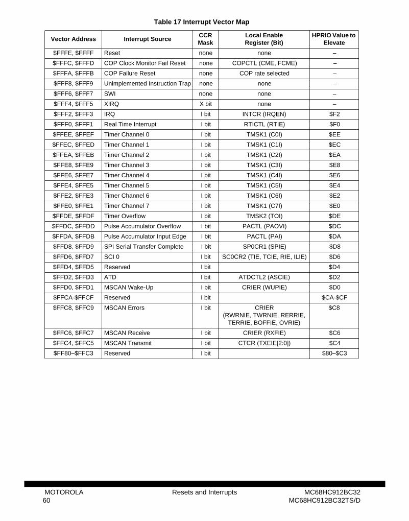
Table 17 Interrupt Vector Map
Vector Address Interrupt SourceCCR Mask
Local EnableRegister (Bit)
HPRIO Value to Elevate
$FFFE, $FFFF Reset none none –
$FFFC, $FFFD COP Clock Monitor Fail Reset none COPCTL (CME, FCME) –
$FFFA, $FFFB COP Failure Reset none COP rate selected –
$FFF8, $FFF9 Unimplemented Instruction Trap none none –
$FFF6, $FFF7 SWI none none –
$FFF4, $FFF5 XIRQ X bit none –
$FFF2, $FFF3 IRQ I bit INTCR (IRQEN) $F2
$FFF0, $FFF1 Real Time Interrupt I bit RTICTL (RTIE) $F0
$FFEE, $FFEF Timer Channel 0 I bit TMSK1 (C0I) $EE
$FFEC, $FFED Timer Channel 1 I bit TMSK1 (C1I) $EC
$FFEA, $FFEB Timer Channel 2 I bit TMSK1 (C2I) $EA
$FFE8, $FFE9 Timer Channel 3 I bit TMSK1 (C3I) $E8
$FFE6, $FFE7 Timer Channel 4 I bit TMSK1 (C4I) $E6
$FFE4, $FFE5 Timer Channel 5 I bit TMSK1 (C5I) $E4
$FFE2, $FFE3 Timer Channel 6 I bit TMSK1 (C6I) $E2
$FFE0, $FFE1 Timer Channel 7 I bit TMSK1 (C7I) $E0
$FFDE, $FFDF Timer Overflow I bit TMSK2 (TOI) $DE
$FFDC, $FFDD Pulse Accumulator Overflow I bit PACTL (PAOVI) $DC
$FFDA, $FFDB Pulse Accumulator Input Edge I bit PACTL (PAI) $DA
$FFD8, $FFD9 SPI Serial Transfer Complete I bit SP0CR1 (SPIE) $D8
$FFD6, $FFD7 SCI 0 I bit SC0CR2 (TIE, TCIE, RIE, ILIE) $D6
$FFD4, $FFD5 Reserved I bit $D4
$FFD2, $FFD3 ATD I bit ATDCTL2 (ASCIE) $D2
$FFD0, $FFD1 MSCAN Wake-Up I bit CRIER (WUPIE) $D0
$FFCA-$FFCF Reserved I bit $CA-$CF
$FFC8, $FFC9 MSCAN Errors I bit CRIER(RWRNIE, TWRNIE, RERRIE,
TERRIE, BOFFIE, OVRIE)
$C8
$FFC6, $FFC7 MSCAN Receive I bit CRIER (RXFIE) $C6
$FFC4, $FFC5 MSCAN Transmit I bit CTCR (TXEIE[2:0]) $C4
$FF80–$FFC3 Reserved I bit $80–$C3
MOTOROLA Resets and Interrupts MC68HC912BC3260 MC68HC912BC32TS/D
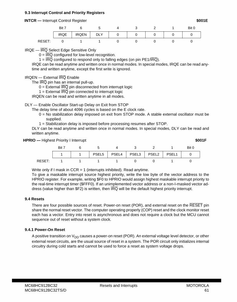
9.3 Interrupt Control and Priority Registers
IRQE — IRQ Select Edge Sensitive Only0 = IRQ configured for low-level recognition.1 = IRQ configured to respond only to falling edges (on pin PE1/IRQ).
IRQE can be read anytime and written once in normal modes. In special modes, IRQE can be read any-time and written anytime, except the first write is ignored.
IRQEN — External IRQ EnableThe IRQ pin has an internal pull-up.
0 = External IRQ pin disconnected from interrupt logic1 = External IRQ pin connected to interrupt logic
IRQEN can be read and written anytime in all modes.
DLY — Enable Oscillator Start-up Delay on Exit from STOPThe delay time of about 4096 cycles is based on the E clock rate.
0 = No stabilization delay imposed on exit from STOP mode. A stable external oscillator must besupplied.
1 = Stabilization delay is imposed before processing resumes after STOP.DLY can be read anytime and written once in normal modes. In special modes, DLY can be read andwritten anytime.
Write only if I mask in CCR = 1 (interrupts inhibited). Read anytime.To give a maskable interrupt source highest priority, write the low byte of the vector address to theHPRIO register. For example, writing $F0 to HPRIO would assign highest maskable interrupt priority tothe real-time interrupt timer ($FFF0). If an unimplemented vector address or a non-I-masked vector ad-dress (value higher than $F2) is written, then IRQ will be the default highest priority interrupt.
9.4 Resets
There are four possible sources of reset. Power-on reset (POR), and external reset on the RESET pinshare the normal reset vector. The computer operating properly (COP) reset and the clock monitor reseteach has a vector. Entry into reset is asynchronous and does not require a clock but the MCU cannotsequence out of reset without a system clock.
9.4.1 Power-On Reset
A positive transition on VDD causes a power-on reset (POR). An external voltage level detector, or otherexternal reset circuits, are the usual source of reset in a system. The POR circuit only initializes internalcircuitry during cold starts and cannot be used to force a reset as system voltage drops.
INTCR — Interrupt Control Register $001E
Bit 7 6 5 4 3 2 1 Bit 0
IRQE IRQEN DLY 0 0 0 0 0
RESET: 0 1 1 0 0 0 0 0
HPRIO — Highest Priority I Interrupt $001F
Bit 7 6 5 4 3 2 1 Bit 0
1 1 PSEL5 PSEL4 PSEL3 PSEL2 PSEL1 0
RESET: 1 1 1 1 0 0 1 0
MC68HC912BC32 Resets and Interrupts MOTOROLAMC68HC912BC32TS/D 61
9.4.2 External Reset
The CPU distinguishes between internal and external reset conditions by sensing whether the reset pinrises to a logic one in less than eight E-clock cycles after an internal device releases reset. When a resetcondition is sensed, the RESET pin is driven low by an internal device for about 16 E-clock cycles, thenreleased. Eight E-clock cycles later it is sampled. If the pin is still held low, the CPU assumes that anexternal reset has occurred. If the pin is high, it indicates that the reset was initiated internally by eitherthe COP system or the clock monitor.
To prevent a COP or clock monitor reset from being detected during an external reset, hold the resetpin low for at least 32 cycles. An external RC power-up delay circuit on the reset pin is not recommended— circuit charge time can cause the MCU to misinterpret the type of reset that has occurred.
9.4.3 COP Reset
The MCU includes a computer operating properly (COP) system to help protect against software fail-ures. When COP is enabled, software must write $55 and $AA (in this order) to the COPRST registerin order to keep a watchdog timer from timing out. Other instructions may be executed between thesewrites. A write of any value other than $55 or $AA or software failing to execute the sequence properlycauses a COP reset to occur.
9.4.4 Clock Monitor Reset
If clock frequency falls below a predetermined limit when the clock monitor is enabled, a reset occurs.
9.5 Effects of Reset
When a reset occurs, MCU registers and control bits are changed to known start-up states, as follows.
9.5.1 Operating Mode and Memory Map
Operating mode and default memory mapping are determined by the states of the BKGD, MODA, andMODB pins during reset. The SMODN, MODA, and MODB bits in the MODE register reflect the statusof the mode-select inputs at the rising edge of reset. Operating mode and default maps can subsequent-ly be changed according to strictly defined rules.
9.5.2 Clock and Watchdog Control Logic
The COP watchdog system is enabled, with the CR [2:0] bits set for the shortest duration time-out. Theclock monitor is disabled. The RTIF flag is cleared and automatic hardware interrupts are masked. Therate control bits are cleared, and must be initialized before the RTI system is used. The DLY control bitis set to specify an oscillator start-up delay upon recovery from STOP mode.
9.5.3 Interrupts
PSEL is initialized in the HPRIO register with the value $F2, causing the external IRQ pin to have thehighest I-bit interrupt priority. The IRQ pin is configured for level-sensitive operation (for wired-OR sys-tems). However, the interrupt mask bits in the CPU12 CCR are set to mask X and I related interruptrequests.
9.5.4 Parallel I/O
If the MCU comes out of reset in an expanded mode, port A and port B are used for the multiplexedaddress/data bus and port E pins are normally used to control the external bus (operation of port E pinscan be affected by the PEAR register). If the MCU comes out of reset in a single-chip mode, all portsare configured as general-purpose high-impedance inputs. Port S, port T, port DLC, port P, and port ADare all configured as general-purpose inputs.
MOTOROLA Resets and Interrupts MC68HC912BC3262 MC68HC912BC32TS/D
9.5.5 Central Processing Unit
After reset, the CPU fetches a vector from the appropriate address, then begins executing instructions.The stack pointer and other CPU registers are indeterminate immediately after reset. The CCR X andI interrupt mask bits are set to mask any interrupt requests. The S bit is also set to inhibit the STOPinstruction.
9.5.6 Memory
After reset, the internal register block is located at $0000–$01FF, the register-following space is at$0200–$03FF, and RAM is at $0800–$0BFF. EEPROM is located at $0D00–$0FFF. Flash EEPROMis located at $8000–$FFFF in single-chip modes and at $0000–$7FFF (but disabled) in expandedmodes.
9.5.7 Other Resources
The timer, serial communications interface (SCI), serial peripheral interface (SPI), CAN controller(MSCAN12), pulse-width modulator (PWM), and analog-to-digital converter (ATD) are off after reset.
9.6 Register Stacking
Once enabled, an interrupt request can be recognized at any time after the I bit in the CCR is cleared.When an interrupt service request is recognized, the CPU responds at the completion of the instructionbeing executed. Interrupt latency varies according to the number of cycles required to complete the in-struction. Some of the longer instructions can be interrupted and will resume normally after servicingthe interrupt.
When the CPU begins to service an interrupt, the instruction queue is cleared, the return address is cal-culated, and then it and the contents of the CPU registers are stacked as shown in Table 18.
After the CCR is stacked, the I bit (and the X bit, if an XIRQ interrupt service request is pending) is setto prevent other interrupts from disrupting the interrupt service routine. The interrupt vector for the high-est priority source that was pending at the beginning of the interrupt sequence is fetched, and executioncontinues at the referenced location. At the end of the interrupt service routine, an RTI instruction re-stores the content of all registers from information on the stack, and normal program execution re-sumes. If another interrupt is pending at the end of an interrupt service routine, the register unstackingand restacking is bypassed and the vector of the pending interrupt is fetched.
Table 18 Stacking Order on Entry to Interrupts
Memory Location CPU Registers
SP – 2 RTNH : RTNL
SP – 4 YH : YL
SP – 6 XH : XL
SP – 8 B : A
SP – 9 CCR
MC68HC912BC32 Resets and Interrupts MOTOROLAMC68HC912BC32TS/D 63

MOTOROLA Resets and Interrupts MC68HC912BC3264 MC68HC912BC32TS/D
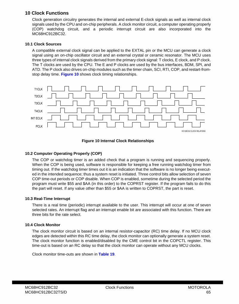
10 Clock FunctionsClock generation circuitry generates the internal and external E-clock signals as well as internal clocksignals used by the CPU and on-chip peripherals. A clock monitor circuit, a computer operating properly(COP) watchdog circuit, and a periodic interrupt circuit are also incorporated into theMC68HC912BC32.
10.1 Clock Sources
A compatible external clock signal can be applied to the EXTAL pin or the MCU can generate a clocksignal using an on-chip oscillator circuit and an external crystal or ceramic resonator. The MCU usesthree types of internal clock signals derived from the primary clock signal: T clocks, E clock, and P clock.The T clocks are used by the CPU. The E and P clocks are used by the bus interfaces, BDM, SPI, andATD. The P clock also drives on-chip modules such as the timer chain, SCI, RTI, COP, and restart-from-stop delay time. Figure 10 shows clock timing relationships.
Figure 10 Internal Clock Relationships
10.2 Computer Operating Properly (COP)
The COP or watchdog timer is an added check that a program is running and sequencing properly.When the COP is being used, software is responsible for keeping a free running watchdog timer fromtiming out. If the watchdog timer times out it is an indication that the software is no longer being execut-ed in the intended sequence; thus a system reset is initiated. Three control bits allow selection of sevenCOP time-out periods or COP disable. When COP is enabled, sometime during the selected period theprogram must write $55 and $AA (in this order) to the COPRST register. If the program fails to do thisthe part will reset. If any value other than $55 or $AA is written to COPRST, the part is reset.
10.3 Real-Time Interrupt
There is a real time (periodic) interrupt available to the user. This interrupt will occur at one of sevenselected rates. An interrupt flag and an interrupt enable bit are associated with this function. There arethree bits for the rate select.
10.4 Clock Monitor
The clock monitor circuit is based on an internal resistor-capacitor (RC) time delay. If no MCU clockedges are detected within this RC time delay, the clock monitor can optionally generate a system reset.The clock monitor function is enabled/disabled by the CME control bit in the COPCTL register. Thistime-out is based on an RC delay so that the clock monitor can operate without any MCU clocks.
Clock monitor time-outs are shown in Table 19.
T1CLK
T2CLK
T3CLK
T4CLK
INT ECLK
PCLKHC12BC32 CLOCK RELATIONS
MC68HC912BC32 Clock Functions MOTOROLAMC68HC912BC32TS/D 65
10.5 Clock Function Registers
All register addresses shown reflect the reset state. Registers may be mapped to any 2-Kbyte space.
RTIE — Real Time Interrupt EnableRead and write anytime.
0 = Interrupt requests from RTI are disabled.1 = Interrupt will be requested whenever RTIF is set.
RSWAI — RTI and COP Stop While in WaitWrite once in normal modes, anytime in special modes. Read anytime.
0 = Allows the RTI and COP to continue running in wait.1 = Disables both the RTI and COP whenever the part goes into Wait.
RSBCK — RTI and COP Stop While in Background Debug ModeWrite once in normal modes, anytime in special modes. Read anytime.
0 = Allows the RTI and COP to continue running while in background mode.1 = Disables both the RTI and COP whenever the part is in background mode. This is useful for
emulation.
RTBYP — Real Time Interrupt Divider Chain BypassWrite not allowed in normal modes, anytime in special modes. Read anytime.
0 = Divider chain functions normally.
1 = Divider chain is bypassed, allows faster testing (the divider chain is normally P divided by 213,when bypassed becomes P divided by 4).
RTR2, RTR1, RTR0 — Real-Time Interrupt Rate SelectRead and write anytime.Rate select for real-time interrupt. The clock used for this module is the E clock.
Table 19 Clock Monitor Time-Outs
Supply Range
5V +/− 10% 2-20 µS
3V +/− 10% 5-100 µS
RTICTL — Real-Time Interrupt Control Register $0014
Bit 7 6 5 4 3 2 1 Bit 0
RTIE RSWAI RSBCK 0 RTBYP RTR2 RTR1 RTR0
RESET: 0 0 0 0 0 0 0 0
MOTOROLA Clock Functions MC68HC912BC3266 MC68HC912BC32TS/D
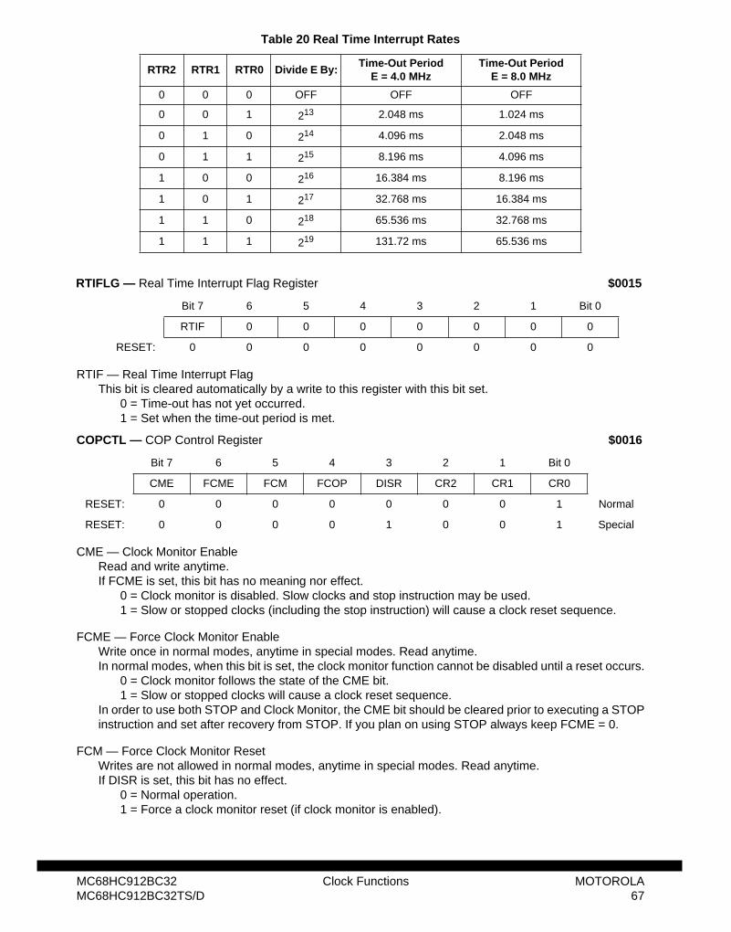
RTIF — Real Time Interrupt FlagThis bit is cleared automatically by a write to this register with this bit set.
0 = Time-out has not yet occurred.1 = Set when the time-out period is met.
CME — Clock Monitor EnableRead and write anytime.If FCME is set, this bit has no meaning nor effect.
0 = Clock monitor is disabled. Slow clocks and stop instruction may be used.1 = Slow or stopped clocks (including the stop instruction) will cause a clock reset sequence.
FCME — Force Clock Monitor Enable Write once in normal modes, anytime in special modes. Read anytime.In normal modes, when this bit is set, the clock monitor function cannot be disabled until a reset occurs.
0 = Clock monitor follows the state of the CME bit.1 = Slow or stopped clocks will cause a clock reset sequence.
In order to use both STOP and Clock Monitor, the CME bit should be cleared prior to executing a STOPinstruction and set after recovery from STOP. If you plan on using STOP always keep FCME = 0.
FCM — Force Clock Monitor ResetWrites are not allowed in normal modes, anytime in special modes. Read anytime.If DISR is set, this bit has no effect.
0 = Normal operation.1 = Force a clock monitor reset (if clock monitor is enabled).
Table 20 Real Time Interrupt Rates
RTR2 RTR1 RTR0 Divide E By:Time-Out Period
E = 4.0 MHzTime-Out Period
E = 8.0 MHz
0 0 0 OFF OFF OFF
0 0 1 213 2.048 ms 1.024 ms
0 1 0 214 4.096 ms 2.048 ms
0 1 1 215 8.196 ms 4.096 ms
1 0 0 216 16.384 ms 8.196 ms
1 0 1 217 32.768 ms 16.384 ms
1 1 0 218 65.536 ms 32.768 ms
1 1 1 219 131.72 ms 65.536 ms
RTIFLG — Real Time Interrupt Flag Register $0015
Bit 7 6 5 4 3 2 1 Bit 0
RTIF 0 0 0 0 0 0 0
RESET: 0 0 0 0 0 0 0 0
COPCTL — COP Control Register $0016
Bit 7 6 5 4 3 2 1 Bit 0
CME FCME FCM FCOP DISR CR2 CR1 CR0
RESET: 0 0 0 0 0 0 0 1 Normal
RESET: 0 0 0 0 1 0 0 1 Special
MC68HC912BC32 Clock Functions MOTOROLAMC68HC912BC32TS/D 67
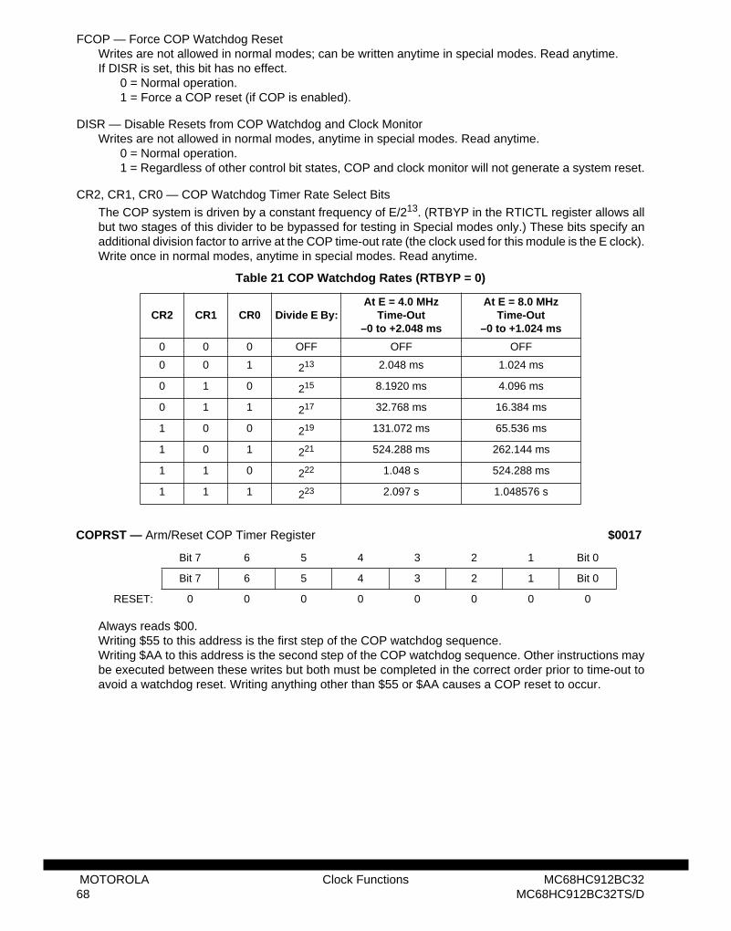
FCOP — Force COP Watchdog ResetWrites are not allowed in normal modes; can be written anytime in special modes. Read anytime.If DISR is set, this bit has no effect.
0 = Normal operation.1 = Force a COP reset (if COP is enabled).
DISR — Disable Resets from COP Watchdog and Clock MonitorWrites are not allowed in normal modes, anytime in special modes. Read anytime.
0 = Normal operation.1 = Regardless of other control bit states, COP and clock monitor will not generate a system reset.
CR2, CR1, CR0 — COP Watchdog Timer Rate Select Bits
The COP system is driven by a constant frequency of E/213. (RTBYP in the RTICTL register allows allbut two stages of this divider to be bypassed for testing in Special modes only.) These bits specify anadditional division factor to arrive at the COP time-out rate (the clock used for this module is the E clock).Write once in normal modes, anytime in special modes. Read anytime.
Always reads $00. Writing $55 to this address is the first step of the COP watchdog sequence.Writing $AA to this address is the second step of the COP watchdog sequence. Other instructions maybe executed between these writes but both must be completed in the correct order prior to time-out toavoid a watchdog reset. Writing anything other than $55 or $AA causes a COP reset to occur.
Table 21 COP Watchdog Rates (RTBYP = 0)
CR2 CR1 CR0 Divide E By:At E = 4.0 MHz
Time-Out–0 to +2.048 ms
At E = 8.0 MHzTime-Out
–0 to +1.024 ms
0 0 0 OFF OFF OFF
0 0 1 213 2.048 ms 1.024 ms
0 1 0 215 8.1920 ms 4.096 ms
0 1 1 217 32.768 ms 16.384 ms
1 0 0 219 131.072 ms 65.536 ms
1 0 1 221 524.288 ms 262.144 ms
1 1 0 222 1.048 s 524.288 ms
1 1 1 223 2.097 s 1.048576 s
COPRST — Arm/Reset COP Timer Register $0017
Bit 7 6 5 4 3 2 1 Bit 0
Bit 7 6 5 4 3 2 1 Bit 0
RESET: 0 0 0 0 0 0 0 0
MOTOROLA Clock Functions MC68HC912BC3268 MC68HC912BC32TS/D
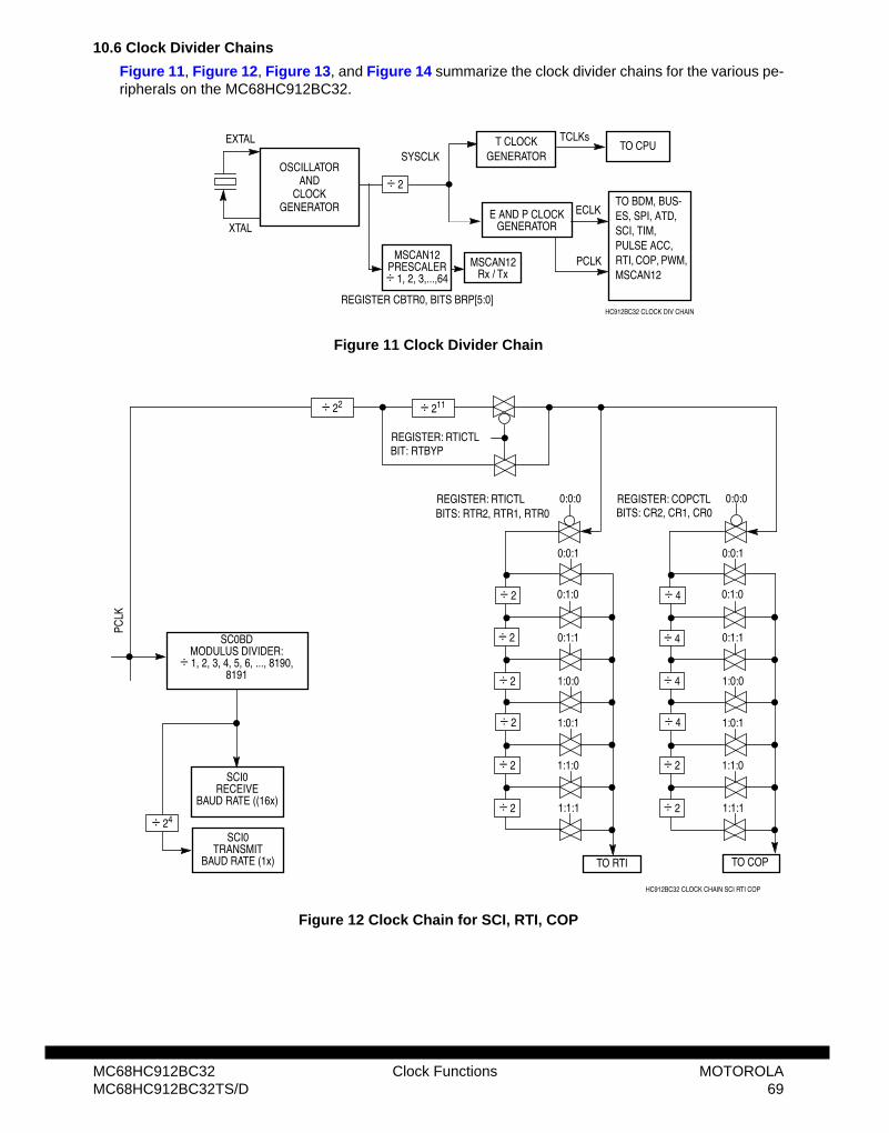
10.6 Clock Divider Chains
Figure 11, Figure 12, Figure 13, and Figure 14 summarize the clock divider chains for the various pe-ripherals on the MC68HC912BC32.
Figure 11 Clock Divider Chain
Figure 12 Clock Chain for SCI, RTI, COP
OSCILLATORAND
CLOCKGENERATOR
EXTAL
XTAL
SYSCLKT CLOCK
GENERATORTO CPU
E AND P CLOCKGENERATOR
ECLK
PCLK
TO BDM, BUS-ES, SPI, ATD, SCI, TIM, PULSE ACC, RTI, COP, PWM, MSCAN12
TCLKs
HC912BC32 CLOCK DIV CHAIN
÷ 2
MSCAN12PRESCALER÷ 1, 2, 3,...,64
MSCAN12Rx / Tx
REGISTER CBTR0, BITS BRP[5:0]
PCLK
SC0BDMODULUS DIVIDER:
÷ 1, 2, 3, 4, 5, 6, ..., 8190, 8191
SCI0RECEIVE
BAUD RATE ((16x)
SCI0TRANSMIT
BAUD RATE (1x)
BITS: RTR2, RTR1, RTR0
TO RTI
BITS: CR2, CR1, CR0
TO COP
÷ 24
0:0:0
0:0:1
0:1:0
0:1:1
1:0:0
1:0:1
1:1:0
1:1:1
÷ 2
÷ 2
÷ 2
÷ 2
÷ 2
÷ 2
0:0:0
0:0:1
0:1:0
0:1:1
1:0:0
1:0:1
1:1:0
1:1:1
÷ 4
÷ 4
÷ 4
÷ 2
÷ 4
÷ 2
REGISTER: COPCTLREGISTER: RTICTL
HC912BC32 CLOCK CHAIN SCI RTI COP
÷ 211÷ 22
BIT: RTBYPREGISTER: RTICTL
MC68HC912BC32 Clock Functions MOTOROLAMC68HC912BC32TS/D 69
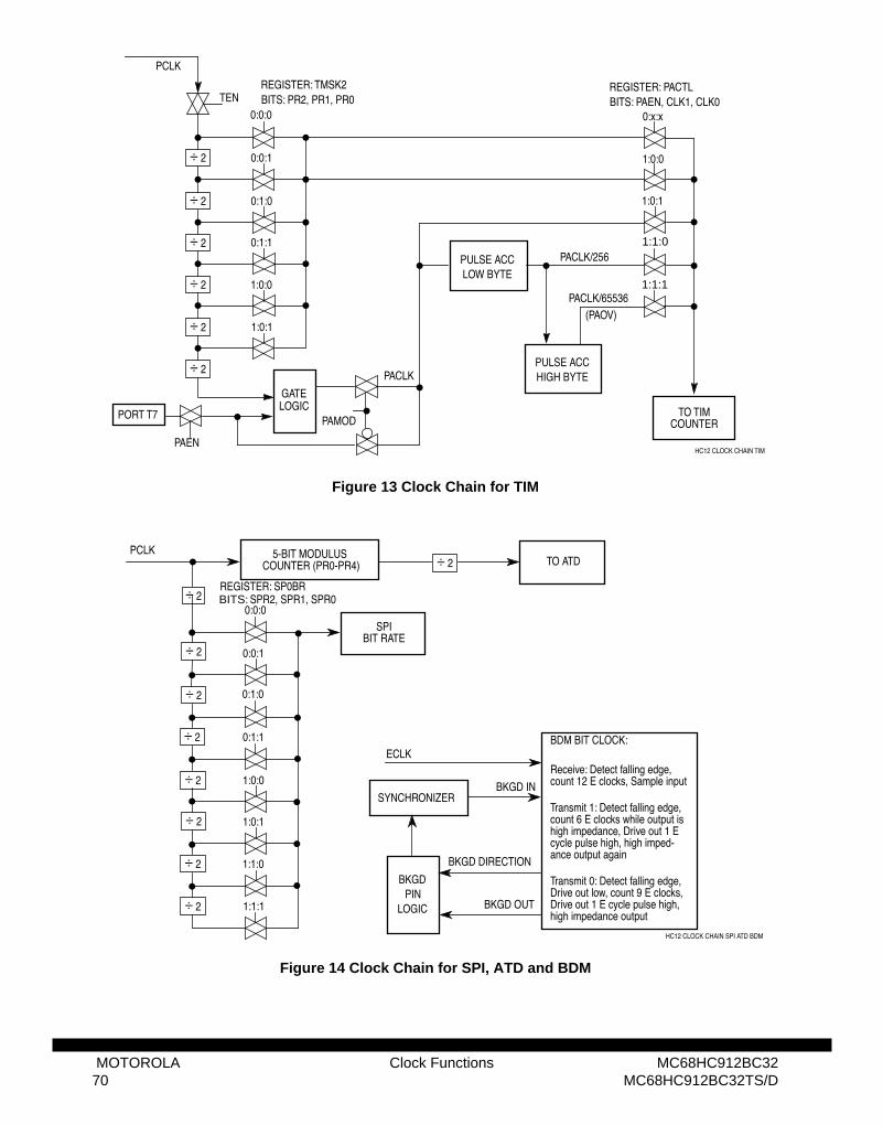
Figure 13 Clock Chain for TIM
Figure 14 Clock Chain for SPI, ATD and BDM
BITS: PR2, PR1, PR0
PCLK
1:0:0
1:0:1
1:1:0
1:1:1
TO TIM COUNTER
PORT T7 PAMOD
PACLK
PULSE ACCLOW BYTE
PACLK/256
PULSE ACCHIGH BYTE
PACLK/65536(PAOV)
GATELOGIC
BITS: PAEN, CLK1, CLK00:x:x
TEN
PAEN
0:0:0
0:0:1
0:1:0
0:1:1
1:0:0
1:0:1
÷ 2
÷ 2
÷ 2
÷ 2
÷ 2
÷ 2
REGISTER: PACTLREGISTER: TMSK2
HC12 CLOCK CHAIN TIM
PCLK
BITS: SPR2, SPR1, SPR0
SPI BIT RATE
5-BIT MODULUS COUNTER (PR0-PR4) TO ATD
ECLK
BKGD
BDM BIT CLOCK:
Receive: Detect falling edge, count 12 E clocks, Sample input
Transmit 1: Detect falling edge, count 6 E clocks while output is high impedance, Drive out 1 E cycle pulse high, high imped-ance output again
Transmit 0: Detect falling edge, Drive out low, count 9 E clocks, Drive out 1 E cycle pulse high, high impedance output
PIN
SYNCHRONIZER
LOGIC
BKGD IN
BKGD OUT
BKGD DIRECTION
÷ 2
0:0:0
0:0:1
0:1:0
0:1:1
1:0:0
1:0:1
1:1:0
1:1:1
÷ 2
÷ 2
÷ 2
÷ 2
÷ 2
÷ 2
÷ 2
÷ 2REGISTER: SP0BR
HC12 CLOCK CHAIN SPI ATD BDM
MOTOROLA Clock Functions MC68HC912BC3270 MC68HC912BC32TS/D
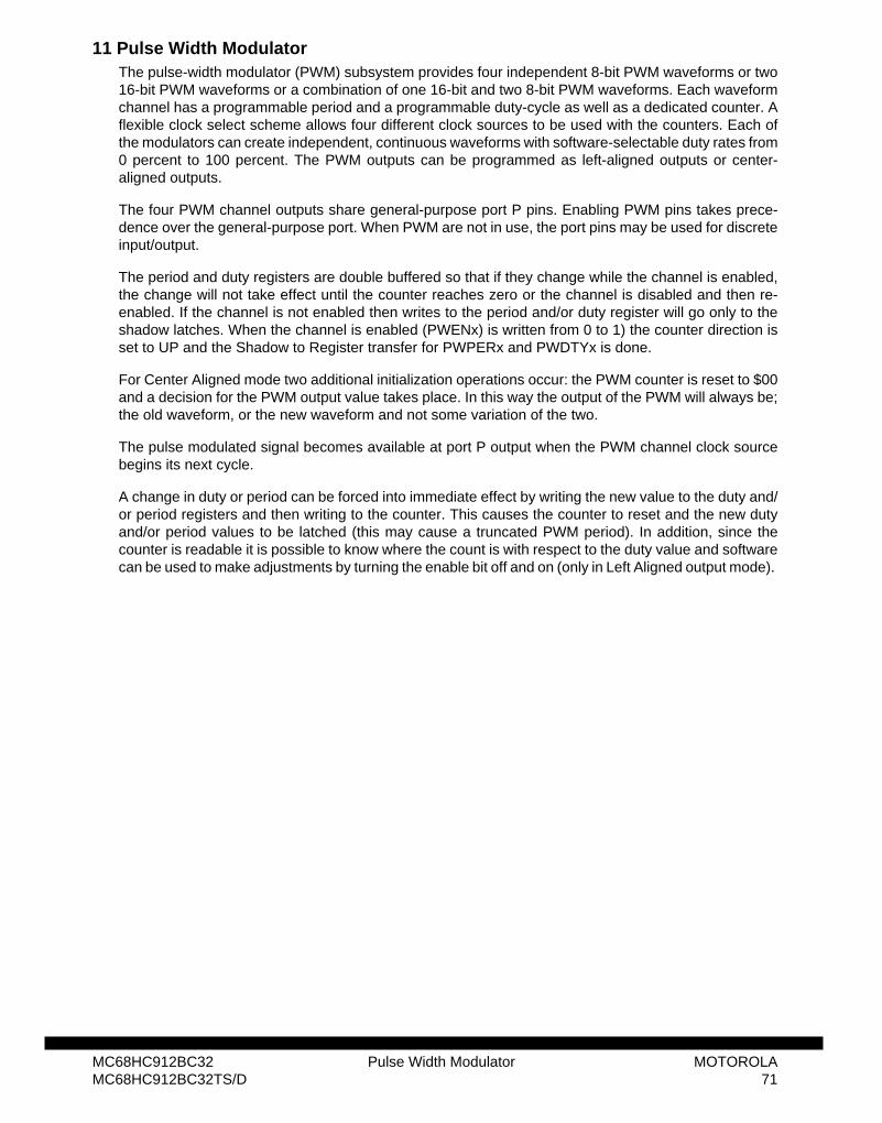
11 Pulse Width ModulatorThe pulse-width modulator (PWM) subsystem provides four independent 8-bit PWM waveforms or two16-bit PWM waveforms or a combination of one 16-bit and two 8-bit PWM waveforms. Each waveformchannel has a programmable period and a programmable duty-cycle as well as a dedicated counter. Aflexible clock select scheme allows four different clock sources to be used with the counters. Each ofthe modulators can create independent, continuous waveforms with software-selectable duty rates from0 percent to 100 percent. The PWM outputs can be programmed as left-aligned outputs or center-aligned outputs.
The four PWM channel outputs share general-purpose port P pins. Enabling PWM pins takes prece-dence over the general-purpose port. When PWM are not in use, the port pins may be used for discreteinput/output.
The period and duty registers are double buffered so that if they change while the channel is enabled,the change will not take effect until the counter reaches zero or the channel is disabled and then re-enabled. If the channel is not enabled then writes to the period and/or duty register will go only to theshadow latches. When the channel is enabled (PWENx) is written from 0 to 1) the counter direction isset to UP and the Shadow to Register transfer for PWPERx and PWDTYx is done.
For Center Aligned mode two additional initialization operations occur: the PWM counter is reset to $00and a decision for the PWM output value takes place. In this way the output of the PWM will always be;the old waveform, or the new waveform and not some variation of the two.
The pulse modulated signal becomes available at port P output when the PWM channel clock sourcebegins its next cycle.
A change in duty or period can be forced into immediate effect by writing the new value to the duty and/or period registers and then writing to the counter. This causes the counter to reset and the new dutyand/or period values to be latched (this may cause a truncated PWM period). In addition, since thecounter is readable it is possible to know where the count is with respect to the duty value and softwarecan be used to make adjustments by turning the enable bit off and on (only in Left Aligned output mode).
MC68HC912BC32 Pulse Width Modulator MOTOROLAMC68HC912BC32TS/D 71
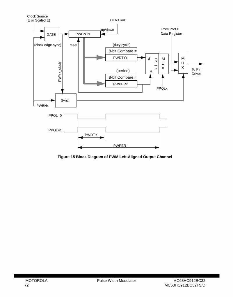
Figure 15 Block Diagram of PWM Left-Aligned Output Channel
(duty cycle)
Clock Source(E or Scaled E)
reset
S
R
Q
Q
MUX
PPOLx
From Port PData Register
PWENx
PWDTY
PWPER
(clock edge sync)
To PinDriver
PWCNTxGATE
8-bit Compare =
PWDTYx
(period)
8-bit Compare =
PWPERx
MUX
CENTR=0
up/down
PPOL=0
PPOL=1
Sync
PW
Mx_
cloc
k
MOTOROLA Pulse Width Modulator MC68HC912BC3272 MC68HC912BC32TS/D
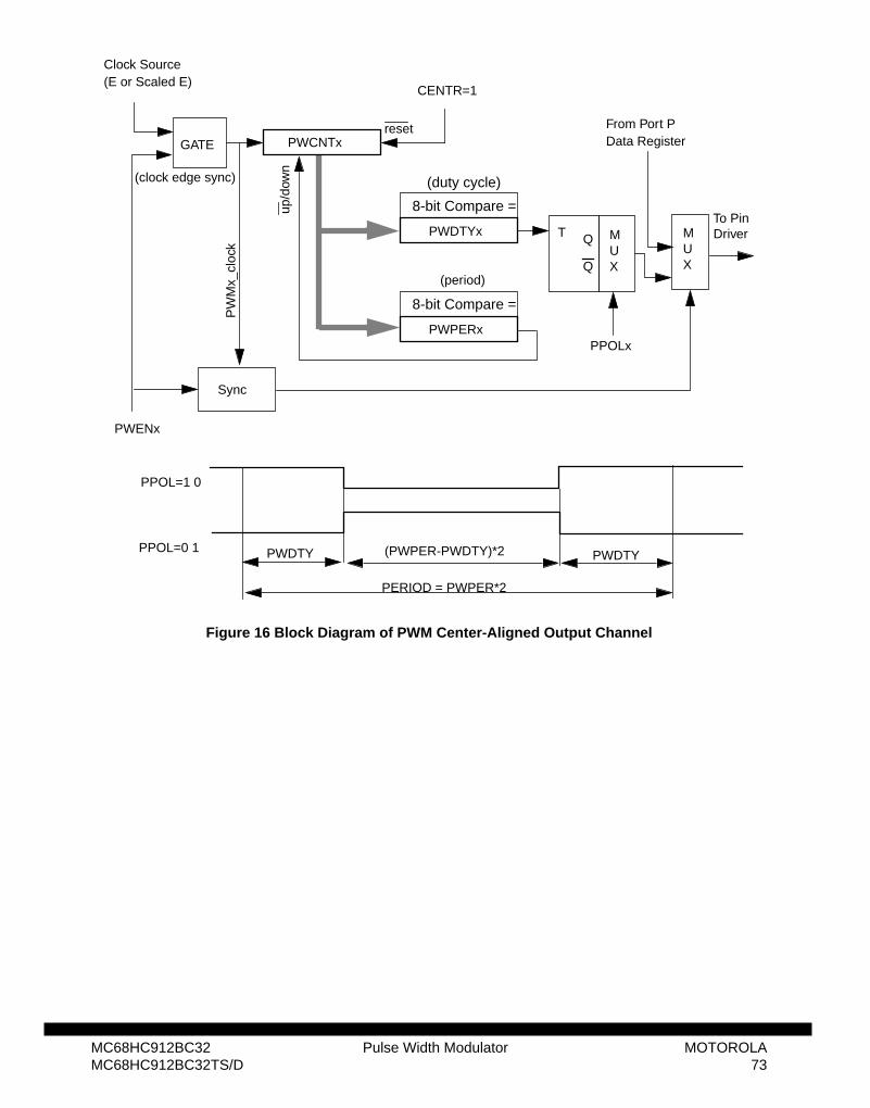
Figure 16 Block Diagram of PWM Center-Aligned Output Channel
PERIOD = PWPER*2
(PWPER-PWDTY)*2
(duty cycle)
Clock Source(E or Scaled E)
Q
Q
MUX
PPOLx
From Port PData Register
(clock edge sync)
To PinDriver
PWCNTxGATE
8-bit Compare =
PWDTYx
(period)
8-bit Compare =
PWPERx
MUX
CENTR=1
up/d
own
T
reset
PWENx
PPOL=0 1
PPOL=1 0
PWDTYPWDTY
Sync
PW
Mx_
cloc
k
MC68HC912BC32 Pulse Width Modulator MOTOROLAMC68HC912BC32TS/D 73
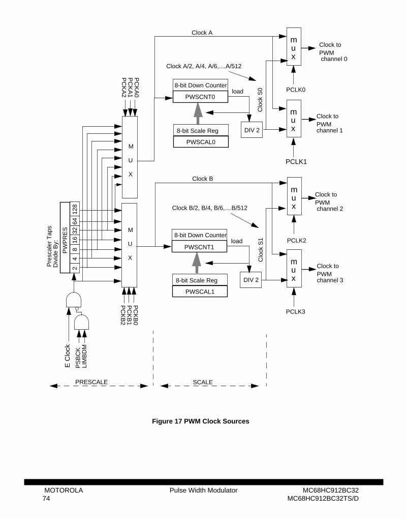
Figure 17 PWM Clock Sources
Clock B/2, B/4, B/6,....B/512
24
816
3264
128
PC
KB
2P
CK
B1
PC
KB
0
M
U
X
mux
PC
KA
2P
CK
A1
PC
KA
0
M
U
X
PCLK0
Clock toPWM
mux
PCLK1
Clock toPWM
loadPWSCNT0
DIV 28-bit Scale Reg
PWSCAL0
8-bit Down Counter
8-bit Down Counterload
PWSCNT1
DIV 28-bit Scale Reg
PWSCAL1
mux
PCLK2
Clock toPWM
mux
PCLK3
Clock toPWM
Clock A
Clock B
Clo
ck S
0C
lock
S1
Clock A/2, A/4, A/6,....A/512
PRESCALE SCALE
PW
PR
ES
Pre
scal
er T
aps
Div
ide
By:
PS
BC
KLI
MB
DM
E C
lock
channel 1
channel 0
channel 2
channel 3
MOTOROLA Pulse Width Modulator MC68HC912BC3274 MC68HC912BC32TS/D
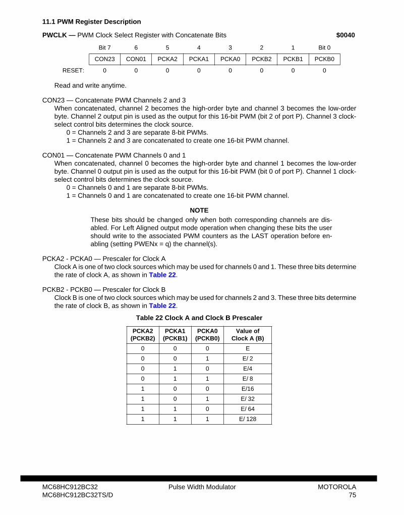
11.1 PWM Register Description
Read and write anytime.
CON23 — Concatenate PWM Channels 2 and 3When concatenated, channel 2 becomes the high-order byte and channel 3 becomes the low-orderbyte. Channel 2 output pin is used as the output for this 16-bit PWM (bit 2 of port P). Channel 3 clock-select control bits determines the clock source.
0 = Channels 2 and 3 are separate 8-bit PWMs. 1 = Channels 2 and 3 are concatenated to create one 16-bit PWM channel.
CON01 — Concatenate PWM Channels 0 and 1When concatenated, channel 0 becomes the high-order byte and channel 1 becomes the low-orderbyte. Channel 0 output pin is used as the output for this 16-bit PWM (bit 0 of port P). Channel 1 clock-select control bits determines the clock source.
0 = Channels 0 and 1 are separate 8-bit PWMs.1 = Channels 0 and 1 are concatenated to create one 16-bit PWM channel.
NOTEThese bits should be changed only when both corresponding channels are dis-abled. For Left Aligned output mode operation when changing these bits the usershould write to the associated PWM counters as the LAST operation before en-abling (setting PWENx = q) the channel(s).
PCKA2 - PCKA0 — Prescaler for Clock A Clock A is one of two clock sources which may be used for channels 0 and 1. These three bits determinethe rate of clock A, as shown in Table 22.
PCKB2 - PCKB0 — Prescaler for Clock B Clock B is one of two clock sources which may be used for channels 2 and 3. These three bits determinethe rate of clock B, as shown in Table 22.
PWCLK — PWM Clock Select Register with Concatenate Bits $0040
Bit 7 6 5 4 3 2 1 Bit 0
CON23 CON01 PCKA2 PCKA1 PCKA0 PCKB2 PCKB1 PCKB0
RESET: 0 0 0 0 0 0 0 0
Table 22 Clock A and Clock B Prescaler
PCKA2(PCKB2)
PCKA1(PCKB1)
PCKA0(PCKB0)
Value ofClock A (B)
0 0 0 E
0 0 1 E/ 2
0 1 0 E/4
0 1 1 E/ 8
1 0 0 E/16
1 0 1 E/ 32
1 1 0 E/ 64
1 1 1 E/ 128
MC68HC912BC32 Pulse Width Modulator MOTOROLAMC68HC912BC32TS/D 75
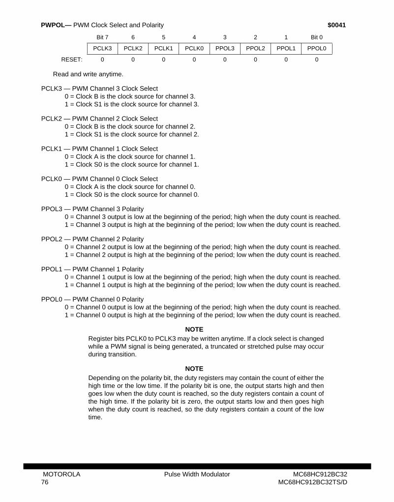
Read and write anytime.
PCLK3 — PWM Channel 3 Clock Select 0 = Clock B is the clock source for channel 3.1 = Clock S1 is the clock source for channel 3.
PCLK2 — PWM Channel 2 Clock Select 0 = Clock B is the clock source for channel 2. 1 = Clock S1 is the clock source for channel 2.
PCLK1 — PWM Channel 1 Clock Select 0 = Clock A is the clock source for channel 1.1 = Clock S0 is the clock source for channel 1.
PCLK0 — PWM Channel 0 Clock Select 0 = Clock A is the clock source for channel 0.1 = Clock S0 is the clock source for channel 0.
PPOL3 — PWM Channel 3 Polarity0 = Channel 3 output is low at the beginning of the period; high when the duty count is reached.1 = Channel 3 output is high at the beginning of the period; low when the duty count is reached.
PPOL2 — PWM Channel 2 Polarity0 = Channel 2 output is low at the beginning of the period; high when the duty count is reached.1 = Channel 2 output is high at the beginning of the period; low when the duty count is reached.
PPOL1 — PWM Channel 1 Polarity0 = Channel 1 output is low at the beginning of the period; high when the duty count is reached.1 = Channel 1 output is high at the beginning of the period; low when the duty count is reached.
PPOL0 — PWM Channel 0 Polarity0 = Channel 0 output is low at the beginning of the period; high when the duty count is reached.1 = Channel 0 output is high at the beginning of the period; low when the duty count is reached.
NOTERegister bits PCLK0 to PCLK3 may be written anytime. If a clock select is changedwhile a PWM signal is being generated, a truncated or stretched pulse may occurduring transition.
NOTEDepending on the polarity bit, the duty registers may contain the count of either thehigh time or the low time. If the polarity bit is one, the output starts high and thengoes low when the duty count is reached, so the duty registers contain a count ofthe high time. If the polarity bit is zero, the output starts low and then goes highwhen the duty count is reached, so the duty registers contain a count of the lowtime.
PWPOL— PWM Clock Select and Polarity $0041
Bit 7 6 5 4 3 2 1 Bit 0
PCLK3 PCLK2 PCLK1 PCLK0 PPOL3 PPOL2 PPOL1 PPOL0
RESET: 0 0 0 0 0 0 0 0
MOTOROLA Pulse Width Modulator MC68HC912BC3276 MC68HC912BC32TS/D
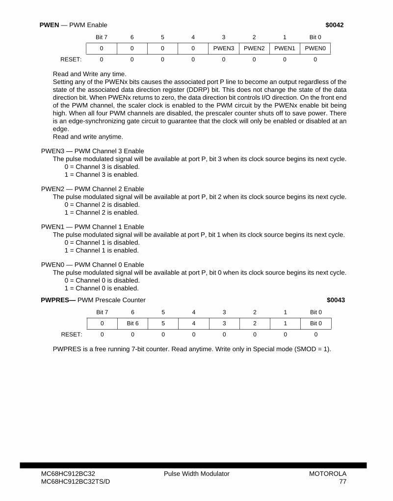
Read and Write any time.Setting any of the PWENx bits causes the associated port P line to become an output regardless of thestate of the associated data direction register (DDRP) bit. This does not change the state of the datadirection bit. When PWENx returns to zero, the data direction bit controls I/O direction. On the front endof the PWM channel, the scaler clock is enabled to the PWM circuit by the PWENx enable bit beinghigh. When all four PWM channels are disabled, the prescaler counter shuts off to save power. Thereis an edge-synchronizing gate circuit to guarantee that the clock will only be enabled or disabled at anedge.Read and write anytime.
PWEN3 — PWM Channel 3 Enable The pulse modulated signal will be available at port P, bit 3 when its clock source begins its next cycle.
0 = Channel 3 is disabled. 1 = Channel 3 is enabled.
PWEN2 — PWM Channel 2 Enable The pulse modulated signal will be available at port P, bit 2 when its clock source begins its next cycle.
0 = Channel 2 is disabled. 1 = Channel 2 is enabled.
PWEN1 — PWM Channel 1 Enable The pulse modulated signal will be available at port P, bit 1 when its clock source begins its next cycle.
0 = Channel 1 is disabled. 1 = Channel 1 is enabled.
PWEN0 — PWM Channel 0 Enable The pulse modulated signal will be available at port P, bit 0 when its clock source begins its next cycle.
0 = Channel 0 is disabled. 1 = Channel 0 is enabled.
PWPRES is a free running 7-bit counter. Read anytime. Write only in Special mode (SMOD = 1).
PWEN — PWM Enable $0042
Bit 7 6 5 4 3 2 1 Bit 0
0 0 0 0 PWEN3 PWEN2 PWEN1 PWEN0
RESET: 0 0 0 0 0 0 0 0
PWPRES— PWM Prescale Counter $0043
Bit 7 6 5 4 3 2 1 Bit 0
0 Bit 6 5 4 3 2 1 Bit 0
RESET: 0 0 0 0 0 0 0 0
MC68HC912BC32 Pulse Width Modulator MOTOROLAMC68HC912BC32TS/D 77
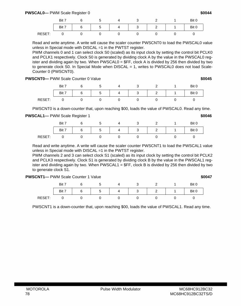
Read and write anytime. A write will cause the scaler counter PWSCNT0 to load the PWSCAL0 valueunless in Special mode with DISCAL =1 in the PWTST register.PWM channels 0 and 1 can select clock S0 (scaled) as its input clock by setting the control bit PCLK0and PCLK1 respectively. Clock S0 is generated by dividing clock A by the value in the PWSCAL0 reg-ister and dividing again by two. When PWSCAL0 = $FF, clock A is divided by 256 then divided by twoto generate clock S0. In Special Mode when DISCAL = 1, writes to PWSCAL0 does not load Scale-Counter 0 (PWSCNT0).
PWSCNT0 is a down-counter that, upon reaching $00, loads the value of PWSCAL0. Read any time.
Read and write anytime. A write will cause the scaler counter PWSCNT1 to load the PWSCAL1 valueunless in Special mode with DISCAL =1 in the PWTST register.PWM channels 2 and 3 can select clock S1 (scaled) as its input clock by setting the control bit PCLK2and PCLK3 respectively. Clock S1 is generated by dividing clock B by the value in the PWSCAL1 reg-ister and dividing again by two. When PWSCAL1 = $FF, clock B is divided by 256 then divided by twoto generate clock S1.
PWSCNT1 is a down-counter that, upon reaching $00, loads the value of PWSCAL1. Read any time.
PWSCAL0— PWM Scale Register 0 $0044
Bit 7 6 5 4 3 2 1 Bit 0
Bit 7 6 5 4 3 2 1 Bit 0
RESET: 0 0 0 0 0 0 0 0
PWSCNT0— PWM Scale Counter 0 Value $0045
Bit 7 6 5 4 3 2 1 Bit 0
Bit 7 6 5 4 3 2 1 Bit 0
RESET: 0 0 0 0 0 0 0 0
PWSCAL1— PWM Scale Register 1 $0046
Bit 7 6 5 4 3 2 1 Bit 0
Bit 7 6 5 4 3 2 1 Bit 0
RESET: 0 0 0 0 0 0 0 0
PWSCNT1— PWM Scale Counter 1 Value $0047
Bit 7 6 5 4 3 2 1 Bit 0
Bit 7 6 5 4 3 2 1 Bit 0
RESET: 0 0 0 0 0 0 0 0
MOTOROLA Pulse Width Modulator MC68HC912BC3278 MC68HC912BC32TS/D
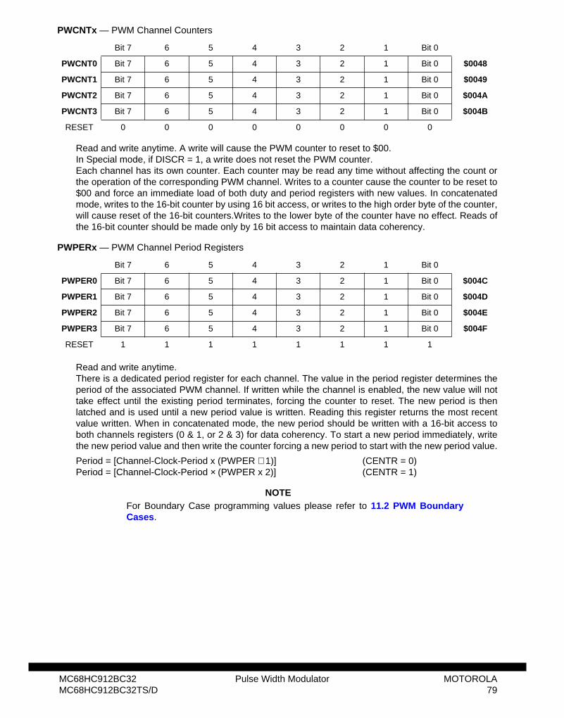
Read and write anytime. A write will cause the PWM counter to reset to $00. In Special mode, if DISCR = 1, a write does not reset the PWM counter.Each channel has its own counter. Each counter may be read any time without affecting the count orthe operation of the corresponding PWM channel. Writes to a counter cause the counter to be reset to$00 and force an immediate load of both duty and period registers with new values. In concatenatedmode, writes to the 16-bit counter by using 16 bit access, or writes to the high order byte of the counter,will cause reset of the 16-bit counters.Writes to the lower byte of the counter have no effect. Reads ofthe 16-bit counter should be made only by 16 bit access to maintain data coherency.
Read and write anytime.There is a dedicated period register for each channel. The value in the period register determines theperiod of the associated PWM channel. If written while the channel is enabled, the new value will nottake effect until the existing period terminates, forcing the counter to reset. The new period is thenlatched and is used until a new period value is written. Reading this register returns the most recentvalue written. When in concatenated mode, the new period should be written with a 16-bit access toboth channels registers (0 & 1, or 2 & 3) for data coherency. To start a new period immediately, writethe new period value and then write the counter forcing a new period to start with the new period value.
Period = [Channel-Clock-Period x (PWPER + 1)] (CENTR = 0)Period = [Channel-Clock-Period × (PWPER x 2)] (CENTR = 1)
NOTEFor Boundary Case programming values please refer to 11.2 PWM BoundaryCases.
PWCNTx — PWM Channel Counters
Bit 7 6 5 4 3 2 1 Bit 0
PWCNT0 Bit 7 6 5 4 3 2 1 Bit 0 $0048
PWCNT1 Bit 7 6 5 4 3 2 1 Bit 0 $0049
PWCNT2 Bit 7 6 5 4 3 2 1 Bit 0 $004A
PWCNT3 Bit 7 6 5 4 3 2 1 Bit 0 $004B
RESET 0 0 0 0 0 0 0 0
PWPERx — PWM Channel Period Registers
Bit 7 6 5 4 3 2 1 Bit 0
PWPER0 Bit 7 6 5 4 3 2 1 Bit 0 $004C
PWPER1 Bit 7 6 5 4 3 2 1 Bit 0 $004D
PWPER2 Bit 7 6 5 4 3 2 1 Bit 0 $004E
PWPER3 Bit 7 6 5 4 3 2 1 Bit 0 $004F
RESET 1 1 1 1 1 1 1 1
MC68HC912BC32 Pulse Width Modulator MOTOROLAMC68HC912BC32TS/D 79
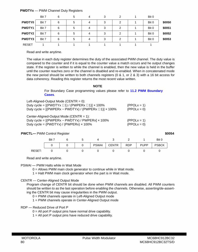
Read and write anytime.
The value in each duty register determines the duty of the associated PWM channel. The duty value iscompared to the counter and if it is equal to the counter value a match occurs and he output changesstate. If the register is written to while the channel is enabled, then the new value is held in the bufferuntil the counter reaches zero or the channel is disabled and re-enabled. When in concatenated modethe new period should be written to both channels registers (0 & 1, or 2 & 3) with a 16 bit access fordata coherency. Reading this register returns the most recent value written.
NOTEFor Boundary Case programming values please refer to 11.2 PWM BoundaryCases.
Left-Aligned-Output Mode (CENTR = 0):Duty cycle = [(PWDTYx + 1) / (PWPERx + 1)] × 100% (PPOLx = 1)Duty cycle = [(PWPERx − PWDTYx) / (PWPERx + 1)] × 100% (PPOLx = 0)
Center-Aligned-Output Mode (CENTR = 1):Duty cycle = [(PWPERx − PWDTYx) / PWPERx] × 100% (PPOLx = 1)Duty cycle = (PWDTYx) / (PWPERx) × 100% (PPOLx = 0)
Read and write anytime.
PSWAI — PWM Halts while in Wait Mode0 = Allows PWM main clock generator to continue while in Wait mode.1 = Halt PWM main clock generator when the part is in Wait mode.
CENTR — Center-Aligned Output ModeProgram change of CENTR bit should be done when PWM channels are disabled. All PWM countersshould be written to as the last operation before enabling the channels. Otherwise, asserting/de-assert-ing the CENTR bit may cause irregularities in the PWM output.
0 = PWM channels operate in Left-Aligned Output mode1 = PWM channels operate in Center-Aligned Output mode
RDP — Reduced Drive of Port P0 = All port P output pins have normal drive capability.1 = All port P output pins have reduced drive capability.
PWDTYx — PWM Channel Duty Registers
Bit 7 6 5 4 3 2 1 Bit 0
PWDTY0 Bit 7 6 5 4 3 2 1 Bit 0 $0050
PWDTY1 Bit 7 6 5 4 3 2 1 Bit 0 $0051
PWDTY2 Bit 7 6 5 4 3 2 1 Bit 0 $0052
PWDTY3 Bit 7 6 5 4 3 2 1 Bit 0 $0053
RESET 1 1 1 1 1 1 1 1
PWCTL— PWM Control Register $0054
Bit 7 6 5 4 3 2 1 Bit 0
0 0 0 PSWAI CENTR RDP PUPP PSBCK
RESET: 0 0 0 0 0 0 0 0
MOTOROLA Pulse Width Modulator MC68HC912BC3280 MC68HC912BC32TS/D
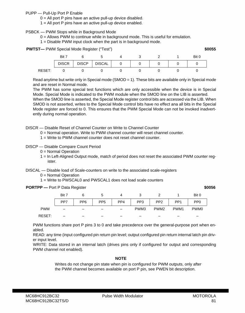
PUPP — Pull-Up Port P Enable0 = All port P pins have an active pull-up device disabled.1 = All port P pins have an active pull-up device enabled.
PSBCK — PWM Stops while in Background Mode0 = Allows PWM to continue while in background mode. This is useful for emulation.1 = Disable PWM input clock when the part is in background mode.
Read anytime but write only in Special mode (SMOD = 1). These bits are available only in Special modeand are reset in Normal mode.The PWM has some special test functions which are only accessible when the device is in SpecialMode. Special Mode is indicated to the PWM module when the SMOD line on the LIB is asserted.When the SMOD line is asserted, the Special Mode register control bits are accessed via the LIB. WhenSMOD is not asserted, writes to the Special Mode control bits have no effect ana all bits in the SpecialMode register are forced to 0. This ensures that the PWM Special Mode can not be invoked inadvert-ently during normal operation.
DISCR — Disable Reset of Channel Counter on Write to Channel Counter0 = Normal operation. Write to PWM channel counter will reset channel counter.1 = Write to PWM channel counter does not reset channel counter.
DISCP — Disable Compare Count Period0 = Normal Operation1 = In Left-Aligned Output mode, match of period does not reset the associated PWM counter reg-
ister.
DISCAL — Disable load of Scale-counters on write to the associated scale-registers0 = Normal Operation1 = Write to PWSCAL0 and PWSCAL1 does not load scale counters
PWM functions share port P pins 3 to 0 and take precedence over the general-purpose port when en-abled. READ: any time (input configured pin return pin level; output configured pin return internal latch pin driv-er input level.WRITE: Data stored in an internal latch (drives pins only if configured for output and correspondingPWM channel not enabled).
NOTEWrites do not change pin state when pin is configured for PWM outputs, only afterthe PWM channel becomes available on port P pin, see PWEN bit description.
PWTST— PWM Special Mode Register (“Test”) $0055
Bit 7 6 5 4 3 2 1 Bit 0
DISCR DISCP DISCAL 0 0 0 0 0
RESET: 0 0 0 0 0 0 0 0
PORTPP — Port P Data Register $0056
Bit 7 6 5 4 3 2 1 Bit 0
PP7 PP6 PP5 PP4 PP3 PP2 PP1 PP0
PWM – – – – PWM3 PWM2 PWM1 PWM0
RESET: – – – – – – – –
MC68HC912BC32 Pulse Width Modulator MOTOROLAMC68HC912BC32TS/D 81
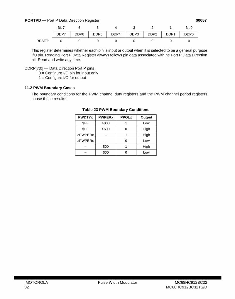
.
This register determines whether each pin is input or output when it is selected to be a general purposeI/O pin. Reading Port P Data Register always follows pin data associated with he Port P Data Directionbit. Read and write any time.
DDRP[7:0] — Data Direction Port P pins0 = Configure I/O pin for input only1 = Configure I/O for output
11.2 PWM Boundary Cases
The boundary conditions for the PWM channel duty registers and the PWM channel period registerscause these results:
PORTPD — Port P Data Direction Register $0057
Bit 7 6 5 4 3 2 1 Bit 0
DDP7 DDP6 DDP5 DDP4 DDP3 DDP2 DDP1 DDP0
RESET: 0 0 0 0 0 0 0 0
Table 23 PWM Boundary Conditions
PWDTYx PWPERx PPOLx Output
$FF >$00 1 Low
$FF >$00 0 High
≥PWPERx – 1 High
≥PWPERx – 0 Low
– $00 1 High
– $00 0 Low
MOTOROLA Pulse Width Modulator MC68HC912BC3282 MC68HC912BC32TS/D
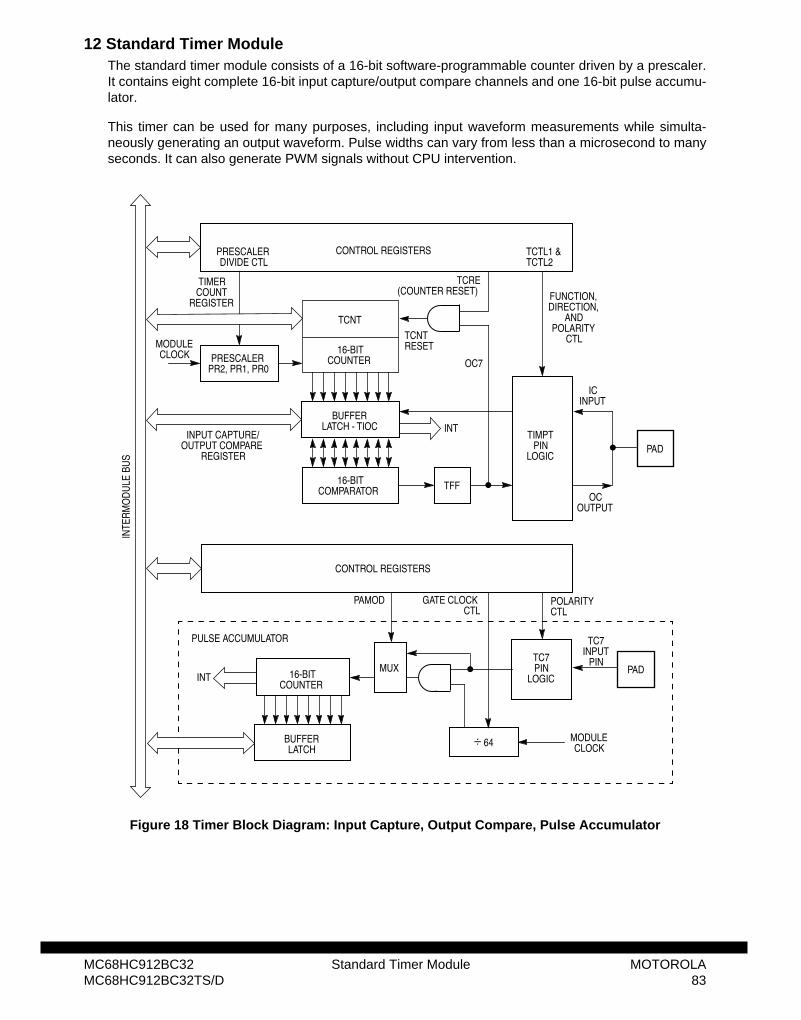
12 Standard Timer ModuleThe standard timer module consists of a 16-bit software-programmable counter driven by a prescaler.It contains eight complete 16-bit input capture/output compare channels and one 16-bit pulse accumu-lator.
This timer can be used for many purposes, including input waveform measurements while simulta-neously generating an output waveform. Pulse widths can vary from less than a microsecond to manyseconds. It can also generate PWM signals without CPU intervention.
Figure 18 Timer Block Diagram: Input Capture, Output Compare, Pulse Accumulator
TFF
PAD
INT
OC7
PADINT
MUX
PAMOD
PULSE ACCUMULATOR
CONTROL REGISTERS
÷ 64
TC7PIN
LOGIC
MODULECLOCK
16-BITCOUNTER
BUFFERLATCH
TC7INPUT
PIN
POLARITYCTL
GATE CLOCKCTL
TIMPTPIN
LOGIC
FUNCTION,DIRECTION,
ANDPOLARITY
CTL
CONTROL REGISTERSPRESCALERDIVIDE CTL
TCTL1 &TCTL2
INPUT CAPTURE/OUTPUT COMPARE
REGISTER
16-BITCOMPARATOR
INTE
RM
OD
ULE
BU
S
OCOUTPUT
ICINPUT
BUFFERLATCH - TIOC
TCRE(COUNTER RESET)
TCNTRESET
TCNT
16-BITCOUNTERPRESCALER
PR2, PR1, PR0
TIMERCOUNT
REGISTER
MODULECLOCK
MC68HC912BC32 Standard Timer Module MOTOROLAMC68HC912BC32TS/D 83
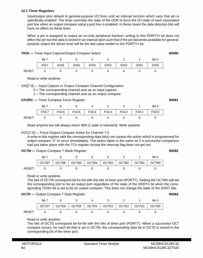
12.1 Timer Registers
Input/output pins default to general-purpose I/O lines until an internal function which uses that pin isspecifically enabled. The timer overrides the state of the DDR to force the I/O state of each associatedport line when an output compare using a port line is enabled. In these cases the data direction bits willhave no affect on these lines.
When a pin is assigned to output an on-chip peripheral function, writing to this PORTTn bit does notaffect the pin but the data is stored in an internal latch such that if the pin becomes available for general-purpose output the driven level will be the last value written to the PORTTn bit.
Read or write anytime.
IOS[7:0] — Input Capture or Output Compare Channel Configuration0 = The corresponding channel acts as an input capture1 = The corresponding channel acts as an output compare.
Read anytime but will always return $00 (1 state is transient). Write anytime.
FOC[7:0] — Force Output Compare Action for Channel 7-0 A write to this register with the corresponding data bit(s) set causes the action which is programmed foroutput compare “n” to occur immediately. The action taken is the same as if a successful comparisonhad just taken place with the TCn register except the interrupt flag does not get set.
Read or write anytime.The bits of OC7M correspond bit-for-bit with the bits of timer port (PORTT). Setting the OC7Mn will setthe corresponding port to be an output port regardless of the state of the DDRTn bit when the corre-sponding TIOSn bit is set to be an output compare. This does not change the state of the DDRT bits.
Read or write anytime.The bits of OC7D correspond bit-for-bit with the bits of timer port (PORTT). When a successful OC7
TIOS — Timer Input Capture/Output Compare Select $0080
Bit 7 6 5 4 3 2 1 Bit 0
IOS7 IOS6 IOS5 IOS4 IOS3 IOS2 IOS1 IOS0
RESET: 0 0 0 0 0 0 0 0
CFORC — Timer Compare Force Register $0081
Bit 7 6 5 4 3 2 1 Bit 0
FOC7 FOC6 FOC5 FOC4 FOC3 FOC2 FOC1 FOC0
RESET: 0 0 0 0 0 0 0 0
OC7M — Output Compare 7 Mask Register $0082
Bit 7 6 5 4 3 2 1 Bit 0
OC7M7 OC7M6 OC7M5 OC7M4 OC7M3 OC7M2 OC7M1 OC7M0
RESET: 0 0 0 0 0 0 0 0
OC7D — Output Compare 7 Data Register $0083
Bit 7 6 5 4 3 2 1 Bit 0
OC7D7 OC7D6 OC7D5 OC7D4 OC7D3 OC7D2 OC7D1 OC7D0
RESET: 0 0 0 0 0 0 0 0
MOTOROLA Standard Timer Module MC68HC912BC3284 MC68HC912BC32TS/D
compare occurs, for each bit that is set in OC7M, the corresponding data bit in OC7D is stored to thecorresponding bit of the timer port.
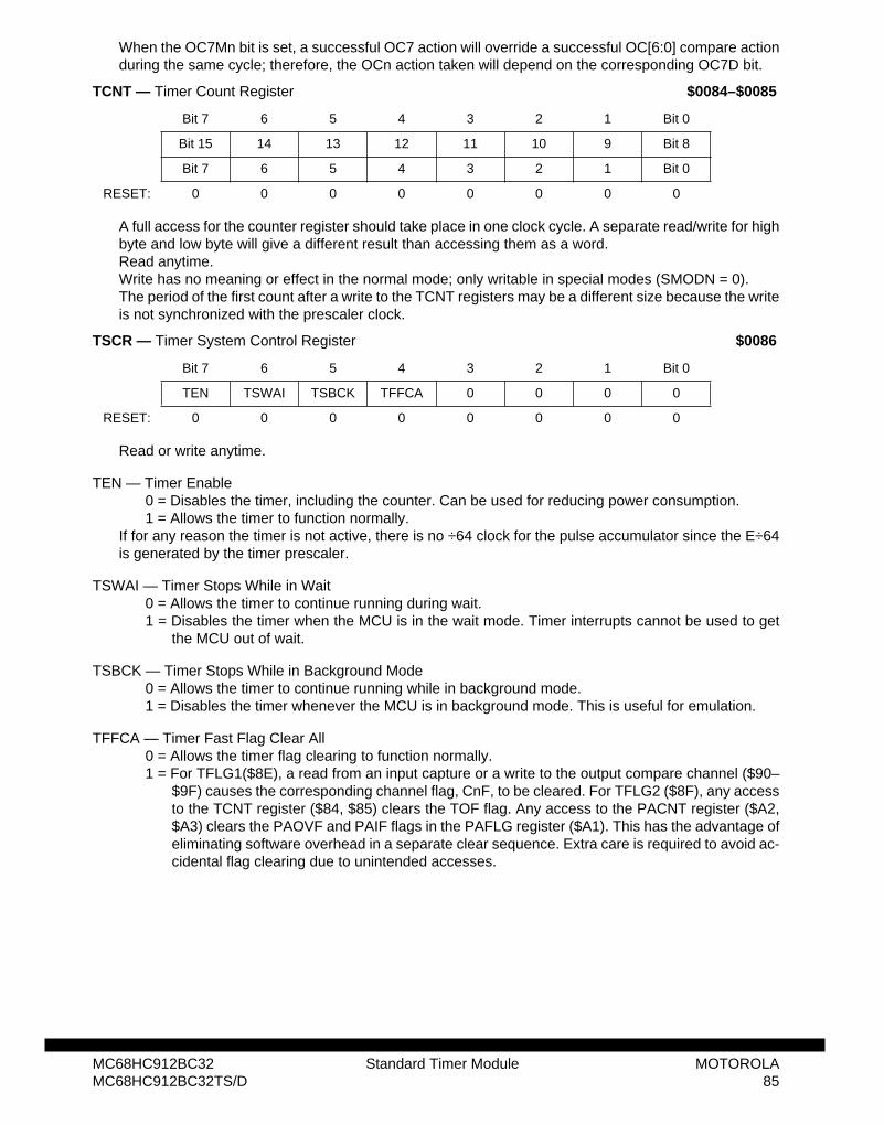
When the OC7Mn bit is set, a successful OC7 action will override a successful OC[6:0] compare actionduring the same cycle; therefore, the OCn action taken will depend on the corresponding OC7D bit.
A full access for the counter register should take place in one clock cycle. A separate read/write for highbyte and low byte will give a different result than accessing them as a word.Read anytime.Write has no meaning or effect in the normal mode; only writable in special modes (SMODN = 0).The period of the first count after a write to the TCNT registers may be a different size because the writeis not synchronized with the prescaler clock.
Read or write anytime.
TEN — Timer Enable0 = Disables the timer, including the counter. Can be used for reducing power consumption.1 = Allows the timer to function normally.
If for any reason the timer is not active, there is no ÷64 clock for the pulse accumulator since the E÷64is generated by the timer prescaler.
TSWAI — Timer Stops While in Wait0 = Allows the timer to continue running during wait.1 = Disables the timer when the MCU is in the wait mode. Timer interrupts cannot be used to get
the MCU out of wait.
TSBCK — Timer Stops While in Background Mode0 = Allows the timer to continue running while in background mode.1 = Disables the timer whenever the MCU is in background mode. This is useful for emulation.
TFFCA — Timer Fast Flag Clear All 0 = Allows the timer flag clearing to function normally.1 = For TFLG1($8E), a read from an input capture or a write to the output compare channel ($90–
$9F) causes the corresponding channel flag, CnF, to be cleared. For TFLG2 ($8F), any accessto the TCNT register ($84, $85) clears the TOF flag. Any access to the PACNT register ($A2,$A3) clears the PAOVF and PAIF flags in the PAFLG register ($A1). This has the advantage ofeliminating software overhead in a separate clear sequence. Extra care is required to avoid ac-cidental flag clearing due to unintended accesses.
TCNT — Timer Count Register $0084–$0085
Bit 7 6 5 4 3 2 1 Bit 0
Bit 15 14 13 12 11 10 9 Bit 8
Bit 7 6 5 4 3 2 1 Bit 0
RESET: 0 0 0 0 0 0 0 0
TSCR — Timer System Control Register $0086
Bit 7 6 5 4 3 2 1 Bit 0
TEN TSWAI TSBCK TFFCA 0 0 0 0
RESET: 0 0 0 0 0 0 0 0
MC68HC912BC32 Standard Timer Module MOTOROLAMC68HC912BC32TS/D 85
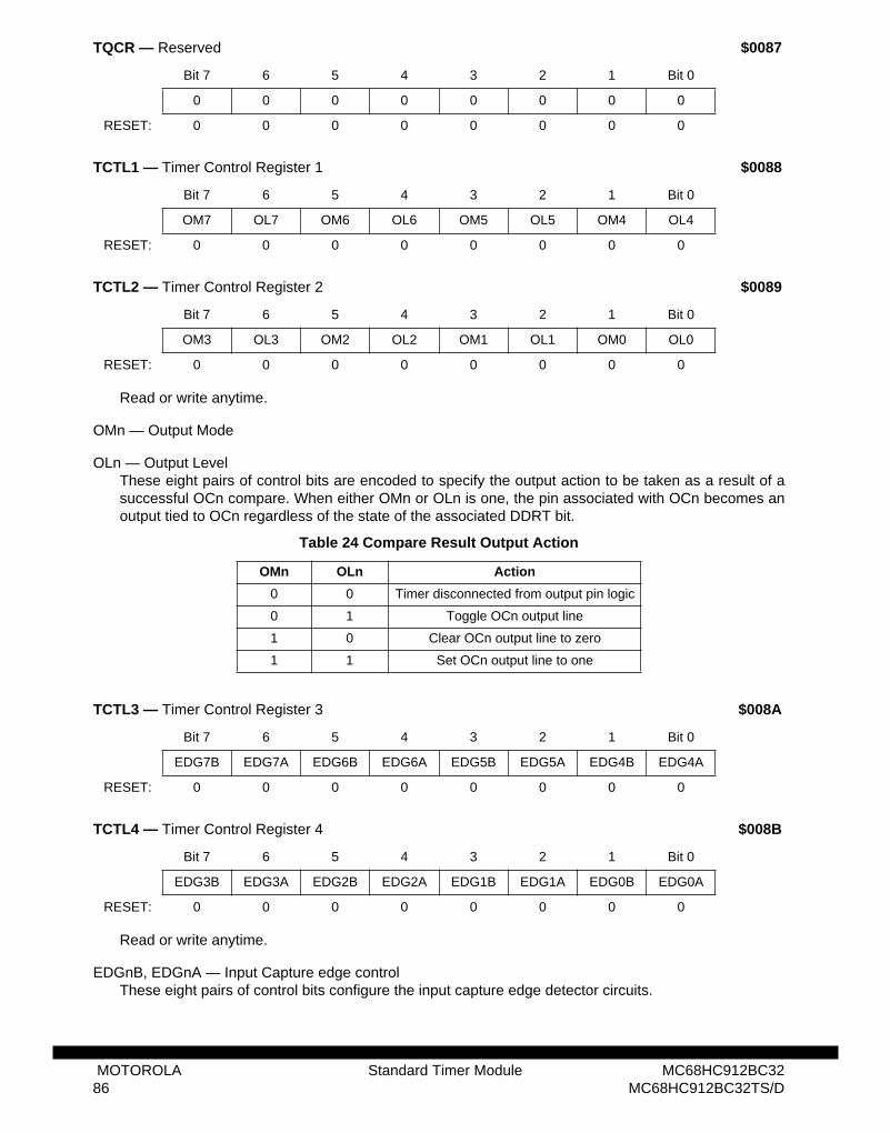
Read or write anytime.
OMn — Output Mode
OLn — Output Level These eight pairs of control bits are encoded to specify the output action to be taken as a result of asuccessful OCn compare. When either OMn or OLn is one, the pin associated with OCn becomes anoutput tied to OCn regardless of the state of the associated DDRT bit.
Read or write anytime.
EDGnB, EDGnA — Input Capture edge control These eight pairs of control bits configure the input capture edge detector circuits.
TQCR — Reserved $0087
Bit 7 6 5 4 3 2 1 Bit 0
0 0 0 0 0 0 0 0
RESET: 0 0 0 0 0 0 0 0
TCTL1 — Timer Control Register 1 $0088
Bit 7 6 5 4 3 2 1 Bit 0
OM7 OL7 OM6 OL6 OM5 OL5 OM4 OL4
RESET: 0 0 0 0 0 0 0 0
TCTL2 — Timer Control Register 2 $0089
Bit 7 6 5 4 3 2 1 Bit 0
OM3 OL3 OM2 OL2 OM1 OL1 OM0 OL0
RESET: 0 0 0 0 0 0 0 0
Table 24 Compare Result Output Action
OMn OLn Action
0 0 Timer disconnected from output pin logic
0 1 Toggle OCn output line
1 0 Clear OCn output line to zero
1 1 Set OCn output line to one
TCTL3 — Timer Control Register 3 $008A
Bit 7 6 5 4 3 2 1 Bit 0
EDG7B EDG7A EDG6B EDG6A EDG5B EDG5A EDG4B EDG4A
RESET: 0 0 0 0 0 0 0 0
TCTL4 — Timer Control Register 4 $008B
Bit 7 6 5 4 3 2 1 Bit 0
EDG3B EDG3A EDG2B EDG2A EDG1B EDG1A EDG0B EDG0A
RESET: 0 0 0 0 0 0 0 0
MOTOROLA Standard Timer Module MC68HC912BC3286 MC68HC912BC32TS/D
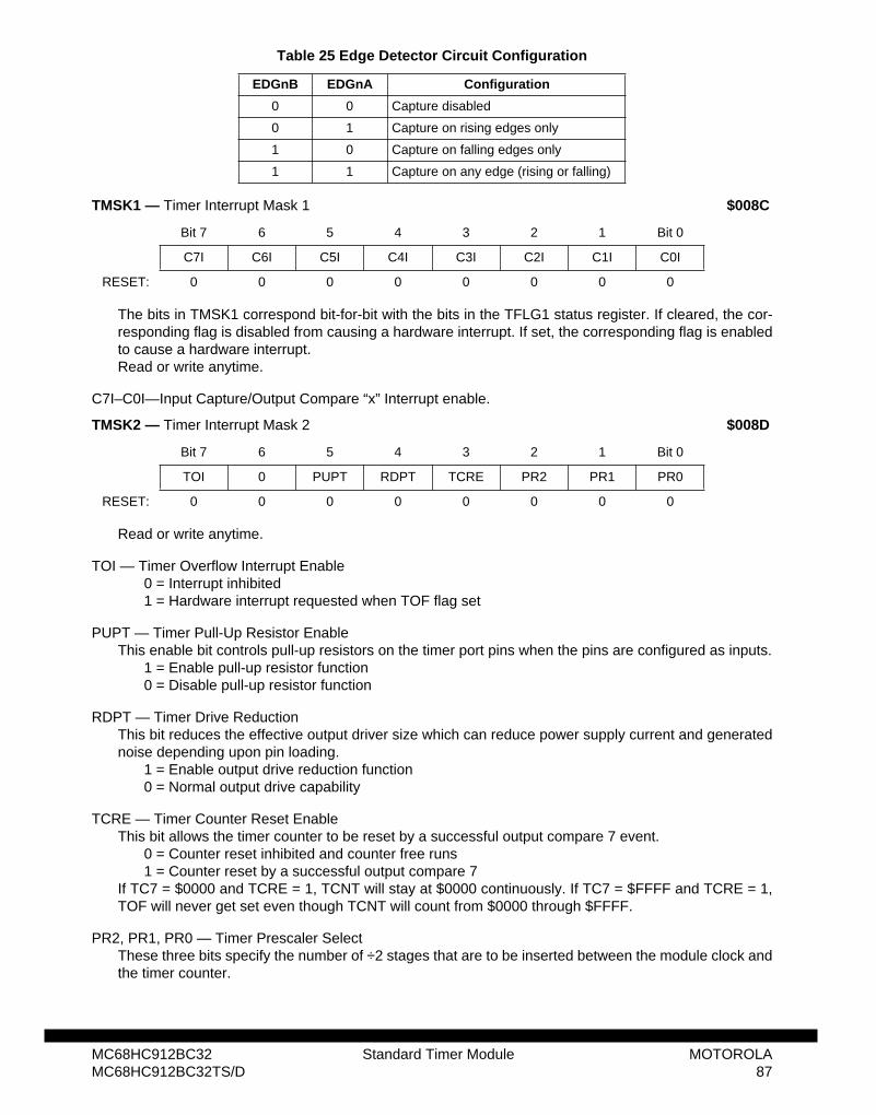
The bits in TMSK1 correspond bit-for-bit with the bits in the TFLG1 status register. If cleared, the cor-responding flag is disabled from causing a hardware interrupt. If set, the corresponding flag is enabledto cause a hardware interrupt. Read or write anytime.
C7I–C0I—Input Capture/Output Compare “x” Interrupt enable.
Read or write anytime.
TOI — Timer Overflow Interrupt Enable 0 = Interrupt inhibited 1 = Hardware interrupt requested when TOF flag set
PUPT — Timer Pull-Up Resistor EnableThis enable bit controls pull-up resistors on the timer port pins when the pins are configured as inputs.
1 = Enable pull-up resistor function0 = Disable pull-up resistor function
RDPT — Timer Drive ReductionThis bit reduces the effective output driver size which can reduce power supply current and generatednoise depending upon pin loading.
1 = Enable output drive reduction function0 = Normal output drive capability
TCRE — Timer Counter Reset Enable This bit allows the timer counter to be reset by a successful output compare 7 event.
0 = Counter reset inhibited and counter free runs1 = Counter reset by a successful output compare 7
If TC7 = $0000 and TCRE = 1, TCNT will stay at $0000 continuously. If TC7 = $FFFF and TCRE = 1,TOF will never get set even though TCNT will count from $0000 through $FFFF.
PR2, PR1, PR0 — Timer Prescaler Select These three bits specify the number of ÷2 stages that are to be inserted between the module clock andthe timer counter.
Table 25 Edge Detector Circuit Configuration
EDGnB EDGnA Configuration
0 0 Capture disabled
0 1 Capture on rising edges only
1 0 Capture on falling edges only
1 1 Capture on any edge (rising or falling)
TMSK1 — Timer Interrupt Mask 1 $008C
Bit 7 6 5 4 3 2 1 Bit 0
C7I C6I C5I C4I C3I C2I C1I C0I
RESET: 0 0 0 0 0 0 0 0
TMSK2 — Timer Interrupt Mask 2 $008D
Bit 7 6 5 4 3 2 1 Bit 0
TOI 0 PUPT RDPT TCRE PR2 PR1 PR0
RESET: 0 0 0 0 0 0 0 0
MC68HC912BC32 Standard Timer Module MOTOROLAMC68HC912BC32TS/D 87
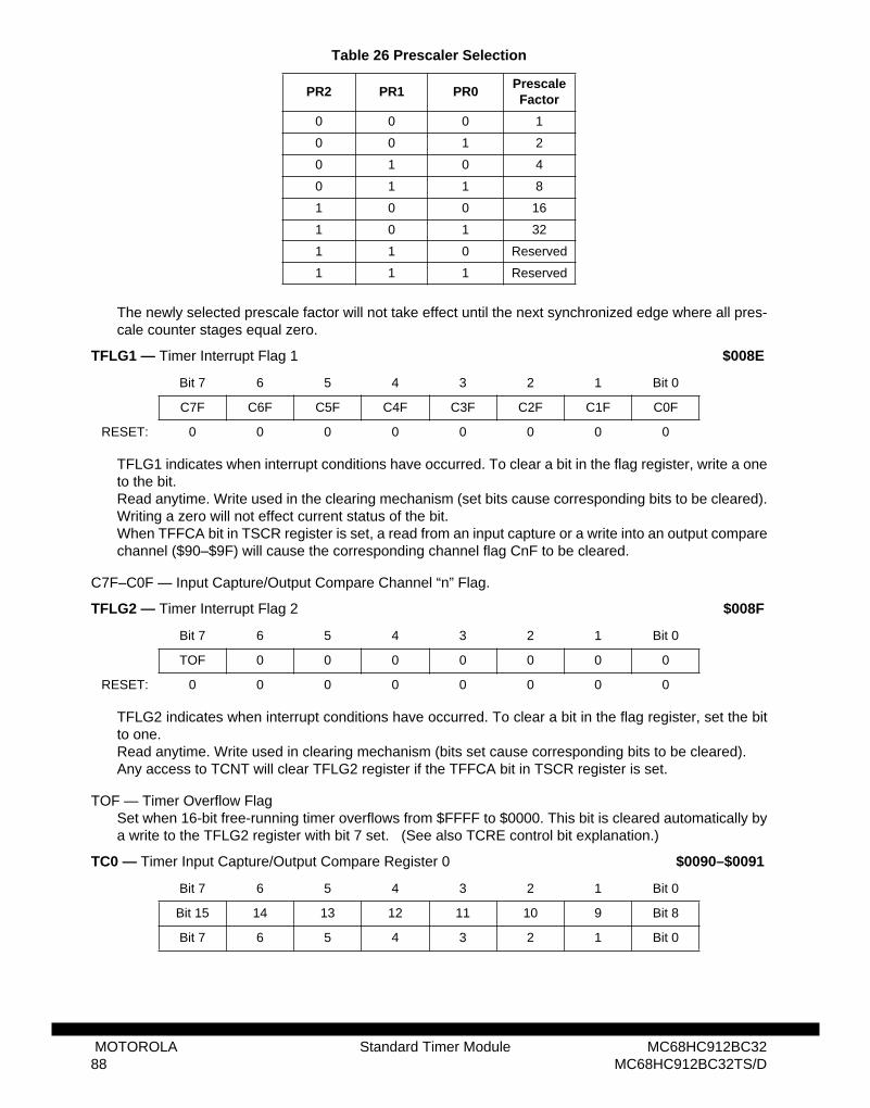
The newly selected prescale factor will not take effect until the next synchronized edge where all pres-cale counter stages equal zero.
TFLG1 indicates when interrupt conditions have occurred. To clear a bit in the flag register, write a oneto the bit.Read anytime. Write used in the clearing mechanism (set bits cause corresponding bits to be cleared).Writing a zero will not effect current status of the bit.When TFFCA bit in TSCR register is set, a read from an input capture or a write into an output comparechannel ($90–$9F) will cause the corresponding channel flag CnF to be cleared.
C7F–C0F — Input Capture/Output Compare Channel “n” Flag.
TFLG2 indicates when interrupt conditions have occurred. To clear a bit in the flag register, set the bitto one.Read anytime. Write used in clearing mechanism (bits set cause corresponding bits to be cleared).Any access to TCNT will clear TFLG2 register if the TFFCA bit in TSCR register is set.
TOF — Timer Overflow Flag Set when 16-bit free-running timer overflows from $FFFF to $0000. This bit is cleared automatically bya write to the TFLG2 register with bit 7 set. (See also TCRE control bit explanation.)
Table 26 Prescaler Selection
PR2 PR1 PR0Prescale Factor
0 0 0 1
0 0 1 2
0 1 0 4
0 1 1 8
1 0 0 16
1 0 1 32
1 1 0 Reserved
1 1 1 Reserved
TFLG1 — Timer Interrupt Flag 1 $008E
Bit 7 6 5 4 3 2 1 Bit 0
C7F C6F C5F C4F C3F C2F C1F C0F
RESET: 0 0 0 0 0 0 0 0
TFLG2 — Timer Interrupt Flag 2 $008F
Bit 7 6 5 4 3 2 1 Bit 0
TOF 0 0 0 0 0 0 0
RESET: 0 0 0 0 0 0 0 0
TC0 — Timer Input Capture/Output Compare Register 0 $0090–$0091
Bit 7 6 5 4 3 2 1 Bit 0
Bit 15 14 13 12 11 10 9 Bit 8
Bit 7 6 5 4 3 2 1 Bit 0
MOTOROLA Standard Timer Module MC68HC912BC3288 MC68HC912BC32TS/D
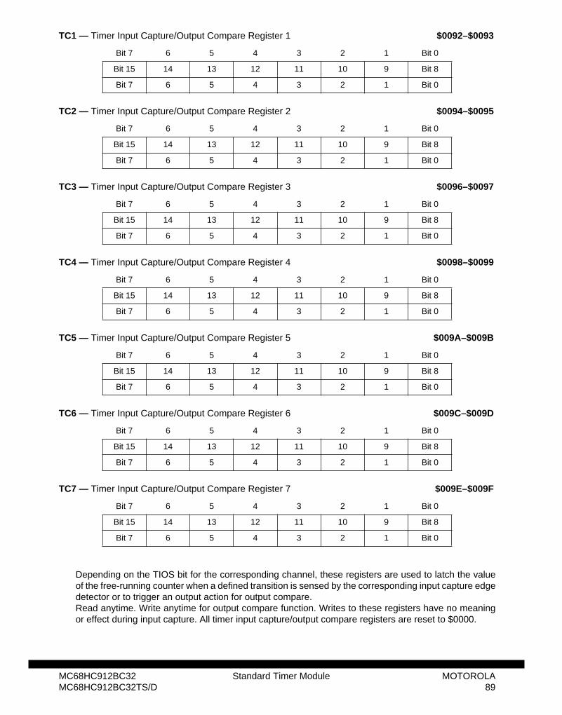
Depending on the TIOS bit for the corresponding channel, these registers are used to latch the valueof the free-running counter when a defined transition is sensed by the corresponding input capture edgedetector or to trigger an output action for output compare. Read anytime. Write anytime for output compare function. Writes to these registers have no meaningor effect during input capture. All timer input capture/output compare registers are reset to $0000.
TC1 — Timer Input Capture/Output Compare Register 1 $0092–$0093
Bit 7 6 5 4 3 2 1 Bit 0
Bit 15 14 13 12 11 10 9 Bit 8
Bit 7 6 5 4 3 2 1 Bit 0
TC2 — Timer Input Capture/Output Compare Register 2 $0094–$0095
Bit 7 6 5 4 3 2 1 Bit 0
Bit 15 14 13 12 11 10 9 Bit 8
Bit 7 6 5 4 3 2 1 Bit 0
TC3 — Timer Input Capture/Output Compare Register 3 $0096–$0097
Bit 7 6 5 4 3 2 1 Bit 0
Bit 15 14 13 12 11 10 9 Bit 8
Bit 7 6 5 4 3 2 1 Bit 0
TC4 — Timer Input Capture/Output Compare Register 4 $0098–$0099
Bit 7 6 5 4 3 2 1 Bit 0
Bit 15 14 13 12 11 10 9 Bit 8
Bit 7 6 5 4 3 2 1 Bit 0
TC5 — Timer Input Capture/Output Compare Register 5 $009A–$009B
Bit 7 6 5 4 3 2 1 Bit 0
Bit 15 14 13 12 11 10 9 Bit 8
Bit 7 6 5 4 3 2 1 Bit 0
TC6 — Timer Input Capture/Output Compare Register 6 $009C–$009D
Bit 7 6 5 4 3 2 1 Bit 0
Bit 15 14 13 12 11 10 9 Bit 8
Bit 7 6 5 4 3 2 1 Bit 0
TC7 — Timer Input Capture/Output Compare Register 7 $009E–$009F
Bit 7 6 5 4 3 2 1 Bit 0
Bit 15 14 13 12 11 10 9 Bit 8
Bit 7 6 5 4 3 2 1 Bit 0
MC68HC912BC32 Standard Timer Module MOTOROLAMC68HC912BC32TS/D 89
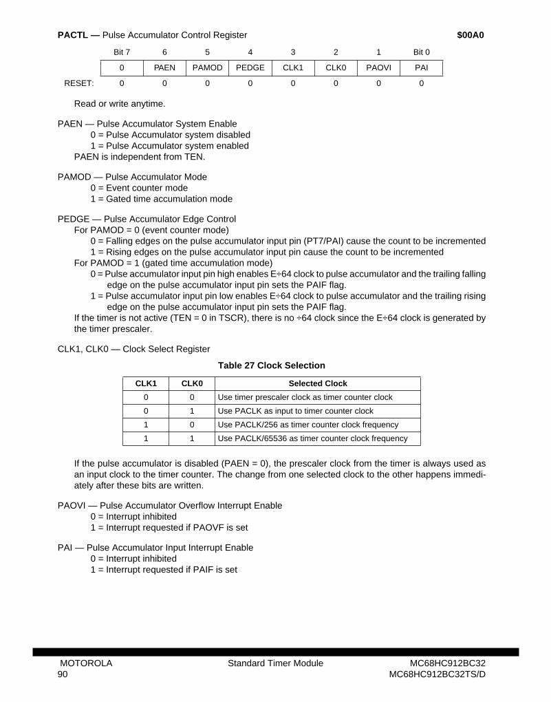
Read or write anytime.
PAEN — Pulse Accumulator System Enable 0 = Pulse Accumulator system disabled1 = Pulse Accumulator system enabled
PAEN is independent from TEN.
PAMOD — Pulse Accumulator Mode 0 = Event counter mode 1 = Gated time accumulation mode
PEDGE — Pulse Accumulator Edge Control For PAMOD = 0 (event counter mode)
0 = Falling edges on the pulse accumulator input pin (PT7/PAI) cause the count to be incremented1 = Rising edges on the pulse accumulator input pin cause the count to be incremented
For PAMOD = 1 (gated time accumulation mode)0 = Pulse accumulator input pin high enables E÷64 clock to pulse accumulator and the trailing falling
edge on the pulse accumulator input pin sets the PAIF flag. 1 = Pulse accumulator input pin low enables E÷64 clock to pulse accumulator and the trailing rising
edge on the pulse accumulator input pin sets the PAIF flag. If the timer is not active (TEN = 0 in TSCR), there is no ÷64 clock since the E÷64 clock is generated bythe timer prescaler.
CLK1, CLK0 — Clock Select Register
If the pulse accumulator is disabled (PAEN = 0), the prescaler clock from the timer is always used asan input clock to the timer counter. The change from one selected clock to the other happens immedi-ately after these bits are written.
PAOVI — Pulse Accumulator Overflow Interrupt Enable0 = Interrupt inhibited1 = Interrupt requested if PAOVF is set
PAI — Pulse Accumulator Input Interrupt Enable0 = Interrupt inhibited 1 = Interrupt requested if PAIF is set
PACTL — Pulse Accumulator Control Register $00A0
Bit 7 6 5 4 3 2 1 Bit 0
0 PAEN PAMOD PEDGE CLK1 CLK0 PAOVI PAI
RESET: 0 0 0 0 0 0 0 0
Table 27 Clock Selection
CLK1 CLK0 Selected Clock
0 0 Use timer prescaler clock as timer counter clock
0 1 Use PACLK as input to timer counter clock
1 0 Use PACLK/256 as timer counter clock frequency
1 1 Use PACLK/65536 as timer counter clock frequency
MOTOROLA Standard Timer Module MC68HC912BC3290 MC68HC912BC32TS/D
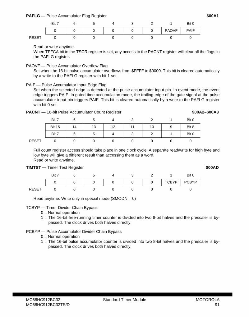
Read or write anytime.When TFFCA bit in the TSCR register is set, any access to the PACNT register will clear all the flags inthe PAFLG register.
PAOVF — Pulse Accumulator Overflow FlagSet when the 16-bit pulse accumulator overflows from $FFFF to $0000. This bit is cleared automaticallyby a write to the PAFLG register with bit 1 set.
PAIF — Pulse Accumulator Input Edge FlagSet when the selected edge is detected at the pulse accumulator input pin. In event mode, the eventedge triggers PAIF. In gated time accumulation mode, the trailing edge of the gate signal at the pulseaccumulator input pin triggers PAIF. This bit is cleared automatically by a write to the PAFLG registerwith bit 0 set.
Full count register access should take place in one clock cycle. A separate read/write for high byte andlow byte will give a different result than accessing them as a word.Read or write anytime.
Read anytime. Write only in special mode (SMODN = 0)
TCBYP — Timer Divider Chain Bypass 0 = Normal operation 1 = The 16-bit free-running timer counter is divided into two 8-bit halves and the prescaler is by-
passed. The clock drives both halves directly.
PCBYP — Pulse Accumulator Divider Chain Bypass 0 = Normal operation 1 = The 16-bit pulse accumulator counter is divided into two 8-bit halves and the prescaler is by-
passed. The clock drives both halves directly.
PAFLG — Pulse Accumulator Flag Register $00A1
Bit 7 6 5 4 3 2 1 Bit 0
0 0 0 0 0 0 PAOVF PAIF
RESET: 0 0 0 0 0 0 0 0
PACNT — 16-bit Pulse Accumulator Count Register $00A2–$00A3
Bit 7 6 5 4 3 2 1 Bit 0
Bit 15 14 13 12 11 10 9 Bit 8
Bit 7 6 5 4 3 2 1 Bit 0
RESET: 0 0 0 0 0 0 0 0
TIMTST — Timer Test Register $00AD
Bit 7 6 5 4 3 2 1 Bit 0
0 0 0 0 0 0 TCBYP PCBYP
RESET: 0 0 0 0 0 0 0 0
MC68HC912BC32 Standard Timer Module MOTOROLAMC68HC912BC32TS/D 91
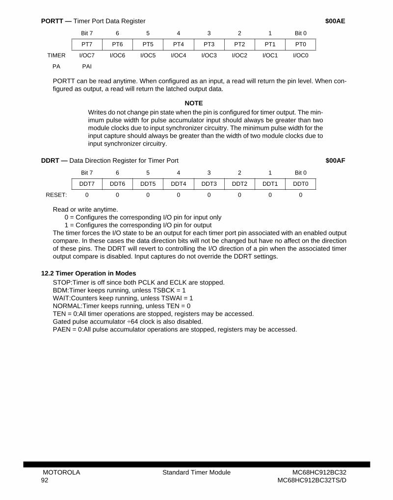
PORTT can be read anytime. When configured as an input, a read will return the pin level. When con-figured as output, a read will return the latched output data.
NOTEWrites do not change pin state when the pin is configured for timer output. The min-imum pulse width for pulse accumulator input should always be greater than twomodule clocks due to input synchronizer circuitry. The minimum pulse width for theinput capture should always be greater than the width of two module clocks due toinput synchronizer circuitry.
Read or write anytime.0 = Configures the corresponding I/O pin for input only 1 = Configures the corresponding I/O pin for output
The timer forces the I/O state to be an output for each timer port pin associated with an enabled outputcompare. In these cases the data direction bits will not be changed but have no affect on the directionof these pins. The DDRT will revert to controlling the I/O direction of a pin when the associated timeroutput compare is disabled. Input captures do not override the DDRT settings.
12.2 Timer Operation in ModesSTOP:Timer is off since both PCLK and ECLK are stopped. BDM:Timer keeps running, unless TSBCK = 1WAIT:Counters keep running, unless TSWAI = 1NORMAL:Timer keeps running, unless TEN = 0TEN = 0:All timer operations are stopped, registers may be accessed. Gated pulse accumulator ÷64 clock is also disabled.PAEN = 0:All pulse accumulator operations are stopped, registers may be accessed.
PORTT — Timer Port Data Register $00AE
Bit 7 6 5 4 3 2 1 Bit 0
PT7 PT6 PT5 PT4 PT3 PT2 PT1 PT0
TIMER I/OC7 I/OC6 I/OC5 I/OC4 I/OC3 I/OC2 I/OC1 I/OC0
PA PAI
DDRT — Data Direction Register for Timer Port $00AF
Bit 7 6 5 4 3 2 1 Bit 0
DDT7 DDT6 DDT5 DDT4 DDT3 DDT2 DDT1 DDT0
RESET: 0 0 0 0 0 0 0 0
MOTOROLA Standard Timer Module MC68HC912BC3292 MC68HC912BC32TS/D
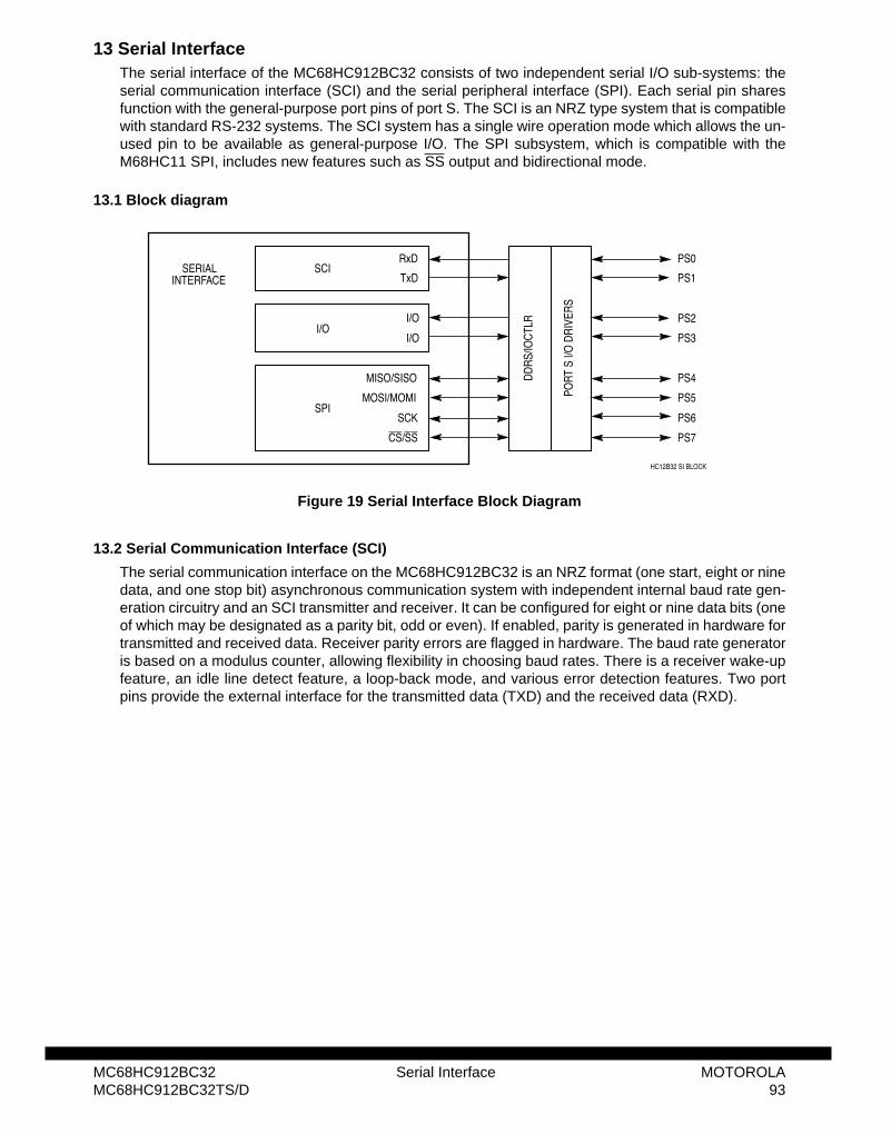
13 Serial InterfaceThe serial interface of the MC68HC912BC32 consists of two independent serial I/O sub-systems: theserial communication interface (SCI) and the serial peripheral interface (SPI). Each serial pin sharesfunction with the general-purpose port pins of port S. The SCI is an NRZ type system that is compatiblewith standard RS-232 systems. The SCI system has a single wire operation mode which allows the un-used pin to be available as general-purpose I/O. The SPI subsystem, which is compatible with theM68HC11 SPI, includes new features such as SS output and bidirectional mode.
13.1 Block diagram
Figure 19 Serial Interface Block Diagram
13.2 Serial Communication Interface (SCI)
The serial communication interface on the MC68HC912BC32 is an NRZ format (one start, eight or ninedata, and one stop bit) asynchronous communication system with independent internal baud rate gen-eration circuitry and an SCI transmitter and receiver. It can be configured for eight or nine data bits (oneof which may be designated as a parity bit, odd or even). If enabled, parity is generated in hardware fortransmitted and received data. Receiver parity errors are flagged in hardware. The baud rate generatoris based on a modulus counter, allowing flexibility in choosing baud rates. There is a receiver wake-upfeature, an idle line detect feature, a loop-back mode, and various error detection features. Two portpins provide the external interface for the transmitted data (TXD) and the received data (RXD).
SCI
I/O
SPI
DD
RS/
IOC
TLR
PORT
S I/
O D
RIV
ERS
SERIAL
HC12B32 SI BLOCK
INTERFACE
PS0
PS1
PS2
PS3
PS4
PS5
PS6
PS7
RxD
TxD
MISO/SISO
MOSI/MOMI
SCK
CS/SS
I/O
I/O
MC68HC912BC32 Serial Interface MOTOROLAMC68HC912BC32TS/D 93
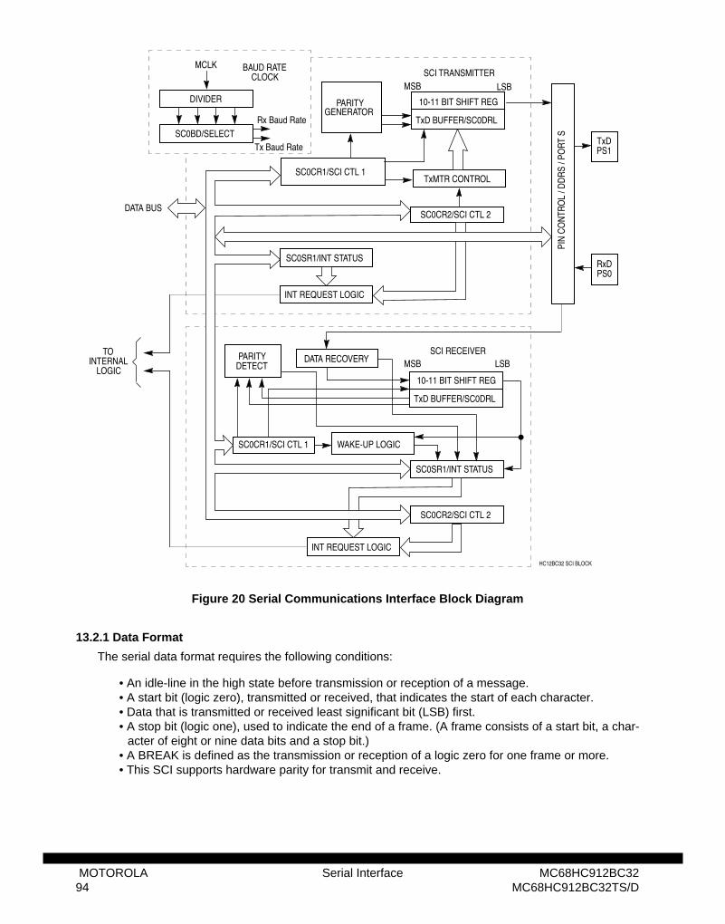
Figure 20 Serial Communications Interface Block Diagram
13.2.1 Data Format
The serial data format requires the following conditions:
• An idle-line in the high state before transmission or reception of a message.• A start bit (logic zero), transmitted or received, that indicates the start of each character.• Data that is transmitted or received least significant bit (LSB) first.• A stop bit (logic one), used to indicate the end of a frame. (A frame consists of a start bit, a char-
acter of eight or nine data bits and a stop bit.)• A BREAK is defined as the transmission or reception of a logic zero for one frame or more.• This SCI supports hardware parity for transmit and receive.
Rx Baud Rate
Tx Baud Rate
MCLK
DIVIDER 10-11 BIT SHIFT REG
MSB
TxD BUFFER/SC0DRL
TxMTR CONTROL
SC0CR2/SCI CTL 2
SC0CR1/SCI CTL 1
SC0SR1/INT STATUS
DATA RECOVERY
10-11 BIT SHIFT REG
TxD BUFFER/SC0DRL
SC0BD/SELECT
LSB
RxD
TxD
PIN
CO
NTR
OL
/ DD
RS
/ PO
RT S
WAKE-UP LOGICSC0CR1/SCI CTL 1
SC0SR1/INT STATUS
SC0CR2/SCI CTL 2
INT REQUEST LOGIC
MSB LSB
INT REQUEST LOGIC
SCI RECEIVER
SCI TRANSMITTER
DATA BUS
PARITYDETECT
PARITYGENERATOR
HC12BC32 SCI BLOCK
TO INTERNAL
LOGIC
BAUD RATECLOCK
PS0
PS1
MOTOROLA Serial Interface MC68HC912BC3294 MC68HC912BC32TS/D
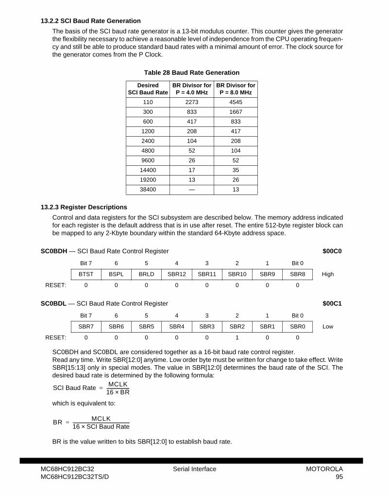
13.2.2 SCI Baud Rate Generation
The basis of the SCI baud rate generator is a 13-bit modulus counter. This counter gives the generatorthe flexibility necessary to achieve a reasonable level of independence from the CPU operating frequen-cy and still be able to produce standard baud rates with a minimal amount of error. The clock source forthe generator comes from the P Clock.
13.2.3 Register Descriptions
Control and data registers for the SCI subsystem are described below. The memory address indicatedfor each register is the default address that is in use after reset. The entire 512-byte register block canbe mapped to any 2-Kbyte boundary within the standard 64-Kbyte address space.
SC0BDH and SC0BDL are considered together as a 16-bit baud rate control register.Read any time. Write SBR[12:0] anytime. Low order byte must be written for change to take effect. WriteSBR[15:13] only in special modes. The value in SBR[12:0] determines the baud rate of the SCI. Thedesired baud rate is determined by the following formula:
which is equivalent to:
Table 28 Baud Rate Generation
DesiredSCI Baud Rate
BR Divisor forP = 4.0 MHz
BR Divisor forP = 8.0 MHz
110 2273 4545
300 833 1667
600 417 833
1200 208 417
2400 104 208
4800 52 104
9600 26 52
14400 17 35
19200 13 26
38400 — 13
SC0BDH — SCI Baud Rate Control Register $00C0
Bit 7 6 5 4 3 2 1 Bit 0
BTST BSPL BRLD SBR12 SBR11 SBR10 SBR9 SBR8 High
RESET: 0 0 0 0 0 0 0 0
SC0BDL — SCI Baud Rate Control Register $00C1
Bit 7 6 5 4 3 2 1 Bit 0
SBR7 SBR6 SBR5 SBR4 SBR3 SBR2 SBR1 SBR0 Low
RESET: 0 0 0 0 0 1 0 0
SCI Baud Rate MCLK16 BR×---------------------=
BR MCLK16 SCI Baud Rate×-----------------------------------------------------=
MC68HC912BC32 Serial Interface MOTOROLAMC68HC912BC32TS/D 95
BR is the value written to bits SBR[12:0] to establish baud rate.
NOTEThe baud rate generator is disabled until the TE or RE bit in SC0CR2 register is setfor the first time after reset, and/or the baud rate generator is disabled whenSBR[12:0] = 0.
BTST — Baud Register TestReserved for test function
BSPL — Baud Rate Counter SplitReserved for test function
BRLD — Baud Rate ReloadReserved for test function
Read or write anytime.
LOOPS — SCI LOOP Mode/Single Wire Mode Enable 0 = SCI transmit and receive sections operate normally.1 = SCI receive section is disconnected from the RXD pin and the RXD pin is available as general
purpose I/O. The receiver input is determined by the RSRC bit. The transmitter output is con-trolled by the associated DDRS bit. Both the transmitter and the receiver must be enabled touse the LOOP or the single wire mode.
If the DDRS bit associated with the TXD pin is set during the LOOPS = 1, the TXD pin outputs the SCIwaveform. If the DDRS bit associated with the TXD pin is clear during the LOOPS = 1, the TXD pin be-comes high (IDLE line state) for RSRC = 0 and high impedance for RSRC = 1. Refer to Table 29.
WOMS — Wired-Or Mode for Serial Pins This bit controls the two pins (TXD and RXD) associated with the SCI section.
0 = Pins operate in a normal mode with both high and low drive capability. To affect the RXD bit,that bit would have to be configured as an output (via DDRS) which is the single wire case whenusing the SCI. WOMS bit still affects general-purpose output on TXD and RXD pins when SCIis not using these pins.
1 = Each pin operates in an open drain fashion if that pin is declared as an output.
RSRC — Receiver SourceWhen LOOPS = 1, the RSRC bit determines the internal feedback path for the receiver.
0 = Receiver input is connected to the transmitter internally (not TXD pin)1 = Receiver input is connected to the TXD pin
SC0CR1 — SCI Control Register 1 $00C2
Bit 7 6 5 4 3 2 1 Bit 0
LOOPS WOMS RSRC M WAKE ILT PE PT
RESET: 0 0 0 0 0 0 0 0
MOTOROLA Serial Interface MC68HC912BC3296 MC68HC912BC32TS/D
M — Mode (select character format) 0 = One start, eight data, one stop bit1 = One start, eight data, ninth data, one stop bit
WAKE — Wakeup by Address Mark/Idle 0 = Wake up by IDLE line recognition 1 = Wake up by address mark (last data bit set)
ILT — Idle Line Type Determines which of two types of idle line detection will be used by the SCI receiver.
0 = Short idle line mode is enabled.1 = Long idle line mode is detected.
In the short mode, the SCI circuitry begins counting ones in the search for the idle line condition imme-diately after the start bit. This means that the stop bit and any bits that were ones before the stop bitcould be counted in that string of ones, resulting in earlier recognition of an idle line.In the long mode, the SCI circuitry does not begin counting ones in the search for the idle line conditionuntil a stop bit is received. Therefore, the last byte’s stop bit and preceding “1” bits do not affect howquickly an idle line condition can be detected.
PE — Parity Enable 0 = Parity is disabled.1 = Parity is enabled.
PT — Parity Type If parity is enabled, this bit determines even or odd parity for both the receiver and the transmitter.
0 = Even parity is selected. An even number of ones in the data character causes the parity bit tobe zero and an odd number of ones causes the parity bit to be one.
1 = Odd parity is selected. An odd number of ones in the data character causes the parity bit to bezero and an even number of ones causes the parity bit to be one.
Read or write anytime.
TIE — Transmit Interrupt Enable 0 = TDRE interrupts disabled
Table 29 Loop Mode Functions
LOOPS RSRC DDS1(3) WOMS Function of Port S Bit 1/3
0 x x x Normal Operations
1 0 0 0/1 LOOP mode without TXD output(TXD = High Impedance)
1 0 1 0 LOOP mode with TXD output (CMOS)
1 0 1 1 LOOP mode with TXD output (open-drain)
1 1 0 xSingle wire mode without TXD output
(the pin is used as receiver input only, TXD = High Impedance)
1 1 1 0Single wire mode with TXD output
(the output is also fed back to receiver input, CMOS)
1 1 1 1 Single wire mode for the receiving and transmitting(open-drain)
SC0CR2 — SCI Control Register 2 $00C3
Bit 7 6 5 4 3 2 1 Bit 0
TIE TCIE RIE ILIE TE RE RWU SBK
RESET: 0 0 0 0 0 0 0 0
MC68HC912BC32 Serial Interface MOTOROLAMC68HC912BC32TS/D 97
1 = SCI interrupt will be requested whenever the TDRE status flag is set.
TCIE — Transmit Complete Interrupt Enable 0 = TC interrupts disabled1 = SCI interrupt will be requested whenever the TC status flag is set.
RIE — Receiver Interrupt Enable 0 = RDRF and OR interrupts disabled1 = SCI interrupt will be requested whenever the RDRF status flag or the OR status flag is set.
ILIE — Idle Line Interrupt Enable 0 = IDLE interrupts disabled1 = SCI interrupt will be requested whenever the IDLE status flag is set.
TE — Transmitter Enable 0 = Transmitter disabled1 = SCI transmit logic is enabled and the TXD pin (Port S bit 1) is dedicated to the transmitter. The
TE bit can be used to queue an idle preamble.
RE — Receiver Enable 0 = Receiver disabled1 = Enables the SCI receive circuitry
RWU — Receiver Wake-Up Control0 = Normal SCI Receiver1 = Enables the wake-up function and inhibits further receiver interrupts. Normally hardware wakes
the receiver by automatically clearing this bit.
SBK — Send Break0 = Break generator off1 = Generate a break code (at least 10 or 11 contiguous zeros)
As long as SBK remains set the transmitter will send zeros. When SBK is changed to zero, the currentframe of all zeros is finished before the TxD line goes to the idle state. If SBK is toggled on and off, thetransmitter will send 10 (or 11) zeros and then revert to mark idle or sending data.
The bits in these registers are set by various conditions in the SCI hardware and are automaticallycleared by special acknowledge sequences. The receive related flag bits in SC0SR1 (RDRF, IDLE, OR,NF, FE, and PF) are all cleared by a read of the SC0SR1 register followed by a read of the transmit/receive data register L. However, only those bits which were set when SC0SR1 was read will be clearedby the subsequent read of the transmit/receive data register L. The transmit related bits in SC0SR1(TDRE and TC) are cleared by a read of the SC0SR1 register followed by a write to the transmit/receivedata register L.Read anytime (used in auto clearing mechanism). Write has no meaning or effect.
TDRE — Transmit Data Register Empty FlagNew data will not be transmitted unless SC0SR1 is read before writing to the transmit data register. Re-set sets this bit.
0 = SC0DR busy1 = Any byte in the transmit data register is transferred to the serial shift register so new data may
now be written to the transmit data register.
SC0SR1 — SCI Status Register 1 $00C4
Bit 7 6 5 4 3 2 1 Bit 0
TDRE TC RDRF IDLE OR NF FE PF
RESET: 1 1 0 0 0 0 0 0
MOTOROLA Serial Interface MC68HC912BC3298 MC68HC912BC32TS/D
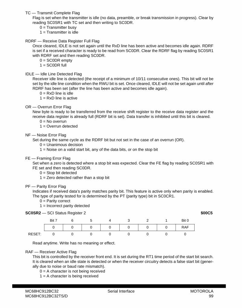
TC — Transmit Complete FlagFlag is set when the transmitter is idle (no data, preamble, or break transmission in progress). Clear byreading SC0SR1 with TC set and then writing to SC0DR.
0 = Transmitter busy1 = Transmitter is idle
RDRF — Receive Data Register Full FlagOnce cleared, IDLE is not set again until the RxD line has been active and becomes idle again. RDRFis set if a received character is ready to be read from SC0DR. Clear the RDRF flag by reading SC0SR1with RDRF set and then reading SC0DR.
0 = SC0DR empty1 = SC0DR full
IDLE — Idle Line Detected FlagReceiver idle line is detected (the receipt of a minimum of 10/11 consecutive ones). This bit will not beset by the idle line condition when the RWU bit is set. Once cleared, IDLE will not be set again until afterRDRF has been set (after the line has been active and becomes idle again).
0 = RxD line is idle1 = RxD line is active
OR — Overrun Error FlagNew byte is ready to be transferred from the receive shift register to the receive data register and thereceive data register is already full (RDRF bit is set). Data transfer is inhibited until this bit is cleared.
0 = No overrun1 = Overrun detected
NF — Noise Error FlagSet during the same cycle as the RDRF bit but not set in the case of an overrun (OR).
0 = Unanimous decision1 = Noise on a valid start bit, any of the data bits, or on the stop bit
FE — Framing Error FlagSet when a zero is detected where a stop bit was expected. Clear the FE flag by reading SC0SR1 withFE set and then reading SC0DR.
0 = Stop bit detected1 = Zero detected rather than a stop bit
PF — Parity Error FlagIndicates if received data’s parity matches parity bit. This feature is active only when parity is enabled.The type of parity tested for is determined by the PT (parity type) bit in SC0CR1.
0 = Parity correct1 = Incorrect parity detected
Read anytime. Write has no meaning or effect.
RAF — Receiver Active FlagThis bit is controlled by the receiver front end. It is set during the RT1 time period of the start bit search.It is cleared when an idle state is detected or when the receiver circuitry detects a false start bit (gener-ally due to noise or baud rate mismatch).
0 = A character is not being received
SC0SR2 — SCI Status Register 2 $00C5
Bit 7 6 5 4 3 2 1 Bit 0
0 0 0 0 0 0 0 RAF
RESET: 0 0 0 0 0 0 0 0
MC68HC912BC32 Serial Interface MOTOROLAMC68HC912BC32TS/D 99
1 = A character is being received
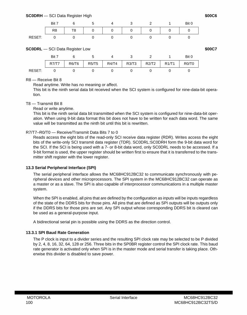
R8 — Receive Bit 8Read anytime. Write has no meaning or affect.This bit is the ninth serial data bit received when the SCI system is configured for nine-data-bit opera-tion.
T8 — Transmit Bit 8Read or write anytime.This bit is the ninth serial data bit transmitted when the SCI system is configured for nine-data-bit oper-ation. When using 9-bit data format this bit does not have to be written for each data word. The samevalue will be transmitted as the ninth bit until this bit is rewritten.
R7/T7–R0/T0 — Receive/Transmit Data Bits 7 to 0Reads access the eight bits of the read-only SCI receive data register (RDR). Writes access the eightbits of the write-only SCI transmit data register (TDR). SC0DRL:SC0DRH form the 9-bit data word forthe SCI. If the SCI is being used with a 7- or 8-bit data word, only SC0DRL needs to be accessed. If a9-bit format is used, the upper register should be written first to ensure that it is transferred to the trans-mitter shift register with the lower register.
13.3 Serial Peripheral Interface (SPI)
The serial peripheral interface allows the MC68HC912BC32 to communicate synchronously with pe-ripheral devices and other microprocessors. The SPI system in the MC68HC912BC32 can operate asa master or as a slave. The SPI is also capable of interprocessor communications in a multiple mastersystem.
When the SPI is enabled, all pins that are defined by the configuration as inputs will be inputs regardlessof the state of the DDRS bits for those pins. All pins that are defined as SPI outputs will be outputs onlyif the DDRS bits for those pins are set. Any SPI output whose corresponding DDRS bit is cleared canbe used as a general-purpose input.
A bidirectional serial pin is possible using the DDRS as the direction control.
13.3.1 SPI Baud Rate Generation
The P clock is input to a divider series and the resulting SPI clock rate may be selected to be P dividedby 2, 4, 8, 16, 32, 64, 128 or 256. Three bits in the SP0BR register control the SPI clock rate. This baudrate generator is activated only when SPI is in the master mode and serial transfer is taking place. Oth-erwise this divider is disabled to save power.
SC0DRH — SCI Data Register High $00C6
Bit 7 6 5 4 3 2 1 Bit 0
R8 T8 0 0 0 0 0 0
RESET: 0 0 0 0 0 0 0 0
SC0DRL — SCI Data Register Low $00C7
Bit 7 6 5 4 3 2 1 Bit 0
R7/T7 R6/T6 R5/T5 R4/T4 R3/T3 R2/T2 R1/T1 R0/T0
RESET: 0 0 0 0 0 0 0 0
MOTOROLA Serial Interface MC68HC912BC32100 MC68HC912BC32TS/D
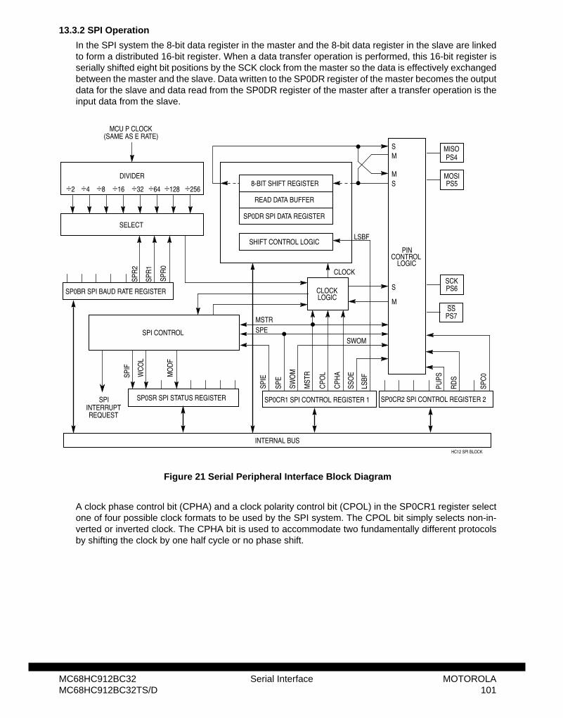
13.3.2 SPI Operation
In the SPI system the 8-bit data register in the master and the 8-bit data register in the slave are linkedto form a distributed 16-bit register. When a data transfer operation is performed, this 16-bit register isserially shifted eight bit positions by the SCK clock from the master so the data is effectively exchangedbetween the master and the slave. Data written to the SP0DR register of the master becomes the outputdata for the slave and data read from the SP0DR register of the master after a transfer operation is theinput data from the slave.
Figure 21 Serial Peripheral Interface Block Diagram
A clock phase control bit (CPHA) and a clock polarity control bit (CPOL) in the SP0CR1 register selectone of four possible clock formats to be used by the SPI system. The CPOL bit simply selects non-in-verted or inverted clock. The CPHA bit is used to accommodate two fundamentally different protocolsby shifting the clock by one half cycle or no phase shift.
PINCONTROL
LOGIC
8-BIT SHIFT REGISTER
READ DATA BUFFER
SHIFT CONTROL LOGIC
CLOCKLOGIC
SPI CONTROL
SP0SR SPI STATUS REGISTER
SP0DR SPI DATA REGISTER
SPIF
WC
OL
MO
DF
DIVIDER
SELECT
SP0BR SPI BAUD RATE REGISTER
÷2 ÷4 ÷8 ÷16 ÷32 ÷64 ÷128 ÷256
SPIINTERRUPT
INTERNAL BUS
MCU P CLOCK(SAME AS E RATE)
SM
M
S
M
S
SPR
2
SPR
1
SPR
0
REQUEST
SPIE
SPE
MST
R
CPO
L
CPH
A
LSBF
LSBF
PUPS
RD
S
SWO
M
SPC
0
SSO
E
SPE
CLOCK
MSTR
SWOM
MISOPS4
SCKPS6
SSPS7
MOSIPS5
HC12 SPI BLOCK
SP0CR1 SPI CONTROL REGISTER 1 SP0CR2 SPI CONTROL REGISTER 2
MC68HC912BC32 Serial Interface MOTOROLAMC68HC912BC32TS/D 101
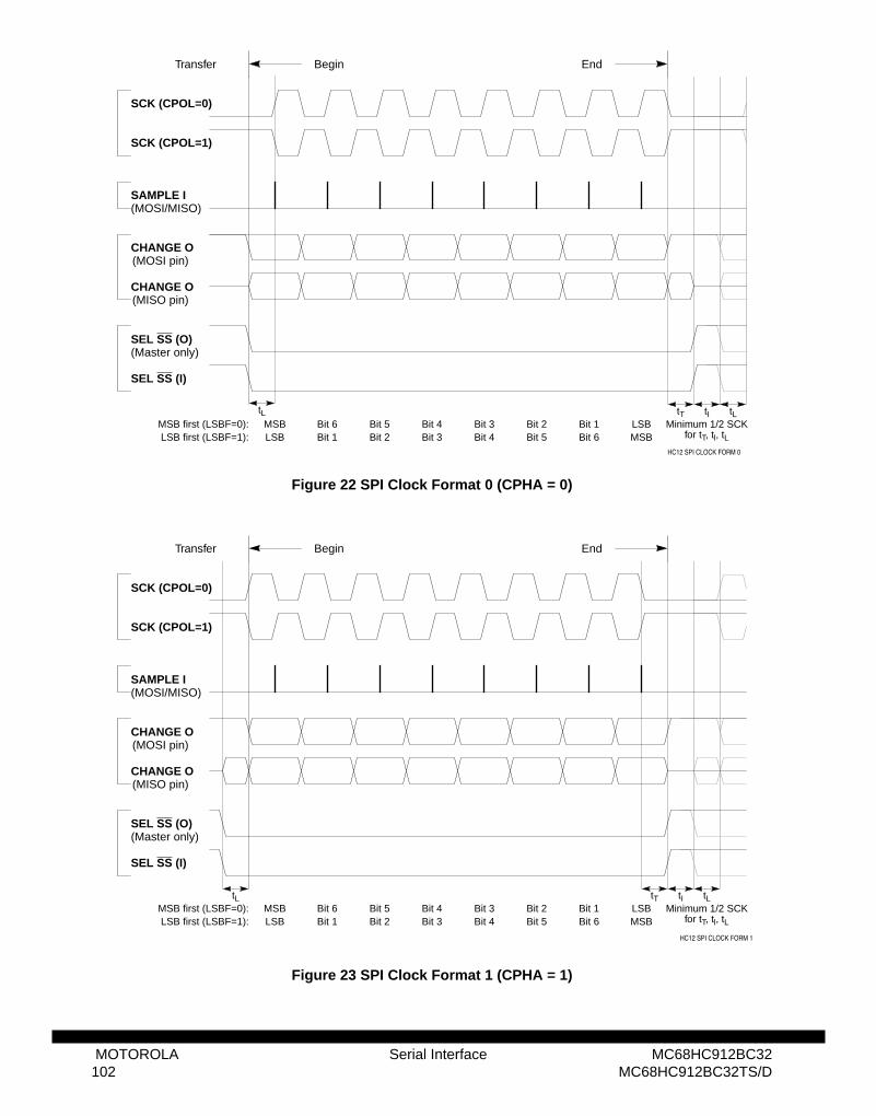
Figure 22 SPI Clock Format 0 (CPHA = 0)
Figure 23 SPI Clock Format 1 (CPHA = 1)
tL
Begin End
SCK (CPOL=0)
SAMPLE I
CHANGE O
SEL SS (O)
Transfer
SCK (CPOL=1)
MSB first (LSBF=0): LSB first (LSBF=1):
MSBLSB
LSBMSB
Bit 5Bit 2
Bit 6Bit 1
Bit 4Bit 3
Bit 3Bit 4
Bit 2Bit 5
Bit 1Bit 6
CHANGE O
SEL SS (I)
(MOSI pin)
(MISO pin)
(Master only)
(MOSI/MISO)
tT
for tT, tl, tLMinimum 1/2 SCK
tI tL
HC12 SPI CLOCK FORM 0
tL tT
for tT, tl, tLMinimum 1/2 SCK
tI tL
Begin End
SCK (CPOL=0)
SAMPLE I
CHANGE O
SEL SS (O)
Transfer
SCK (CPOL=1)
MSB first (LSBF=0): LSB first (LSBF=1):
MSBLSB
LSBMSB
Bit 5Bit 2
Bit 6Bit 1
Bit 4Bit 3
Bit 3Bit 4
Bit 2Bit 5
Bit 1Bit 6
CHANGE O
SEL SS (I)
(MOSI pin)
(MISO pin)
(Master only)
(MOSI/MISO)
HC12 SPI CLOCK FORM 1
MOTOROLA Serial Interface MC68HC912BC32102 MC68HC912BC32TS/D
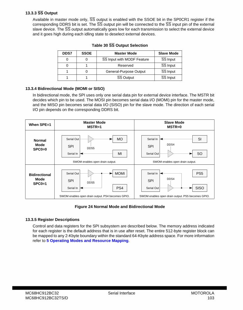
13.3.3 SS Output
Available in master mode only, SS output is enabled with the SSOE bit in the SP0CR1 register if thecorresponding DDRS bit is set. The SS output pin will be connected to the SS input pin of the externalslave device. The SS output automatically goes low for each transmission to select the external deviceand it goes high during each idling state to deselect external devices.
13.3.4 Bidirectional Mode (MOMI or SISO)
In bidirectional mode, the SPI uses only one serial data pin for external device interface. The MSTR bitdecides which pin to be used. The MOSI pin becomes serial data I/O (MOMI) pin for the master mode,and the MISO pin becomes serial data I/O (SISO) pin for the slave mode. The direction of each serialI/O pin depends on the corresponding DDRS bit.
Figure 24 Normal Mode and Bidirectional Mode
13.3.5 Register Descriptions
Control and data registers for the SPI subsystem are described below. The memory address indicatedfor each register is the default address that is in use after reset. The entire 512-byte register block canbe mapped to any 2-Kbyte boundary within the standard 64-Kbyte address space. For more informationrefer to 5 Operating Modes and Resource Mapping.
Table 30 SS Output Selection
DDS7 SSOE Master Mode Slave Mode
0 0 SS Input with MODF Feature SS Input
0 1 Reserved SS Input
1 0 General-Purpose Output SS Input
1 1 SS Output SS Input
When SPE=1Master Mode
MSTR=1Slave Mode
MSTR=0
NormalMode
SPC0=0
SWOM enables open drain output. SWOM enables open drain output.
Bidirectional Mode
SPC0=1
SWOM enables open drain output. PS4 becomes GPIO. SWOM enables open drain output. PS5 becomes GPIO.
SPI
MO
MI
DDS5
Serial Out
Serial In
SPI
SI
SO
Serial In
Serial Out
DDS4
SPI
MOMI
PS4
DDS5
Serial Out
Serial In
SPI
PS5
SISO
DDS4
Serial In
Serial Out
MC68HC912BC32 Serial Interface MOTOROLAMC68HC912BC32TS/D 103
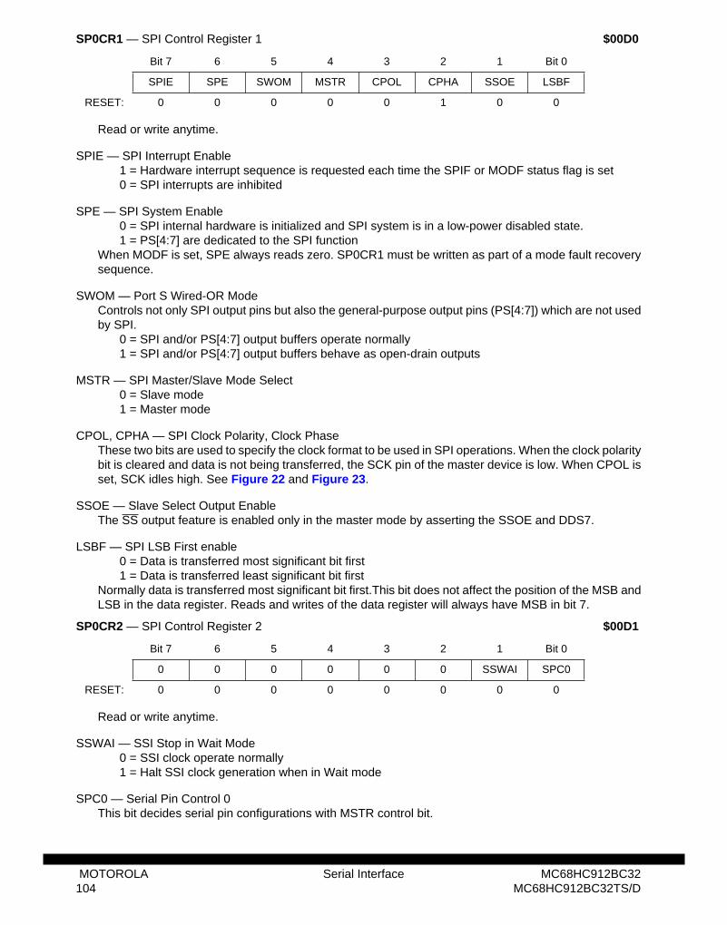
Read or write anytime.
SPIE — SPI Interrupt Enable1 = Hardware interrupt sequence is requested each time the SPIF or MODF status flag is set 0 = SPI interrupts are inhibited
SPE — SPI System Enable0 = SPI internal hardware is initialized and SPI system is in a low-power disabled state.1 = PS[4:7] are dedicated to the SPI function
When MODF is set, SPE always reads zero. SP0CR1 must be written as part of a mode fault recoverysequence.
SWOM — Port S Wired-OR ModeControls not only SPI output pins but also the general-purpose output pins (PS[4:7]) which are not usedby SPI.
0 = SPI and/or PS[4:7] output buffers operate normally1 = SPI and/or PS[4:7] output buffers behave as open-drain outputs
MSTR — SPI Master/Slave Mode Select0 = Slave mode1 = Master mode
CPOL, CPHA — SPI Clock Polarity, Clock PhaseThese two bits are used to specify the clock format to be used in SPI operations. When the clock polaritybit is cleared and data is not being transferred, the SCK pin of the master device is low. When CPOL isset, SCK idles high. See Figure 22 and Figure 23.
SSOE — Slave Select Output EnableThe SS output feature is enabled only in the master mode by asserting the SSOE and DDS7.
LSBF — SPI LSB First enable0 = Data is transferred most significant bit first1 = Data is transferred least significant bit first
Normally data is transferred most significant bit first.This bit does not affect the position of the MSB andLSB in the data register. Reads and writes of the data register will always have MSB in bit 7.
Read or write anytime.
SSWAI — SSI Stop in Wait Mode0 = SSI clock operate normally1 = Halt SSI clock generation when in Wait mode
SPC0 — Serial Pin Control 0This bit decides serial pin configurations with MSTR control bit.
SP0CR1 — SPI Control Register 1 $00D0
Bit 7 6 5 4 3 2 1 Bit 0
SPIE SPE SWOM MSTR CPOL CPHA SSOE LSBF
RESET: 0 0 0 0 0 1 0 0
SP0CR2 — SPI Control Register 2 $00D1
Bit 7 6 5 4 3 2 1 Bit 0
0 0 0 0 0 0 SSWAI SPC0
RESET: 0 0 0 0 0 0 0 0
MOTOROLA Serial Interface MC68HC912BC32104 MC68HC912BC32TS/D
Read anytime. Write anytime.At reset, E Clock divided by 2 is selected.
SPR[2:0] — SPI Clock (SCK) Rate Select BitsThese bits are used to specify the SPI clock rate.
Read anytime. Write has no meaning or effect.
SPIF — SPI Interrupt RequestSPIF is set after the eighth SCK cycle in a data transfer and it is cleared by reading the SP0SR register(with SPIF set) followed by an access (read or write) to the SPI data register.
NOTES:1. The serial pin control 0 bit enables bidirectional configurations.2. Slave output is enabled if DDS4 = 1, SS = 0 and MSTR = 0. (#1, #3)3. Master output is enabled if DDS5 = 1 and MSTR = 1. (#2, #4)4. SCK output is enabled if DDS6 = 1 and MSTR = 1. (#2, #4)5. SS output is enabled if DDS7 = 1, SSOE = 1 and MSTR = 1. (#2, #4)
Table 31
Pin Mode SPC01 MSTR MISO2 MOSI3 SCK4 SS5
#1Normal 0
0 Slave Out Slave In SCK In SS In
#2 1 Master In Master Out SCK Out SS I/O
#3Bidirectional 1
0 Slave I/O GPI/O SCK In SS In
#4 1 GPI/O Master I/O SCK Out SS I/O
SP0BR — SPI Baud Rate Register $00D2
Bit 7 6 5 4 3 2 1 Bit 0
0 0 0 0 0 SPR2 SPR1 SPR0
RESET: 0 0 0 0 0 0 0 0
Table 32 SPI Clock Rate Selection
SPR2 SPR1 SPR0E ClockDivisor
Frequency at E Clock = 4 MHz
Frequency at E Clock = 8 MHz
0 0 0 2 2.0 MHz 4.0 MHz
0 0 1 4 1.0 MHz 2.0 MHz
0 1 0 8 500 KHz 1.0 MHz
0 1 1 16 250 KHz 500 KHz
1 0 0 32 125 KHz 250 KHz
1 0 1 64 62.5 KHz 125 KHz
1 1 0 128 31.3 KHz 62.5 KHz
1 1 1 256 15.6 KHz 31.3 KHz
SP0SR — SPI Status Register $00D3
Bit 7 6 5 4 3 2 1 Bit 0
SPIF WCOL 0 MODF 0 0 0 0
RESET: 0 0 0 0 0 0 0 0
MC68HC912BC32 Serial Interface MOTOROLAMC68HC912BC32TS/D 105
WCOL — Write Collision Status FlagThe MCU write is disabled to avoid writing over the data being transferred. No interrupt is generatedbecause the error status flag can be read upon completion of the transfer that was in progress at thetime of the error. Automatically cleared by a read of the SP0SR (with WCOL set) followed by an access(read or write) to the SP0DR register.
0 = No write collision1 = Indicates that a serial transfer was in progress when the MCU tried to write new data into the
SP0DR data register.
MODF — SPI Mode Error Interrupt Status FlagThis bit is set automatically by SPI hardware if the MSTR control bit is set and the slave select input pinbecomes zero. This condition is not permitted in normal operation. In the case where DDRS bit 7 is set,the PS7 pin is a general-purpose output pin or SS output pin rather than being dedicated as the SS inputfor the SPI system. In this special case the mode fault function is inhibited and MODF remains cleared.This flag is automatically cleared by a read of the SP0SR (with MODF set) followed by a write to theSP0CR1 register.
Read anytime (normally only after SPIF flag set). Write anytime (see WCOL write collision flag).Reset does not affect this address.This 8-bit register is both the input and output register for SPI data. Reads of this register are doublebuffered but writes cause data to written directly into the serial shifter. In the SPI system the 8-bit dataregister in the master and the 8-bit data register in the slave are linked by the MOSI and MISO wires toform a distributed 16-bit register. When a data transfer operation is performed, this 16-bit register is se-rially shifted eight bit positions by the SCK clock from the master so the data is effectively exchangedbetween the master and the slave. Note that some slave devices are very simple and either accept datafrom the master without returning data to the master or pass data to the master without requiring datafrom the master.
13.4 Port S
In all modes, port S bits PS[7:0] can be used for either general-purpose I/O, or with the SCI and SPIsubsystems. During reset, port S pins are configured as high-impedance inputs (DDRS is cleared).
PORTS can be read anytime. When configured as an input, a read will return the pin level. When con-figured as output, a read will return the latched output data. Writes do not change pin state when pinconfigured for SPI or SCI output.After reset all bits are configured as general-purpose inputs.Port S shares function with the on-chip serial systems (SPI0 and SCI0).
SP0DR — SPI Data Register $00D5
Bit 7 6 5 4 3 2 1 Bit 0
Bit 7 6 5 4 3 2 1 Bit 0
RESET: 0 0 0 0 0 0 0 0
PORTS — Port S Data Register $00D6
Bit 7 6 5 4 3 2 1 Bit 0
PS7 PS6 PS5 PS4 PS3 PS2 PS1 PS0
PinFunction
SSCS SCK MOSI
MOMIMISOSISO I/O I/O TXD0 RXD0
MOTOROLA Serial Interface MC68HC912BC32106 MC68HC912BC32TS/D
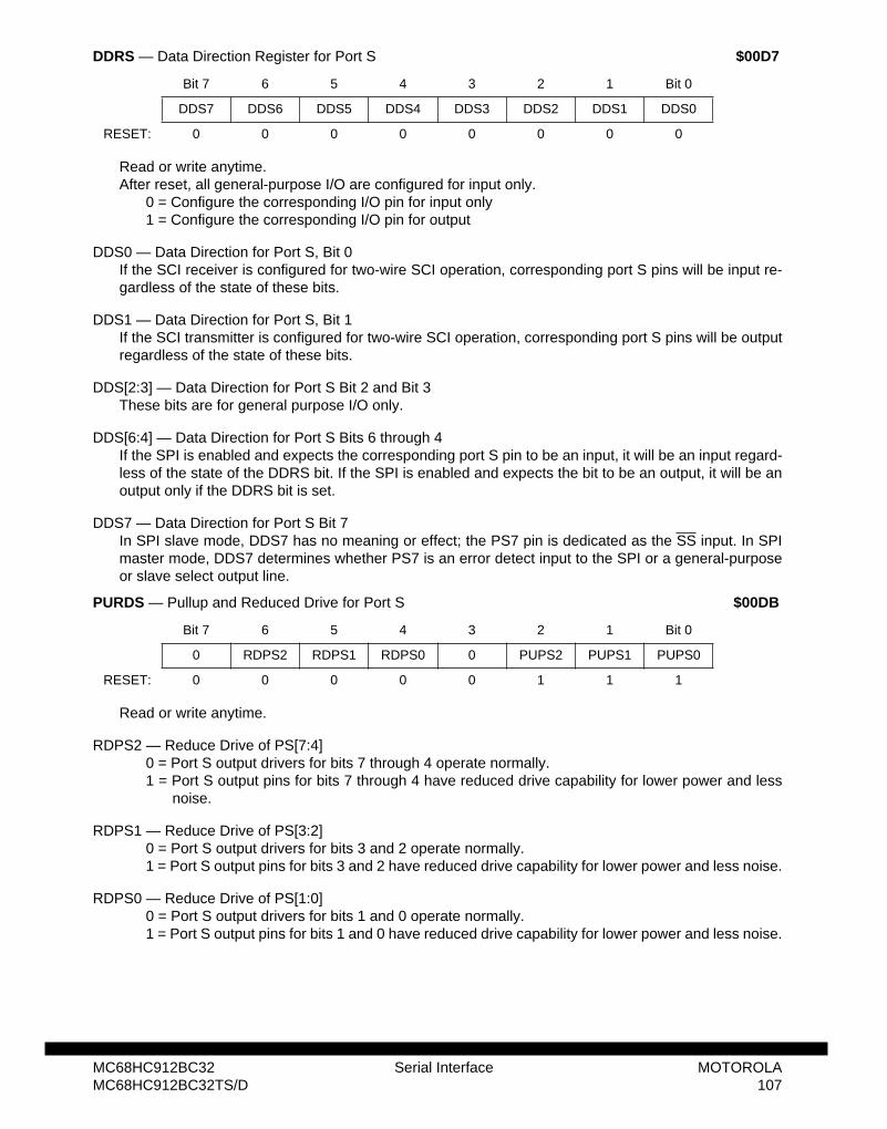
Read or write anytime.After reset, all general-purpose I/O are configured for input only.
0 = Configure the corresponding I/O pin for input only1 = Configure the corresponding I/O pin for output
DDS0 — Data Direction for Port S, Bit 0If the SCI receiver is configured for two-wire SCI operation, corresponding port S pins will be input re-gardless of the state of these bits.
DDS1 — Data Direction for Port S, Bit 1If the SCI transmitter is configured for two-wire SCI operation, corresponding port S pins will be outputregardless of the state of these bits.
DDS[2:3] — Data Direction for Port S Bit 2 and Bit 3These bits are for general purpose I/O only.
DDS[6:4] — Data Direction for Port S Bits 6 through 4If the SPI is enabled and expects the corresponding port S pin to be an input, it will be an input regard-less of the state of the DDRS bit. If the SPI is enabled and expects the bit to be an output, it will be anoutput only if the DDRS bit is set.
DDS7 — Data Direction for Port S Bit 7In SPI slave mode, DDS7 has no meaning or effect; the PS7 pin is dedicated as the SS input. In SPImaster mode, DDS7 determines whether PS7 is an error detect input to the SPI or a general-purposeor slave select output line.
Read or write anytime.
RDPS2 — Reduce Drive of PS[7:4]0 = Port S output drivers for bits 7 through 4 operate normally.1 = Port S output pins for bits 7 through 4 have reduced drive capability for lower power and less
noise.
RDPS1 — Reduce Drive of PS[3:2]0 = Port S output drivers for bits 3 and 2 operate normally.1 = Port S output pins for bits 3 and 2 have reduced drive capability for lower power and less noise.
RDPS0 — Reduce Drive of PS[1:0]0 = Port S output drivers for bits 1 and 0 operate normally.1 = Port S output pins for bits 1 and 0 have reduced drive capability for lower power and less noise.
DDRS — Data Direction Register for Port S $00D7
Bit 7 6 5 4 3 2 1 Bit 0
DDS7 DDS6 DDS5 DDS4 DDS3 DDS2 DDS1 DDS0
RESET: 0 0 0 0 0 0 0 0
PURDS — Pullup and Reduced Drive for Port S $00DB
Bit 7 6 5 4 3 2 1 Bit 0
0 RDPS2 RDPS1 RDPS0 0 PUPS2 PUPS1 PUPS0
RESET: 0 0 0 0 0 1 1 1
MC68HC912BC32 Serial Interface MOTOROLAMC68HC912BC32TS/D 107
PUPS2 — Pull-Up Port S Enable PS[7:4]0 = No internal pull-ups on port S bits 7 through 4.1 = Port S input pins for bits 7 through 4 have an active pull-up device. If a pin is programmed as
output, the pull-up device becomes inactive.
PUPS1 — Pull-Up Port S Enable PS[3:2]0 = No internal pull-ups on port S bits 3 and 2.1 = Port S input pins for bits 3 and 2 have an active pull-up device. If a pin is programmed as output,
the pull-up device becomes inactive.
PUPS0 — Pull-Up Port S Enable PS[1:0]0 = No internal pull-ups on port S bits 1 and 0.1 = Port S input pins for bits 1 and 0 have an active pull-up device. If a pin is programmed as output,
the pull-up device becomes inactive.
MOTOROLA Serial Interface MC68HC912BC32108 MC68HC912BC32TS/D
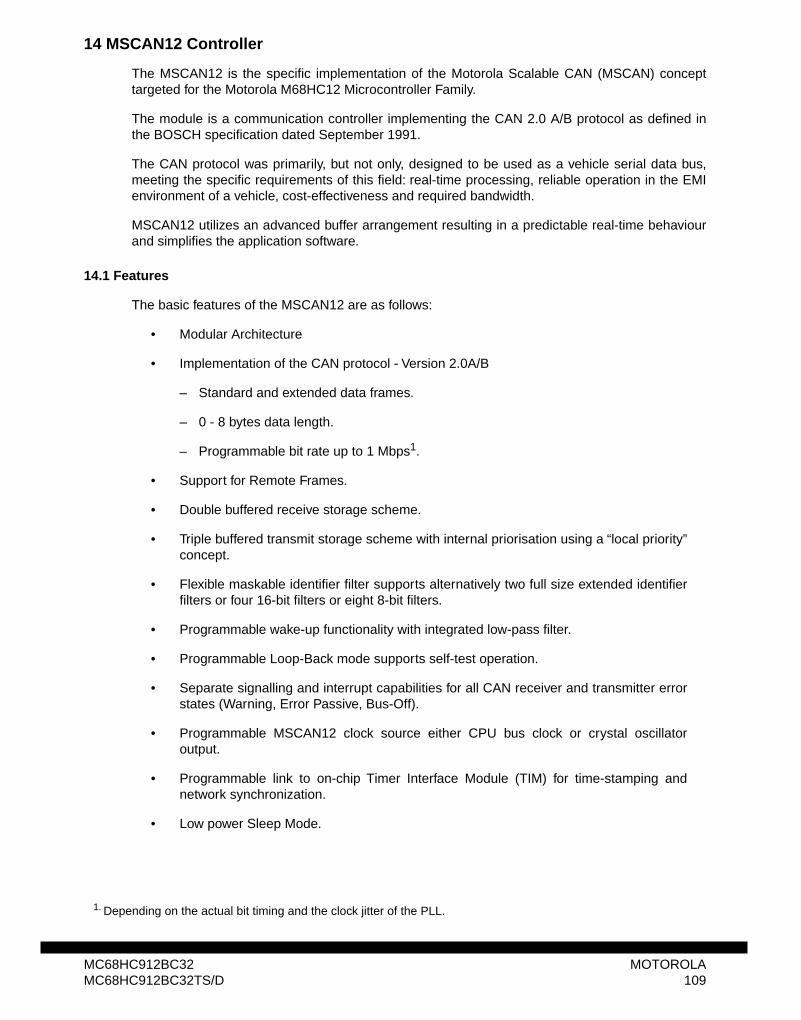
14 MSCAN12 Controller
The MSCAN12 is the specific implementation of the Motorola Scalable CAN (MSCAN) concepttargeted for the Motorola M68HC12 Microcontroller Family.
The module is a communication controller implementing the CAN 2.0 A/B protocol as defined inthe BOSCH specification dated September 1991.
The CAN protocol was primarily, but not only, designed to be used as a vehicle serial data bus,meeting the specific requirements of this field: real-time processing, reliable operation in the EMIenvironment of a vehicle, cost-effectiveness and required bandwidth.
MSCAN12 utilizes an advanced buffer arrangement resulting in a predictable real-time behaviourand simplifies the application software.
14.1 Features
The basic features of the MSCAN12 are as follows:
• Modular Architecture
• Implementation of the CAN protocol - Version 2.0A/B
– Standard and extended data frames.
– 0 - 8 bytes data length.
– Programmable bit rate up to 1 Mbps1.
• Support for Remote Frames.
• Double buffered receive storage scheme.
• Triple buffered transmit storage scheme with internal priorisation using a “local priority”concept.
• Flexible maskable identifier filter supports alternatively two full size extended identifierfilters or four 16-bit filters or eight 8-bit filters.
• Programmable wake-up functionality with integrated low-pass filter.
• Programmable Loop-Back mode supports self-test operation.
• Separate signalling and interrupt capabilities for all CAN receiver and transmitter errorstates (Warning, Error Passive, Bus-Off).
• Programmable MSCAN12 clock source either CPU bus clock or crystal oscillatoroutput.
• Programmable link to on-chip Timer Interface Module (TIM) for time-stamping andnetwork synchronization.
• Low power Sleep Mode.
MC68HC912BC32 MOTOROLAMC68HC912BC32TS/D 109
1. Depending on the actual bit timing and the clock jitter of the PLL.
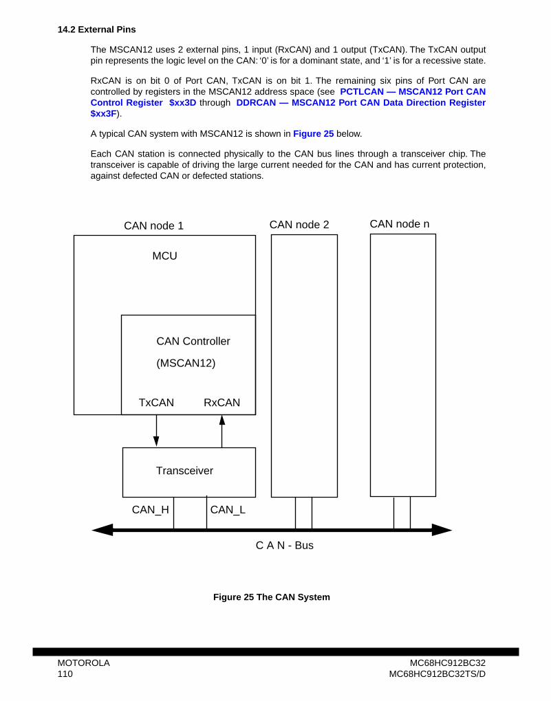
14.2 External Pins
The MSCAN12 uses 2 external pins, 1 input (RxCAN) and 1 output (TxCAN). The TxCAN outputpin represents the logic level on the CAN: ‘0’ is for a dominant state, and ‘1’ is for a recessive state.
RxCAN is on bit 0 of Port CAN, TxCAN is on bit 1. The remaining six pins of Port CAN arecontrolled by registers in the MSCAN12 address space (see PCTLCAN — MSCAN12 Port CANControl Register $xx3D through DDRCAN — MSCAN12 Port CAN Data Direction Register$xx3F).
A typical CAN system with MSCAN12 is shown in Figure 25 below.
Each CAN station is connected physically to the CAN bus lines through a transceiver chip. Thetransceiver is capable of driving the large current needed for the CAN and has current protection,against defected CAN or defected stations.
Figure 25 The CAN System
C A N - Bus
CAN Controller
(MSCAN12)
Transceiver
CAN node 1 CAN node 2 CAN node n
CAN_LCAN_H
TxCAN RxCAN
MCU
MOTOROLA MC68HC912BC32110 MC68HC912BC32TS/D
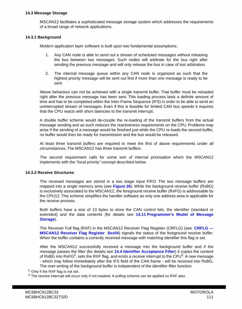
14.3 Message Storage
MSCAN12 facilitates a sophisticated message storage system which addresses the requirementsof a broad range of network applications.
14.3.1 Background
Modern application layer software is built upon two fundamental assumptions:
1. Any CAN node is able to send out a stream of scheduled messages without releasingthe bus between two messages. Such nodes will arbitrate for the bus right aftersending the previous message and will only release the bus in case of lost arbitration.
2. The internal message queue within any CAN node is organized as such that thehighest priority message will be sent out first if more than one message is ready to besent.
Above behaviour can not be achieved with a single transmit buffer. That buffer must be reloadedright after the previous message has been sent. This loading process lasts a definite amount oftime and has to be completed within the Inter-Frame Sequence (IFS) in order to be able to send anuninterrupted stream of messages. Even if this is feasible for limited CAN bus speeds it requiresthat the CPU reacts with short latencies to the transmit interrupt.
A double buffer scheme would de-couple the re-loading of the transmit buffers from the actualmessage sending and as such reduces the reactiveness requirements on the CPU. Problems mayarise if the sending of a message would be finished just while the CPU re-loads the second buffer,no buffer would then be ready for transmission and the bus would be released.
At least three transmit buffers are required to meet the first of above requirements under allcircumstances. The MSCAN12 has three transmit buffers.
The second requirement calls for some sort of internal priorisation which the MSCAN12implements with the “local priority” concept described below.
14.3.2 Receive Structures
The received messages are stored in a two stage input FIFO. The two message buffers aremapped into a single memory area (see Figure 26). While the background receive buffer (RxBG)is exclusively associated to the MSCAN12, the foreground receive buffer (RxFG) is addressable bythe CPU12. This scheme simplifies the handler software as only one address area is applicable forthe receive process.
Both buffers have a size of 13 bytes to store the CAN control bits, the identifier (standard orextended) and the data contents (for details see 14.11 Programmer’s Model of MessageStorage).
The Receiver Full flag (RXF) in the MSCAN12 Receiver Flag Register (CRFLG) (see CRFLG —MSCAN12 Receiver Flag Register $xx04) signals the status of the foreground receive buffer.When the buffer contains a correctly received message with matching identifier this flag is set.
After the MSCAN12 successfully received a message into the background buffer and if themessage passes the filter (for details see 14.4 Identifier Acceptance Filter) it copies the contentof RxBG into RxFG2, sets the RXF flag, and emits a receive interrupt to the CPU3. A new message- which may follow immediately after the IFS field of the CAN frame - will be received into RxBG.The over-writing of the background buffer is independent of the identifier filter function.
2. Only if the RXF flag is not set.
MC68HC912BC32 MOTOROLAMC68HC912BC32TS/D 111
3. The receive interrupt will occur only if not masked. A polling scheme can be applied on RXF also.
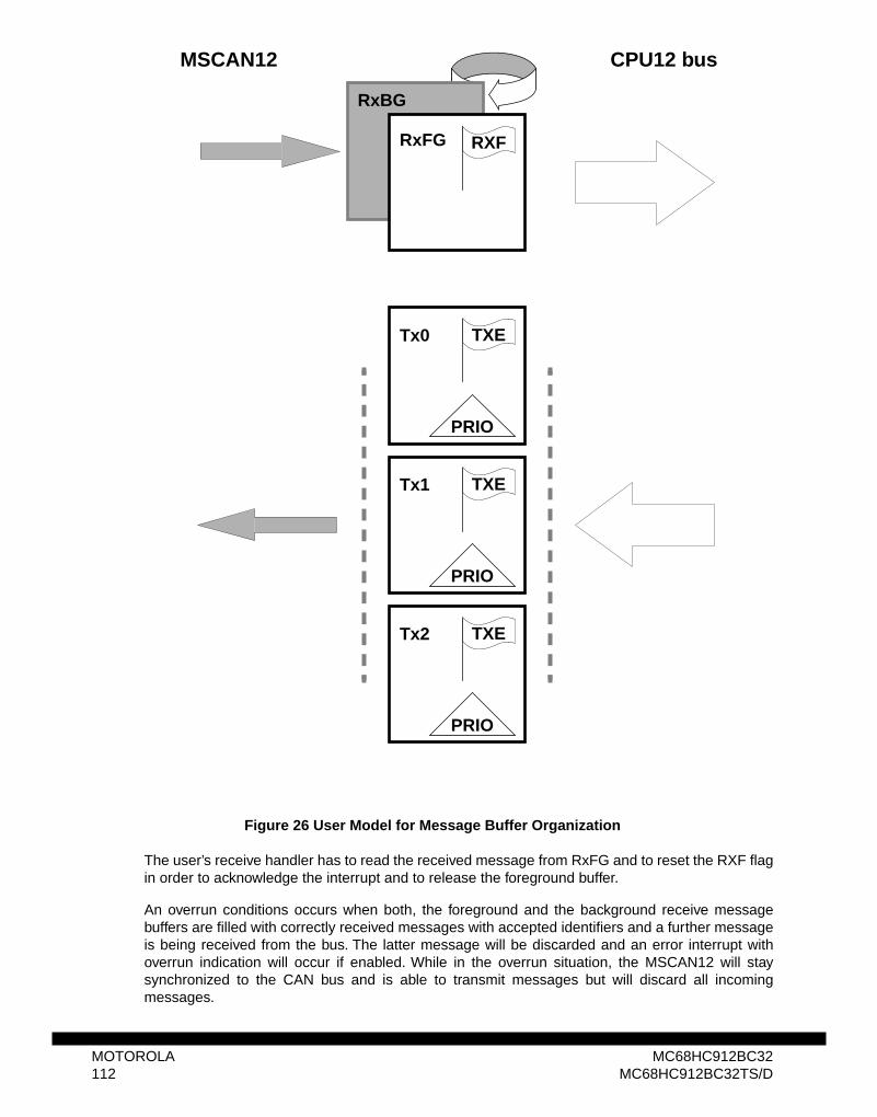
Figure 26 User Model for Message Buffer Organization
The user’s receive handler has to read the received message from RxFG and to reset the RXF flagin order to acknowledge the interrupt and to release the foreground buffer.
An overrun conditions occurs when both, the foreground and the background receive messagebuffers are filled with correctly received messages with accepted identifiers and a further messageis being received from the bus. The latter message will be discarded and an error interrupt withoverrun indication will occur if enabled. While in the overrun situation, the MSCAN12 will staysynchronized to the CAN bus and is able to transmit messages but will discard all incoming
RxFG
RxBG
Tx0
RXF
TXE
PRIO
Tx1 TXE
PRIO
Tx2 TXE
PRIO
MSCAN12 CPU12 bus
MOTOROLA MC68HC912BC32112 MC68HC912BC32TS/D
messages.
NOTEMSCAN12 will receive its own messages into the background receive buffer RxBGbut will NOT overwrite RxFG and will NOT emit a receive interrupt nor will it ac-knowledge (ACK) its own messages on the CAN bus. The exception to this rule isthat when in loop-back mode MSCAN12 will treat its own messages exactly like allother incoming messages.
14.3.3 Transmit Structures
The MSCAN12 has a triple transmit buffer scheme in order to allow multiple messages to be set upin advance and to achieve an optimized real-time performance. The three buffers are arranged asshown in Figure 26.
All three buffers have a 13 byte data structure similar to the outline of the receive buffers (see14.11 Programmer’s Model of Message Storage). An additional Transmit Buffer Priority Register(TBPR) contains an 8-bit so called “Local Priority” field (PRIO) (see TBPR — Transmit BufferPriority Registers $xxbD).
In order to transmit a message, the CPU12 has to identify an available transmit buffer which isindicated by a set Transmit Buffer Empty (TXE) Flag in the MSCAN12 Transmitter Flag Register(CTFLG) (see CTFLG — MSCAN12 Transmitter Flag Register $xx06).
The CPU12 then stores the identifier, the control bits and the data content into one of the transmitbuffers. Finally, the buffer has to be flagged as being ready for transmission by clearing the TXEflag.
The MSCAN12 will then schedule the message for transmission and will signal the successfultransmission of the buffer by setting the TXE flag. A transmit interrupt will be emitted4 when TXE isset and can be used to drive the application software to re-load the buffer.
In case more than one buffer is scheduled for transmission when the CAN bus becomes availablefor arbitration, the MSCAN12 uses the “local priority” setting of the three buffers for priorisation. Forthis purpose every transmit buffer has an 8-bit local priority field (PRIO). The application softwaresets this field when the message is set up. The local priority reflects the priority of this particularmessage relative to the set of messages being emitted from this node. The lowest binary value ofthe PRIO field is defined to be the highest priority.
The internal scheduling process takes places whenever the MSCAN12 arbitrates for the bus. Thisis also the case after the occurrence of a transmission error.
When a high priority message is scheduled by the application software it may become necessaryto abort a lower priority message being set up in one of the three transmit buffers. As messagesthat are already under transmission can not be aborted, the user has to request the abort bysetting the corresponding Abort Request Flag (ABTRQ) in the Transmission Control Register(CTCR). The MSCAN12 will then grant the request if possible by setting the corresponding AbortRequest Acknowledge (ABTAK) and the TXE flag in order to release the buffer and by emitting atransmit interrupt. The transmit interrupt handler software can tell from the setting of the ABTAKflag whether the message was actually aborted (ABTAK=1) or has been sent in the meantime(ABTAK=0).
MC68HC912BC32 MOTOROLAMC68HC912BC32TS/D 113
4. The transmit interrupt will occur only if not masked. A polling scheme can be applied on TXE also.
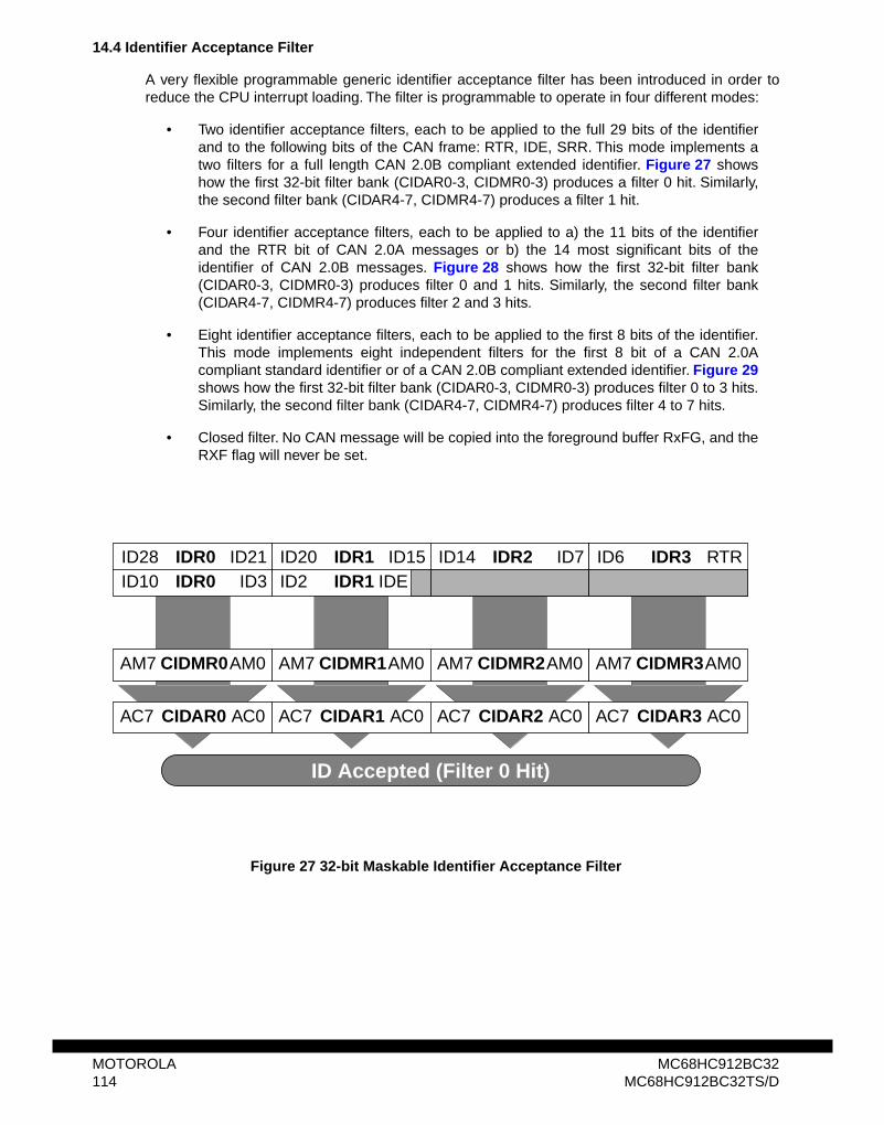
14.4 Identifier Acceptance Filter
A very flexible programmable generic identifier acceptance filter has been introduced in order toreduce the CPU interrupt loading. The filter is programmable to operate in four different modes:
• Two identifier acceptance filters, each to be applied to the full 29 bits of the identifierand to the following bits of the CAN frame: RTR, IDE, SRR. This mode implements atwo filters for a full length CAN 2.0B compliant extended identifier. Figure 27 showshow the first 32-bit filter bank (CIDAR0-3, CIDMR0-3) produces a filter 0 hit. Similarly,the second filter bank (CIDAR4-7, CIDMR4-7) produces a filter 1 hit.
• Four identifier acceptance filters, each to be applied to a) the 11 bits of the identifierand the RTR bit of CAN 2.0A messages or b) the 14 most significant bits of theidentifier of CAN 2.0B messages. Figure 28 shows how the first 32-bit filter bank(CIDAR0-3, CIDMR0-3) produces filter 0 and 1 hits. Similarly, the second filter bank(CIDAR4-7, CIDMR4-7) produces filter 2 and 3 hits.
• Eight identifier acceptance filters, each to be applied to the first 8 bits of the identifier.This mode implements eight independent filters for the first 8 bit of a CAN 2.0Acompliant standard identifier or of a CAN 2.0B compliant extended identifier. Figure 29shows how the first 32-bit filter bank (CIDAR0-3, CIDMR0-3) produces filter 0 to 3 hits.Similarly, the second filter bank (CIDAR4-7, CIDMR4-7) produces filter 4 to 7 hits.
• Closed filter. No CAN message will be copied into the foreground buffer RxFG, and theRXF flag will never be set.
Figure 27 32-bit Maskable Identifier Acceptance Filter
ID28 ID21IDR0ID10 ID3IDR0
ID20 ID15IDR1ID2 IDEIDR1
ID14 ID7IDR2ID10 ID3IDR2
ID6 RTRIDR3ID10 ID3IDR3
AC7 AC0CIDAR0
AM7 AM0CIDMR0
AC7 AC0CIDAR1
AM7 AM0CIDMR1
AC7 AC0CIDAR2
AM7 AM0CIDMR2
AC7 AC0CIDAR3
AM7 AM0CIDMR3
ID Accepted (Filter 0 Hit)
MOTOROLA MC68HC912BC32114 MC68HC912BC32TS/D
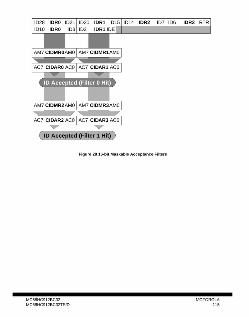
Figure 28 16-bit Maskable Acceptance Filters
ID28 ID21IDR0ID10 ID3IDR0
ID20 ID15IDR1ID2 IDEIDR1
ID14 ID7IDR2ID10 ID3IDR2
ID6 RTRIDR3ID10 ID3IDR3
AC7 AC0CIDAR0
AM7 AM0CIDMR0
AC7 AC0CIDAR1
AM7 AM0CIDMR1
ID Accepted (Filter 0 Hit)
AC7 AC0CIDAR2
AM7 AM0CIDMR2
AC7 AC0CIDAR3
AM7 AM0CIDMR3
ID Accepted (Filter 1 Hit)
MC68HC912BC32 MOTOROLAMC68HC912BC32TS/D 115
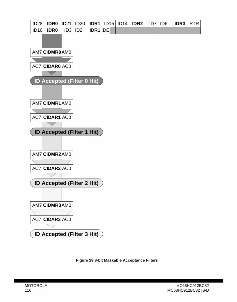
Figure 29 8-bit Maskable Acceptance Filters
AC7 AC0CIDAR3
AM7 AM0CIDMR3
ID Accepted (Filter 3 Hit)
AC7 AC0CIDAR2
AM7 AM0CIDMR2
ID Accepted (Filter 2 Hit)
AC7 AC0CIDAR1
AM7 AM0CIDMR1
ID Accepted (Filter 1 Hit)
ID28 ID21IDR0ID10 ID3IDR0
ID20 ID15IDR1ID2 IDEIDR1
ID14 ID7IDR2ID10 ID3IDR2
ID6 RTRIDR3ID10 ID3IDR3
AC7 AC0CIDAR0
AM7 AM0CIDMR0
ID Accepted (Filter 0 Hit)
MOTOROLA MC68HC912BC32116 MC68HC912BC32TS/D
The Identifier Acceptance Registers (CIDAR0-7) define the acceptable patterns of the standard orextended identifier (ID10 - ID0 or ID28 - ID0). Any of these bits can be marked ‘don’t care’ in theIdentifier Mask Registers (CIDMR0-7).
A filter hit is indicated to the application software by a set RXF (Receive Buffer Full Flag, see CRFLG — MSCAN12 Receiver Flag Register $xx04) and three bits in the Identifier AcceptanceControl Register (see CIDAC — MSCAN12 Identifier Acceptance Control Register $xx08).These Identifier Hit Flags (IDHIT2-0) clearly identify the filter section that caused the acceptance.They simplify the application software’s task to identify the cause of the receiver interrupt. In casethat more than one hit occurs (two or more filters match) the lower hit has priority.
A hit will also cause a receiver interrupt if enabled.
14.5 Interrupts
The MSCAN12 supports four interrupt vectors mapped onto eleven different interrupt sources, anyof which can be individually masked (for details see CRFLG — MSCAN12 Receiver FlagRegister $xx04 to CTCR — MSCAN12 Transmitter Control Register $xx07).
• Transmit Interrupt: At least one of the three transmit buffers is empty (not scheduled)and can be loaded to schedule a message for transmission. The TXE flags of theempty message buffers are set.
• Receive Interrupt: A message has been successfully received and loaded into theforeground receive buffer. This interrupt will be emitted immediately after receiving theEOF symbol. The RXF flag is set.
• Wake-Up Interrupt: An activity on the CAN bus occurred during MSCAN12 internalSleep Mode.
• Error Interrupt: An overrun, error or warning condition occurred. The Receiver FlagRegister (CRFLG) will indicate one of the following conditions:
– Overrun: An overrun condition as described in 14.3.2 Receive Structures hasoccurred.
– Receiver Warning: The Receive Error Counter has reached the CPU Warning limitof 96.
– Transmitter Warning: The Transmit Error Counter has reached the CPU Warninglimit of 96.
– Receiver Error Passive: The Receive Error Counter has exceeded the Error Passivelimit of 127 and MSCAN12 has gone to Error Passive state.
– Transmitter Error Passive: The Transmit Error Counter has exceeded the ErrorPassive limit of 127 and MSCAN12 has gone to Error Passive state.
– Bus Off: The Transmit Error Counter has exceeded 255 and MSCAN12 has gone toBus Off state.
MC68HC912BC32 MOTOROLAMC68HC912BC32TS/D 117
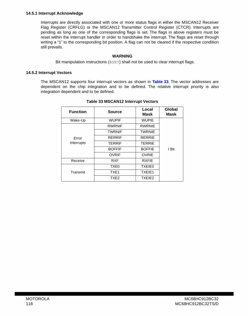
14.5.1 Interrupt Acknowledge
Interrupts are directly associated with one or more status flags in either the MSCAN12 ReceiverFlag Register (CRFLG) or the MSCAN12 Transmitter Control Register (CTCR). Interrupts arepending as long as one of the corresponding flags is set. The flags in above registers must bereset within the interrupt handler in order to handshake the interrupt. The flags are reset throughwriting a “1” to the corresponding bit position. A flag can not be cleared if the respective conditionstill prevails.
WARNINGBit manipulation instructions (BSET) shall not be used to clear interrupt flags.
14.5.2 Interrupt Vectors
The MSCAN12 supports four interrupt vectors as shown in Table 33. The vector addresses aredependent on the chip integration and to be defined. The relative interrupt priority is alsointegration dependent and to be defined.
Table 33 MSCAN12 Interrupt Vectors
Function SourceLocalMask
GlobalMask
Wake-Up WUPIF WUPIE
I Bit
ErrorInterrupts
RWRNIF RWRNIE
TWRNIF TWRNIE
RERRIF RERRIE
TERRIF TERRIE
BOFFIF BOFFIE
OVRIF OVRIE
Receive RXF RXFIE
Transmit
TXE0 TXEIE0
TXE1 TXEIE1
TXE2 TXEIE2
MOTOROLA MC68HC912BC32118 MC68HC912BC32TS/D
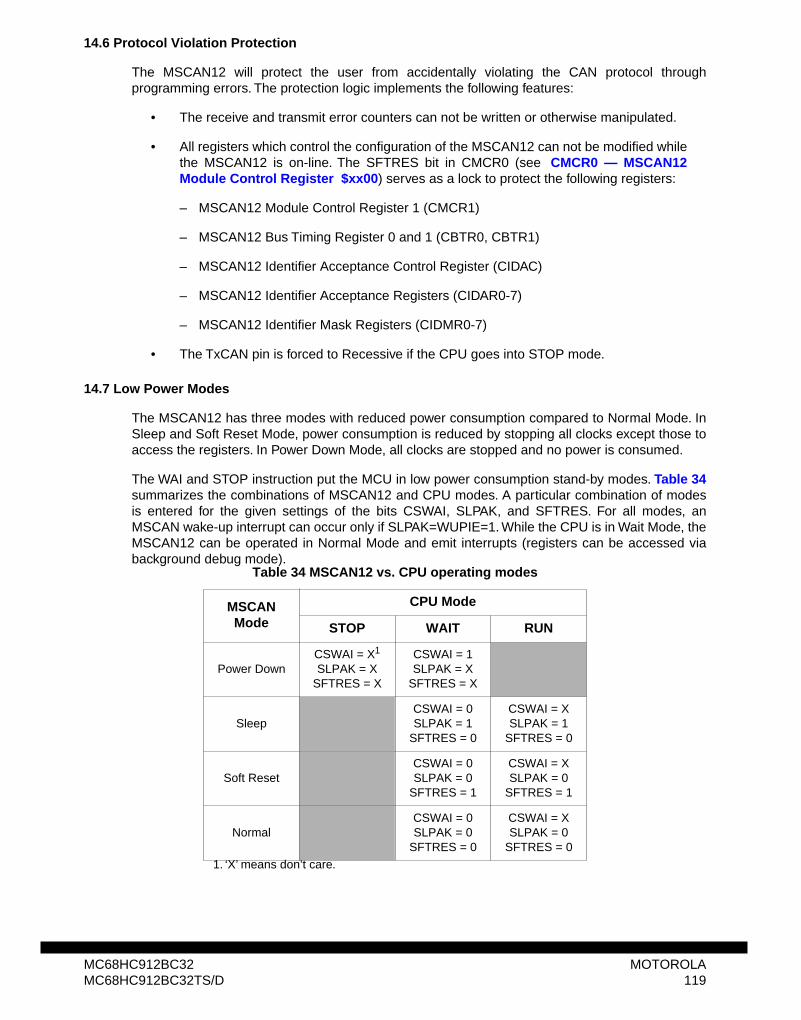
14.6 Protocol Violation Protection
The MSCAN12 will protect the user from accidentally violating the CAN protocol throughprogramming errors. The protection logic implements the following features:
• The receive and transmit error counters can not be written or otherwise manipulated.
• All registers which control the configuration of the MSCAN12 can not be modified whilethe MSCAN12 is on-line. The SFTRES bit in CMCR0 (see CMCR0 — MSCAN12Module Control Register $xx00) serves as a lock to protect the following registers:
– MSCAN12 Module Control Register 1 (CMCR1)
– MSCAN12 Bus Timing Register 0 and 1 (CBTR0, CBTR1)
– MSCAN12 Identifier Acceptance Control Register (CIDAC)
– MSCAN12 Identifier Acceptance Registers (CIDAR0-7)
– MSCAN12 Identifier Mask Registers (CIDMR0-7)
• The TxCAN pin is forced to Recessive if the CPU goes into STOP mode.
14.7 Low Power Modes
The MSCAN12 has three modes with reduced power consumption compared to Normal Mode. InSleep and Soft Reset Mode, power consumption is reduced by stopping all clocks except those toaccess the registers. In Power Down Mode, all clocks are stopped and no power is consumed.
The WAI and STOP instruction put the MCU in low power consumption stand-by modes. Table 34summarizes the combinations of MSCAN12 and CPU modes. A particular combination of modesis entered for the given settings of the bits CSWAI, SLPAK, and SFTRES. For all modes, anMSCAN wake-up interrupt can occur only if SLPAK=WUPIE=1. While the CPU is in Wait Mode, theMSCAN12 can be operated in Normal Mode and emit interrupts (registers can be accessed viabackground debug mode).
1. ‘X’ means don’t care.
Table 34 MSCAN12 vs. CPU operating modes
MSCAN Mode
CPU Mode
STOP WAIT RUN
Power DownCSWAI = X1
SLPAK = XSFTRES = X
CSWAI = 1SLPAK = X
SFTRES = X
SleepCSWAI = 0SLPAK = 1
SFTRES = 0
CSWAI = XSLPAK = 1
SFTRES = 0
Soft ResetCSWAI = 0SLPAK = 0
SFTRES = 1
CSWAI = XSLPAK = 0
SFTRES = 1
NormalCSWAI = 0SLPAK = 0
SFTRES = 0
CSWAI = XSLPAK = 0
SFTRES = 0
MC68HC912BC32 MOTOROLAMC68HC912BC32TS/D 119
14.7.1 MSCAN12 Sleep Mode
The CPU can request the MSCAN12 to enter this low-power mode by asserting the SLPRQ bit inthe Module Configuration Register (see Figure 30). The time when the MSCAN12 will then enterSleep Mode depends on its current activity:
• if it is transmitting, it will continue to transmit until there is no more message to betransmitted, and then go into Sleep Mode
• if it is receiving, it will wait for the end of this message and then go into Sleep Mode
• if it is neither transmitting nor receiving, it will immediately go into Sleep Mode
Figure 30 Sleep Request / Acknowledge Cycle
The application software must avoid to set up a transmission (by clearing one or more TXE flag(s))and immediately request Sleep Mode (by setting SLPRQ). It will then depend on the exactsequence of operations whether the MSCAN12 will start transmitting or go into Sleep Modedirectly.
During Sleep Mode, the SLPAK flag is set. The application software should use this flag as ahandshake indication for the request to go into Sleep Mode. When in Sleep Mode, the MSCAN12
MSCAN12 Running
SLPRQ = 0SLPAK = 0
Sleep Request
SLPRQ = 1SLPAK = 0
MSCAN12 Sleeping
SLPRQ = 1SLPAK = 1
MCU
MSCAN12
MCUor MSCAN12
MOTOROLA MC68HC912BC32120 MC68HC912BC32TS/D
stops its own clocks and the TxCAN pin will stay in recessive state.
The MSCAN12 will leave Sleep Mode (wake-up) when
• bus activity occurs or
• the MCU clears the SLPRQ bit.
NOTEThe MCU can not clear the SLPRQ bit before the MSCAN12 is in Sleep Mode(SLPAK = 1).
14.7.2 MSCAN12 Soft Reset Mode
In Soft Reset Mode, the MSCAN12 is stopped. Registers can still be accessed. This mode is usedto initialize the module configuration, bit timing, and the CAN message filter. See CMCR0 —MSCAN12 Module Control Register $xx00 for a complete description of the Soft Reset Mode.
14.7.3 MSCAN12 Power Down Mode
The MSCAN12 is in Power Down Mode when
• the CPU is in Stop Mode or
• the CPU is in Wait Mode and the CSWAI bit is set (see CMCR0 — MSCAN12 ModuleControl Register $xx00).
When entering the Power Down Mode, the MSCAN12 immediately stops all ongoing transmissionsand receptions, potentially causing CAN protocol violations. The user is responsible to take carethat the MSCAN12 is not active when Power Down Mode is entered. The recommended procedureis to bring the MSCAN12 into Sleep Mode before the STOP instruction - or the WAI instruction, ifCSWAI is set - is executed.
To protect the CAN bus system from fatal consequences of violations to above rule, the MSCAN12will drive the TxCAN pin into recessive state.
In Power Down Mode no registers can be accessed.
14.7.4 Programmable Wake-Up Function
The MSCAN12 can be programmed to apply a low-pass filter function to the RxCAN input linewhile in Sleep Mode (see control bit WUPM in the Module Control Register, CMCR0 —MSCAN12 Module Control Register $xx00). This feature can be used to protect the MSCAN12from wake-up due to short glitches on the CAN bus lines. Such glitches can result fromelectromagnetic inference within noisy environments.
MC68HC912BC32 MOTOROLAMC68HC912BC32TS/D 121
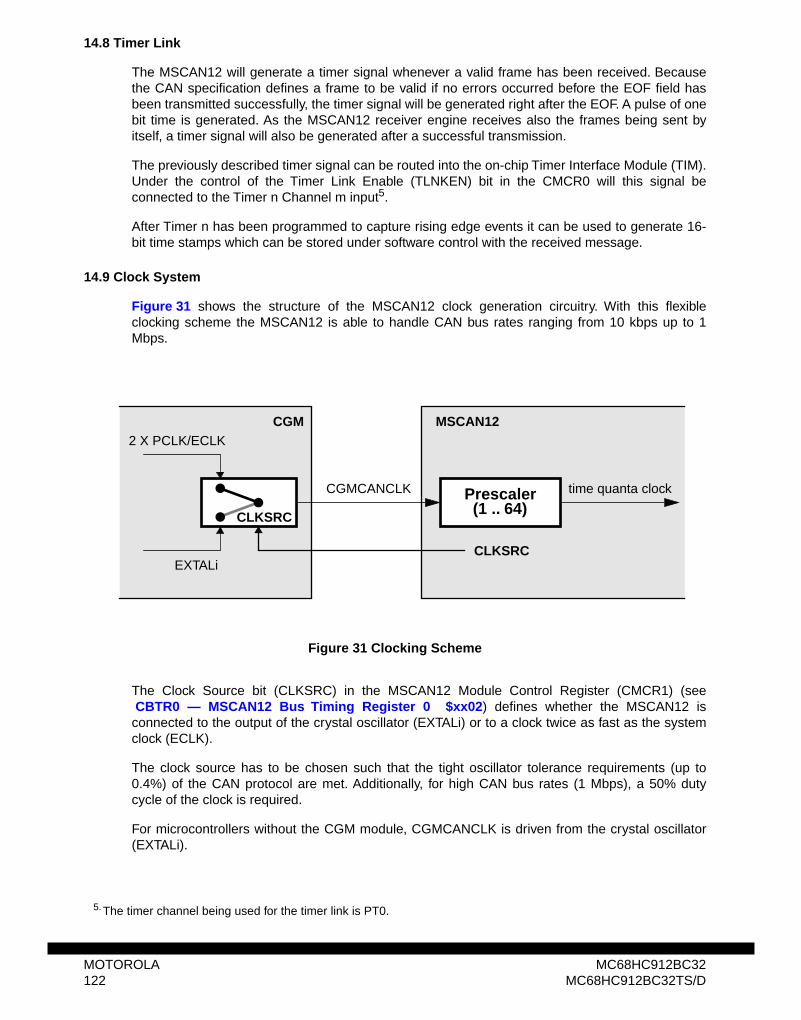
14.8 Timer Link
The MSCAN12 will generate a timer signal whenever a valid frame has been received. Becausethe CAN specification defines a frame to be valid if no errors occurred before the EOF field hasbeen transmitted successfully, the timer signal will be generated right after the EOF. A pulse of onebit time is generated. As the MSCAN12 receiver engine receives also the frames being sent byitself, a timer signal will also be generated after a successful transmission.
The previously described timer signal can be routed into the on-chip Timer Interface Module (TIM).Under the control of the Timer Link Enable (TLNKEN) bit in the CMCR0 will this signal beconnected to the Timer n Channel m input5.
After Timer n has been programmed to capture rising edge events it can be used to generate 16-bit time stamps which can be stored under software control with the received message.
14.9 Clock System
Figure 31 shows the structure of the MSCAN12 clock generation circuitry. With this flexibleclocking scheme the MSCAN12 is able to handle CAN bus rates ranging from 10 kbps up to 1Mbps.
Figure 31 Clocking Scheme
The Clock Source bit (CLKSRC) in the MSCAN12 Module Control Register (CMCR1) (see CBTR0 — MSCAN12 Bus Timing Register 0 $xx02) defines whether the MSCAN12 isconnected to the output of the crystal oscillator (EXTALi) or to a clock twice as fast as the systemclock (ECLK).
The clock source has to be chosen such that the tight oscillator tolerance requirements (up to0.4%) of the CAN protocol are met. Additionally, for high CAN bus rates (1 Mbps), a 50% dutycycle of the clock is required.
For microcontrollers without the CGM module, CGMCANCLK is driven from the crystal oscillator(EXTALi).
Prescaler(1 .. 64)CLKSRC
CGMCANCLK time quanta clock
2 X PCLK/ECLK
EXTALi
CGM MSCAN12
CLKSRC
MOTOROLA MC68HC912BC32122 MC68HC912BC32TS/D
5. The timer channel being used for the timer link is PT0.
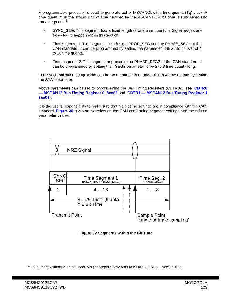
A programmable prescaler is used to generate out of MSCANCLK the time quanta (Tq) clock. Atime quantum is the atomic unit of time handled by the MSCAN12. A bit time is subdivided intothree segments6:
• SYNC_SEG: This segment has a fixed length of one time quantum. Signal edges areexpected to happen within this section.
• Time segment 1: This segment includes the PROP_SEG and the PHASE_SEG1 of theCAN standard. It can be programmed by setting the parameter TSEG1 to consist of 4to 16 time quanta.
• Time segment 2: This segment represents the PHASE_SEG2 of the CAN standard. Itcan be programmed by setting the TSEG2 parameter to be 2 to 8 time quanta long.
The Synchronization Jump Width can be programmed in a range of 1 to 4 time quanta by settingthe SJW parameter.
Above parameters can be set by programming the Bus Timing Registers (CBTR0-1, see CBTR0— MSCAN12 Bus Timing Register 0 $xx02 and CBTR1 — MSCAN12 Bus Timing Register 1$xx03).
It is the user’s responsibility to make sure that his bit time settings are in compliance with the CANstandard. Figure 35 gives an overview on the CAN conforming segment settings and the relatedparameter values.
Figure 32 Segments within the Bit Time
SYNC_SEG Time Segment 1 Time Seg. 2
1 4 ... 16 2 ... 8
8... 25 Time Quanta= 1 Bit Time
NRZ Signal
Sample Point (single or triple sampling)
(PROP_SEG + PHASE_SEG1) (PHASE_SEG2)
Transmit Point
MC68HC912BC32 MOTOROLAMC68HC912BC32TS/D 123
6. For further explanation of the under-lying concepts please refer to ISO/DIS 11519-1, Section 10.3.
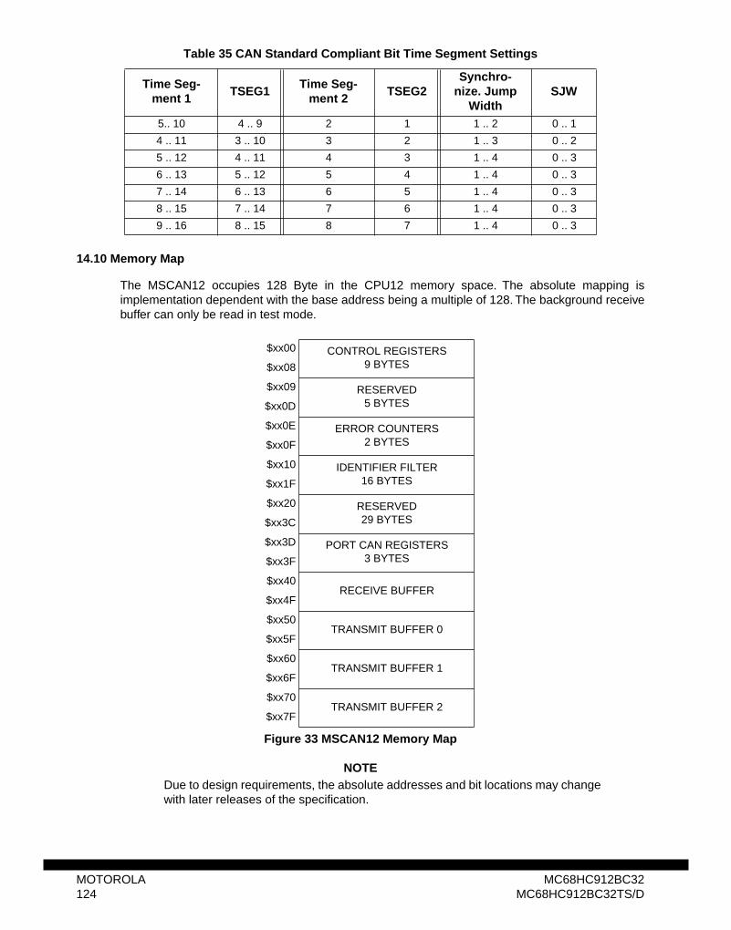
14.10 Memory Map
The MSCAN12 occupies 128 Byte in the CPU12 memory space. The absolute mapping isimplementation dependent with the base address being a multiple of 128. The background receivebuffer can only be read in test mode.
NOTEDue to design requirements, the absolute addresses and bit locations may changewith later releases of the specification.
Table 35 CAN Standard Compliant Bit Time Segment Settings
Time Seg-ment 1
TSEG1Time Seg-
ment 2TSEG2
Synchro-nize. Jump
WidthSJW
5.. 10 4 .. 9 2 1 1 .. 2 0 .. 1
4 .. 11 3 .. 10 3 2 1 .. 3 0 .. 2
5 .. 12 4 .. 11 4 3 1 .. 4 0 .. 3
6 .. 13 5 .. 12 5 4 1 .. 4 0 .. 3
7 .. 14 6 .. 13 6 5 1 .. 4 0 .. 3
8 .. 15 7 .. 14 7 6 1 .. 4 0 .. 3
9 .. 16 8 .. 15 8 7 1 .. 4 0 .. 3
$xx00 CONTROL REGISTERS9 BYTES$xx08
$xx09 RESERVED5 BYTES$xx0D
$xx0E ERROR COUNTERS2 BYTES$xx0F
$xx10 IDENTIFIER FILTER16 BYTES$xx1F
$xx20 RESERVED29 BYTES$xx3C
$xx3D PORT CAN REGISTERS3 BYTES$xx3F
$xx40RECEIVE BUFFER
$xx4F
$xx50TRANSMIT BUFFER 0
$xx5F
$xx60TRANSMIT BUFFER 1
$xx6F
$xx70TRANSMIT BUFFER 2
$xx7F
Figure 33 MSCAN12 Memory Map
MOTOROLA MC68HC912BC32124 MC68HC912BC32TS/D
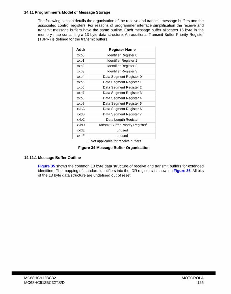
14.11 Programmer’s Model of Message Storage
The following section details the organisation of the receive and transmit message buffers and theassociated control registers. For reasons of programmer interface simplification the receive andtransmit message buffers have the same outline. Each message buffer allocates 16 byte in thememory map containing a 13 byte data structure. An additional Transmit Buffer Priority Register(TBPR) is defined for the transmit buffers.
14.11.1 Message Buffer Outline
Figure 35 shows the common 13 byte data structure of receive and transmit buffers for extendedidentifiers. The mapping of standard identifiers into the IDR registers is shown in Figure 36. All bitsof the 13 byte data structure are undefined out of reset.
Addr Register Namexxb0 Identifier Register 0
xxb1 Identifier Register 1
xxb2 Identifier Register 2
xxb3 Identifier Register 3
xxb4 Data Segment Register 0
xxb5 Data Segment Register 1
xxb6 Data Segment Register 2
xxb7 Data Segment Register 3
xxb8 Data Segment Register 4
xxb9 Data Segment Register 5
xxbA Data Segment Register 6
xxbB Data Segment Register 7
xxbC Data Length Register
xxbD Transmit Buffer Priority Register1
xxbE unused
xxbF unused
1. Not applicable for receive buffers
Figure 34 Message Buffer Organisation
MC68HC912BC32 MOTOROLAMC68HC912BC32TS/D 125
14.11.2 Identifier Registers (IDRn)
The identifiers consist of either 11 bits (ID10 – ID0) for the standard, or 29 bits (ID28 - ID0) for theextended format. ID10/28 is the most significant bit and is transmitted first on the bus during thearbitration procedure. The priority of an identifier is defined to be highest for the smallest binarynumber.
SRR - Substitute Remote RequestThis fixed recessive bit is used only in extended format. It must be set to 1 by the user fortransmission buffers and will be stored as received on the CAN bus for receive buffers.
IDE — ID ExtendedThis flag indicates whether the extended or standard identifier format is applied in this buffer. Incase of a receive buffer the flag is set as being received and indicates to the CPU how toprocess the buffer identifier registers. In case of a transmit buffer the flag indicates to theMSCAN12 what type of identifier to send.
1 = Extended format (29 bit)0 = Standard format (11 bit)
Figure 35 Receive / Transmit Message Buffer Extended Identifier
Address Bit 7 6 5 4 3 2 1 Bit 0 Name
$xxb0 ID28 ID27 ID26 ID25 ID24 ID23 ID22 ID21 IDR0
$xxb1 ID20 ID19 ID18 SRR (1) IDE (1) ID17 ID16 ID15 IDR1
$xxb2 ID14 ID13 ID12 ID11 ID10 ID9 ID8 ID7 IDR2
$xxb3 ID6 ID5 ID4 ID3 ID2 ID1 ID0 RTR IDR3
$xxb4 DB7 DB6 DB5 DB4 DB3 DB2 DB1 DB0 DSR0
$xxb5 DB7 DB6 DB5 DB4 DB3 DB2 DB1 DB0 DSR1
$xxb6 DB7 DB6 DB5 DB4 DB3 DB2 DB1 DB0 DSR2
$xxb7 DB7 DB6 DB5 DB4 DB3 DB2 DB1 DB0 DSR3
$xxb8 DB7 DB6 DB5 DB4 DB3 DB2 DB1 DB0 DSR4
$xxb9 DB7 DB6 DB5 DB4 DB3 DB2 DB1 DB0 DSR5
$xxbA DB7 DB6 DB5 DB4 DB3 DB2 DB1 DB0 DSR6
$xxbB DB7 DB6 DB5 DB4 DB3 DB2 DB1 DB0 DSR7
$xxbC DLC3 DLC2 DLC1 DLC0 DLR
Figure 36 Standard Identifier Mapping
Address Bit 7 6 5 4 3 2 1 Bit 0 Name
$xxb0 ID10 ID9 ID8 ID7 ID6 ID5 ID4 ID3 IDR0
$xxb1 ID2 ID1 ID0 RTR IDE(0) IDR1
$xxb2 IDR2
$xxb3 IDR3
MOTOROLA MC68HC912BC32126 MC68HC912BC32TS/D
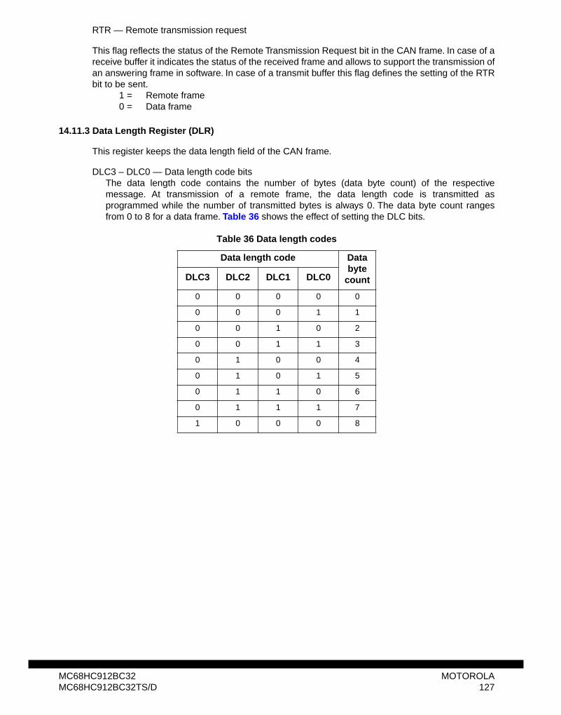
RTR — Remote transmission request
This flag reflects the status of the Remote Transmission Request bit in the CAN frame. In case of areceive buffer it indicates the status of the received frame and allows to support the transmission ofan answering frame in software. In case of a transmit buffer this flag defines the setting of the RTRbit to be sent.
1 = Remote frame0 = Data frame
14.11.3 Data Length Register (DLR)
This register keeps the data length field of the CAN frame.
DLC3 – DLC0 — Data length code bitsThe data length code contains the number of bytes (data byte count) of the respectivemessage. At transmission of a remote frame, the data length code is transmitted asprogrammed while the number of transmitted bytes is always 0. The data byte count rangesfrom 0 to 8 for a data frame. Table 36 shows the effect of setting the DLC bits.
Table 36 Data length codes
Data length code Data byte
countDLC3 DLC2 DLC1 DLC0
0 0 0 0 0
0 0 0 1 1
0 0 1 0 2
0 0 1 1 3
0 1 0 0 4
0 1 0 1 5
0 1 1 0 6
0 1 1 1 7
1 0 0 0 8
MC68HC912BC32 MOTOROLAMC68HC912BC32TS/D 127
14.11.4 Data Segment Registers (DSRn)
The eight data segment registers contain the data to be transmitted or being received. The numberof bytes to be transmitted or being received is determined by the data length code in thecorresponding DLR.
TBPR — Transmit Buffer Priority Registers $xxbD
PRIO7 - PRIO0— Local PriorityThis field defines the local priority of the associated message buffer. The local priority is usedfor the internal priorisation process of the MSCAN12 and is defined to be highest for thesmallest binary number. The MSCAN12 implements the following internal priorisationmechanism:
• All transmission buffers with a cleared TXE flag participate in the priorisation rightbefore the SOF (Start of Frame) is sent.
• The transmission buffer with the lowest local priority field wins the priorisation.
• In case of more than one buffer having the same lowest priority the message bufferwith the lower index number wins.
WARNINGTo ensure data integrity, no registers of the transmit buffers shall be written whilethe associated TXE flag is cleared. Similarly, to ensure data integrity, no registersof the receive buffer shall be read while the RXF flag is cleared.
Bit 7 6 5 4 3 2 1 Bit 0
PRIO7 PRIO6 PRIO5 PRIO4 PRIO3 PRIO2 PRIO1 PRIO0
RESET: U U U U U U U U
MOTOROLA MC68HC912BC32128 MC68HC912BC32TS/D
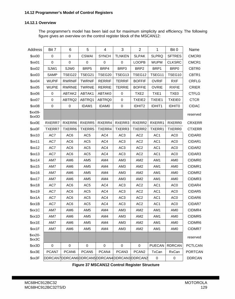
14.12 Programmer’s Model of Control Registers
14.12.1 Overview
The programmer’s model has been laid out for maximum simplicity and efficiency. The followingfigure gives an overview on the control register block of the MSCAN12:
Address Bit 7 6 5 4 3 2 1 Bit 0 Name
$xx00 0 0 CSWAI SYNCH TLNKEN SLPAK SLPRQ SFTRES CMCR0
$xx01 0 0 0 0 0 LOOPB WUPM CLKSRC CMCR1
$xx02 SJW1 SJW0 BRP5 BRP4 BRP3 BRP2 BRP1 BRP0 CBTR0
$xx03 SAMP TSEG22 TSEG21 TSEG20 TSEG13 TSEG12 TSEG11 TSEG10 CBTR1
$xx04 WUPIF RWRNIF TWRNIF RERRIF TERRIF BOFFIF OVRIF RXF CRFLG
$xx05 WUPIE RWRNIE TWRNIE RERRIE TERRIE BOFFIE OVRIE RXFIE CRIER
$xx06 0 ABTAK2 ABTAK1 ABTAK0 0 TXE2 TXE1 TXE0 CTFLG
$xx07 0 ABTRQ2 ABTRQ1 ABTRQ0 0 TXEIE2 TXEIE1 TXEIE0 CTCR
$xx08 0 0 IDAM1 IDAM0 0 IDHIT2 IDHIT1 IDHIT0 CIDAC
$xx09-$xx0D
reserved
$xx0E RXERR7 RXERR6 RXERR5 RXERR4 RXERR3 RXERR2 RXERR1 RXERR0 CRXERR
$xx0F TXERR7 TXERR6 TXERR5 TXERR4 TXERR3 TXERR2 TXERR1 TXERR0 CTXERR
$xx10 AC7 AC6 AC5 AC4 AC3 AC2 AC1 AC0 CIDAR0
$xx11 AC7 AC6 AC5 AC4 AC3 AC2 AC1 AC0 CIDAR1
$xx12 AC7 AC6 AC5 AC4 AC3 AC2 AC1 AC0 CIDAR2
$xx13 AC7 AC6 AC5 AC4 AC3 AC2 AC1 AC0 CIDAR3
$xx14 AM7 AM6 AM5 AM4 AM3 AM2 AM1 AM0 CIDMR0
$xx15 AM7 AM6 AM5 AM4 AM3 AM2 AM1 AM0 CIDMR1
$xx16 AM7 AM6 AM5 AM4 AM3 AM2 AM1 AM0 CIDMR2
$xx17 AM7 AM6 AM5 AM4 AM3 AM2 AM1 AM0 CIDMR3
$xx18 AC7 AC6 AC5 AC4 AC3 AC2 AC1 AC0 CIDAR4
$xx19 AC7 AC6 AC5 AC4 AC3 AC2 AC1 AC0 CIDAR5
$xx1A AC7 AC6 AC5 AC4 AC3 AC2 AC1 AC0 CIDAR6
$xx1B AC7 AC6 AC5 AC4 AC3 AC2 AC1 AC0 CIDAR7
$xx1C AM7 AM6 AM5 AM4 AM3 AM2 AM1 AM0 CIDMR4
$xx1D AM7 AM6 AM5 AM4 AM3 AM2 AM1 AM0 CIDMR5
$xx1E AM7 AM6 AM5 AM4 AM3 AM2 AM1 AM0 CIDMR6
$xx1F AM7 AM6 AM5 AM4 AM3 AM2 AM1 AM0 CIDMR7
$xx20-$xx3C
reserved
$xx3D 0 0 0 0 0 0 PUECAN RDRCAN PCTLCAN
$xx3E PCAN7 PCAN6 PCAN5 PCAN4 PCAN3 PCAN2 TxCan RxCan PORTCAN
$xx3F DDRCAN7DDRCAN6DDRCAN5DDRCAN4 DDRCAN3 DDRCAN2 0 0 DDRCAN
MC68HC912BC32 MOTOROLAMC68HC912BC32TS/D 129
Figure 37 MSCAN12 Control Register Structure
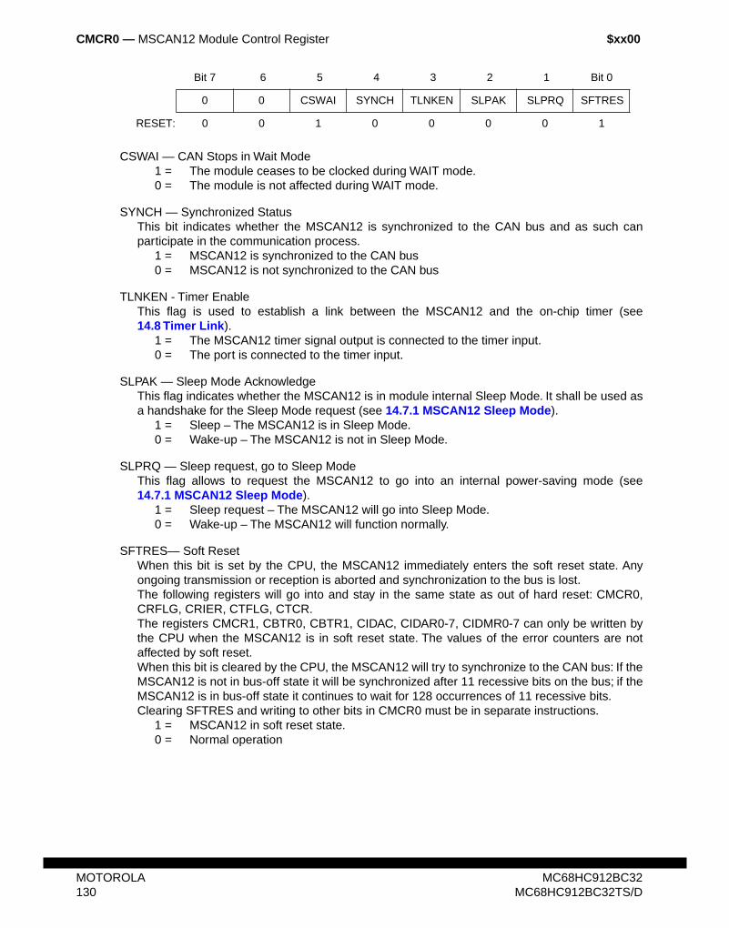
CMCR0 — MSCAN12 Module Control Register $xx00
CSWAI — CAN Stops in Wait Mode1 = The module ceases to be clocked during WAIT mode.0 = The module is not affected during WAIT mode.
SYNCH — Synchronized StatusThis bit indicates whether the MSCAN12 is synchronized to the CAN bus and as such canparticipate in the communication process.
1 = MSCAN12 is synchronized to the CAN bus0 = MSCAN12 is not synchronized to the CAN bus
TLNKEN - Timer EnableThis flag is used to establish a link between the MSCAN12 and the on-chip timer (see14.8 Timer Link).
1 = The MSCAN12 timer signal output is connected to the timer input.0 = The port is connected to the timer input.
SLPAK — Sleep Mode AcknowledgeThis flag indicates whether the MSCAN12 is in module internal Sleep Mode. It shall be used asa handshake for the Sleep Mode request (see 14.7.1 MSCAN12 Sleep Mode).
1 = Sleep – The MSCAN12 is in Sleep Mode.0 = Wake-up – The MSCAN12 is not in Sleep Mode.
SLPRQ — Sleep request, go to Sleep ModeThis flag allows to request the MSCAN12 to go into an internal power-saving mode (see14.7.1 MSCAN12 Sleep Mode).
1 = Sleep request – The MSCAN12 will go into Sleep Mode.0 = Wake-up – The MSCAN12 will function normally.
SFTRES— Soft Reset When this bit is set by the CPU, the MSCAN12 immediately enters the soft reset state. Anyongoing transmission or reception is aborted and synchronization to the bus is lost. The following registers will go into and stay in the same state as out of hard reset: CMCR0,CRFLG, CRIER, CTFLG, CTCR. The registers CMCR1, CBTR0, CBTR1, CIDAC, CIDAR0-7, CIDMR0-7 can only be written bythe CPU when the MSCAN12 is in soft reset state. The values of the error counters are notaffected by soft reset.When this bit is cleared by the CPU, the MSCAN12 will try to synchronize to the CAN bus: If theMSCAN12 is not in bus-off state it will be synchronized after 11 recessive bits on the bus; if theMSCAN12 is in bus-off state it continues to wait for 128 occurrences of 11 recessive bits.Clearing SFTRES and writing to other bits in CMCR0 must be in separate instructions.
1 = MSCAN12 in soft reset state.0 = Normal operation
Bit 7 6 5 4 3 2 1 Bit 0
0 0 CSWAI SYNCH TLNKEN SLPAK SLPRQ SFTRES
RESET: 0 0 1 0 0 0 0 1
MOTOROLA MC68HC912BC32130 MC68HC912BC32TS/D
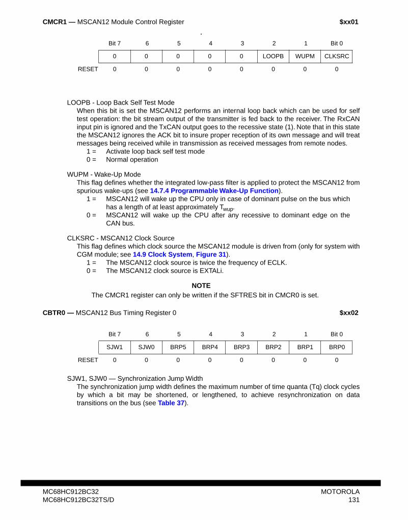
CMCR1 — MSCAN12 Module Control Register $xx01
.
LOOPB - Loop Back Self Test ModeWhen this bit is set the MSCAN12 performs an internal loop back which can be used for selftest operation: the bit stream output of the transmitter is fed back to the receiver. The RxCANinput pin is ignored and the TxCAN output goes to the recessive state (1). Note that in this statethe MSCAN12 ignores the ACK bit to insure proper reception of its own message and will treatmessages being received while in transmission as received messages from remote nodes.
1 = Activate loop back self test mode0 = Normal operation
WUPM - Wake-Up ModeThis flag defines whether the integrated low-pass filter is applied to protect the MSCAN12 fromspurious wake-ups (see 14.7.4 Programmable Wake-Up Function).
1 = MSCAN12 will wake up the CPU only in case of dominant pulse on the bus whichhas a length of at least approximately Twup.
0 = MSCAN12 will wake up the CPU after any recessive to dominant edge on theCAN bus.
CLKSRC - MSCAN12 Clock SourceThis flag defines which clock source the MSCAN12 module is driven from (only for system withCGM module; see 14.9 Clock System, Figure 31).
1 = The MSCAN12 clock source is twice the frequency of ECLK.0 = The MSCAN12 clock source is EXTALi.
NOTEThe CMCR1 register can only be written if the SFTRES bit in CMCR0 is set.
CBTR0 — MSCAN12 Bus Timing Register 0 $xx02
SJW1, SJW0 — Synchronization Jump WidthThe synchronization jump width defines the maximum number of time quanta (Tq) clock cyclesby which a bit may be shortened, or lengthened, to achieve resynchronization on datatransitions on the bus (see Table 37).
Bit 7 6 5 4 3 2 1 Bit 0
0 0 0 0 0 LOOPB WUPM CLKSRC
RESET 0 0 0 0 0 0 0 0
Bit 7 6 5 4 3 2 1 Bit 0
SJW1 SJW0 BRP5 BRP4 BRP3 BRP2 BRP1 BRP0
RESET 0 0 0 0 0 0 0 0
MC68HC912BC32 MOTOROLAMC68HC912BC32TS/D 131
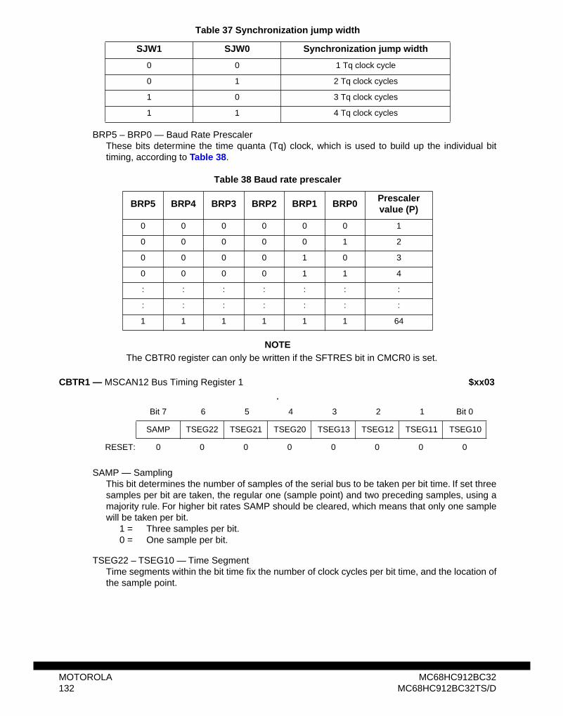
BRP5 – BRP0 — Baud Rate PrescalerThese bits determine the time quanta (Tq) clock, which is used to build up the individual bittiming, according to Table 38.
NOTEThe CBTR0 register can only be written if the SFTRES bit in CMCR0 is set.
CBTR1 — MSCAN12 Bus Timing Register 1 $xx03
.
SAMP — SamplingThis bit determines the number of samples of the serial bus to be taken per bit time. If set threesamples per bit are taken, the regular one (sample point) and two preceding samples, using amajority rule. For higher bit rates SAMP should be cleared, which means that only one samplewill be taken per bit.
1 = Three samples per bit.0 = One sample per bit.
TSEG22 – TSEG10 — Time SegmentTime segments within the bit time fix the number of clock cycles per bit time, and the location ofthe sample point.
Table 37 Synchronization jump width
SJW1 SJW0 Synchronization jump width
0 0 1 Tq clock cycle
0 1 2 Tq clock cycles
1 0 3 Tq clock cycles
1 1 4 Tq clock cycles
Table 38 Baud rate prescaler
BRP5 BRP4 BRP3 BRP2 BRP1 BRP0Prescaler value (P)
0 0 0 0 0 0 1
0 0 0 0 0 1 2
0 0 0 0 1 0 3
0 0 0 0 1 1 4
: : : : : : :
: : : : : : :
1 1 1 1 1 1 64
Bit 7 6 5 4 3 2 1 Bit 0
SAMP TSEG22 TSEG21 TSEG20 TSEG13 TSEG12 TSEG11 TSEG10
RESET: 0 0 0 0 0 0 0 0
MOTOROLA MC68HC912BC32132 MC68HC912BC32TS/D
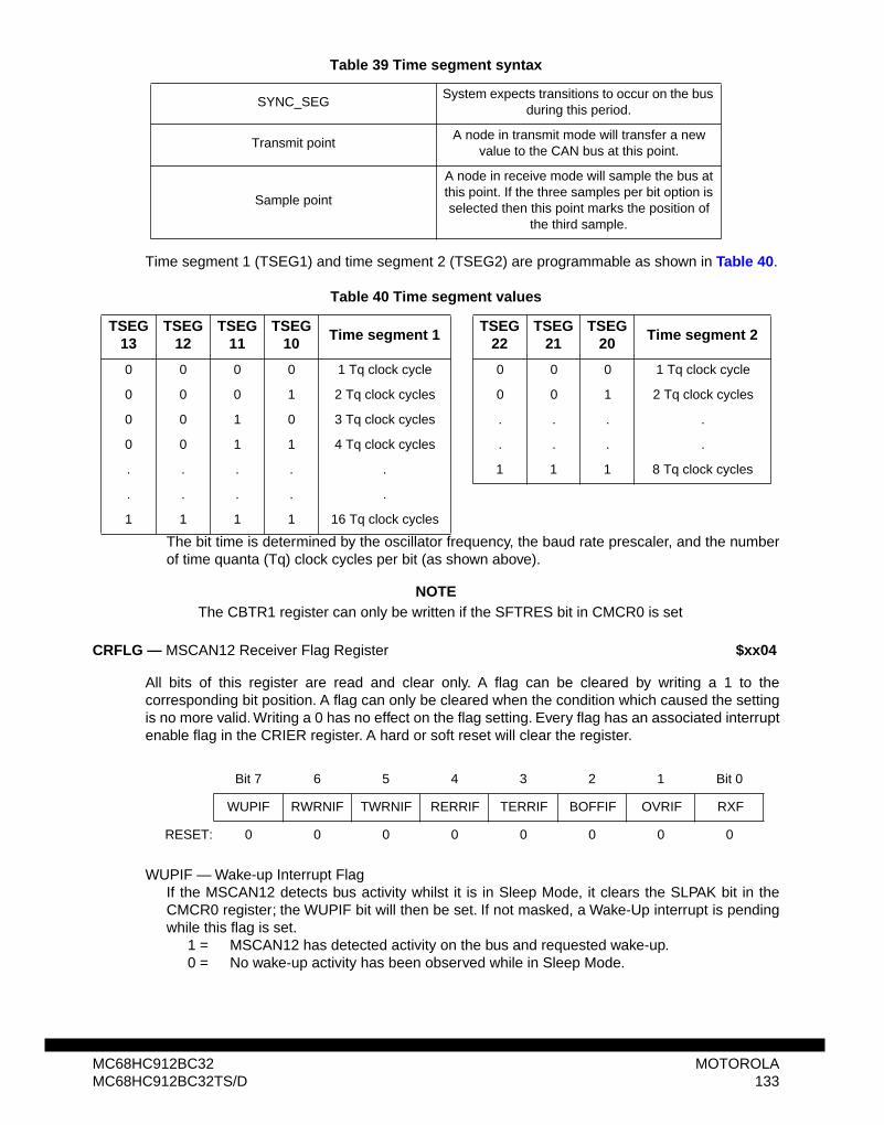
Time segment 1 (TSEG1) and time segment 2 (TSEG2) are programmable as shown in Table 40.
The bit time is determined by the oscillator frequency, the baud rate prescaler, and the numberof time quanta (Tq) clock cycles per bit (as shown above).
NOTEThe CBTR1 register can only be written if the SFTRES bit in CMCR0 is set
CRFLG — MSCAN12 Receiver Flag Register $xx04
All bits of this register are read and clear only. A flag can be cleared by writing a 1 to thecorresponding bit position. A flag can only be cleared when the condition which caused the settingis no more valid. Writing a 0 has no effect on the flag setting. Every flag has an associated interruptenable flag in the CRIER register. A hard or soft reset will clear the register.
WUPIF — Wake-up Interrupt FlagIf the MSCAN12 detects bus activity whilst it is in Sleep Mode, it clears the SLPAK bit in theCMCR0 register; the WUPIF bit will then be set. If not masked, a Wake-Up interrupt is pendingwhile this flag is set.
1 = MSCAN12 has detected activity on the bus and requested wake-up.0 = No wake-up activity has been observed while in Sleep Mode.
Table 39 Time segment syntax
SYNC_SEGSystem expects transitions to occur on the bus
during this period.
Transmit pointA node in transmit mode will transfer a new
value to the CAN bus at this point.
Sample point
A node in receive mode will sample the bus at this point. If the three samples per bit option is selected then this point marks the position of
the third sample.
Table 40 Time segment values
TSEG13
TSEG12
TSEG11
TSEG10
Time segment 1TSEG
22 TSEG
21TSEG
20Time segment 2
0 0 0 0 1 Tq clock cycle 0 0 0 1 Tq clock cycle
0 0 0 1 2 Tq clock cycles 0 0 1 2 Tq clock cycles
0 0 1 0 3 Tq clock cycles . . . .
0 0 1 1 4 Tq clock cycles . . . .
. . . . . 1 1 1 8 Tq clock cycles
. . . . .
1 1 1 1 16 Tq clock cycles
Bit 7 6 5 4 3 2 1 Bit 0
WUPIF RWRNIF TWRNIF RERRIF TERRIF BOFFIF OVRIF RXF
RESET: 0 0 0 0 0 0 0 0
MC68HC912BC32 MOTOROLAMC68HC912BC32TS/D 133
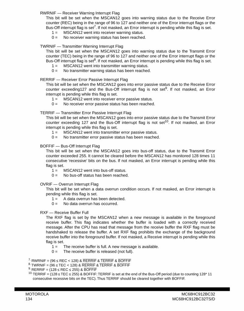
RWRNIF — Receiver Warning Interrupt FlagThis bit will be set when the MSCAN12 goes into warning status due to the Receive Errorcounter (REC) being in the range of 96 to 127 and neither one of the Error interrupt flags or theBus-Off interrupt flag is set7. If not masked, an Error interrupt is pending while this flag is set.
1 = MSCAN12 went into receiver warning status.0 = No receiver warning status has been reached.
TWRNIF — Transmitter Warning Interrupt FlagThis bit will be set when the MSCAN12 goes into warning status due to the Transmit Errorcounter (TEC) being in the range of 96 to 127 and neither one of the Error interrupt flags or theBus-Off interrupt flag is set8. If not masked, an Error interrupt is pending while this flag is set.
1 = MSCAN12 went into transmitter warning status.0 = No transmitter warning status has been reached.
RERRIF — Receiver Error Passive Interrupt FlagThis bit will be set when the MSCAN12 goes into error passive status due to the Receive Errorcounter exceeding127 and the Bus-Off interrupt flag is not set9. If not masked, an Errorinterrupt is pending while this flag is set.
1 = MSCAN12 went into receiver error passive status.0 = No receiver error passive status has been reached.
TERRIF — Transmitter Error Passive Interrupt FlagThis bit will be set when the MSCAN12 goes into error passive status due to the Transmit Errorcounter exceeding 127 and the Bus-Off interrupt flag is not set10. If not masked, an Errorinterrupt is pending while this flag is set.
1 = MSCAN12 went into transmitter error passive status.0 = No transmitter error passive status has been reached.
BOFFIF — Bus-Off Interrupt FlagThis bit will be set when the MSCAN12 goes into bus-off status, due to the Transmit Errorcounter exceeded 255. It cannot be cleared before the MSCAN12 has monitored 128 times 11consecutive ‘recessive’ bits on the bus. If not masked, an Error interrupt is pending while thisflag is set.
1 = MSCAN12 went into bus-off status.0 = No bus-off status has been reached.
OVRIF — Overrun Interrupt FlagThis bit will be set when a data overrun condition occurs. If not masked, an Error interrupt ispending while this flag is set.
1 = A data overrun has been detected.0 = No data overrun has occurred.
RXF — Receive Buffer FullThe RXF flag is set by the MSCAN12 when a new message is available in the foregroundreceive buffer. This flag indicates whether the buffer is loaded with a correctly receivedmessage. After the CPU has read that message from the receive buffer the RXF flag must behandshaked to release the buffer. A set RXF flag prohibits the exchange of the backgroundreceive buffer into the foreground buffer. If not masked, a Receive interrupt is pending while thisflag is set.
1 = The receive buffer is full. A new message is available.0 = The receive buffer is released (not full).
7. RWRNIF = (96 ≤ REC < 128) & RERRIF & TERRIF & BOFFIF8. TWRNIF = (96 ≤ TEC < 128) & RERRIF & TERRIF & BOFFIF9. RERRIF = (128 ≤ REC ≤ 255) & BOFFIF10. TERRIF = (128 ≤ TEC ≤ 255) & BOFFIF: TERRIF is set at the end of the Bus-Off period (due to counting 128* 11
MOTOROLA MC68HC912BC32134 MC68HC912BC32TS/D
consecutive recessive bits on the TEC). Thus TERRIF should be cleared together with BOFFIF.
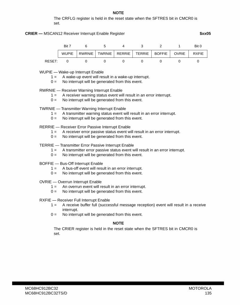
NOTEThe CRFLG register is held in the reset state when the SFTRES bit in CMCR0 isset.
CRIER — MSCAN12 Receiver Interrupt Enable Register $xx05
WUPIE — Wake-up Interrupt Enable1 = A wake-up event will result in a wake-up interrupt.0 = No interrupt will be generated from this event.
RWRNIE — Receiver Warning Interrupt Enable1 = A receiver warning status event will result in an error interrupt.0 = No interrupt will be generated from this event.
TWRNIE — Transmitter Warning Interrupt Enable1 = A transmitter warning status event will result in an error interrupt.0 = No interrupt will be generated from this event.
RERRIE — Receiver Error Passive Interrupt Enable1 = A receiver error passive status event will result in an error interrupt.0 = No interrupt will be generated from this event.
TERRIE — Transmitter Error Passive Interrupt Enable1 = A transmitter error passive status event will result in an error interrupt.0 = No interrupt will be generated from this event.
BOFFIE — Bus-Off Interrupt Enable1 = A bus-off event will result in an error interrupt.0 = No interrupt will be generated from this event.
OVRIE — Overrun Interrupt Enable1 = An overrun event will result in an error interrupt.0 = No interrupt will be generated from this event.
RXFIE — Receiver Full Interrupt Enable1 = A receive buffer full (successful message reception) event will result in a receive
interrupt.0 = No interrupt will be generated from this event.
NOTEThe CRIER register is held in the reset state when the SFTRES bit in CMCR0 isset.
Bit 7 6 5 4 3 2 1 Bit 0
WUPIE RWRNIE TWRNIE RERRIE TERRIE BOFFIE OVRIE RXFIE
RESET: 0 0 0 0 0 0 0 0
MC68HC912BC32 MOTOROLAMC68HC912BC32TS/D 135
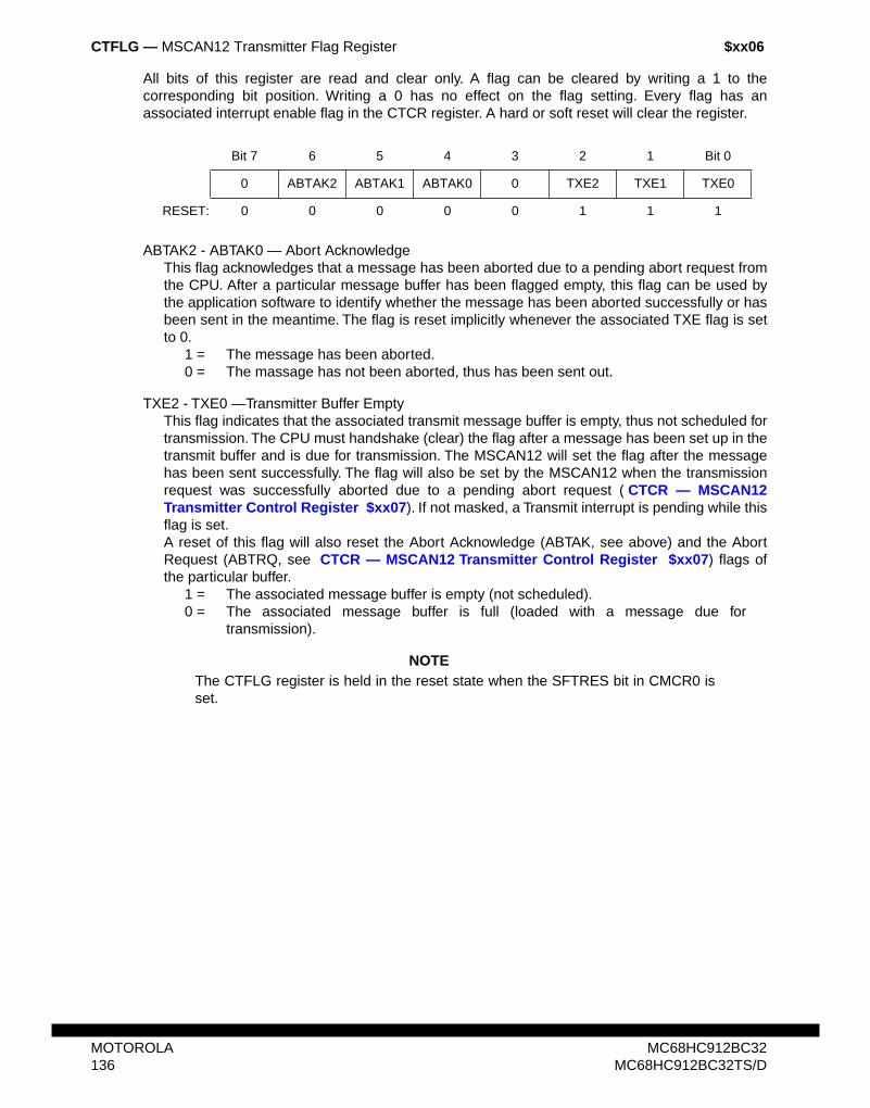
CTFLG — MSCAN12 Transmitter Flag Register $xx06
All bits of this register are read and clear only. A flag can be cleared by writing a 1 to thecorresponding bit position. Writing a 0 has no effect on the flag setting. Every flag has anassociated interrupt enable flag in the CTCR register. A hard or soft reset will clear the register.
ABTAK2 - ABTAK0 — Abort AcknowledgeThis flag acknowledges that a message has been aborted due to a pending abort request fromthe CPU. After a particular message buffer has been flagged empty, this flag can be used bythe application software to identify whether the message has been aborted successfully or hasbeen sent in the meantime. The flag is reset implicitly whenever the associated TXE flag is setto 0.
1 = The message has been aborted.0 = The massage has not been aborted, thus has been sent out.
TXE2 - TXE0 —Transmitter Buffer Empty This flag indicates that the associated transmit message buffer is empty, thus not scheduled fortransmission. The CPU must handshake (clear) the flag after a message has been set up in thetransmit buffer and is due for transmission. The MSCAN12 will set the flag after the messagehas been sent successfully. The flag will also be set by the MSCAN12 when the transmissionrequest was successfully aborted due to a pending abort request ( CTCR — MSCAN12Transmitter Control Register $xx07). If not masked, a Transmit interrupt is pending while thisflag is set.A reset of this flag will also reset the Abort Acknowledge (ABTAK, see above) and the AbortRequest (ABTRQ, see CTCR — MSCAN12 Transmitter Control Register $xx07) flags ofthe particular buffer.
1 = The associated message buffer is empty (not scheduled).0 = The associated message buffer is full (loaded with a message due for
transmission).
NOTEThe CTFLG register is held in the reset state when the SFTRES bit in CMCR0 isset.
Bit 7 6 5 4 3 2 1 Bit 0
0 ABTAK2 ABTAK1 ABTAK0 0 TXE2 TXE1 TXE0
RESET: 0 0 0 0 0 1 1 1
MOTOROLA MC68HC912BC32136 MC68HC912BC32TS/D
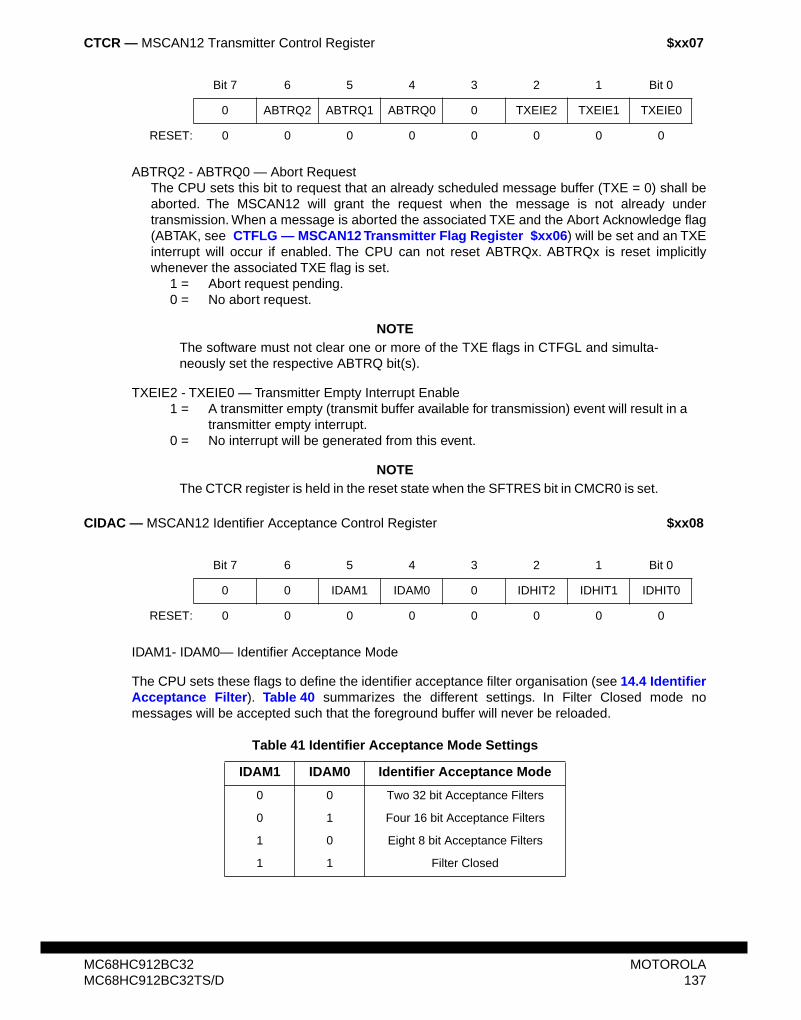
CTCR — MSCAN12 Transmitter Control Register $xx07
ABTRQ2 - ABTRQ0 — Abort RequestThe CPU sets this bit to request that an already scheduled message buffer (TXE = 0) shall beaborted. The MSCAN12 will grant the request when the message is not already undertransmission. When a message is aborted the associated TXE and the Abort Acknowledge flag(ABTAK, see CTFLG — MSCAN12 Transmitter Flag Register $xx06) will be set and an TXEinterrupt will occur if enabled. The CPU can not reset ABTRQx. ABTRQx is reset implicitlywhenever the associated TXE flag is set.
1 = Abort request pending.0 = No abort request.
NOTEThe software must not clear one or more of the TXE flags in CTFGL and simulta-neously set the respective ABTRQ bit(s).
TXEIE2 - TXEIE0 — Transmitter Empty Interrupt Enable1 = A transmitter empty (transmit buffer available for transmission) event will result in a
transmitter empty interrupt.0 = No interrupt will be generated from this event.
NOTEThe CTCR register is held in the reset state when the SFTRES bit in CMCR0 is set.
CIDAC — MSCAN12 Identifier Acceptance Control Register $xx08
IDAM1- IDAM0— Identifier Acceptance Mode
The CPU sets these flags to define the identifier acceptance filter organisation (see 14.4 IdentifierAcceptance Filter). Table 40 summarizes the different settings. In Filter Closed mode nomessages will be accepted such that the foreground buffer will never be reloaded.
Bit 7 6 5 4 3 2 1 Bit 0
0 ABTRQ2 ABTRQ1 ABTRQ0 0 TXEIE2 TXEIE1 TXEIE0
RESET: 0 0 0 0 0 0 0 0
Bit 7 6 5 4 3 2 1 Bit 0
0 0 IDAM1 IDAM0 0 IDHIT2 IDHIT1 IDHIT0
RESET: 0 0 0 0 0 0 0 0
Table 41 Identifier Acceptance Mode Settings
IDAM1 IDAM0 Identifier Acceptance Mode
0 0 Two 32 bit Acceptance Filters
0 1 Four 16 bit Acceptance Filters
1 0 Eight 8 bit Acceptance Filters
1 1 Filter Closed
MC68HC912BC32 MOTOROLAMC68HC912BC32TS/D 137
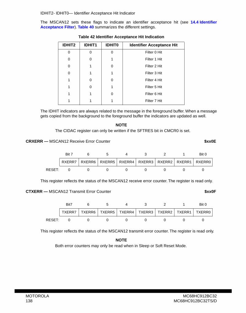
IDHIT2- IDHIT0— Identifier Acceptance Hit Indicator
The MSCAN12 sets these flags to indicate an identifier acceptance hit (see 14.4 IdentifierAcceptance Filter). Table 40 summarizes the different settings.
The IDHIT indicators are always related to the message in the foreground buffer. When a messagegets copied from the background to the foreground buffer the indicators are updated as well.
NOTEThe CIDAC register can only be written if the SFTRES bit in CMCR0 is set.
CRXERR — MSCAN12 Receive Error Counter $xx0E
This register reflects the status of the MSCAN12 receive error counter. The register is read only.
CTXERR — MSCAN12 Transmit Error Counter $xx0F
This register reflects the status of the MSCAN12 transmit error counter. The register is read only.
NOTEBoth error counters may only be read when in Sleep or Soft Reset Mode.
Table 42 Identifier Acceptance Hit Indication
IDHIT2 IDHIT1 IDHIT0 Identifier Acceptance Hit
0 0 0 Filter 0 Hit
0 0 1 Filter 1 Hit
0 1 0 Filter 2 Hit
0 1 1 Filter 3 Hit
1 0 0 Filter 4 Hit
1 0 1 Filter 5 Hit
1 1 0 Filter 6 Hit
1 1 1 Filter 7 Hit
Bit 7 6 5 4 3 2 1 Bit 0
RXERR7 RXERR6 RXERR5 RXERR4 RXERR3 RXERR2 RXERR1 RXERR0
RESET: 0 0 0 0 0 0 0 0
Bit7 6 5 4 3 2 1 Bit 0
TXERR7 TXERR6 TXERR5 TXERR4 TXERR3 TXERR2 TXERR1 TXERR0
RESET: 0 0 0 0 0 0 0 0
MOTOROLA MC68HC912BC32138 MC68HC912BC32TS/D
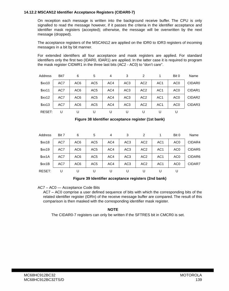
14.12.2 MSCAN12 Identifier Acceptance Registers (CIDAR0-7)
On reception each message is written into the background receive buffer. The CPU is onlysignalled to read the message however, if it passes the criteria in the identifier acceptance andidentifier mask registers (accepted); otherwise, the message will be overwritten by the nextmessage (dropped).
The acceptance registers of the MSCAN12 are applied on the IDR0 to IDR3 registers of incomingmessages in a bit by bit manner.
For extended identifiers all four acceptance and mask registers are applied. For standardidentifiers only the first two (IDAR0, IDAR1) are applied. In the latter case it is required to programthe mask register CIDMR1 in the three last bits (AC2 - AC0) to “don’t care”.
AC7 – AC0 — Acceptance Code BitsAC7 – AC0 comprise a user defined sequence of bits with which the corresponding bits of therelated identifier register (IDRn) of the receive message buffer are compared. The result of thiscomparison is then masked with the corresponding identifier mask register.
NOTEThe CIDAR0-7 registers can only be written if the SFTRES bit in CMCR0 is set.
Address Bit7 6 5 4 3 2 1 Bit 0 Name
$xx10 AC7 AC6 AC5 AC4 AC3 AC2 AC1 AC0 CIDAR0
$xx11 AC7 AC6 AC5 AC4 AC3 AC2 AC1 AC0 CIDAR1
$xx12 AC7 AC6 AC5 AC4 AC3 AC2 AC1 AC0 CIDAR2
$xx13 AC7 AC6 AC5 AC4 AC3 AC2 AC1 AC0 CIDAR3
RESET: U U U U U U U U
Figure 38 Identifier acceptance register (1st bank)
Address Bit 7 6 5 4 3 2 1 Bit 0 Name
$xx18 AC7 AC6 AC5 AC4 AC3 AC2 AC1 AC0 CIDAR4
$xx19 AC7 AC6 AC5 AC4 AC3 AC2 AC1 AC0 CIDAR5
$xx1A AC7 AC6 AC5 AC4 AC3 AC2 AC1 AC0 CIDAR6
$xx1B AC7 AC6 AC5 AC4 AC3 AC2 AC1 AC0 CIDAR7
RESET: U U U U U U U U
Figure 39 Identifier acceptance registers (2nd bank)
MC68HC912BC32 MOTOROLAMC68HC912BC32TS/D 139
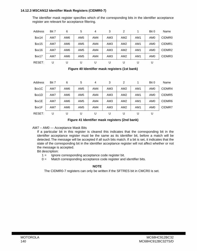
14.12.3 MSCAN12 Identifier Mask Registers (CIDMR0-7)
The identifier mask register specifies which of the corresponding bits in the identifier acceptanceregister are relevant for acceptance filtering.
AM7 – AM0 — Acceptance Mask BitsIf a particular bit in this register is cleared this indicates that the corresponding bit in theidentifier acceptance register must be the same as its identifier bit, before a match will bedetected. The message will be accepted if all such bits match. If a bit is set, it indicates that thestate of the corresponding bit in the identifier acceptance register will not affect whether or notthe message is accepted.Bit description:
1 = Ignore corresponding acceptance code register bit.0 = Match corresponding acceptance code register and identifier bits.
NOTEThe CIDMR0-7 registers can only be written if the SFTRES bit in CMCR0 is set.
Address Bit 7 6 5 4 3 2 1 Bit 0 Name
$xx14 AM7 AM6 AM5 AM4 AM3 AM2 AM1 AM0 CIDMR0
$xx15 AM7 AM6 AM5 AM4 AM3 AM2 AM1 AM0 CIDMR1
$xx16 AM7 AM6 AM5 AM4 AM3 AM2 AM1 AM0 CIDMR2
$xx17 AM7 AM6 AM5 AM4 AM3 AM2 AM1 AM0 CIDMR3
RESET: U U U U U U U U
Figure 40 Identifier mask registers (1st bank)
Address Bit 7 6 5 4 3 2 1 Bit 0 Name
$xx1C AM7 AM6 AM5 AM4 AM3 AM2 AM1 AM0 CIDMR4
$xx1D AM7 AM6 AM5 AM4 AM3 AM2 AM1 AM0 CIDMR5
$xx1E AM7 AM6 AM5 AM4 AM3 AM2 AM1 AM0 CIDMR6
$xx1F AM7 AM6 AM5 AM4 AM3 AM2 AM1 AM0 CIDMR7
RESET: U U U U U U U U
Figure 41 Identifier mask registers (2nd bank)
MOTOROLA MC68HC912BC32140 MC68HC912BC32TS/D
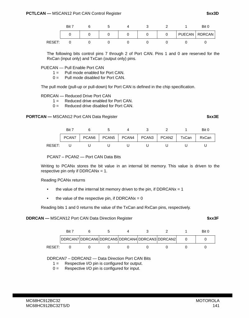
PCTLCAN — MSCAN12 Port CAN Control Register $xx3D
The following bits control pins 7 through 2 of Port CAN. Pins 1 and 0 are reserved for theRxCan (input only) and TxCan (output only) pins.
PUECAN — Pull Enable Port CAN1 = Pull mode enabled for Port CAN.0 = Pull mode disabled for Port CAN.
The pull mode (pull-up or pull-down) for Port CAN is defined in the chip specification.
RDRCAN — Reduced Drive Port CAN1 = Reduced drive enabled for Port CAN.0 = Reduced drive disabled for Port CAN.
PORTCAN — MSCAN12 Port CAN Data Register $xx3E
PCAN7 – PCAN2 — Port CAN Data Bits
Writing to PCANx stores the bit value in an internal bit memory. This value is driven to therespective pin only if DDRCANx = 1.
Reading PCANx returns
• the value of the internal bit memory driven to the pin, if DDRCANx = 1
• the value of the respective pin, if DDRCANx = 0
Reading bits 1 and 0 returns the value of the TxCan and RxCan pins, respectively.
DDRCAN — MSCAN12 Port CAN Data Direction Register $xx3F
DDRCAN7 – DDRCAN2 — Data Direction Port CAN Bits1 = Respective I/O pin is configured for output.0 = Respective I/O pin is configured for input.
Bit 7 6 5 4 3 2 1 Bit 0
0 0 0 0 0 0 PUECAN RDRCAN
RESET: 0 0 0 0 0 0 0 0
Bit 7 6 5 4 3 2 1 Bit 0
PCAN7 PCAN6 PCAN5 PCAN4 PCAN3 PCAN2 TxCan RxCan
RESET: U U U U U U U U
Bit 7 6 5 4 3 2 1 Bit 0
DDRCAN7 DDRCAN6 DDRCAN5 DDRCAN4 DDRCAN3 DDRCAN2 0 0
RESET: 0 0 0 0 0 0 0 0
MC68HC912BC32 MOTOROLAMC68HC912BC32TS/D 141

MOTOROLA MC68HC912BC32142 MC68HC912BC32TS/D
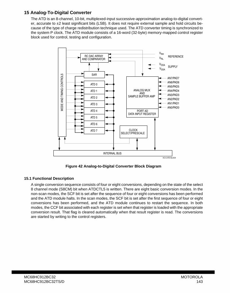
15 Analog-To-Digital ConverterThe ATD is an 8-channel, 10-bit, multiplexed-input successive-approximation analog-to-digital convert-er, accurate to ±2 least significant bits (LSB). It does not require external sample and hold circuits be-cause of the type of charge redistribution technique used. The ATD converter timing is synchronized tothe system P clock. The ATD module consists of a 16-word (32-byte) memory-mapped control registerblock used for control, testing and configuration.
Figure 42 Analog-to-Digital Converter Block Diagram
15.1 Functional Description
A single conversion sequence consists of four or eight conversions, depending on the state of the select8 channel mode (S8CM) bit when ATDCTL5 is written. There are eight basic conversion modes. In thenon-scan modes, the SCF bit is set after the sequence of four or eight conversions has been performedand the ATD module halts. In the scan modes, the SCF bit is set after the first sequence of four or eightconversions has been performed, and the ATD module continues to restart the sequence. In bothmodes, the CCF bit associated with each register is set when that register is loaded with the appropriateconversion result. That flag is cleared automatically when that result register is read. The conversionsare started by writing to the control registers.
MO
DE
AND
TIM
ING
CO
NTR
OLS
ATD 0
ATD 1
ATD 2
ATD 3
ATD 4
ATD 5
ATD 6
ATD 7
SAR
RC DAC ARRAYAND COMPARATOR
INTERNAL BUS
VDDA
VSSA
VRL
VRH
CLOCKSELECT/PRESCALE
ANALOG MUXAND
SAMPLE BUFFER AMP
PORT ADDATA INPUT REGISTER
AN7/PAD7AN6/PAD6AN5/PAD5AN4/PAD4AN3/PAD3AN2/PAD2AN1/PAD1AN0/PAD0
REFERENCE
SUPPLY
HC12 ATD BLOCK
MC68HC912BC32 MOTOROLAMC68HC912BC32TS/D 143
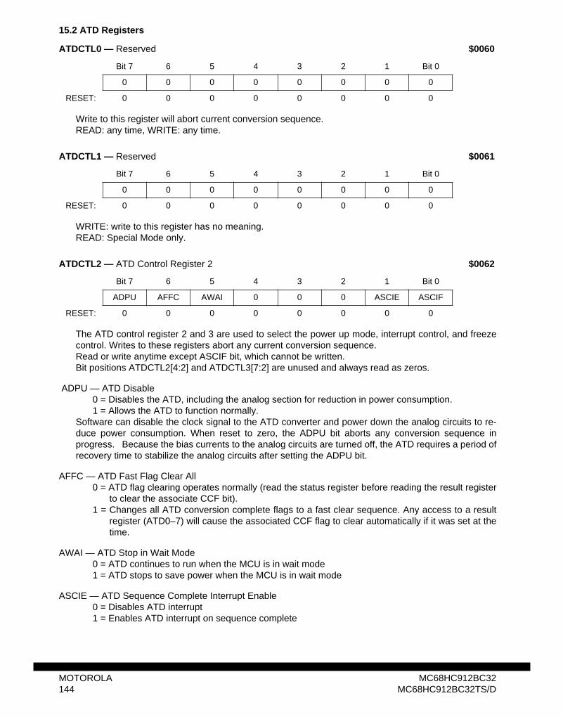
15.2 ATD Registers
Write to this register will abort current conversion sequence.READ: any time, WRITE: any time.
WRITE: write to this register has no meaning.READ: Special Mode only.
The ATD control register 2 and 3 are used to select the power up mode, interrupt control, and freezecontrol. Writes to these registers abort any current conversion sequence.Read or write anytime except ASCIF bit, which cannot be written.Bit positions ATDCTL2[4:2] and ATDCTL3[7:2] are unused and always read as zeros.
ADPU — ATD Disable0 = Disables the ATD, including the analog section for reduction in power consumption.1 = Allows the ATD to function normally.
Software can disable the clock signal to the ATD converter and power down the analog circuits to re-duce power consumption. When reset to zero, the ADPU bit aborts any conversion sequence inprogress. Because the bias currents to the analog circuits are turned off, the ATD requires a period ofrecovery time to stabilize the analog circuits after setting the ADPU bit.
AFFC — ATD Fast Flag Clear All 0 = ATD flag clearing operates normally (read the status register before reading the result register
to clear the associate CCF bit).1 = Changes all ATD conversion complete flags to a fast clear sequence. Any access to a result
register (ATD0–7) will cause the associated CCF flag to clear automatically if it was set at thetime.
AWAI — ATD Stop in Wait Mode0 = ATD continues to run when the MCU is in wait mode1 = ATD stops to save power when the MCU is in wait mode
ASCIE — ATD Sequence Complete Interrupt Enable 0 = Disables ATD interrupt1 = Enables ATD interrupt on sequence complete
ATDCTL0 — Reserved $0060
Bit 7 6 5 4 3 2 1 Bit 0
0 0 0 0 0 0 0 0
RESET: 0 0 0 0 0 0 0 0
ATDCTL1 — Reserved $0061
Bit 7 6 5 4 3 2 1 Bit 0
0 0 0 0 0 0 0 0
RESET: 0 0 0 0 0 0 0 0
ATDCTL2 — ATD Control Register 2 $0062
Bit 7 6 5 4 3 2 1 Bit 0
ADPU AFFC AWAI 0 0 0 ASCIE ASCIF
RESET: 0 0 0 0 0 0 0 0
MOTOROLA MC68HC912BC32144 MC68HC912BC32TS/D
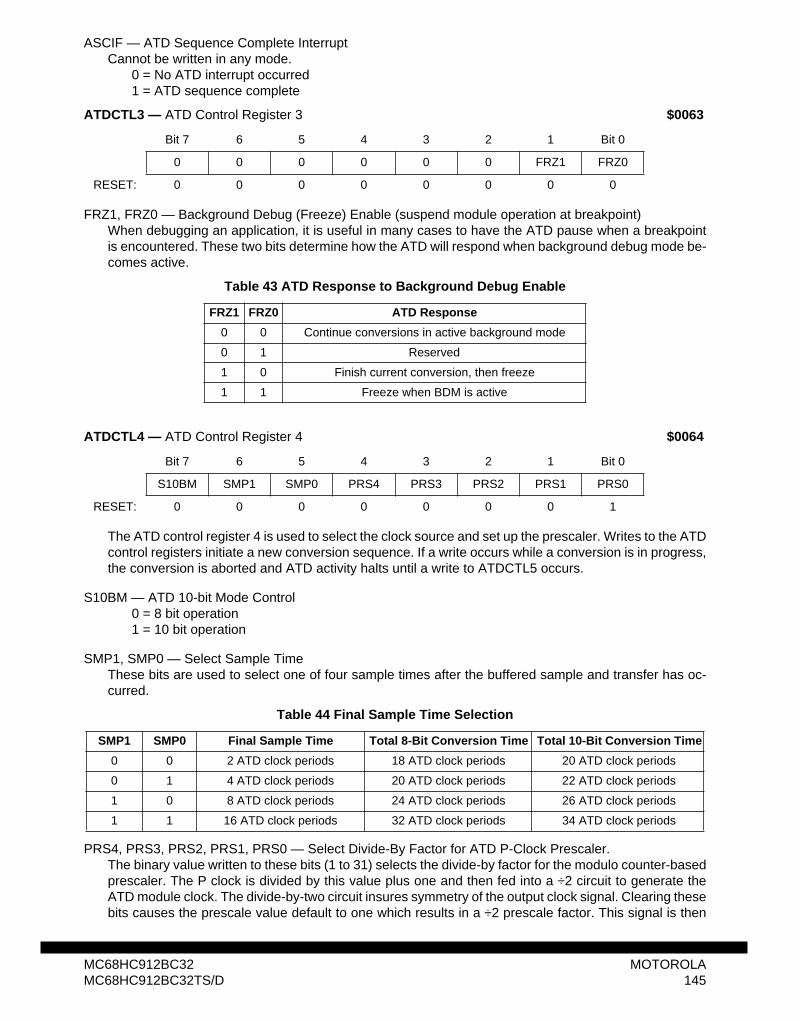
ASCIF — ATD Sequence Complete Interrupt Cannot be written in any mode.
0 = No ATD interrupt occurred1 = ATD sequence complete
FRZ1, FRZ0 — Background Debug (Freeze) Enable (suspend module operation at breakpoint)When debugging an application, it is useful in many cases to have the ATD pause when a breakpointis encountered. These two bits determine how the ATD will respond when background debug mode be-comes active.
The ATD control register 4 is used to select the clock source and set up the prescaler. Writes to the ATDcontrol registers initiate a new conversion sequence. If a write occurs while a conversion is in progress,the conversion is aborted and ATD activity halts until a write to ATDCTL5 occurs.
S10BM — ATD 10-bit Mode Control0 = 8 bit operation1 = 10 bit operation
SMP1, SMP0 — Select Sample TimeThese bits are used to select one of four sample times after the buffered sample and transfer has oc-curred.
PRS4, PRS3, PRS2, PRS1, PRS0 — Select Divide-By Factor for ATD P-Clock Prescaler.The binary value written to these bits (1 to 31) selects the divide-by factor for the modulo counter-basedprescaler. The P clock is divided by this value plus one and then fed into a ÷2 circuit to generate theATD module clock. The divide-by-two circuit insures symmetry of the output clock signal. Clearing these
ATDCTL3 — ATD Control Register 3 $0063
Bit 7 6 5 4 3 2 1 Bit 0
0 0 0 0 0 0 FRZ1 FRZ0
RESET: 0 0 0 0 0 0 0 0
Table 43 ATD Response to Background Debug Enable
FRZ1 FRZ0 ATD Response
0 0 Continue conversions in active background mode
0 1 Reserved
1 0 Finish current conversion, then freeze
1 1 Freeze when BDM is active
ATDCTL4 — ATD Control Register 4 $0064
Bit 7 6 5 4 3 2 1 Bit 0
S10BM SMP1 SMP0 PRS4 PRS3 PRS2 PRS1 PRS0
RESET: 0 0 0 0 0 0 0 1
Table 44 Final Sample Time Selection
SMP1 SMP0 Final Sample Time Total 8-Bit Conversion Time Total 10-Bit Conversion Time
0 0 2 ATD clock periods 18 ATD clock periods 20 ATD clock periods
0 1 4 ATD clock periods 20 ATD clock periods 22 ATD clock periods
1 0 8 ATD clock periods 24 ATD clock periods 26 ATD clock periods
1 1 16 ATD clock periods 32 ATD clock periods 34 ATD clock periods
MC68HC912BC32 MOTOROLAMC68HC912BC32TS/D 145
bits causes the prescale value default to one which results in a ÷2 prescale factor. This signal is then
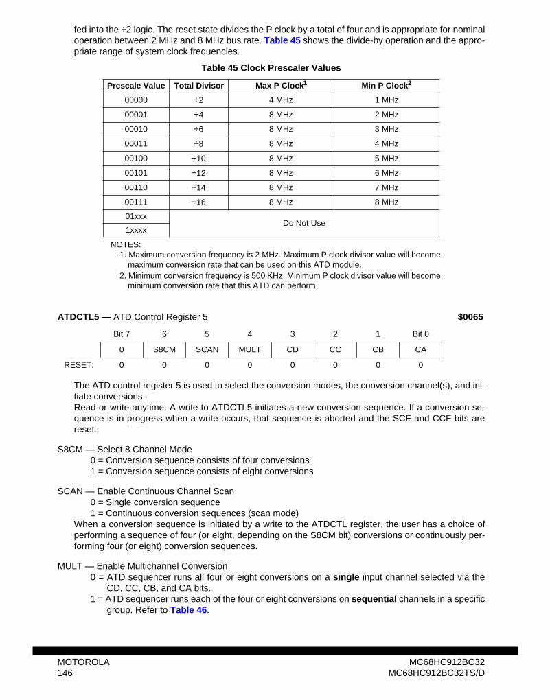
fed into the ÷2 logic. The reset state divides the P clock by a total of four and is appropriate for nominaloperation between 2 MHz and 8 MHz bus rate. Table 45 shows the divide-by operation and the appro-priate range of system clock frequencies.
The ATD control register 5 is used to select the conversion modes, the conversion channel(s), and ini-tiate conversions.Read or write anytime. A write to ATDCTL5 initiates a new conversion sequence. If a conversion se-quence is in progress when a write occurs, that sequence is aborted and the SCF and CCF bits arereset.
S8CM — Select 8 Channel Mode0 = Conversion sequence consists of four conversions1 = Conversion sequence consists of eight conversions
SCAN — Enable Continuous Channel Scan0 = Single conversion sequence1 = Continuous conversion sequences (scan mode)
When a conversion sequence is initiated by a write to the ATDCTL register, the user has a choice ofperforming a sequence of four (or eight, depending on the S8CM bit) conversions or continuously per-forming four (or eight) conversion sequences.
MULT — Enable Multichannel Conversion0 = ATD sequencer runs all four or eight conversions on a single input channel selected via the
CD, CC, CB, and CA bits.1 = ATD sequencer runs each of the four or eight conversions on sequential channels in a specific
group. Refer to Table 46.
NOTES:1. Maximum conversion frequency is 2 MHz. Maximum P clock divisor value will become
maximum conversion rate that can be used on this ATD module.2. Minimum conversion frequency is 500 KHz. Minimum P clock divisor value will become
minimum conversion rate that this ATD can perform.
Table 45 Clock Prescaler Values
Prescale Value Total Divisor Max P Clock1 Min P Clock2
00000 ÷2 4 MHz 1 MHz
00001 ÷4 8 MHz 2 MHz
00010 ÷6 8 MHz 3 MHz
00011 ÷8 8 MHz 4 MHz
00100 ÷10 8 MHz 5 MHz
00101 ÷12 8 MHz 6 MHz
00110 ÷14 8 MHz 7 MHz
00111 ÷16 8 MHz 8 MHz
01xxxDo Not Use
1xxxx
ATDCTL5 — ATD Control Register 5 $0065
Bit 7 6 5 4 3 2 1 Bit 0
0 S8CM SCAN MULT CD CC CB CA
RESET: 0 0 0 0 0 0 0 0
MOTOROLA MC68HC912BC32146 MC68HC912BC32TS/D
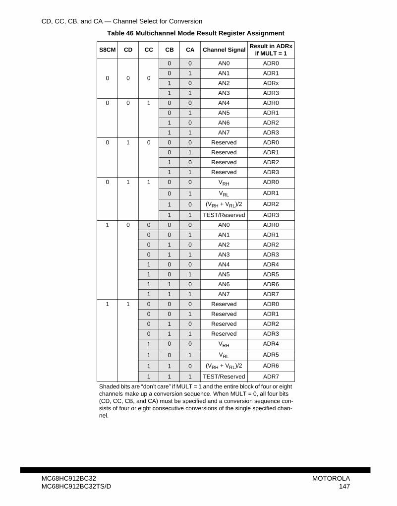
CD, CC, CB, and CA — Channel Select for Conversion
Table 46 Multichannel Mode Result Register Assignment
S8CM CD CC CB CA Channel SignalResult in ADRx
if MULT = 1
0 0 0
0 0 AN0 ADR0
0 1 AN1 ADR1
1 0 AN2 ADRx
1 1 AN3 ADR3
0 0 1 0 0 AN4 ADR0
0 1 AN5 ADR1
1 0 AN6 ADR2
1 1 AN7 ADR3
0 1 0 0 0 Reserved ADR0
0 1 Reserved ADR1
1 0 Reserved ADR2
1 1 Reserved ADR3
0 1 1 0 0 VRH ADR0
0 1 VRL ADR1
1 0 (VRH + VRL)/2 ADR2
1 1 TEST/Reserved ADR3
1 0 0 0 0 AN0 ADR0
0 0 1 AN1 ADR1
0 1 0 AN2 ADR2
0 1 1 AN3 ADR3
1 0 0 AN4 ADR4
1 0 1 AN5 ADR5
1 1 0 AN6 ADR6
1 1 1 AN7 ADR7
1 1 0 0 0 Reserved ADR0
0 0 1 Reserved ADR1
0 1 0 Reserved ADR2
0 1 1 Reserved ADR3
1 0 0 VRH ADR4
1 0 1 VRL ADR5
1 1 0 (VRH + VRL)/2 ADR6
1 1 1 TEST/Reserved ADR7
Shaded bits are “don’t care” if MULT = 1 and the entire block of four or eight channels make up a conversion sequence. When MULT = 0, all four bits (CD, CC, CB, and CA) must be specified and a conversion sequence con-sists of four or eight consecutive conversions of the single specified chan-nel.
MC68HC912BC32 MOTOROLAMC68HC912BC32TS/D 147
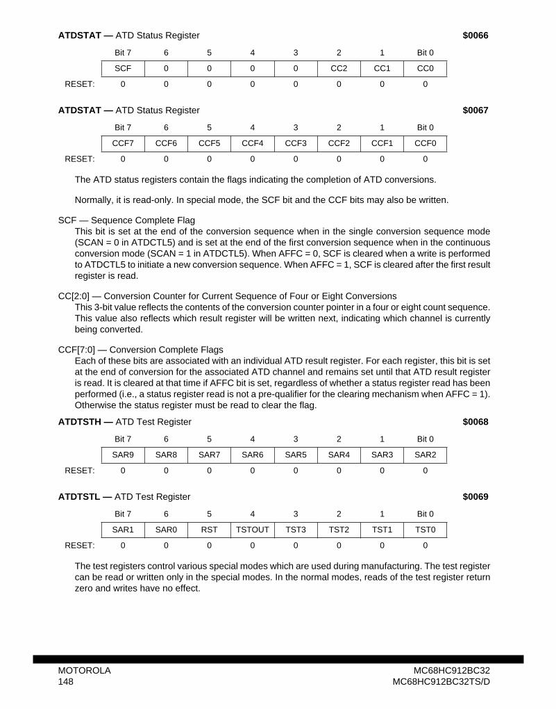
The ATD status registers contain the flags indicating the completion of ATD conversions.
Normally, it is read-only. In special mode, the SCF bit and the CCF bits may also be written.
SCF — Sequence Complete FlagThis bit is set at the end of the conversion sequence when in the single conversion sequence mode(SCAN = 0 in ATDCTL5) and is set at the end of the first conversion sequence when in the continuousconversion mode (SCAN = 1 in ATDCTL5). When AFFC = 0, SCF is cleared when a write is performedto ATDCTL5 to initiate a new conversion sequence. When AFFC = 1, SCF is cleared after the first resultregister is read.
CC[2:0] — Conversion Counter for Current Sequence of Four or Eight ConversionsThis 3-bit value reflects the contents of the conversion counter pointer in a four or eight count sequence.This value also reflects which result register will be written next, indicating which channel is currentlybeing converted.
CCF[7:0] — Conversion Complete FlagsEach of these bits are associated with an individual ATD result register. For each register, this bit is setat the end of conversion for the associated ATD channel and remains set until that ATD result registeris read. It is cleared at that time if AFFC bit is set, regardless of whether a status register read has beenperformed (i.e., a status register read is not a pre-qualifier for the clearing mechanism when AFFC = 1).Otherwise the status register must be read to clear the flag.
The test registers control various special modes which are used during manufacturing. The test registercan be read or written only in the special modes. In the normal modes, reads of the test register returnzero and writes have no effect.
ATDSTAT — ATD Status Register $0066
Bit 7 6 5 4 3 2 1 Bit 0
SCF 0 0 0 0 CC2 CC1 CC0
RESET: 0 0 0 0 0 0 0 0
ATDSTAT — ATD Status Register $0067
Bit 7 6 5 4 3 2 1 Bit 0
CCF7 CCF6 CCF5 CCF4 CCF3 CCF2 CCF1 CCF0
RESET: 0 0 0 0 0 0 0 0
ATDTSTH — ATD Test Register $0068
Bit 7 6 5 4 3 2 1 Bit 0
SAR9 SAR8 SAR7 SAR6 SAR5 SAR4 SAR3 SAR2
RESET: 0 0 0 0 0 0 0 0
ATDTSTL — ATD Test Register $0069
Bit 7 6 5 4 3 2 1 Bit 0
SAR1 SAR0 RST TSTOUT TST3 TST2 TST1 TST0
RESET: 0 0 0 0 0 0 0 0
MOTOROLA MC68HC912BC32148 MC68HC912BC32TS/D
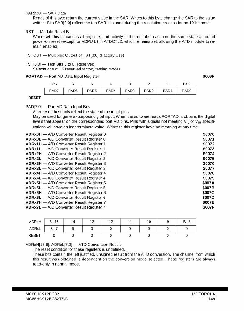
SAR[9:0] — SAR DataReads of this byte return the current value in the SAR. Writes to this byte change the SAR to the valuewritten. Bits SAR[9:0] reflect the ten SAR bits used during the resolution process for an 10-bit result.
RST — Module Reset BitWhen set, this bit causes all registers and activity in the module to assume the same state as out ofpower-on reset (except for ADPU bit in ATDCTL2, which remains set, allowing the ATD module to re-main enabled).
TSTOUT — Multiplex Output of TST[3:0] (Factory Use)
TST[3:0] — Test Bits 3 to 0 (Reserved)Selects one of 16 reserved factory testing modes
PAD[7:0] — Port AD Data Input BitsAfter reset these bits reflect the state of the input pins.May be used for general-purpose digital input. When the software reads PORTAD, it obtains the digitallevels that appear on the corresponding port AD pins. Pins with signals not meeting VIL or VIH specifi-cations will have an indeterminate value. Writes to this register have no meaning at any time.
ADRxH[15:8], ADRxL[7:0] — ATD Conversion ResultThe reset condition for these registers is undefined.These bits contain the left justified, unsigned result from the ATD conversion. The channel from whichthis result was obtained is dependent on the conversion mode selected. These registers are alwaysread-only in normal mode.
PORTAD — Port AD Data Input Register $006F
Bit 7 6 5 4 3 2 1 Bit 0
PAD7 PAD6 PAD5 PAD4 PAD3 PAD2 PAD1 PAD0
RESET: – – – – – – – –
ADRx0H — A/D Converter Result Register 0 $0070ADRx0L — A/D Converter Result Register 0 $0071ADRx1H — A/D Converter Result Register 1 $0072ADRx1L — A/D Converter Result Register 1 $0073ADRx2H — A/D Converter Result Register 2 $0074ADRx2L — A/D Converter Result Register 2 $0075ADRx3H — A/D Converter Result Register 3 $0076ADRx3L — A/D Converter Result Register 3 $0077ADRx4H — A/D Converter Result Register 4 $0078ADRx4L — A/D Converter Result Register 4 $0079ADRx5H — A/D Converter Result Register 5 $007AADRx5L — A/D Converter Result Register 5 $007BADRx6H — A/D Converter Result Register 6 $007CADRx6L — A/D Converter Result Register 6 $007DADRx7H — A/D Converter Result Register 7 $007EADRx7L — A/D Converter Result Register 7 $007F
ADRxH Bit 15 14 13 12 11 10 9 Bit 8
ADRxL Bit 7 6 0 0 0 0 0 0
RESET: 0 0 0 0 0 0 0 0
MC68HC912BC32 MOTOROLAMC68HC912BC32TS/D 149
15.3 ATD Mode Operation
STOP — causes all clocks to halt (if the S bit in the CCR is zero). The system is placed in a minimum-power standby mode. This aborts any conversion sequence in progress. During STOP recovery, theATD must delay for the STOP recovery time (tSR) before initiating a new ATD conversion sequence.
WAIT — ATD conversion continues unless AWAI bit in ATDCTL2 register is set.
BDM — Debug options available as set in register ATDCTL3.
USER — ATD continues running unless ADPU is cleared.
ADPU — ATD operations are stopped if ADPU = 0, but registers are accessible.
MOTOROLA MC68HC912BC32150 MC68HC912BC32TS/D
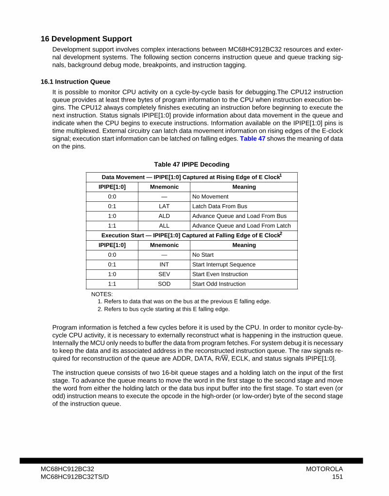
16 Development SupportDevelopment support involves complex interactions between MC68HC912BC32 resources and exter-nal development systems. The following section concerns instruction queue and queue tracking sig-nals, background debug mode, breakpoints, and instruction tagging.
16.1 Instruction Queue
It is possible to monitor CPU activity on a cycle-by-cycle basis for debugging.The CPU12 instructionqueue provides at least three bytes of program information to the CPU when instruction execution be-gins. The CPU12 always completely finishes executing an instruction before beginning to execute thenext instruction. Status signals IPIPE[1:0] provide information about data movement in the queue andindicate when the CPU begins to execute instructions. Information available on the IPIPE[1:0] pins istime multiplexed. External circuitry can latch data movement information on rising edges of the E-clocksignal; execution start information can be latched on falling edges. Table 47 shows the meaning of dataon the pins.
Program information is fetched a few cycles before it is used by the CPU. In order to monitor cycle-by-cycle CPU activity, it is necessary to externally reconstruct what is happening in the instruction queue.Internally the MCU only needs to buffer the data from program fetches. For system debug it is necessaryto keep the data and its associated address in the reconstructed instruction queue. The raw signals re-quired for reconstruction of the queue are ADDR, DATA, R/W, ECLK, and status signals IPIPE[1:0].
The instruction queue consists of two 16-bit queue stages and a holding latch on the input of the firststage. To advance the queue means to move the word in the first stage to the second stage and movethe word from either the holding latch or the data bus input buffer into the first stage. To start even (orodd) instruction means to execute the opcode in the high-order (or low-order) byte of the second stageof the instruction queue.
NOTES:1. Refers to data that was on the bus at the previous E falling edge.2. Refers to bus cycle starting at this E falling edge.
Table 47 IPIPE Decoding
Data Movement — IPIPE[1:0] Captured at Rising Edge of E Clock1
IPIPE[1:0] Mnemonic Meaning
0:0 — No Movement
0:1 LAT Latch Data From Bus
1:0 ALD Advance Queue and Load From Bus
1:1 ALL Advance Queue and Load From Latch
Execution Start — IPIPE[1:0] Captured at Falling Edge of E Clock2
IPIPE[1:0] Mnemonic Meaning
0:0 — No Start
0:1 INT Start Interrupt Sequence
1:0 SEV Start Even Instruction
1:1 SOD Start Odd Instruction
MC68HC912BC32 MOTOROLAMC68HC912BC32TS/D 151
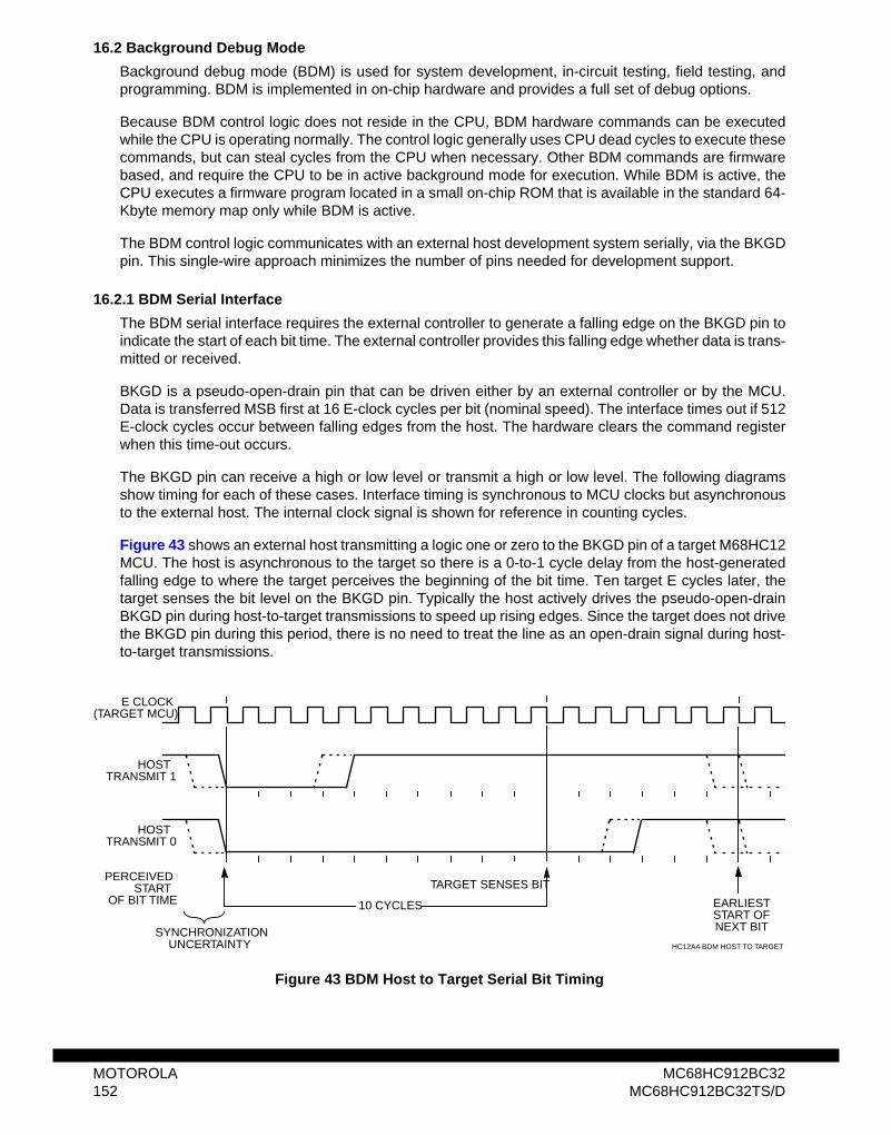
16.2 Background Debug Mode
Background debug mode (BDM) is used for system development, in-circuit testing, field testing, andprogramming. BDM is implemented in on-chip hardware and provides a full set of debug options.
Because BDM control logic does not reside in the CPU, BDM hardware commands can be executedwhile the CPU is operating normally. The control logic generally uses CPU dead cycles to execute thesecommands, but can steal cycles from the CPU when necessary. Other BDM commands are firmwarebased, and require the CPU to be in active background mode for execution. While BDM is active, theCPU executes a firmware program located in a small on-chip ROM that is available in the standard 64-Kbyte memory map only while BDM is active.
The BDM control logic communicates with an external host development system serially, via the BKGDpin. This single-wire approach minimizes the number of pins needed for development support.
16.2.1 BDM Serial Interface
The BDM serial interface requires the external controller to generate a falling edge on the BKGD pin toindicate the start of each bit time. The external controller provides this falling edge whether data is trans-mitted or received.
BKGD is a pseudo-open-drain pin that can be driven either by an external controller or by the MCU.Data is transferred MSB first at 16 E-clock cycles per bit (nominal speed). The interface times out if 512E-clock cycles occur between falling edges from the host. The hardware clears the command registerwhen this time-out occurs.
The BKGD pin can receive a high or low level or transmit a high or low level. The following diagramsshow timing for each of these cases. Interface timing is synchronous to MCU clocks but asynchronousto the external host. The internal clock signal is shown for reference in counting cycles.
Figure 43 shows an external host transmitting a logic one or zero to the BKGD pin of a target M68HC12MCU. The host is asynchronous to the target so there is a 0-to-1 cycle delay from the host-generatedfalling edge to where the target perceives the beginning of the bit time. Ten target E cycles later, thetarget senses the bit level on the BKGD pin. Typically the host actively drives the pseudo-open-drainBKGD pin during host-to-target transmissions to speed up rising edges. Since the target does not drivethe BKGD pin during this period, there is no need to treat the line as an open-drain signal during host-to-target transmissions.
Figure 43 BDM Host to Target Serial Bit Timing
HC12A4 BDM HOST TO TARGET T
EARLIESTSTART OFNEXT BIT
TARGET SENSES BIT
10 CYCLES
SYNCHRONIZATIONUNCERTAINTY
E CLOCK(TARGET MCU)
HOSTTRANSMIT 1
HOSTTRANSMIT 0
PERCEIVED START
OF BIT TIME
MOTOROLA MC68HC912BC32152 MC68HC912BC32TS/D
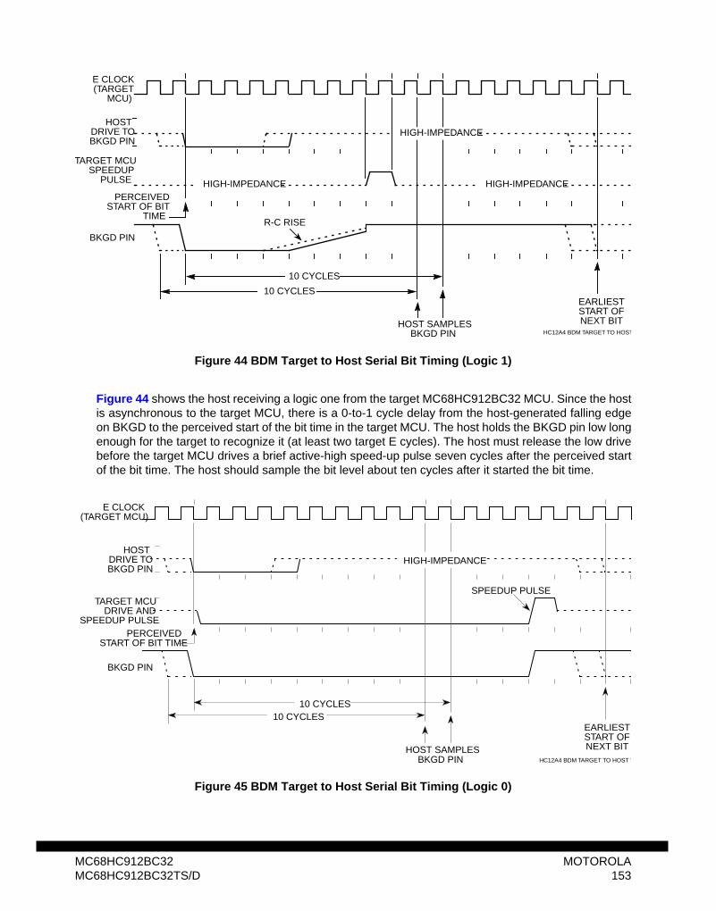
Figure 44 BDM Target to Host Serial Bit Timing (Logic 1)
Figure 44 shows the host receiving a logic one from the target MC68HC912BC32 MCU. Since the hostis asynchronous to the target MCU, there is a 0-to-1 cycle delay from the host-generated falling edgeon BKGD to the perceived start of the bit time in the target MCU. The host holds the BKGD pin low longenough for the target to recognize it (at least two target E cycles). The host must release the low drivebefore the target MCU drives a brief active-high speed-up pulse seven cycles after the perceived startof the bit time. The host should sample the bit level about ten cycles after it started the bit time.
Figure 45 BDM Target to Host Serial Bit Timing (Logic 0)
HC12A4 BDM TARGET TO HOST
HIGH-IMPEDANCE
HIGH-IMPEDANCE
HIGH-IMPEDANCE
EARLIESTSTART OFNEXT BIT
R-C RISE
10 CYCLES
10 CYCLES
HOST SAMPLESBKGD PIN
PERCEIVEDSTART OF BIT
TIME
BKGD PIN
E CLOCK(TARGET
MCU)
HOSTDRIVE TOBKGD PIN
TARGET MCUSPEEDUP
PULSE
HC12A4 BDM TARGET TO HOST T
EARLIESTSTART OFNEXT BIT
E CLOCK(TARGET MCU)
HOSTDRIVE TOBKGD PIN
BKGD PIN
PERCEIVEDSTART OF BIT TIME
10 CYCLES10 CYCLES
HOST SAMPLESBKGD PIN
TARGET MCUDRIVE AND
SPEEDUP PULSE
SPEEDUP PULSE
HIGH-IMPEDANCE
MC68HC912BC32 MOTOROLAMC68HC912BC32TS/D 153
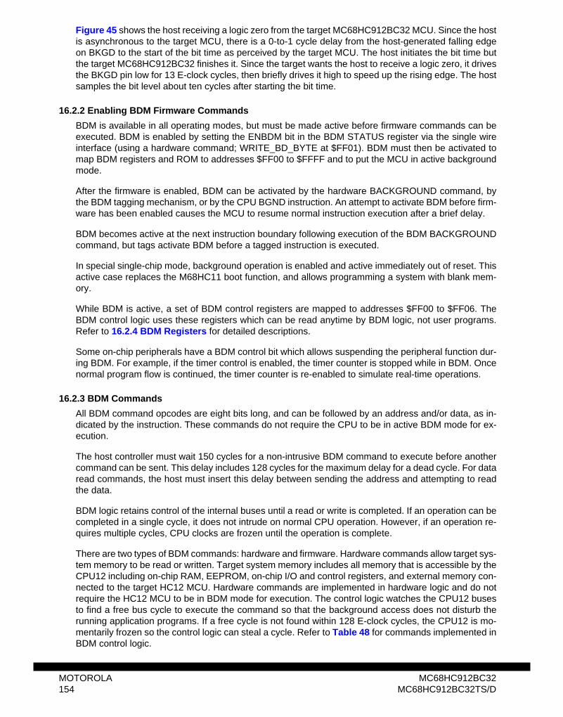
Figure 45 shows the host receiving a logic zero from the target MC68HC912BC32 MCU. Since the hostis asynchronous to the target MCU, there is a 0-to-1 cycle delay from the host-generated falling edgeon BKGD to the start of the bit time as perceived by the target MCU. The host initiates the bit time butthe target MC68HC912BC32 finishes it. Since the target wants the host to receive a logic zero, it drivesthe BKGD pin low for 13 E-clock cycles, then briefly drives it high to speed up the rising edge. The hostsamples the bit level about ten cycles after starting the bit time.
16.2.2 Enabling BDM Firmware Commands
BDM is available in all operating modes, but must be made active before firmware commands can beexecuted. BDM is enabled by setting the ENBDM bit in the BDM STATUS register via the single wireinterface (using a hardware command; WRITE_BD_BYTE at $FF01). BDM must then be activated tomap BDM registers and ROM to addresses $FF00 to $FFFF and to put the MCU in active backgroundmode.
After the firmware is enabled, BDM can be activated by the hardware BACKGROUND command, bythe BDM tagging mechanism, or by the CPU BGND instruction. An attempt to activate BDM before firm-ware has been enabled causes the MCU to resume normal instruction execution after a brief delay.
BDM becomes active at the next instruction boundary following execution of the BDM BACKGROUNDcommand, but tags activate BDM before a tagged instruction is executed.
In special single-chip mode, background operation is enabled and active immediately out of reset. Thisactive case replaces the M68HC11 boot function, and allows programming a system with blank mem-ory.
While BDM is active, a set of BDM control registers are mapped to addresses $FF00 to $FF06. TheBDM control logic uses these registers which can be read anytime by BDM logic, not user programs.Refer to 16.2.4 BDM Registers for detailed descriptions.
Some on-chip peripherals have a BDM control bit which allows suspending the peripheral function dur-ing BDM. For example, if the timer control is enabled, the timer counter is stopped while in BDM. Oncenormal program flow is continued, the timer counter is re-enabled to simulate real-time operations.
16.2.3 BDM Commands
All BDM command opcodes are eight bits long, and can be followed by an address and/or data, as in-dicated by the instruction. These commands do not require the CPU to be in active BDM mode for ex-ecution.
The host controller must wait 150 cycles for a non-intrusive BDM command to execute before anothercommand can be sent. This delay includes 128 cycles for the maximum delay for a dead cycle. For dataread commands, the host must insert this delay between sending the address and attempting to readthe data.
BDM logic retains control of the internal buses until a read or write is completed. If an operation can becompleted in a single cycle, it does not intrude on normal CPU operation. However, if an operation re-quires multiple cycles, CPU clocks are frozen until the operation is complete.
There are two types of BDM commands: hardware and firmware. Hardware commands allow target sys-tem memory to be read or written. Target system memory includes all memory that is accessible by theCPU12 including on-chip RAM, EEPROM, on-chip I/O and control registers, and external memory con-nected to the target HC12 MCU. Hardware commands are implemented in hardware logic and do notrequire the HC12 MCU to be in BDM mode for execution. The control logic watches the CPU12 busesto find a free bus cycle to execute the command so that the background access does not disturb therunning application programs. If a free cycle is not found within 128 E-clock cycles, the CPU12 is mo-
MOTOROLA MC68HC912BC32154 MC68HC912BC32TS/D
mentarily frozen so the control logic can steal a cycle. Refer to Table 48 for commands implemented inBDM control logic.
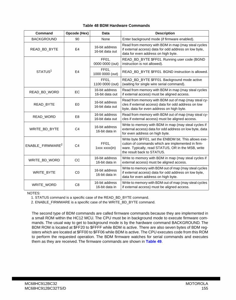
The second type of BDM commands are called firmware commands because they are implemented ina small ROM within the HC12 MCU. The CPU must be in background mode to execute firmware com-mands. The usual way to get to background mode is by the hardware command BACKGROUND. TheBDM ROM is located at $FF20 to $FFFF while BDM is active. There are also seven bytes of BDM reg-isters which are located at $FF00 to $FF06 while BDM is active. The CPU executes code from this ROMto perform the requested operation. The BDM firmware watches for serial commands and executesthem as they are received. The firmware commands are shown in Table 49.
NOTES:1. STATUS command is a specific case of the READ_BD_BYTE command.2. ENABLE_FIRMWARE is a specific case of the WRITE_BD_BYTE command.
Table 48 BDM Hardware Commands
Command Opcode (Hex) Data Description
BACKGROUND 90 None Enter background mode (if firmware enabled).
READ_BD_BYTE E416-bit address16-bit data out
Read from memory with BDM in map (may steal cycles if external access) data for odd address on low byte, data for even address on high byte.
STATUS1 E4
FF01, 0000 0000 (out)
READ_BD_BYTE $FF01. Running user code (BGND instruction is not allowed).
FF01,1000 0000 (out)
READ_BD_BYTE $FF01. BGND instruction is allowed.
FF01, 1100 0000 (out)
READ_BD_BYTE $FF01. Background mode active (waiting for single wire serial command).
READ_BD_WORD EC16-bit address 16-bit data out
Read from memory with BDM in map (may steal cycles if external access) must be aligned access.
READ_BYTE E016-bit address16-bit data out
Read from memory with BDM out of map (may steal cy-cles if external access) data for odd address on low byte, data for even address on high byte.
READ_WORD E816-bit address16-bit data out
Read from memory with BDM out of map (may steal cy-cles if external access) must be aligned access.
WRITE_BD_BYTE C416-bit address 16-bit data in
Write to memory with BDM in map (may steal cycles if external access) data for odd address on low byte, data for even address on high byte.
ENABLE_ FIRMWARE2 C4FF01,
1xxx xxxx(in)
Write byte $FF01, set the ENBDM bit. This allows exe-cution of commands which are implemented in firm-ware. Typically, read STATUS, OR in the MSB, write the result back to STATUS.
WRITE_BD_WORD CC16-bit address 16-bit data in
Write to memory with BDM in map (may steal cycles if external access) must be aligned access.
WRITE_BYTE C016-bit address 16-bit data in
Write to memory with BDM out of map (may steal cycles if external access) data for odd address on low byte, data for even address on high byte.
WRITE_WORD C816-bit address 16-bit data in
Write to memory with BDM out of map (may steal cycles if external access) must be aligned access.
MC68HC912BC32 MOTOROLAMC68HC912BC32TS/D 155
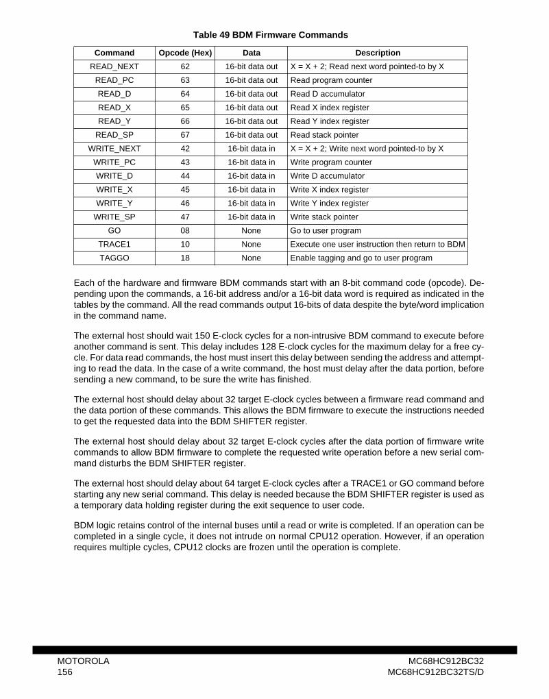
Each of the hardware and firmware BDM commands start with an 8-bit command code (opcode). De-pending upon the commands, a 16-bit address and/or a 16-bit data word is required as indicated in thetables by the command. All the read commands output 16-bits of data despite the byte/word implicationin the command name.
The external host should wait 150 E-clock cycles for a non-intrusive BDM command to execute beforeanother command is sent. This delay includes 128 E-clock cycles for the maximum delay for a free cy-cle. For data read commands, the host must insert this delay between sending the address and attempt-ing to read the data. In the case of a write command, the host must delay after the data portion, beforesending a new command, to be sure the write has finished.
The external host should delay about 32 target E-clock cycles between a firmware read command andthe data portion of these commands. This allows the BDM firmware to execute the instructions neededto get the requested data into the BDM SHIFTER register.
The external host should delay about 32 target E-clock cycles after the data portion of firmware writecommands to allow BDM firmware to complete the requested write operation before a new serial com-mand disturbs the BDM SHIFTER register.
The external host should delay about 64 target E-clock cycles after a TRACE1 or GO command beforestarting any new serial command. This delay is needed because the BDM SHIFTER register is used asa temporary data holding register during the exit sequence to user code.
BDM logic retains control of the internal buses until a read or write is completed. If an operation can becompleted in a single cycle, it does not intrude on normal CPU12 operation. However, if an operationrequires multiple cycles, CPU12 clocks are frozen until the operation is complete.
Table 49 BDM Firmware Commands
Command Opcode (Hex) Data Description
READ_NEXT 62 16-bit data out X = X + 2; Read next word pointed-to by X
READ_PC 63 16-bit data out Read program counter
READ_D 64 16-bit data out Read D accumulator
READ_X 65 16-bit data out Read X index register
READ_Y 66 16-bit data out Read Y index register
READ_SP 67 16-bit data out Read stack pointer
WRITE_NEXT 42 16-bit data in X = X + 2; Write next word pointed-to by X
WRITE_PC 43 16-bit data in Write program counter
WRITE_D 44 16-bit data in Write D accumulator
WRITE_X 45 16-bit data in Write X index register
WRITE_Y 46 16-bit data in Write Y index register
WRITE_SP 47 16-bit data in Write stack pointer
GO 08 None Go to user program
TRACE1 10 None Execute one user instruction then return to BDM
TAGGO 18 None Enable tagging and go to user program
MOTOROLA MC68HC912BC32156 MC68HC912BC32TS/D
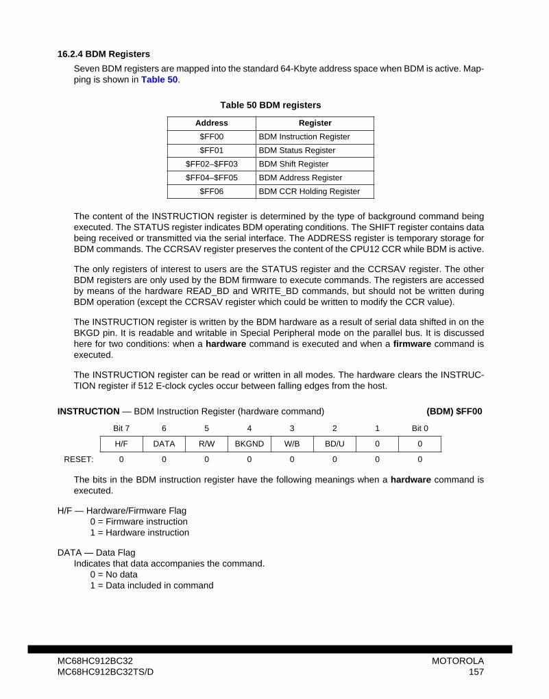
16.2.4 BDM Registers
Seven BDM registers are mapped into the standard 64-Kbyte address space when BDM is active. Map-ping is shown in Table 50.
The content of the INSTRUCTION register is determined by the type of background command beingexecuted. The STATUS register indicates BDM operating conditions. The SHIFT register contains databeing received or transmitted via the serial interface. The ADDRESS register is temporary storage forBDM commands. The CCRSAV register preserves the content of the CPU12 CCR while BDM is active.
The only registers of interest to users are the STATUS register and the CCRSAV register. The otherBDM registers are only used by the BDM firmware to execute commands. The registers are accessedby means of the hardware READ_BD and WRITE_BD commands, but should not be written duringBDM operation (except the CCRSAV register which could be written to modify the CCR value).
The INSTRUCTION register is written by the BDM hardware as a result of serial data shifted in on theBKGD pin. It is readable and writable in Special Peripheral mode on the parallel bus. It is discussedhere for two conditions: when a hardware command is executed and when a firmware command isexecuted.
The INSTRUCTION register can be read or written in all modes. The hardware clears the INSTRUC-TION register if 512 E-clock cycles occur between falling edges from the host.
The bits in the BDM instruction register have the following meanings when a hardware command isexecuted.
H/F — Hardware/Firmware Flag0 = Firmware instruction1 = Hardware instruction
DATA — Data FlagIndicates that data accompanies the command.
0 = No data1 = Data included in command
Table 50 BDM registers
Address Register
$FF00 BDM Instruction Register
$FF01 BDM Status Register
$FF02–$FF03 BDM Shift Register
$FF04–$FF05 BDM Address Register
$FF06 BDM CCR Holding Register
INSTRUCTION — BDM Instruction Register (hardware command) (BDM) $FF00
Bit 7 6 5 4 3 2 1 Bit 0
H/F DATA R/W BKGND W/B BD/U 0 0
RESET: 0 0 0 0 0 0 0 0
MC68HC912BC32 MOTOROLAMC68HC912BC32TS/D 157
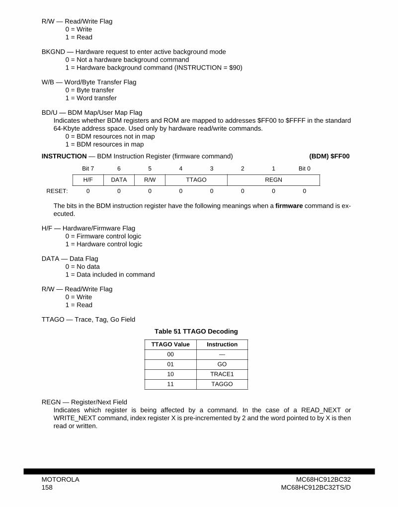
R/W — Read/Write Flag0 = Write1 = Read
BKGND — Hardware request to enter active background mode0 = Not a hardware background command1 = Hardware background command (INSTRUCTION = $90)
W/B — Word/Byte Transfer Flag0 = Byte transfer1 = Word transfer
BD/U — BDM Map/User Map FlagIndicates whether BDM registers and ROM are mapped to addresses $FF00 to $FFFF in the standard64-Kbyte address space. Used only by hardware read/write commands.
0 = BDM resources not in map1 = BDM resources in map
The bits in the BDM instruction register have the following meanings when a firmware command is ex-ecuted.
H/F — Hardware/Firmware Flag0 = Firmware control logic1 = Hardware control logic
DATA — Data Flag0 = No data1 = Data included in command
R/W — Read/Write Flag0 = Write1 = Read
TTAGO — Trace, Tag, Go Field
REGN — Register/Next FieldIndicates which register is being affected by a command. In the case of a READ_NEXT orWRITE_NEXT command, index register X is pre-incremented by 2 and the word pointed to by X is thenread or written.
INSTRUCTION — BDM Instruction Register (firmware command) (BDM) $FF00
Bit 7 6 5 4 3 2 1 Bit 0
H/F DATA R/W TTAGO REGN
RESET: 0 0 0 0 0 0 0 0
Table 51 TTAGO Decoding
TTAGO Value Instruction
00 —
01 GO
10 TRACE1
11 TAGGO
MOTOROLA MC68HC912BC32158 MC68HC912BC32TS/D
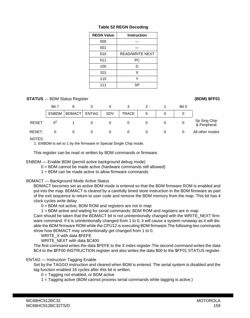
This register can be read or written by BDM commands or firmware.
ENBDM — Enable BDM (permit active background debug mode)0 = BDM cannot be made active (hardware commands still allowed)1 = BDM can be made active to allow firmware commands
BDMACT — Background Mode Active StatusBDMACT becomes set as active BDM mode is entered so that the BDM firmware ROM is enabled andput into the map. BDMACT is cleared by a carefully timed store instruction in the BDM firmware as partof the exit sequence to return to user code and remove the BDM memory from the map. This bit has 4clock cycles write delay.
0 = BDM not active; BDM ROM and registers are not in map1 = BDM active and waiting for serial commands; BDM ROM and registers are in map
Care should be taken that the BDMACT bit is not unintentionally changed with the WRITE_NEXT firm-ware command. If it is unintentionally changed from 1 to 0, it will cause a system runaway as it will dis-able the BDM firmware ROM while the CPU12 is executing BDM firmware.The following two commandsshow how BDMACT may unintentionally get changed from 1 to 0.
WRITE_X with data $FEFEWRITE_NEXT with data $C400
The first command writes the data $FEFE to the X index register.The second command writes the data$C4 to the $FF00 INSTRUCTION register and also writes the data $00 to the $FF01 STATUS register.
ENTAG — Instruction Tagging EnableSet by the TAGGO instruction and cleared when BDM is entered. The serial system is disabled and thetag function enabled 16 cycles after this bit is written.
0 = Tagging not enabled, or BDM active
NOTES:1. ENBDM is set to 1 by the firmware in Special Single Chip mode.
Table 52 REGN Decoding
REGN Value Instruction
000 —
001 —
010 READ/WRITE NEXT
011 PC
100 D
101 X
110 Y
111 SP
STATUS — BDM Status Register (BDM) $FF01
Bit 7 6 5 4 3 2 1 Bit 0
ENBDM BDMACT ENTAG SDV TRACE 0 0 0
RESET 01 1 0 0 0 0 0 0 Sp Sing Chip & Peripheral
RESET: 0 0 0 0 0 0 0 0 All other modes
MC68HC912BC32 MOTOROLAMC68HC912BC32TS/D 159
1 = Tagging active (BDM cannot process serial commands while tagging is active.)
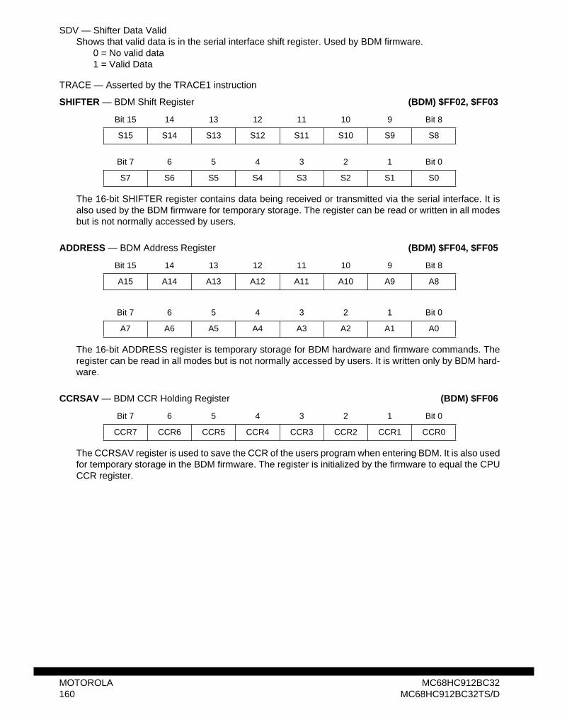
SDV — Shifter Data ValidShows that valid data is in the serial interface shift register. Used by BDM firmware.
0 = No valid data1 = Valid Data
TRACE — Asserted by the TRACE1 instruction
The 16-bit SHIFTER register contains data being received or transmitted via the serial interface. It isalso used by the BDM firmware for temporary storage. The register can be read or written in all modesbut is not normally accessed by users.
The 16-bit ADDRESS register is temporary storage for BDM hardware and firmware commands. Theregister can be read in all modes but is not normally accessed by users. It is written only by BDM hard-ware.
The CCRSAV register is used to save the CCR of the users program when entering BDM. It is also usedfor temporary storage in the BDM firmware. The register is initialized by the firmware to equal the CPUCCR register.
SHIFTER — BDM Shift Register (BDM) $FF02, $FF03
Bit 15 14 13 12 11 10 9 Bit 8
S15 S14 S13 S12 S11 S10 S9 S8
Bit 7 6 5 4 3 2 1 Bit 0
S7 S6 S5 S4 S3 S2 S1 S0
ADDRESS — BDM Address Register (BDM) $FF04, $FF05
Bit 15 14 13 12 11 10 9 Bit 8
A15 A14 A13 A12 A11 A10 A9 A8
Bit 7 6 5 4 3 2 1 Bit 0
A7 A6 A5 A4 A3 A2 A1 A0
CCRSAV — BDM CCR Holding Register (BDM) $FF06
Bit 7 6 5 4 3 2 1 Bit 0
CCR7 CCR6 CCR5 CCR4 CCR3 CCR2 CCR1 CCR0
MOTOROLA MC68HC912BC32160 MC68HC912BC32TS/D
16.3 Breakpoints
Hardware breakpoints are used to debug software on the MC68HC912BC32 by comparing actual ad-dress and data values to predetermined data in setup registers. A successful comparison will place theCPU in background debug mode (BDM) or initiate a software interrupt (SWI). Breakpoint features de-signed into the MC68HC912B32 include:
• Mode selection for BDM or SWI generation• Program fetch tagging for cycle of execution breakpoint• Second address compare in dual address modes• Range compare by disable of low byte address• Data compare in full feature mode for non-tagged breakpoint• Byte masking for high/low byte data compares• R/W compare for non-tagged compares• Tag inhibit on BDM TRACE
16.3.1 Breakpoint Modes
Three modes of operation determine the type of breakpoint in effect.
• Dual address-only breakpoints, each of which will cause a software interrupt (SWI)• Single full-feature breakpoint which will cause the part to enter background debug mode (BDM)• Dual address-only breakpoints, each of which will cause the part to enter BDM
Breakpoints will not occur when BDM is active.
16.3.1.1 SWI Dual Address Mode
In this mode, dual address-only breakpoints can be set, each of which cause a software interrupt. Thisis the only breakpoint mode which can force the CPU to execute a SWI. Program fetch tagging is thedefault in this mode; data breakpoints are not possible. In the dual mode each address breakpoint isaffected by the respective BKALE bit. The BKxRW, BKxRWE, BKMBH and BKMBL bits are ignored. Indual address mode the BKDBE becomes an enable for the second address breakpoint.
16.3.1.2 BDM Full Breakpoint Mode
This is a single full-featured breakpoint which causes the part to enter background debug mode.BK1ALE, BK1RW, and BK1RWE have no meaning in full breakpoint mode.
BKDBE enables data compare but has no meaning if BKPM=1. BKMBH and BKMBL allow masking ofhigh and low byte compares but has no meaning if BKPM=1. BK0ALE enables compare of low addressbyte.
• Breakpoints are not allowed if the BDM mode is already active. Active mode means the CPU isexecuting out of the BDM ROM.
• BDM should not be entered from a breakpoint unless the ENABLE bit is set in the BDM. This isimportant because even if the ENABLE bit in the BDM is negated the CPU actually does executethe BDM ROM code. It checks the ENABLE and returns if not set. If the BDM is not serviced bythe monitor then the breakpoint would be re-asserted when the BDM returns to normal CPU flow.There is no hardware to enforce restriction of breakpoint operation if the BDM is not enabled.
MC68HC912BC32 MOTOROLAMC68HC912BC32TS/D 161
16.3.1.3 BDM Dual Address Mode
Dual address-only breakpoints, each of which cause the part to enter background debug mode. In thedual mode each address breakpoint is affected by the BKPM bit, the BKxALE bits, and the BKxRW andBKxRWE bits. In dual address mode the BKDBE becomes an enable for the second address break-point. The BKMBH and BKMBL bits will have no effect when in a dual address mode. BDM mode maybe entered by a breakpoint only if an internal signal from the BDM indicates background debug modeis enabled. If BKPM = 1 then BKxRW, BKxRWE, BKMBH and BKMBL have no meaning.
• Breakpoints are not allowed if the BDM mode is already active. Active mode means the CPU isexecuting out of the BDM ROM.
• BDM should not be entered from a breakpoint unless the ENABLE bit is set in the BDM. This isimportant because even if the ENABLE bit in the BDM is negated the CPU actually does executethe BDM ROM code. It checks the ENABLE and returns if not set. If the BDM is not serviced bythe monitor then the breakpoint would be re-asserted when the BDM returns to normal CPU flow.There is no hardware to enforce restriction of breakpoint operation if the BDM is not enabled.
16.3.2 Registers
Breakpoint operation consists of comparing data in the breakpoint address registers (BRKAH/BRKAL)to the address bus and comparing data in the breakpoint data registers (BRKDH/BRKDL) to the databus. The breakpoint data registers can also be compared to the address bus. The scope of comparisoncan be expanded by ignoring the least significant byte of address or data matches.
The scope of comparison can be limited to program data only by setting the BKPM bit in breakpoint con-trol register 0.
To trace program flow, setting the BKPM bit causes address comparison of program data only. Controlbits are also available that allow checking read/write matches.
Read and write anytime.This register is used to control the breakpoint logic.
BKEN1, BKEN0 — Breakpoint Mode Enable
BRKCT0 — Breakpoint Control Register 0 $0020
Bit 7 6 5 4 3 2 1 Bit 0
BKEN1 BKEN0 BKPM 0 BK1ALE BK0ALE 0 0
RESET: 0 0 0 0 0 0 0 0
Table 53 Breakpoint Mode Control
BKEN1 BKEN0 Mode Selected BRKAH/L Usage BRKDH/L Usage R/W Range
0 0 Breakpoints Off — — — —
0 1 SWI — Dual Address Mode Address Match Address Match No Yes
1 0 BDM — Full Breakpoint Mode Address Match Data Match Yes Yes
1 1 BDM — Dual Address Mode Address Match Address Match Yes Yes
MOTOROLA MC68HC912BC32162 MC68HC912BC32TS/D
BKPM — Break on Program AddressesThis bit controls whether the breakpoint will cause an immediate data breakpoint (next instructionboundary) or a delayed program breakpoint related to an executable opcode. Data and unexecuted op-codes cannot cause a break if this bit is set. This bit has no meaning in SWI dual address mode. TheSWI mode only performs program breakpoints.
0 = On match, break at the next instruction boundary1 = On match, break if the match is an instruction that will be executed. This uses tagging as its
breakpoint mechanism.
BK1ALE — Breakpoint 1 Range ControlOnly valid in dual address mode.
0 = BRKDL will not be used to compare to the address bus.1 = BRKDL will be used to compare to the address bus.
BK0ALE — Breakpoint 0 Range ControlValid in all modes.
0 = BRKAL will not be used to compare to the address bus.1 = BRKAL will be used to compare to the address bus.
This register is read/write in all modes.
BKDBE — Enable Data BusEnables comparing of address or data bus values using the BRKDH/L registers.
0 = BRKDH/L registers are not used in any comparison1 = BRKDH/L registers are used to compare address or data (depending upon the mode selections
BKEN1,0)
BKMBH — Breakpoint Mask HighDisables the comparing of the high byte of data when in full breakpoint mode. Used in conjunction withthe BKDBE bit (which should be set)
0 = High byte of data bus (bits 15:8) are compared to BRKDH1 = High byte is not used to in comparisons
BKMBL — Breakpoint Mask LowDisables the matching of the low byte of data when in full breakpoint mode. Used in conjunction withthe BKDBE bit (which should be set)
0 = Low byte of data bus (bits 7:0) are compared to BRKDL
Table 54 Breakpoint Address Range Control
BK1ALE BK0ALE Address Range Selected
– 0 Upper 8-bit address only for full mode or dual mode BKP0
– 1 Full 16-bit address for full mode or dual mode BKP0
0 – Upper 8-bit address only for dual mode BKP1
1 – Full 16-bit address for dual mode BKP1
BRKCT1 — Breakpoint Control Register 1 $0021
Bit 7 6 5 4 3 2 1 Bit 0
0 BKDBE BKMBH BKMBL BK1RWE BK1RW BK0RWE BK0RW
RESET: 0 0 0 0 0 0 0 0
MC68HC912BC32 MOTOROLAMC68HC912BC32TS/D 163
1 = Low byte is not used to in comparisons.
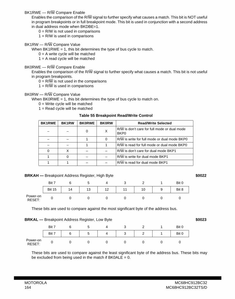
BK1RWE — R/W Compare EnableEnables the comparison of the R/W signal to further specify what causes a match. This bit is NOT usefulin program breakpoints or in full breakpoint mode. This bit is used in conjunction with a second addressin dual address mode when BKDBE=1.
0 = R/W is not used in comparisons1 = R/W is used in comparisons
BK1RW — R/W Compare ValueWhen BK1RWE = 1, this bit determines the type of bus cycle to match.
0 = A write cycle will be matched1 = A read cycle will be matched
BK0RWE — R/W Compare EnableEnables the comparison of the R/W signal to further specify what causes a match. This bit is not usefulin program breakpoints.
0 = R/W is not used in the comparisons1 = R/W is used in comparisons
BK0RW — R/W Compare ValueWhen BK0RWE = 1, this bit determines the type of bus cycle to match on.
0 = Write cycle will be matched1 = Read cycle will be matched
These bits are used to compare against the most significant byte of the address bus.
These bits are used to compare against the least significant byte of the address bus. These bits maybe excluded from being used in the match if BK0ALE = 0.
Table 55 Breakpoint Read/Write Control
BK1RWE BK1RW BK0RWE BK0RW Read/Write Selected
– – 0 XR/W is don’t care for full mode or dual mode BKP0
– – 1 0 R/W is write for full mode or dual mode BKP0
– – 1 1 R/W is read for full mode or dual mode BKP0
0 X – – R/W is don’t care for dual mode BKP1
1 0 – – R/W is write for dual mode BKP1
1 1 – – R/W is read for dual mode BKP1
BRKAH — Breakpoint Address Register, High Byte $0022
Bit 7 6 5 4 3 2 1 Bit 0
Bit 15 14 13 12 11 10 9 Bit 8
Power-on RESET: 0 0 0 0 0 0 0 0
BRKAL — Breakpoint Address Register, Low Byte $0023
Bit 7 6 5 4 3 2 1 Bit 0
Bit 7 6 5 4 3 2 1 Bit 0
Power-on RESET: 0 0 0 0 0 0 0 0
MOTOROLA MC68HC912BC32164 MC68HC912BC32TS/D
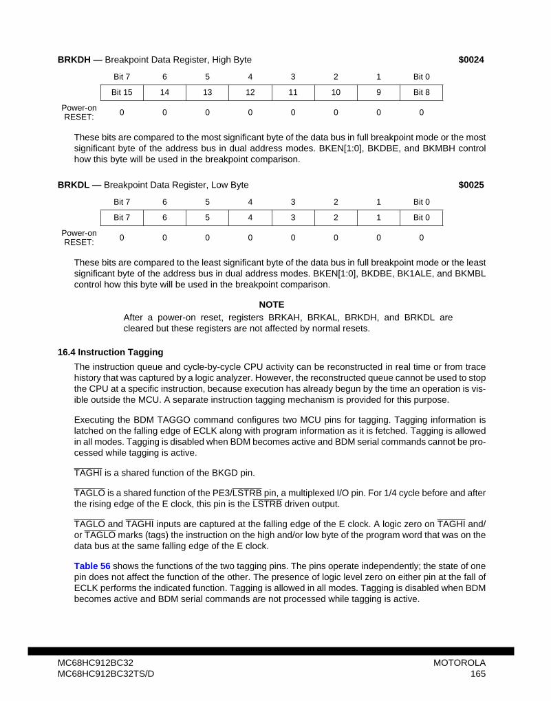
These bits are compared to the most significant byte of the data bus in full breakpoint mode or the mostsignificant byte of the address bus in dual address modes. BKEN[1:0], BKDBE, and BKMBH controlhow this byte will be used in the breakpoint comparison.
These bits are compared to the least significant byte of the data bus in full breakpoint mode or the leastsignificant byte of the address bus in dual address modes. BKEN[1:0], BKDBE, BK1ALE, and BKMBLcontrol how this byte will be used in the breakpoint comparison.
NOTEAfter a power-on reset, registers BRKAH, BRKAL, BRKDH, and BRKDL arecleared but these registers are not affected by normal resets.
16.4 Instruction Tagging
The instruction queue and cycle-by-cycle CPU activity can be reconstructed in real time or from tracehistory that was captured by a logic analyzer. However, the reconstructed queue cannot be used to stopthe CPU at a specific instruction, because execution has already begun by the time an operation is vis-ible outside the MCU. A separate instruction tagging mechanism is provided for this purpose.
Executing the BDM TAGGO command configures two MCU pins for tagging. Tagging information islatched on the falling edge of ECLK along with program information as it is fetched. Tagging is allowedin all modes. Tagging is disabled when BDM becomes active and BDM serial commands cannot be pro-cessed while tagging is active.
TAGHI is a shared function of the BKGD pin.
TAGLO is a shared function of the PE3/LSTRB pin, a multiplexed I/O pin. For 1/4 cycle before and afterthe rising edge of the E clock, this pin is the LSTRB driven output.
TAGLO and TAGHI inputs are captured at the falling edge of the E clock. A logic zero on TAGHI and/or TAGLO marks (tags) the instruction on the high and/or low byte of the program word that was on thedata bus at the same falling edge of the E clock.
Table 56 shows the functions of the two tagging pins. The pins operate independently; the state of onepin does not affect the function of the other. The presence of logic level zero on either pin at the fall ofECLK performs the indicated function. Tagging is allowed in all modes. Tagging is disabled when BDMbecomes active and BDM serial commands are not processed while tagging is active.
BRKDH — Breakpoint Data Register, High Byte $0024
Bit 7 6 5 4 3 2 1 Bit 0
Bit 15 14 13 12 11 10 9 Bit 8
Power-on RESET: 0 0 0 0 0 0 0 0
BRKDL — Breakpoint Data Register, Low Byte $0025
Bit 7 6 5 4 3 2 1 Bit 0
Bit 7 6 5 4 3 2 1 Bit 0
Power-on RESET: 0 0 0 0 0 0 0 0
MC68HC912BC32 MOTOROLAMC68HC912BC32TS/D 165
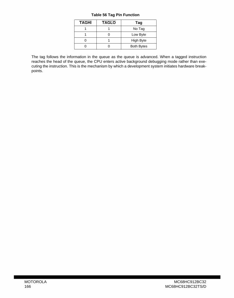
The tag follows the information in the queue as the queue is advanced. When a tagged instructionreaches the head of the queue, the CPU enters active background debugging mode rather than exe-cuting the instruction. This is the mechanism by which a development system initiates hardware break-points.
Table 56 Tag Pin Function
TAGHI TAGLO Tag
1 1 No Tag
1 0 Low Byte
0 1 High Byte
0 0 Both Bytes
MOTOROLA MC68HC912BC32166 MC68HC912BC32TS/D
17 Summary of ChangesThe following summary lists significant changes since previous versions. Typographical errors andother minor errors which do not affect technical content or organization have not been noted.
Section 1 IntroductionSec. 1.1. 2.7V-5.5V operation at 8 MHz changed to 4.5V-5.5V operation ay 8 MHz.
Flash EEPROM changed from 1 to 2-Kbyte Erase-Protected Boot Block.Analog-to-digital converter changed from 8-bit to 10-bit.
Table 1 MC68HC912BC32VFU8 data removed.MC68HC912BC32MFU8 data removed.MC68C912BC32FU8 data removed.MC68HC912BC32CFU8 data removed.MC68B912BC32FU8 data removed.
Section 3 SignalsSec. 3.3.2 Correction and addlitional information about E clock operation in single-chip, peripheral and
Stop modes.
Section 4 Register BlockTable 8 Address $0043 PWPRES, Bit 7 changed to 0.
Address $0054 PWCTL, bit 2 changed from RDPP to RDP.Address $0056, PORTP changed to PORTPP.Address $0057, DDRP changed to PORTPD.Address $0062, Bit 5 changed to AWAI.Address $0064, Bit 7 changed to S10BM.Addresses $0071, $0073, $0075, $0077, $0079, $007B, $007D and $007F added. Theseare registers ADR0-7 low.
Section 5 Operating Modes and Resource MappingSec. 5.1 Table 9, row 2 and row 6, DATA[15:0] changed to DATA[7:0]Sec. 5.3 Fourth paragraph, irrelevent information about memory expansion removed.Sec 5.3.4 MISC register, corrections and additional information regarding reset conditions.
Section 8 EEPROMSec. 8.2 EEPROT register, STPROT bit described
EEPROG register, note added to EELAT bit description
Section 11 Pulse-Width ModulatorPage 71 Added description of two additional initialization operations which occur in Center Aligne
mode.Page 72-74Updated versions of figures 15-17 included to replace block diagrams of PWM Left-Aligned
output channel, Center-Aligned output channel and PWM clock sourcesPage 75 Note added concerning bits 6 and 7.Page 76 Descriptions of bits PPOL3–PPOL0, the term “clock cycle” has been changed to “period.”
Note added concerning high and low time count in the duty registers.Page 77 In PWPRES, Bit 7 changed to 0.Page 78 PWSCAL0 register description, procedure for generating clock S0 has been corrected.
PWSCAL1 register description, procedure for generating clock S1 has been corrected.Page 79 PWCNTx register description, last sentence, removed phrase regarding center-aligned
mode.PWPERx register description, corrected formula for calculating period.PWPERx register reset condition changed to $FF
Page 80 PWDTYx register description, corrected formula for calculating duty cycle (CENTR=1).PWDTYx register reset condition changed to $FF.PWCTL bit 2 changed from RDPP to RDP.
MC68HC912B32 MOTOROLAMC68HC812A4TS/D 167
Page 81 PWTST register decription expanded to include functions only accessible in Special mode.
DISCP bit description, removed comment regarding center-aligned output mode.Note added to PORTPPconcerning write to this register.
Page 82 DDRD changed to PORTPD - Port P data direction register.Table 23, first row, Output is Low; second row, Output is High.
Throughout References to P clock changed to E clock
Section 13 Serial InterfacePage 97 Table 29, third row, fourth column (WOMS), 1 changed to 0.
Section 14 MSCAN12 ControllerPage 114 Figure 27. Bits in CIDMR0-3 registers changed from AC to AM.Page 115 Figure 28. Bits in CIDMR0-3 registers changed from AC to AM.Page 116 Figure 29. Bits in CIDMR0-3 registers changed from AC to AM.Page 118 Warning modified .Page 119 CIDAR0-3 and CIDARM0-3 changed to CIDAR0-7 and CIDAM0-7.Sec. 14.7.3.Additional information about access to registers added.Sec. 14.8. Footnote changed from timer channel....is integration dependent, to timer channel......is
PT0.Sec.14.12.6.Note added at end of section describing register state when SFTRES bit in CMCR0 is set.Sec. 14.12.7.Note added at end of section describing register state when SFTRES bit in CMCR0 is set.Sec. 14.12.8.Note added at end of section describing register state when SFTRES bit in CMCR0 is set.Sec. 14.12.9.Note added at end of section describing register state when SFTRES bit in CMCR0 is set.
Section 15 Analog-to-Digital ConverterPage 143 “The ATD is an 8-channel, 8-bit .....accurate to ± 1 LSB”, has been changed to; “The ATD
is an 8-channel, 10-bit........accurate to ± 2 least significant bits (LSB)”.Page 144 Bit 5 in ATDCTL2 changed from ASWAI to AWAI.Page 145 ATDCTL4 register, information added for calculating conversion time. Table 44 corrected.Page 146“ Writes to the ATD control registers initiates a new conversion sequence” is changed to “A
write to ATDCTL5 initiates a new conversion sequence.”
Section 16 Development SupportSec. 16.2.1 and Sec. 16.2.2 order swapped.Sec. 16.2.1Second paragraph, “256” (E-clock cycles) changed to “512”
Fourth paragraph, “Nine” (target E cycles) changed to “Ten”Fig. 43, “9” (cycles) changed to “10” and appropriate correction made to diagram
Sec. 16.2.3 Several paragraphs added with additional information about BDM commands.Table 48, Note 2, “ENTER_TAG_MODE” removed from footnote.
Sec. 16.2.4 Reset information added to INSTRUCTION register.Reset information corrected for STATUS register.Additional information added to STATUS register bit descriptions.
Sec. 16.3.1 Corrections and clarifications as to the effect of bits to breakpoint modes.Sec. 16.3.2 Additonal information added to BKPM bit description.
Additional information added regarding reset condition of registers BRKAH, BRKAL,BRKDH, and BRKDL
Sec. 16.4 Tag Pin Function table added with discussion
MOTOROLA MC68HC912B32168 MC68HC812A4TS/D

NOTES
MC68HC912B32 MOTOROLAMC68HC812A4TS/D 169

NOTES
MOTOROLA MC68HC912B32170 MC68HC812A4TS/D

MC68HC912B32 MOTOROLAMC68HC812A4TS/D 171
How to reach us:USA/EUROPE: Motorola Literature Distribution; P.O. Box 5405, Denver, Colorado 80217. 1-303-675-2140Mfax: [email protected] – TOUCHTONE 1- 602-244-6609. http://sps.motorola.com/mfax US & CANADA ONLY: http://sps.motorola.com/mfax
HOME PAGE: http://motorola.com/sps/JAPAN: Nippon Motorola Ltd.; Tatsumi-SPD-JLDC, 6F Seibu-Butsuryu-Center, 3-14-2 Tatsumi Koto-Ku,
Tokyo 135, Japan. 81-3-3521-8315HONG KONG: Motorola Semiconductors H.K. Ltd.; 8B Tai Ping Industrial Park, 51 Ting Kok Road, Tai Po, N.T.,
Hong Kong. 852-26629298CUSTOMER FOCUS CENTER: 1-800-521-6274
Mfax is a trademark of Motorola, Inc.© Motorola, Inc., 1997
Motorola reserves the right to make changes without further notice to any products herein. Motorola makes no warranty, representation or guarantee regarding thesuitability of its products for any particular purpose, nor does Motorola assume any liability arising out of the application or use of any product or circuit, and specificallydisclaims any and all liability, including without limitation consequential or incidental damages. "Typical" parameters can and do vary in different applications. All operatingparameters, including "Typicals" must be validated for each customer application by customer's technical experts. Motorola does not convey any license under its patentrights nor the rights of others. Motorola products are not designed, intended, or authorized for use as components in systems intended for surgical implant into the body, orother applications intended to support or sustain life, or for any other application in which the failure of the Motorola product could create a situation where personal injury ordeath may occur. Should Buyer purchase or use Motorola products for any such unintended or unauthorized application, Buyer shall indemnify and hold Motorola and itsofficers, employees, subsidiaries, affiliates, and distributors harmless against all claims, costs, damages, and expenses, and reasonable attorney fees arising out of, directlyor indirectly, any claim of personal injury or death associated with such unintended or unauthorized use, even if such claim alleges that Motorola was negligent regarding thedesign or manufacture of the part. Motorola and are registered trademarks of Motorola, Inc. Motorola, Inc. is an Equal Opportunity/Affirmative Action Employer.