Embed Size (px)
Citation preview
The Art of Electronics
Third Edition
At long last, here is the thoroughly revised and updated, and long-anticipated, third edition of the hugely successfulThe Art of Electronics. Widely accepted as the best single authoritative text and reference on electronic circuit design,both analog and digital, the first two editions were translated into eight languages, and sold more than a million copiesworldwide. The art of electronics is explained by stressing the methods actually used by circuit designers – a combinationof some basic laws, rules of thumb, and a nonmathematical treatment that encourages understanding why and how acircuit works.
Paul Horowitz is a Research Professor of Physics and of Electrical Engineering at Harvard University, where in 1974he originated the Laboratory Electronics course from which emerged The Art of Electronics. In addition to his work incircuit design and electronic instrumentation, his research interests have included observational astrophysics, x-ray andparticle microscopy, and optical interferometry. He is one of the pioneers of the search for intelligent life beyond Earth(SETI). He is the author of some 200 scientific articles and reports, has consulted widely for industry and government,and is the designer of numerous scientific and photographic instruments.
Winfield Hill is by inclination an electronics circuit-design guru. After dropping out of the Chemical Physics graduateprogram at Harvard University, and obtaining an E.E. degree, he began his engineering career at Harvard’s ElectronicsDesign Center. After 7 years of learning electronics at Harvard he founded Sea Data Corporation, where he spent 16 yearsdesigning instruments for Physical Oceanography. In 1988 he was recruited by Edwin Land to join the Rowland Institutefor Science. The institute subsequently merged with Harvard University in 2003. As director of the institute’s ElectronicsEngineering Lab he has designed some 500 scientific instruments. Recent interests include high-voltage RF (to 15 kV),high-current pulsed electronics (to 1200 A), low-noise amplifiers (to sub-nV and pA), and MOSFET pulse generators.


THE ART OF ELECTRONICSThird Edition
Paul Horowitz HARVARD UNIVERSITY
Winfield Hill ROWLAND INSTITUTE AT HARVARD

32 Avenue of the Americas, New York, NY 10013-2473, USA
Cambridge University Press is part of the University of Cambridge.
It furthers the University’s mission by disseminating knowledge in the pursuit ofeducation, learning, and research at the highest international levels of excellence.
www.cambridge.orgInformation on this title: www.cambridge.org/9780521809269
© Cambridge University Press, 1980, 1989, 2015
This publication is in copyright. Subject to statutory exceptionand to the provisions of relevant collective licensing agreements,no reproduction of any part may take place without the writtenpermission of Cambridge University Press.
First published 1980Second edition 1989Third edition 2015
Printed in the United States of America
A catalog record for this publication is available from the British Library.
ISBN 978-0-521-80926-9 Hardback
Cambridge University Press has no responsibility for the persistence oraccuracy of URLs for external or third-party Internet websites referred toin this publication and does not guarantee that any content on suchwebsites is, or will remain, accurate or appropriate.

To Vida and Ava


In Memoriam: Jim Williams, 1948–2011

CONTENTS
List of Tables xxii
Preface to the First Edition xxv
Preface to the Second Edition xxvii
Preface to the Third Edition xxix
ONE: Foundations 11.1 Introduction 11.2 Voltage, current, and resistance 1
1.2.1 Voltage and current 11.2.2 Relationship between voltage
and current: resistors 31.2.3 Voltage dividers 71.2.4 Voltage sources and current
sources 81.2.5 Thevenin equivalent circuit 91.2.6 Small-signal resistance 121.2.7 An example: “It’s too hot!” 13
1.3 Signals 131.3.1 Sinusoidal signals 141.3.2 Signal amplitudes and decibels 141.3.3 Other signals 151.3.4 Logic levels 171.3.5 Signal sources 17
1.4 Capacitors and ac circuits 181.4.1 Capacitors 181.4.2 RC circuits: V and I versus time 211.4.3 Differentiators 251.4.4 Integrators 261.4.5 Not quite perfect. . . 28
1.5 Inductors and transformers 281.5.1 Inductors 281.5.2 Transformers 30
1.6 Diodes and diode circuits 311.6.1 Diodes 311.6.2 Rectification 311.6.3 Power-supply filtering 321.6.4 Rectifier configurations for
power supplies 33
1.6.5 Regulators 341.6.6 Circuit applications of diodes 351.6.7 Inductive loads and diode
protection 381.6.8 Interlude: inductors as friends 39
1.7 Impedance and reactance 401.7.1 Frequency analysis of reactive
circuits 411.7.2 Reactance of inductors 441.7.3 Voltages and currents as
complex numbers 441.7.4 Reactance of capacitors and
inductors 451.7.5 Ohm’s law generalized 461.7.6 Power in reactive circuits 471.7.7 Voltage dividers generalized 481.7.8 RC highpass filters 481.7.9 RC lowpass filters 501.7.10 RC differentiators and
integrators in the frequencydomain 51
1.7.11 Inductors versus capacitors 511.7.12 Phasor diagrams 511.7.13 “Poles” and decibels per octave 521.7.14 Resonant circuits 521.7.15 LC filters 541.7.16 Other capacitor applications 541.7.17 Thevenin’s theorem generalized 55
1.8 Putting it all together – an AM radio 551.9 Other passive components 56
1.9.1 Electromechanical devices:switches 56
1.9.2 Electromechanical devices:relays 59
1.9.3 Connectors 591.9.4 Indicators 611.9.5 Variable components 63
1.10 A parting shot: confusing markings anditty-bitty components 641.10.1 Surface-mount technology: the
joy and the pain 65
ix
x Contents Art of Electronics Third Edition
Additional Exercises for Chapter 1 66Review of Chapter 1 68
TWO: Bipolar Transistors 712.1 Introduction 71
2.1.1 First transistor model: currentamplifier 72
2.2 Some basic transistor circuits 732.2.1 Transistor switch 732.2.2 Switching circuit examples 752.2.3 Emitter follower 792.2.4 Emitter followers as voltage
regulators 822.2.5 Emitter follower biasing 832.2.6 Current source 852.2.7 Common-emitter amplifier 872.2.8 Unity-gain phase splitter 882.2.9 Transconductance 89
2.3 Ebers–Moll model applied to basic tran-sistor circuits 902.3.1 Improved transistor model:
transconductance amplifier 902.3.2 Consequences of the
Ebers–Moll model: rules ofthumb for transistor design 91
2.3.3 The emitter follower revisited 932.3.4 The common-emitter amplifier
revisited 932.3.5 Biasing the common-emitter
amplifier 962.3.6 An aside: the perfect transistor 992.3.7 Current mirrors 1012.3.8 Differential amplifiers 102
2.4 Some amplifier building blocks 1052.4.1 Push–pull output stages 1062.4.2 Darlington connection 1092.4.3 Bootstrapping 1112.4.4 Current sharing in paralleled
BJTs 1122.4.5 Capacitance and Miller effect 1132.4.6 Field-effect transistors 115
2.5 Negative feedback 1152.5.1 Introduction to feedback 1162.5.2 Gain equation 1162.5.3 Effects of feedback on amplifier
circuits 1172.5.4 Two important details 1202.5.5 Two examples of transistor
amplifiers with feedback 1212.6 Some typical transistor circuits 123
2.6.1 Regulated power supply 1232.6.2 Temperature controller 1232.6.3 Simple logic with transistors
and diodes 123Additional Exercises for Chapter 2 124Review of Chapter 2 126
THREE: Field-Effect Transistors 1313.1 Introduction 131
3.1.1 FET characteristics 1313.1.2 FET types 1343.1.3 Universal FET characteristics 1363.1.4 FET drain characteristics 1373.1.5 Manufacturing spread of FET
characteristics 1383.1.6 Basic FET circuits 140
3.2 FET linear circuits 1413.2.1 Some representative JFETs: a
brief tour 1413.2.2 JFET current sources 1423.2.3 FET amplifiers 1463.2.4 Differential amplifiers 1523.2.5 Oscillators 1553.2.6 Source followers 1563.2.7 FETs as variable resistors 1613.2.8 FET gate current 163
3.3 A closer look at JFETs 1653.3.1 Drain current versus gate
voltage 1653.3.2 Drain current versus
drain-source voltage: outputconductance 166
3.3.3 Transconductance versus draincurrent 168
3.3.4 Transconductance versus drainvoltage 170
3.3.5 JFET capacitance 1703.3.6 Why JFET (versus MOSFET)
amplifiers? 1703.4 FET switches 171
3.4.1 FET analog switches 1713.4.2 Limitations of FET switches 1743.4.3 Some FET analog switch
examples 1823.4.4 MOSFET logic switches 184
3.5 Power MOSFETs 1873.5.1 High impedance, thermal
stability 1873.5.2 Power MOSFET switching
parameters 192
Art of Electronics Third Edition Contents xi
3.5.3 Power switching from logiclevels 192
3.5.4 Power switching cautions 1963.5.5 MOSFETs versus BJTs as
high-current switches 2013.5.6 Some power MOSFET circuit
examples 2023.5.7 IGBTs and other power
semiconductors 2073.6 MOSFETs in linear applications 208
3.6.1 High-voltage piezo amplifier 2083.6.2 Some depletion-mode circuits 2093.6.3 Paralleling MOSFETs 2123.6.4 Thermal runaway 214
Review of Chapter 3 219
FOUR: Operational Amplifiers 2234.1 Introduction to op-amps – the “perfect
component” 2234.1.1 Feedback and op-amps 2234.1.2 Operational amplifiers 2244.1.3 The golden rules 225
4.2 Basic op-amp circuits 2254.2.1 Inverting amplifier 2254.2.2 Noninverting amplifier 2264.2.3 Follower 2274.2.4 Difference amplifier 2274.2.5 Current sources 2284.2.6 Integrators 2304.2.7 Basic cautions for op-amp
circuits 2314.3 An op-amp smorgasbord 232
4.3.1 Linear circuits 2324.3.2 Nonlinear circuits 2364.3.3 Op-amp application:
triangle-wave oscillator 2394.3.4 Op-amp application: pinch-off
voltage tester 2404.3.5 Programmable pulse-width
generator 2414.3.6 Active lowpass filter 241
4.4 A detailed look at op-amp behavior 2424.4.1 Departure from ideal op-amp
performance 2434.4.2 Effects of op-amp limitations on
circuit behavior 2494.4.3 Example: sensitive
millivoltmeter 2534.4.4 Bandwidth and the op-amp
current source 254
4.5 A detailed look at selected op-amp cir-cuits 2544.5.1 Active peak detector 2544.5.2 Sample-and-hold 2564.5.3 Active clamp 2574.5.4 Absolute-value circuit 2574.5.5 A closer look at the integrator 2574.5.6 A circuit cure for FET leakage 2594.5.7 Differentiators 260
4.6 Op-amp operation with a single powersupply 2614.6.1 Biasing single-supply ac
amplifiers 2614.6.2 Capacitive loads 2644.6.3 “Single-supply” op-amps 2654.6.4 Example: voltage-controlled
oscillator 2674.6.5 VCO implementation:
through-hole versussurface-mount 268
4.6.6 Zero-crossing detector 2694.6.7 An op-amp table 270
4.7 Other amplifiers and op-amp types 2704.8 Some typical op-amp circuits 274
4.8.1 General-purpose lab amplifier 2744.8.2 Stuck-node tracer 2764.8.3 Load-current-sensing circuit 2774.8.4 Integrating suntan monitor 278
4.9 Feedback amplifier frequency compensa-tion 2804.9.1 Gain and phase shift versus
frequency 2814.9.2 Amplifier compensation
methods 2824.9.3 Frequency response of the
feedback network 284Additional Exercises for Chapter 4 287Review of Chapter 4 288
FIVE: Precision Circuits 2925.1 Precision op-amp design techniques 292
5.1.1 Precision versus dynamic range 2925.1.2 Error budget 293
5.2 An example: the millivoltmeter, revisited 2935.2.1 The challenge: 10 mV, 1%,
10 MΩ, 1.8 V single supply 2935.2.2 The solution: precision RRIO
current source 2945.3 The lessons: error budget, unspecified pa-
rameters 295
xii Contents Art of Electronics Third Edition
5.4 Another example: precision amplifier withnull offset 2975.4.1 Circuit description 297
5.5 A precision-design error budget 2985.5.1 Error budget 299
5.6 Component errors 2995.6.1 Gain-setting resistors 3005.6.2 The holding capacitor 3005.6.3 Nulling switch 300
5.7 Amplifier input errors 3015.7.1 Input impedance 3025.7.2 Input bias current 3025.7.3 Voltage offset 3045.7.4 Common-mode rejection 3055.7.5 Power-supply rejection 3065.7.6 Nulling amplifier: input errors 306
5.8 Amplifier output errors 3075.8.1 Slew rate: general
considerations 3075.8.2 Bandwidth and settling time 3085.8.3 Crossover distortion and output
impedance 3095.8.4 Unity-gain power buffers 3115.8.5 Gain error 3125.8.6 Gain nonlinearity 3125.8.7 Phase error and “active
compensation” 3145.9 RRIO op-amps: the good, the bad, and the
ugly 3155.9.1 Input issues 3165.9.2 Output issues 316
5.10 Choosing a precision op-amp 3195.10.1 “Seven precision op-amps” 3195.10.2 Number per package 3225.10.3 Supply voltage, signal range 3225.10.4 Single-supply operation 3225.10.5 Offset voltage 3235.10.6 Voltage noise 3235.10.7 Bias current 3255.10.8 Current noise 3265.10.9 CMRR and PSRR 3285.10.10 GBW, f T, slew rate and “m,”
and settling time 3285.10.11 Distortion 3295.10.12 “Two out of three isn’t bad”:
creating a perfect op-amp 3325.11 Auto-zeroing (chopper-stabilized) ampli-
fiers 3335.11.1 Auto-zero op-amp properties 3345.11.2 When to use auto-zero op-amps 338
5.11.3 Selecting an auto-zero op-amp 3385.11.4 Auto-zero miscellany 340
5.12 Designs by the masters: Agilent’s accurateDMMs 3425.12.1 It’s impossible! 3425.12.2 Wrong – it is possible! 3425.12.3 Block diagram: a simple plan 3435.12.4 The 34401A 6.5-digit front end 3435.12.5 The 34420A 7.5-digit frontend 344
5.13 Difference, differential, and instrumenta-tion amplifiers: introduction 347
5.14 Difference amplifier 3485.14.1 Basic circuit operation 3485.14.2 Some applications 3495.14.3 Performance parameters 3525.14.4 Circuit variations 355
5.15 Instrumentation amplifier 3565.15.1 A first (but naive) guess 3575.15.2 Classic three-op-amp
instrumentation amplifier 3575.15.3 Input-stage considerations 3585.15.4 A “roll-your-own”
instrumentation amplifier 3595.15.5 A riff on robust input protection 362
5.16 Instrumentation amplifier miscellany 3625.16.1 Input current and noise 3625.16.2 Common-mode rejection 3645.16.3 Source impedance and CMRR 3655.16.4 EMI and input protection 3655.16.5 Offset and CMRR trimming 3665.16.6 Sensing at the load 3665.16.7 Input bias path 3665.16.8 Output voltage range 3665.16.9 Application example: current
source 3675.16.10 Other configurations 3685.16.11 Chopper and auto-zero
instrumentation amplifiers 3705.16.12 Programmable gain
instrumentation amplifiers 3705.16.13 Generating a differential output 372
5.17 Fully differential amplifiers 3735.17.1 Differential amplifiers: basic
concepts 3745.17.2 Differential amplifier
application example: widebandanalog link 380
5.17.3 Differential-input ADCs 3805.17.4 Impedance matching 382
Art of Electronics Third Edition Contents xiii
5.17.5 Differential amplifier selectioncriteria 383
Review of Chapter 5 388
SIX: Filters 3916.1 Introduction 3916.2 Passive filters 391
6.2.1 Frequency response with RCfilters 391
6.2.2 Ideal performance with LCfilters 393
6.2.3 Several simple examples 3936.2.4 Enter active filters: an overview 3966.2.5 Key filter performance criteria 3996.2.6 Filter types 4006.2.7 Filter implementation 405
6.3 Active-filter circuits 4066.3.1 VCVS circuits 4076.3.2 VCVS filter design using our
simplified table 4076.3.3 State-variable filters 4106.3.4 Twin-T notch filters 4146.3.5 Allpass filters 4156.3.6 Switched-capacitor filters 4156.3.7 Digital signal processing 4186.3.8 Filter miscellany 422
Additional Exercises for Chapter 6 422Review of Chapter 6 423
SEVEN: Oscillators and Timers 4257.1 Oscillators 425
7.1.1 Introduction to oscillators 4257.1.2 Relaxation oscillators 4257.1.3 The classic oscillator–timer
chip: the 555 4287.1.4 Other relaxation-oscillator ICs 4327.1.5 Sinewave oscillators 4357.1.6 Quartz-crystal oscillators 4437.1.7 Higher stability: TCXO,
OCXO, and beyond 4507.1.8 Frequency synthesis: DDS and
PLL 4517.1.9 Quadrature oscillators 4537.1.10 Oscillator “jitter” 457
7.2 Timers 4577.2.1 Step-triggered pulses 4587.2.2 Monostable multivibrators 4617.2.3 A monostable application:
limiting pulse width and dutycycle 465
7.2.4 Timing with digital counters 465Review of Chapter 7 470
EIGHT: Low-Noise Techniques 4738.1 ‘‘Noise” 473
8.1.1 Johnson (Nyquist) noise 4748.1.2 Shot noise 4758.1.3 1/f noise (flicker noise) 4768.1.4 Burst noise 4778.1.5 Band-limited noise 4778.1.6 Interference 478
8.2 Signal-to-noise ratio and noise figure 4788.2.1 Noise power density and
bandwidth 4798.2.2 Signal-to-noise ratio 4798.2.3 Noise figure 4798.2.4 Noise temperature 480
8.3 Bipolar transistor amplifier noise 4818.3.1 Voltage noise, en 4818.3.2 Current noise in 4838.3.3 BJT voltage noise, revisited 4848.3.4 A simple design example:
loudspeaker as microphone 4868.3.5 Shot noise in current sources
and emitter followers 4878.4 Finding en from noise-figure specifica-
tions 4898.4.1 Step 1: NF versus IC 4898.4.2 Step 2: NF versus Rs 4898.4.3 Step 3: getting to en 4908.4.4 Step 4: the spectrum of en 4918.4.5 The spectrum of in 4918.4.6 When operating current is not
your choice 4918.5 Low-noise design with bipolar transistors 492
8.5.1 Noise-figure example 4928.5.2 Charting amplifier noise with en
and in 4938.5.3 Noise resistance 4948.5.4 Charting comparative noise 4958.5.5 Low-noise design with BJTs:
two examples 4958.5.6 Minimizing noise: BJTs, FETs,
and transformers 4968.5.7 A design example: 40¢
“lightning detector” preamp 4978.5.8 Selecting a low-noise bipolar
transistor 5008.5.9 An extreme low-noise design
challenge 505
xiv Contents Art of Electronics Third Edition
8.6 Low-noise design with JFETS 5098.6.1 Voltage noise of JFETs 5098.6.2 Current noise of JFETs 5118.6.3 Design example: low-noise
wideband JFET “hybrid”amplifiers 512
8.6.4 Designs by the masters: SR560low-noise preamplifier 512
8.6.5 Selecting low-noise JFETS 5158.7 Charting the bipolar–FET shootout 517
8.7.1 What about MOSFETs? 5198.8 Noise in differential and feedback ampli-
fiers 5208.9 Noise in operational amplifier circuits 521
8.9.1 Guide to Table 8.3: choosinglow-noise op-amps 525
8.9.2 Power-supply rejection ratio 5338.9.3 Wrapup: choosing a low-noise
op-amp 5338.9.4 Low-noise instrumentation
amplifiers and video amplifiers 5338.9.5 Low-noise hybrid op-amps 534
8.10 Signal transformers 5358.10.1 A low-noise wideband amplifier
with transformer feedback 5368.11 Noise in transimpedance amplifiers 537
8.11.1 Summary of the stabilityproblem 537
8.11.2 Amplifier input noise 5388.11.3 The enC noise problem 5388.11.4 Noise in the transresistance
amplifier 5398.11.5 An example: wideband JFET
photodiode amplifier 5408.11.6 Noise versus gain in the
transimpedance amplifier 5408.11.7 Output bandwidth limiting in
the transimpedance amplifier 5428.11.8 Composite transimpedance
amplifiers 5438.11.9 Reducing input capacitance:
bootstrapping thetransimpedance amplifier 547
8.11.10 Isolating input capacitance:cascoding the transimpedanceamplifier 548
8.11.11 Transimpedance amplifiers withcapacitive feedback 552
8.11.12 Scanning tunneling microscopepreamplifier 553
8.11.13 Test fixture for compensationand calibration 554
8.11.14 A final remark 5558.12 Noise measurements and noise sources 555
8.12.1 Measurement without a noisesource 555
8.12.2 An example: transistor-noisetest circuit 556
8.12.3 Measurement with a noisesource 556
8.12.4 Noise and signal sources 5588.13 Bandwidth limiting and rms voltage mea-
surement 5618.13.1 Limiting the bandwidth 5618.13.2 Calculating the integrated noise 5638.13.3 Op-amp “low-frequency noise”
with asymmetric filter 5648.13.4 Finding the 1/f corner frequency 5668.13.5 Measuring the noise voltage 5678.13.6 Measuring the noise current 5698.13.7 Another way: roll-your-own
fA/√
Hz instrument 5718.13.8 Noise potpourri 574
8.14 Signal-to-noise improvement by band-width narrowing 5748.14.1 Lock-in detection 575
8.15 Power-supply noise 5788.15.1 Capacitance multiplier 578
8.16 Interference, shielding, and grounding 5798.16.1 Interfering signals 5798.16.2 Signal grounds 5828.16.3 Grounding between instruments 583
Additional Exercises for Chapter 8 588Review of Chapter 8 590
NINE: Voltage Regulation and Power Conver-sion 594
9.1 Tutorial: from zener to series-pass linearregulator 5959.1.1 Adding feedback 596
9.2 Basic linear regulator circuits with theclassic 723 5989.2.1 The 723 regulator 5989.2.2 In defense of the beleaguered
723 6009.3 Fully integrated linear regulators 600
9.3.1 Taxonomy of linear regulatorICs 601
9.3.2 Three-terminal fixed regulators 601
Art of Electronics Third Edition Contents xv
9.3.3 Three-terminal adjustableregulators 602
9.3.4 317-style regulator: applicationhints 604
9.3.5 317-style regulator: circuitexamples 608
9.3.6 Lower-dropout regulators 6109.3.7 True low-dropout regulators 6119.3.8 Current-reference 3-terminal
regulator 6119.3.9 Dropout voltages compared 6129.3.10 Dual-voltage regulator circuit
example 6139.3.11 Linear regulator choices 6139.3.12 Linear regulator idiosyncrasies 6139.3.13 Noise and ripple filtering 6199.3.14 Current sources 620
9.4 Heat and power design 6239.4.1 Power transistors and
heatsinking 6249.4.2 Safe operating area 627
9.5 From ac line to unregulated supply 6289.5.1 ac-line components 6299.5.2 Transformer 6329.5.3 dc components 6339.5.4 Unregulated split supply – on
the bench! 6349.5.5 Linear versus switcher: ripple
and noise 6359.6 Switching regulators and dc–dc convert-
ers 6369.6.1 Linear versus switching 6369.6.2 Switching converter topologies 6389.6.3 Inductorless switching
converters 6389.6.4 Converters with inductors: the
basic non-isolated topologies 6419.6.5 Step-down (buck) converter 6429.6.6 Step-up (boost) converter 6479.6.7 Inverting converter 6489.6.8 Comments on the non-isolated
converters 6499.6.9 Voltage mode and current mode 6519.6.10 Converters with transformers:
the basic designs 6539.6.11 The flyback converter 6559.6.12 Forward converters 6569.6.13 Bridge converters 659
9.7 Ac-line-powered (“offline”) switchingconverters 660
9.7.1 The ac-to-dc input stage 6609.7.2 The dc-to-dc converter 662
9.8 A real-world switcher example 6659.8.1 Switchers: top-level view 6659.8.2 Switchers: basic operation 6659.8.3 Switchers: looking more closely 6689.8.4 The “reference design” 6719.8.5 Wrapup: general comments on
line-powered switching powersupplies 672
9.8.6 When to use switchers 6729.9 Inverters and switching amplifiers 6739.10 Voltage references 674
9.10.1 Zener diode 6749.10.2 Bandgap (VBE) reference 6799.10.3 JFET pinch-off (VP) reference 6809.10.4 Floating-gate reference 6819.10.5 Three-terminal precision
references 6819.10.6 Voltage reference noise 6829.10.7 Voltage references: additional
Comments 6839.11 Commercial power-supply modules 6849.12 Energy storage: batteries and capacitors 686
9.12.1 Battery characteristics 6879.12.2 Choosing a battery 6889.12.3 Energy storage in capacitors 688
9.13 Additional topics in power regulation 6909.13.1 Overvoltage crowbars 6909.13.2 Extending input-voltage range 6939.13.3 Foldback current limiting 6939.13.4 Outboard pass transistor 6959.13.5 High-voltage regulators 695
Review of Chapter 9 699
TEN: Digital Logic 70310.1 Basic logic concepts 703
10.1.1 Digital versus analog 70310.1.2 Logic states 70410.1.3 Number codes 70510.1.4 Gates and truth tables 70810.1.5 Discrete circuits for gates 71110.1.6 Gate-logic example 71210.1.7 Assertion-level logic notation 713
10.2 Digital integrated circuits: CMOS andBipolar (TTL) 71410.2.1 Catalog of common gates 71510.2.2 IC gate circuits 71710.2.3 CMOS and bipolar (“TTL”)
characteristics 718
xvi Contents Art of Electronics Third Edition
10.2.4 Three-state and open-collectordevices 720
10.3 Combinational logic 72210.3.1 Logic identities 72210.3.2 Minimization and Karnaugh
maps 72310.3.3 Combinational functions
available as ICs 72410.4 Sequential logic 728
10.4.1 Devices with memory: flip-flops 72810.4.2 Clocked flip-flops 73010.4.3 Combining memory and gates:
sequential logic 73410.4.4 Synchronizer 73710.4.5 Monostable multivibrator 73910.4.6 Single-pulse generation with
flip-flops and counters 73910.5 Sequential functions available as inte-
grated circuits 74010.5.1 Latches and registers 74010.5.2 Counters 74110.5.3 Shift registers 74410.5.4 Programmable logic devices 74510.5.5 Miscellaneous sequential
functions 74610.6 Some typical digital circuits 748
10.6.1 Modulo-n counter: a timingexample 748
10.6.2 Multiplexed LED digital display 75110.6.3 An n-pulse generator 752
10.7 Micropower digital design 75310.7.1 Keeping CMOS low power 754
10.8 Logic pathology 75510.8.1 dc problems 75510.8.2 Switching problems 75610.8.3 Congenital weaknesses of TTL
and CMOS 758Additional Exercises for Chapter 10 760Review of Chapter 10 762
ELEVEN: Programmable Logic Devices 76411.1 A brief history 76411.2 The hardware 765
11.2.1 The basic PAL 76511.2.2 The PLA 76811.2.3 The FPGA 76811.2.4 The configuration memory 76911.2.5 Other programmable logic
devices 76911.2.6 The software 769
11.3 An example: pseudorandom byte genera-tor 77011.3.1 How to make pseudorandom
bytes 77111.3.2 Implementation in standard
logic 77211.3.3 Implementation with
programmable logic 77211.3.4 Programmable logic – HDL
entry 77511.3.5 Implementation with a
microcontroller 77711.4 Advice 782
11.4.1 By Technologies 78211.4.2 By User Communities 785
Review of Chapter 11 787
TWELVE: Logic Interfacing 79012.1 CMOS and TTL logic interfacing 790
12.1.1 Logic family chronology – abrief history 790
12.1.2 Input and output characteristics 79412.1.3 Interfacing between logic
families 79812.1.4 Driving digital logic inputs 80212.1.5 Input protection 80412.1.6 Some comments about logic
inputs 80512.1.7 Driving digital logic from
comparators or op-amps 80612.2 An aside: probing digital signals 80812.3 Comparators 809
12.3.1 Outputs 81012.3.2 Inputs 81212.3.3 Other parameters 81512.3.4 Other cautions 816
12.4 Driving external digital loads from logiclevels 81712.4.1 Positive loads: direct drive 81712.4.2 Positive loads: transistor
assisted 82012.4.3 Negative or ac loads 82112.4.4 Protecting power switches 82312.4.5 nMOS LSI interfacing 826
12.5 Optoelectronics: emitters 82912.5.1 Indicators and LEDs 82912.5.2 Laser diodes 83412.5.3 Displays 836
12.6 Optoelectronics: detectors 840
Art of Electronics Third Edition Contents xvii
12.6.1 Photodiodes andphototransistors 841
12.6.2 Photomultipliers 84212.7 Optocouplers and relays 843
12.7.1 I: Phototransistor outputoptocouplers 844
12.7.2 II: Logic-output optocouplers 84412.7.3 III: Gate driver optocouplers 84612.7.4 IV: Analog-oriented
optocouplers 84712.7.5 V: Solid-state relays (transistor
output) 84812.7.6 VI: Solid-state relays (triac/SCR
output) 84912.7.7 VII: ac-input optocouplers 85112.7.8 Interrupters 851
12.8 Optoelectronics: fiber-optic digital links 85212.8.1 TOSLINK 85212.8.2 Versatile Link 85412.8.3 ST/SC glass-fiber modules 85512.8.4 Fully integrated high-speed
fiber-transceiver modules 85512.9 Digital signals and long wires 856
12.9.1 On-board interconnections 85612.9.2 Intercard connections 858
12.10 Driving Cables 85812.10.1 Coaxial cable 85812.10.2 The right way – I: Far-end
termination 86012.10.3 Differential-pair cable 86412.10.4 RS-232 87112.10.5 Wrapup 874
Review of Chapter 12 875
THIRTEEN : Digital meets Analog 87913.1 Some preliminaries 879
13.1.1 The basic performanceparameters 879
13.1.2 Codes 88013.1.3 Converter errors 88013.1.4 Stand-alone versus integrated 880
13.2 Digital-to-analog converters 88113.2.1 Resistor-string DACs 88113.2.2 R–2R ladder DACs 88213.2.3 Current-steering DACs 88313.2.4 Multiplying DACs 88413.2.5 Generating a voltage output 88513.2.6 Six DACs 88613.2.7 Delta–sigma DACs 888
13.2.8 PWM as digital-to-analogconverter 888
13.2.9 Frequency-to-voltage converters 89013.2.10 Rate multiplier 89013.2.11 Choosing a DAC 891
13.3 Some DAC application examples 89113.3.1 General-purpose laboratory
source 89113.3.2 Eight-channel source 89313.3.3 Nanoamp wide-compliance
bipolarity current source 89413.3.4 Precision coil driver 897
13.4 Converter linearity – a closer look 89913.5 Analog-to-digital converters 900
13.5.1 Digitizing: aliasing, samplingrate, and sampling depth 900
13.5.2 ADC Technologies 90213.6 ADCs I: Parallel (“flash”) encoder 903
13.6.1 Modified flash encoders 90313.6.2 Driving flash, folding, and RF
ADCs 90413.6.3 Undersampling flash-converter
example 90713.7 ADCs II: Successive approximation 908
13.7.1 A simple SAR example 90913.7.2 Variations on successive
approximation 90913.7.3 An A/D conversion example 910
13.8 ADCs III: integrating 91213.8.1 Voltage-to-frequency
conversion 91213.8.2 Single-slope integration 91413.8.3 Integrating converters 91413.8.4 Dual-slope integration 91413.8.5 Analog switches in conversion
applications (a detour) 91613.8.6 Designs by the masters:
Agilent’s world-class“multislope” converters 918
13.9 ADCs IV: delta–sigma 92213.9.1 A simple delta–sigma for our
suntan monitor 92213.9.2 Demystifying the delta–sigma
converter 92313.9.3 ΔΣ ADC and DAC 92313.9.4 The ΔΣ process 92413.9.5 An aside: “noise shaping” 92713.9.6 The bottom line 92813.9.7 A simulation 92813.9.8 What about DACs? 930
xviii Contents Art of Electronics Third Edition
13.9.9 Pros and Cons of ΔΣoversampling converters 931
13.9.10 Idle tones 93213.9.11 Some delta–sigma application
examples 93213.10 ADCs: choices and tradeoffs 938
13.10.1 Delta–sigma and thecompetition 938
13.10.2 Sampling versus averagingADCs: noise 940
13.10.3 Micropower A/D converters 94113.11 Some unusual A/D and D/A converters 942
13.11.1 ADE7753 multifunction acpower metering IC 943
13.11.2 AD7873 touchscreen digitizer 94413.11.3 AD7927 ADC with sequencer 94513.11.4 AD7730 precision
bridge-measurement subsystem 94513.12 Some A/D conversion system examples 946
13.12.1 Multiplexed 16-channeldata-acquisition system 946
13.12.2 Parallel multichannelsuccessive-approximationdata-acquisition system 950
13.12.3 Parallel multichanneldelta–sigma data-acquisitionsystem 952
13.13 Phase-locked loops 95513.13.1 Introduction to phase-locked
loops 95513.13.2 PLL components 95713.13.3 PLL design 96013.13.4 Design example: frequency
multiplier 96113.13.5 PLL capture and lock 96413.13.6 Some PLL applications 96613.13.7 Wrapup: noise and jitter
rejection in PLLs 97413.14 Pseudorandom bit sequences and noise
generation 97413.14.1 Digital-noise generation 97413.14.2 Feedback shift register
sequences 97513.14.3 Analog noise generation from
maximal-length sequences 97713.14.4 Power spectrum of shift-register
sequences 97713.14.5 Low-pass filtering 97913.14.6 Wrapup 98113.14.7 “True” random noise generators 982
13.14.8 A “hybrid digital filter” 983Additional Exercises for Chapter 13 984Review of Chapter 13 985
FOURTEEN: Computers, Controllers, andData Links 989
14.1 Computer architecture: CPU and data bus 99014.1.1 CPU 99014.1.2 Memory 99114.1.3 Mass memory 99114.1.4 Graphics, network, parallel, and
serial ports 99214.1.5 Real-time I/O 99214.1.6 Data bus 992
14.2 A computer instruction set 99314.2.1 Assembly language and
machine language 99314.2.2 Simplified “x86” instruction set 99314.2.3 A programming example 996
14.3 Bus signals and interfacing 99714.3.1 Fundamental bus signals: data,
address, strobe 99714.3.2 Programmed I/O: data out 99814.3.3 Programming the XY vector
display 100014.3.4 Programmed I/O: data in 100114.3.5 Programmed I/O: status
registers 100214.3.6 Programmed I/O: command
registers 100414.3.7 Interrupts 100514.3.8 Interrupt handling 100614.3.9 Interrupts in general 100814.3.10 Direct memory access 101014.3.11 Summary of PC104/ISA 8-bit
bus signals 101214.3.12 The PC104 as an embedded
single-board computer 101314.4 Memory types 1014
14.4.1 Volatile and non-volatilememory 1014
14.4.2 Static versus dynamic RAM 101514.4.3 Static RAM 101614.4.4 Dynamic RAM 101814.4.5 Nonvolatile memory 102114.4.6 Memory wrapup 1026
14.5 Other buses and data links: overview 102714.6 Parallel buses and data links 1028
14.6.1 Parallel chip “bus” interface –an example 1028
Art of Electronics Third Edition Contents xix
14.6.2 Parallel chip data links – twohigh-speed examples 1030
14.6.3 Other parallel computer buses 103014.6.4 Parallel peripheral buses and
data links 103114.7 Serial buses and data links 1032
14.7.1 SPI 103214.7.2 I2C 2-wire interface (“TWI”) 103414.7.3 Dallas–Maxim “1-wire” serial
interface 103514.7.4 JTAG 103614.7.5 Clock-be-gone: clock recovery 103714.7.6 SATA, eSATA, and SAS 103714.7.7 PCI Express 103714.7.8 Asynchronous serial (RS-232,
RS-485) 103814.7.9 Manchester coding 103914.7.10 Biphase coding 104114.7.11 RLL binary: bit stuffing 104114.7.12 RLL coding: 8b/10b and others 104114.7.13 USB 104214.7.14 FireWire 104214.7.15 Controller Area Network
(CAN) 104314.7.16 Ethernet 1045
14.8 Number formats 104614.8.1 Integers 104614.8.2 Floating-point numbers 1047
Review of Chapter 14 1049
FIFTEEN: Microcontrollers 105315.1 Introduction 105315.2 Design example 1: suntan monitor (V) 1054
15.2.1 Implementation with amicrocontroller 1054
15.2.2 Microcontroller code(“firmware”) 1056
15.3 Overview of popular microcontroller fam-ilies 105915.3.1 On-chip peripherals 1061
15.4 Design example 2: ac power control 106215.4.1 Microcontroller implementation 106215.4.2 Microcontroller code 1064
15.5 Design example 3: frequency synthesizer 106515.5.1 Microcontroller code 1067
15.6 Design example 4: thermal controller 106915.6.1 The hardware 107015.6.2 The control loop 107415.6.3 Microcontroller code 1075
15.7 Design example 5: stabilized mechanicalplatform 1077
15.8 Peripheral ICs for microcontrollers 107815.8.1 Peripherals with direct
connection 107915.8.2 Peripherals with SPI connection 108215.8.3 Peripherals with I2C connection 108415.8.4 Some important hardware
constraints 108615.9 Development environment 1086
15.9.1 Software 108615.9.2 Real-time programming
constraints 108815.9.3 Hardware 108915.9.4 The Arduino Project 1092
15.10 Wrapup 109215.10.1 How expensive are the tools? 109215.10.2 When to use microcontrollers 109315.10.3 How to select a microcontroller 109415.10.4 A parting shot 1094
Review of Chapter 15 1095
APPENDIX A: Math Review 1097A.1 Trigonometry, exponentials, and loga-
rithms 1097A.2 Complex numbers 1097A.3 Differentiation (Calculus) 1099
A.3.1 Derivatives of some commonfunctions 1099
A.3.2 Some rules for combiningderivatives 1100
A.3.3 Some examples ofdifferentiation 1100
APPENDIX B: How to Draw Schematic Dia-grams 1101
B.1 General principles 1101B.2 Rules 1101B.3 Hints 1103B.4 A humble example 1103
APPENDIX C: Resistor Types 1104C.1 Some history 1104C.2 Available resistance values 1104C.3 Resistance marking 1105C.4 Resistor types 1105C.5 Confusion derby 1105
APPENDIX D: Thevenin’s Theorem 1107D.1 The proof 1107
xx Contents Art of Electronics Third Edition
D.1.1 Two examples – voltagedividers 1107
D.2 Norton’s theorem 1108D.3 Another example 1108D.4 Millman’s theorem 1108
APPENDIX E: LC Butterworth Filters 1109E.1 Lowpass filter 1109E.2 Highpass filter 1109E.3 Filter examples 1109
APPENDIX F: Load Lines 1112F.1 An example 1112F.2 Three-terminal devices 1112F.3 Nonlinear devices 1113
APPENDIX G: The Curve Tracer 1115
APPENDIX H: Transmission Lines andImpedance Matching 1116
H.1 Some properties of transmission lines 1116H.1.1 Characteristic impedance 1116H.1.2 Termination: pulses 1117H.1.3 Termination: sinusoidal signals 1120H.1.4 Loss in transmission lines 1121
H.2 Impedance matching 1122H.2.1 Resistive (lossy) broadband
matching network 1123H.2.2 Resistive attenuator 1123H.2.3 Transformer (lossless)
broadband matching network 1124H.2.4 Reactive (lossless) narrowband
matching networks 1125H.3 Lumped-element delay lines and pulse-
forming networks 1126H.4 Epilogue: ladder derivation of characteris-
tic impedance 1127H.4.1 First method: terminated line 1127H.4.2 Second method: semi-infinite
line 1127H.4.3 Postscript: lumped-element
delay lines 1128
APPENDIX I: Television: A Compact Tutorial 1131I.1 Television: video plus audio 1131
I.1.1 The audio 1131I.1.2 The video 1132
I.2 Combining and sending the audio + video:modulation 1133
I.3 Recording analog-format broadcast or ca-ble television 1135
I.4 Digital television: what is it? 1136I.5 Digital television: broadcast and cable de-
livery 1138I.6 Direct satellite television 1139I.7 Digital video streaming over internet 1140I.8 Digital cable: premium services and con-
ditional access 1141I.8.1 Digital cable: video-on-demand 1141I.8.2 Digital cable: switched
broadcast 1142I.9 Recording digital television 1142I.10 Display technology 1142I.11 Video connections: analog and digital 1143
APPENDIX J: SPICE Primer 1146J.1 Setting up ICAP SPICE 1146J.2 Entering a Diagram 1146J.3 Running a simulation 1146
J.3.1 Schematic entry 1146J.3.2 Simulation: frequency sweep 1147J.3.3 Simulation: input and output
waveforms 1147J.4 Some final points 1148J.5 A detailed example: exploring amplifier
distortion 1148J.6 Expanding the parts database 1149
APPENDIX K: “Where Do I Go to Buy Elec-tronic Goodies?” 1150
APPENDIX L: Workbench Instruments andTools 1152
APPENDIX M: Catalogs, Magazines, Data-books 1153
APPENDIX N: Further Reading and Refer-ences 1154
APPENDIX O: The Oscilloscope 1158O.1 The analog oscilloscope 1158
O.1.1 Vertical 1158O.1.2 Horizontal 1158O.1.3 Triggering 1159O.1.4 Hints for beginners 1160O.1.5 Probes 1160O.1.6 Grounds 1161O.1.7 Other analog scope features 1161
O.2 The digital oscilloscope 1162

Art of Electronics Third Edition Contents xxi
O.2.1 What’s different? 1162O.2.2 Some cautions 1164
APPENDIX P: Acronyms and Abbreviations 1166
Index 1171
LIST OF TABLES
1.1. Representative Diodes. 322.1. Representative Bipolar Transistors. 742.2. Bipolar Power Transistors. 1063.1. JFET Mini-table. 1413.2. Selected Fast JFET-input Op-amps. 1553.3. Analog Switches. 1763.4a. MOSFETs – Small n-channel (to 250V), and
p-channel (to 100V). 1883.4b. n-channel Power MOSFETs, 55 V to 4500 V. 1893.5. MOSFET Switch Candidates. 2063.6. Depletion-mode n-channel MOSFETs. 2103.7. Junction Field-Effect Transistors (JFETs). 2173.8. Low-side MOSFET Gate Drivers. 2184.1. Op-amp Parameters. 2454.2a. Representative Operational Amplifiers. 2714.2b. Monolithic Power and High-voltage
Op-amps. 2725.1. Millivoltmeter Candidate Op-amps. 2965.2. Representative Precision Op-amps. 3025.3. Nine Low-input-current Op-amps. 3035.4. Representative High-speed Op-amps. 3105.5. “Seven” Precision Op-amps: High Voltage. 3205.6. Chopper and Auto-zero Op-amps. 3355.7. Selected Difference Amplifiers. 3535.8. Selected Instrumentation Amplifiers 3635.9. Selected Programmable-gain Instrumentation
Amplifiers. 3705.10. Selected Differential Amplifiers. 3756.1. Time-domain Performance Comparison for
Lowpass Filters. 4066.2. VCVS Lowpass Filters. 4087.1. 555-type Oscillators. 4307.2. Oscillator Types. 4527.3. Monostable Multivibrators. 4627.4. “Type 123” Monostable Timing. 4638.1a. Low-noise Bipolar Transistors (BJTs). 5018.1b. Dual Low-noise BJTs. 5028.2. Low-noise Junction FETs (JFETs). 5168.3a. Low-noise BJT-input Op-amps. 5228.3b. Low-noise FET-input Op-amps. 5238.3c. High-speed Low-noise Op-amps. 524
8.4. Noise Integrals. 5648.5. Auto-zero Noise Measurements. 5699.1. 7800-style Fixed Regulators. 6029.2. Three-terminal Adjustable Voltage Regulators
(LM317-style). 6059.3. Low-dropout Linear Voltage Regulators. 6149.4. Selected Charge-pump Converters. 6409.5a. Voltage-mode Integrated Switching
Regulators. 6539.5b. Selected Current-mode Integrated Switching
Regulators. 6549.6. External-switch Controllers. 6589.7. Shunt (2-terminal) Voltage References. 6779.8. Series (3-terminal) Voltage References. 6789.9. Battery Choices. 6899.10. Energy Storage: Capacitor Versus Battery. 69010.1. Selected Logic Families. 70610.2. 4-bit Signed Integers in Three Systems of
Representation. 70710.3. Standard Logic Gates. 71610.4. Logic Identities. 72210.5. Selected Counter ICs. 74210.6. Selected Reset/Supervisors. 75612.1. Representative Comparators. 81212.2. Comparators. 81312.3. Power Logic Registers. 81912.4. A Few Protected MOSFETs. 82512.5. Selected High-side Switches. 82612.6. Selected Panel-mount LEDs. 83213.1. Six Digital-to-analog Converters. 88913.2. Selected Digital-to-analog Converters. 89313.3. Multiplying DACs. 89413.4. Selected Fast ADCs. 90513.5. Successive-approximation ADCs. 91013.6. Selected Micropower ADCs. 91613.7. 4053-style SPDT Switches. 91713.8. Agilent’s Multislope III ADCs. 92113.9. Selected Delta–sigma ADCs. 93513.10. Audio Delta–sigma ADCs. 93713.11. Audio ADCs. 93913.12. Speciality ADCs. 942
xxii

Art of Electronics Third Edition List of Tables xxiii
13.13. Phase-locked Loop ICs. 97213.14. Single-tap LFSRs. 97613.15. LFSRs with Length a Multiple of 8. 97614.1. Simplified x86 Instruction Set. 99414.2. PC104/ISA Bus Signals. 1013
14.3. Common Buses and Data Links. 102914.4. RS-232 Signals. 103914.5. ASCII Codes. 1040C.1. Selected Resistor Types. 1106E.1. Butterworth Lowpass Filters. 1110H.1. Pi and T Attenuators. 1124
VOLTAGE REGULATION ANDPOWER CONVERSION
CHAPTER 9The control and conversion of power – power engineering– is a rich and exciting subfield of electrical engineeringand electronic design. It encompasses applications rang-ing from high-voltage (kilovolts and upward) and high-current (kiloamperes and upward) dc transmission, trans-portation, and pulsing, all the way down to low-power fixedand portable (battery-operated) and micropower (energy-harvesting) applications. Perhaps of most interest to us inthe context of circuit design; it includes the production ofthe voltages and currents needed in electronic circuit de-sign.
Nearly all electronic circuits, from simple transistor andop-amp circuits up to elaborate digital and microproces-sor systems, require one or more sources of stable dc volt-age. The simple transformer–bridge–capacitor unregulatedpower supplies we discussed in Chapter 1 are not gener-ally adequate because their output voltages change withload current and line voltage, and because they have sig-nificant amounts of powerline ripple (120 Hz or 100 Hz).Fortunately, it is easy to construct highly stable power sup-plies, by using negative feedback to compare the dc outputvoltage with a stable voltage reference. Such regulated sup-plies are in universal use and can be simply constructedwith integrated circuit voltage-regulator chips, requiringonly a source of unregulated dc input (from a transformer–rectifier–capacitor combination,1 a battery, or some othersource of dc input) and a few other components.
In this chapter we will see how to construct volt-age regulators by using special-purpose integrated cir-cuits. The same circuit techniques can be used to makeregulators with discrete components (transistors, resistors,etc.), but because of the availability of inexpensive high-performance regulator chips, there is usually no advantageto using discrete components in new designs. Voltage reg-ulators get us into the domain of high power dissipation,
1 Sometimes the transformer can be omitted; this is most commonly donein switchmode power supplies (SMPSs), see §9.6.
so we will be talking about heatsinking and techniques like“foldback limiting” to limit transistor operating tempera-tures and prevent circuit damage. These techniques can beused for all sorts of power circuits, including power ampli-fiers. With the knowledge of regulators we will have at thatpoint, we will be able to go back and discuss the design ofthe unregulated supply in some detail. In this chapter wewill also look at voltage references and voltage-referenceICs, devices with plenty of uses outside of power-supplydesign (for example in analog–digital conversion).
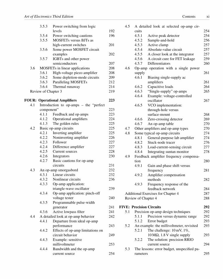
We begin with the linear regulator, in which feedbackcontrols conduction in a series voltage-dropping “passtransistor” to hold constant the output voltage. Later wetreat the important topic of switching regulators, in whichone or more transistors are switched rapidly to transfer en-ergy, via an inductor (or capacitor) to the load, again withvoltage-regulating feedback. In a nutshell, linear regulatorsare simpler and generate “cleaner” (i.e., noise-free) dc out-put; switchers (the nickname for switching regulators andconverters) are more compact and efficient (Figure 9.1), butnoisier and usually more complex.
It would be wrong to leave the impression that voltageregulators are used exclusively in ac-powered dc supplies.In addition to their use in creating stable dc voltages fromthe ac powerline, voltage regulators are used widely alsoto produce additional dc voltages from an existing regu-lated dc voltage within a circuit: it’s common to see, forexample, a regulator that accepts an existing +5 V inputand generates a +2.5 V or +3.3 V output; this is easily donewith a linear regulator, in which feedback controls the volt-age drop to maintain constant (and reduced) output voltage.Perhaps more surprising, you can use a switching regulatorto convert a given dc input to a larger output voltage, to anoutput voltage of opposite polarity, or to a constant current(for example, to drive a string of LEDs). These applica-tions are particularly relevant to battery-powered devices.The more general term power converter is often used insuch applications, which include also creating an ac outputfrom a dc input.
594
Art of Electronics Third Edition Voltage Regulation and Power Conversion 595
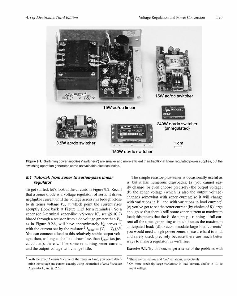
Figure 9.1. Switching power supplies (“switchers”) are smaller and more efficient than traditional linear regulated power supplies, but theswitching operation generates some unavoidable electrical noise.
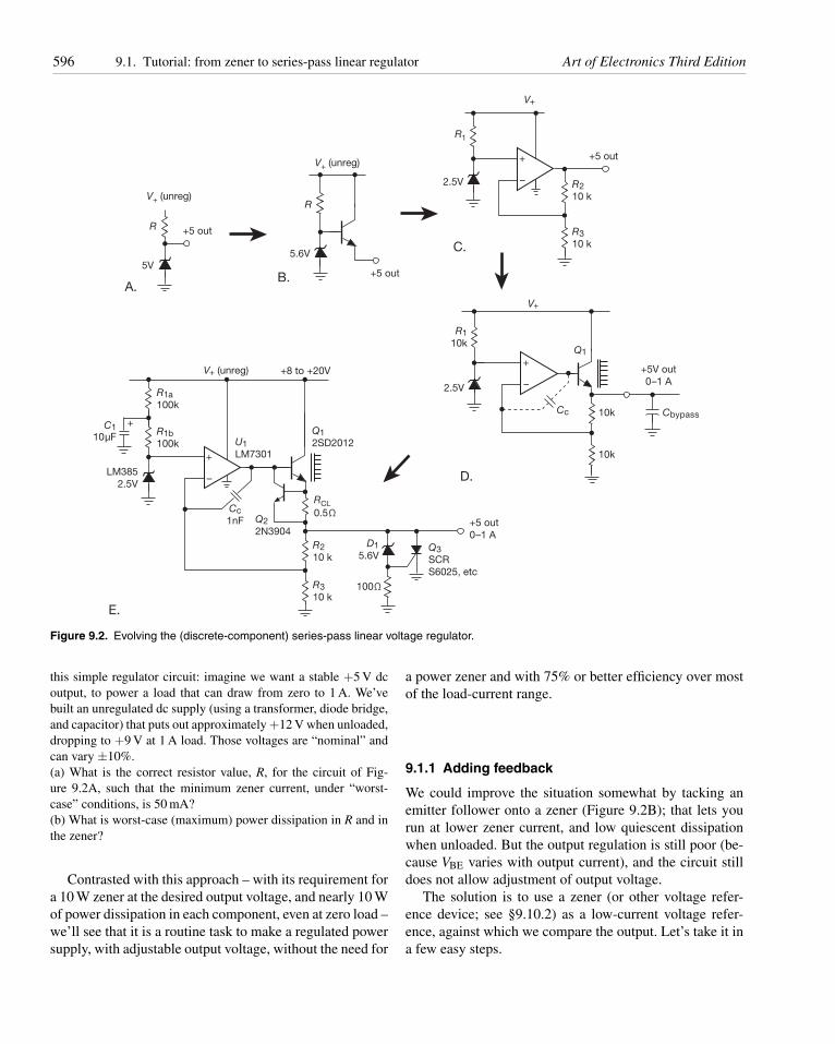
9.1 Tutorial: from zener to series-pass linearregulator
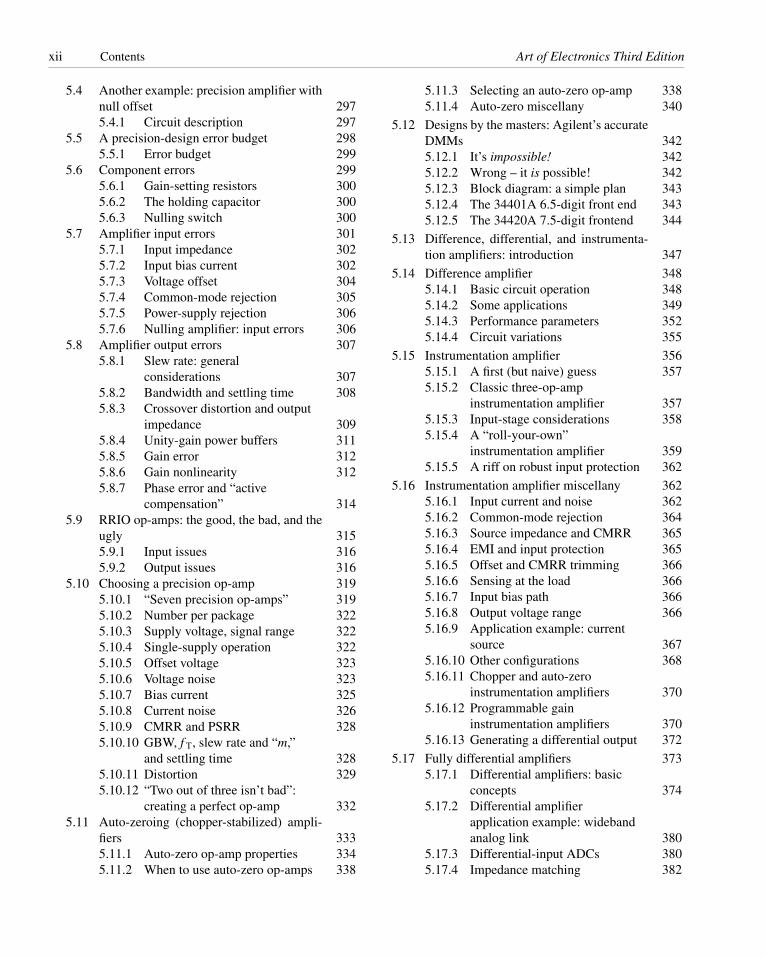
To get started, let’s look at the circuits in Figure 9.2. Recallthat a zener diode is a voltage regulator, of sorts: it drawsnegligible current until the voltage across it is brought closeto its zener voltage VZ, at which point the current risesabruptly (look back at Figure 1.15 for a reminder). So azener (or 2-terminal zener-like reference IC, see §9.10.2)biased through a resistor from a dc voltage greater than VZ,as in Figure 9.2A, will have approximately VZ across it,with the current set by the resistor:2 Izener = (V+ −VZ)/R.You can connect a load to this relatively stable output volt-age; then, as long as the load draws less than Izener (as justcalculated), there will be some remaining zener current,and the output voltage will change little.
2 With the exact I versus V curve of the zener in hand, you could deter-mine the voltage and current exactly, using the method of load lines; seeAppendix F, and §3.2.6B.
The simple resistor-plus-zener is occasionally useful asis, but it has numerous drawbacks: (a) you cannot eas-ily change (or even choose precisely) the output voltage;(b) the zener voltage (which is also the output voltage)changes somewhat with zener current; so it will changewith variations in V+ and with variations in load current;3
(c) you’ve got to set the zener current (by choice of R) largeenough so that there’s still some zener current at maximumload; this means that the V+ dc supply is running at full cur-rent all the time, generating as much heat as the maximumanticipated load; (d) to accommodate large load currents4
you would need a high-power zener; these are hard to find,and rarely used, precisely because there are much betterways to make a regulator, as we’ll see.
Exercise 9.1. Try this out, to get a sense of the problems with
3 These are called line and load variations, respectively.4 Or, more precisely, large variations in load current, and/or in V+ dc
input voltage.
596 9.1. Tutorial: from zener to series-pass linear regulator Art of Electronics Third Edition
V+ (unreg)
R2
10 k
R3
10 k
+5 out
A.B.
+
–
5V
R
V+ (unreg)
+5 out
+5 out
+5V out
0–1 A
5.6V
R
C.
V+
2.5V
LM385
2.5V
U1
LM7301
R1
+
–
D.
V+
2.5V
R1
10kQ1
Cc
Cc
1nF
Cbypass10k
10k+
+
–
E.
V+ (unreg)
R1a
100k
C1
10μFR1b
100k
Q2
2N3904
Q1
2SD2012
RCL
0.5Ω
R2
10 kQ3
SCR
S6025, etc
+5 out
0–1 AD1
5.6V
100ΩR3
10 k
+8 to +20V
Figure 9.2. Evolving the (discrete-component) series-pass linear voltage regulator.
this simple regulator circuit: imagine we want a stable +5 V dcoutput, to power a load that can draw from zero to 1 A. We’vebuilt an unregulated dc supply (using a transformer, diode bridge,and capacitor) that puts out approximately +12 V when unloaded,dropping to +9 V at 1 A load. Those voltages are “nominal” andcan vary ±10%.(a) What is the correct resistor value, R, for the circuit of Fig-ure 9.2A, such that the minimum zener current, under “worst-case” conditions, is 50 mA?(b) What is worst-case (maximum) power dissipation in R and inthe zener?
Contrasted with this approach – with its requirement fora 10 W zener at the desired output voltage, and nearly 10 Wof power dissipation in each component, even at zero load –we’ll see that it is a routine task to make a regulated powersupply, with adjustable output voltage, without the need for
a power zener and with 75% or better efficiency over mostof the load-current range.
9.1.1 Adding feedback
We could improve the situation somewhat by tacking anemitter follower onto a zener (Figure 9.2B); that lets yourun at lower zener current, and low quiescent dissipationwhen unloaded. But the output regulation is still poor (be-cause VBE varies with output current), and the circuit stilldoes not allow adjustment of output voltage.
The solution is to use a zener (or other voltage refer-ence device; see §9.10.2) as a low-current voltage refer-ence, against which we compare the output. Let’s take it ina few easy steps.
Art of Electronics Third Edition 9.1.1. Adding feedback 597
A. Zener plus “amplifier”First we solve the problem of adjustability by following thezener reference with a simple dc amplifier (Figure 9.2C).Now the zener current can be small, just enough to ensurea stable reference. For typical zeners this might be a fewmilliamps, whereas for an IC voltage reference, 0.1–1 mAwill usually suffice. This circuit lets you adjust the outputvoltage: Vout = VZ(1 + R2/R3). But note that you are lim-ited to having Vout ≥ VZ; note also that the output voltagecomes from an op-amp, so it can at most reach V+, with anoutput current limited by the op-amp’s Iout(max), typically20 mA. We will overcome both these limits.
B. Adding outboard pass transistorMore output current is easy – just add an npn follower, toboost the output current by a factor of β . You might betempted to just hang the follower on the op-amp’s output,but that would be a mistake: the output voltage would bedown by a VBE drop, roughly 0.6 V. You could, of course,adjust the ratio R2/R3 to compensate. But the VBE dropis imprecise, varying both with temperature and with loadcurrent, and so the output voltage would vary accordingly.The better way is to close the feedback loop around thepass transistor, as in Figure 9.2D; that way the error am-plifier sees the actual output voltage, holding it stable viathe circuit’s loop gain. The inclusion of the output emit-ter follower boosts the op-amp’s Iout(max) by the beta ofQ1, giving us an available output current of an ampere orso. (We could use a Darlington, instead, for more current;another possibility is an n-channel MOSFET.) Q1 will bedissipating 5–10 W at maximum output current, so you’llneed a heatsink (more on this in §9.4.1). And, as we’ll seenext, you’ll also need to add a compensation capacitor CC
to ensure stability.
C. Some important additionsOur voltage regulator circuit is nearly complete, but lacksa couple of essential features, related to loop stability andovercurrent protection.
Feedback loop stabilityRegulated power supplies are used to power electronic cir-cuits, typically festooned with many bypass capacitors be-tween the dc rails and ground. (Those bypass capacitors, ofcourse, are needed to maintain a pleasantly low impedanceat all signal frequencies.) Thus the dc supply sees a largecapacitive load, which, when combined with the finite out-put resistance of the pass transistor (and overcurrent senseresistor, if present), causes a lagging phase shift and pos-sible oscillation. We’ve shown the load capacitance in Fig-
ure 9.2D as Cbypass, a portion of which might be includedexplicitly (as a real capacitor) in the power supply itself.
The solution here, as with the op-amp circuits we wor-ried about earlier (§4.9), is to include some form of fre-quency compensation. That is most simply done (as itis within op-amps) with a Miller feedback capacitor CC
around the inverting gain stage, as shown. Typical val-ues are 100–1000 pF, usually found experimentally (“cut-and-try”) by increasing CC until the output shows a well-damped response to a step change in load (and then dou-bling that, to provide a good margin of stability). The ICregulators we’ll see later will either include internal com-pensation, or they’ll give you suggested values for com-pensation components.
Overcurrent protectionThe circuit as drawn in Figure 9.2D does not deal well witha short-circuit load condition.5 With the output shorted toground, feedback will act to force the op-amp’s maximumoutput current into the pass transistor’s base; so that IB of20–40 mA will be multiplied by Q1’s beta (which mightrange from 50 to 250, say), to produce an output current of1 A to 10 A. Assuming the unregulated V+ input can supplyit, such a current will cause excessive heating in the passtransistor, as well as interesting forms of damage to themisbehaving load.
The solution is to include some form of overcurrentprotection, most simply the classic current-limiting circuitconsisting of Q2 and RCL in Figure 9.2E. Here RCL isa low-value sense resistor, chosen to drop approximately0.6 V (a VBE diode drop) at a current somewhat larger thanthe maximum rated current; for example, we might chooseRCL = 5Ω in a 100 mA supply. The drop across RCL is ap-plied across Q2’s base–emitter, turning it on at the desiredmaximum output current; Q2’s conduction robs base cur-rent from Q1, preventing further increase of output current.Note that the current-limit sense transistor Q2 does not han-dle high voltage, high current, or high power; it sees at mosttwo diode drops from collector to emitter, the op-amp’smaximum output current, and the product of those two, re-spectively. During an overcurrent load condition, then, ittypically would have to handle VCE ≤ 1.5 V at IC ≤ 40 mA,or 60 mW; that’s peanuts for any general-purpose small-signal transistor.
Later we’ll see variations on this simple overcurrentprotection theme, including methods that limit to an
5 Engineers like to refer to various bad situations such as this under thegeneral rubric of fault conditions.
598 9.2. Basic linear regulator circuits with the classic 723 Art of Electronics Third Edition
adjustable and stable current limit, and the techniqueknown as foldback current limiting (§9.13.3).
Zener bias; overvoltage crowbarWe’ve shown two additional wrinkles in Figure 9.2E. First,we split the zener biasing resistor R1 and bypassed the mid-point, to filter out ripple current. By choosing the time con-stant (τ = (R1a‖R1b)C1) to be long compared with the rip-ple period of 8.3 ms, the zener sees ripple-free bias current.(You wouldn’t bother with this if the dc supply V+ werealready free of ripple, for example a regulated dc supplyof higher voltage.) Alternatively, you could use a currentsource to bias the zener.
Second, we’ve shown an “overvoltage crowbar” protec-tion circuit consisting of D1, Q3, and the 100 Ω resistor. Itsfunction is to short the output if some circuit fault causesthe output voltage to exceed about 6.2 V (this can happeneasily enough, for example if the pass transistor Q1 failsby having a collector-to-emitter short, or if a humble com-ponent like resistor R2 becomes open-circuited.). Q3 is anSCR (silicon-controlled rectifier), a device that is normallynonconducting but that goes into saturation when the gate–cathode junction is forward-biased. Once turned on, it willnot turn off again until anode current is removed exter-nally. In this case, gate current flows when the output ex-ceeds D1’s zener voltage plus a diode drop. When that hap-pens, the regulator will go into a current-limiting condition,with the output held near ground by the SCR. If the failurethat produces the abnormally high output also disables thecurrent-limiting circuit (e.g., a collector-to-emitter short inQ1), then the crowbar will sink a very large current. Forthis reason it is a good idea to include a fuse somewherein the power supply, as shown for example in Figure 9.48.We will treat overvoltage crowbar circuits in more detail in§§9.13.1 and 9x.7.
Exercise 9.2. Explain how an open circuit at R2 causes the outputto soar. What voltage, approximately, would then appear at theoutput?
9.2 Basic linear regulator circuits with theclassic 723
In the preceding tutorial we evolved the basic form of thelinear series pass regulator: voltage reference, pass tran-sistor, error amplifier, and provisions for loop stability andovervoltage–overcurrent protection. In practice you seldomneed to assemble these components from scratch – they areavailable as complete integrated circuits. One broad classof IC linear regulators might be thought of as flexible kits
– they contain all the pieces, but you’ve got to hook up afew external components (including the pass transistor) tomake them work; an example is the classic 723 regulator.The other class of regulator ICs are complete, with built-in pass transistor and overload protection, and requiring atmost one or two external parts; an example is the classic78L05 “3-terminal” regulator – its three terminals are la-beled input, output, and ground (and that’s how easy it isto use!).
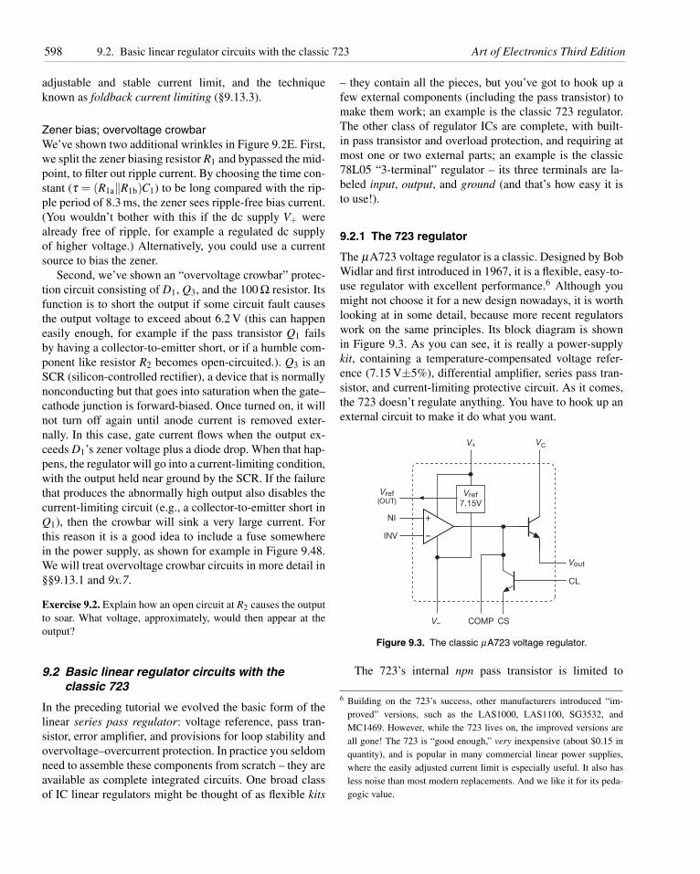
9.2.1 The 723 regulator
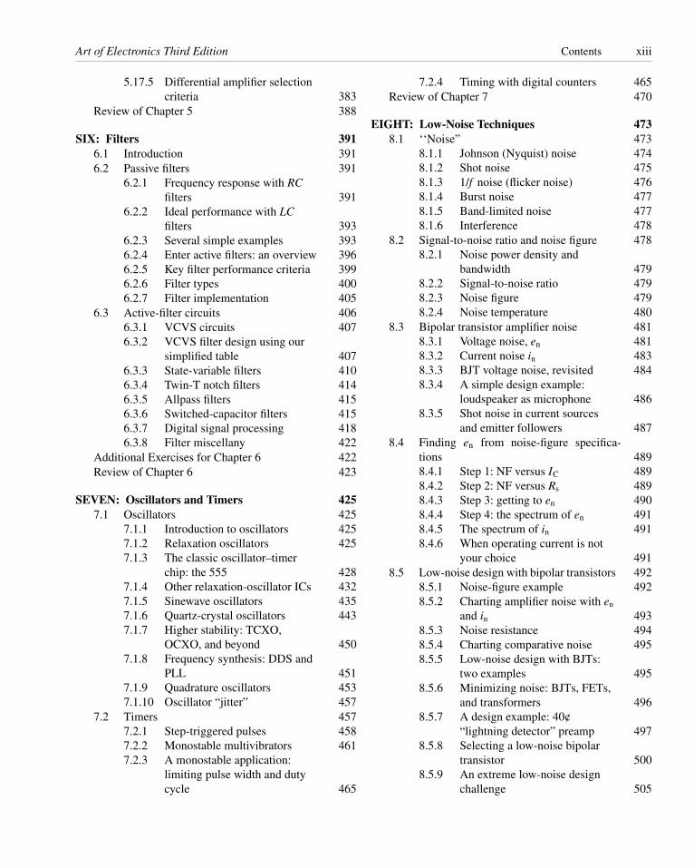
The μA723 voltage regulator is a classic. Designed by BobWidlar and first introduced in 1967, it is a flexible, easy-to-use regulator with excellent performance.6 Although youmight not choose it for a new design nowadays, it is worthlooking at in some detail, because more recent regulatorswork on the same principles. Its block diagram is shownin Figure 9.3. As you can see, it is really a power-supplykit, containing a temperature-compensated voltage refer-ence (7.15 V±5%), differential amplifier, series pass tran-sistor, and current-limiting protective circuit. As it comes,the 723 doesn’t regulate anything. You have to hook up anexternal circuit to make it do what you want.
Vref
7.15V
CL
CSCOMPV–
V+
Vref(OUT)
Vout
VC
+
–
NI
NVI
Figure 9.3. The classic μA723 voltage regulator.
The 723’s internal npn pass transistor is limited to
6 Building on the 723’s success, other manufacturers introduced “im-proved” versions, such as the LAS1000, LAS1100, SG3532, andMC1469. However, while the 723 lives on, the improved versions areall gone! The 723 is “good enough,” very inexpensive (about $0.15 inquantity), and is popular in many commercial linear power supplies,where the easily adjusted current limit is especially useful. It also hasless noise than most modern replacements. And we like it for its peda-gogic value.
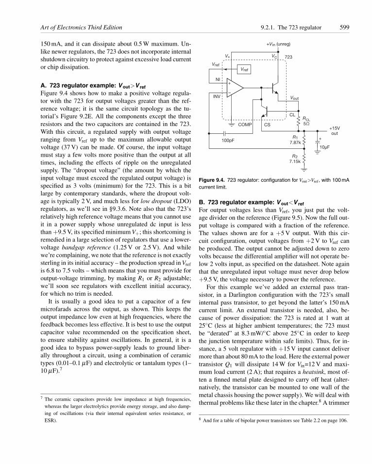
Art of Electronics Third Edition 9.2.1. The 723 regulator 599
150 mA, and it can dissipate about 0.5 W maximum. Un-like newer regulators, the 723 does not incorporate internalshutdown circuitry to protect against excessive load currentor chip dissipation.
A. 723 regulator example: V out>V refFigure 9.4 shows how to make a positive voltage regula-tor with the 723 for output voltages greater than the ref-erence voltage; it is the same circuit topology as the tu-torial’s Figure 9.2E. All the components except the threeresistors and the two capacitors are contained in the 723.With this circuit, a regulated supply with output voltageranging from Vref up to the maximum allowable outputvoltage (37 V) can be made. Of course, the input voltagemust stay a few volts more positive than the output at alltimes, including the effects of ripple on the unregulatedsupply. The “dropout voltage” (the amount by which theinput voltage must exceed the regulated output voltage) isspecified as 3 volts (minimum) for the 723. This is a bitlarge by contemporary standards, where the dropout volt-age is typically 2 V, and much less for low dropout (LDO)regulators, as we’ll see in §9.3.6. Note also that the 723’srelatively high reference voltage means that you cannot useit in a power supply whose unregulated dc input is lessthan +9.5 V, its specified minimum V+; this shortcoming isremedied in a large selection of regulators that use a lower-voltage bandgap reference (1.25 V or 2.5 V). And whilewe’re complaining, we note that the reference is not exactlysterling in its initial accuracy – the production spread in Vref
is 6.8 to 7.5 volts – which means that you must provide foroutput-voltage trimming, by making R1 or R2 adjustable;we’ll soon see regulators with excellent initial accuracy,for which no trim is needed.
It is usually a good idea to put a capacitor of a fewmicrofarads across the output, as shown. This keeps theoutput impedance low even at high frequencies, where thefeedback becomes less effective. It is best to use the outputcapacitor value recommended on the specification sheet,to ensure stability against oscillations. In general, it is agood idea to bypass power-supply leads to ground liber-ally throughout a circuit, using a combination of ceramictypes (0.01–0.1 μF) and electrolytic or tantalum types (1–10 μF).7
7 The ceramic capacitors provide low impedance at high frequencies,whereas the larger electrolytics provide energy storage, and also damp-ing of oscillations (via their internal equivalent series resistance, orESR).
+
–
Vref
Vout
RCL
5Ω
10μF
100pFR1
7.87k
R2
7.15k
Vref
+Vin (unreg)
VCV+
NI
INV
723
CL
CSCOMP+15Vout
+
Figure 9.4. 723 regulator: configuration for Vout>Vref, with 100 mAcurrent limit.
B. 723 regulator example: V out<V refFor output voltages less than Vref, you just put the volt-age divider on the reference (Figure 9.5). Now the full out-put voltage is compared with a fraction of the reference.The values shown are for a +5 V output. With this cir-cuit configuration, output voltages from +2 V to Vref canbe produced. The output cannot be adjusted down to zerovolts because the differential amplifier will not operate be-low 2 volts input, as specified on the datasheet. Note againthat the unregulated input voltage must never drop below+9.5 V, the voltage necessary to power the reference.
For this example we’ve added an external pass tran-sistor, in a Darlington configuration with the 723’s smallinternal pass transistor, to get beyond the latter’s 150 mAcurrent limit. An external transistor is needed, also, be-cause of power dissipation: the 723 is rated at 1 watt at25◦C (less at higher ambient temperatures; the 723 mustbe “derated” at 8.3 mW/◦C above 25◦C in order to keepthe junction temperature within safe limits). Thus, for in-stance, a 5 volt regulator with +15 V input cannot delivermore than about 80 mA to the load. Here the external powertransistor Q1 will dissipate 14 W for Vin=12 V and maxi-mum load current (2 A); that requires a heatsink, most of-ten a finned metal plate designed to carry off heat (alter-natively, the transistor can be mounted to one wall of themetal chassis housing the power supply). We will deal withthermal problems like these later in the chapter.8 A trimmer
8 And for a table of bipolar power transistors see Table 2.2 on page 106.
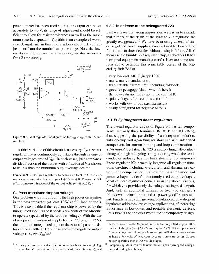
600 9.2. Basic linear regulator circuits with the classic 723 Art of Electronics Third Edition
potentiometer has been used so that the output can be setaccurately to +5 V; its range of adjustment should be suf-ficient to allow for resistor tolerances as well as the maxi-mum specified spread in Vref (this is an example of worst-case design), and in this case it allows about ±1 volt ad-justment from the nominal output voltage. Note the low-resistance high-power current-limiting resistor necessaryfor a 2 amp supply.
+
–
Vref
Vout
0.25Ω3W
Q1
TIP41
heatsink
100pF
R4 1.5k
R1
1.15k
R2
2.0k
R3
4.02k
Vref
Vadj
+Vin (unreg)
+9.5V (min)
VCV+
NI
INV
723
CL 100
CSCOMP
+5V,2A
+7.15V
10μF15V
+
Figure 9.5. 723 regulator: configuration for Vout <Vref, with 2 A cur-rent limit.
A third variation of this circuit is necessary if you want aregulator that is continuously adjustable through a range ofoutput voltages around Vref. In such cases, just compare adivided fraction of the output with a fraction of Vref chosento be less than the minimum output voltage desired.
Exercise 9.3. Design a regulator to deliver up to 50 mA load cur-rent over an output voltage range of +5 V to +10 V using a 723.Hint: compare a fraction of the output voltage with 0.5Vref.
C. Pass-transistor dropout voltageOne problem with this circuit is the high power dissipationin the pass transistor (at least 10 W at full load current).This is unavoidable if the regulator chip is powered by theunregulated input, since it needs a few volts of “headroom”to operate (specified by the dropout voltage). With the useof a separate low-current supply for the 723 (e.g., +12 V),the minimum unregulated input to the external pass transis-tor can be as little as 1.5 V or so above the regulated outputvoltage (i.e., two VBE’s).9
9 A trick you can use to reduce the minimum headroom to a single VBE
is to replace Q1 with a pnp pass transistor (tie its emitter to Vin and
9.2.2 In defense of the beleaguered 723
Lest we leave the wrong impression, we hasten to remarkthat rumors of the death of the vintage 723 regulator aregreatly exaggerated.10 We have been using dozens of lin-ear regulated power supplies manufactured by Power Onefor more than three decades without a single failure. All ofthem use the humble 723 regulator chip, as do other OEMs(“original equipment manufacturers”). Here are some rea-sons not to overlook this remarkable design of the leg-endary Bob Widlar:
• very low cost, $0.17 (in qty 1000)• many, many manufacturers• fully settable current limit, including foldback• good for pedagogy (that’s why it’s here!)• the power dissipation is not in the control IC• quiet voltage reference, plus can add filter• works with npn or pnp pass transistors• easily configured for negative outputs
9.3 Fully integrated linear regulators
The overall regulator circuit of Figure 9.5 has ten compo-nents, but only three terminals (IN, OUT, and GROUND),thus suggesting the possibility of an integrated solution,with on-chip voltage-setting resistors and with integratedcomponents for current-limiting and loop compensation –a 3-terminal regulator. The 723 is approaching half-centuryvintage (though still going strong!), during which the semi-conductor industry has not been sleeping: contemporarylinear regulator ICs generally integrate all regulator func-tions on-chip, including overcurrent and thermal protec-tion, loop compensation, high-current pass transistor, andpreset voltage divider for commonly used output voltages.Most of these regulators come also in adjustable versions,for which you provide only the voltage-setting resistor pair.And, with an additional terminal or two, you can get a“shutdown” control input and a “power-good” status out-put. Finally, a large and growing population of low-dropoutregulators addresses low voltage applications, of increasingimportance in low-power and portable electronic devices.Let’s look at the choices favored for contemporary design.
drive its base from the Vc pin of the 723), forming a Sziklai pair ratherthan a Darlington (see §2.4.2A and Figure 2.77). If the input comesfrom an unregulated dc supply, however, you will always have to allowat least a few volts of headroom, because worst-case design dictatesproper operation even at 105 Vac line input.
10 Paraphrasing Mark Twain’s famous remark, upon opening the newspa-per and reading his obituary.
Art of Electronics Third Edition 9.3.2. Three-terminal fixed regulators 601
9.3.1 Taxonomy of linear regulator ICs
As a guide to the following sections, we’ve organized theuniverse of integrated linear voltage regulators into a fewdistinct categories, here simply listed in outline form. Foreach category we’ve listed typical example part numbersof devices that we are fond of, and use often. Read on forexplanations of when and how to use them, a description oftheir distinguishing features, and some important cautions.
3-terminal fixedpos: 78xxneg: 79xx
3-terminal adjustablepos: LM317neg: LM337
3-term “lower dropout” (adj & fixed)pos: LM1117, LT1083-85
3-term fixed & 4-term adj “true LDO”pos: LT1764A/LT1963 (BJT); TPS744xx (CMOS)neg: LT1175, LM2991 (BJT); TPS7A3xxx (CMOS)
3-term current referencepos: LT3080
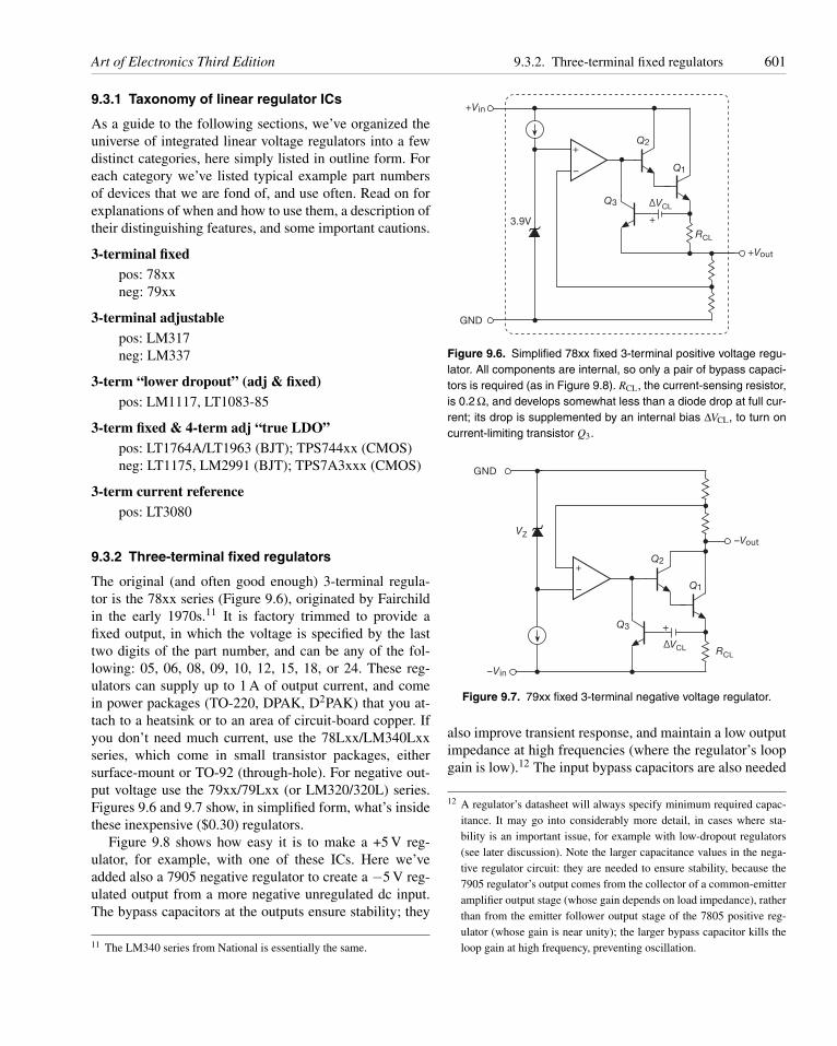
9.3.2 Three-terminal fixed regulators
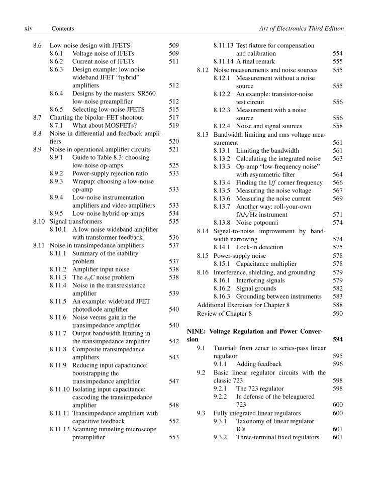
The original (and often good enough) 3-terminal regula-tor is the 78xx series (Figure 9.6), originated by Fairchildin the early 1970s.11 It is factory trimmed to provide afixed output, in which the voltage is specified by the lasttwo digits of the part number, and can be any of the fol-lowing: 05, 06, 08, 09, 10, 12, 15, 18, or 24. These reg-ulators can supply up to 1 A of output current, and comein power packages (TO-220, DPAK, D2PAK) that you at-tach to a heatsink or to an area of circuit-board copper. Ifyou don’t need much current, use the 78Lxx/LM340Lxxseries, which come in small transistor packages, eithersurface-mount or TO-92 (through-hole). For negative out-put voltage use the 79xx/79Lxx (or LM320/320L) series.Figures 9.6 and 9.7 show, in simplified form, what’s insidethese inexpensive ($0.30) regulators.
Figure 9.8 shows how easy it is to make a +5 V reg-ulator, for example, with one of these ICs. Here we’veadded also a 7905 negative regulator to create a −5 V reg-ulated output from a more negative unregulated dc input.The bypass capacitors at the outputs ensure stability; they
11 The LM340 series from National is essentially the same.
+
–
Q2
Q1
Q3
3.9V
GND
+Vout
+Vin
RCL
ΔVCL
+
Figure 9.6. Simplified 78xx fixed 3-terminal positive voltage regu-lator. All components are internal, so only a pair of bypass capaci-tors is required (as in Figure 9.8). RCL, the current-sensing resistor,is 0.2 Ω, and develops somewhat less than a diode drop at full cur-rent; its drop is supplemented by an internal bias ΔVCL, to turn oncurrent-limiting transistor Q3.
+
–
Q2
Q1
Q3
GND
–Vin
VZ
RCL
ΔVCL
–Vout
+
Figure 9.7. 79xx fixed 3-terminal negative voltage regulator.
also improve transient response, and maintain a low outputimpedance at high frequencies (where the regulator’s loopgain is low).12 The input bypass capacitors are also needed
12 A regulator’s datasheet will always specify minimum required capac-itance. It may go into considerably more detail, in cases where sta-bility is an important issue, for example with low-dropout regulators(see later discussion). Note the larger capacitance values in the nega-tive regulator circuit: they are needed to ensure stability, because the7905 regulator’s output comes from the collector of a common-emitteramplifier output stage (whose gain depends on load impedance), ratherthan from the emitter follower output stage of the 7805 positive reg-ulator (whose gain is near unity); the larger bypass capacitor kills theloop gain at high frequency, preventing oscillation.
602 9.3. Fully integrated linear regulators Art of Electronics Third Edition
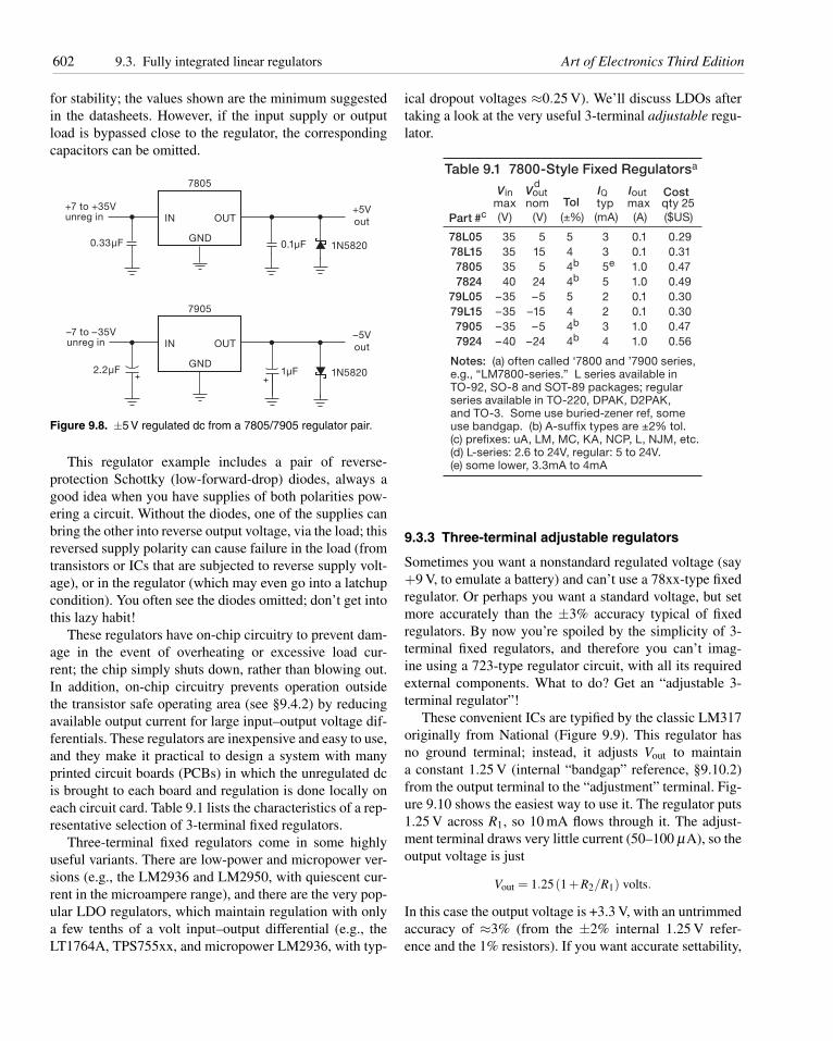
for stability; the values shown are the minimum suggestedin the datasheets. However, if the input supply or outputload is bypassed close to the regulator, the correspondingcapacitors can be omitted.
+7 to +35Vunreg in
+5V
outIN OUT
0.33μFGND
7805
1N58200.1μF
–7 to –35Vunreg in
–5V
outIN OUT
2.2μFGND
7905
1N58201μF
Figure 9.8. ±5 V regulated dc from a 7805/7905 regulator pair.
This regulator example includes a pair of reverse-protection Schottky (low-forward-drop) diodes, always agood idea when you have supplies of both polarities pow-ering a circuit. Without the diodes, one of the supplies canbring the other into reverse output voltage, via the load; thisreversed supply polarity can cause failure in the load (fromtransistors or ICs that are subjected to reverse supply volt-age), or in the regulator (which may even go into a latchupcondition). You often see the diodes omitted; don’t get intothis lazy habit!
These regulators have on-chip circuitry to prevent dam-age in the event of overheating or excessive load cur-rent; the chip simply shuts down, rather than blowing out.In addition, on-chip circuitry prevents operation outsidethe transistor safe operating area (see §9.4.2) by reducingavailable output current for large input–output voltage dif-ferentials. These regulators are inexpensive and easy to use,and they make it practical to design a system with manyprinted circuit boards (PCBs) in which the unregulated dcis brought to each board and regulation is done locally oneach circuit card. Table 9.1 lists the characteristics of a rep-resentative selection of 3-terminal fixed regulators.
Three-terminal fixed regulators come in some highlyuseful variants. There are low-power and micropower ver-sions (e.g., the LM2936 and LM2950, with quiescent cur-rent in the microampere range), and there are the very pop-ular LDO regulators, which maintain regulation with onlya few tenths of a volt input–output differential (e.g., theLT1764A, TPS755xx, and micropower LM2936, with typ-
ical dropout voltages ≈0.25 V). We’ll discuss LDOs aftertaking a look at the very useful 3-terminal adjustable regu-lator.
Vin IoutIQTol typ
Cost
(V)
max maxnom qty 25
(V) (±%) (mA) (A) ($US)
78L05
Part #c
Table 9.1 7800-Style Fixed Regulatorsa
35 5 5 3 0.1 0.29
78L15 35 15 4 3 0.1 0.31
7805 35 5 4b 5e 1.0 0.47
7824 40 24 4b 5 1.0 0.49
79L05 –35 –5 5 2 0.1 0.30
79L15 –35 –15 4 2 0.1 0.30
7905 –35 –5 4b 3 1.0 0.47
7924 –40 –24 4b 4 1.0 0.56
Notes: (a) often called ‘7800 and ’7900 series,e.g., “LM7800-series.” L series available inTO-92, SO-8 and SOT-89 packages; regularseries available in TO-220, DPAK, D2PAK,and TO-3. Some use buried-zener ref, someuse bandgap. (b) A-suffix types are ±2% tol.(c) prefixes: uA, LM, MC, KA, NCP, L, NJM, etc.(d) L-series: 2.6 to 24V, regular: 5 to 24V.(e) some lower, 3.3mA to 4mA
Voutd
9.3.3 Three-terminal adjustable regulators
Sometimes you want a nonstandard regulated voltage (say+9 V, to emulate a battery) and can’t use a 78xx-type fixedregulator. Or perhaps you want a standard voltage, but setmore accurately than the ±3% accuracy typical of fixedregulators. By now you’re spoiled by the simplicity of 3-terminal fixed regulators, and therefore you can’t imag-ine using a 723-type regulator circuit, with all its requiredexternal components. What to do? Get an “adjustable 3-terminal regulator”!
These convenient ICs are typified by the classic LM317originally from National (Figure 9.9). This regulator hasno ground terminal; instead, it adjusts Vout to maintaina constant 1.25 V (internal “bandgap” reference, §9.10.2)from the output terminal to the “adjustment” terminal. Fig-ure 9.10 shows the easiest way to use it. The regulator puts1.25 V across R1, so 10 mA flows through it. The adjust-ment terminal draws very little current (50–100 μA), so theoutput voltage is just
Vout = 1.25(1+R2/R1) volts.
In this case the output voltage is +3.3 V, with an untrimmedaccuracy of ≈3% (from the ±2% internal 1.25 V refer-ence and the 1% resistors). If you want accurate settability,
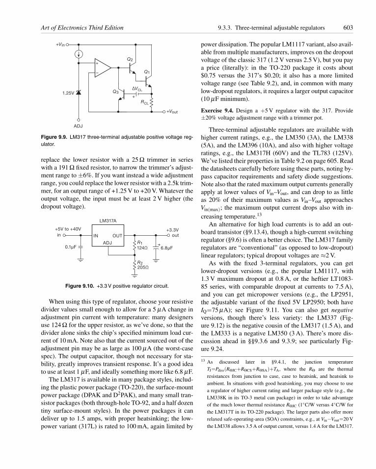
Art of Electronics Third Edition 9.3.3. Three-terminal adjustable regulators 603
+
–
Q2
Q1
Q31.25V
ADJ
+Vout
+Vin
RCL
ΔVCL
+
Figure 9.9. LM317 three-terminal adjustable positive voltage reg-ulator.
replace the lower resistor with a 25 Ω trimmer in serieswith a 191 Ω fixed resistor, to narrow the trimmer’s adjust-ment range to ±6%. If you want instead a wide adjustmentrange, you could replace the lower resistor with a 2.5k trim-mer, for an output range of +1.25 V to +20 V. Whatever theoutput voltage, the input must be at least 2 V higher (thedropout voltage).
+5V to +40V +3.3V
IN OUT
124Ω
R1
R2
0.1μF 6.8μF
205Ω
ADJ
LM317A
in out
Figure 9.10. +3.3 V positive regulator circuit.
When using this type of regulator, choose your resistivedivider values small enough to allow for a 5 μA change inadjustment pin current with temperature: many designersuse 124 Ω for the upper resistor, as we’ve done, so that thedivider alone sinks the chip’s specified minimum load cur-rent of 10 mA. Note also that the current sourced out of theadjustment pin may be as large as 100 μA (the worst-casespec). The output capacitor, though not necessary for sta-bility, greatly improves transient response. It’s a good ideato use at least 1 μF, and ideally something more like 6.8 μF.
The LM317 is available in many package styles, includ-ing the plastic power package (TO-220), the surface-mountpower package (DPAK and D2PAK), and many small tran-sistor packages (both through-hole TO-92, and a half dozentiny surface-mount styles). In the power packages it candeliver up to 1.5 amps, with proper heatsinking; the low-power variant (317L) is rated to 100 mA, again limited by
power dissipation. The popular LM1117 variant, also avail-able from multiple manufacturers, improves on the dropoutvoltage of the classic 317 (1.2 V versus 2.5 V), but you paya price (literally): in the TO-220 package it costs about$0.75 versus the 317’s $0.20; it also has a more limitedvoltage range (see Table 9.2), and, in common with manylow-dropout regulators, it requires a larger output capacitor(10 μF minimum).
Exercise 9.4. Design a +5 V regulator with the 317. Provide±20% voltage adjustment range with a trimmer pot.
Three-terminal adjustable regulators are available withhigher current ratings, e.g., the LM350 (3A), the LM338(5A), and the LM396 (10A), and also with higher voltageratings, e.g., the LM317H (60V) and the TL783 (125V).We’ve listed their properties in Table 9.2 on page 605. Readthe datasheets carefully before using these parts, noting by-pass capacitor requirements and safety diode suggestions.Note also that the rated maximum output currents generallyapply at lower values of Vin–Vout, and can drop to as littleas 20% of their maximum values as Vin–Vout approachesVin(max); the maximum output current drops also with in-creasing temperature.13
An alternative for high load currents is to add an out-board transistor (§9.13.4), though a high-current switchingregulator (§9.6) is often a better choice. The LM317 familyregulators are “conventional” (as opposed to low-dropout)linear regulators; typical dropout voltages are ≈2 V.
As with the fixed 3-terminal regulators, you can getlower-dropout versions (e.g., the popular LM1117, with1.3 V maximum dropout at 0.8 A, or the heftier LT1083-85 series, with comparable dropout at currents to 7.5 A),and you can get micropower versions (e.g., the LP2951,the adjustable variant of the fixed 5V LP2950; both haveIQ=75 μA); see Figure 9.11. You can also get negativeversions, though there’s less variety: the LM337 (Fig-ure 9.12) is the negative cousin of the LM317 (1.5 A), andthe LM333 is a negative LM350 (3 A). There’s more dis-cussion ahead in §§9.3.6 and 9.3.9; see particularly Fig-ure 9.24.
13 As discussed later in §9.4.1, the junction temperatureTJ=Pdiss(RΘJC+RΘCS+RΘSA)+TA, where the RΘ are the thermalresistances from junction to case, case to heatsink, and heatsink toambient. In situations with good heatsinking, you may choose to usea regulator of higher current rating and larger package style (e.g., theLM338K in its TO-3 metal can package) in order to take advantageof the much lower thermal resistance RΘJC (1◦C/W versus 4◦C/W forthe LM317T in its TO-220 package). The larger parts also offer morerelaxed safe-operating-area (SOA) constraints, e.g., at Vin−Vout=20 Vthe LM338 allows 3.5 A of output current, versus 1.4 A for the LM317.
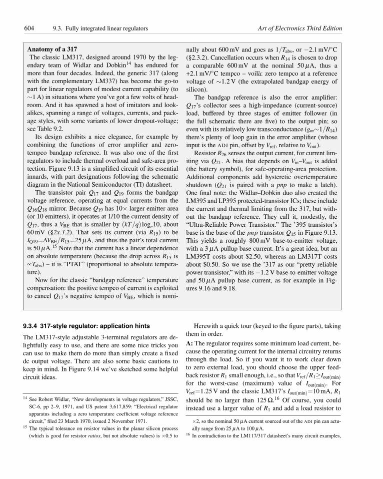
604 9.3. Fully integrated linear regulators Art of Electronics Third Edition
Anatomy of a 317The classic LM317, designed around 1970 by the leg-
endary team of Widlar and Dobkin14 has endured formore than four decades. Indeed, the generic 317 (alongwith the complementary LM337) has become the go-topart for linear regulators of modest current capability (to∼1 A) in situations where you’ve got a few volts of head-room. And it has spawned a host of imitators and look-alikes, spanning a range of voltages, currents, and pack-age styles, with some variants of lower dropout-voltage;see Table 9.2.
Its design exhibits a nice elegance, for example bycombining the functions of error amplifier and zero-tempco bandgap reference. It was also one of the firstregulators to include thermal overload and safe-area pro-tection. Figure 9.13 is a simplified circuit of its essentialinnards, with part designations following the schematicdiagram in the National Semiconductor (TI) datasheet.
The transistor pair Q17 and Q19 forms the bandgapvoltage reference, operating at equal currents from theQ16Q18 mirror. Because Q19 has 10× larger emitter area(or 10 emitters), it operates at 1/10 the current density ofQ17, thus a VBE that is smaller by (kT/q) loge10, about60 mV (§2x.3.2). That sets its current (via R15) to beIQ19=ΔVBE/R15=25 μA, and thus the pair’s total currentis 50 μA.15 Note that the current has a linear dependenceon absolute temperature (because the drop across R15 is∝Tabs) – it is “PTAT” (proportional to absolute tempera-ture).
Now for the classic “bandgap reference” temperaturecompensation: the positive tempco of current is exploitedto cancel Q17’s negative tempco of VBE, which is nomi-
nally about 600 mV and goes as 1/Tabs, or −2.1 mV/◦C(§2.3.2). Cancellation occurs when R14 is chosen to dropa comparable 600 mV at the nominal 50 μA, thus a+2.1 mV/◦C tempco – voila: zero tempco at a referencevoltage of ∼1.2 V (the extrapolated bandgap energy ofsilicon).
The bandgap reference is also the error amplifier:Q17’s collector sees a high-impedance (current-source)load, buffered by three stages of emitter follower (inthe full schematic there are five) to the output pin; soeven with its relatively low transconductance (gm∼1/R14)there’s plenty of loop gain in the error amplifier (whoseinput is the ADJ pin, offset by Vref, relative to Vout).
Resistor R26 senses the output current, for current lim-iting via Q21. A bias that depends on Vin–Vout is added(the battery symbol), for safe-operating-area protection.Additional components add hysteretic overtemperatureshutdown (Q21 is paired with a pnp to make a latch).One final note: the Widlar–Dobkin duo also created theLM395 and LP395 protected-transistor ICs; these includethe current and thermal limiting from the 317, but with-out the bandgap reference. They call it, modestly, the“Ultra-Reliable Power Transistor.” The ’395 transistor’sbase is the base of the pnp transistor Q15 in Figure 9.13.This yields a roughly 800 mV base-to-emitter voltage,with a 3 μA pullup base current. It’s a great idea, but anLM395T costs about $2.50, whereas an LM317T costsabout $0.50. So we use the ’317 as our “pretty reliablepower transistor,” with its −1.2 V base-to-emitter voltageand 50 μA pullup base current, as for example in Fig-ures 9.16 and 9.18.
9.3.4 317-style regulator: application hints
The LM317-style adjustable 3-terminal regulators are de-lightfully easy to use, and there are some nice tricks youcan use to make them do more than simply create a fixeddc output voltage. There are also some basic cautions tokeep in mind. In Figure 9.14 we’ve sketched some helpfulcircuit ideas.
14 See Robert Widlar, “New developments in voltage regulators,” JSSC,SC-6, pp 2–9, 1971, and US patent 3,617,859: “Electrical regulatorapparatus including a zero temperature coefficient voltage referencecircuit,” filed 23 March 1970, issued 2 November 1971.
15 The typical tolerance on resistor values in the planar silicon process(which is good for resistor ratios, but not absolute values) is ×0.5 to
Herewith a quick tour (keyed to the figure parts), takingthem in order.
A: The regulator requires some minimum load current, be-cause the operating current for the internal circuitry returnsthrough the load. So if you want it to work clear downto zero external load, you should choose the upper feed-back resistor R1 small enough, i.e., so that Vref/R1≥Iout(min)for the worst-case (maximum) value of Iout(min). ForVref=1.25 V and the classic LM317’s Iout(min)=10 mA, R1
should be no larger than 125 Ω.16 Of course, you couldinstead use a larger value of R1 and add a load resistor to
×2, so the nominal 50 μA current sourced out of the ADJ pin can actu-ally range from 25 μA to 100 μA.
16 In contradiction to the LM117/317 datasheet’s many circuit examples,
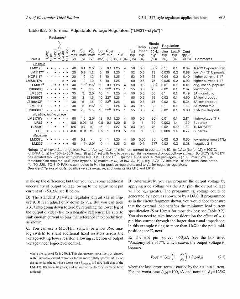
Art of Electronics Third Edition 9.3.4. 317-style regulator: application hints 605
TO
-3, T
O-3
P
Packagesz
Table 9.2. 3-Terminal Adjustable Voltage Regulators (“LM317-style”)a
Vin
Temp
Part #
120HzS
OIC
SO
T-2
23
stabc
RippleRegulation
TO
-92
TO
-220
D-P
AK
max max
hreject
Line Loade
(V)
Vref
(V)
typ
(%)
VDOmax
(V)(A)
Ioutminb
±(mA)
Coutmin
(μF)
Iadjtyp
(μA)
typ typ typ qty 25
Comments
Cost
(%) (dB) ($US)(%) (%)
PositiveLM317L 40 0.1 2.5t 5 1.25 4 50 0.5 80g 0.15 0.1 TO-92 lo-power '317
LM1117n 20 0.8 1.2 5 1.25 1 52 0.5 73 0.035 0.2 low VDO '317, popular
NCP1117 20 1.0 1.2 5 1.25 1 52 0.5 73 0.04 0.2 higher current '1117
LMS8117A 20 1.0 1.2 5 1.25 1 60 0.5 75 0.035 0.2 higher current '1117
LM317k 40 1.5p 2.5t 10 1.25 4 50 0.6 80g 0.01 0.1 orig, cheap, popular
LT1086CP 30 1.5 1.5 10 1.25 1 55 0.5 75 0.02 0.1 low dropout
LM350T 35 3 2.5t 10 1.25 4 50 0.6 65 0.1 0.1 3A monolithic
LT1085CT 30 3 1.5 10 1.25 1 55 0.5 75 0.02 0.1 3A low dropout
LT1084CP 30 5 1.5 10 1.25 1 55 0.5 75 0.02 0.1 5A low dropout
LM338T 40 5 2.5t 5 1.24 4 45 0.6 80 0.1 0.1 5A monolithic
LT1083CP 30 7.5 1.5 10 1.25 1 55 0.5 75 0.02 0.1 7.5A low dropout
Positive, high-voltageLM317HV 60 1.5 2.0t 12 1.25 4 50 0.6 80g 0.01 0.1 high-voltage '317
LR12 100 0.05 12 0.5 1.20 5 10 1 60 0.003 1.4 Supertex
Supertex
TL783C 125 0.7 10 15 1.27 5 83 0.3 76 0.02 0.15 TI, MOSFET
LR8 450 0.01 12 0.5 1.20 5 10 1 60 0.003 1.4
NegativeLM337L 40 0.1 5 1.25 4 50 0.65 80g 0.02 0.3 low-power (neg 317L)
LM337 40 1.5p 2.0t 10
0.1
10
10
10
0.1
22u
1
22u
22u
1
22u
0.1
0.1
1
1
1
1 1.25 3 65 0.6 77g 0.02 0.3
0.34
0.88
0.40
0.92
0.15
2.67
0.49
4.50
5.34
1.62
9.80
2.17
1.39
1.62
0.72
0.65
0.28 negative 317
Notes: (a) all have Vout range from Vref to Vin(max)–Vref. (b) minimum current to operate the IC. (c) ΔVout (%) for ΔTJ = 100°C.(d) D2PAK. (e) for 10% to 50% Imax. (f) at 5V. (g) with Vadj bypass cap. (h) maximum dropout voltage at Imax. (k) JRC’s NJM317Fhas isolated tab. (n) also with prefixes like TLV, LD, and REF. (p) for TO-220 and D-PAK packages. (u) 10μF min if low ESRtantalum; also requires 10μF input bypass. (v) maximum Iout at low Vin–Vout, e.g., ΔV<10V; see text. (z) the metal case or tab(for TO-220, TO-3, D-PAK) is connected to Vout for positive regulators, and to Vin for negative regulators.Beware differing pinouts: positive versus negative, and variants like LR8 and LR12.
• • - - - -
- • - • •
- - - - • •
- - - - d •
- - • • • •
- - • • - -
- - • • - -
- - • - • -
- - • • - -
- - • • - -
- - - • - -
- - • • - -
• • - • -
- - • - • -
• - - - • •
• • - - - - -
- - • • • •
Ioutv
make up the difference; but then you incur some additionaluncertainty of output voltage, owing to the adjustment pincurrent of ∼50 μA; see E below.
B: The standard 317-style regulator circuit (as in Fig-ure 9.10) can adjust only down to Vref. But you can tricka 317 into going down to zero by returning the lower leg ofthe output divider (R2) to a negative reference. Be sure tosink enough current to bias that reference into conduction,as shown.
C: You can use a MOSFET switch (or a low RON ana-log switch) to shunt additional fixed resistors across thevoltage-setting lower resistor, allowing selection of outputvoltage under logic-level control.
where the value of R1 is 240 Ω. This design error most likely originatedwith illustrative circuit examples for the more tightly spec’d LM117 onthe same datasheet, whose worst-case Iout(min) is 5 mA (half that of theLM317). It’s been 40 years, and no one at the factory seems to havenoticed!
D: Alternatively, you can program the output voltage byapplying a dc voltage via the ADJ pin; the output voltagewill be Vref greater. The programming voltage could begenerated by a pot, as shown, or by a DAC. If programmedas in the circuit fragment shown, you would need to ensurethat the external load satisfies the minimum load currentspecification (5 or 10 mA for most devices; see Table 9.2).You also need to take into consideration the effect of ADJ
pin bias current through the larger than usual impedance,in this example rising to more than 1 kΩ at the pot’s mid-position; see E, next.
E: The ADJ pin sources ∼50 μA (see the box titled“Anatomy of a 317”), which causes the output voltage tobecome
VOUT = VADJ
(1+
R2
R1
)+ IADJR2, (9.1)
where the last “error” term is caused by the ADJ pin current.For the worst-case IADJ=100 μA and nominal R1=125Ω
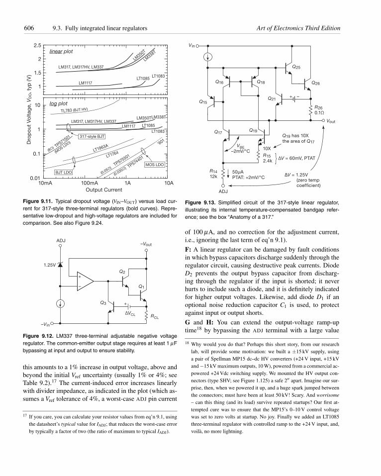
606 9.3. Fully integrated linear regulators Art of Electronics Third Edition
0.01
0.1
1
10
Dro
po
ut V
olta
ge,
VD
O, t
yp (
V)
10mA 100mA 1A 10AOutput Current
2.5
2
1.5
1
linear plot
log plot
(8Ω)
(0.05Ω)
(0.035Ω)
LM317, LM317HV, LM337
LM317, LM317HV, LM337
LM1117
LM1117
LT1083
LT1083
LT1085
LT1085
TL783 (BJT HV)
LT1764
TPS74401
LM338T
LM338T
LM350T
LM350T
LT1963ATPS71501
TPS75501
’601
MOS LDO
(MOS LDO)
BJT LDO
317-style BJT
Figure 9.11. Typical dropout voltage (VIN–VOUT) versus load cur-rent for 317-style three-terminal regulators (bold curves). Repre-sentative low-dropout and high-voltage regulators are included forcomparison. See also Figure 9.24.
+
–
Q2
Q1
Q3
ADJ
1.25V
–Vin
–Vout
RCL
ΔVCL
+
Figure 9.12. LM337 three-terminal adjustable negative voltageregulator. The common-emitter output stage requires at least 1 μFbypassing at input and output to ensure stability.
this amounts to a 1% increase in output voltage, above andbeyond the initial Vref uncertainty (usually 1% or 4%; seeTable 9.2).17 The current-induced error increases linearlywith divider impedance, as indicated in the plot (which as-sumes a Vref tolerance of 4%, a worst-case ADJ pin current
17 If you care, you can calculate your resistor values from eq’n 9.1, usingthe datasheet’s typical value for IADJ; that reduces the worst-case errorby typically a factor of two (the ratio of maximum to typical IADJ).
Q25
Q21
Q18Q16
Q15
Q17
R14
12k
ADJ
R15
2.4k } ΔV = 60mV, PTAT
Q19
Q19 has 10X
the area of Q17
10X
Q26
R26
0.1Ω
Vin
Vout
VBE
–2mV/°C
50μA
PTAT: +2mV/°C
+ –
ΔV = 1.25V (zero temp coefficient)
Figure 9.13. Simplified circuit of the 317-style linear regulator,illustrating its internal temperature-compensated bandgap refer-ence; see the box “Anatomy of a 317.”
of 100 μA, and no correction for the adjustment current,i.e., ignoring the last term of eq’n 9.1).
F: A linear regulator can be damaged by fault conditionsin which bypass capacitors discharge suddenly through theregulator circuit, causing destructive peak currents. DiodeD2 prevents the output bypass capacitor from discharg-ing through the regulator if the input is shorted; it neverhurts to include such a diode, and it is definitely indicatedfor higher output voltages. Likewise, add diode D1 if anoptional noise reduction capacitor C1 is used, to protectagainst input or output shorts.
G and H: You can extend the output-voltage ramp-uptime18 by bypassing the ADJ terminal with a large value
18 Why would you do that? Perhaps this short story, from our researchlab, will provide some motivation: we built a ±15 kV supply, usinga pair of Spellman MP15 dc–dc HV converters (+24 V input, +15 kVand −15 kV maximum outputs, 10 W), powered from a commercial ac-powered +24 Vdc switching supply. We mounted the HV output con-nectors (type SHV; see Figure 1.125) a safe 2′′ apart. Imagine our sur-prise, then, when we powered it up, and a huge spark jumped betweenthe connectors; must have been at least 50 kV! Scary. And worrisome
– can this thing (and its load) survive repeated startups? Our first at-tempted cure was to ensure that the MP15’s 0–10 V control voltagewas set to zero volts at startup. No joy. Finally we added an LT1085three-terminal regulator with controlled ramp to the +24 V input, and,voila, no more lightning.
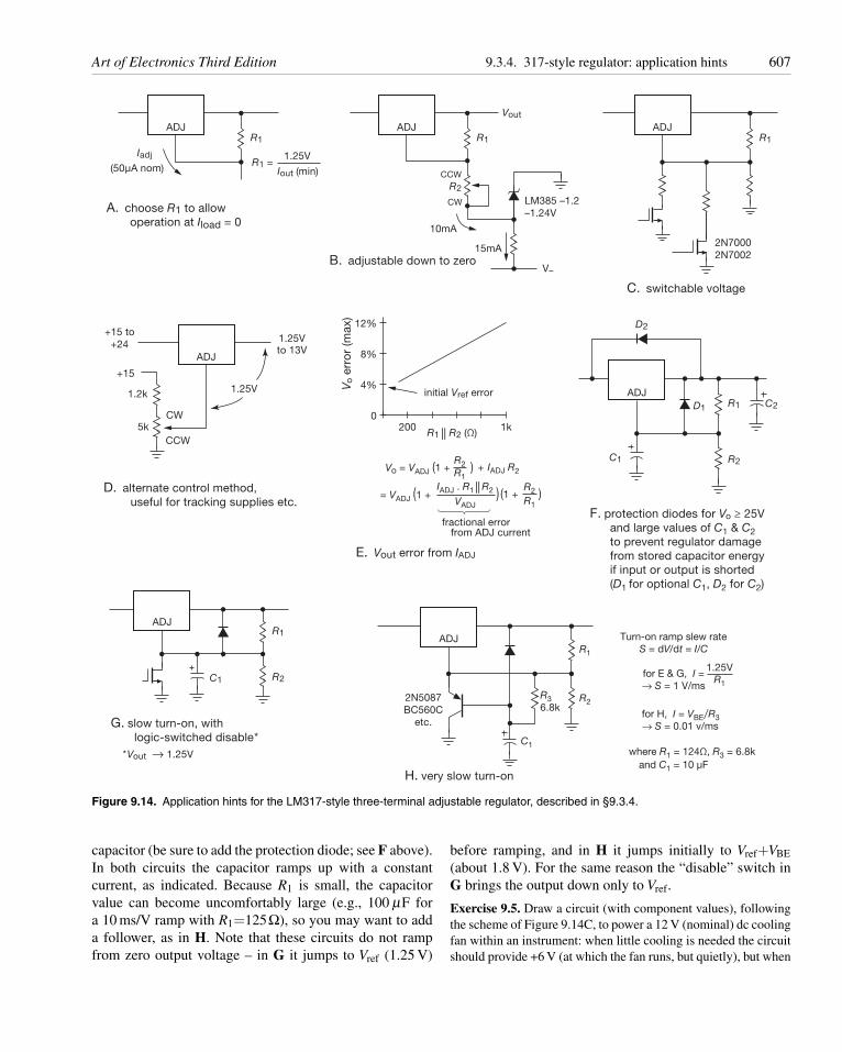
Art of Electronics Third Edition 9.3.4. 317-style regulator: application hints 607
ADJR1
A. choose R1 to allow
operation at Iload = 0
Vout
Iadj
(50μA nom)R1 =
1.25V
Iout (min)
ADJR1
CCW
R2
10mA
B. adjustable down to zero
C. switchable voltage
15mA
LM385 –1.2
–1.24V
V–
ADJ
2N7000
2N7002
R1
F. protection diodes for Vo ≥ 25V
and large values of C1 & C2
to prevent regulator damage
from stored capacitor energy
if input or output is shorted
(D1 for optional C1, D2 for C2)
ADJR1D1
D2
R2C1
C2
D. alternate control method,
useful for tracking supplies etc.
H. very slow turn-on
G. slow turn-on, with
logic-switched disable*
E. Vout error from IADJ
fractional error from ADJ current
ADJ
1.25V
1.25Vto 13V
0
4%
200 R1 || R2 (Ω)1k
V o e
rro
r (m
ax)
initial Vref error
8%
12%+15 to
+24
+15
1.2k
5kCW
CCW
ADJR1
R2C1
ADJ
2N5087
BC560C
etc.
R1
R2R3
6.8k
C1
R2
R1+Vo = VADJ (1 + ) IADJ R2
= VADJ (1 + )R2
R1
(1 + )IADJ . R1 || R2
VADJ
Turn-on ramp slew rate
S = dV/dt = I/C
for E & G, I =→ S = 1 V/ms
for H, I = VBE/R3
→ S = 0.01 v/ms
where R1 = 124Ω, R3 = 6.8k
and C1 = 10 μF
1.25V
R1
CW
*Vout → 1.25V
Figure 9.14. Application hints for the LM317-style three-terminal adjustable regulator, described in §9.3.4.
capacitor (be sure to add the protection diode; see F above).In both circuits the capacitor ramps up with a constantcurrent, as indicated. Because R1 is small, the capacitorvalue can become uncomfortably large (e.g., 100 μF fora 10 ms/V ramp with R1=125Ω), so you may want to adda follower, as in H. Note that these circuits do not rampfrom zero output voltage – in G it jumps to Vref (1.25 V)
before ramping, and in H it jumps initially to Vref+VBE
(about 1.8 V). For the same reason the “disable” switch inG brings the output down only to Vref.
Exercise 9.5. Draw a circuit (with component values), followingthe scheme of Figure 9.14C, to power a 12 V (nominal) dc coolingfan within an instrument: when little cooling is needed the circuitshould provide +6 V (at which the fan runs, but quietly), but when
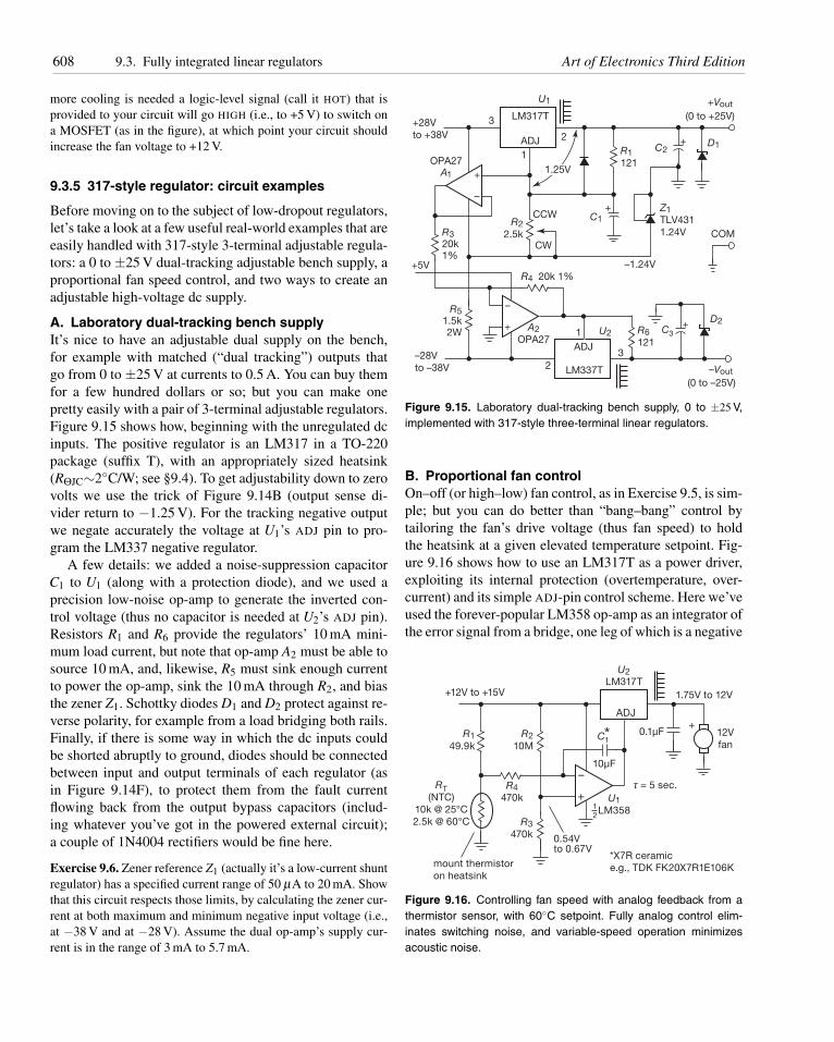
608 9.3. Fully integrated linear regulators Art of Electronics Third Edition
more cooling is needed a logic-level signal (call it HOT) that isprovided to your circuit will go HIGH (i.e., to +5 V) to switch ona MOSFET (as in the figure), at which point your circuit shouldincrease the fan voltage to +12 V.
9.3.5 317-style regulator: circuit examples
Before moving on to the subject of low-dropout regulators,let’s take a look at a few useful real-world examples that areeasily handled with 317-style 3-terminal adjustable regula-tors: a 0 to ±25 V dual-tracking adjustable bench supply, aproportional fan speed control, and two ways to create anadjustable high-voltage dc supply.
A. Laboratory dual-tracking bench supplyIt’s nice to have an adjustable dual supply on the bench,for example with matched (“dual tracking”) outputs thatgo from 0 to ±25 V at currents to 0.5 A. You can buy themfor a few hundred dollars or so; but you can make onepretty easily with a pair of 3-terminal adjustable regulators.Figure 9.15 shows how, beginning with the unregulated dcinputs. The positive regulator is an LM317 in a TO-220package (suffix T), with an appropriately sized heatsink(RΘJC∼2◦C/W; see §9.4). To get adjustability down to zerovolts we use the trick of Figure 9.14B (output sense di-vider return to −1.25 V). For the tracking negative outputwe negate accurately the voltage at U1’s ADJ pin to pro-gram the LM337 negative regulator.
A few details: we added a noise-suppression capacitorC1 to U1 (along with a protection diode), and we used aprecision low-noise op-amp to generate the inverted con-trol voltage (thus no capacitor is needed at U2’s ADJ pin).Resistors R1 and R6 provide the regulators’ 10 mA mini-mum load current, but note that op-amp A2 must be able tosource 10 mA, and, likewise, R5 must sink enough currentto power the op-amp, sink the 10 mA through R2, and biasthe zener Z1. Schottky diodes D1 and D2 protect against re-verse polarity, for example from a load bridging both rails.Finally, if there is some way in which the dc inputs couldbe shorted abruptly to ground, diodes should be connectedbetween input and output terminals of each regulator (asin Figure 9.14F), to protect them from the fault currentflowing back from the output bypass capacitors (includ-ing whatever you’ve got in the powered external circuit);a couple of 1N4004 rectifiers would be fine here.
Exercise 9.6. Zener reference Z1 (actually it’s a low-current shuntregulator) has a specified current range of 50 μA to 20 mA. Showthat this circuit respects those limits, by calculating the zener cur-rent at both maximum and minimum negative input voltage (i.e.,at −38 V and at −28 V). Assume the dual op-amp’s supply cur-rent is in the range of 3 mA to 5.7 mA.
+
–
+28V
to +38V
–28V
to –38V
–1.24V
OPA27A1
3
+
1
2
R1
121
R6
121
R2
2.5k
Z1
TLV431
1.24VR3
20k1%
R4 20k 1%
R5
1.5k2W
+5V
LM317T
ADJ
U1
U2
+
+
3
1
ADJ
2LM337T
–
+
1.25V
C2
C1
C3
D2
D1
(0 to +25V)
(0 to –25V)
CCW
COMCW
+Vout
–Vout
A2
OPA27
Figure 9.15. Laboratory dual-tracking bench supply, 0 to ±25 V,implemented with 317-style three-terminal linear regulators.
B. Proportional fan controlOn–off (or high–low) fan control, as in Exercise 9.5, is sim-ple; but you can do better than “bang–bang” control bytailoring the fan’s drive voltage (thus fan speed) to holdthe heatsink at a given elevated temperature setpoint. Fig-ure 9.16 shows how to use an LM317T as a power driver,exploiting its internal protection (overtemperature, over-current) and its simple ADJ-pin control scheme. Here we’veused the forever-popular LM358 op-amp as an integrator ofthe error signal from a bridge, one leg of which is a negative
U2
LM317T+12V to +15V
0.54Vto 0.67V
1.75V to 12V
12V
fan
0.1μF
10μF
τ = 5 sec.
+R1
49.9k
R3
470k
R2
10M
R4
470k
RT
(NTC)
10k @ 25°C
2.5k @ 60°C
mount thermistor
on heatsink
*X7R ceramic
e.g., TDK FK20X7R1E106K
C1*
ADJ
+
–
U1
LM3581
2
Figure 9.16. Controlling fan speed with analog feedback from athermistor sensor, with 60◦C setpoint. Fully analog control elim-inates switching noise, and variable-speed operation minimizesacoustic noise.
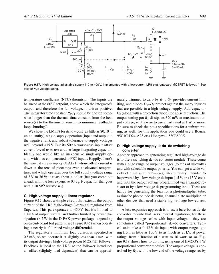
Art of Electronics Third Edition 9.3.5. 317-style regulator: circuit examples 609
SupertexLR8
IN OUT
ADJ
+Vin
Vout
0 to +400V
0 – 50mA
+415V
to +450V R1a
1.30k
CAL R1b 500
R5
100
R3
12Ω
R4
1M
1W
D1
IN4007
D3 D2
Q1
FQP5N60C
Q2
C2
C1
2.2μF
450V
20W
12V10μA
800μA
1.20V
CW
CCW+++
R2
500k
1W pot
400V *
Figure 9.17. High-voltage adjustable supply I, 0 to 400 V, implemented with a low-current LR8 plus outboard MOSFET follower. * Seetext for R2’s voltage rating.
temperature coefficient (NTC) thermistor. The inputs arebalanced at the 60◦C setpoint, above which the integrator’soutput, and therefore the fan voltage, is driven positive.The integrator time constant R4C1 should be chosen some-what longer than the thermal time constant from the heatsource(s) to the thermistor sensor, to minimize feedback-loop “hunting.”
We chose the LM358 for its low cost (as little as $0.10 inunit quantity), single-supply operation (input and output tothe negative rail), and robust tolerance to supply voltageswell beyond +15 V. But its 50 nA worst-case input offsetcurrent forced us to use a rather large integrating capacitor.Ideally one would like an inexpensive single-supply op-amp with bias-compensated or FET inputs. Happily, there’sthe unusual single-supply OPA171, whose offset current isdown in the tens of picoamps even at elevated tempera-ture, and which operates over the full supply voltage rangeof 3 V to 36 V; it costs about a dollar (but you come outahead, with the less expensive 0.47 μF capacitor that goeswith a 10 MΩ resistor R4).
C. High-voltage supply I: linear regulatorFigure 9.17 shows a simple circuit that extends the outputcurrent of the LR8 high-voltage 3-terminal regulator fromSupertex. This part operates to 450 V, but it’s limited to10 mA of output current, and further limited by power dis-sipation (∼2 W in the D-PAK power package, dependingon circuit-board foil pattern; see Figure 9.45) when operat-ing at nearly its full rated voltage differential.
The regulator’s minimum load current is specified as0.5 mA, so we operate it at slightly less than 1 mA, withits output driving a high voltage power MOSFET follower.Feedback is local to the LR8, so the follower introducesan offset (slightly load dependent) that can be approxi-
mately trimmed to zero by R1b. Q2 provides current lim-iting, and diodes D1–D3 protect against the many injuriesthat are possible in a high voltage supply. Add capacitorC2 (along with a protection diode) for noise reduction. Theoutput-setting pot R2 dissipates 320 mW at maximum out-put voltage, so it’s wise to use a part rated at 1 W or more.Be sure to check the pot’s specifications for a voltage rat-ing, as well; for this application you could use a Bourns95C1C-D24-A23 or a Honeywell 53C3500K.
D. High-voltage supply II: dc–dc switchingconverter
Another approach to generating regulated high-voltage dcis to use a switching dc–dc converter module. These comewith a huge range of output voltages (to tens of kilovolts)and with selectable output polarity. You can get a wide va-riety of these with built-in regulator circuitry, intended tobe powered by a low-voltage dc input (+5 V, or +15 V, etc.),and with the output voltage programmed via a variable re-sistor or by a low-voltage dc programming input. These arehandy for generating the bias for a photomultiplier tube,avalanche photodiode detector, channel plate multiplier, orother devices that need a stable high-voltage low-currentbias.
A less-expensive approach is to use a bare-bones dc–dcconverter module that lacks internal regulation; for thesethe output voltage scales with input voltage – they aresometimes called “proportional” dc–dc converters. Typi-cal units take a 0–12 V dc input, with output ranges go-ing from as little as 100 V to as much as 25 kV, at powerratings from a fraction of a watt to 10 watts or so. Fig-ure 9.18 shows how to do this, using one of EMCO’s 3 Wproportional converter modules. The output voltage is con-trolled by R3, with the low end of the voltage range set by
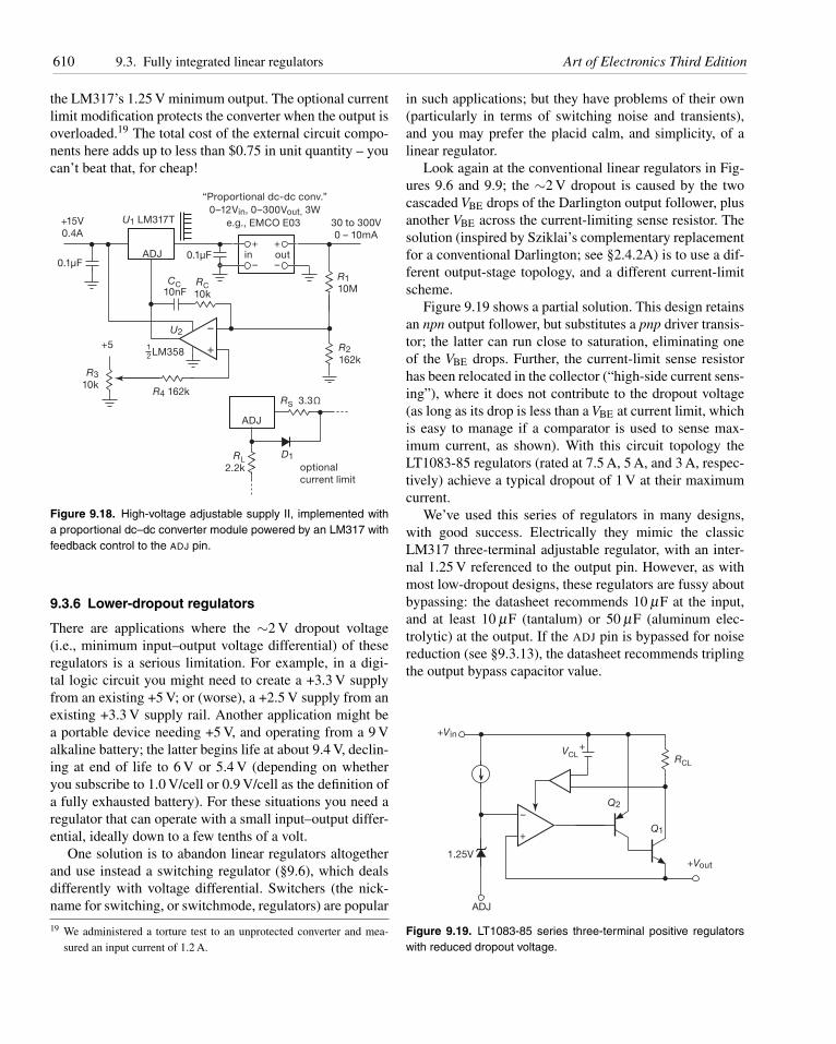
610 9.3. Fully integrated linear regulators Art of Electronics Third Edition
the LM317’s 1.25 V minimum output. The optional currentlimit modification protects the converter when the output isoverloaded.19 The total cost of the external circuit compo-nents here adds up to less than $0.75 in unit quantity – youcan’t beat that, for cheap!
U1 LM317T
“Proportional dc-dc conv.”
0–12Vin, 0–300Vout, 3W
e.g., EMCO E03 30 to 300V
0 – 10mA
R1
10M
R3
10k
10nF
D1RL
2.2k
R4 162k
R2
162k
+ +ADJ
CC RC
10k
ADJ
+15V
0.4A
0.1μF0.1μF
+5
RS 3.3Ω
optional
current limit
U2
+
–
–in out
–
LM3581
2
Figure 9.18. High-voltage adjustable supply II, implemented witha proportional dc–dc converter module powered by an LM317 withfeedback control to the ADJ pin.
9.3.6 Lower-dropout regulators
There are applications where the ∼2 V dropout voltage(i.e., minimum input–output voltage differential) of theseregulators is a serious limitation. For example, in a digi-tal logic circuit you might need to create a +3.3 V supplyfrom an existing +5 V; or (worse), a +2.5 V supply from anexisting +3.3 V supply rail. Another application might bea portable device needing +5 V, and operating from a 9 Valkaline battery; the latter begins life at about 9.4 V, declin-ing at end of life to 6 V or 5.4 V (depending on whetheryou subscribe to 1.0 V/cell or 0.9 V/cell as the definition ofa fully exhausted battery). For these situations you need aregulator that can operate with a small input–output differ-ential, ideally down to a few tenths of a volt.
One solution is to abandon linear regulators altogetherand use instead a switching regulator (§9.6), which dealsdifferently with voltage differential. Switchers (the nick-name for switching, or switchmode, regulators) are popular
19 We administered a torture test to an unprotected converter and mea-sured an input current of 1.2 A.
in such applications; but they have problems of their own(particularly in terms of switching noise and transients),and you may prefer the placid calm, and simplicity, of alinear regulator.
Look again at the conventional linear regulators in Fig-ures 9.6 and 9.9; the ∼2 V dropout is caused by the twocascaded VBE drops of the Darlington output follower, plusanother VBE across the current-limiting sense resistor. Thesolution (inspired by Sziklai’s complementary replacementfor a conventional Darlington; see §2.4.2A) is to use a dif-ferent output-stage topology, and a different current-limitscheme.
Figure 9.19 shows a partial solution. This design retainsan npn output follower, but substitutes a pnp driver transis-tor; the latter can run close to saturation, eliminating oneof the VBE drops. Further, the current-limit sense resistorhas been relocated in the collector (“high-side current sens-ing”), where it does not contribute to the dropout voltage(as long as its drop is less than a VBE at current limit, whichis easy to manage if a comparator is used to sense max-imum current, as shown). With this circuit topology theLT1083-85 regulators (rated at 7.5 A, 5 A, and 3 A, respec-tively) achieve a typical dropout of 1 V at their maximumcurrent.
We’ve used this series of regulators in many designs,with good success. Electrically they mimic the classicLM317 three-terminal adjustable regulator, with an inter-nal 1.25 V referenced to the output pin. However, as withmost low-dropout designs, these regulators are fussy aboutbypassing: the datasheet recommends 10 μF at the input,and at least 10 μF (tantalum) or 50 μF (aluminum elec-trolytic) at the output. If the ADJ pin is bypassed for noisereduction (see §9.3.13), the datasheet recommends triplingthe output bypass capacitor value.
+
+
+Vin
+Vout
1.25V
ADJ
Q1
Q2
VCL RCL
–
Figure 9.19. LT1083-85 series three-terminal positive regulatorswith reduced dropout voltage.
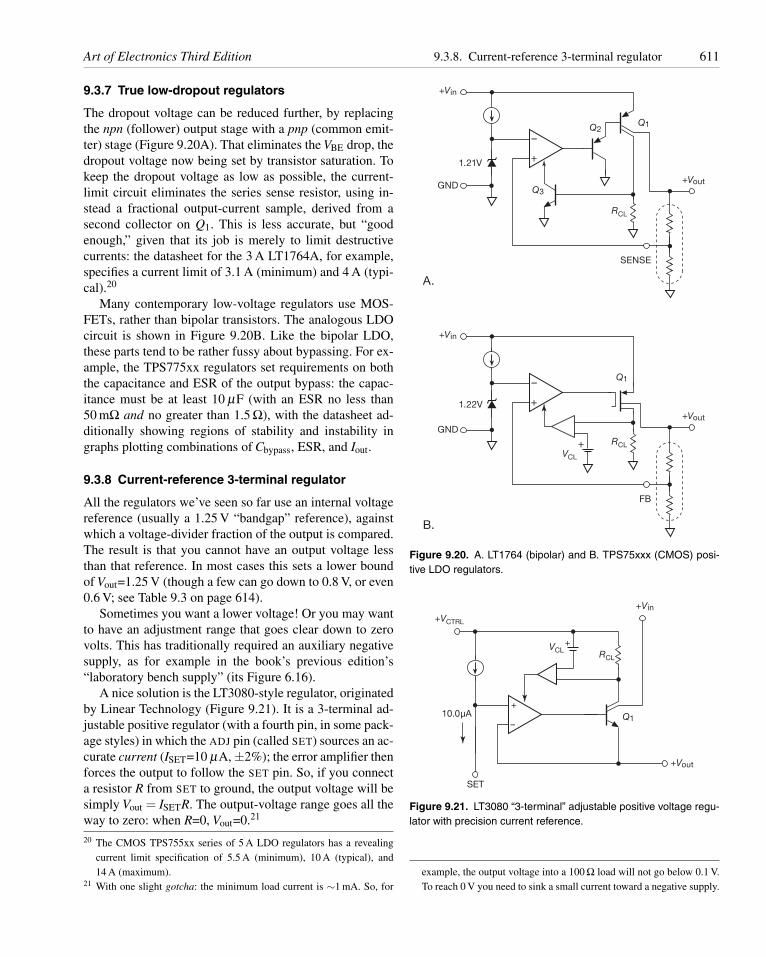
Art of Electronics Third Edition 9.3.8. Current-reference 3-terminal regulator 611
9.3.7 True low-dropout regulators
The dropout voltage can be reduced further, by replacingthe npn (follower) output stage with a pnp (common emit-ter) stage (Figure 9.20A). That eliminates the VBE drop, thedropout voltage now being set by transistor saturation. Tokeep the dropout voltage as low as possible, the current-limit circuit eliminates the series sense resistor, using in-stead a fractional output-current sample, derived from asecond collector on Q1. This is less accurate, but “goodenough,” given that its job is merely to limit destructivecurrents: the datasheet for the 3 A LT1764A, for example,specifies a current limit of 3.1 A (minimum) and 4 A (typi-cal).20
Many contemporary low-voltage regulators use MOS-FETs, rather than bipolar transistors. The analogous LDOcircuit is shown in Figure 9.20B. Like the bipolar LDO,these parts tend to be rather fussy about bypassing. For ex-ample, the TPS775xx regulators set requirements on boththe capacitance and ESR of the output bypass: the capac-itance must be at least 10 μF (with an ESR no less than50 mΩ and no greater than 1.5 Ω), with the datasheet ad-ditionally showing regions of stability and instability ingraphs plotting combinations of Cbypass, ESR, and Iout.
9.3.8 Current-reference 3-terminal regulator
All the regulators we’ve seen so far use an internal voltagereference (usually a 1.25 V “bandgap” reference), againstwhich a voltage-divider fraction of the output is compared.The result is that you cannot have an output voltage lessthan that reference. In most cases this sets a lower boundof Vout=1.25 V (though a few can go down to 0.8 V, or even0.6 V; see Table 9.3 on page 614).
Sometimes you want a lower voltage! Or you may wantto have an adjustment range that goes clear down to zerovolts. This has traditionally required an auxiliary negativesupply, as for example in the book’s previous edition’s“laboratory bench supply” (its Figure 6.16).
A nice solution is the LT3080-style regulator, originatedby Linear Technology (Figure 9.21). It is a 3-terminal ad-justable positive regulator (with a fourth pin, in some pack-age styles) in which the ADJ pin (called SET) sources an ac-curate current (ISET=10 μA, ±2%); the error amplifier thenforces the output to follow the SET pin. So, if you connecta resistor R from SET to ground, the output voltage will besimply Vout = ISETR. The output-voltage range goes all theway to zero: when R=0, Vout=0.21
20 The CMOS TPS755xx series of 5 A LDO regulators has a revealingcurrent limit specification of 5.5 A (minimum), 10 A (typical), and14 A (maximum).
21 With one slight gotcha: the minimum load current is ∼1 mA. So, for
+
–
+Vin
+Vout
1.21V
GND
A.
SENSE
Q2Q1
Q3
RCL
+
+
–
+Vin
+Vout
1.22V
GND
B.
FB
Q1
RCL
VCL
Figure 9.20. A. LT1764 (bipolar) and B. TPS75xxx (CMOS) posi-tive LDO regulators.
–
+
+VCTRL
+Vin
+Vout
10.0μA
SET
Q1
VCL RCL
+
Figure 9.21. LT3080 “3-terminal” adjustable positive voltage regu-lator with precision current reference.
example, the output voltage into a 100 Ω load will not go below 0.1 V.To reach 0 V you need to sink a small current toward a negative supply.
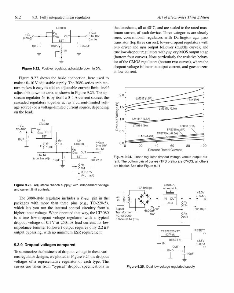
612 9.3. Fully integrated linear regulators Art of Electronics Third Edition
LT3080
+Vin
(unreg)
+Vout
0 to 10V
0 – 1A
1M
1μF 10μA+
2.2μF+
OUT
SET
VCTRL
VIN
Figure 9.22. Positive regulator, adjustable down to 0 V.
Figure 9.22 shows the basic connection, here used tomake a 0–10 V adjustable supply. The 3080-series architec-ture makes it easy to add an adjustable current limit, itselfadjustable down to zero, as shown in Figure 9.23. The up-stream regulator U1 is by itself a 0–1 A current source; thecascaded regulators together act as a current-limited volt-age source (or a voltage-limited current source, dependingon the load).
U1
LT3080
U2
LT3080
OUT
SET
+Vin
12–18V
+VOUT
0 to 10V
0 – 1A
10μF R2
1Ω
OUT
SET
R3
1M
R1
100k
0 to 1A(curr lim adj)
0 to 10V(VOUT adj)
+
10μF+
47μF+
VCTRL
VIN
VCTRL
VIN
Figure 9.23. Adjustable “bench supply,” with independent voltageand current limit controls.
The 3080-style regulator includes a VCTRL pin in thepackages with more than three pins (e.g., TO-220-5),which lets you run the internal control circuitry from ahigher input voltage. When operated that way, the LT3080is a true low-dropout voltage regulator, with a typicaldropout voltage of 0.1 V at 250 mA load current. Its lowimpedance (emitter follower) output requires only 2.2 μFoutput bypassing, with no minimum ESR requirement.
9.3.9 Dropout voltages compared
To summarize the business of dropout voltage in these vari-ous regulator designs, we plotted in Figure 9.24 the dropoutvoltages of a representative regulator of each type. Thecurves are taken from “typical” dropout specifications in
the datasheets, all at 40◦C, and are scaled to the rated max-imum current of each device. Three categories are clearlyseen: conventional regulators with Darlington npn passtransistor (top three curves); lower-dropout regulators withpnp driver and npn output follower (middle curve); andtrue low-dropout regulators with pnp or pMOS output stage(bottom four curves). Note particularly the resistive behav-ior of the CMOS regulators (bottom two curves), where thedropout voltage is linear in output current, and goes to zeroat low current.
2.0
1.5
1.0
0.5
0.0
Dro
po
ut
Vo
ltag
e (
V)
100806040200
Percent Rated Current
LM317 (1.5A)
LM317L (0.1A)
LM1117 (0.8A)
78xx (1A)
LT1084 (5A)
LT1764A (3A)
TPS755xx (5A)
LT3080 (1.1A)
TPS775xx (0.5A)
Figure 9.24. Linear regulator dropout voltage versus output cur-rent. The bottom pair of curves (TPS prefix) are CMOS; all othersare bipolar. See also Figure 9.11.
6800μF
16V
acin
+10μF
C1
R1
R2
+
10μF+
LM317AT
+ heatsink3A bridge
Signal
Transformer
PC-12-2000
6.3Vac @ 4A (rms)
IN OUT
ADJ124
205
+3.3V
0–0.5A
TPS72525KTT(D2Pak)
IN
OUT
RESET
RESET´
+2.5V
0–0.5A
GND
Figure 9.25. Dual low-voltage regulated supply.
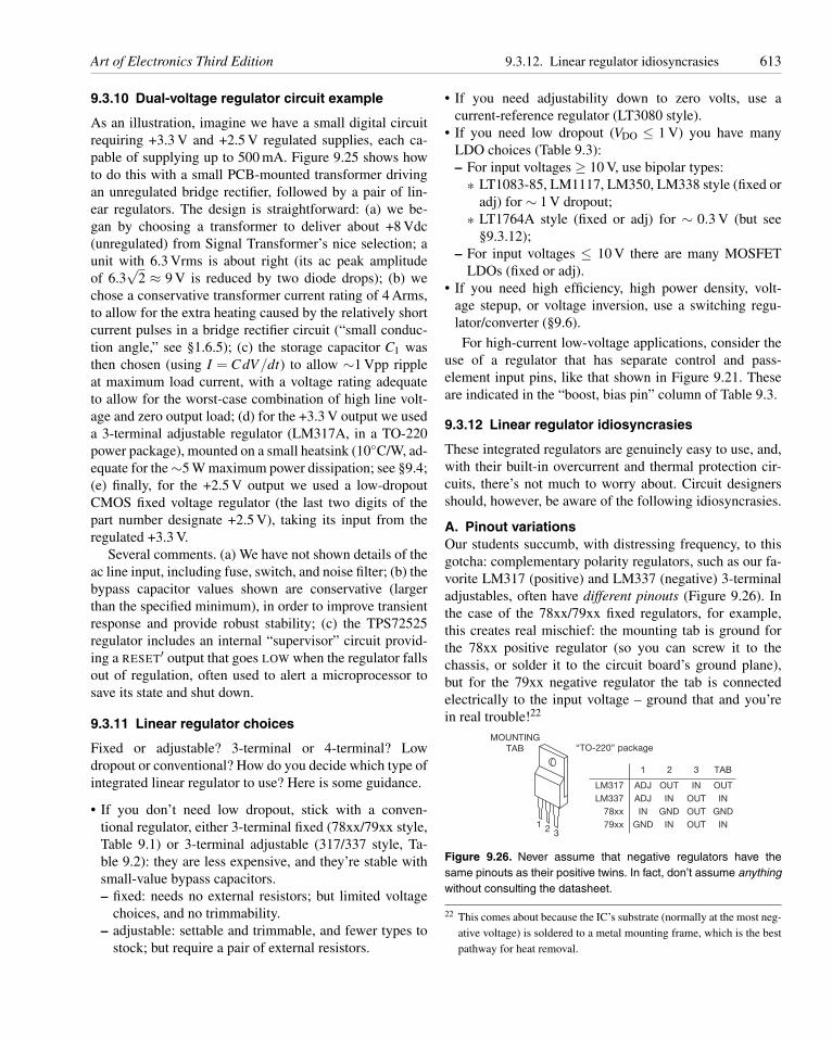
Art of Electronics Third Edition 9.3.12. Linear regulator idiosyncrasies 613
9.3.10 Dual-voltage regulator circuit example
As an illustration, imagine we have a small digital circuitrequiring +3.3 V and +2.5 V regulated supplies, each ca-pable of supplying up to 500 mA. Figure 9.25 shows howto do this with a small PCB-mounted transformer drivingan unregulated bridge rectifier, followed by a pair of lin-ear regulators. The design is straightforward: (a) we be-gan by choosing a transformer to deliver about +8 Vdc(unregulated) from Signal Transformer’s nice selection; aunit with 6.3 Vrms is about right (its ac peak amplitudeof 6.3
√2 ≈ 9 V is reduced by two diode drops); (b) we
chose a conservative transformer current rating of 4 Arms,to allow for the extra heating caused by the relatively shortcurrent pulses in a bridge rectifier circuit (“small conduc-tion angle,” see §1.6.5); (c) the storage capacitor C1 wasthen chosen (using I = C dV/dt) to allow ∼1 Vpp rippleat maximum load current, with a voltage rating adequateto allow for the worst-case combination of high line volt-age and zero output load; (d) for the +3.3 V output we useda 3-terminal adjustable regulator (LM317A, in a TO-220power package), mounted on a small heatsink (10◦C/W, ad-equate for the ∼5 W maximum power dissipation; see §9.4;(e) finally, for the +2.5 V output we used a low-dropoutCMOS fixed voltage regulator (the last two digits of thepart number designate +2.5 V), taking its input from theregulated +3.3 V.
Several comments. (a) We have not shown details of theac line input, including fuse, switch, and noise filter; (b) thebypass capacitor values shown are conservative (largerthan the specified minimum), in order to improve transientresponse and provide robust stability; (c) the TPS72525regulator includes an internal “supervisor” circuit provid-ing a RESET′ output that goes LOW when the regulator fallsout of regulation, often used to alert a microprocessor tosave its state and shut down.
9.3.11 Linear regulator choices
Fixed or adjustable? 3-terminal or 4-terminal? Lowdropout or conventional? How do you decide which type ofintegrated linear regulator to use? Here is some guidance.
• If you don’t need low dropout, stick with a conven-tional regulator, either 3-terminal fixed (78xx/79xx style,Table 9.1) or 3-terminal adjustable (317/337 style, Ta-ble 9.2): they are less expensive, and they’re stable withsmall-value bypass capacitors.– fixed: needs no external resistors; but limited voltage
choices, and no trimmability.– adjustable: settable and trimmable, and fewer types to
stock; but require a pair of external resistors.
• If you need adjustability down to zero volts, use acurrent-reference regulator (LT3080 style).
• If you need low dropout (VDO ≤ 1 V) you have manyLDO choices (Table 9.3):– For input voltages ≥ 10 V, use bipolar types:
* LT1083-85, LM1117, LM350, LM338 style (fixed oradj) for ∼ 1 V dropout;
* LT1764A style (fixed or adj) for ∼ 0.3 V (but see§9.3.12);
– For input voltages ≤ 10 V there are many MOSFETLDOs (fixed or adj).
• If you need high efficiency, high power density, volt-age stepup, or voltage inversion, use a switching regu-lator/converter (§9.6).
For high-current low-voltage applications, consider theuse of a regulator that has separate control and pass-element input pins, like that shown in Figure 9.21. Theseare indicated in the “boost, bias pin” column of Table 9.3.
9.3.12 Linear regulator idiosyncrasies
These integrated regulators are genuinely easy to use, and,with their built-in overcurrent and thermal protection cir-cuits, there’s not much to worry about. Circuit designersshould, however, be aware of the following idiosyncrasies.
A. Pinout variationsOur students succumb, with distressing frequency, to thisgotcha: complementary polarity regulators, such as our fa-vorite LM317 (positive) and LM337 (negative) 3-terminaladjustables, often have different pinouts (Figure 9.26). Inthe case of the 78xx/79xx fixed regulators, for example,this creates real mischief: the mounting tab is ground forthe 78xx positive regulator (so you can screw it to thechassis, or solder it to the circuit board’s ground plane),but for the 79xx negative regulator the tab is connectedelectrically to the input voltage – ground that and you’rein real trouble!22
MOUNTING
TAB “TO-220” package
1
1
ADJ
ADJ
IN
GND
LM317
LM337
78xx
79xx
OUT
IN
GND
IN
IN
OUT
OUT
OUT
OUT
IN
GND
IN
2 3 TAB
23
Figure 9.26. Never assume that negative regulators have thesame pinouts as their positive twins. In fact, don’t assume anythingwithout consulting the datasheet.
22 This comes about because the IC’s substrate (normally at the most neg-ative voltage) is soldered to a metal mounting frame, which is the bestpathway for heat removal.
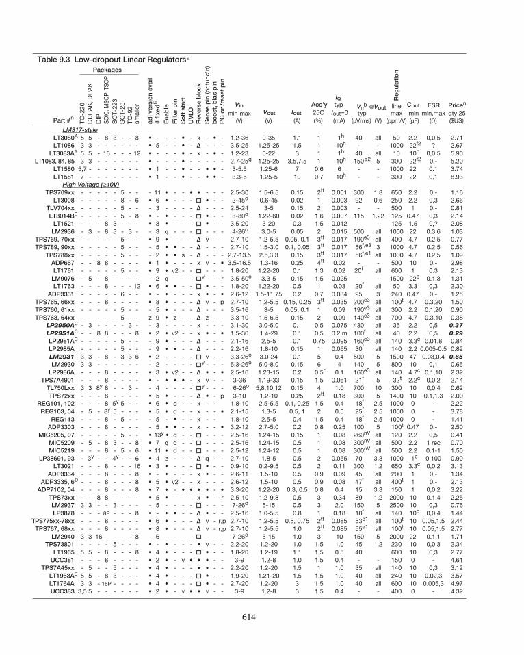
Table 9.3 Low-dropout Linear Regulatorsa
TO
-220
DD
PA
K, D
PA
K
DIP
SO
IC, M
SO
P, T
SO
P
SO
T-2
23
SO
T-2
3
TO
-92
sm
alle
r
adj v
ersi
on
avai
l#
fixed
ti
Ena
ble
Filt
er p
inS
oft
sta
rtU
VLO
Rev
erse
blo
ckS
ense
pin
(or
func’n
)
bo
ost
, bia
s p
inP
G o
r /r
eset
pin
IQVnb
Reg
ulat
ion
VinVout Iout
Acc’y typ
typline Cout ESR Pricen
min-max 25C Iout=0@Vout
max min min,max qty 25
Part #n
Packages
(V) (V) (A) (%) (mA) (μVrms) (V) (ppm/V) (μF) (Ω) ($US)
LM317-styleLT3080A 5 5 - 8 3 - - 8 • - - - • - x - • - 1.2-36 0-35 1.1 1 1h 40 all 50 2.2 0,0.5 2.71
LT1086 3 3 - - - - - - • 5 - - • - Δ - - - 3.5-25 1.25-25 1.5 1 10h - - 1000 22f2 ? 2.67
LT3083AA 5 5 - 16 - - - 12 • - - - • - x - • - 1.2-23 0-22 3 1 1h 40 all 10 10c 0,0.5 5.90
LT1083, 84, 85 3 3 - - - - - - • - - - • - - - - - 2.7-25g 1.25-25 3,5,7.5 1 10h 150e2 5 300 22f2 0,- 5.20
LT1580 5,7 - - - - - - - • 1 - - • - - • • - 3-5.5 1.25-6 7 0.6 6 - - 1000 22 0.1 3.74
LT1581 7 - - - - - - - • 1 - - • - - • • - 3.3-6 1.25-5 10 0.7 10h - - 300 22 0,1 8.93
High Voltage (≥10V)TPS709xx - - - - - 5 - - - 11 • - - • • - - - 2.5-30 1.5-6.5 0.15 2tt 0.001 300 1.8 650 2.2 0,- 1.16
LT3008 - - - - - 8 - 6 • 6 • - - - • - - 2-45o 0.6-45 0.02 1 0.003 92 0.6 250 2.2 0,3 2.66
TLV704xx - - - - - 5 - - - 3 - - - - Δ - - - 2.5-24 3-5 0.15 2 0.003 - - 500 1 0,- 0.81
LT3014BB - - - - - 5 - 8 • - • - - - • - - 3-80o 1.22-60 0.02 1.6 0.007 115 1.22 125 0.47 0,3 2.14
LT1521 - - - 8 3 - - - • 3 • - - - • - - 3.5-20 3-20 0.3 1.5 0.012 - - 125 1.5 0,? 2.08
LM2936 - 3 - 8 3 - 3 - - 3 q - - - - - - 4-26o 3.0-5 0.05 2 0.015 500 all 1000 22 0.3,6 1.03
TPS769, 70xx - - - - - 5 - - • 9 • - - - Δ v - - 2.7-10 1.2-5.5 0.05, 0.1 3tt 0.017 190e3 all 400 4.7 0.2,5 0.77
TPS789, 90xx - - - - - 5 - - - 5 • • - - Δ - - - 2.7-10 1.5-3.0 0.1, 0.05 3tt 0.017 56f,e3 3 1000 4.7 0.2,5 0.56
TPS788xx - - - - - 5 - - - 2 • • s - Δ - - - 2.7-13.5 2.5,3.3 0.15 3tt 0.017 56f,e1 all 1000 4.7 0.2,5 1.09
ADP667 - - 8 8 - - - - • 1 • - - - x v - • 3.5-16.5 1.3-16 0.25 4tt 0.02 - - 500 10 0,- 2.98
LT1761 - - - - - 5 - - • 9 • v2 - - - - - 1.8-20 1.22-20 0.1 1.3 0.02 20f all 600 1 0.3 2.13
LM9076 - 5 - 8 - - - - - 2 q - - - - - r 3.5-50o 3.3-5 0.15 1.5 0.025 - - 1500 22c 0.1,3 1.31
LT1763 - - - 8 - - - 12 • 6 • • - - • - - 1.8-20 1.22-20 0.5 1 0.03 20f all 50 3.3 0,3 2.30
ADP3331 - - - - - 6 - - • - • - - - x • - • 2.6-12 1.5-11.75 0.2 0.7 0.034 95 3 240 0.47 0,- 1.25
TPS765, 66xx - - - 8 - - - - • 8 • - - - Δ v - p 2.7-10 1.2-5.5 0.15, 0.25 3tt 0.035 200e3 all 100t 4.7 0.3,20 1.50
TPS760, 61xx - - - - - 5 - - - 5 • - - - Δ - - - 3.5-16 3-5 0.05, 0.1 1 0.09 190e3 all 300 2.2 0.1,20 0.90
TPS763, 64xx - - - - - 5 - - z 9 • z - - Δ z - - 3.3-10 1.5-6.5 0.15 2 0.09 140e3 all 700 4.7 0.3,10 0.38
LP2950AC - 3 - - - - 3 - - 3 - - - - x - - - 3.1-30 3.0-5.0 0.1 0.5 0.075 430 all 35 2.2 0,5 0.37LP2951AC - - 8 8 - - - 8 • 2 • v2 - - x • - • 1.5-30 1.4-29 0.1 0.5 0.2 m 100f all 40 2.2 0,5 0.29LP2981AC - - - - - 5 - - - 9 • - - - Δ - - - 2.1-16 2.5-5 0.1 0.75 0.095 160e3 all 140 3.3c 0.01,8 0.84
LP2985A - - - - - 5 - - - 9 • • - - Δ - - - 2.2-16 1.8-10 0.15 1 0.065 30f all 140 2.2 0.005-0.5 0.82
LM2931 3 3 - 8 - 3 3 6 • 2 - - - - v - - 3.3-26o 3.0-24 0.1 5 0.4 500 5 1500 47 0.03,0.4 0.65LM2930 3 3 - - - - - - - 2 - - - - - - - 5.3-26o 5.0-8.0 0.15 6 4 140 5 800 10 0,1 0.65
LP2986A - - - 8 - - - - • 3 • v2 - - Δ • - • 2.5-16 1.23-15 0.2 0.5d 0.1 160e3 all 140 4.7c 0.1,10 2.32
TPS7A4901 - - - 8 - - - - • - • • • - x v - - 3-36 1.19-33 0.15 1.5 0.061 21f 5 32t 2.2c 0,0.2 2.14
TL750Lxx 3 3 8y 8 - - 3 - - 4 - - - - - - - 6-26o 5,8,10,12 0.15 4 1.0 700 10 300 10 0,0.4 0.62
TPS72xx - - - 8 - - - - • 5 • - - - Δ • - p 3-10 1.2-10 0.25 2tt 0.18 300 5 1400 10 0.1,1.3 2.00
REG101, 102 - - - 8 5y 5 - - • 6 • d - - x - - 1.8-10 2.5-5.5 0.1, 0.25 1.5 0.4 18f 2.5 1000 0 - 2.22
REG103, 04 - 5 - 8y 5 - - - • 5 • d - - x - - • 2.1-15 1.3-5 0.5, 1 2 0.5 25f 2.5 1000 0 - 3.78
REG113 - - - 8 - 5 - - - 5 - • - - x - - 1.8-10 2.5-5 0.4 1.5 0.4 18f 2.5 1000 0 - 1.41
ADP3303 - - - 8 - - - - - 5 • • - - x - - • 3.2-12 2.7-5.0 0.2 0.8 0.25 100 5 100t 0.47 0,- 2.50
MIC5205, 07 - - - - - 5 - - • 13y • d - - - - - 2.5-16 1.24-15 0.15 1 0.08 260nV all 120 2.2 0,5 0.41
MIC5209 - 5 - 8 3 - - 8 • 7 q d - - - - - 2.5-16 1.24-15 0.5 1 0.08 300nV all 500 2.2 1 rec 0.70
MIC5219 - - - 8 - 5 - 6 • 11 • d - - - - - 2.5-12 1.24-12 0.5 1 0.08 300nV all 500 2.2 0.1-1 1.50
LP38691, 93 - 3y - - 4y - - 6 • 4 z - - - Δ q - - 2.7-10 1.8-5 0.5 2 0.055 70 3.3 1000 1c 0,100 0.90
LT3021 - - - 8 - - - 16 • 3 • - - - • - - 0.9-10 0.2-9.5 0.5 2 0.11 300 1.2 650 3.3c 0,0.2 3.13
ADP3334 - - - 8 - - - 8 • - • - - - x • - - 2.6-11 1.5-10 0.5 0.9 0.09 45 all 200 1 0,- 1.34
ADP3335, 6D - - - 8 - - - 8 • 5 • v2 - - x - - - 2.6-12 1.5-10 0.5 0.9 0.08 47f all 400t 1 0,- 2.13
ADP7102, 04 - - - 8 - - - 8 • 7 • - • • • • - • 3.3-20 1.22-20 0.3, 0.5 0.8 0.4 15 3.3 150 1 0,0.2 3.22
TPS73xx - - 8 8 - - - - • 5 • - - - x • - r 2.5-10 1.2-9.8 0.5 3 0.34 89 1.2 2000 10 0.1,4 2.25
LM2937 3 3 - - 3 - - - - 5 - - - - - - - 7-26o 5-15 0.5 3 2.0 150 5 2500 10 0,3 0.76
LP3878 - - - 8P - - - 8 • - • • - - Δ • - - 2.5-16 1.0-5.5 0.8 1 0.18 18f all 140 10c 0,0.4 1.44
TPS775xx-78xx - - - 8 - - - - • 6 • - - - Δ v - r,p 2.7-10 1.2-5.5 0.5, 0.75 2tt 0.085 53e1 all 100t 10 0.05,1.5 2.44
TPS767, 68xx - - - 8 - - - - • 8 • - - - Δ v - r,p 2.7-10 1.2-5.5 1.0 2tt 0.085 55e1 all 100t 10 0.05,1.5 2.77
LM2940 3 3 16 - - - - 8 - 6 - - - - - - - 7-26o 5-15 1.0 3 10 150 5 2000 22 0.1,1 1.71
TPS73801 - - - - 5 - - - • - • - - - • v - - 2.2-20 1.2-20 1.0 1.5 1.0 45 1.2 10 0,0.3 2.34
LT1965 5 5 - 8 - - - 8 • 4 • - - - • - - 1.8-20 1.2-19 1.1 1.5 0.5 40 600
230
10 0,3 2.77
UCC381 - - - 8 - - - - • 2 • - v • • • - - 3-9 1.2-8 1.0 1.5 0.4 - - 150 0 - 4.61
TPS7A45xx - 5 - - 5 - - - • 4 • - - - • • - - 2.2-20 1.2-20 1.5 1 1.0 35 all 140 10 0,3 3.12
LT1963AE 5 5 - 8 3 - - - • 4 • - - - • - - 1.9-20 1.21-20 1.5 1.5 1.0 40 all 240 10 0.02,3 3.57
LT1764A 3 3 - 16P - - - - • 4 • - - - • - - 2.7-20 1.2-20 3 1.5 1.0 40 all 600 10 0.005,3 4.97
UCC383 3,5 5 - - - - - - • 2 • - v • • v - - 3-9 1.2-8 3 1.5 0.4 - - 400 0 - 4.32
y
y
y
614
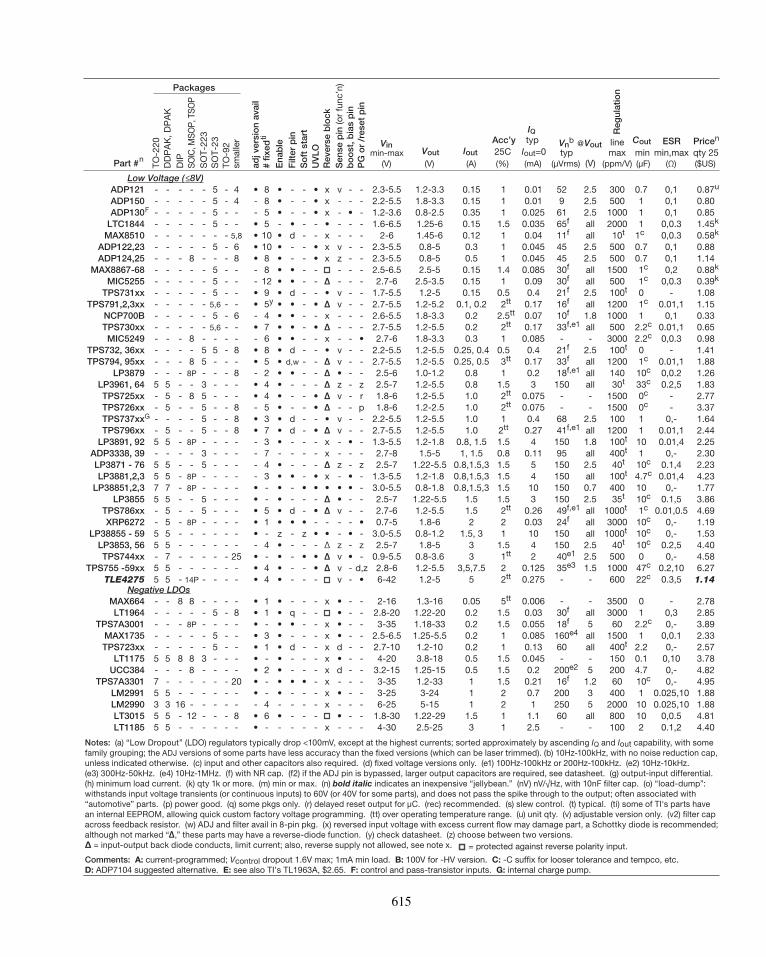
Low Voltage (≤8V)ADP121 - - - - - 5 - 4 • 8 • - - • x v - - 2.3-5.5 1.2-3.3 0.15 1 0.01 52 2.5 300 0.7 0,1 0.87u
ADP150 - - - - - 5 - 4 - 8 • - - • x - - - 2.2-5.5 1.8-3.3 0.15 1 0.01 9 2.5 500 1 0,1 0.80ADP130F - - - - - 5 - - - 5 • - - • x - • - 1.2-3.6 0.8-2.5 0.35 1 0.025 61 2.5 1000 1 0,1 0.85
LTC1844 - - - - - 5 - - • 5 - • - - • - - - 1.6-6.5 1.25-6 0.15 1.5 0.035 65f all 2000 1 0,0.3 1.45k
MAX8510 - - - - - - - 5,8 • 10 • d - - x - - - 2-6 1.45-6 0.12 1 0.04 11f all 10t 1c 0,0.3 0.58k
ADP122,23 - - - - - 5 - 6 • 10 • - - • x v - - 2.3-5.5 0.8-5 0.3 1 0.045 45 2.5 500 0.7 0,1 0.88ADP124,25 - - - 8 - - - 8 • 8 • - - • x z - - 2.3-5.5 0.8-5 0.5 1 0.045 45 2.5 500 0.7 0,1 1.14
MAX8867-68 - - - - - 5 - - - 8 • • - - - - - 2.5-6.5 2.5-5 0.15 1.4 0.085 30f all 1500 1c 0,2 0.88k
MIC5255 - - - - - 5 - - - 12 • • - - Δ - - - 2.7-6 2.5-3.5 0.15 1 0.09 30f all 500 1c 0,0.3 0.39k
TPS731xx - - - - - 5 - - • 9 ••
d - - • v - - 1.7-5.5 1.2-5 0.15 0.5 0.4 21f 2.5 100t 0 - 1.08TPS791,2,3xx - - - - - 5,6 - - • 5y • - • Δ v - - 2.7-5.5 1.2-5.2 0.1, 0.2 2tt 0.17 16f all 1200 1c 0.01,1 1.15
NCP700B - - - - - 5 - 6 - 4 • • - - x - - - 2.6-5.5 1.8-3.3 0.2 2.5tt 0.07 10f 1.8 1000 1 0,1 0.33TPS730xx - - - - - 5,6 - - • 7 • • - • Δ - - - 2.7-5.5 1.2-5.5 0.2 2tt 0.17 33f,e1 all 500 2.2c 0.01,1 0.65MIC5249 - - - 8 - - - - - 6 • • - - x - - • 2.7-6 1.8-3.3 0.3 1 0.085 - - 3000 2.2c 0,0.3 0.98
TPS732, 36xx - - - - 5 5 - 8 • 8 • d - - • v - - 2.2-5.5 1.2-5.5 0.25, 0.4 0.5 0.4 21f 2.5 100t 0 - 1.41TPS794, 95xx - - - 8 5 - - - • 5 • d,w - - Δ v - - 2.7-5.5 1.2-5.5 0.25, 0.5 3tt 0.17 33f all 1200 1c 0.01,1 1.88
LP3879 - - - 8P - - - 8 - 2 • • - - Δ • - - 2.5-6 1.0-1.2 0.8 1 0.2 18f,e1 all 140 10c 0,0.2 1.26LP3961, 64 5 5 - - 3 - - - • 4 • - - - Δ z - z 2.5-7 1.2-5.5 0.8 1.5 3 150 all 30t 33c 0.2,5 1.83TPS725xx - 5 - 8 5 - - - • 4 • - - • Δ v - r 1.8-6 1.2-5.5 1.0 2tt 0.075 - - 1500 0c - 2.77TPS726xx - 5 - - 5 - - 8 - 5 • - - • Δ - - p 1.8-6 1.2-2.5 1.0 2tt 0.075 - - 1500 0c - 3.37TPS737xxG - - - - 5 - - 8 • 3 • d - - • v - - 2.2-5.5 1.2-5.5 1.0 1 0.4 68 2.5 100 1 0,- 1.64TPS796xx - 5 - - 5 - - 8 • 7 • d - • Δ v - - 2.7-5.5 1.2-5.5 1.0 2tt 0.27 41f,e1 all 1200 1 0.01,1 2.44
LP3891, 92 5 5 - 8P - - - - - 3 • - - - x - • - 1.3-5.5 1.2-1.8 0.8, 1.5 1.5 4 150 1.8 100t 10 0.01,4 2.25ADP3338, 39 - - - - 3 - - - - 7 - - - - x - - - 2.7-8 1.5-5 1, 1.5 0.8 0.11 95 all 400t 1 0,- 2.30LP3871 - 76 5 5 - - 5 - - - - 4 • - - - Δ z - z 2.5-7 1.22-5.5 0.8,1.5,3 1.5 5 150 2.5 40t 10c 0.1,4 2.23LP3881,2,3 5 5 - 8P - - - - - 3 • • - • x - • - 1.3-5.5 1.2-1.8 0.8,1.5,3 1.5 4 150 all 100t 4.7c 0.01,4 4.23
LP38851,2,3 7 7 - 8P - - - - • - • - • • • • • - 3.0-5.5 0.8-1.8 0.8,1.5,3 1.5 10 150 0.7 400 10 0,- 1.77LP3855 5 5 - - 5 - - - • - • - - - Δ • - - 2.5-7 1.22-5.5 1.5 1.5 3 150 2.5 35t 10c 0.1,5 3.86
TPS786xx - 5 - - 5 - - - • 5 • d - • Δ v - - 2.7-6 1.2-5.5 1.5 2tt 0.26 49f,e1 all 1000t 1c 0.01,0.5 4.69XRP6272 - 5 - 8P - - - - • 1 • • • - - - - • 0.7-5 1.8-6 2 2 0.03 24f all 3000 10c 0,- 1.19
LP38855 - 59 5 5 - - - - - - • - z - z • • - • - 3.0-5.5 0.8-1.2 1.5, 3 1 10 150 all 1000t 10c 0,- 1.53LP3853, 56 5 5 - - - - - - - 4 • - - - Δ z - z 2.5-7 1.8-5 3 1.5 4 150 2.5 40t 10c 0.2,5 4.40TPS744xx - 7 - - - - - 25 • - • - • • Δ v • - 0.9-5.5 0.8-3.6 3 1tt 2 40e1 2.5 500 0 0,- 4.58
TPS755 -59xx 5 5 - - - - - - • 4 • - - • Δ v - d,z 2.8-6 1.2-5.5 3,5,7.5 2 0.125 35e3 1.5 1000 47c 0.2,10 6.27TLE4275 5 5 - 14P - - - - • 4 • - - - v - • 6-42 1.2-5 5 2tt 0.275 - - 600 22c 0.3,5 1.14
Negative LDOsMAX664 - - 8 8 - - - - • 1 • - - - x • - - 2-16 1.3-16 0.05 5tt 0.006 - - 3500 0 - 2.78LT1964 - - - - - 5 - 8 • 1 • q - - • - - 2.8-20 1.22-20 0.2 1.5 0.03 30f all 3000 1 0,3 2.85
TPS7A3001 - - - 8P - - - - • - • • - - x • - - 3-35 1.18-33 0.2 1.5 0.055 18f 5 60 2.2c 0,- 3.89MAX1735 - - - - - 5 - - • 3 • - - - x • - - 2.5-6.5 1.25-5.5 0.2 1 0.085 160e4 all 1500 1 0,0.1 2.33TPS723xx - - - - - 5 - - • 1 • d - - x d - - 2.7-10 1.2-10 0.2 1 0.13 60 all 400t 2.2 0,- 2.57
LT1175 5 5 8 8 3 - - - • - • - - - x • - - 4-20 3.8-18 0.5 1.5 0.045 - - 150 0.1 0,10 3.78UCC384 - - - 8 - - - - • 2 • - - - x d - - 3.2-15 1.25-15 0.5 1.5 0.2 200e2 5 200 4.7 0,- 4.82
TPS7A3301 7 - - - - - - 20 • - • • • - x - - - 3-35 1.2-33 1 1.5 0.21 16f 1.2 60 10c 0,- 4.95LM2991 5 5 - - - - - - • - • - - - x • - - 3-25 3-24 1 2 0.7 200 3 400 1 0.025,10 1.88LM2990 3 3 16 - - - - - - 4 - - - - x - - - 6-25 5-15 1 2 1 250 5 2000 10 0.025,10 1.88LT3015 5 5 - 12 - - - 8 • 6 • - - - • - - 1.8-30 1.22-29 1.5 1 1.1 60 all 800 10 0,0.5 4.81LT1185 5 5 - - - - - - • - - - - - x - - - 4-30 2.5-25 3 1 2.5 - - 100 2 0.1,2 4.40
Notes: (a) “Low Dropout” (LDO) regulators typically drop <100mV, except at the highest currents; sorted approximately by ascending IQ and Iout capability, with somefamily grouping; the ADJ versions of some parts have less accuracy than the fixed versions (which can be laser trimmed). (b) 10Hz-100kHz, with no noise reduction cap,unless indicated otherwise. (c) input and other capacitors also required. (d) fixed voltage versions only. (e1) 100Hz-100kHz or 200Hz-100kHz. (e2) 10Hz-10kHz.(e3) 300Hz-50kHz. (e4) 10Hz-1MHz. (f) with NR cap. (f2) if the ADJ pin is bypassed, larger output capacitors are required, see datasheet. (g) output-input differential.(h) minimum load current. (k) qty 1k or more. (m) min or max. (n) bold italic indicates an inexpensive “jellybean.” (nV) nV/√Hz, with 10nF filter cap. (o) “load-dump”:withstands input voltage transients (or continuous inputs) to 60V (or 40V for some parts), and does not pass the spike through to the output; often associated with“automotive” parts. (p) power good. (q) some pkgs only. (r) delayed reset output for μC. (rec) recommended. (s) slew control. (t) typical. (ti) some of TI's parts havean internal EEPROM, allowing quick custom factory voltage programming. (tt) over operating temperature range. (u) unit qty. (v) adjustable version only. (v2) filter capacross feedback resistor. (w) ADJ and filter avail in 8-pin pkg. (x) reversed input voltage with excess current flow may damage part, a Schottky diode is recommended;although not marked “Δ,” these parts may have a reverse-diode function. (y) check datasheet. (z) choose between two versions.Δ = input-output back diode conducts, limit current; also, reverse supply not allowed, see note x.
TO-2
20D
DP
AK
, DP
AK
DIP
SOIC
, MSO
P, T
SOP
SO
T-22
3S
OT-
23TO
-92
smal
ler
adj v
ersi
on
avai
l#
fixed
ti
Ena
ble
Filt
er p
inS
oft
sta
rtU
VLO
Rev
erse
blo
ckS
ense
pin
(or
func
’n)
bo
ost
, bia
s p
inP
G o
r /r
eset
pin
IQVnb
Reg
ulat
ion
VinVout Iout
Acc’y typtyp
line Cout ESR Pricen
min-max 25C Iout=0@Vout
max min min,max qty 25Part #n (V) (V) (A) (%) (mA) (μVrms) (V) (ppm/V) (μF) (Ω) ($US)
= protected against reverse polarity input.
Comments: A: current-programmed; Vcontrol dropout 1.6V max; 1mA min load. B: 100V for -HV version. C: -C suffix for looser tolerance and tempco, etc.D: ADP7104 suggested alternative. E: see also TI’s TL1963A, $2.65. F: control and pass-transistor inputs. G: internal charge pump.
Packages
615
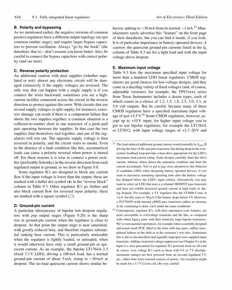
616 9.3. Fully integrated linear regulators Art of Electronics Third Edition
B. Polarity and bypassingAs we mentioned earlier, the negative versions of commonpositive regulators have a different output topology (an npncommon emitter stage), and require larger bypass capaci-tors to prevent oscillation. Always “go by the book” (thedatasheet, that is) – don’t assume you know better. Also, becareful to connect the bypass capacitors with correct polar-ity (and see next).
C. Reverse polarity protectionAn additional caution with dual supplies (whether regu-lated or not): almost any electronic circuit will be dam-aged extensively if the supply voltages are reversed. Theonly way that can happen with a single supply is if youconnect the wires backward; sometimes you see a high-current rectifier connected across the circuit in the reversedirection to protect against this error. With circuits that useseveral supply voltages (a split supply, for instance), exten-sive damage can result if there is a component failure thatshorts the two supplies together; a common situation is acollector-to-emitter short in one transistor of a push–pullpair operating between the supplies. In that case the twosupplies find themselves tied together, and one of the reg-ulators will win out. The opposite supply voltage is thenreversed in polarity, and the circuit starts to smoke. Evenin the absence of a fault condition like this, asymmetricalloads can cause a polarity reversal when power is turnedoff. For these reasons it is wise to connect a power recti-fier (preferably Schottky) in the reverse direction from eachregulated output to ground, as we drew in Figure 9.8.
Some regulator ICs are designed to block any currentflow if the input voltage is lower than the output; these aremarked with a bullet dot symbol (•) in the “reverse block”column in Table 9.3. Other regulator ICs go further andalso block current flow for reversed input polarity; theseare marked with a square symbol (�).
D. Ground-pin currentA particular idiosyncrasy of bipolar low-dropout regula-tors with pnp output stages (Figure 9.20) is the sharprise in ground-pin current when the regulator is close todropout. At that point the output stage is near saturation,with greatly reduced beta, and therefore requires substan-tial sinking base current. This is particularly noticeablewhen the regulator is lightly loaded, or unloaded, whenit would otherwise have only a small ground-pin or qui-escent current. As an example, the bipolar LT1764A-3.3(fixed 3.3 V LDO), driving a 100 mA load, has a normalground-pin current of about 5 mA, rising to ∼50 mA atdropout. The no-load quiescent current shows similar be-
havior, spiking to ∼30 mA from its normal ∼1 mA.23 Man-ufacturers rarely advertise this “feature” on the front pageof their datasheets, but you can find it inside, if you look.It is of particular importance in battery-operated devices. Acaution: the quiescent ground-pin currents listed in the IQ
column of Table 9.3 are for a light load and with the inputvoltage above dropout.
E. Maximum input voltageTable 9.3 lists the maximum specified input voltage formore than a hundred LDO linear regulators. CMOS reg-ulators are good choices for low-voltage designs, and theycome in a dazzling variety of fixed voltages (and, of course,adjustable versions): for example, the TPS7xxxx seriesfrom Texas Instruments includes a dozen types, each ofwhich comes in a choice of 1.2, 1.5, 1.8, 2.5, 3.0, 3.3, or5.0 volt outputs. But be careful, because many of theseCMOS regulators have a specified maximum input volt-age of just +5.5 V.24 Some CMOS regulators, however, ac-cept up to +10 V input; for higher input voltage you’vegot to use bipolar regulators, for example the LT1764Aor LT3012, with input voltage ranges of +2.7–20 V and
23 The load-induced additional ground current would normally be Iload/βdriving the base of the pnp pass transistor, but during dropout the ever-zealous feedback loop provides a base drive appropriate for the LDO’smaximum load-current rating. Some designs carefully limit this drivecurrent, whereas others detect the saturation condition and limit thecurrent accordingly. You’ve got to pay close attention to this behaviorof candidate LDOs when designing battery operated devices, if youwant to maximize remaining operating time after the battery voltagehas dropped below the LDO’s input criteria. Alternatively you maywant to select an LDO that uses a p-channel MOSFET pass transistorand does not exhibit increased ground current at high loads or dur-ing dropout. For example, a 5 V regulator like the LT3008-5 runs at3 μA, but this soars to 30 μA if the battery drops below 5 V. However,a TLV70450 (with internal pMOS pass transistor) suffers no increaseat all, continuing to draw 3 μA under the same conditions.
24 Contemporary regulator ICs, with their nanometer-scale features, aremore susceptible to overvoltage transients and the like, as comparedwith robust legacy parts with their relatively large bipolar transistors.We’ve seen painful experiences, for example when a carefully designedand tested small PCB, filled to the brim with tiny parts, suffers unex-plained failures in the field or at the customer’s test sites. Sometimesthis is due to uncontrolled (and arguably improper) user-supplied inputtransients. Adding a transient voltage suppressor (see Chapter 9x) at theinput is a wise precaution for regulator ICs powered from an off-carddc source. Low-voltage ICs (such as those with 6 V or 7 V absolute-maximum ratings) are best powered from an on-card regulated 5 V,etc., rather than from external sources of power. (An exception mightbe made for a 3.7 V Li-ion cell.) Be very careful!
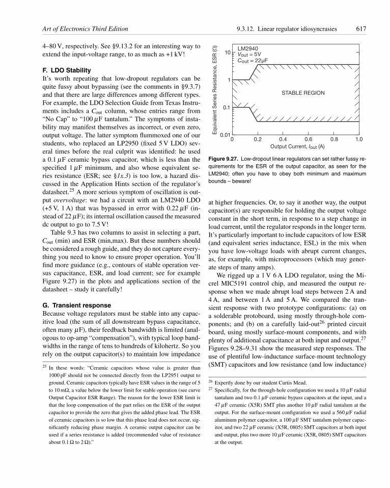
Art of Electronics Third Edition 9.3.12. Linear regulator idiosyncrasies 617
4–80 V, respectively. See §9.13.2 for an interesting way toextend the input-voltage range, to as much as +1 kV!
F. LDO StabilityIt’s worth repeating that low-dropout regulators can bequite fussy about bypassing (see the comments in §9.3.7)and that there are large differences among different types.For example, the LDO Selection Guide from Texas Instru-ments includes a Cout column, whose entries range from“No Cap” to “100 μF tantalum.” The symptoms of insta-bility may manifest themselves as incorrect, or even zero,output voltage. The latter symptom flummoxed one of ourstudents, who replaced an LP2950 (fixed 5 V LDO) sev-eral times before the real culprit was identified: he useda 0.1 μF ceramic bypass capacitor, which is less than thespecified 1 μF minimum, and also whose equivalent se-ries resistance (ESR; see §1x.3) is too low, a hazard dis-cussed in the Application Hints section of the regulator’sdatasheet.25 A more serious symptom of oscillation is out-put overvoltage: we had a circuit with an LM2940 LDO(+5 V, 1 A) that was bypassed in error with 0.22 μF (in-stead of 22 μF); its internal oscillation caused the measureddc output to go to 7.5 V!
Table 9.3 has two columns to assist in selecting a part,Cout (min) and ESR (min,max). But these numbers shouldbe considered a rough guide, and they do not capture every-thing you need to know to ensure proper operation. You’llfind more guidance (e.g., contours of stable operation ver-sus capacitance, ESR, and load current; see for exampleFigure 9.27) in the plots and applications section of thedatasheet – study it carefully!
G. Transient responseBecause voltage regulators must be stable into any capac-itive load (the sum of all downstream bypass capacitance,often many μF), their feedback bandwidth is limited (anal-ogous to op-amp “compensation”), with typical loop band-widths in the range of tens to hundreds of kilohertz. So yourely on the output capacitor(s) to maintain low impedance
25 In these words: “Ceramic capacitors whose value is greater than1000 pF should not be connected directly from the LP2951 output toground. Ceramic capacitors typically have ESR values in the range of 5to 10 mΩ, a value below the lower limit for stable operation (see curveOutput Capacitor ESR Range). The reason for the lower ESR limit isthat the loop compensation of the part relies on the ESR of the outputcapacitor to provide the zero that gives the added phase lead. The ESRof ceramic capacitors is so low that this phase lead does not occur, sig-nificantly reducing phase margin. A ceramic output capacitor can beused if a series resistance is added (recommended value of resistanceabout 0.1 Ω to 2 Ω).”
0.01
0.1
1
10
1.00.6 0.80.40.2
Cout = 22μFVout = 5V
STABLE REGION
LM2940
0Output Current, Iout (A)
Equ
ival
ent S
erie
s R
esis
tanc
e, E
SR
(Ω)
Figure 9.27. Low-dropout linear regulators can set rather fussy re-quirements for the ESR of the output capacitor, as seen for theLM2940; often you have to obey both minimum and maximumbounds – beware!
at higher frequencies. Or, to say it another way, the outputcapacitor(s) are responsible for holding the output voltageconstant in the short term, in response to a step change inload current, until the regulator responds in the longer term.It’s particularly important to include capacitors of low ESR(and equivalent series inductance, ESL) in the mix whenyou have low-voltage loads with abrupt current changes,as, for example, with microprocessors (which may gener-ate steps of many amps).
We rigged up a 1 V 6 A LDO regulator, using the Mi-crel MIC5191 control chip, and measured the output re-sponse when we made abrupt load steps between 2 A and4 A, and between 1 A and 5 A. We compared the tran-sient response with two prototype configurations: (a) ona solderable protoboard, using mostly through-hole com-ponents; and (b) on a carefully laid-out26 printed circuitboard, using mostly surface-mount components, and withplenty of additional capacitance at both input and output.27
Figures 9.28–9.31 show the measured step responses. Theuse of plentiful low-inductance surface-mount technology(SMT) capacitors and low resistance (and low inductance)
26 Expertly done by our student Curtis Mead.27 Specifically, for the through-hole configuration we used a 10 μF radial
tantalum and two 0.1 μF ceramic bypass capacitors at the input, and a47 μF ceramic (X5R) SMT plus another 10 μF radial tantalum at theoutput. For the surface-mount configuration we used a 560 μF radialaluminum polymer capacitor, a 100 μF SMT tantalum polymer capac-itor, and two 22 μF ceramic (X5R, 0805) SMT capacitors at both inputand output, plus two more 10 μF ceramic (X5R, 0805) SMT capacitorsat the output.
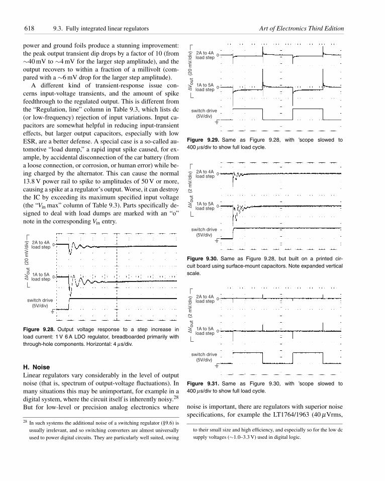
618 9.3. Fully integrated linear regulators Art of Electronics Third Edition
power and ground foils produce a stunning improvement:the peak output transient dip drops by a factor of 10 (from∼40 mV to ∼4 mV for the larger step amplitude), and theoutput recovers to within a fraction of a millivolt (com-pared with a ∼6 mV drop for the larger step amplitude).
A different kind of transient-response issue con-cerns input-voltage transients, and the amount of spikefeedthrough to the regulated output. This is different fromthe “Regulation, line” column in Table 9.3, which lists dc(or low-frequency) rejection of input variations. Input ca-pacitors are somewhat helpful in reducing input-transienteffects, but larger output capacitors, especially with lowESR, are a better defense. A special case is a so-called au-tomotive “load dump,” a rapid input spike caused, for ex-ample, by accidental disconnection of the car battery (froma loose connection, or corrosion, or human error) while be-ing charged by the alternator. This can cause the normal13.8 V power rail to spike to amplitudes of 50 V or more,causing a spike at a regulator’s output. Worse, it can destroythe IC by exceeding its maximum specified input voltage(the “Vin max” column of Table 9.3). Parts specifically de-signed to deal with load dumps are marked with an “o”note in the corresponding Vin entry.
2A to 4Aload step
1A to 5Aload step
0
0
switch drive(5V/div)
ΔV
out
(20
mV
/div
)
Figure 9.28. Output voltage response to a step increase inload current: 1 V 6 A LDO regulator, breadboarded primarily withthrough-hole components. Horizontal: 4 μs/div.
H. NoiseLinear regulators vary considerably in the level of outputnoise (that is, spectrum of output-voltage fluctuations). Inmany situations this may be unimportant, for example in adigital system, where the circuit itself is inherently noisy.28
But for low-level or precision analog electronics where
28 In such systems the additional noise of a switching regulator (§9.6) isusually irrelevant, and so switching converters are almost universallyused to power digital circuits. They are particularly well suited, owing
2A to 4Aload step
1A to 5Aload step
0
0
switch drive(5V/div)
ΔV
out
(20
mV
/div
)
Figure 9.29. Same as Figure 9.28, with ’scope slowed to400 μs/div to show full load cycle.
2A to 4Aload step
1A to 5Aload step
0
0
switch drive(5V/div)
ΔV
out
(2
mV
/div
)
Figure 9.30. Same as Figure 9.28, but built on a printed cir-cuit board using surface-mount capacitors. Note expanded verticalscale.
2A to 4Aload step
1A to 5Aload step
0
0
switch drive(5V/div)
ΔV
out
(2
mV
/div
)
Figure 9.31. Same as Figure 9.30, with ’scope slowed to400 μs/div to show full load cycle.
noise is important, there are regulators with superior noisespecifications, for example the LT1764/1963 (40 μVrms,
to their small size and high efficiency, and especially so for the low dcsupply voltages (∼1.0–3.3 V) used in digital logic.
Art of Electronics Third Edition 9.3.13. Noise and ripple filtering 619
10 Hz–100 kHz) or the ADP7102/04 (15 μVrms). Addi-tionally, some regulators provide access to the internal volt-age reference, so that an external filter capacitor can beadded to suppress all but the low-frequency end of thenoise spectrum, for example the LT1964 negative regula-tor (30 μVrms with 10 nF capacitor); see §9.3.13.
Because manufacturers specify noise characteristics dif-ferently (bandwidth, rms versus peak-to-peak, etc.), it canbe difficult to compare candidate parts. We’ve made an at-tempt in the Vn@Vout columns of Table 9.3, but be sure toconsult the footnotes (and then the datasheets).
I. Shutdown protectionSome regulator types can be damaged if they see a large ca-pacitance at their output, and the input voltage is broughtabruptly to zero (e.g., by a crowbar, or an accidental short-circuit). In that situation the charged output capacitancecan source a destructive current back into the regulator’soutput terminal. Figure 9.32 shows how to prevent suchdamage, in this case with the popular LM317. Althoughmany engineers don’t bother with this nicety, it is the markof a careful circuit designer. A similar hazard exists whenan external bypass capacitor is used to filter the voltagenoise of the regulator’s reference; see §9.3.13.29
LM317
D1
1N4001
IN
Cin Cout
OUT
SET
+Vin +Vout
+ +Cload
+
Figure 9.32. Diode D1 protects the regulator if the input is sud-denly grounded.
9.3.13 Noise and ripple filtering
The output noise from a linear regulator is caused by noisein the reference, multiplied by the ratio of Vout/Vref, com-bined with noise in the error amplifier, and with noise and
29 Many LDO regulator ICs include an internal diode sufficiently hardyto handle the reverse-discharge energy in modest (e.g., ≤10 μF) loadcapacitors. These are marked with a triangle symbol (�) in the “reverseblock” column in Table 9.3. Other parts do not discharge the outputcapacitor if the input voltage is taken below the output; these ICs aremarked with either a bullet dot (•) or a square (�).
ripple at the input terminal that is not completely sup-pressed by feedback.30 Some regulators let you add an ex-ternal capacitor for lowpass filtering of the internal voltagereference and thus the dc output. Figure 9.33 shows severalexamples. In Figure 9.33A the ADJ pin of the LM317-style3-terminal adjustable regulator is bypassed to ground; thisprovides significant noise improvement by preventing mul-tiplication of the reference noise voltage by the factor 1 +R2/R1 (the ratio of output voltage to 1.25 V reference volt-age). It also improves the input ripple rejection ratio, from65 dB to 80 dB (typical), according to the datasheet. Notethe additional protection diode D2, needed if the noise by-pass capacitor C1 is greater than 10 μF.
This scheme does not eliminate the reference noise, itjust prevents it (an ac signal) from being “gained up” by thedc gain factor Vout/Vref. The noise filtering in Figures 9.33Band C is more effective, because it filters the reference volt-age directly. In Figure 9.33B the LT3080’s SET pin, sourc-ing a stable 10 μA current, is converted to the output volt-age by RSET, filtered by C1; the regulator’s output is a unity-gain replica of this filtered voltage. With C1 = 0.1 μF, thereference noise is less than that of the error amplifier, pro-ducing an output noise of ∼40 μVrms (10 Hz–100 kHz).Note that the noise-filtering capacitor slows the regula-tor’s startup: a 0.1 μF capacitor in a 10 V regulator cir-cuit (RSET=1 MΩ) has a startup time constant RSETC1 of100 ms.
Finally, Figure 9.33C shows a CMOS low-dropout reg-ulator with a dedicated noise-reduction (NR) pin, for filter-ing directly the reference voltage presented to the error am-plifier. With the recommended 0.1 μF capacitor the outputnoise voltage is ∼40 μVrms (100 Hz–100 kHz). Regulatorswith this feature are marked in the “Filter pin” column ofTable 9.3.
Prefiltering An effective way of reducing dramaticallythe output ripple at the powerline frequency (and its har-monics) is to prefilter the dc input to the regulator. Thisis also highly effective in attenuating broadband noise thatmay be present at the dc input; and it’s easier than the al-ternative of increasing the regulator loop’s gain and band-width. We discuss this in some detail in §8.15.1 (“Capac-itance multiplier”), where we show the measured effectsof prefiltering versus the brute-force approach of piling onlots of output capacitance (Figure 8.122).
See further discussion of noise in §9.10, in connectionwith voltage references.
30 Table 9.3 includes a “Line regulation” column, but note that this is atdc and low frequencies where the loop gain is high; it is not necessarilyindicative of high-frequency supply-noise rejection.
620 9.3. Fully integrated linear regulators Art of Electronics Third Edition
LM317
1.25V
ADJ
Cin
+Vin +Vout
+Cout
+
+
+1
D1
D2R1
C1
10μF
C1
0.1μF
R2
A.
Cin
Vref
1.23V
+Vout
+
Cout
+
+
+
–
250k
NR
TPS796xx
LT3080
10.0μA
SET
Cin
+Vin
+Vin
+
+Vout
Cout
+
+1
RSET
B.
C.
0.1μF
Figure 9.33. Reducing output-voltage noise (and improving tran-sient line regulation) in linear regulators.
9.3.14 Current sources
A. Three-terminal regulators as current sourcesA 3-terminal linear regulator can be used to make a sim-ple current source by putting a resistor across the regu-lated output voltage (hence constant current IR = Vreg/R),and floating the whole thing on top of a load returnedto ground (Figure 9.34A). The current source is imper-fect, however, because the regulator’s operating current Ireg
(which comes out the ground pin) is combined with thewell-controlled resistor current to produce a total output
current Iout =Vreg/R + Ireg. It’s a reasonable current source,though, for output currents much larger than the regulator’soperating current.
Originally this circuit had been implemented with a7805, which has an operating current of ∼3 mA and addi-tionally has the disadvantage of squandering a rather large5 V (the lowest-voltage part in the 78xx series) to define the
7805, etc
IN
R
OUT
GND
1μF
~50μA
+Vin
+
LT3080
LT3092
Rset 100k
IN
VC
R1
OUT
SET
CCOMP
+
LOAD
A.
Ireg
IR = Vreg/R
Vreg = 5V
LT3080
IN OUT
curr adj1mA to 1A
100k
SET1μF
1Ω
10μA
+Vin
VC+
4.7μF+
LOAD
C.
D.
Iout
1mA to 1A
LM317
IN
R
OUT
ADJ
B.
I = 1.25V/R5mA to 1.5A
I = 1V/R1
1mA to 1A
Figure 9.34. Three-terminal regulators used as current sources.The bypass and compensation capacitors can be eliminated in cir-cuits C and D if the LT3080 is replaced by its internally compen-sated LT3092 variant (whose output current is limited to a maxi-mum of 200 mA).
Art of Electronics Third Edition 9.3.14. Current sources 621
output current. Happily, with regulators like the LM317,this circuit (Figure 9.34B) becomes more attractive: only1.25 V is used to set the current; and the regulator’s op-erating current (∼5 mA) emerges from the output pin, andthus is accurately accounted for in setting Iout =Vref/R. Theonly error term is the ADJ pin current of ∼50 μA, whichgets added to the current through R: Iout = Vref/R + IADJ.Because the minimum output current of 5 mA is 100 timeslarger, that is a small error even at the minimum outputcurrent, and smaller still at currents up to the regulator’smaximum of 1.5 A. For this circuit, then, the output-currentrange is 5 mA–1.5 A. It requires a minimum voltage dropof 1.25 V plus the regulator’s dropout voltage, or about 3 V;the maximum voltage across the two terminals is limitedeither to 40 V or (at higher currents) to the maximum junc-tion temperature of 125◦C (as determined by power dissi-pation and heatsinking), whichever is less.31
With the admirable LT3080-style regulator you can dobetter still, because its 10 μA SET-pin current reference letsyou set the voltage across the current-setting resistor to bemuch less than the 1.25 V of a 317-style voltage-referenceregulator. Its operating current is smaller as well (<1 mA),and the SET pin current (which gets added to the outputcurrent) is a stable and accurate 10.0 μA. Figure 9.34Cshows how to make a (1-terminal) current source to groundwith an LT3080, and Figure 9.34D shows how to make a 2-terminal “floating” current source, analogous to the LM317current-source circuit. As with the latter, the voltage dropis limited to a maximum of 40 V (less at higher currents)at the high end; its lower dropout and low SET-derivedreference voltage allows operation down to ∼1.5 V drop.The LT3092-series is a nice variant of the LT3080, de-signed specifically for use as a 2-terminal current source. Ituses the same 10 μA reference current, and operates from1.2 V to 40 V drop; its internal compensation is configuredto require no external bypass or compensation capacitors.Based on the LT3092’s datasheet plot of output impedance,the device’s effective parallel capacitance is approximately100 pF at 1 mA, 800 pF at 10 mA, and 6 nF at 100 mA.
Figure 9.35 shows, on a greatly expanded scale, themeasured output currents of an LT3092 and an LM317,configured as 10 mA current sources. In our measurementsthe latter does a better job of maintaining constant cur-
31 While we haven’t experienced this ourselves, we’ve been told of pos-sible issues with LM317-based current sources, such as long turn-ontimes, voltage retention, and poor voltage-compliance above a fewkilohertz. It’s always wise to test circuit performance fully (especially,uh, creative circuits).
rent (versus voltage across it), but the LT3092 kicks in at alower voltage.
Note that the current sources in Figures 9.34B and Dare 2-terminal devices. Thus the load can be connected oneither side. For example, you could use such a circuit tosink current from a load returned to ground, by connectingthe load between ground and the input, and connecting the“output” to a negative voltage (of course, you could alwaysuse the negative-polarity 337, in a configuration analogousto Figure 9.34A.).
10.100
10.095
10.090
10.085
10.080C
urr
en
t (m
A)
403020100
Voltage (volts)
LT3092
LM317
Figure 9.35. Measured current versus voltage drop for the cur-rent sources of Figures 9.34B and D, configured as 10 mA 2-terminal current sources. For the LM317, R1=124 Ω; for the LT3092,R1=20 Ω and RSET=20k.
B. Lower currentsThe above regulator-derived current sources are best suitedfor substantial output currents. For lower currents, or forhigher voltages, there are some good alternatives.
LM334It’s worth knowing about the LM334 (originated by Na-tional Semiconductor), optimized for use as a low-power 2-terminal current source (Figure 9.36A). It comes in small-outline IC (SOIC) and TO-92 (transistor) packages andcosts about $1 in small quantities. You can use it all the waydown to 1 μA because the ADJ current is a small fractionof the total current; and it operates over a voltage range of1–40 V. It has one peculiarity, however: the output currentis temperature dependent – in fact, precisely proportionalto absolute temperature (PTAT). So although it is not theworld’s most stable current source, you can use it as a tem-perature sensor! At room temperature (20◦C, ∼293K) itstempco is about +0.34%/◦C.32
32 See also the discussion in §2x.3.
622 9.3. Fully integrated linear regulators Art of Electronics Third Edition
LM334
1:1
REF
200
100μA each
(2.5 to 40V)
A.
RSET
SST505
1mA (1 to 50V)
C.
B.
I ≈ 68mV/RSET (@25°C)
(1 to 40V)
LND150
200Ω
1mA (1 to 500V)
D.
IXCP10M90
300Ω
10mA (4 to 900V)
E.
Figure 9.36. 2-terminal current source alternatives.
REF200The REF200 is another current-source IC worth know-ing about (Figure 9.36B). It has a pair of floating high-quality 100 μA (±0.5%) 2-terminal current sources (out-put impedance >200 MΩ over a voltage range of 3.5 V–30 V). It comes in dual in-line packages (DIP) and SOICpackages and costs about $4 in small quantities. Unlikethe LM334, the REF200’s current sources are tempera-ture stable (±25ppm/◦C, typ). It also has an on-chip unit-ratio current mirror, so you can make a 2-terminal cur-rent source with fixed currents of 50 μA, 100 μA, 200 μA,300 μA, or 400 μA. The datasheet asserts that “applica-tions for the REF200 are limitless,” though we are skep-tical. Figure 9.37 shows measured current versus voltagefor the parallel connection of the 100 μA pair.
Discrete-component current sourcesWhen thinking about current sources, don’t forget about2-terminal devices like
(a) the humble JFET “current-regulator diode” (§3.2.2),which makes a simple 2-terminal current source (Fig-ure 9.36C) that operates nicely up to 100 V (we plottedmeasured current versus voltage in Figure 9.38);
(b) a discrete JFET (see Tables 3.1, 3.7, and 8.2), config-ured similarly as a 2-terminal current source;
(c) the analogous use of a depletion-mode MOSFET (seeTable 3.6 on page 210) like the Supertex LND150 (Fig-ure 9.36D), discussed on this page (§9.3.14C);
(d) the series of 2-terminal “Constant Current Regu-
201
200
199
Cur
rent
(μA
)
403020100Voltage (volts)
Figure 9.37. Measured current versus voltage for the REF200 two-terminal current source (parallel connection of the 100 μA pair).
lator and LED Driver” devices from ON Semi-conductor. These are inexpensive ($0.10–$0.20 inqty 100), and are offered with selected currents(e.g., NSI50010YT1G: 10 mA, 50 V; NSIC2020BT3G:20 mA, 120 V) and in adjustable versions (e.g.,NSI45020JZ: 20–40 mA, 45 V). The datasheets don’tsay much about what’s inside these things, butdepletion-mode FETs are the likely culprits.
Op-amp current-source configurationsIf the application does not require a floating current source,then consider also
(d) the simple BJT current source (§2.2.6), drawn schemat-ically in Figure 9.39A;
(e) the op-amp assisted BJT current source (§4.2.5), Fig-ure 9.39B;
(f) the Howland current source (§4.2.5B), Figure 9.39C.
In these last three figures the bias voltage that programsthe current is drawn as a floating battery; in a circuit imple-mentation it would be a voltage relative to ground or to asupply rail, derived from a voltage reference.
C. High-voltage discrete current sourceAs mentioned above in the paragraph on discrete-component current sources, a simple source-biaseddepletion-mode MOSFET (Figures 9.36D and E) formsa pretty good 2-terminal current source. These partscome in convenient packages (TO-92, SMT, TO-220,D2PAK), with voltage ratings to 1.7 kV; familiar exam-ples are the LND150 and DN3545 from Supertex and theIXCP10M45S and IXCP10M90S from IXYS – see Ta-ble 3.6 on page 210. Because of the uncertainty in ID versusVGS, this sort of current source is not particularly precise or
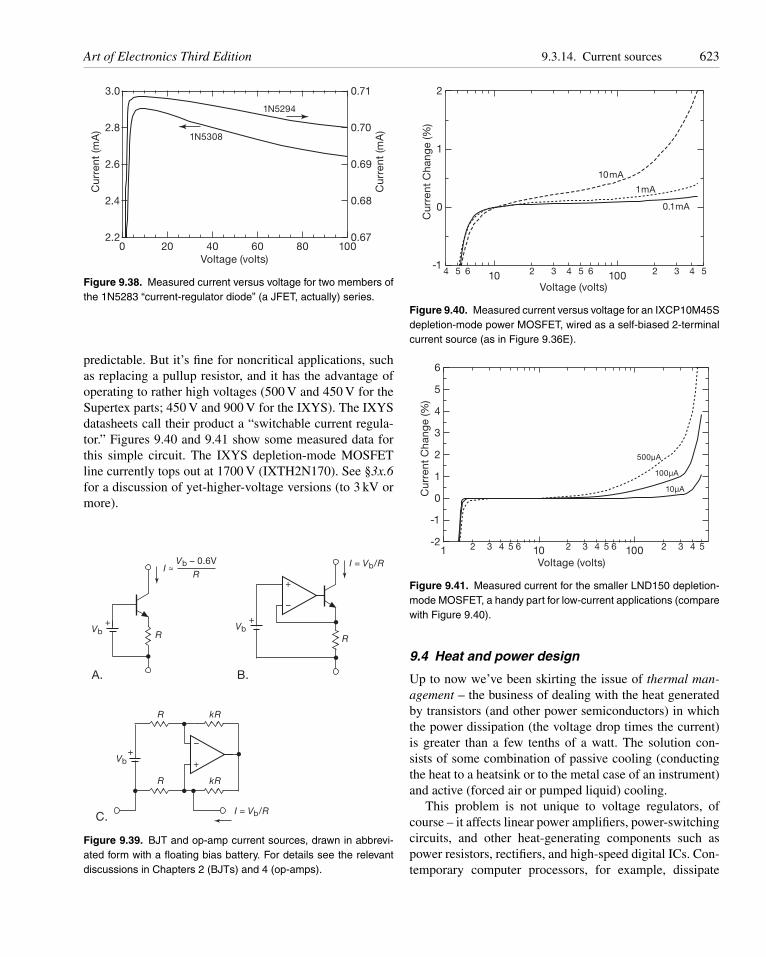
Art of Electronics Third Edition 9.3.14. Current sources 623
3.0
2.8
2.6
2.4
2.2
Cur
rent
(mA
)
Cur
rent
(mA
)
100806040200Voltage (volts)
0.71
0.70
0.69
0.68
0.67
1N5294
1N5308
Figure 9.38. Measured current versus voltage for two members ofthe 1N5283 “current-regulator diode” (a JFET, actually) series.
predictable. But it’s fine for noncritical applications, suchas replacing a pullup resistor, and it has the advantage ofoperating to rather high voltages (500 V and 450 V for theSupertex parts; 450 V and 900 V for the IXYS). The IXYSdatasheets call their product a “switchable current regula-tor.” Figures 9.40 and 9.41 show some measured data forthis simple circuit. The IXYS depletion-mode MOSFETline currently tops out at 1700 V (IXTH2N170). See §3x.6for a discussion of yet-higher-voltage versions (to 3 kV ormore).
I = Vb/RVb – 0.6V
RI ≈
R R
R kR
R kR
Vb+ Vb
+
A. B.
Vb+
C.I = Vb/R
+
–
+
–
Figure 9.39. BJT and op-amp current sources, drawn in abbrevi-ated form with a floating bias battery. For details see the relevantdiscussions in Chapters 2 (BJTs) and 4 (op-amps).
2
1
0
-1
Cur
rent
Cha
nge
(%)
4 5 6 10 2 3 4 5 6 100 2 3 4 5
Voltage (volts)
0.1mA
1mA
10mA
Figure 9.40. Measured current versus voltage for an IXCP10M45Sdepletion-mode power MOSFET, wired as a self-biased 2-terminalcurrent source (as in Figure 9.36E).
6
5
4
3
2
1
0
-1
-2
Cur
rent
Cha
nge
(%)
1 2 3 4 5 6 10 2 3 4 5 6 100 2 3 4 5
Voltage (volts)
500μA
100μA
10μA
Figure 9.41. Measured current for the smaller LND150 depletion-mode MOSFET, a handy part for low-current applications (comparewith Figure 9.40).
9.4 Heat and power design
Up to now we’ve been skirting the issue of thermal man-agement – the business of dealing with the heat generatedby transistors (and other power semiconductors) in whichthe power dissipation (the voltage drop times the current)is greater than a few tenths of a watt. The solution con-sists of some combination of passive cooling (conductingthe heat to a heatsink or to the metal case of an instrument)and active (forced air or pumped liquid) cooling.
This problem is not unique to voltage regulators, ofcourse – it affects linear power amplifiers, power-switchingcircuits, and other heat-generating components such aspower resistors, rectifiers, and high-speed digital ICs. Con-temporary computer processors, for example, dissipate
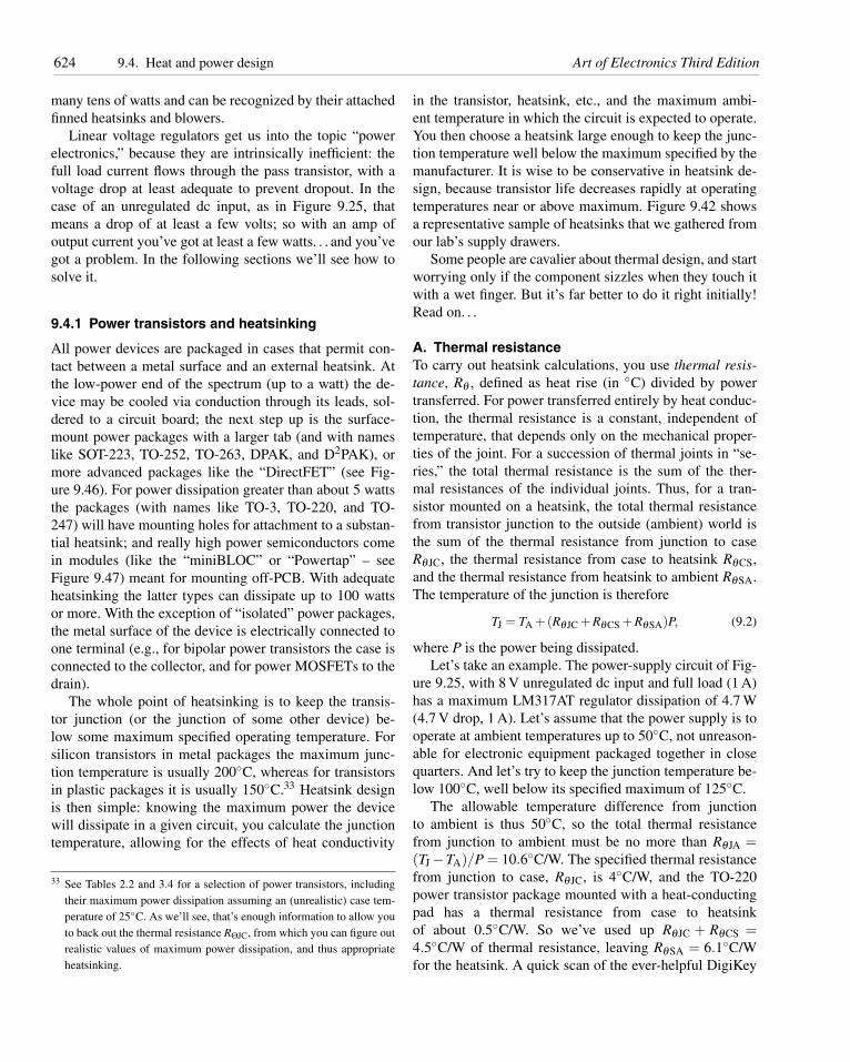
624 9.4. Heat and power design Art of Electronics Third Edition
many tens of watts and can be recognized by their attachedfinned heatsinks and blowers.
Linear voltage regulators get us into the topic “powerelectronics,” because they are intrinsically inefficient: thefull load current flows through the pass transistor, with avoltage drop at least adequate to prevent dropout. In thecase of an unregulated dc input, as in Figure 9.25, thatmeans a drop of at least a few volts; so with an amp ofoutput current you’ve got at least a few watts. . . and you’vegot a problem. In the following sections we’ll see how tosolve it.
9.4.1 Power transistors and heatsinking
All power devices are packaged in cases that permit con-tact between a metal surface and an external heatsink. Atthe low-power end of the spectrum (up to a watt) the de-vice may be cooled via conduction through its leads, sol-dered to a circuit board; the next step up is the surface-mount power packages with a larger tab (and with nameslike SOT-223, TO-252, TO-263, DPAK, and D2PAK), ormore advanced packages like the “DirectFET” (see Fig-ure 9.46). For power dissipation greater than about 5 wattsthe packages (with names like TO-3, TO-220, and TO-247) will have mounting holes for attachment to a substan-tial heatsink; and really high power semiconductors comein modules (like the “miniBLOC” or “Powertap” – seeFigure 9.47) meant for mounting off-PCB. With adequateheatsinking the latter types can dissipate up to 100 wattsor more. With the exception of “isolated” power packages,the metal surface of the device is electrically connected toone terminal (e.g., for bipolar power transistors the case isconnected to the collector, and for power MOSFETs to thedrain).
The whole point of heatsinking is to keep the transis-tor junction (or the junction of some other device) be-low some maximum specified operating temperature. Forsilicon transistors in metal packages the maximum junc-tion temperature is usually 200◦C, whereas for transistorsin plastic packages it is usually 150◦C.33 Heatsink designis then simple: knowing the maximum power the devicewill dissipate in a given circuit, you calculate the junctiontemperature, allowing for the effects of heat conductivity
33 See Tables 2.2 and 3.4 for a selection of power transistors, includingtheir maximum power dissipation assuming an (unrealistic) case tem-perature of 25◦C. As we’ll see, that’s enough information to allow youto back out the thermal resistance RΘJC, from which you can figure outrealistic values of maximum power dissipation, and thus appropriateheatsinking.
in the transistor, heatsink, etc., and the maximum ambi-ent temperature in which the circuit is expected to operate.You then choose a heatsink large enough to keep the junc-tion temperature well below the maximum specified by themanufacturer. It is wise to be conservative in heatsink de-sign, because transistor life decreases rapidly at operatingtemperatures near or above maximum. Figure 9.42 showsa representative sample of heatsinks that we gathered fromour lab’s supply drawers.
Some people are cavalier about thermal design, and startworrying only if the component sizzles when they touch itwith a wet finger. But it’s far better to do it right initially!Read on. . .
A. Thermal resistanceTo carry out heatsink calculations, you use thermal resis-tance, Rθ , defined as heat rise (in ◦C) divided by powertransferred. For power transferred entirely by heat conduc-tion, the thermal resistance is a constant, independent oftemperature, that depends only on the mechanical proper-ties of the joint. For a succession of thermal joints in “se-ries,” the total thermal resistance is the sum of the ther-mal resistances of the individual joints. Thus, for a tran-sistor mounted on a heatsink, the total thermal resistancefrom transistor junction to the outside (ambient) world isthe sum of the thermal resistance from junction to caseRθJC, the thermal resistance from case to heatsink RθCS,and the thermal resistance from heatsink to ambient RθSA.The temperature of the junction is therefore
TJ = TA +(RθJC +RθCS +RθSA)P, (9.2)
where P is the power being dissipated.Let’s take an example. The power-supply circuit of Fig-
ure 9.25, with 8 V unregulated dc input and full load (1 A)has a maximum LM317AT regulator dissipation of 4.7 W(4.7 V drop, 1 A). Let’s assume that the power supply is tooperate at ambient temperatures up to 50◦C, not unreason-able for electronic equipment packaged together in closequarters. And let’s try to keep the junction temperature be-low 100◦C, well below its specified maximum of 125◦C.
The allowable temperature difference from junctionto ambient is thus 50◦C, so the total thermal resistancefrom junction to ambient must be no more than RθJA =(TJ −TA)/P = 10.6◦C/W. The specified thermal resistancefrom junction to case, RθJC, is 4◦C/W, and the TO-220power transistor package mounted with a heat-conductingpad has a thermal resistance from case to heatsinkof about 0.5◦C/W. So we’ve used up RθJC + RθCS =4.5◦C/W of thermal resistance, leaving RθSA = 6.1◦C/Wfor the heatsink. A quick scan of the ever-helpful DigiKey
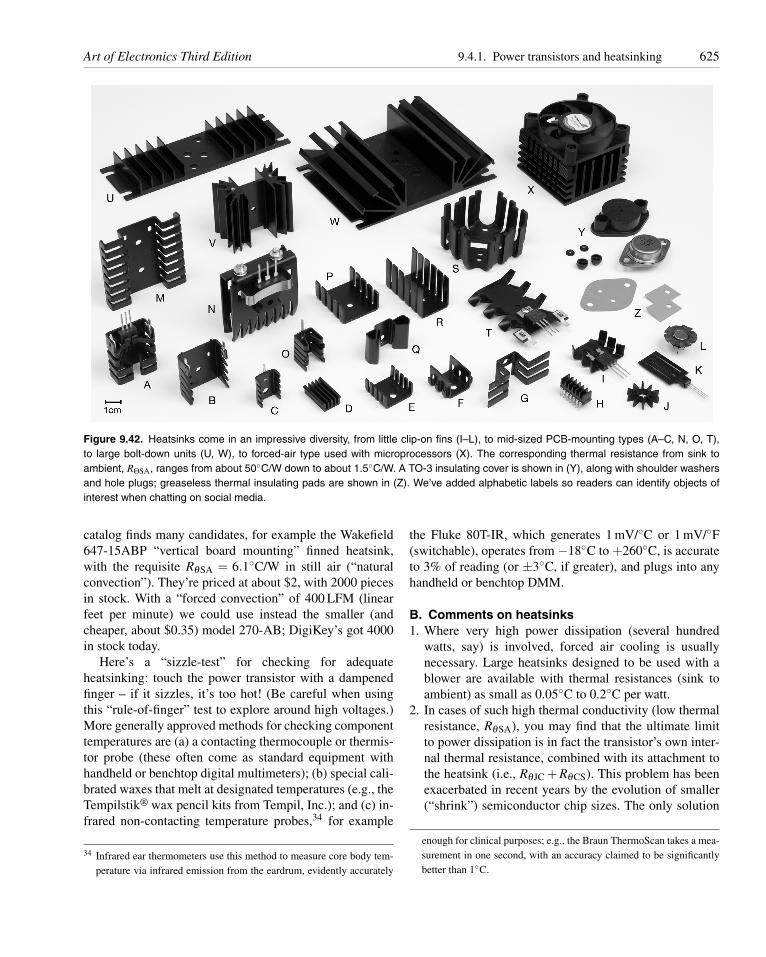
Art of Electronics Third Edition 9.4.1. Power transistors and heatsinking 625
Figure 9.42. Heatsinks come in an impressive diversity, from little clip-on fins (I–L), to mid-sized PCB-mounting types (A–C, N, O, T),to large bolt-down units (U, W), to forced-air type used with microprocessors (X). The corresponding thermal resistance from sink toambient, RΘSA, ranges from about 50◦C/W down to about 1.5◦C/W. A TO-3 insulating cover is shown in (Y), along with shoulder washersand hole plugs; greaseless thermal insulating pads are shown in (Z). We’ve added alphabetic labels so readers can identify objects ofinterest when chatting on social media.
catalog finds many candidates, for example the Wakefield647-15ABP “vertical board mounting” finned heatsink,with the requisite RθSA = 6.1◦C/W in still air (“naturalconvection”). They’re priced at about $2, with 2000 piecesin stock. With a “forced convection” of 400 LFM (linearfeet per minute) we could use instead the smaller (andcheaper, about $0.35) model 270-AB; DigiKey’s got 4000in stock today.
Here’s a “sizzle-test” for checking for adequateheatsinking: touch the power transistor with a dampenedfinger – if it sizzles, it’s too hot! (Be careful when usingthis “rule-of-finger” test to explore around high voltages.)More generally approved methods for checking componenttemperatures are (a) a contacting thermocouple or thermis-tor probe (these often come as standard equipment withhandheld or benchtop digital multimeters); (b) special cali-brated waxes that melt at designated temperatures (e.g., theTempilstik® wax pencil kits from Tempil, Inc.); and (c) in-frared non-contacting temperature probes,34 for example
34 Infrared ear thermometers use this method to measure core body tem-perature via infrared emission from the eardrum, evidently accurately
the Fluke 80T-IR, which generates 1 mV/◦C or 1 mV/◦F(switchable), operates from −18◦C to +260◦C, is accurateto 3% of reading (or ±3◦C, if greater), and plugs into anyhandheld or benchtop DMM.
B. Comments on heatsinks1. Where very high power dissipation (several hundred
watts, say) is involved, forced air cooling is usuallynecessary. Large heatsinks designed to be used with ablower are available with thermal resistances (sink toambient) as small as 0.05◦C to 0.2◦C per watt.
2. In cases of such high thermal conductivity (low thermalresistance, RθSA), you may find that the ultimate limitto power dissipation is in fact the transistor’s own inter-nal thermal resistance, combined with its attachment tothe heatsink (i.e., RθJC + RθCS). This problem has beenexacerbated in recent years by the evolution of smaller(“shrink”) semiconductor chip sizes. The only solution
enough for clinical purposes; e.g., the Braun ThermoScan takes a mea-surement in one second, with an accuracy claimed to be significantlybetter than 1◦C.
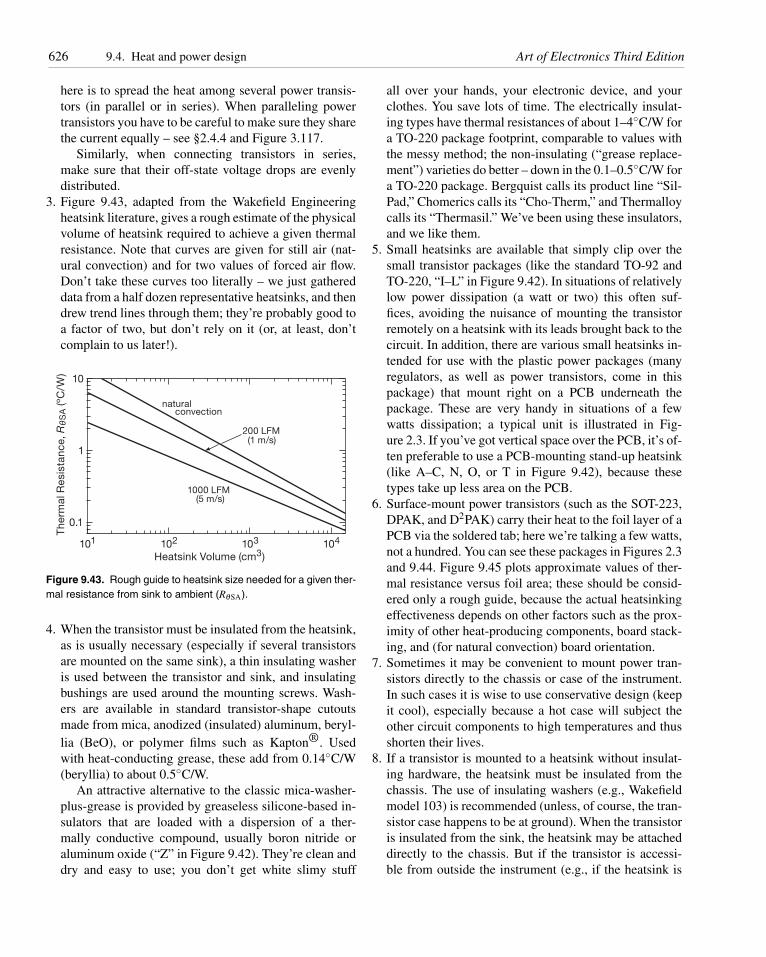
626 9.4. Heat and power design Art of Electronics Third Edition
here is to spread the heat among several power transis-tors (in parallel or in series). When paralleling powertransistors you have to be careful to make sure they sharethe current equally – see §2.4.4 and Figure 3.117.
Similarly, when connecting transistors in series,make sure that their off-state voltage drops are evenlydistributed.
3. Figure 9.43, adapted from the Wakefield Engineeringheatsink literature, gives a rough estimate of the physicalvolume of heatsink required to achieve a given thermalresistance. Note that curves are given for still air (nat-ural convection) and for two values of forced air flow.Don’t take these curves too literally – we just gathereddata from a half dozen representative heatsinks, and thendrew trend lines through them; they’re probably good toa factor of two, but don’t rely on it (or, at least, don’tcomplain to us later!).
0.1
1
10
The
rmal
Res
ista
nce,
Rθ
SA (º
C/W
)
101 102 103 104
Heatsink Volume (cm3)
natural
1000 LFM(5 m/s)
(1 m/s)200 LFM
convection
Figure 9.43. Rough guide to heatsink size needed for a given ther-mal resistance from sink to ambient (RθSA).
4. When the transistor must be insulated from the heatsink,as is usually necessary (especially if several transistorsare mounted on the same sink), a thin insulating washeris used between the transistor and sink, and insulatingbushings are used around the mounting screws. Wash-ers are available in standard transistor-shape cutoutsmade from mica, anodized (insulated) aluminum, beryl-lia (BeO), or polymer films such as Kapton®. Usedwith heat-conducting grease, these add from 0.14◦C/W(beryllia) to about 0.5◦C/W.
An attractive alternative to the classic mica-washer-plus-grease is provided by greaseless silicone-based in-sulators that are loaded with a dispersion of a ther-mally conductive compound, usually boron nitride oraluminum oxide (“Z” in Figure 9.42). They’re clean anddry and easy to use; you don’t get white slimy stuff
all over your hands, your electronic device, and yourclothes. You save lots of time. The electrically insulat-ing types have thermal resistances of about 1–4◦C/W fora TO-220 package footprint, comparable to values withthe messy method; the non-insulating (“grease replace-ment”) varieties do better – down in the 0.1–0.5◦C/W fora TO-220 package. Bergquist calls its product line “Sil-Pad,” Chomerics calls its “Cho-Therm,” and Thermalloycalls its “Thermasil.” We’ve been using these insulators,and we like them.
5. Small heatsinks are available that simply clip over thesmall transistor packages (like the standard TO-92 andTO-220, “I–L” in Figure 9.42). In situations of relativelylow power dissipation (a watt or two) this often suf-fices, avoiding the nuisance of mounting the transistorremotely on a heatsink with its leads brought back to thecircuit. In addition, there are various small heatsinks in-tended for use with the plastic power packages (manyregulators, as well as power transistors, come in thispackage) that mount right on a PCB underneath thepackage. These are very handy in situations of a fewwatts dissipation; a typical unit is illustrated in Fig-ure 2.3. If you’ve got vertical space over the PCB, it’s of-ten preferable to use a PCB-mounting stand-up heatsink(like A–C, N, O, or T in Figure 9.42), because thesetypes take up less area on the PCB.
6. Surface-mount power transistors (such as the SOT-223,DPAK, and D2PAK) carry their heat to the foil layer of aPCB via the soldered tab; here we’re talking a few watts,not a hundred. You can see these packages in Figures 2.3and 9.44. Figure 9.45 plots approximate values of ther-mal resistance versus foil area; these should be consid-ered only a rough guide, because the actual heatsinkingeffectiveness depends on other factors such as the prox-imity of other heat-producing components, board stack-ing, and (for natural convection) board orientation.
7. Sometimes it may be convenient to mount power tran-sistors directly to the chassis or case of the instrument.In such cases it is wise to use conservative design (keepit cool), especially because a hot case will subject theother circuit components to high temperatures and thusshorten their lives.
8. If a transistor is mounted to a heatsink without insulat-ing hardware, the heatsink must be insulated from thechassis. The use of insulating washers (e.g., Wakefieldmodel 103) is recommended (unless, of course, the tran-sistor case happens to be at ground). When the transistoris insulated from the sink, the heatsink may be attacheddirectly to the chassis. But if the transistor is accessi-ble from outside the instrument (e.g., if the heatsink is
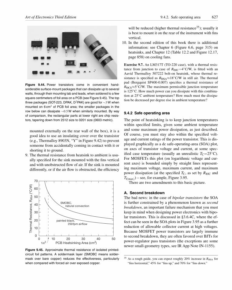
Art of Electronics Third Edition 9.4.2. Safe operating area 627
Figure 9.44. Power transistors come in convenient hand-solderable surface-mount packages that can dissipate up to severalwatts, through their mounting tab and leads, when soldered to a fewsquare centimeters of foil area on a PCB (see Figure 9.45). The topthree packages (SOT-223, DPAK, D2PAK) are good for ∼3 W whenmounted on 6 cm2 of PCB foil area; the smaller packages in therow below can dissipate ∼0.5 W when similarly mounted. By wayof comparison, the rectangular parts at lower right are chip resis-tors, tapering down from 2512 size to 0201 size (0603 metric).
mounted externally on the rear wall of the box), it is agood idea to use an insulating cover over the transistor(e.g., Thermalloy 8903N, “Y” in Figure 9.42) to preventsomeone from accidentally coming in contact with it orshorting it to ground.
9. The thermal resistance from heatsink to ambient is usu-ally specified for the sink mounted with the fins verticaland with unobstructed flow of air. If the sink is mounteddifferently, or if the air flow is obstructed, the efficiency
00
10
20
30
40
50
60
70
10 20 30 40 50PCB Heatsinking Area (cm2)
The
rmal
Res
ista
nce,
Rθ
SA (°
C/W
)
SMOBC,natural convection
painted black,250fpm airflow
1in2
Figure 9.45. Approximate thermal resistance of isolated printed-circuit foil patterns. A soldermask layer (SMOBC means solder-mask over bare copper) reduces the effectiveness, particularlywhen compared with forced air over exposed copper.
will be reduced (higher thermal resistance35); usually itis best to mount it on the rear of the instrument with finsvertical.
10. In the second edition of this book there is additionalinformation: see Chapter 6 (Figure 6.6, page 315) onheatsinks, and Chapter 12 (Table 12.2 and Figure 12.17,page 858) on cooling fans.
Exercise 9.7. An LM317T (TO-220 case), with a thermal resis-tance from junction to case of RΘJC=4◦C/W, is fitted with anAavid Thermalloy 507222 bolt-on heatsink, whose thermal re-sistance is specified as RΘSA≈18◦C/W in still air. The thermalpad (Bergquist SP400-0.007) specifies a thermal resistance ofRΘCS≈5◦C/W. The maximum permissible junction temperatureis 125◦C. How much power can you dissipate with this combina-tion at 25◦C ambient temperature? How much must the dissipa-tion be decreased per degree rise in ambient temperature?
9.4.2 Safe operating area
The point of heatsinking is to keep junction temperatureswithin specified limits, given some ambient temperatureand some maximum power dissipation, as just described.Of course, you must stay also within the specified volt-age and current ratings of the power transistor. This is dis-played graphically as a dc safe-operating-area (SOA) plot,on axes of transistor voltage and current, at some spec-ified case temperature (usually an unrealistic TC=25◦C).For MOSFETs this plot (on logarithmic voltage and cur-rent axes) is bounded simply by straight lines represent-ing maximum voltage, maximum current, and maximumpower dissipation (at the specified TC, as set by RθJC andTJ(max)) – see, for example, Figure 3.95.
There are two amendments to this basic picture.
A. Second breakdownThe bad news: in the case of bipolar transistors the SOAis further constrained by a phenomenon known as secondbreakdown, an important failure mechanism that you mustkeep in mind when designing power electronics with bipo-lar transistors. This is discussed in §3.6.4C, where the ef-fect can be seen in the SOA plots in Figure 3.95 as a furtherreduction of allowable collector current at high voltages.Because MOSFET power transistors are largely immuneto second breakdown, they are often favored over BJTs forpower-regulator pass transistors (the exceptions are somenewer small-geometry types, see IR App Note IN-1155).
35 As a rough guide, you can expect roughly 20% increase in RθSA for“fins horizontal,” 45% for “fins up,” and 70% for “fins down.”
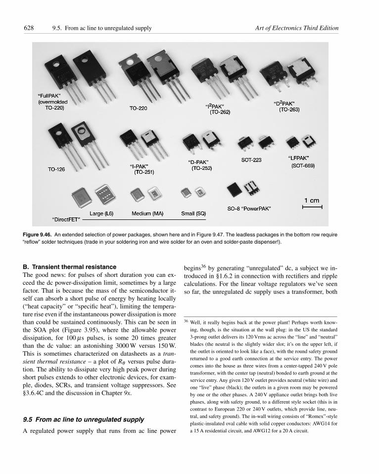
628 9.5. From ac line to unregulated supply Art of Electronics Third Edition
Figure 9.46. An extended selection of power packages, shown here and in Figure 9.47. The leadless packages in the bottom row require“reflow” solder techniques (trade in your soldering iron and wire solder for an oven and solder-paste dispenser!).
B. Transient thermal resistanceThe good news: for pulses of short duration you can ex-ceed the dc power-dissipation limit, sometimes by a largefactor. That is because the mass of the semiconductor it-self can absorb a short pulse of energy by heating locally(“heat capacity” or “specific heat”), limiting the tempera-ture rise even if the instantaneous power dissipation is morethan could be sustained continuously. This can be seen inthe SOA plot (Figure 3.95), where the allowable powerdissipation, for 100 μs pulses, is some 20 times greaterthan the dc value: an astonishing 3000 W versus 150 W.This is sometimes characterized on datasheets as a tran-sient thermal resistance – a plot of Rθ versus pulse dura-tion. The ability to dissipate very high peak power duringshort pulses extends to other electronic devices, for exam-ple, diodes, SCRs, and transient voltage suppressors. See§3.6.4C and the discussion in Chapter 9x.
9.5 From ac line to unregulated supply
A regulated power supply that runs from ac line power
begins36 by generating “unregulated” dc, a subject we in-troduced in §1.6.2 in connection with rectifiers and ripplecalculations. For the linear voltage regulators we’ve seenso far, the unregulated dc supply uses a transformer, both
36 Well, it really begins back at the power plant! Perhaps worth know-ing, though, is the situation at the wall plug: in the US the standard3-prong outlet delivers its 120 Vrms ac across the “line” and “neutral”blades (the neutral is the slightly wider slot; it’s on the upper left, ifthe outlet is oriented to look like a face), with the round safety groundreturned to a good earth connection at the service entry. The powercomes into the house as three wires from a center-tapped 240 V poletransformer, with the center tap (neutral) bonded to earth ground at theservice entry. Any given 120 V outlet provides neutral (white wire) andone “live” phase (black); the outlets in a given room may be poweredby one or the other phases. A 240 V appliance outlet brings both livephases, along with safety ground, to a different style socket (this is incontrast to European 220 or 240 V outlets, which provide line, neu-tral, and safety ground). The in-wall wiring consists of “Romex”-styleplastic-insulated oval cable with solid copper conductors: AWG14 fora 15 A residential circuit, and AWG12 for a 20 A circuit.
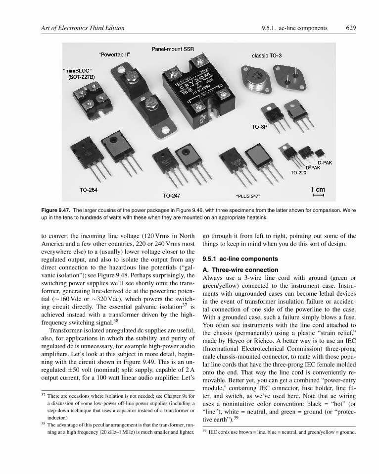
Art of Electronics Third Edition 9.5.1. ac-line components 629
Figure 9.47. The larger cousins of the power packages in Figure 9.46, with three specimens from the latter shown for comparison. We’reup in the tens to hundreds of watts with these when they are mounted on an appropriate heatsink.
to convert the incoming line voltage (120 Vrms in NorthAmerica and a few other countries, 220 or 240 Vrms mosteverywhere else) to a (usually) lower voltage closer to theregulated output, and also to isolate the output from anydirect connection to the hazardous line potentials (“gal-vanic isolation”); see Figure 9.48. Perhaps surprisingly, theswitching power supplies we’ll see shortly omit the trans-former, generating line-derived dc at the powerline poten-tial (∼160 Vdc or ∼320 Vdc), which powers the switch-ing circuit directly. The essential galvanic isolation37 isachieved instead with a transformer driven by the high-frequency switching signal.38
Transformer-isolated unregulated dc supplies are useful,also, for applications in which the stability and purity ofregulated dc is unnecessary, for example high-power audioamplifiers. Let’s look at this subject in more detail, begin-ning with the circuit shown in Figure 9.49. This is an un-regulated ±50 volt (nominal) split supply, capable of 2 Aoutput current, for a 100 watt linear audio amplifier. Let’s
37 There are occasions where isolation is not needed; see Chapter 9x fora discussion of some low-power off-line power supplies (including astep-down technique that uses a capacitor instead of a transformer orinductor.)
38 The advantage of this peculiar arrangement is that the transformer, run-ning at a high frequency (20 kHz–1 MHz) is much smaller and lighter.
go through it from left to right, pointing out some of thethings to keep in mind when you do this sort of design.
9.5.1 ac-line components
A. Three-wire connectionAlways use a 3-wire line cord with ground (green orgreen/yellow) connected to the instrument case. Instru-ments with ungrounded cases can become lethal devicesin the event of transformer insulation failure or acciden-tal connection of one side of the powerline to the case.With a grounded case, such a failure simply blows a fuse.You often see instruments with the line cord attached tothe chassis (permanently) using a plastic “strain relief,”made by Heyco or Richco. A better way is to use an IEC(International Electrotechnical Commission) three-prongmale chassis-mounted connector, to mate with those popu-lar line cords that have the three-prong IEC female moldedonto the end. That way the line cord is conveniently re-movable. Better yet, you can get a combined “power-entrymodule,” containing IEC connector, fuse holder, line fil-ter, and switch, as we’ve used here. Note that ac wiringuses a nonintuitive color convention: black = “hot” (or“line”), white = neutral, and green = ground (or “protec-tive earth”).39
39 IEC cords use brown = line, blue = neutral, and green/yellow = ground.
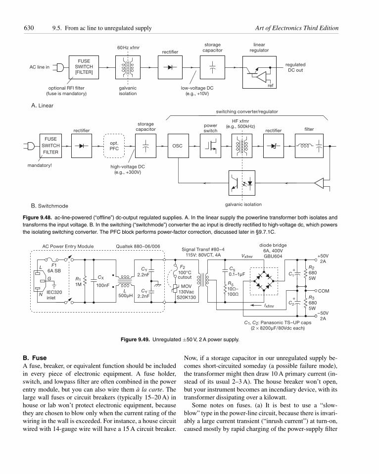
630 9.5. From ac line to unregulated supply Art of Electronics Third Edition
FUSE
SWITCH
[FILTER]
optional RFI filter
(fuse is mandatory)
A. Linear
galvanic
isolation
60Hz xfmrrectifier
storage
capacitor
linear
regulator
regulated
DC out
ref
AC line in
low-voltage DC
(e.g., +10V)
FUSE
SWITCH
FILTER
mandatory!
B. Switchmode
rectifier
galvanic isolation
HF xfmr(e.g., 500kHz)
rectifier filterstorage
capacitor
high-voltage DC
(e.g., +300V)
OSC
powerswitch
switching converter/regulator
opt.
PFC
Figure 9.48. ac-line-powered (“offline”) dc-output regulated supplies. A. In the linear supply the powerline transformer both isolates andtransforms the input voltage. B. In the switching (“switchmode”) converter the ac input is directly rectified to high-voltage dc, which powersthe isolating switching converter. The PFC block performs power-factor correction, discussed later in §9.7.1C.
AC Power Entry Module
L
LN
G
F1
6A SB
R1
1M
CX
CSC1
100°Ccutout
MOV
130Vac
S20K130
R2
680
5W
R3
680
5W
C2
RS
Vxfmr
Ixfmr
100nF
2.2nF
CY
CY
2.2nF500μH
0.1–1μF
10Ω–100Ω
Qualtek 880–06/006Signal Transf #80–4
115V: 80VCT, 4A
diode bridge
6A, 400V
GBU604 +50V
2A
–50V
2A
COM
C1, C2: Panasonic TS–UP caps
(2 × 8200μF/80Vdc each)
IEC320
inlet
F2+
+
Figure 9.49. Unregulated ±50 V, 2 A power supply.
B. FuseA fuse, breaker, or equivalent function should be includedin every piece of electronic equipment. A fuse holder,switch, and lowpass filter are often combined in the powerentry module, but you can also wire them a la carte. Thelarge wall fuses or circuit breakers (typically 15–20 A) inhouse or lab won’t protect electronic equipment, becausethey are chosen to blow only when the current rating of thewiring in the wall is exceeded. For instance, a house circuitwired with 14-gauge wire will have a 15 A circuit breaker.
Now, if a storage capacitor in our unregulated supply be-comes short-circuited someday (a possible failure mode),the transformer might then draw 10 A primary current (in-stead of its usual 2–3 A). The house breaker won’t open,but your instrument becomes an incendiary device, with itstransformer dissipating over a kilowatt.
Some notes on fuses. (a) It is best to use a “slow-blow” type in the power-line circuit, because there is invari-ably a large current transient (“inrush current”) at turn-on,caused mostly by rapid charging of the power-supply filter
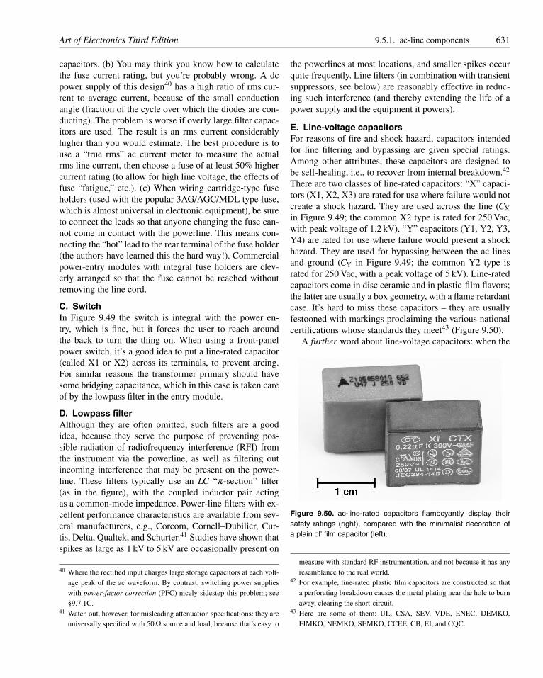
Art of Electronics Third Edition 9.5.1. ac-line components 631
capacitors. (b) You may think you know how to calculatethe fuse current rating, but you’re probably wrong. A dcpower supply of this design40 has a high ratio of rms cur-rent to average current, because of the small conductionangle (fraction of the cycle over which the diodes are con-ducting). The problem is worse if overly large filter capac-itors are used. The result is an rms current considerablyhigher than you would estimate. The best procedure is touse a “true rms” ac current meter to measure the actualrms line current, then choose a fuse of at least 50% highercurrent rating (to allow for high line voltage, the effects offuse “fatigue,” etc.). (c) When wiring cartridge-type fuseholders (used with the popular 3AG/AGC/MDL type fuse,which is almost universal in electronic equipment), be sureto connect the leads so that anyone changing the fuse can-not come in contact with the powerline. This means con-necting the “hot” lead to the rear terminal of the fuse holder(the authors have learned this the hard way!). Commercialpower-entry modules with integral fuse holders are clev-erly arranged so that the fuse cannot be reached withoutremoving the line cord.
C. SwitchIn Figure 9.49 the switch is integral with the power en-try, which is fine, but it forces the user to reach aroundthe back to turn the thing on. When using a front-panelpower switch, it’s a good idea to put a line-rated capacitor(called X1 or X2) across its terminals, to prevent arcing.For similar reasons the transformer primary should havesome bridging capacitance, which in this case is taken careof by the lowpass filter in the entry module.
D. Lowpass filterAlthough they are often omitted, such filters are a goodidea, because they serve the purpose of preventing pos-sible radiation of radiofrequency interference (RFI) fromthe instrument via the powerline, as well as filtering outincoming interference that may be present on the power-line. These filters typically use an LC “π-section” filter(as in the figure), with the coupled inductor pair actingas a common-mode impedance. Power-line filters with ex-cellent performance characteristics are available from sev-eral manufacturers, e.g., Corcom, Cornell–Dubilier, Cur-tis, Delta, Qualtek, and Schurter.41 Studies have shown thatspikes as large as 1 kV to 5 kV are occasionally present on
40 Where the rectified input charges large storage capacitors at each volt-age peak of the ac waveform. By contrast, switching power supplieswith power-factor correction (PFC) nicely sidestep this problem; see§9.7.1C.
41 Watch out, however, for misleading attenuation specifications: they areuniversally specified with 50 Ω source and load, because that’s easy to
the powerlines at most locations, and smaller spikes occurquite frequently. Line filters (in combination with transientsuppressors, see below) are reasonably effective in reduc-ing such interference (and thereby extending the life of apower supply and the equipment it powers).
E. Line-voltage capacitorsFor reasons of fire and shock hazard, capacitors intendedfor line filtering and bypassing are given special ratings.Among other attributes, these capacitors are designed tobe self-healing, i.e., to recover from internal breakdown.42
There are two classes of line-rated capacitors: “X” capaci-tors (X1, X2, X3) are rated for use where failure would notcreate a shock hazard. They are used across the line (CX
in Figure 9.49; the common X2 type is rated for 250 Vac,with peak voltage of 1.2 kV). “Y” capacitors (Y1, Y2, Y3,Y4) are rated for use where failure would present a shockhazard. They are used for bypassing between the ac linesand ground (CY in Figure 9.49; the common Y2 type israted for 250 Vac, with a peak voltage of 5 kV). Line-ratedcapacitors come in disc ceramic and in plastic-film flavors;the latter are usually a box geometry, with a flame retardantcase. It’s hard to miss these capacitors – they are usuallyfestooned with markings proclaiming the various nationalcertifications whose standards they meet43 (Figure 9.50).
A further word about line-voltage capacitors: when the
Figure 9.50. ac-line-rated capacitors flamboyantly display theirsafety ratings (right), compared with the minimalist decoration ofa plain ol’ film capacitor (left).
measure with standard RF instrumentation, and not because it has anyresemblance to the real world.
42 For example, line-rated plastic film capacitors are constructed so thata perforating breakdown causes the metal plating near the hole to burnaway, clearing the short-circuit.
43 Here are some of them: UL, CSA, SEV, VDE, ENEC, DEMKO,FIMKO, NEMKO, SEMKO, CCEE, CB, EI, and CQC.
632 9.5. From ac line to unregulated supply Art of Electronics Third Edition
instrument is unplugged, the X capacitor may be left hold-ing the peak ac line voltage, up to 325 V, which appearsacross the exposed power plugs! This can cause electricalshocks, and spark discharges. That’s why there’s a paralleldischarge resistor, sized for a safe time constant of less thana second.44 Here the Qualtek RFI filter module uses 1 MΩ,and the Astrodyne switching supply (§9.8) uses 540 kΩ.The latter continuously dissipates 100 mW when poweredwith 220 Vac line input, which could constitute one of thelargest standby power losses in an “Energy Star” design.Power Integrations offers their CAPZero™ IC to solve thisproblem. This clever part works by looking for an ac-line-voltage reversal every 20 ms or less, and if it fails to seeone it turns on, connecting two discharge resistors acrossthe X capacitor.
Some designs have substantial high-voltage dc stor-age capacitors that need to be discharged when the poweris off. Because of their large capacitance, the ac-sensingCAPZero would not work. Here you could use normally-on relay contacts, and energize the relay when externalac power is present. Or, if you don’t like moving parts,a high-voltage depletion-mode MOSFET (see Table 3.6on page 210) and a photovoltaic stack (see §12.7.5, Fig-ure 12.91A) can do the job.
F. Transient suppressorIn many situations it is desirable to use a “transient sup-pressor” (or “metal-oxide varistor,” MOV) as shown in Fig-ure 9.49. The transient suppressor is a device that conductswhen its terminal voltage exceeds certain limits (it’s likea bidirectional high-power zener). These are inexpensiveand small and can shunt hundreds of amperes of poten-tially harmful current in the form of spikes. Note the ther-mal cutout fuse: that protects in a situation in which theMOV starts to conduct partially (for example if the linevoltage becomes highly elevated, or if an aged MOV ex-hibits lowered breakdown voltage from having absorbedlarge transients). Transient suppressors are made by a num-ber of companies, e.g., Epcos, Littelfuse, and Panasonic.Effective transient suppression is an interesting challenge,and we discuss it further in Chapter 9x.
G. Shock hazardIt is a good idea to insulate all exposed line-voltage connec-tions inside any instrument, for example by using polymerheat-shrink tubing (the use of “friction tape” or electricaltape inside electronic instruments is strictly bush-league).
44 We have seen entirely too many designs that omit this discharge resis-tor; not good!
Because most transistorized circuits operate on relativelylow dc voltages (±15 V or less), from which it is not pos-sible to receive a shock, the powerline wiring is the onlyplace where any shock hazard exists in most electronicdevices (there are exceptions, of course). The front-panelON–OFF switch is particularly insidious in this respect, be-ing close to other low-voltage wiring. Your test instruments(or, worse, your fingers) can easily come in contact with itwhen you go to pick up the instrument while testing it.
9.5.2 Transformer
Now for the transformer. Never build an instrument to runoff the powerline without an isolating transformer! To doso is to flirt with disaster. Transformerless power supplies,which have been popular in some consumer electronics (ra-dios and televisions, particularly) because they’re inexpen-sive, put the circuit at high voltage with respect to externalground (water pipes, etc.).45 This has no place in instru-ments intended to interconnect with any other equipmentand should always be avoided. And use extreme cautionwhen servicing any such equipment; just connecting youroscilloscope probe to the chassis can be a shocking experi-ence.
The choice of transformer is more involved than youmight at first expect. It may be hard to find a trans-former with the voltage and current ratings you need. Wehave found the Signal Transformer Company unusual, withtheir nice selection of transformers and quick delivery.And don’t overlook the possibility of having transformerscustom-made if your application requires more than a few.
Even assuming that you can get the transformer youwant, you still have to decide on the voltage and currentrating. If the unregulated supply is powering a linear regu-lator, then you want to keep the unregulated dc voltage low,in order to minimize the power dissipation in the pass tran-sistors. But you must be absolutely certain the input to theregulator will never drop below the minimum necessary forregulation (typically 2 V above the regulated output volt-age, for conventional regulators like the LM317; or 0.5–1 Vfor low-dropout types) or you may encounter 120 Hz dipsin the regulated output; in the design you need to allow forlow line voltage (10% below nominal, say – 105 Vac in theUS) or even brownout conditions (20% below nominal).The amount of ripple in the unregulated output is involved
45 Non-isolated off-line supplies are commonly found in some types ofself-contained electronics, such as a screw-in LED light bulb, a wallclock, a smoke alarm, a Wi-Fi surveillance camera, a toaster or coffee-maker, and so on. We discuss some of these in Chapter 9x.
Art of Electronics Third Edition 9.5.3. dc components 633
here, because it is the minimum input to the regulator thatmust stay above some critical voltage (see Figure 1.61), butit is the average input to the regulator that determines thetransistor dissipation.
As an example, for a +5 V regulator you might use anunregulated input of +10 V at the minimum of the ripple,which itself might be 1 to 2 volts peak-to-peak. From thesecondary voltage rating you can make a pretty good guessof the dc output from the bridge, because the peak voltage(at the top of the ripple) is approximately 1.4 times the rmssecondary voltage, less two diode drops. But it is essentialto make actual measurements if you are designing a powersupply with near-minimum drop across the regulator, be-cause the actual output voltage of the unregulated supplydepends on poorly specified parameters of the transformer,such as winding resistance and magnetic coupling (leakageinductance), both of which contribute to voltage drop un-der load. Be sure to make measurements under worst-caseconditions: full load and low power-line voltage (105 V).Remember that large filter capacitors typically have loosetolerances: −30% to +100% about the nominal value is notunusual. It is a good idea to use transformers with multipletaps on the primary (the Triad F-90X series, for example),when available, for final adjustment of output voltage.
For the circuit shown in Figure 9.49, we wanted ±50 Voutput under full load. Allowing for two diode drops (fromthe bridge rectifier) we need a transformer with ∼52 Vpeak amplitude, or about 37 Vrms. Among the availabletransformer choices, the closest was the 40 Vrms unitshown, probably a good choice because of the effects ofwinding resistance and leakage inductance, which reduceslightly the loaded dc output voltage.
An important note: transformer current ratings are usu-ally given as rms secondary current. However, because arectifier circuit draws current only over a small part of thecycle (during the time the capacitor is actually charging),the secondary’s rms current, and therefore the I2R heating,will be significantly larger than the average rectified dc out-put current. So you have to choose a transformer whoserms current rating is somewhat larger (typically ∼ 2×) thanthe dc load current. Ironically, the situation gets worse asyou increase capacitor size to reduce output ripple voltage.Full-wave rectification is better in this respect, because agreater portion of the transformer waveform is used. Forthe unregulated dc supply of Figure 9.49 we measured anrms current of 3.95 A at the transformer secondary whenpowering a 2 A dc load. The measured waveforms in Fig-ure 9.51 show the pulsating nature of the current, as therectified transformer output recharges the storage capaci-tors each half-cycle.
Naıvely you might expect that the conduction angle(fraction of the cycle during which the current flows) couldbe estimated simply by (a) calculating the capacitor’s dis-charge between half-cycles, according to I =C dV/dt, then(b) calculating the time in the next half-cycle at which therectified output exceeds the capacitor’s voltage. However,this pretty scheme is complicated by the important effectsof the transformer’s winding resistance and leakage induc-tance, and the storage capacitor’s ESR, all of which ex-tend the conduction angle.46 The best approach is to makemeasurements on the bench, perhaps informed by SPICEsimulations using known or measured values of these pa-rameters. In §9.5.4 we show results of such simulations.
9.5.3 dc components
A. Storage capacitorThe storage capacitors (sometimes called filter capacitors)are chosen large enough to provide acceptably low ripplevoltage, with a voltage rating sufficient to handle the worst-case combination of no load and high line voltage (125–130Vrms).
At this point it may be helpful to look back at §1.7.16B,where we first discussed the subject of ripple. In general,you can calculate ripple voltage with sufficient accuracyby assuming a constant-current load equal to the averageload current. (In the particular case that the unregulatedsupply drives a linear regulator, the load in fact is accu-rately a constant-current sink). This simplifies your arith-metic, since the capacitor discharges with a ramp, and youdon’t have to worry about time constants or exponentials(the measured waveforms in Figure 9.51, taken with a re-sistive load, illustrate the validity of this approximation).
For the circuit shown in Figure 9.49, we wanted ap-proximately 1 Vpp output ripple at full 2 A load. FromI=C dV/dt we get (with Δt=8.33 ms) C=IΔt/ΔV =16,700 μF. The nearest capacitor voltage ratings are 63 Vand 80 V; we chose the latter, in an abundance of cau-tion. The available 16,000 μF/80 V capacitors are some-what large physically (40 mm diameter × 80 mm long),so we decided to put a pair of 8200 μF capacitors (35 mm× 50 mm) in parallel (using smaller capacitors in parallel
46 Although a transformer with a large leakage inductance might seemadvantageous (because it increases the conduction angle losslessly), ithas the undesirable effect of degrading voltage regulation under load;it also introduces a phase lag in the input current relative to the volt-age, thus reducing the power factor. Furthermore, leakage inductancecauses nasty voltage spikes to appear, owing to diode reverse recovery,as described in §9x.6.
634 9.5. From ac line to unregulated supply Art of Electronics Third Edition
also reduces the overall series inductance of the capacitor).Good design practice calls for the use of storage capacitorswhose ripple current rating is conservatively larger than thevalue estimated from the dc output current and the conduc-tion angle. In the above circuit, for example, we designedfor a maximum dc load current of 2 A, from which we esti-mated an rms current of about 4 A in both the transformersecondary and the storage capacitor. The particular capac-itors shown in the figure have a ripple current rating of5.8 Arms at 85◦C for each 8200 μF capacitor of the par-allel pair, thus 11.6 Arms when combined to make eitherC1 or C2. This is definitely conservative! You can also cal-culate the heating, from the ESR specification of 0.038 Ω(maximum) per capacitor: each parallel pair has an ESRno greater than 19 mΩ, which produces a heating power ofP = I2
rms RESR ≈ 0.15 W in each capacitor.When choosing filter capacitors, don’t get carried away:
an oversize capacitor not only wastes space but also in-creases transformer heating (by reducing the conductionangle, hence increasing the ratio of rms current to averagecurrent). It also increases stress on the rectifiers. But watchout for loose capacitance tolerance: although the capacitorswe used here have a rated tolerance of ±20%, electrolyticstorage capacitors can be as loose as +100%/−30%.
The resistors R2 and R3 across the output in Figure 9.49serve two purposes: they provide a minimum load (tokeep the unloaded output from “soaring”); and they act as“bleeders” to discharge the capacitors when the unloadedsupply is turned off. This is a good feature, because powersupplies that stay charged after things have been shut offcan easily lead you to damage some circuit components ifyou mistakenly think that no voltage is present.
B. RectifierThe first point to be made is that the diodes used in powersupplies (usually referred to as “rectifiers”) are quite differ-ent from the small 1N914- or 1N4148-type signal diodesused in circuitry. Signal diodes are generally designedfor high speed (a few nanoseconds), low leakage (a fewnanoamps), and low capacitance (a few picofarads), andthey can generally handle currents up to about 100 mA,with breakdown voltages rarely exceeding 100 volts. Bycontrast, rectifier diodes and bridges for use in power sup-plies are hefty objects with current ratings going from 1 Ato 25 A or more, and breakdown voltage ratings goingfrom 100 V to 1000 V or more. They have relatively highleakage currents (in the range of microamps to milliamps)and plenty of junction capacitance. General-purpose rec-tifiers of the sort used in Figure 9.49 are not intendedfor high speed, unnecessary for operation at the powerline
frequency of 60 Hz. By contrast, in switching power sup-plies it’s necessary to use high-speed rectifiers because ofthe characteristic switching frequencies of 20 kHz–1 MHz;there the use of “fast recovery” or Schottky-barrier recti-fiers (or MOSFETs used as “synchronous rectifiers”47) isuniversal.
Typical of general-purpose rectifiers are the popular1N4001–1N4007 series, rated at 1 A, and the 1N5400–1N5408 series, rated at 3 A, with reverse-breakdown volt-ages ranging from 50 to 1000 volts. The 1N5817–1N5822series of Schottky rectifiers come in axial lead pack-ages, with current ratings of 1–3 A, and voltage ratingsof 20–40 V. Rectifiers with higher current ratings requireheatsinking, and come in packages similar to power tran-sistors (TO-220, D2PAK, stud-mount, etc). Examples arethe MBR1545 and 30CTQ045 dual Schottky rectifiers(available in TO-220 or D2PAK power packages), rated at15 A and 30 A, respectively, at 45 V, and the MUR805 toMUR1100 6 A rectifiers (in TO-220 packages), with volt-age ratings to 1 kV. Plastic-encapsulated bridge rectifiersare quite popular also, with lead-mounted 1 A to 6 A types,and heatsink mountable packages in ratings up to 35 A ormore.48
C. Damping networkThe series RC across the transformer secondary in Fig-ure 9.49 is often omitted, but it shouldn’t be. This sim-ple linear unregulated dc supply has the surprising abilityto generate substantial microsecond-scale voltage spikes,which can create strong 120 Hz interference and otherforms of mischief. It turns out that a pair of non-ideal char-acteristics (transformer leakage inductance, combined withrectifier reverse recovery time) work together to create atrain of periodic sharp spikes, whose amplitude can be tensof volts. This nasty effect is easily tamed with a seriesRC “snubber” network, as shown. There’s some interest-ing stuff going on here; you can read more about it (andsee a dramatic example) in §9x.6.
9.5.4 Unregulated split supply – on the bench!
We built the power supply of Figure 9.49, mostly out ofcuriosity to see how closely the actual device compared
47 Sometimes called active rectifiers.48 An interesting option for implementing an efficient bridge rectifier is
the use of four MOSFETs as synchronous switches; their gate controlsignals can be generated conveniently with an elegant device like theLT4320 “Ideal Diode Bridge Controller,” which senses zero crossingsand does the right thing on its gate-control output pins. Check out itsdatasheet.
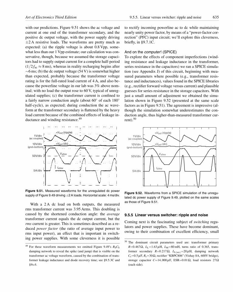
Art of Electronics Third Edition 9.5.5. Linear versus switcher: ripple and noise 635
with our predictions. Figure 9.51 shows the ac voltage andcurrent at one end of the transformer secondary, and thepositive dc output voltage, with the power supply driving±2 A resistive loads. The waveforms are pretty much asexpected: (a) the ripple voltage is about 0.8 Vpp, some-what less than our 1 Vpp estimate; our calculation was con-servative, though, because we assumed the storage capaci-tors had to supply output current for a complete half-period(1/2 fac ≈ 8 ms), whereas in reality recharging begins after∼6 ms; (b) the dc output voltage (54 V) is somewhat higherthan expected, probably because the transformer voltagerating is for the full-rated load current of 4 A, and also be-cause the powerline voltage in our lab was 3% above nom-inal; with no load the output rose to 60 V, typical of unreg-ulated supplies; (c) the transformer current is confined toa fairly narrow conduction angle (about 60◦ of each 180◦half-cycle), as expected; during conduction the ac wave-form at the transformer secondary is flattened by the heavyload current because of the combined effects of leakage in-ductance and winding resistance.49
+Vout (ripple)
+Vout (dc)
Vxfmr
Ixfmr
1V/div(ac coupled)
10V/div(gnd=bottom)
50V/div
5A/div
Figure 9.51. Measured waveforms for the unregulated dc powersupply of Figure 9.49 driving ±2 A loads. Horizontal scale: 4 ms/div.
With a 2 A dc load on both outputs, the measuredrms transformer current was 3.95 Arms. This doubling iscaused by the shortened conduction angle: the averagetransformer current equals the dc output current, but therms current is greater. This is sometimes described as a re-duced power factor (the ratio of average input power torms input power), an effect that is important in switch-ing power supplies. With some cleverness it is possible
49 For these waveform measurements we omitted Figure 9.49’s RSCS
damping network to reveal the spike (and jump) that is visible on thetransformer ac voltage waveform, caused by the combination of trans-former leakage inductance and diode recovery time; see §9.5.3C and§9x.6.
to rectify incoming powerline ac to dc while maintainingnearly unity power factor, by means of a “power-factor cor-rection” (PFC) input circuit; we’ll explore this cleverness,briefly, in §9.7.1C.
And on the computer ! (SPICE)To explore the effects of component imperfections (wind-ing resistance and leakage inductance in the transformer,series resistance in the capacitors) we ran a SPICE simula-tion (see Appendix J) of this circuit, beginning with mea-sured parameters where possible (e.g., transformer resis-tance and inductances), values found in the SPICE libraries(e.g., rectifier forward voltage versus current) and plausibleguesses for series resistance in the storage capacitors. Withjust a small amount of adjustment we obtained the simu-lation shown in Figure 9.52 (presented at the same scalefactors as in Figure 9.51). The agreement is impressive (al-though the simulation somewhat underestimates the con-duction angle, thus higher-than-measured transformer cur-rent).50
+Vout (ripple)
+Vout (dc)
Vxfmr
Ixfmr
1V/div(ac coupled)
10V/div(gnd=bottom)
50V/div
5A/div
Figure 9.52. Waveforms from a SPICE simulation of the unregu-lated dc power supply of Figure 9.49, plotted on the same scalesas those of Figure 9.51.
9.5.5 Linear versus switcher: ripple and noise
Coming next is the fascinating subject of switching regu-lators and power supplies. These have become dominant,owing to their combination of excellent efficiency, small
50 The dominant circuit parameters used are: transformer primaryR=0.467Ω, LL=1.63 μH, LM=80 mH, turns ratio of 0.365, trans-former secondary R=0.217Ω, LL(sec)=20 μH, damping networkCs=0.5 μF, Rs=30Ω, rectifier “KBPC806” (Vishay 8A, 600V bridge),storage capacitor C=14,000 μF, ESR=0.01Ω, load resistors 27Ω(each side).
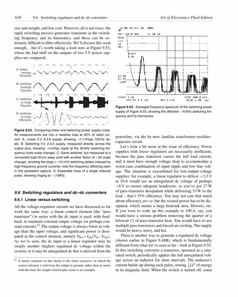
636 9.6. Switching regulators and dc–dc converters Art of Electronics Third Edition
size and weight, and low cost. However, all is not roses: therapid switching process generates transients at the switch-ing frequency and its harmonics, and these can be ex-tremely difficult to filter effectively. We’ll discuss this soonenough. . . but it’s worth taking a look now at Figure 9.53,where the bad stuff on the outputs of two 5 V power sup-plies are compared.
A. linear:1mV/div
10ms/div
B. switcher:
C. switcher:
D. switcher:
5mV/div10μs/div
0.1V/div10μs/div
0.1V/div100ns/div
Figure 9.53. Comparing linear and switching power supply noise.All measurements are into a resistive load at 50% of rated cur-rent. A. Linear 5 V, 0.3 A supply, showing ∼0.5 mVpp 120 Hz rip-ple. B. Switching 5 V, 2.5 A supply, measured directly across theoutput pins, showing ∼6 mVpp ripple at the 50 kHz switching fre-quency (note scale change). C. Same switcher, but measured at aconnected load 50 cm away (and with another factor of ×20 scalechange), showing the large (∼150 mV) switching spikes induced byhigh-frequency ground currents; note the frequency dithering seenin this persistent capture. D. Expanded trace of a single inducedpulse, showing ringing at ∼15 MHz.
9.6 Switching regulators and dc–dc converters
9.6.1 Linear versus switching
All the voltage-regulator circuits we have discussed so farwork the same way: a linear control element (the “passtransistor”) in series with the dc input is used, with feed-back, to maintain constant output voltage (or perhaps con-stant current).51 The output voltage is always lower in volt-age than the input voltage, and significant power is dissi-pated in the control element, namely Pdiss=Iout(Vin−Vout).As we’ve seen, the dc input to a linear regulator may besimply another (higher) regulated dc voltage within thesystem; or it may be unregulated dc that is derived from the
51 A minor variation on this theme is the shunt regulator, in which thecontrol element is tied from the output to ground, rather than in serieswith the load; the simple resistor-plus-zener is an example.
Figure 9.54. Averaged frequency spectrum of the switching powersupply of Figure 9.53, showing the dithered ∼50 kHz switching fre-quency and its harmonics.
powerline, via the by-now familiar transformer–rectifier–capacitor circuit.
Let’s look a bit more at the issue of efficiency. Powersupplies with linear regulators are necessarily inefficient,because the pass transistor carries the full load current,and it must have enough voltage drop to accommodate aworst-case combination of input ripple and low line volt-age. The situation is exacerbated for low-output-voltagesupplies: for example, a linear regulator to deliver +3.3 Vat 10 A would use an unregulated dc voltage of perhaps+6 V to ensure adequate headroom; so you’ve got 27 Wof pass-transistor dissipation while delivering 33 W to theload – that’s 55% efficiency. You may not care that muchabout efficiency per se; but the wasted power has to be dis-sipated, which means a large heatsink area, blowers, etc.If you were to scale up this example to 100 A, say, youwould have a serious problem removing the quarter of akilowatt (!) of pass-transistor heat. You would have to usemultiple pass transistors and forced-air cooling. The supplywould be heavy, noisy, and hot.
There is another way to generate a regulated dc voltage(shown earlier in Figure 9.48B), which is fundamentallydifferent from what we’ve seen so far – look at Figure 9.55.In this switching converter a transistor, operated as a satu-rated switch, periodically applies the full unregulated volt-age across an inductor for short intervals. The inductor’scurrent builds up during each pulse, storing 1
2 LI2 of energyin its magnetic field. When the switch is turned off, some
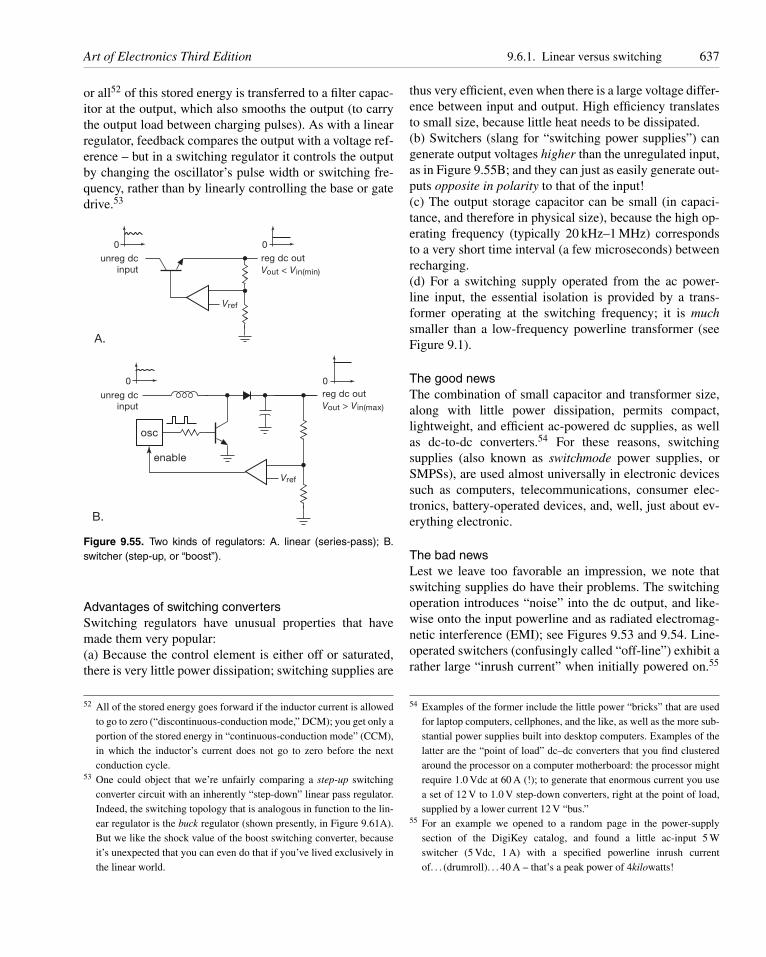
Art of Electronics Third Edition 9.6.1. Linear versus switching 637
or all52 of this stored energy is transferred to a filter capac-itor at the output, which also smooths the output (to carrythe output load between charging pulses). As with a linearregulator, feedback compares the output with a voltage ref-erence – but in a switching regulator it controls the outputby changing the oscillator’s pulse width or switching fre-quency, rather than by linearly controlling the base or gatedrive.53
unreg dc
input
unreg dc
input
reg dc out
Vout < Vin(min)
00
A.
Vref
reg dc out
Vout > Vin(max)
00
B.
osc
enable
Vref
Figure 9.55. Two kinds of regulators: A. linear (series-pass); B.switcher (step-up, or “boost”).
Advantages of switching convertersSwitching regulators have unusual properties that havemade them very popular:(a) Because the control element is either off or saturated,there is very little power dissipation; switching supplies are
52 All of the stored energy goes forward if the inductor current is allowedto go to zero (“discontinuous-conduction mode,” DCM); you get only aportion of the stored energy in “continuous-conduction mode” (CCM),in which the inductor’s current does not go to zero before the nextconduction cycle.
53 One could object that we’re unfairly comparing a step-up switchingconverter circuit with an inherently “step-down” linear pass regulator.Indeed, the switching topology that is analogous in function to the lin-ear regulator is the buck regulator (shown presently, in Figure 9.61A).But we like the shock value of the boost switching converter, becauseit’s unexpected that you can even do that if you’ve lived exclusively inthe linear world.
thus very efficient, even when there is a large voltage differ-ence between input and output. High efficiency translatesto small size, because little heat needs to be dissipated.(b) Switchers (slang for “switching power supplies”) cangenerate output voltages higher than the unregulated input,as in Figure 9.55B; and they can just as easily generate out-puts opposite in polarity to that of the input!(c) The output storage capacitor can be small (in capaci-tance, and therefore in physical size), because the high op-erating frequency (typically 20 kHz–1 MHz) correspondsto a very short time interval (a few microseconds) betweenrecharging.(d) For a switching supply operated from the ac power-line input, the essential isolation is provided by a trans-former operating at the switching frequency; it is muchsmaller than a low-frequency powerline transformer (seeFigure 9.1).
The good newsThe combination of small capacitor and transformer size,along with little power dissipation, permits compact,lightweight, and efficient ac-powered dc supplies, as wellas dc-to-dc converters.54 For these reasons, switchingsupplies (also known as switchmode power supplies, orSMPSs), are used almost universally in electronic devicessuch as computers, telecommunications, consumer elec-tronics, battery-operated devices, and, well, just about ev-erything electronic.
The bad newsLest we leave too favorable an impression, we note thatswitching supplies do have their problems. The switchingoperation introduces “noise” into the dc output, and like-wise onto the input powerline and as radiated electromag-netic interference (EMI); see Figures 9.53 and 9.54. Line-operated switchers (confusingly called “off-line”) exhibit arather large “inrush current” when initially powered on.55
54 Examples of the former include the little power “bricks” that are usedfor laptop computers, cellphones, and the like, as well as the more sub-stantial power supplies built into desktop computers. Examples of thelatter are the “point of load” dc–dc converters that you find clusteredaround the processor on a computer motherboard: the processor mightrequire 1.0 Vdc at 60 A (!); to generate that enormous current you usea set of 12 V to 1.0 V step-down converters, right at the point of load,supplied by a lower current 12 V “bus.”
55 For an example we opened to a random page in the power-supplysection of the DigiKey catalog, and found a little ac-input 5 Wswitcher (5 Vdc, 1 A) with a specified powerline inrush currentof. . . (drumroll). . . 40 A – that’s a peak power of 4kilowatts!
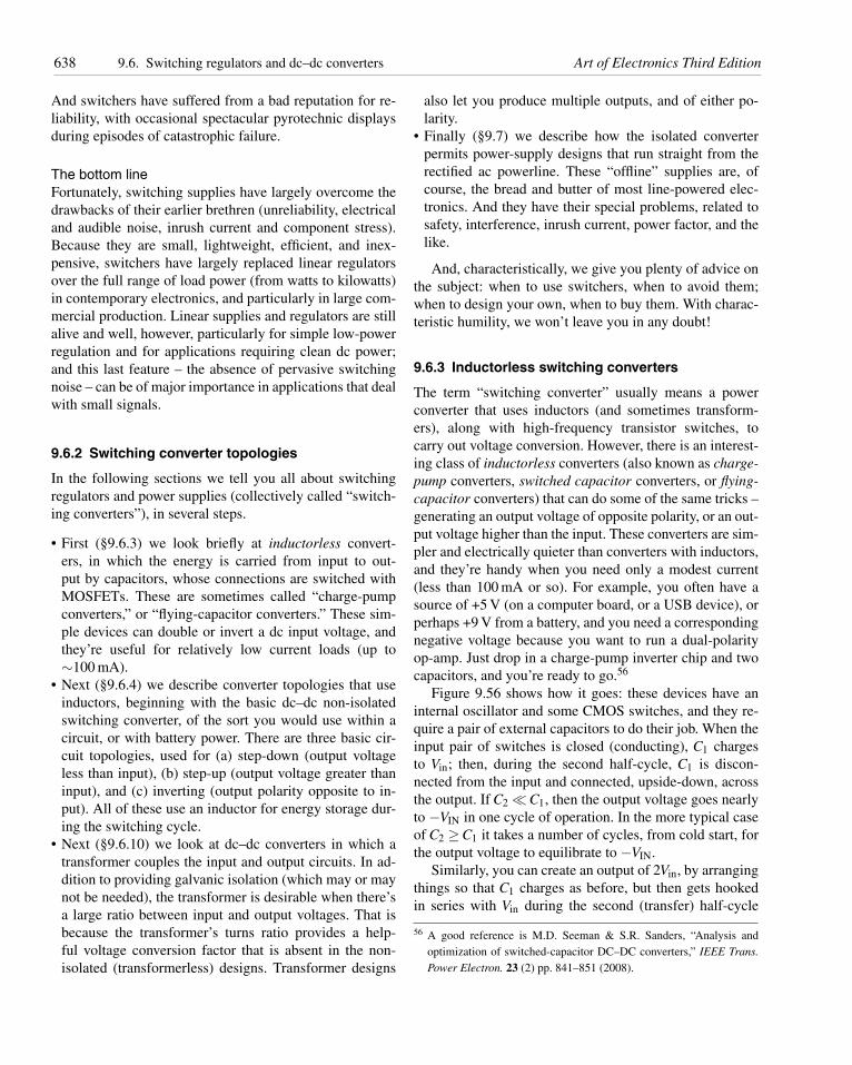
638 9.6. Switching regulators and dc–dc converters Art of Electronics Third Edition
And switchers have suffered from a bad reputation for re-liability, with occasional spectacular pyrotechnic displaysduring episodes of catastrophic failure.
The bottom lineFortunately, switching supplies have largely overcome thedrawbacks of their earlier brethren (unreliability, electricaland audible noise, inrush current and component stress).Because they are small, lightweight, efficient, and inex-pensive, switchers have largely replaced linear regulatorsover the full range of load power (from watts to kilowatts)in contemporary electronics, and particularly in large com-mercial production. Linear supplies and regulators are stillalive and well, however, particularly for simple low-powerregulation and for applications requiring clean dc power;and this last feature – the absence of pervasive switchingnoise – can be of major importance in applications that dealwith small signals.
9.6.2 Switching converter topologies
In the following sections we tell you all about switchingregulators and power supplies (collectively called “switch-ing converters”), in several steps.
• First (§9.6.3) we look briefly at inductorless convert-ers, in which the energy is carried from input to out-put by capacitors, whose connections are switched withMOSFETs. These are sometimes called “charge-pumpconverters,” or “flying-capacitor converters.” These sim-ple devices can double or invert a dc input voltage, andthey’re useful for relatively low current loads (up to∼100 mA).
• Next (§9.6.4) we describe converter topologies that useinductors, beginning with the basic dc–dc non-isolatedswitching converter, of the sort you would use within acircuit, or with battery power. There are three basic cir-cuit topologies, used for (a) step-down (output voltageless than input), (b) step-up (output voltage greater thaninput), and (c) inverting (output polarity opposite to in-put). All of these use an inductor for energy storage dur-ing the switching cycle.
• Next (§9.6.10) we look at dc–dc converters in which atransformer couples the input and output circuits. In ad-dition to providing galvanic isolation (which may or maynot be needed), the transformer is desirable when there’sa large ratio between input and output voltages. That isbecause the transformer’s turns ratio provides a help-ful voltage conversion factor that is absent in the non-isolated (transformerless) designs. Transformer designs
also let you produce multiple outputs, and of either po-larity.
• Finally (§9.7) we describe how the isolated converterpermits power-supply designs that run straight from therectified ac powerline. These “offline” supplies are, ofcourse, the bread and butter of most line-powered elec-tronics. And they have their special problems, related tosafety, interference, inrush current, power factor, and thelike.
And, characteristically, we give you plenty of advice onthe subject: when to use switchers, when to avoid them;when to design your own, when to buy them. With charac-teristic humility, we won’t leave you in any doubt!
9.6.3 Inductorless switching converters
The term “switching converter” usually means a powerconverter that uses inductors (and sometimes transform-ers), along with high-frequency transistor switches, tocarry out voltage conversion. However, there is an interest-ing class of inductorless converters (also known as charge-pump converters, switched capacitor converters, or flying-capacitor converters) that can do some of the same tricks –generating an output voltage of opposite polarity, or an out-put voltage higher than the input. These converters are sim-pler and electrically quieter than converters with inductors,and they’re handy when you need only a modest current(less than 100 mA or so). For example, you often have asource of +5 V (on a computer board, or a USB device), orperhaps +9 V from a battery, and you need a correspondingnegative voltage because you want to run a dual-polarityop-amp. Just drop in a charge-pump inverter chip and twocapacitors, and you’re ready to go.56
Figure 9.56 shows how it goes: these devices have aninternal oscillator and some CMOS switches, and they re-quire a pair of external capacitors to do their job. When theinput pair of switches is closed (conducting), C1 chargesto Vin; then, during the second half-cycle, C1 is discon-nected from the input and connected, upside-down, acrossthe output. If C2 �C1, then the output voltage goes nearlyto −VIN in one cycle of operation. In the more typical caseof C2 ≥C1 it takes a number of cycles, from cold start, forthe output voltage to equilibrate to −VIN.
Similarly, you can create an output of 2Vin, by arrangingthings so that C1 charges as before, but then gets hookedin series with Vin during the second (transfer) half-cycle
56 A good reference is M.D. Seeman & S.R. Sanders, “Analysis andoptimization of switched-capacitor DC–DC converters,” IEEE Trans.
Power Electron. 23 (2) pp. 841–851 (2008).
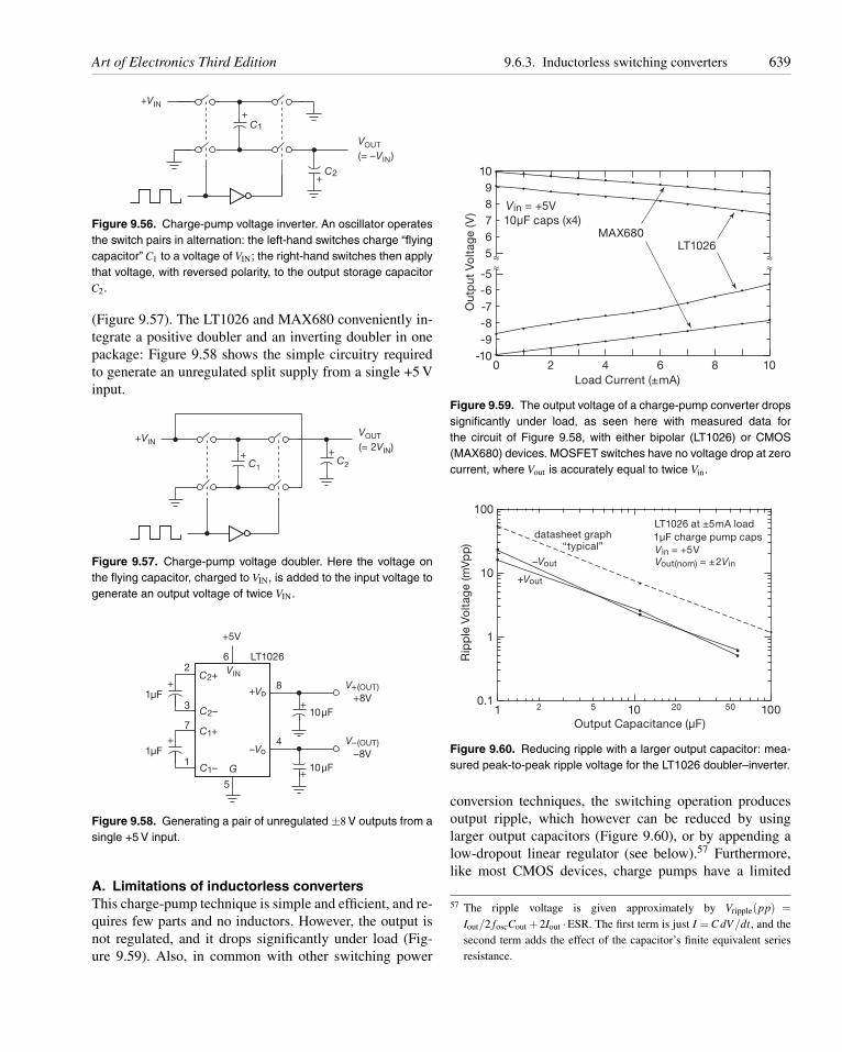
Art of Electronics Third Edition 9.6.3. Inductorless switching converters 639
VOUT
(= –VIN)
C1
+
+VIN
C2+
Figure 9.56. Charge-pump voltage inverter. An oscillator operatesthe switch pairs in alternation: the left-hand switches charge “flyingcapacitor” C1 to a voltage of VIN; the right-hand switches then applythat voltage, with reversed polarity, to the output storage capacitorC2.
(Figure 9.57). The LT1026 and MAX680 conveniently in-tegrate a positive doubler and an inverting doubler in onepackage: Figure 9.58 shows the simple circuitry requiredto generate an unregulated split supply from a single +5 Vinput.
C1
+
+VINVOUT
(= 2VIN)
C2
+
Figure 9.57. Charge-pump voltage doubler. Here the voltage onthe flying capacitor, charged to VIN, is added to the input voltage togenerate an output voltage of twice VIN.
1μF+
+
2
+5V
6
G
5
LT1026
VIN
V+(OUT)
+8V
V–(OUT)
–8V
+Vo
–Vo
C2+
C2–
C1–
C1+
3
1μF
10μF
+
7
4
1
+10μF
8
Figure 9.58. Generating a pair of unregulated ±8 V outputs from asingle +5 V input.
A. Limitations of inductorless convertersThis charge-pump technique is simple and efficient, and re-quires few parts and no inductors. However, the output isnot regulated, and it drops significantly under load (Fig-ure 9.59). Also, in common with other switching power
-10
-5-6-7-8-9
56789
10
Out
put
Vo
ltag
e (V
)
1086420Load Current (±mA)
LT1026MAX680
10μF caps (x4)Vin = +5V
≈≈
≈≈
Figure 9.59. The output voltage of a charge-pump converter dropssignificantly under load, as seen here with measured data forthe circuit of Figure 9.58, with either bipolar (LT1026) or CMOS(MAX680) devices. MOSFET switches have no voltage drop at zerocurrent, where Vout is accurately equal to twice Vin.
0.1
1
10
100
Rip
ple
Vo
ltag
e (m
Vp
p)
1 2 5 10 20 50 100Output Capacitance (μF)
+Vout
–Vout
LT1026 at ±5mA load1μF charge pump capsVin = +5VVout(nom) = ±2Vin
datasheet graph“typical”
Figure 9.60. Reducing ripple with a larger output capacitor: mea-sured peak-to-peak ripple voltage for the LT1026 doubler–inverter.
conversion techniques, the switching operation producesoutput ripple, which however can be reduced by usinglarger output capacitors (Figure 9.60), or by appending alow-dropout linear regulator (see below).57 Furthermore,like most CMOS devices, charge pumps have a limited
57 The ripple voltage is given approximately by Vripple(pp) =Iout/2 foscCout +2Iout ·ESR. The first term is just I = C dV/dt, and thesecond term adds the effect of the capacitor’s finite equivalent seriesresistance.
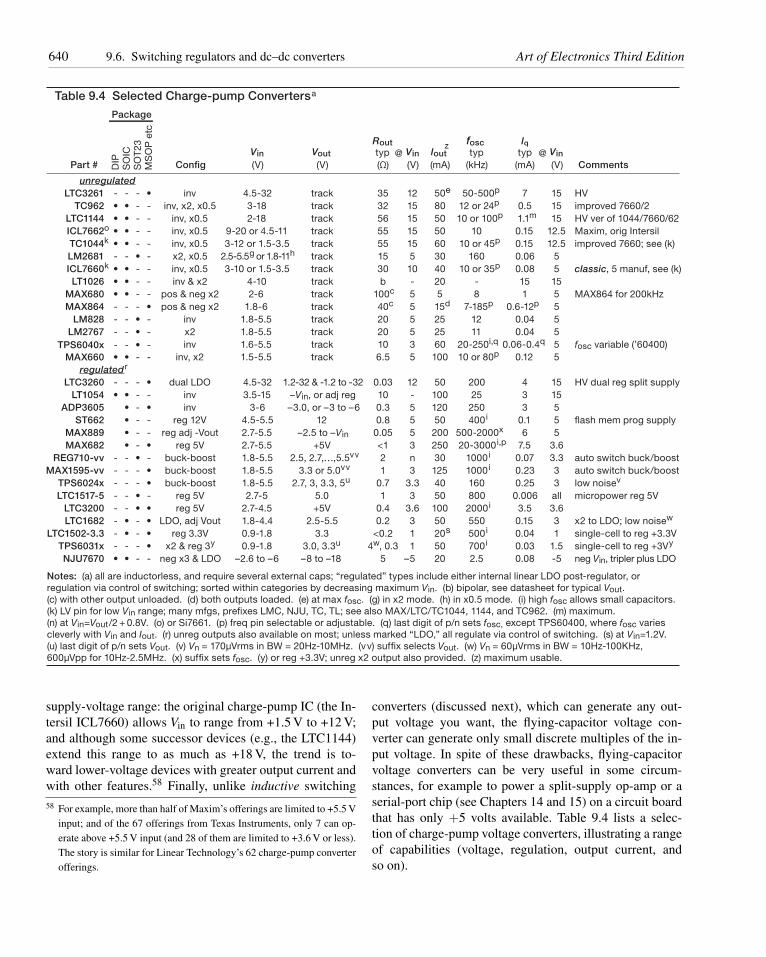
640 9.6. Switching regulators and dc–dc converters Art of Electronics Third Edition
TC1044k • • - - inv, x0.5 3-12 or 1.5-3.5 track 55 15 60 10 or 45p 0.15 12.5 improved 7660; see (k)
LM2681 - - • - x2, x0.5 2.5-5.5g or 1.8-11h track 15 5 30 160 0.06 5
ICL7660k • • - - inv, x0.5 3-10 or 1.5-3.5 track 30 10 40 10 or 35p 0.08 5 classic, 5 manuf, see (k)
LT1026 • • - - inv & x2 4-10 track b - 20 - 15 15
MAX680 • • - - pos & neg x2 2-6 track 100c 5 5 8 1 5 MAX864 for 200kHz
MAX864 - - - • pos & neg x2 1.8-6 track 40c 5 15d 7-185p 0.6-12p 5
LM828 - - • - inv 1.8-5.5 track 20 5 25 12 0.04 5
LM2767 - - • - x2 1.8-5.5 track 20 5 25 11 0.04 5
inv 1.6-5.5 track 10 3 60 20-250i,q 0.06-0.4q 5TPS6040x - - • -
inv, x2 1.5-5.5 track 6.5 5 100 10 or 80p 0.12 5
regulatedr
LTC3260 - - - • dual LDO 4.5-32 1.2-32 & -1.2 to -32 0.03 12 50 200 4 15 HV dual reg split supply
LT1054 • • - - inv 3.5-15 –Vin, or adj reg 10 - 100 25 3 15
ADP3605 • - • inv 3-6 –3.0, or –3 to –6 0.3 5 120 250 3 5
ST662 • - - reg 12V 4.5-5.5 12 0.8 5 50 400i 0.1 5 flash mem prog supply
fosc variable (’60400)
MAX889 • - - reg adj -Vout 2.7-5.5 –2.5 to –Vin 0.05 5 200 500-2000x 6 5
MAX682 • - • reg 5V 2.7-5.5 +5V <1 3 250 20-3000i,p 7.5 3.6
REG710-vv - - • - buck-boost 1.8-5.5 2.5, 2.7,…,5.5vv 2 n 30 1000i 0.07 3.3 auto switch buck/boost
MAX1595-vv - - - • buck-boost 1.8-5.5 3.3 or 5.0vv 1 3 125 1000i 0.23 3 auto switch buck/boost
TPS6024x - - - • buck-boost 1.8-5.5 2.7, 3, 3.3, 5u 0.7 3.3 40 160 0.25 3 low noisev
LTC1517-5 - - • - reg 5V 2.7-5 5.0 1 3 50 800 0.006 all micropower reg 5V
LTC3200 - - • • reg 5V 2.7-4.5 +5V 0.4 3.6 100 2000i 3.5 3.6
LTC1682 - • - • LDO, adj Vout 1.8-4.4 2.5-5.5 0.2 3 50 550 0.15 3 x2 to LDO; low noisew
LTC1502-3.3 - • - • reg 3.3V 0.9-1.8 3.3 <0.2 1 20s 500i 0.04 1 single-cell to reg +3.3V
TPS6031x - - - • x2 & reg 3y 0.9-1.8 3.0, 3.3u 4w, 0.3 1 50 700i 0.03 1.5 single-cell to reg +3V y
NJU7670 • • - - neg x3 & LDO –2.6 to –6 –8 to –18 5 –5 20 2.5 0.08 -5 neg Vin, tripler plus LDO
Notes: (a) all are inductorless, and require several external caps; “regulated” types include either internal linear LDO post-regulator, or
regulation via control of switching; sorted within categories by decreasing maximum Vin. (b) bipolar, see datasheet for typical Vout.
(c) with other output unloaded. (d) both outputs loaded. (e) at max fosc. (g) in x2 mode. (h) in x0.5 mode. (i) high fosc allows small capacitors.
(k) LV pin for low Vin range; many mfgs, prefixes LMC, NJU, TC, TL; see also MAX/LTC/TC1044, 1144, and TC962. (m) maximum.
(n) at Vin=Vout/2 + 0.8V. (o) or Si7661. (p) freq pin selectable or adjustable. (q) last digit of p/n sets fosc, except TPS60400, where fosc varies
cleverly with Vin and Iout. (r) unreg outputs also available on most; unless marked “LDO,” all regulate via control of switching. (s) at Vin=1.2V.
(u) last digit of p/n sets Vout. (v) Vn = 170μVrms in BW = 20Hz-10MHz. (vv) suffix selects Vout. (w) Vn = 60μVrms in BW = 10Hz-100KHz,
600μVpp for 10Hz-2.5MHz. (x) suffix sets fosc. (y) or reg +3.3V; unreg x2 output also provided. (z) maximum usable.
Table 9.4 Selected Charge-pump Convertersa
DIP
SO
ICS
OT
23
MS
OP
etc
Rout
Part #
Package
Config
Vin VinVout
fosc
typ typ typ
Iq
Comments(V) (V) (Ω) (V)
@ Vin@
(mA) (kHz) (mA) (V)
unregulatedLTC3261 - - - • inv 4.5-32 track 35 12 50e 50-500p 7
Ioutz
15 HV
TC962 • • - - inv, x2, x0.5 3-18 track 32 15 80 12 or 24p 0.5 15 improved 7660/2
LTC1144 • • - - inv, x0.5 2-18 track 56 15 50 10 or 100p 1.1m 15 HV ver of 1044/7660/62
ICL7662o • • - - inv, x0.5 9-20 or 4.5-11 track 55 15 50 10 0.15 12.5 Maxim, orig Intersil
MAX660 • • - -
supply-voltage range: the original charge-pump IC (the In-tersil ICL7660) allows Vin to range from +1.5 V to +12 V;and although some successor devices (e.g., the LTC1144)extend this range to as much as +18 V, the trend is to-ward lower-voltage devices with greater output current andwith other features.58 Finally, unlike inductive switching58 For example, more than half of Maxim’s offerings are limited to +5.5 V
input; and of the 67 offerings from Texas Instruments, only 7 can op-erate above +5.5 V input (and 28 of them are limited to +3.6 V or less).The story is similar for Linear Technology’s 62 charge-pump converterofferings.
converters (discussed next), which can generate any out-put voltage you want, the flying-capacitor voltage con-verter can generate only small discrete multiples of the in-put voltage. In spite of these drawbacks, flying-capacitorvoltage converters can be very useful in some circum-stances, for example to power a split-supply op-amp or aserial-port chip (see Chapters 14 and 15) on a circuit boardthat has only +5 volts available. Table 9.4 lists a selec-tion of charge-pump voltage converters, illustrating a rangeof capabilities (voltage, regulation, output current, andso on).
Art of Electronics Third Edition 9.6.4. Converters with inductors: the basic non-isolated topologies 641
B. VariationsThere are interesting and useful flying-capacitor variations,many of which are listed in Table 9.4, which is orga-nized into unregulated and regulated varieties (each sortedby maximum input voltage). The unregulated types repre-sent variations on the original ICL7660, including its simi-larly named successors (from TI, NJR, Maxim, Microchip,etc.) and pin-compatible upgrades (’7662, ’1044, ’1144);such multiply-sourced jellybean parts are widely availableand inexpensive. More recent parts, for example the low-voltage TPS6040x, offer flexibility in switching frequency,and generally lower output resistance. Operation at higherfrequency reduces output ripple (e.g., 35 mV at 20 kHz, but15 mV at 250 kHz for the TPS6040x series), but it increasesquiescent current (which goes from 65 μA to 425 μA inthis example).59
The regulated types, like the LT1054 from LTC (with amaximum output current of 100 mA), include an internalvoltage reference and error amplifier, so you can connectfeedback to regulate the output voltage; the internal cir-cuitry accommodates this by adjusting the switching con-trol. Other converters regulate the output by including aninternal low-dropout linear regulator, for greatly reducedoutput ripple (at the expense of some additional voltagedrop); examples are the LTC1550 and 1682 series, withless than 1 mV peak-to-peak output ripple. Note that mostof the “regulated” types let you use them as unregulatedconverters, if you wish.
There are also converters that reduce the input voltageby a rational fraction, e.g., by a factor of 1/2 or 2/3 (seeif you can figure out how that is done!). At the other end,there are converters that are voltage quadruplers, for ex-ample the LTC1502, which generates a regulated +3.3 V at10 mA from an input of 0.9–1.8 V (e.g., to power digitallogic from a single alkaline cell).60 And there are convert-
59 You can reduce ripple by using much larger output capacitors (withlow ESR, to minimize the effect of current spikes), or, perhaps better,an output filter stage.
60 Sadly, there are no charge-pump converters that take a single-cell input(0.9 V at end of life) up to +5 V (that would require at least a ×6 voltageconversion), although you could accomplish that task in two steps bycascading, say, a TPS60310 (0.9–3.3 V) with a TPS60241 (3.3–5 V).That would require two ICs and seven capacitors. But, happily, sucha task is easily done with a boost-mode inductive switching converter(§9.6.6). For example, TI’s TPS61222 comes in a tiny 6-pin SC-70package, requires only a single external 4.7 μH inductor (plus inputand output bypass caps), and delivers +5 V at 50 mA with 0.9 V input(an alkaline cell’s end-of-life voltage). It costs less than $2 in single-piece quantities. Another approach to powering from a single alkalinecell is to use a charge-pump converter to generate +3.3 V, which then
ers that can provide up to 500 mA of output current. Somecharge-pump converters include internal capacitors, if youwant to be especially lazy; but the selection is limited, andthe price is high.
Finally, there is the LTC1043 uncommitted flying-capacitor building block, with which you can do all kindsof magic. For example, you can use a flying capacitor totransfer a voltage drop measured at an inconvenient poten-tial (e.g., a current-sensing resistor at the positive supplyvoltage) down to ground, where you can easily use it. TheLTC1043 datasheet has eight pages of similarly clever ap-plications.
Then there are integrated circuits that include chargepumps to power their primary functions:(a) Many RS-232/485 driver–receiver chips are availablewith integral ±10 V charge-pump supplies, to run froma single +5 V or +3.3 V supply. An example of the lat-ter is the MAX3232E from Maxim (the originator of theMAX232, now widely second sourced), which can runfrom a single supply between +3 V and +5.5 V.(b) Some op-amps use integral charge pumps to gener-ate a voltage beyond the supply rail, so their inputs canoperate rail-to-rail while maintaining a conventional high-performance architecture (see §4.6.3B); examples are theOPA369, LTC1152, and MAX1462-4.(c) Charge pumps are used in many MOSFET “high-sidedrivers” (like the HIP4080 series from Intersil) and in fullyintegrated power MOSFETs (like the PROFET series of“smart highside high-current power switches” from Infi-neon); these generate the necessary above-the-rail gate biasfor an n-channel MOSFET operating as a follower up at thepositive rail.61
(d) Some complex digital logic devices (processors, mem-ory) require elevated voltages, which they generate on-chipwith charge pumps. The manufacturers are modest, andyou don’t even hear about these things.
9.6.4 Converters with inductors: the basicnon-isolated topologies
The term switching converter (or switchmode converter62)is generally understood to mean a converter that uses somearrangement of inductors and/or transformers, in combina-tion with transistor switches (usually MOSFETs, but also
powers one or more inductive switching converters to generate the fullset of voltages you need; the ENABLE input to the charge-pump con-verter can then be used to turn power on or off.
61 For further detail see §3.5.3 and Figures 3.96 and 3.106.62 Switchmode power supplies are referred to as SMPSs, thus phrases like
“SMPS technology.”
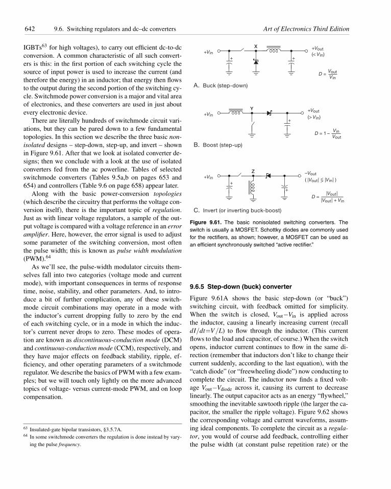
642 9.6. Switching regulators and dc–dc converters Art of Electronics Third Edition
IGBTs63 for high voltages), to carry out efficient dc-to-dcconversion. A common characteristic of all such convert-ers is this: in the first portion of each switching cycle thesource of input power is used to increase the current (andtherefore the energy) in an inductor; that energy then flowsto the output during the second portion of the switching cy-cle. Switchmode power conversion is a major and vital areaof electronics, and these converters are used in just aboutevery electronic device.
There are literally hundreds of switchmode circuit vari-ations, but they can be pared down to a few fundamentaltopologies. In this section we describe the three basic non-isolated designs – step-down, step-up, and invert – shownin Figure 9.61. After that we look at isolated converter de-signs; then we conclude with a look at the use of isolatedconverters fed from the ac powerline. Tables of selectedswitchmode converters (Tables 9.5a,b on pages 653 and654) and controllers (Table 9.6 on page 658) appear later.
Along with the basic power-conversion topologies(which describe the circuitry that performs the voltage con-version itself), there is the important topic of regulation.Just as with linear voltage regulators, a sample of the out-put voltage is compared with a voltage reference in an erroramplifier. Here, however, the error signal is used to adjustsome parameter of the switching conversion, most oftenthe pulse width; this is known as pulse width modulation(PWM).64
As we’ll see, the pulse-width modulator circuits them-selves fall into two categories (voltage mode and currentmode), with important consequences in terms of responsetime, noise, stability, and other parameters. And, to intro-duce a bit of further complication, any of these switch-mode circuit combinations may operate in a mode withthe inductor’s current dropping fully to zero by the endof each switching cycle, or in a mode in which the induc-tor’s current never drops to zero. These modes of opera-tion are known as discontinuous-conduction mode (DCM)and continuous-conduction mode (CCM), respectively, andthey have major effects on feedback stability, ripple, ef-ficiency, and other operating parameters of a switchmoderegulator. We describe the basics of PWM with a few exam-ples; but we will touch only lightly on the more advancedtopics of voltage- versus current-mode PWM, and on loopcompensation.
63 Insulated-gate bipolar transistors, §3.5.7A.64 In some switchmode converters the regulation is done instead by vary-
ing the pulse frequency.
+Vin+Vout
(< Vin)+ +
X
A. Buck (step-down)
+Vin
+
+
Z
C. Invert (or inverting buck-boost)
+Vin+Vout
(> Vin)+
Y
B. Boost (step-up)
–Vout
( |Vout| >< |Vin| )
D =Vout
Vin
D = 1 –Vin
Vout
D =|Vout|
|Vout| + Vin
Figure 9.61. The basic nonisolated switching converters. Theswitch is usually a MOSFET. Schottky diodes are commonly usedfor the rectifiers, as shown; however, a MOSFET can be used asan efficient synchronously switched “active rectifier.”
9.6.5 Step-down (buck) converter
Figure 9.61A shows the basic step-down (or “buck”)switching circuit, with feedback omitted for simplicity.When the switch is closed, Vout−Vin is applied acrossthe inductor, causing a linearly increasing current (recalldI/dt=V/L) to flow through the inductor. (This currentflows to the load and capacitor, of course.) When the switchopens, inductor current continues to flow in the same di-rection (remember that inductors don’t like to change theircurrent suddenly, according to the last equation), with the“catch diode” (or “freewheeling diode”) now conducting tocomplete the circuit. The inductor now finds a fixed volt-age Vout−Vdiode across it, causing its current to decreaselinearly. The output capacitor acts as an energy “flywheel,”smoothing the inevitable sawtooth ripple (the larger the ca-pacitor, the smaller the ripple voltage). Figure 9.62 showsthe corresponding voltage and current waveforms, assum-ing ideal components. To complete the circuit as a regula-tor, you would of course add feedback, controlling eitherthe pulse width (at constant pulse repetition rate) or the
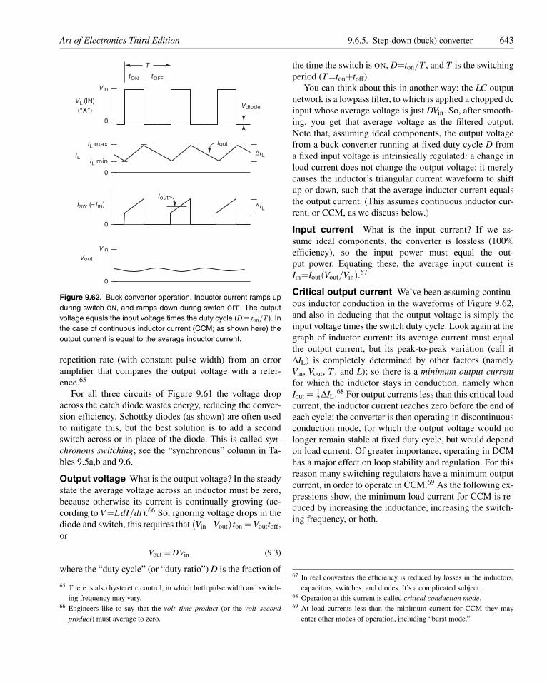
Art of Electronics Third Edition 9.6.5. Step-down (buck) converter 643
Vin
Vdiode
tON tOFF
VL (IN)
(“X”)
T
0
Vin
Vout
0
0
IL max
IL minIL
Iout
0
ISW (= IIN)
Iout
ΔIL
ΔIL
Figure 9.62. Buck converter operation. Inductor current ramps upduring switch ON, and ramps down during switch OFF. The outputvoltage equals the input voltage times the duty cycle (D ≡ ton/T ). Inthe case of continuous inductor current (CCM; as shown here) theoutput current is equal to the average inductor current.
repetition rate (with constant pulse width) from an erroramplifier that compares the output voltage with a refer-ence.65
For all three circuits of Figure 9.61 the voltage dropacross the catch diode wastes energy, reducing the conver-sion efficiency. Schottky diodes (as shown) are often usedto mitigate this, but the best solution is to add a secondswitch across or in place of the diode. This is called syn-chronous switching; see the “synchronous” column in Ta-bles 9.5a,b and 9.6.
Output voltage What is the output voltage? In the steadystate the average voltage across an inductor must be zero,because otherwise its current is continually growing (ac-cording to V=LdI/dt).66 So, ignoring voltage drops in thediode and switch, this requires that (Vin−Vout) ton =Vouttoff,or
Vout = DVin, (9.3)
where the “duty cycle” (or “duty ratio”) D is the fraction of
65 There is also hysteretic control, in which both pulse width and switch-ing frequency may vary.
66 Engineers like to say that the volt–time product (or the volt–secondproduct) must average to zero.
the time the switch is ON, D=ton/T , and T is the switchingperiod (T=ton+toff).
You can think about this in another way: the LC outputnetwork is a lowpass filter, to which is applied a chopped dcinput whose average voltage is just DVin. So, after smooth-ing, you get that average voltage as the filtered output.Note that, assuming ideal components, the output voltagefrom a buck converter running at fixed duty cycle D froma fixed input voltage is intrinsically regulated: a change inload current does not change the output voltage; it merelycauses the inductor’s triangular current waveform to shiftup or down, such that the average inductor current equalsthe output current. (This assumes continuous inductor cur-rent, or CCM, as we discuss below.)
Input current What is the input current? If we as-sume ideal components, the converter is lossless (100%efficiency), so the input power must equal the out-put power. Equating these, the average input current isIin=Iout(Vout/Vin).67
Critical output current We’ve been assuming continu-ous inductor conduction in the waveforms of Figure 9.62,and also in deducing that the output voltage is simply theinput voltage times the switch duty cycle. Look again at thegraph of inductor current: its average current must equalthe output current, but its peak-to-peak variation (call itΔIL) is completely determined by other factors (namelyVin, Vout, T , and L); so there is a minimum output currentfor which the inductor stays in conduction, namely whenIout = 1
2 ΔIL.68 For output currents less than this critical loadcurrent, the inductor current reaches zero before the end ofeach cycle; the converter is then operating in discontinuousconduction mode, for which the output voltage would nolonger remain stable at fixed duty cycle, but would dependon load current. Of greater importance, operating in DCMhas a major effect on loop stability and regulation. For thisreason many switching regulators have a minimum outputcurrent, in order to operate in CCM.69 As the following ex-pressions show, the minimum load current for CCM is re-duced by increasing the inductance, increasing the switch-ing frequency, or both.
67 In real converters the efficiency is reduced by losses in the inductors,capacitors, switches, and diodes. It’s a complicated subject.
68 Operation at this current is called critical conduction mode.69 At load currents less than the minimum current for CCM they may
enter other modes of operation, including “burst mode.”
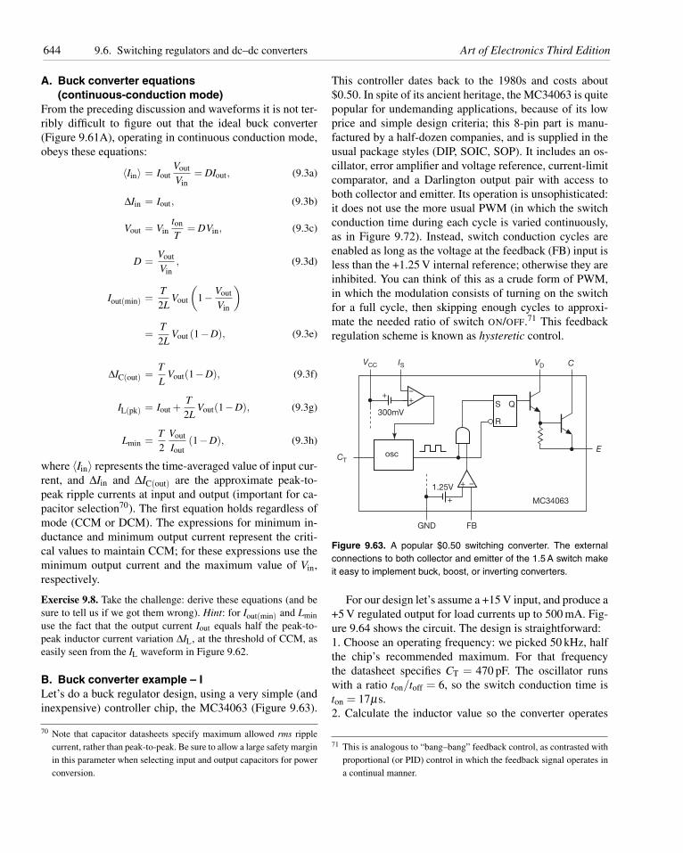
644 9.6. Switching regulators and dc–dc converters Art of Electronics Third Edition
A. Buck converter equations(continuous-conduction mode)
From the preceding discussion and waveforms it is not ter-ribly difficult to figure out that the ideal buck converter(Figure 9.61A), operating in continuous conduction mode,obeys these equations:
〈Iin〉 = IoutVout
Vin= DIout, (9.3a)
ΔIin = Iout, (9.3b)
Vout = Vinton
T= DVin, (9.3c)
D =Vout
Vin, (9.3d)
Iout(min) =T2L
Vout
(1− Vout
Vin
)
=T2L
Vout (1−D), (9.3e)
ΔIC(out) =TL
Vout(1−D), (9.3f)
IL(pk) = Iout +T2L
Vout(1−D), (9.3g)
Lmin =T2
Vout
Iout(1−D), (9.3h)
where 〈Iin〉 represents the time-averaged value of input cur-rent, and ΔIin and ΔIC(out) are the approximate peak-to-peak ripple currents at input and output (important for ca-pacitor selection70). The first equation holds regardless ofmode (CCM or DCM). The expressions for minimum in-ductance and minimum output current represent the criti-cal values to maintain CCM; for these expressions use theminimum output current and the maximum value of Vin,respectively.
Exercise 9.8. Take the challenge: derive these equations (and besure to tell us if we got them wrong). Hint: for Iout(min) and Lminuse the fact that the output current Iout equals half the peak-to-peak inductor current variation ΔIL, at the threshold of CCM, aseasily seen from the IL waveform in Figure 9.62.
B. Buck converter example – ILet’s do a buck regulator design, using a very simple (andinexpensive) controller chip, the MC34063 (Figure 9.63).
70 Note that capacitor datasheets specify maximum allowed rms ripplecurrent, rather than peak-to-peak. Be sure to allow a large safety marginin this parameter when selecting input and output capacitors for powerconversion.
This controller dates back to the 1980s and costs about$0.50. In spite of its ancient heritage, the MC34063 is quitepopular for undemanding applications, because of its lowprice and simple design criteria; this 8-pin part is manu-factured by a half-dozen companies, and is supplied in theusual package styles (DIP, SOIC, SOP). It includes an os-cillator, error amplifier and voltage reference, current-limitcomparator, and a Darlington output pair with access toboth collector and emitter. Its operation is unsophisticated:it does not use the more usual PWM (in which the switchconduction time during each cycle is varied continuously,as in Figure 9.72). Instead, switch conduction cycles areenabled as long as the voltage at the feedback (FB) input isless than the +1.25 V internal reference; otherwise they areinhibited. You can think of this as a crude form of PWM,in which the modulation consists of turning on the switchfor a full cycle, then skipping enough cycles to approxi-mate the needed ratio of switch ON/OFF.71 This feedbackregulation scheme is known as hysteretic control.
osc
MC34063
E
S
R
Q
C
1.25V
GND FB
+
+
+ –
–
300mV
+
CT
VCC VDIS
Figure 9.63. A popular $0.50 switching converter. The externalconnections to both collector and emitter of the 1.5 A switch makeit easy to implement buck, boost, or inverting converters.
For our design let’s assume a +15 V input, and produce a+5 V regulated output for load currents up to 500 mA. Fig-ure 9.64 shows the circuit. The design is straightforward:1. Choose an operating frequency: we picked 50 kHz, halfthe chip’s recommended maximum. For that frequencythe datasheet specifies CT = 470 pF. The oscillator runswith a ratio ton/toff = 6, so the switch conduction time iston = 17μs.2. Calculate the inductor value so the converter operates
71 This is analogous to “bang–bang” feedback control, as contrasted withproportional (or PID) control in which the feedback signal operates ina continual manner.
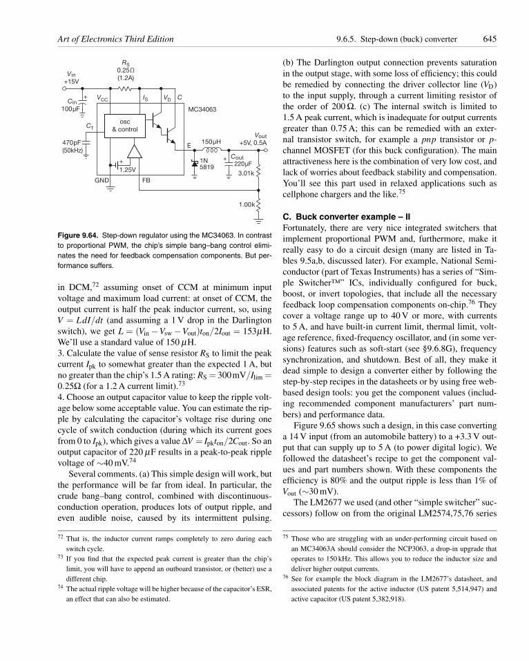
Art of Electronics Third Edition 9.6.5. Step-down (buck) converter 645
osc
& control
1N5819
MC34063
470pF
(50kHz)
C
1.25V3.01k
1.00k
FBGND
E
Vout
+5V, 0.5A
Vin
+15V
Cout
220μF
Cin
100μF
RS
0.25Ω
(1.2A)
150μH
+
++
CT
VCC VDIS
Figure 9.64. Step-down regulator using the MC34063. In contrastto proportional PWM, the chip’s simple bang–bang control elimi-nates the need for feedback compensation components. But per-formance suffers.
in DCM,72 assuming onset of CCM at minimum inputvoltage and maximum load current: at onset of CCM, theoutput current is half the peak inductor current, so, usingV = LdI/dt (and assuming a 1 V drop in the Darlingtonswitch), we get L = (Vin −Vsw −Vout)ton/2Iout = 153μH.We’ll use a standard value of 150 μH.3. Calculate the value of sense resistor RS to limit the peakcurrent Ipk to somewhat greater than the expected 1 A, butno greater than the chip’s 1.5 A rating: RS = 300mV/Ilim =0.25Ω (for a 1.2 A current limit).73
4. Choose an output capacitor value to keep the ripple volt-age below some acceptable value. You can estimate the rip-ple by calculating the capacitor’s voltage rise during onecycle of switch conduction (during which its current goesfrom 0 to Ipk), which gives a value ΔV = Ipkton/2Cout. So anoutput capacitor of 220 μF results in a peak-to-peak ripplevoltage of ∼40 mV.74
Several comments. (a) This simple design will work, butthe performance will be far from ideal. In particular, thecrude bang–bang control, combined with discontinuous-conduction operation, produces lots of output ripple, andeven audible noise, caused by its intermittent pulsing.
72 That is, the inductor current ramps completely to zero during eachswitch cycle.
73 If you find that the expected peak current is greater than the chip’slimit, you will have to append an outboard transistor, or (better) use adifferent chip.
74 The actual ripple voltage will be higher because of the capacitor’s ESR,an effect that can also be estimated.
(b) The Darlington output connection prevents saturationin the output stage, with some loss of efficiency; this couldbe remedied by connecting the driver collector line (VD)to the input supply, through a current limiting resistor ofthe order of 200 Ω. (c) The internal switch is limited to1.5 A peak current, which is inadequate for output currentsgreater than 0.75 A; this can be remedied with an exter-nal transistor switch, for example a pnp transistor or p-channel MOSFET (for this buck configuration). The mainattractiveness here is the combination of very low cost, andlack of worries about feedback stability and compensation.You’ll see this part used in relaxed applications such ascellphone chargers and the like.75
C. Buck converter example – IIFortunately, there are very nice integrated switchers thatimplement proportional PWM and, furthermore, make itreally easy to do a circuit design (many are listed in Ta-bles 9.5a,b, discussed later). For example, National Semi-conductor (part of Texas Instruments) has a series of “Sim-ple Switcher™” ICs, individually configured for buck,boost, or invert topologies, that include all the necessaryfeedback loop compensation components on-chip.76 Theycover a voltage range up to 40 V or more, with currentsto 5 A, and have built-in current limit, thermal limit, volt-age reference, fixed-frequency oscillator, and (in some ver-sions) features such as soft-start (see §9.6.8G), frequencysynchronization, and shutdown. Best of all, they make itdead simple to design a converter either by following thestep-by-step recipes in the datasheets or by using free web-based design tools: you get the component values (includ-ing recommended component manufacturers’ part num-bers) and performance data.
Figure 9.65 shows such a design, in this case convertinga 14 V input (from an automobile battery) to a +3.3 V out-put that can supply up to 5 A (to power digital logic). Wefollowed the datasheet’s recipe to get the component val-ues and part numbers shown. With these components theefficiency is 80% and the output ripple is less than 1% ofVout (∼30 mV).
The LM2677 we used (and other “simple switcher” suc-cessors) follow on from the original LM2574,75,76 series
75 Those who are struggling with an under-performing circuit based onan MC34063A should consider the NCP3063, a drop-in upgrade thatoperates to 150 kHz. This allows you to reduce the inductor size anddeliver higher output currents.
76 See for example the block diagram in the LM2677’s datasheet, andassociated patents for the active inductor (US patent 5,514,947) andactive capacitor (US patent 5,382,918).
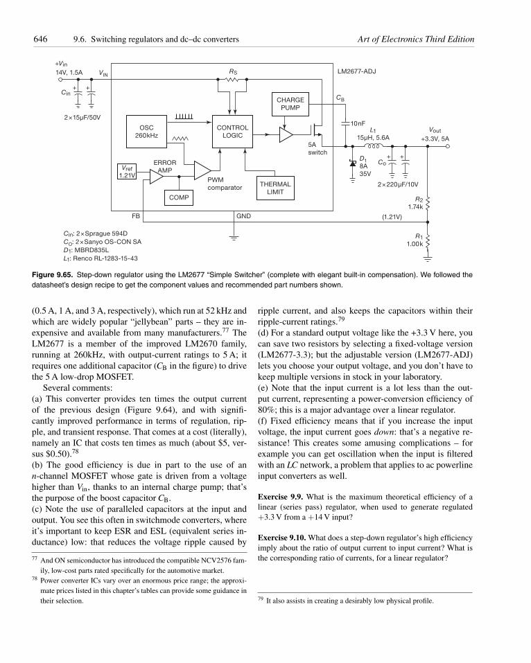
646 9.6. Switching regulators and dc–dc converters Art of Electronics Third Edition
OSC
260kHzVout
+3.3V, 5A
+Vin
Vref
1.21V
VIN
Cin: 2×Sprague 594D
CO: 2×Sanyo OS-CON SA
D1: MBRD835L
L1: Renco RL-1283-15-43
CB
D1
8A
35V
L1
15μH, 5.6A
R2
1.74k
R1
1.00k
+
CONTROL
LOGIC
RS
FB GND
PWM
comparator
5A
switch
ERROR
AMP
10nF
LM2677-ADJ
CHARGE
PUMP
THERMAL
LIMITCOMP
Cin+
++
14V, 1.5A
2×15μF/50V
Co
2×220μF/10V
(1.21V)
Figure 9.65. Step-down regulator using the LM2677 “Simple Switcher” (complete with elegant built-in compensation). We followed thedatasheet’s design recipe to get the component values and recommended part numbers shown.
(0.5 A, 1 A, and 3 A, respectively), which run at 52 kHz andwhich are widely popular “jellybean” parts – they are in-expensive and available from many manufacturers.77 TheLM2677 is a member of the improved LM2670 family,running at 260kHz, with output-current ratings to 5 A; itrequires one additional capacitor (CB in the figure) to drivethe 5 A low-drop MOSFET.
Several comments:(a) This converter provides ten times the output currentof the previous design (Figure 9.64), and with signifi-cantly improved performance in terms of regulation, rip-ple, and transient response. That comes at a cost (literally),namely an IC that costs ten times as much (about $5, ver-sus $0.50).78
(b) The good efficiency is due in part to the use of ann-channel MOSFET whose gate is driven from a voltagehigher than Vin, thanks to an internal charge pump; that’sthe purpose of the boost capacitor CB.(c) Note the use of paralleled capacitors at the input andoutput. You see this often in switchmode converters, whereit’s important to keep ESR and ESL (equivalent series in-ductance) low: that reduces the voltage ripple caused by
77 And ON semiconductor has introduced the compatible NCV2576 fam-ily, low-cost parts rated specifically for the automotive market.
78 Power converter ICs vary over an enormous price range; the approxi-mate prices listed in this chapter’s tables can provide some guidance intheir selection.
ripple current, and also keeps the capacitors within theirripple-current ratings.79
(d) For a standard output voltage like the +3.3 V here, youcan save two resistors by selecting a fixed-voltage version(LM2677-3.3); but the adjustable version (LM2677-ADJ)lets you choose your output voltage, and you don’t have tokeep multiple versions in stock in your laboratory.(e) Note that the input current is a lot less than the out-put current, representing a power-conversion efficiency of80%; this is a major advantage over a linear regulator.(f) Fixed efficiency means that if you increase the inputvoltage, the input current goes down: that’s a negative re-sistance! This creates some amusing complications – forexample you can get oscillation when the input is filteredwith an LC network, a problem that applies to ac powerlineinput converters as well.
Exercise 9.9. What is the maximum theoretical efficiency of alinear (series pass) regulator, when used to generate regulated+3.3 V from a +14 V input?
Exercise 9.10. What does a step-down regulator’s high efficiencyimply about the ratio of output current to input current? What isthe corresponding ratio of currents, for a linear regulator?
79 It also assists in creating a desirably low physical profile.
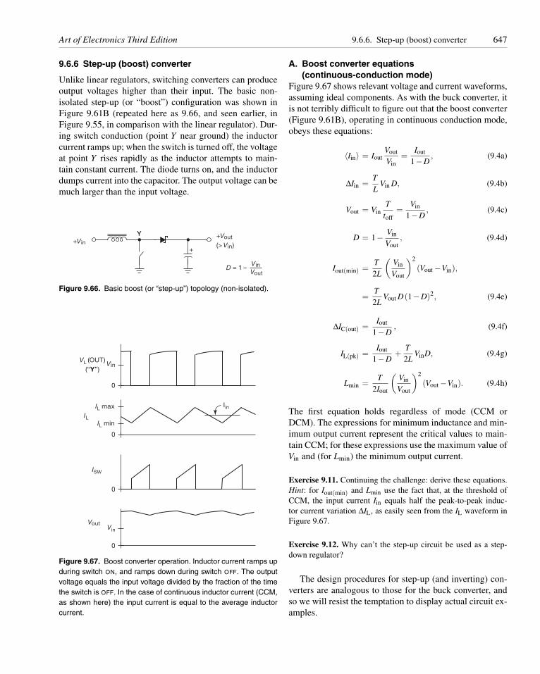
Art of Electronics Third Edition 9.6.6. Step-up (boost) converter 647
9.6.6 Step-up (boost) converter
Unlike linear regulators, switching converters can produceoutput voltages higher than their input. The basic non-isolated step-up (or “boost”) configuration was shown inFigure 9.61B (repeated here as 9.66, and seen earlier, inFigure 9.55, in comparison with the linear regulator). Dur-ing switch conduction (point Y near ground) the inductorcurrent ramps up; when the switch is turned off, the voltageat point Y rises rapidly as the inductor attempts to main-tain constant current. The diode turns on, and the inductordumps current into the capacitor. The output voltage can bemuch larger than the input voltage.
+Vin+Vout
(> Vin)+
Y
D = 1 –Vin
Vout
Figure 9.66. Basic boost (or “step-up”) topology (non-isolated).
VinVL (OUT)
(“Y”)
0
Vin
Vout
0
0
IL max
IL min
IL
Iin
0
ISW
Figure 9.67. Boost converter operation. Inductor current ramps upduring switch ON, and ramps down during switch OFF. The outputvoltage equals the input voltage divided by the fraction of the timethe switch is OFF. In the case of continuous inductor current (CCM,as shown here) the input current is equal to the average inductorcurrent.
A. Boost converter equations(continuous-conduction mode)
Figure 9.67 shows relevant voltage and current waveforms,assuming ideal components. As with the buck converter, itis not terribly difficult to figure out that the boost converter(Figure 9.61B), operating in continuous conduction mode,obeys these equations:
〈Iin〉 = IoutVout
Vin=
Iout
1−D, (9.4a)
ΔIin =TL
Vin D, (9.4b)
Vout = VinT
toff=
Vin
1−D, (9.4c)
D = 1− Vin
Vout, (9.4d)
Iout(min) =T2L
(Vin
Vout
)2
(Vout −Vin),
=T2L
Vout D(1−D)2, (9.4e)
ΔIC(out) =Iout
1−D, (9.4f)
IL(pk) =Iout
1−D+
T2L
VinD, (9.4g)
Lmin =T
2Iout
(Vin
Vout
)2
(Vout −Vin). (9.4h)
The first equation holds regardless of mode (CCM orDCM). The expressions for minimum inductance and min-imum output current represent the critical values to main-tain CCM; for these expressions use the maximum value ofVin and (for Lmin) the minimum output current.
Exercise 9.11. Continuing the challenge: derive these equations.Hint: for Iout(min) and Lmin use the fact that, at the threshold ofCCM, the input current Iin equals half the peak-to-peak induc-tor current variation ΔIL, as easily seen from the IL waveform inFigure 9.67.
Exercise 9.12. Why can’t the step-up circuit be used as a step-down regulator?
The design procedures for step-up (and inverting) con-verters are analogous to those for the buck converter, andso we will resist the temptation to display actual circuit ex-amples.
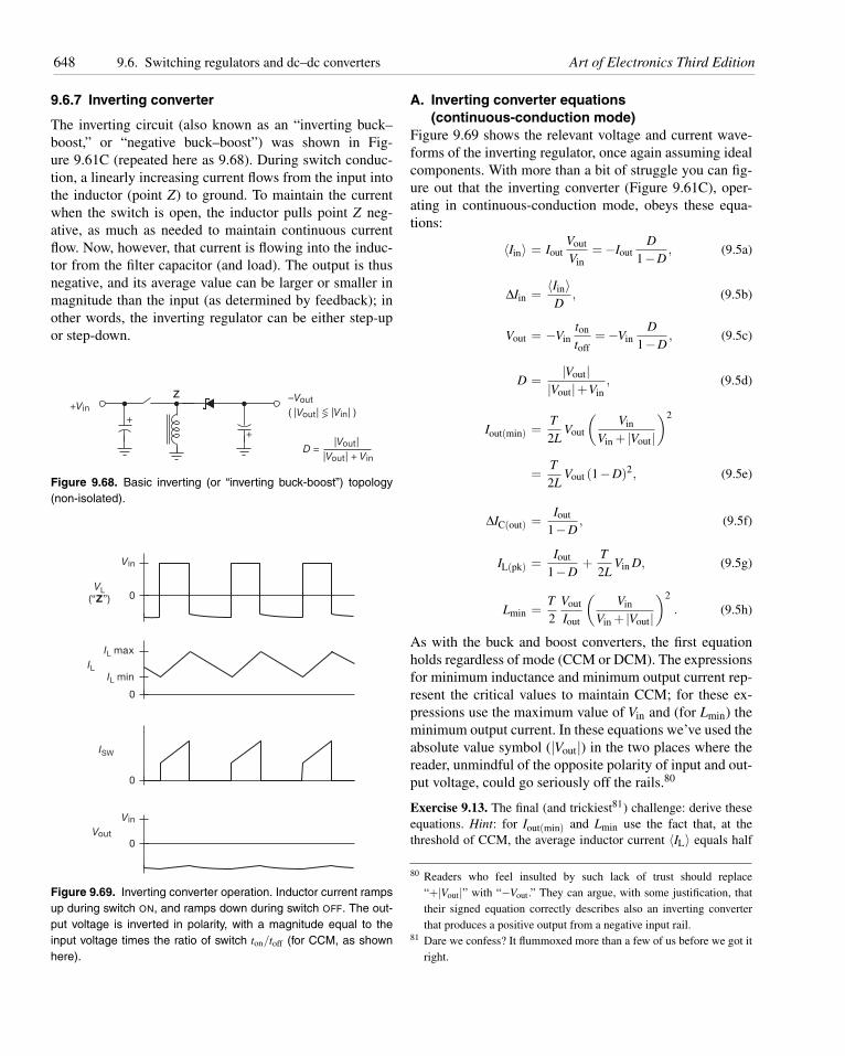
648 9.6. Switching regulators and dc–dc converters Art of Electronics Third Edition
9.6.7 Inverting converter
The inverting circuit (also known as an “inverting buck–boost,” or “negative buck–boost”) was shown in Fig-ure 9.61C (repeated here as 9.68). During switch conduc-tion, a linearly increasing current flows from the input intothe inductor (point Z) to ground. To maintain the currentwhen the switch is open, the inductor pulls point Z neg-ative, as much as needed to maintain continuous currentflow. Now, however, that current is flowing into the induc-tor from the filter capacitor (and load). The output is thusnegative, and its average value can be larger or smaller inmagnitude than the input (as determined by feedback); inother words, the inverting regulator can be either step-upor step-down.
+Vin
+
+
Z –Vout
( |Vout| >< |Vin| )
D =|Vout|
|Vout| + Vin
Figure 9.68. Basic inverting (or “inverting buck-boost”) topology(non-isolated).
Vin
VL
(“Z”) 0
Vin
Vout0
0
IL max
IL min
IL
0
ISW
Figure 9.69. Inverting converter operation. Inductor current rampsup during switch ON, and ramps down during switch OFF. The out-put voltage is inverted in polarity, with a magnitude equal to theinput voltage times the ratio of switch ton/toff (for CCM, as shownhere).
A. Inverting converter equations(continuous-conduction mode)
Figure 9.69 shows the relevant voltage and current wave-forms of the inverting regulator, once again assuming idealcomponents. With more than a bit of struggle you can fig-ure out that the inverting converter (Figure 9.61C), oper-ating in continuous-conduction mode, obeys these equa-tions:
〈Iin〉 = IoutVout
Vin= −Iout
D1−D
, (9.5a)
ΔIin =〈Iin〉
D, (9.5b)
Vout = −Vinton
toff= −Vin
D1−D
, (9.5c)
D =|Vout|
|Vout|+Vin, (9.5d)
Iout(min) =T2L
Vout
(Vin
Vin + |Vout|)2
=T2L
Vout (1−D)2, (9.5e)
ΔIC(out) =Iout
1−D, (9.5f)
IL(pk) =Iout
1−D+
T2L
Vin D, (9.5g)
Lmin =T2
Vout
Iout
(Vin
Vin + |Vout|)2
. (9.5h)
As with the buck and boost converters, the first equationholds regardless of mode (CCM or DCM). The expressionsfor minimum inductance and minimum output current rep-resent the critical values to maintain CCM; for these ex-pressions use the maximum value of Vin and (for Lmin) theminimum output current. In these equations we’ve used theabsolute value symbol (|Vout|) in the two places where thereader, unmindful of the opposite polarity of input and out-put voltage, could go seriously off the rails.80
Exercise 9.13. The final (and trickiest81) challenge: derive theseequations. Hint: for Iout(min) and Lmin use the fact that, at thethreshold of CCM, the average inductor current 〈IL〉 equals half
80 Readers who feel insulted by such lack of trust should replace“+|Vout|” with “−Vout.” They can argue, with some justification, thattheir signed equation correctly describes also an inverting converterthat produces a positive output from a negative input rail.
81 Dare we confess? It flummoxed more than a few of us before we got itright.
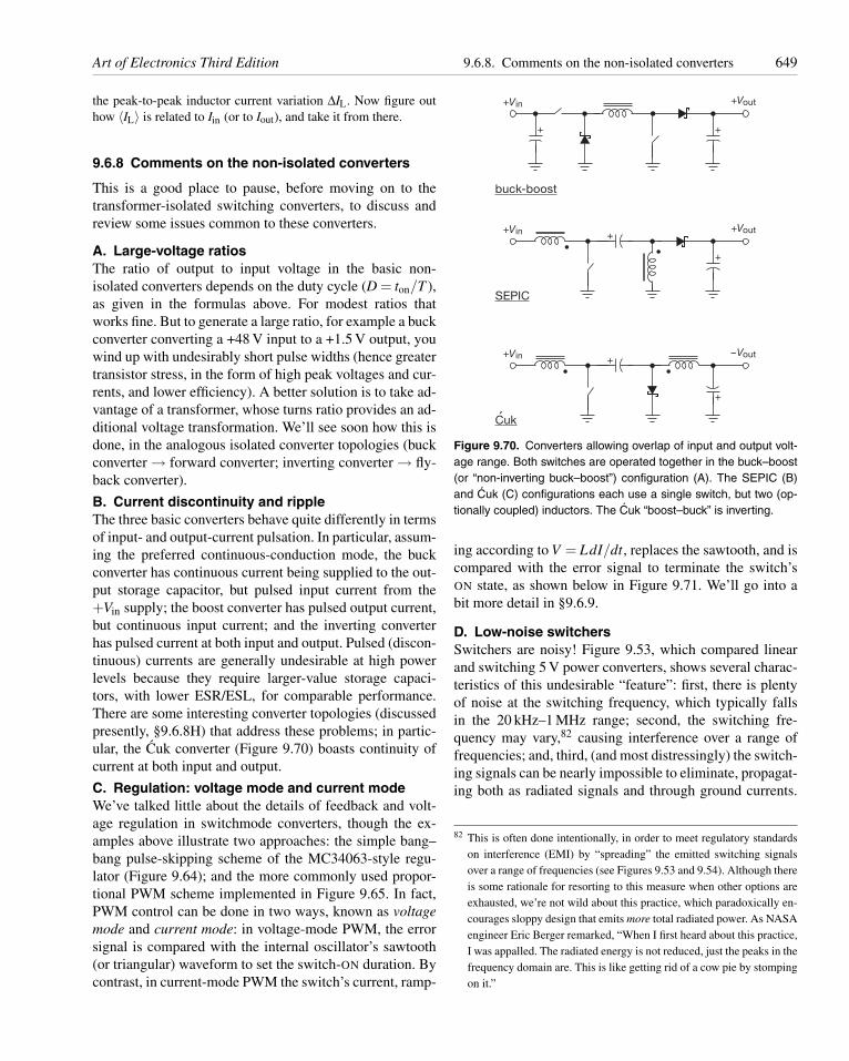
Art of Electronics Third Edition 9.6.8. Comments on the non-isolated converters 649
the peak-to-peak inductor current variation ΔIL. Now figure outhow 〈IL〉 is related to Iin (or to Iout), and take it from there.
9.6.8 Comments on the non-isolated converters
This is a good place to pause, before moving on to thetransformer-isolated switching converters, to discuss andreview some issues common to these converters.
A. Large-voltage ratiosThe ratio of output to input voltage in the basic non-isolated converters depends on the duty cycle (D = ton/T ),as given in the formulas above. For modest ratios thatworks fine. But to generate a large ratio, for example a buckconverter converting a +48 V input to a +1.5 V output, youwind up with undesirably short pulse widths (hence greatertransistor stress, in the form of high peak voltages and cur-rents, and lower efficiency). A better solution is to take ad-vantage of a transformer, whose turns ratio provides an ad-ditional voltage transformation. We’ll see soon how this isdone, in the analogous isolated converter topologies (buckconverter → forward converter; inverting converter → fly-back converter).
B. Current discontinuity and rippleThe three basic converters behave quite differently in termsof input- and output-current pulsation. In particular, assum-ing the preferred continuous-conduction mode, the buckconverter has continuous current being supplied to the out-put storage capacitor, but pulsed input current from the+Vin supply; the boost converter has pulsed output current,but continuous input current; and the inverting converterhas pulsed current at both input and output. Pulsed (discon-tinuous) currents are generally undesirable at high powerlevels because they require larger-value storage capaci-tors, with lower ESR/ESL, for comparable performance.There are some interesting converter topologies (discussedpresently, §9.6.8H) that address these problems; in partic-ular, the Cuk converter (Figure 9.70) boasts continuity ofcurrent at both input and output.
C. Regulation: voltage mode and current modeWe’ve talked little about the details of feedback and volt-age regulation in switchmode converters, though the ex-amples above illustrate two approaches: the simple bang–bang pulse-skipping scheme of the MC34063-style regu-lator (Figure 9.64); and the more commonly used propor-tional PWM scheme implemented in Figure 9.65. In fact,PWM control can be done in two ways, known as voltagemode and current mode: in voltage-mode PWM, the errorsignal is compared with the internal oscillator’s sawtooth(or triangular) waveform to set the switch-ON duration. Bycontrast, in current-mode PWM the switch’s current, ramp-
+Vout
+Vout
+ +
buck-boost
+Vin
+Vin
+
+
SEPIC
–Vout+Vin
+
+
Cuk´
Figure 9.70. Converters allowing overlap of input and output volt-age range. Both switches are operated together in the buck–boost(or “non-inverting buck–boost”) configuration (A). The SEPIC (B)and Cuk (C) configurations each use a single switch, but two (op-tionally coupled) inductors. The Cuk “boost–buck” is inverting.
ing according to V = LdI/dt, replaces the sawtooth, and iscompared with the error signal to terminate the switch’sON state, as shown below in Figure 9.71. We’ll go into abit more detail in §9.6.9.
D. Low-noise switchersSwitchers are noisy! Figure 9.53, which compared linearand switching 5 V power converters, shows several charac-teristics of this undesirable “feature”: first, there is plentyof noise at the switching frequency, which typically fallsin the 20 kHz–1 MHz range; second, the switching fre-quency may vary,82 causing interference over a range offrequencies; and, third, (and most distressingly) the switch-ing signals can be nearly impossible to eliminate, propagat-ing both as radiated signals and through ground currents.
82 This is often done intentionally, in order to meet regulatory standardson interference (EMI) by “spreading” the emitted switching signalsover a range of frequencies (see Figures 9.53 and 9.54). Although thereis some rationale for resorting to this measure when other options areexhausted, we’re not wild about this practice, which paradoxically en-courages sloppy design that emits more total radiated power. As NASAengineer Eric Berger remarked, “When I first heard about this practice,I was appalled. The radiated energy is not reduced, just the peaks in thefrequency domain are. This is like getting rid of a cow pie by stompingon it.”
650 9.6. Switching regulators and dc–dc converters Art of Electronics Third Edition
Figure 9.53 illustrates this latter point well: the switch-ing noise can be heavily bypassed at one point, as in Fig-ure 9.53B; but just put your ’scope probe a few inches away(Figure 9.53C and D) and they’re back!
This problem is widely recognized, and there are vari-ous approaches to cleaning up switcher noise. At a simplelevel, a low-dropout regulator at the output helps consid-erably, as does a simple LC output filter. A more sophis-ticated approach is to use converter topologies that avoidcurrent pulsations at the input and output (for example theCuk converter, §9.6.8H), or that exploit the resonant prop-erties of inductance and capacitance so that the switchesare brought into conduction at moments when the voltageacross them is near zero (“zero-voltage switching,” ZVS),and are opened when the current is near zero (“zero-currentswitching,” ZCS). Finally, some converters (typified by theLT1533, LT1534, LT1738, and LT3439) incorporate cir-cuitry to limit the switching transistor’s voltage and cur-rent slew rates, which reduces both radiated and ground-conducted switching noise.
When thinking about switching converter noise, keep inmind that it emerges in multiple ways, namely:(a) ripple impressed across the dc output terminals, at theswitching frequency, typically of the order of 10–100 mVpeak-to-peak;(b) common-mode ripple on the dc output (which you canthink of as ground-line ripple current), which causes thekind of mischief seen in Figure 9.53C;(c) ripple, again at the switching frequency, impressed ontothe input supply;(d) radiated noise, at the switching frequency and its har-monics, from switched currents in the inductors and leads.
You can get into plenty of trouble with switching sup-plies in a circuit that has low-level signals (say 100 μV orless). Although an aggressive job of shielding and filteringmay solve such problems, you’re probably better off withlinear regulators from the outset.
E. Inductance tradeoffsThere’s some flexibility in the choice of inductance. Usu-ally you want to run PWM converters (but not bang–bang converters like the MC34063 in our first example)in continuous-conduction mode, which sets a minimum in-ductance for a given switching frequency and value of min-imum load current. A larger inductor lowers the minimumload current, reduces the ripple current for a given load cur-rent, and improves the efficiency; but a larger inductor alsoreduces the maximum load current, degrades the transient
response,83 and adds physical size to the converter. It’s atradeoff.
F. Feedback stabilitySwitching converters require considerably more care inthe design of the frequency-compensation network than,say, an op-amp circuit. At least three factors contributeto this: the output LC network produces a “2-pole” lag-ging phase shift (ultimately reaching 180◦), which requiresa compensating “zero”; the load’s characteristics (addi-tional bypass capacitance, nonlinearities, etc.) affect theloop characteristics; and the converter’s gain and phase ver-sus frequency characteristics change abruptly if the con-verter enters discontinuous-conduction mode. And, to adda bit more complexity into an already-complex situation,there are important differences between voltage-mode andcurrent-mode converters: for example, the latter, which arebetter behaved in terms of LC-network phase shifts, exhibita “subharmonic instability” when operated at switch dutycycles greater than 50% (this is addressed by a techniquecalled slope compensation).
The easiest approach for the casual user is to chooseconverters with built-in compensation (for example, theSimple Switcher series, as in Figure 9.65), or convertersthat provide complete recipes for reliable external com-pensation. Regardless, the circuit designer (you!) shouldbe sure to test the stuff you’ve designed.84
G. Soft startWhen input voltage is initially applied to any voltage-regulator circuit, feedback will attempt to bring the out-put to the target voltage. In the case of a switching con-verter, the effect is to command maximum duty cycle fromthe switch, cycle after cycle. This generates a large inrushcurrent (from charging the output capacitor), but, worse, itcan cause the output voltage to overshoot, with potentiallydamaging effects on the load. Worse still, the magnetic coreof the inductor (or transformer) may saturate (reachingmaximum flux density), whereupon the inductance dropsprecipitously, causing the switch current to spike. Core sat-uration is a major cause of component failure; you don’twant it.
These problems are most severe in converters that run
83 Transient speed is a major reason to use low inductance values inswitching converters that power microprocessors, where you see theconcept of critical inductance, i.e., an inductance small enough to han-dle the load step transients.
84 When testing for stability, don’t forget about the negative-resistance in-put characteristic of switching converters; be sure to test with whateverinput filters you plan to use.
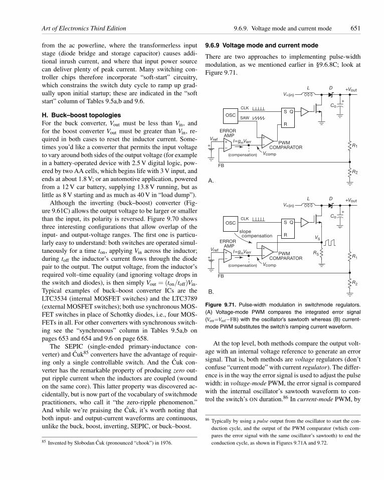
Art of Electronics Third Edition 9.6.9. Voltage mode and current mode 651
from the ac powerline, where the transformerless inputstage (diode bridge and storage capacitor) causes addi-tional inrush current, and where that input power sourcecan deliver plenty of peak current. Many switching con-troller chips therefore incorporate “soft-start” circuitry,which constrains the switch duty cycle to ramp up grad-ually upon initial startup; these are indicated in the “softstart” column of Tables 9.5a,b and 9.6.
H. Buck–boost topologiesFor the buck converter, Vout must be less than Vin, andfor the boost converter Vout must be greater than Vin, re-quired in both cases to reset the inductor current. Some-times you’d like a converter that permits the input voltageto vary around both sides of the output voltage (for examplein a battery-operated device with 2.5 V digital logic, pow-ered by two AA cells, which begins life with 3 V input, andends at about 1.8 V; or an automotive application, poweredfrom a 12 V car battery, supplying 13.8 V running, but aslittle as 8 V starting and as much as 40 V in “load dump”).
Although the inverting (buck–boost) converter (Fig-ure 9.61C) allows the output voltage to be larger or smallerthan the input, its polarity is reversed. Figure 9.70 showsthree interesting configurations that allow overlap of theinput- and output-voltage ranges. The first one is particu-larly easy to understand: both switches are operated simul-taneously for a time ton, applying Vin across the inductor;during toff the inductor’s current flows through the diodepair to the output. The output voltage, from the inductor’srequired volt–time equality (and ignoring voltage drops inthe switch and diodes), is then simply Vout = (ton/toff)Vin.Typical examples of buck–boost converter ICs are theLTC3534 (internal MOSFET switches) and the LTC3789(external MOSFET switches); both use synchronous MOS-FET switches in place of Schottky diodes, i.e., four MOS-FETs in all. For other converters with synchronous switch-ing see the “synchronous” column in Tables 9.5a,b onpages 653 and 654 and 9.6 on page 658.
The SEPIC (single-ended primary-inductance con-verter) and Cuk85 converters have the advantage of requir-ing only a single controllable switch. And the Cuk con-verter has the remarkable property of producing zero out-put ripple current when the inductors are coupled (woundon the same core). This latter property was discovered ac-cidentally, but is now part of the vocabulary of switchmodepractitioners, who call it “the zero-ripple phenomenon.”And while we’re praising the Cuk, it’s worth noting thatboth input- and output-current waveforms are continuous,unlike the buck, boost, inverting, SEPIC, or buck–boost.
85 Invented by Slobodan Cuk (pronounced “chook”) in 1976.
9.6.9 Voltage mode and current mode
There are two approaches to implementing pulse-widthmodulation, as we mentioned earlier in §9.6.8C; look atFigure 9.71.
OSC
CLK
SAW
(compensation)
Vref
OSC
S
R
Q
PWMCOMPARATOR
PWMCOMPARATOR
ERROR AMP
ERROR AMP
FB
++
––
+
–
+
R2
R1
VS
CLK
slopecompensation
A.
B.
Vref
S
R
Q
FB
++
–
I=gmVerr
Vcomp
R2
R1
RS
(compensation)
I=gmVerr
Vcomp
+VoutV+(in)
Co
+
L D
+VoutV+(in)
Co
+
L D
Figure 9.71. Pulse-width modulation in switchmode regulators.(A) Voltage-mode PWM compares the integrated error signal(Verr=Vref−FB) with the oscillator’s sawtooth whereas (B) current-mode PWM substitutes the switch’s ramping current waveform.
At the top level, both methods compare the output volt-age with an internal voltage reference to generate an errorsignal. That is, both methods are voltage regulators (don’tconfuse “current mode” with current regulator). The differ-ence is in the way the error signal is used to adjust the pulsewidth: in voltage-mode PWM, the error signal is comparedwith the internal oscillator’s sawtooth waveform to con-trol the switch’s ON duration.86 In current-mode PWM, by
86 Typically by using a pulse output from the oscillator to start the con-duction cycle, and the output of the PWM comparator (which com-pares the error signal with the same oscillator’s sawtooth) to end theconduction cycle, as shown in Figures 9.71A and 9.72.
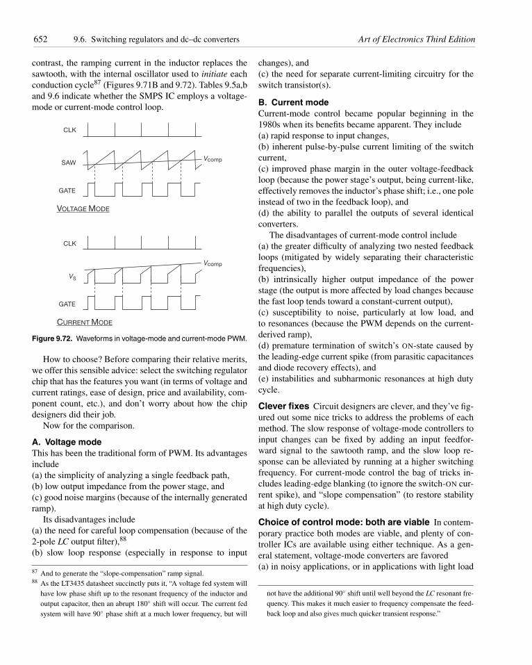
652 9.6. Switching regulators and dc–dc converters Art of Electronics Third Edition
contrast, the ramping current in the inductor replaces thesawtooth, with the internal oscillator used to initiate eachconduction cycle87 (Figures 9.71B and 9.72). Tables 9.5a,band 9.6 indicate whether the SMPS IC employs a voltage-mode or current-mode control loop.
CLK
SAWVcomp
Vcomp
GATE
VOLTAGE MODE
CLK
VS
GATE
CURRENT MODE
Figure 9.72. Waveforms in voltage-mode and current-mode PWM.
How to choose? Before comparing their relative merits,we offer this sensible advice: select the switching regulatorchip that has the features you want (in terms of voltage andcurrent ratings, ease of design, price and availability, com-ponent count, etc.), and don’t worry about how the chipdesigners did their job.
Now for the comparison.
A. Voltage modeThis has been the traditional form of PWM. Its advantagesinclude(a) the simplicity of analyzing a single feedback path,(b) low output impedance from the power stage, and(c) good noise margins (because of the internally generatedramp).
Its disadvantages include(a) the need for careful loop compensation (because of the2-pole LC output filter),88
(b) slow loop response (especially in response to input
87 And to generate the “slope-compensation” ramp signal.88 As the LT3435 datasheet succinctly puts it, “A voltage fed system will
have low phase shift up to the resonant frequency of the inductor andoutput capacitor, then an abrupt 180◦ shift will occur. The current fedsystem will have 90◦ phase shift at a much lower frequency, but will
changes), and(c) the need for separate current-limiting circuitry for theswitch transistor(s).
B. Current modeCurrent-mode control became popular beginning in the1980s when its benefits became apparent. They include(a) rapid response to input changes,(b) inherent pulse-by-pulse current limiting of the switchcurrent,(c) improved phase margin in the outer voltage-feedbackloop (because the power stage’s output, being current-like,effectively removes the inductor’s phase shift; i.e., one poleinstead of two in the feedback loop), and(d) the ability to parallel the outputs of several identicalconverters.
The disadvantages of current-mode control include(a) the greater difficulty of analyzing two nested feedbackloops (mitigated by widely separating their characteristicfrequencies),(b) intrinsically higher output impedance of the powerstage (the output is more affected by load changes becausethe fast loop tends toward a constant-current output),(c) susceptibility to noise, particularly at low load, andto resonances (because the PWM depends on the current-derived ramp),(d) premature termination of switch’s ON-state caused bythe leading-edge current spike (from parasitic capacitancesand diode recovery effects), and(e) instabilities and subharmonic resonances at high dutycycle.
Clever fixes Circuit designers are clever, and they’ve fig-ured out some nice tricks to address the problems of eachmethod. The slow response of voltage-mode controllers toinput changes can be fixed by adding an input feedfor-ward signal to the sawtooth ramp, and the slow loop re-sponse can be alleviated by running at a higher switchingfrequency. For current-mode control the bag of tricks in-cludes leading-edge blanking (to ignore the switch-ON cur-rent spike), and “slope compensation” (to restore stabilityat high duty cycle).
Choice of control mode: both are viable In contem-porary practice both modes are viable, and plenty of con-troller ICs are available using either technique. As a gen-eral statement, voltage-mode converters are favored(a) in noisy applications, or in applications with light load
not have the additional 90◦ shift until well beyond the LC resonant fre-quency. This makes it much easier to frequency compensate the feed-back loop and also gives much quicker transient response.”
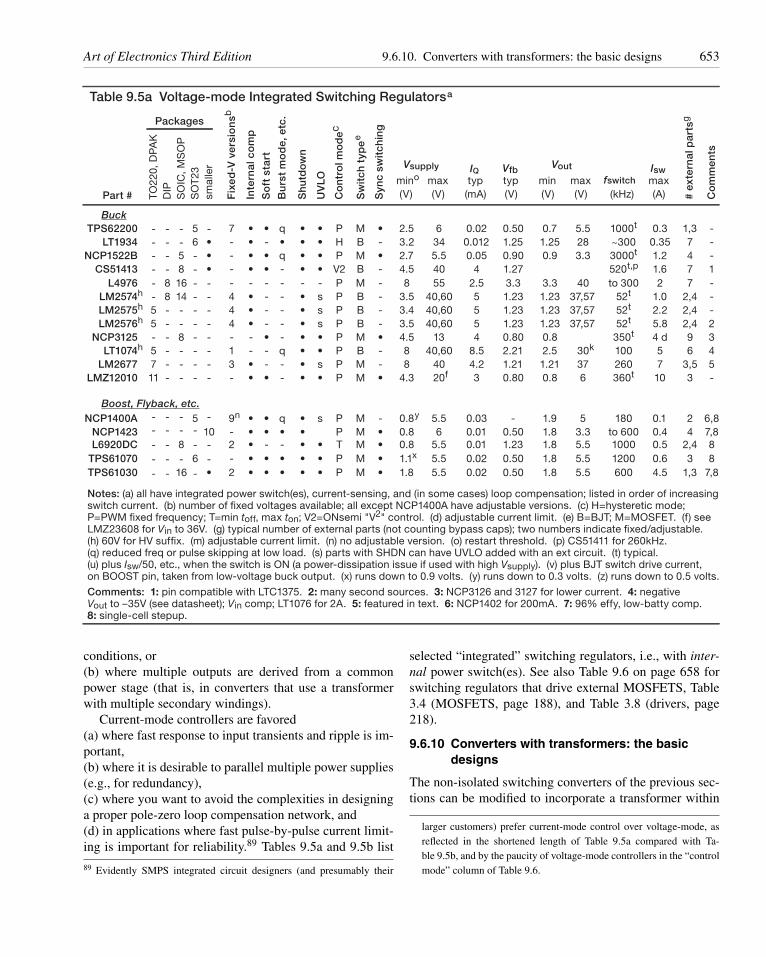
Art of Electronics Third Edition 9.6.10. Converters with transformers: the basic designs 653
Table 9.5a Voltage-mode Integrated Switching Regulatorsa
Part #
Packages
TO22
0, D
PA
KD
IPS
OIC
, MS
OP
SO
T23
smal
ler
Fix
ed
-V v
ers
ion
sb
Inte
rna
l c
om
p
So
ft s
tart
Bu
rst
mo
de
, e
tc.
Sh
utd
ow
n
UV
LO
# e
xte
rna
l p
art
sg
Co
mm
en
ts
Co
ntr
ol m
od
ec
Sw
itc
h t
yp
ee
Syn
c s
wit
ch
ing
Vsupply VoutIQ Vfbfswitch
Isw
mino max typtyp min max max(V) (V) (mA) (V) (V) (V) (kHz) (A)
BuckTPS62200 5 7 • • q • • P M • 2.5 6 0.02 0.50 0.7 5.5 1000t 0.3 1,3
LT1934 6 • - • - • • H B - 3.2 34 0.012 1.25 1.25 28 ~300 0.35 7NCP1522B 5 • - • • q • • P M • 2.7 5.5 0.05 0.90 0.9 3.3 3000t 1.2 4
CS51413 8 • - • • • • V2 B - 4.5 40 4 1.27 520t,p 1.6 7L4976 8 16 - - - -
-- - P M - 8 55 2.5 3.3 3.3 40 to 300 2 7
LM2574h 8 14 4 • - - • s P B - 3.5 40,60 5 1.23 1.23 37,57 52t 1.0 2,4LM2575h 5 4 • - - • s P B - 3.4 40,60 5 1.23 1.23 37,57 52t 2.2 2,4LM2576h 5 4 • - -
-• s P B - 3.5 40,60 5 1.23 1.23 37,57 52t 5.8 2,4
NCP3125 8 - - • • • P M • 4.5 13 4 0.80 0.8 350t 4 d 9LT1074h 5 1 - - q • • P B - 8 40,60 8.5 2.21 2.5 30k 100 5 6
LM2677 7 3 • - - • s P M - 8 40 4.2 1.21 1.21 37 260 7 3,5LMZ12010 11 - • • - • • P M • 4.3 20f 3 0.80 0.8 6 360t 10 3
Boost, Flyback, etc.NCP1400A 5 9n • • q • s P M - 0.8y 5.5 0.03 - 1.9 5 180 0.1 2
NCP1423 10 - • • • • P M • 0.8 6 0.01 0.50 1.8 3.3 to 600 0.4 4
TPS61030 16 • 2 • • • • P M • 1.8 5.5 0.02 0.50 1.8 5.5 600 4.5 1,3
Notes: (a) all have integrated power switch(es), current-sensing, and (in some cases) loop compensation; listed in order of increasingswitch current. (b) number of fixed voltages available; all except NCP1400A have adjustable versions. (c) H=hysteretic mode;P=PWM fixed frequency; T=min toff, max ton; V2=ONsemi "V2" control. (d) adjustable current limit. (e) B=BJT; M=MOSFET. (f) seeLMZ23608 for Vin to 36V. (g) typical number of external parts (not counting bypass caps); two numbers indicate fixed/adjustable.(h) 60V for HV suffix. (m) adjustable current limit. (n) no adjustable version. (o) restart threshold. (p) CS51411 for 260kHz.(q) reduced freq or pulse skipping at low load. (s) parts with SHDN can have UVLO added with an ext circuit. (t) typical.(u) plus Isw/50, etc., when the switch is ON (a power-dissipation issue if used with high Vsupply). (v) plus BJT switch drive current,on BOOST pin, taken from low-voltage buck output. (x) runs down to 0.9 volts. (y) runs down to 0.3 volts. (z) runs down to 0.5 volts.
L6920DC 8 2 • - - • • T M • 0.8 5.5 0.01 1.23 1.8 5.5 1000 0.5 2,4TPS61070 6 - • • • • P M
---1---2345-
6,87,8
7,8
88• 1.1x 5.5 0.02 0.50 1.8 5.5 1200 0.6 3
- ---
-----
--
--
---
--
--
---
--
- ---
--
--
--
- --- ---
----- -
----
-- - --
---
-
-
••
•
Comments: 1: pin compatible with LTC1375. 2: many second sources. 3: NCP3126 and 3127 for lower current. 4: negativeVout to –35V (see datasheet); Vin comp; LT1076 for 2A. 5: featured in text. 6: NCP1402 for 200mA. 7: 96% effy, low-batty comp.8: single-cell stepup.
conditions, or(b) where multiple outputs are derived from a commonpower stage (that is, in converters that use a transformerwith multiple secondary windings).
Current-mode controllers are favored(a) where fast response to input transients and ripple is im-portant,(b) where it is desirable to parallel multiple power supplies(e.g., for redundancy),(c) where you want to avoid the complexities in designinga proper pole-zero loop compensation network, and(d) in applications where fast pulse-by-pulse current limit-ing is important for reliability.89 Tables 9.5a and 9.5b list
89 Evidently SMPS integrated circuit designers (and presumably their
selected “integrated” switching regulators, i.e., with inter-nal power switch(es). See also Table 9.6 on page 658 forswitching regulators that drive external MOSFETS, Table3.4 (MOSFETS, page 188), and Table 3.8 (drivers, page218).
9.6.10 Converters with transformers: the basicdesigns
The non-isolated switching converters of the previous sec-tions can be modified to incorporate a transformer within
larger customers) prefer current-mode control over voltage-mode, asreflected in the shortened length of Table 9.5a compared with Ta-ble 9.5b, and by the paucity of voltage-mode controllers in the “controlmode” column of Table 9.6.
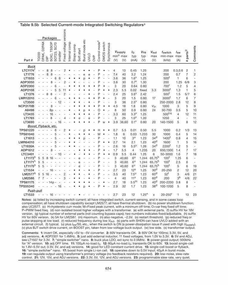
p
NCP3170B - - - 8 - - - - • • • • • P • • 4.5 18 1.8 Vin0.80 1000 3 5
A8498 - - - 8p - - - • - • p • - O • - 8 50 0.9 0.80 24 30-700 3.5 5
LT3435 - - - 16 - - - - • • • • - P - - 3.3 60 3.3v 1.25 500t,q 4 12
LT3690 - - - - - 16 - - • • • • - P w • 3.9 36,60 0.1v 0.80 20 140-1500 5 8
Boost, Flyback, etc.TPS61220 - - - - 6 - 2 • - - p • • H • • 0.7 5.5 0.01 0.50 5.5 1000 0.2 1/3
TPS61040 - - - - 5 - - • - • • • - M • - 1.8 6 0.03 1.233 30 1000 0.4 5
LT1613 - - - - 5 - - • • • p - - P - - 1.1 10 3u 1.23 34d 1400t 0.8 4
LMR64010 - - - - 5 - - • • - - - - P • • 2.7 14 2.1 1.23 40d 1600 1 5
LT1930A - - - - 5 - - • • - - - - P - - 2.6 16 5.5u 1.26 34d 2200t 1.2 5
LT1172h 5 5 8 16 - - - - - e - - - P - - 3 40,60 6u 1.244 65,75h 100t 1.25 6
LT1171h 5 5 - - - - - - - e - - - P - - 3 40,60 6u 1.244 65,75h 100t 2.5 6
LT1170h 5 5 - - - - - - - e - - - P - - 3 40,60 6u 1.244 65,75h 100t 5 6
LT1534 - - - 16 - - - - • • - • - P - - 2.7 23 12u 1.25 30d 20-250 2 12
LM2577b 5 5 16 - - - 2 - • • - • - P - - 3.5 40 7.5u
1.7
1.23 60d 52t 3 4/6
LM2586 7 7 - - - - 3 - • • - • - P - - 4 40 11u 1.23 60d 200 3k 4/6
TPS61175 - - - 14 - - - - • • • • - - • - 2.7 18 3.5m 1.23 40d 200-2200 3.8 8
TPS55340 - - - - - 16 - - • • p • - P • - 2.9 32 1.23 38d 100-1200 5 8
9
10
11
12
13
14
15
16
-
-
-
19
20
21
22
-
-
Notes: (a) listed by increasing switch current; all have integrated switch, current-sensing, and in some cases loopcompensation; all have shutdown capability except LM2577; all have thermal shutdown. (b) no power shutdown function;also UC2577. (c) H=hysteretic curr mode; M=Fixed peak current, with a minimum off time; O=var freq fixed off time;P=PWM fixed freq. (d) non-isolated boost higher voltages with a transformer. (e) with external parts. (f) suffix HV for 18Vversion. (g) typical number of external parts (not counting bypass caps); two numbers indicates fixed/adjustable. (h) suffixHV for 60V version. (k) 5A for LM2587. (m) maximum. (n) also negative, –2.5V. (o) restart threshold. (p) reduced freq orpulse skipping at low load. (r) reduced frequency during low Vout. (s) parts with SHDN can have UVLO added with anexternal circuit. (t) typical. (u) plus Isw/50, etc., when the switch is ON (a power-dissipation issue if used with high Vsupply).(v) plus BJT switch drive current, on BOOST pin, taken from low-voltage buck output. (w) low side. (x) transformer output.
ADP3050 - - - 8 - - 2 - • - - - - P - - 3.6 30 0.7v 1.30 200 1.25 36/8
ADP2300 - - - - 6 - - • • • • • • P • - 3 20 0.64 0.80 700r 1.2 45
ADP2108 - - - - 5 5 11 • - • • • - P • • 2.3 5.5 0.02 fixed 3.3 3000t 1.3 1
LT1376 - - 8 8 - - 2 - - - - • - P - - 2.4 25 3.6v 2.42 500t 1.5 5/7
LMR12010 - - - - 6 - - • • • - • • P • - 3 20 1.5 0.80 17 3000t 1.7 6
LT3500 - - - - - 12 - - • • - • - P - - 3 36 2.5v 0.80 250-2000 2.8 12
5
6
7
8
Table 9.5b Selected Current-mode Integrated Switching Regulatorsa
Part #
PackagesT
O2
20
DP
AK
, D
2P
AK
DIP
SO
IC,
TS
SO
P
SO
T23,
SC
70
sm
alle
r
Fix
ed
-vo
ltag
e v
ers
ion
s
Inte
rnal co
mp
Slo
pe c
om
p
So
ft s
tart
Bu
rst
mo
de e
tc
UV
LO
OV
P
Co
ntr
ol m
od
ec
DM
OS
sw
itch
Syn
ch
ron
ou
s
Vsupply IQ VFB Vout fswitch Isw
# p
art
sg
Co
mm
en
ts
mino max typ typ max min-max max
(V) (V) (mA) (V) (V) (kHz) (A)
BuckLTC1174f - - 8 8 - - 2 • - - • • - P • - 4 13 0.45 1.25 200 0.3,0.6 12
LT1776 - - 8 8 - - - - - - e e - P - - 7.4 40 3.2 1.24 200 0.7 27
LT1933 - - - - 6 6 - • • • p • - P - - 3.6 36 1.6v 1.25 500t 1 -6
LT1765 - - - 8 - - 4 - • e - e - P - - 3 25 1.0v 1.20 1250 4 - 11
ADP1612 - - - 8 - - - - - • • • - P • - 1.7 5.5 4 1.235 20 650,1300 1.4 7 17
Push-pullLT1533 - - - 16 - - - - - • - - - - - - 2.7 23 12 1.25n x 20-250r 1 13 23
LTC3401 - - - - - 10 - - • - • • - P • • 0.9 5.5 0.44 1.25 6 50-3000 1.6 7 18
Comments: 1: invert OK, especially +5V to –5V converter. 2: 60V transients OK. 3: 60V OK for 100ms; 3.3V, 5V, andadj versions. 4: ADP2301 for 1.4MHz. 5: just add external inductor; 11 fixed voltages, from 1.0V to 3.3V. 6: 5V and ADJ,see LT1507 for 3.3V. 7: “simple switcher” nano. 8: buck plus LDO, ext sync to 2.5MHz. 9: power-good output; 500kHzfor “A” version. 10: adj OFF time. 11: 100μA no-load IQ. 12: 80μA no-load IQ; transients OK to 60V. 13: boost single-cellto 1.8V–5.5V out; 3.3V, 5V, and adj versions. 14: good for LED constant current drive. 15: single-cell boost or flyback.16: “simple switcher” nano. 17: boost from single Li-ion cell. 18: operates down to 0.5V input; 40μA in burst mode.19: can regulate output using transformer’s primary voltage (no feedback resistors required). 20: low-noise, slew-ratecontrol. 21: 12V, 15V, and ADJ versions. 22: 3.3V, 5V, 12V, and ADJ versions. 23: programmable slew rate, very quiet.
654
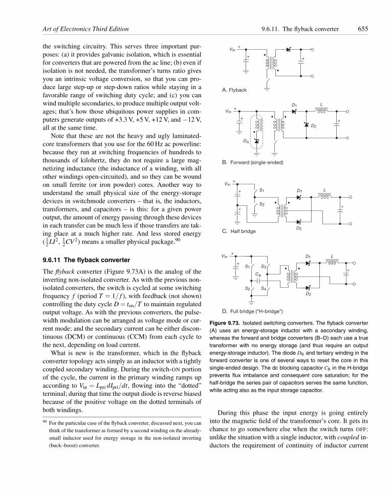
Art of Electronics Third Edition 9.6.11. The flyback converter 655
the switching circuitry. This serves three important pur-poses: (a) it provides galvanic isolation, which is essentialfor converters that are powered from the ac line; (b) even ifisolation is not needed, the transformer’s turns ratio givesyou an intrinsic voltage conversion, so that you can pro-duce large step-up or step-down ratios while staying in afavorable range of switching duty cycle; and (c) you canwind multiple secondaries, to produce multiple output volt-ages; that’s how those ubiquitous power supplies in com-puters generate outputs of +3.3 V, +5 V, +12 V, and −12 V,all at the same time.
Note that these are not the heavy and ugly laminated-core transformers that you use for the 60 Hz ac powerline:because they run at switching frequencies of hundreds tothousands of kilohertz, they do not require a large mag-netizing inductance (the inductance of a winding, with allother windings open-circuited), and so they can be woundon small ferrite (or iron powder) cores. Another way tounderstand the small physical size of the energy-storagedevices in switchmode converters – that is, the inductors,transformers, and capacitors – is this: for a given poweroutput, the amount of energy passing through these devicesin each transfer can be much less if those transfers are tak-ing place at a much higher rate. And less stored energy( 1
2 LI2, 12CV 2) means a smaller physical package.90
9.6.11 The flyback converter
The flyback converter (Figure 9.73A) is the analog of theinverting non-isolated converter. As with the previous non-isolated converters, the switch is cycled at some switchingfrequency f (period T = 1/ f ), with feedback (not shown)controlling the duty cycle D = ton/T to maintain regulatedoutput voltage. As with the previous converters, the pulse-width modulation can be arranged as voltage mode or cur-rent mode; and the secondary current can be either discon-tinuous (DCM) or continuous (CCM) from each cycle tothe next, depending on load current.
What is new is the transformer, which in the flybackconverter topology acts simply as an inductor with a tightlycoupled secondary winding. During the switch-ON portionof the cycle, the current in the primary winding ramps upaccording to Vin = Lpri dIpri/dt, flowing into the “dotted”terminal; during that time the output diode is reverse biasedbecause of the positive voltage on the dotted terminals ofboth windings.
90 For the particular case of the flyback converter, discussed next, you canthink of the transformer as formed by a second winding on the already-small inductor used for energy storage in the non-isolated inverting(buck–boost) converter.
+
A. Flyback
Vin
+
+
B. Forward (single-ended)
C. Half bridge
D. Full bridge (“H-bridge”)
DR
D2
S1
S1
S2
S3
CB
S4
S2
D1
D1
D2
D2
D1 L
+
L
L
+
++
+
+
+
Vin+
Vin+
Vin+
Figure 9.73. Isolated switching converters. The flyback converter(A) uses an energy-storage inductor with a secondary winding,whereas the forward and bridge converters (B–D) each use a truetransformer with no energy storage (and thus require an outputenergy-storage inductor). The diode DR and tertiary winding in theforward converter is one of several ways to reset the core in thissingle-ended design. The dc blocking capacitor CB in the H-bridgeprevents flux imbalance and consequent core saturation; for thehalf-bridge the series pair of capacitors serves the same function,while acting also as the input storage capacitor.
During this phase the input energy is going entirelyinto the magnetic field of the transformer’s core. It gets itschance to go somewhere else when the switch turns OFF:unlike the situation with a single inductor, with coupled in-ductors the requirement of continuity of inductor current
656 9.6. Switching regulators and dc–dc converters Art of Electronics Third Edition
is satisfied if the current continues to flow in any of thewindings. In this case the switch-ON current, flowing intothe dotted terminal, transfers itself to a similarly directedcurrent in the secondary, but multiplied by the turns ratioN≡Npri/Nsec. That current flows to the output (and storagecapacitor), ramping down according to Vout = Lsec dIsec/dt.From equality of inductor volt-seconds, the output voltageis simply
Vout = VinNsec
Npri
ton
toff= Vin
Nsec
Npri
D1−D
(in CCM). (9.6)
And, as usual, efficiency is high, so power is (approxi-mately) conserved:
Iin = IoutVout
Vin. (9.7)
You can wind additional secondaries, each with itsdiode and storage capacitor, to create multiple output volt-ages (as set by the turns ratios). And, because the outputwindings are isolated, you can as easily generate negativeoutputs. Having chosen one of the outputs for regulatingfeedback, however, the others will not be as tightly regu-lated. The term “cross regulation” is used to specify theoutput-voltage dependencies.
A. Comments on flyback converters
Power level Flyback converters have full pulsations ofinput and output current. For this reason they are gener-ally used for low- to medium-power applications (up to∼200 W). For higher power you usually see designs us-ing the forward converter, or, for really high power, bridgeconverters.
The transformer is an inductor The input energy eachcycle is first stored in the transformer core (during switch-ON), then transferred to the output (during the switch-OFF).So the transformer design must provide the correct “mag-netizing inductance” (acting as an inductor), as well as thecorrect turns ratio (acting as a transformer). This is quitedifferent from the situation with the forward converter andthe bridge converters, below, where the transformer is “justa transformer.” We won’t go into further detail about trans-former design here, simply noting that the design of the“magnetics” is an important part of switching converterdesigns in general, and flybacks in particular. You haveto worry about issues such as core cross-section, perme-ability, saturation, and deliberate “gapping” (in general,energy-storage inductors are gapped, whereas pure trans-formers are not). Extremely helpful resources for designare found in IC datasheets and design software (usuallyavailable at no charge from the manufacturer) that provide
specifics about the choice of magnetics. We explore thisimportant topic further in §9x.4.
Snubbers With ideal components, the primary cur-rent would transfer completely to the secondary when theswitch turns OFF, and you wouldn’t have to worry aboutbad things happening on the dangling drain terminal of theswitch. In reality the incomplete coupling between primaryand secondary creates a series “leakage inductance,” whosecraving for current continuity generates a positive voltagespike at the switch, even though the secondary is clampedby the load. This is not good. The usual cure is to includea snubber network, consisting of an RC across the wind-ing, or, better, a “DRC” network of a diode in series with aparallel RC.91
Regulation Flyback converters can be regulated withconventional PWM, either voltage mode or current mode,with a free-running oscillator calling the shots. Alterna-tively, you will see inexpensive designs in which the trans-former itself becomes part of a blocking oscillator, therebysaving a few components. We cracked open some samplesof low-power (5–15 W) “wall warts” and found, well, justabout nothing inside! We reverse engineered them to lookat the circuit tricks (Figure 9.74). They seem to work justfine.
Off-line converters This final circuit (Figure 9.74) is anexample of a power converter that requires galvanic isola-tion. The transformer provides isolation for the power flow;in addition, the feedback signal from the dc output mustbe isolated as well on its way back to the primary side.This can be done with an optocoupler, as here, or withan additional small pulse transformer. We discuss theseoffline converters briefly in §9.7, and in Chapter 9x wediscuss high-efficiency (“green”) power supplies, includ-ing a graph comparing the performance of this 5 W supply(whose standby power is 200 mW) with others.
9.6.12 Forward converters
The single-ended forward converter (Figure 9.73B) isthe transformer-isolated version of the buck converter. Itis helpful to refer back to the basic buck circuit (Fig-ure 9.61A), to see how it goes. The transformer converts
91 Leakage inductance values are typically ∼1% of the magnetizing in-ductance. You can reduce leakage inductance greatly by splitting oneof the windings (say primary) into two, with the other (secondary)sandwiched in between. And bifilar windings (wind primary and sec-ondary as a pair of wires together) can reduce the leakage inductance toa low value. However these techniques increase inter-winding capaci-tance, and bifilar windings suffer from poor voltage insulation ratings.
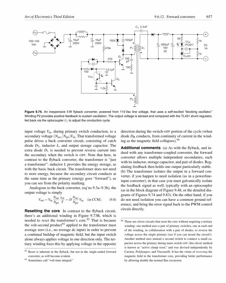
Art of Electronics Third Edition 9.6.12. Forward converters 657
100–140
Vac
150
270
470k
150V 100pF
100pF
100
P1
Q1
Q2
P2
S1
U1b
+ +10μF
200V680μF
10V
(2)
TL431
39
CY 2.2nF
U1a
PC817
1k
1k
1.2k
5V,
1A
+
0.1μF
10μF
200V
–
+ +
Figure 9.74. An inexpensive 5 W flyback converter, powered from 115 Vac line voltage, that uses a self-excited “blocking oscillator.”Winding P2 provides positive feedback to sustain oscillation. The output voltage is sensed and compared with the TL431 shunt regulator,fed back via the optocoupler U1 to adjust the conduction cycle.
input voltage Vin, during primary switch conduction, to asecondary voltage (Nsec/Npri)Vin. That transformed voltagepulse drives a buck converter circuit, consisting of catchdiode D2, inductor L, and output storage capacitor. Theextra diode D1 is needed to prevent reverse current intothe secondary when the switch is OFF. Note that here, incontrast to the flyback converter, the transformer is “justa transformer”: inductor L provides the energy storage, aswith the basic buck circuit. The transformer does not needto store energy, because the secondary circuit conducts atthe same time as the primary (energy goes “forward”), asyou can see from the polarity marking.
Analogous to the buck converter, (eq’ns 9.3a–9.3h), theoutput voltage is simply
Vout = VinNsec
Npri
ton
T= D
Nsec
NpriVin (in CCM). (9.8)
Resetting the core In contrast to the flyback circuit,there’s an additional winding in Figure 9.73B, which isneeded to reset the transformer’s core.92 That is becausethe volt-second product93 applied to the transformer mustaverage zero (i.e., no average dc input) in order to preventa continual buildup of magnetic field; but the input switchalone always applies voltage in one direction only. The ter-tiary winding fixes this by applying voltage in the opposite
92 Reset is inherent in the flyback, but not in the single-ended forwardconverter, as will become evident.
93 Sometimes call “volt-time integral.”
direction during the switch-OFF portion of the cycle (whendiode DR conducts, from continuity of current in the wind-ing as the magnetic field collapses).94
Additional comments (a) As with the flyback, and in-deed with any transformer-coupled converter, the forwardconverter allows multiple independent secondaries, eachwith its inductor, storage capacitor, and pair of diodes. Reg-ulating feedback then holds one output particularly stable.(b) The transformer isolates the output in a forward con-verter, if you happen to need isolation (as in a powerline-input converter); in that case you must galvanically isolatethe feedback signal as well, typically with an optocoupler(as in the block diagram of Figure 9.48, or the detailed dia-grams of Figures 9.74 and 9.83). On the other hand, if youdo not need isolation you can have a common ground ref-erence, and bring the error signal back to the PWM controlcircuit directly.
94 There are clever circuits that reset the core without requiring a tertiarywinding: one method uses a pair of primary switches, one at each endof the winding, in collaboration with a pair of diodes, to reverse thevoltage across the single primary (see if you can invent the circuit!).Another method uses instead a second switch to connect a small ca-pacitor across the primary during main switch-OFF; this clever methodis known as “active clamp reset,” and was devised independently byCarsten, Polykarpov, and Vinciarelli. It has the virtue of reversing themagnetic field in the transformer core, providing better performanceby allowing double the normal flux excursion.
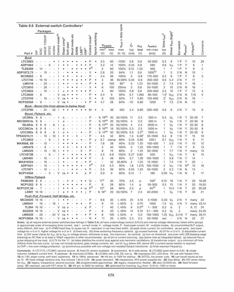
Table 9.6 External-switch Controllersa
Part #
Packages
DIP
SO
IC
MS
OP,
T/S
SO
P
SO
T23
sm
alle
r
Co
ntr
ol m
od
ea
a
Slo
pe c
om
ps
So
ft s
tart
Bu
rst
mo
de
etc
SH
DN
LE
Bo
o
OV
Px
Vo
ut
or
du
ty c
yc
le
Syn
ch
sw
itc
hin
g
Co
ntr
ol m
od
ec
Vsupply VFB
Vref
fswitch Dri
ve I o
utd
Dri
ve
r V
ou
t (h
igh
)k
Ex
t sw
itc
h
Rse
nse?
Co
mm
en
ts
# P
art
sp
p
mino max max typ min-max typ
(V) (V) (V, %) (mA) (V) (kHz) (A)
Buck
ADP1864 - - - 6 - I • • - • • • P -
-
3.2 14 0.24 0.8 580 0.6 Vin 1 P Y 9
TLE6389 - 14 - - - I • - • • • • Pq
5 60 0.12 1.25 360 1 7 1 P Y 9
ADP1872,73 - - 10 - - I - • • • - - V • 2.8 20 1.1 0.6 1000f3 1 5 2 N N 10
NCV8852 - 8 - - I • • - • • - P - 3.4 36 3 0.8 170-500 0.2 8 1 P Y 9
LTC1735 - 16 16 - - I • • • e • • P • 4 36 0.80.45 200-550 0.6 5.2 2 N Y 17
LM5116 - - 20 - - I • • - • • - P • 5 100 5 1.22 50-1000 2 7.4 2 N Y 18
LTC3810 - - 28 - - I - • • • - -
- -
- -
V • 6 100 3 0.8 50-1000 2 10 2 N N 16
LTC3824 - - 10 - - I x • • • • • P - 4 60 0.8 0.8 200-600 2.5 10 1 P Y 13
LTC3830 - 8 - - V na • • • P • 2.4 9 0.7 Vcc1.265 80-550 1.5i 2 N N 7,10
LTC3703 - - 16 - - V na • • • P • 9 100 1.7 0.80 100-600 2i Vcc 2 N N 16
NCP3030A - 8 - - - V na • - - - • P • 4.7 7.528
100%
100%
84%
100%
6V,99%
80u
250ns
100%
90%
93%
84%
30V
0.80~10 1200 1i 2 N N 13
Buck - Boost (Vin from above to below Vout) LTC3780 24 32 I • • • • • • M • 4 36 2.4 0.80 200-400 0.6 6 4 N Y 13
Boost, Flyback, etc.UC384x 8 8 - - - I e - - - - - P - 9, 18ex 30 11 2.5 500 m 0.5 Vc
IQv
1 N Y 20-30
MIC38HC4x 8 8 - - - I e - - - - - P - 9, 16ex 20 4 2.5 500 m 1 Vc 1 N Y 20-30
ISL684x 8 8 8 - 8 I e - - - - - P - 9, 15ex 20 4 2.5 2000 m 1 Vc 1 N Y 20-30
UCC38C4x 8 8 8 - - I e - - - - - P - 9, 16ex 18 2.3 2.5 1000 m 1 Vc 1 N Y 20-30
UCC380x 8 8 8 - 8 I e • - - • - P - 5, 14ex 30 0.5 2.5h 1000 m 1 Vc 1 N Y 20-30
TPS40210,11 - - 10 - 10 I • • - • - - P - 4.5 52 1.5 0.26r 35-1000 0.4 8 1 N Y 15
LTC3803 - - - 6 - I • • - - • - P y 8.7 clamp 0.24 0.80 200 t 0.7 1 N Y 8
MAX668, 69 - - 10 - - I • • • • - - P - 1.8 28 0.22 1.25 100-500 1 5.0 1 N Y 10
LM3478 - - 8 - - I • • - • • • P - 3 40 3 1.25 100-1000 1 7 1 N Y 9
LM5020 - - 10 - 10 I • • - - V - P - 8 15 2 1.25 50-1000 1 7.7 1 N Y many
LTC1872B - - - 6 - I • - • • • • P - 2.5 9.8 0.27 0.80 550 1 Vin 1 N Y 8
LM3481 - - 10 - - I • • • • • • P - 3 48 3.7 1.28 100-1000 1 5.8 1 N Y 14
MAX15004 - - 16 - - I • - - • - • P - - 40 2 1.23 15-1000 1 7.4 1 N Y 20
ADP1621 - - 10 - - I • • • • • - 2.9 5.5 1.8 1.215 100-1500 2 1 N Nw 10
LTC1871 - - 10 - - I - - • • - • P - 2.5 36 0.55 1.23 50-1000 2 5.2 1 N N 13
- - -
NCP1450A - - - 5 - V na • • • e P - 0.9 6 0.14 f 180 0.05 Vin
Vin
1 N N 3
Offline FlybackFAN6300 8 8 - - - I - • • - • • Q - 17o 25 4.5 p 100z 0.15 18 1 N Y 20
NCP1252 8 8 - - - I • • • • • - P - 8 28 1.4 p 50-500 0.5 15 1 N Y 20
NCP1237,38 - 7 - - - I • • • - • w 13o 28 2.5 p 65f3 1 13.5 1 N Y 20
L5991 16 16 - - - I e • • • • j P - 9, 16o 20 7 2.5 40-2000 1 Vc 1 N Y 30
Push-Pull, Forward, Half-Bridge, etc.MC34025 16 16 - - - I • • - - - - P - 9.6 30 25 5.10 5-1000 0.33 Vc 2 N Y many
LM5041 - 16 - - 16 I - • - • • - P - 9 15 3 0.75 1000 1.5 Vc 4 N Y many
TL594 16 16 - - - V na e - - e P - 7 40 9 5.0w 1 - 300 0.2 b 2 - 9, 12
SG3525 16 16 - - - V na • - - - P - 8 40 14 5.10 0.1 - 400 0.2 Vc 2
LM5035 - 20 - - 24 V na • - • • P • 8 105 4 5.0
• • • - R • 11 20
50,100%
50,100%
50,100%
50,100%
50,100%
80%
80%
90%
100%
80%
100%
85%
50,80%
95%
92%
80%
70%
80%
80%
50,100%
t, 45%
t, 50%
t, 45%
t, 49%
t, 50%
t, 50% 2.3 2.5
100-1000 1.25 Vcc
Vcc
2,4 N Y many
many
NCP1395A 16 16 - -
-
-
-
-- V
1
2
-
3
-
-
-
4
5
-
-
6
7
8
8
8
9
10
11
12
13
14
15
-
-
16
-
17
18,28
19,20
20,28
21
22
23,14
24
24,25
26,14
27na 50-1000 ext - 2 N N 22
Notes: (a) all require external power switches (see listings in Table 3.4); all have undervoltage lockout (UVLO) and internal voltage references; listed within groups
in approximate order of increasing drive current. (aa) I - current mode, V - voltage mode, P - fixed peak current, M - multiple modes. (b) uncommitted BJT output,
sinks 200mA, 40V max. (c) P=PWM fixed freq; Q=quasi-res; R - resonant; V=var freq fixed width; (d) peak driver current, for controllers. (e) ext parts. (ex) lower
voltage for x=3 or 5, higher voltage for x=2 or 4. (f) fixed only. (f3) three switching-frequency options. (g) unused footnote. (h) 2V for x=3 or 5. (i) adjustable current
limit. (j) 25V zener clamp for Vcc. (k) to Vcc or voltage shown, whichever is less. (m) maximum. (n) nominal. (o) turn-on threshold. (oo) even with LEB (leading-edge
blanking) an RC filter or at least a 100pF capacitor is often recommended. (p) ref pin is current-sourcing. (pp) [same note as integrated tables]. (q) reduced freq or
pulse skipping at low load. (r) 0.7V for the '11. (s) helps stabilize the control loop against sub-harmonic oscillations. (t) transformer output. (u) a minimum off time
(450ns) limits the duty cycle. (v) may not include dynamic gate-charge currents, etc. (w) for Vout below 30V, above 30V a current-sense resistor is required.
(x) OVP = line over-voltage protection. (y) synchronous possible with low-voltage non-isolated flyback transfomer. (z) finds resonant frequency.
Comments: 1: LTC1772, LTC3801 second-source. 2: fixed 5V version available. 3: automotive. 4: hi-side sense. 5: LTC3832 goes down to 0.6V. 6: single
inductor, foldback current limit. 7: jellybean. 8: improved UC384x. 9: UC384x with LEB, SS, low IQ. 10: impressive 52V, LED drive. 11: use with flyback xfmr.
12: to 1.8V, slope-comp, soft-start, expensive. 13: to 1MHz, advanced. 14: HV pin, to 100V for startup. 15: SOT23, low power, cute. 16: can boost inputs as low
as 1V. 17: fixed voltage versions only, five choices 1.9V to 5.0V. 18: quasi-resonant. 19: inexpensive, ATX power supplies etc. 20: freq dither. 21: 25V zener clamp
for Vcc. 22: legacy, inexpensive, second sourced. 23: programmable gap/overlap. 24: legacy, inexpensive, flexible. 25: also UC3525 etc. 26: feed-forward
ramp. 27: resonant, use with FET driver IC. 28: HV pin, to 500V for startup. 29: optimized for inverting, Vout from –0.4V to –150V or more.
-Pq
-Pq
LTC3863 - - - - • I • • • • - • P • 3.5 60 0.8 0.8 50-850 0.5 8 1 P Y 10–150V 29
658
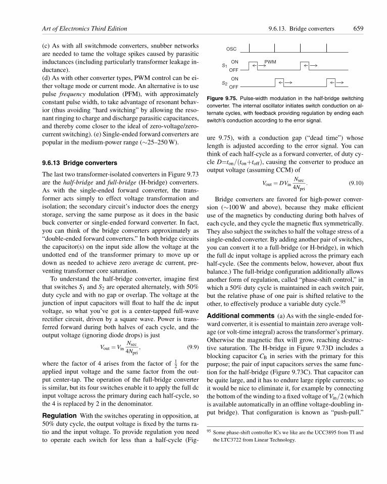
Art of Electronics Third Edition 9.6.13. Bridge converters 659
(c) As with all switchmode converters, snubber networksare needed to tame the voltage spikes caused by parasiticinductances (including particularly transformer leakage in-ductance).(d) As with other converter types, PWM control can be ei-ther voltage mode or current mode. An alternative is to usepulse frequency modulation (PFM), with approximatelyconstant pulse width, to take advantage of resonant behav-ior (thus avoiding “hard switching” by allowing the reso-nant ringing to charge and discharge parasitic capacitances,and thereby come closer to the ideal of zero-voltage/zero-current switching). (e) Single-ended forward converters arepopular in the medium-power range (∼25–250 W).
9.6.13 Bridge converters
The last two transformer-isolated converters in Figure 9.73are the half-bridge and full-bridge (H-bridge) converters.As with the single-ended forward converter, the trans-former acts simply to effect voltage transformation andisolation; the secondary circuit’s inductor does the energystorage, serving the same purpose as it does in the basicbuck converter or single-ended forward converter. In fact,you can think of the bridge converters approximately as“double-ended forward converters.” In both bridge circuitsthe capacitor(s) on the input side allow the voltage at theundotted end of the transformer primary to move up ordown as needed to achieve zero average dc current, pre-venting transformer core saturation.
To understand the half-bridge converter, imagine firstthat switches S1 and S2 are operated alternately, with 50%duty cycle and with no gap or overlap. The voltage at thejunction of input capacitors will float to half the dc inputvoltage, so what you’ve got is a center-tapped full-waverectifier circuit, driven by a square wave. Power is trans-ferred forward during both halves of each cycle, and theoutput voltage (ignoring diode drops) is just
Vout = VinNsec
4Npri, (9.9)
where the factor of 4 arises from the factor of 12 for the
applied input voltage and the same factor from the out-put center-tap. The operation of the full-bridge converteris similar, but its four switches enable it to apply the full dcinput voltage across the primary during each half-cycle, sothe 4 is replaced by 2 in the denominator.
Regulation With the switches operating in opposition, at50% duty cycle, the output voltage is fixed by the turns ra-tio and the input voltage. To provide regulation you needto operate each switch for less than a half-cycle (Fig-
OSC
ON PWM
OFFS1
ON
OFFS2
Figure 9.75. Pulse-width modulation in the half-bridge switchingconverter. The internal oscillator initiates switch conduction on al-ternate cycles, with feedback providing regulation by ending eachswitch’s conduction according to the error signal.
ure 9.75), with a conduction gap (“dead time”) whoselength is adjusted according to the error signal. You canthink of each half-cycle as a forward converter, of duty cy-cle D=ton/(ton+toff), causing the converter to produce anoutput voltage (assuming CCM) of
Vout = DVinNsec
4Npri. (9.10)
Bridge converters are favored for high-power conver-sion (∼100 W and above), because they make efficientuse of the magnetics by conducting during both halves ofeach cycle, and they cycle the magnetic flux symmetrically.They also subject the switches to half the voltage stress of asingle-ended converter. By adding another pair of switches,you can convert it to a full-bridge (or H-bridge), in whichthe full dc input voltage is applied across the primary eachhalf-cycle. (See the comments below, however, about fluxbalance.) The full-bridge configuration additionally allowsanother form of regulation, called “phase-shift control,” inwhich a 50% duty cycle is maintained in each switch pair,but the relative phase of one pair is shifted relative to theother, to effectively produce a variable duty cycle.95
Additional comments (a) As with the single-ended for-ward converter, it is essential to maintain zero average volt-age (or volt-time integral) across the transformer’s primary.Otherwise the magnetic flux will grow, reaching destruc-tive saturation. The H-bridge in Figure 9.73D includes ablocking capacitor CB in series with the primary for thispurpose; the pair of input capacitors serves the same func-tion for the half-bridge (Figure 9.73C). That capacitor canbe quite large, and it has to endure large ripple currents; soit would be nice to eliminate it, for example by connectingthe bottom of the winding to a fixed voltage of Vin/2 (whichis available automatically in an offline voltage-doubling in-put bridge). That configuration is known as “push-pull.”
95 Some phase-shift controller ICs we like are the UCC3895 from TI andthe LTC3722 from Linear Technology.
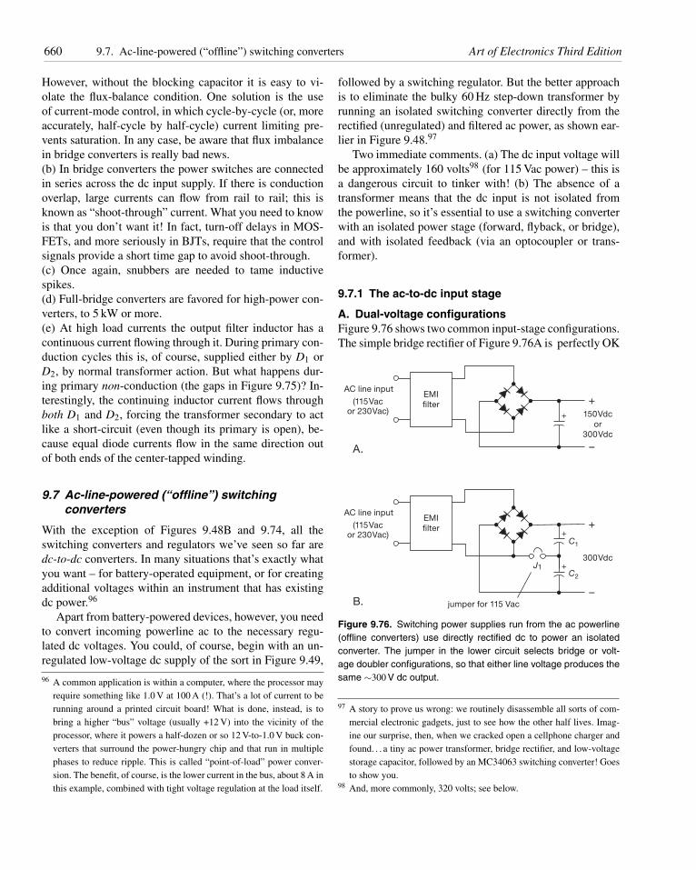
660 9.7. Ac-line-powered (“offline”) switching converters Art of Electronics Third Edition
However, without the blocking capacitor it is easy to vi-olate the flux-balance condition. One solution is the useof current-mode control, in which cycle-by-cycle (or, moreaccurately, half-cycle by half-cycle) current limiting pre-vents saturation. In any case, be aware that flux imbalancein bridge converters is really bad news.(b) In bridge converters the power switches are connectedin series across the dc input supply. If there is conductionoverlap, large currents can flow from rail to rail; this isknown as “shoot-through” current. What you need to knowis that you don’t want it! In fact, turn-off delays in MOS-FETs, and more seriously in BJTs, require that the controlsignals provide a short time gap to avoid shoot-through.(c) Once again, snubbers are needed to tame inductivespikes.(d) Full-bridge converters are favored for high-power con-verters, to 5 kW or more.(e) At high load currents the output filter inductor has acontinuous current flowing through it. During primary con-duction cycles this is, of course, supplied either by D1 orD2, by normal transformer action. But what happens dur-ing primary non-conduction (the gaps in Figure 9.75)? In-terestingly, the continuing inductor current flows throughboth D1 and D2, forcing the transformer secondary to actlike a short-circuit (even though its primary is open), be-cause equal diode currents flow in the same direction outof both ends of the center-tapped winding.
9.7 Ac-line-powered (“offline”) switchingconverters
With the exception of Figures 9.48B and 9.74, all theswitching converters and regulators we’ve seen so far aredc-to-dc converters. In many situations that’s exactly whatyou want – for battery-operated equipment, or for creatingadditional voltages within an instrument that has existingdc power.96
Apart from battery-powered devices, however, you needto convert incoming powerline ac to the necessary regu-lated dc voltages. You could, of course, begin with an un-regulated low-voltage dc supply of the sort in Figure 9.49,
96 A common application is within a computer, where the processor mayrequire something like 1.0 V at 100 A (!). That’s a lot of current to berunning around a printed circuit board! What is done, instead, is tobring a higher “bus” voltage (usually +12 V) into the vicinity of theprocessor, where it powers a half-dozen or so 12 V-to-1.0 V buck con-verters that surround the power-hungry chip and that run in multiplephases to reduce ripple. This is called “point-of-load” power conver-sion. The benefit, of course, is the lower current in the bus, about 8 A inthis example, combined with tight voltage regulation at the load itself.
followed by a switching regulator. But the better approachis to eliminate the bulky 60 Hz step-down transformer byrunning an isolated switching converter directly from therectified (unregulated) and filtered ac power, as shown ear-lier in Figure 9.48.97
Two immediate comments. (a) The dc input voltage willbe approximately 160 volts98 (for 115 Vac power) – this isa dangerous circuit to tinker with! (b) The absence of atransformer means that the dc input is not isolated fromthe powerline, so it’s essential to use a switching converterwith an isolated power stage (forward, flyback, or bridge),and with isolated feedback (via an optocoupler or trans-former).
9.7.1 The ac-to-dc input stage
A. Dual-voltage configurationsFigure 9.76 shows two common input-stage configurations.The simple bridge rectifier of Figure 9.76A is perfectly OK
(115Vacor 230Vac)
A.
+EMI
filter150Vdc
or
300Vdc
–
+
B.
+EMI
filter
300Vdc
jumper for 115 Vac
C1
C2
J1
–
+
+
AC line input
(115Vacor 230Vac)
AC line input
Figure 9.76. Switching power supplies run from the ac powerline(offline converters) use directly rectified dc to power an isolatedconverter. The jumper in the lower circuit selects bridge or volt-age doubler configurations, so that either line voltage produces thesame ∼300 V dc output.
97 A story to prove us wrong: we routinely disassemble all sorts of com-mercial electronic gadgets, just to see how the other half lives. Imag-ine our surprise, then, when we cracked open a cellphone charger andfound. . . a tiny ac power transformer, bridge rectifier, and low-voltagestorage capacitor, followed by an MC34063 switching converter! Goesto show you.
98 And, more commonly, 320 volts; see below.
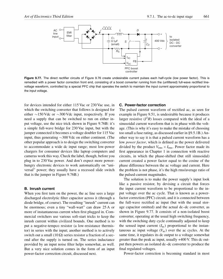
Art of Electronics Third Edition 9.7.1. The ac-to-dc input stage 661
ACline
input+
+
EMI
filter
400 Vdc
FB
PFC boostcontroller
toisolatedDC - DCconverter
C1
0.1μF(small) C2
S
RS
DL
–
IAC
VAC
Figure 9.77. The direct rectifier circuits of Figure 9.76 create undesirable current pulses each half-cycle (low power factor). This isremedied with a power factor correction front end, consisting of a boost converter running from the (unfiltered) full-wave rectified line-voltage waveform, controlled by a special PFC chip that operates the switch to maintain the input current approximately proportional tothe input voltage.
for devices intended for either 115 Vac or 230 Vac use, inwhich the switching converter that follows is designed foreither ∼150 Vdc or ∼300 Vdc input, respectively. If youneed a supply that can be switched to run on either in-put voltage, use the nice trick shown in Figure 9.76B: it’sa simple full-wave bridge for 230 Vac input, but with thejumper connected it becomes a voltage doubler for 115 Vacinput, thus generating ∼300 Vdc on either continent. (Theother popular approach is to design the switching converterto accommodate a wide dc input range; most low-powerchargers for consumer devices like laptop computers andcameras work this way. Check the label, though, before youplug in to 230 Vac power. And don’t expect more power-hungry electronic devices to work automatically on “uni-versal” power; they usually have a recessed slide switchthat is the jumper in Figure 9.76B.)
B. Inrush currentWhen you first turn on the power, the ac line sees a largedischarged electrolytic filter capacitor across it (through adiode bridge, of course). The resulting “inrush” current canbe enormous; even a tiny “wall-wart” can draw 25 A ormore of instantaneous current when first plugged in. Com-mercial switchers use various soft-start tricks to keep theinrush current within civilized bounds. One method is toput a negative-tempco resistor (a low-resistance thermis-tor) in series with the input; another method is to activelyswitch out a small (10 Ω) series resistor a fraction of a sec-ond after the supply is turned on. The series inductanceprovided by an input noise filter helps somewhat, as well.But a very nice solution comes in the form of an inputpower-factor correction circuit, discussed next.
C. Power-factor correctionThe pulsed current waveform of rectified ac, as seen forexample in Figure 9.51, is undesirable because it produceslarger resistive (I2R) losses compared with the ideal of asinusoidal current waveform that is in phase with the volt-age. (This is why it’s easy to make the mistake of choosingtoo small a fuse rating, as discussed earlier in §9.5.1B.) An-other way to say it is that a pulsed current waveform has alow power factor, which is defined as the power delivereddivided by the product Vrms × Irms. Power factor made itsfirst appearance in Chapter 1 in connection with reactivecircuits, in which the phase-shifted (but still sinusoidal)current created a power factor equal to the cosine of thephase difference between the ac voltage and current. Herethe problem is not phase, it’s the high rms/average ratio ofthe pulsed-current magnitudes.
The solution is to make the power supply’s input looklike a passive resistor, by devising a circuit that forcesthe input current waveform to be proportional to the in-put voltage over the ac cycle. That is known as a power-factor correction (PFC) circuit, and it is connected betweenthe full-wave rectified ac input (but with the usual stor-age capacitor omitted) and the actual dc–dc converter, asshown in Figure 9.77. It consists of a non-isolated boostconverter, operating at the usual high switching frequency,with the switching duty cycle continually adjusted to keepthe sensed input current (Iac) proportional to the instan-taneous ac input voltage (Vac) over the ac cycles. At thesame time, it regulates its dc output to a voltage somewhatgreater than the peak ac input, usually +400 V. This dc out-put then powers an isolated dc–dc converter to produce thefinal regulated voltages.
Power-factor correction is becoming standard in most
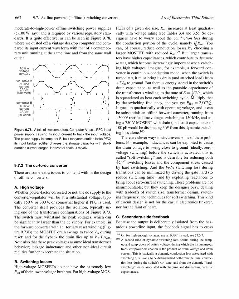
662 9.7. Ac-line-powered (“offline”) switching converters Art of Electronics Third Edition
moderate-to-high-power offline switching power supplies(>100 W, say), and is required by various regulatory stan-dards. It is quite effective, as can be seen in Figure 9.78,where we dusted off a vintage desktop computer and com-pared its input current waveform with that of a contempo-rary unit running at the same time and from the same walloutlet.
AC linevoltage
AC linecurrent
200V/div
computer A
2A/div(120 watts)
AC linecurrent
computer B
2A/div(80 watts)
Figure 9.78. A tale of two computers. Computer A has a PFC-inputpower supply, causing its input current to track the input voltage.The power supply in computer B, built ten years earlier, lacks PFC;its input bridge rectifier charges the storage capacitor with short-duration current surges. Horizontal scale: 4 ms/div.
9.7.2 The dc-to-dc converter
There are some extra issues to contend with in the designof offline converters.
A. High voltageWhether power-factor corrected or not, the dc supply to theconverter–regulator will be at a substantial voltage, typi-cally 150 V or 300 V, or somewhat higher if PFC is used.The converter itself provides the isolation, typically us-ing one of the transformer configurations of Figure 9.73.The switch must withstand the peak voltages, which canbe significantly larger than the dc supply. For example, inthe forward converter with 1:1 tertiary reset winding (Fig-ure 9.73B) the MOSFET drain swings to twice Vin duringreset; and for the flyback the drain flies up to Vin·T/toff.Note also that these peak voltages assume ideal transformerbehavior; leakage inductance and other non-ideal circuitrealities further exacerbate the situation.
B. Switching lossesHigh-voltage MOSFETs do not have the extremely lowRon of their lower-voltage brethren. For high-voltage MOS-
FETs of a given die size, Ron increases at least quadrati-cally with voltage rating (see Tables 3.4 and 3.5). So de-signers have to worry about the conduction loss duringthe conduction portion of the cycle, namely I2
DRon. Youcan, of course, reduce conduction losses by choosing alarger MOSFET, with reduced Ron.99 But larger transis-tors have higher capacitances, which contribute to dynamiclosses, which become increasingly important when switch-ing high voltages: imagine, for example, a forward con-verter in continuous-conduction mode; when the switch isturned ON, it must bring its drain (and attached load) from+2Vin to ground. But there is energy stored in the switch’sdrain capacitance, as well as the parasitic capacitance ofthe transformer’s winding, to the tune of E = 1
2CV 2, whichis squandered as heat each switching cycle. Multiply thatby the switching frequency, and you get Pdiss = 2 f CV 2
in.It goes up quadratically with operating voltage, and it canbe substantial: an offline forward converter, running from+300 V rectified line voltage, switching at 150 kHz, and us-ing a 750 V MOSFET with drain (and load) capacitance of100 pF would be dissipating 3 W from this dynamic switch-ing loss alone.100
There are clever ways to circumvent some of these prob-lems. For example, inductances can be exploited to causethe drain voltage to swing close to ground (ideally, zero-voltage switching) before the switch is activated; this iscalled “soft switching,” and is desirable for reducing both12CV 2 switching losses and the component stress causedby hard switching. And the VDID switching loss duringtransitions can be minimized by driving the gate hard (toreduce switching time), and by exploiting reactances tobring about zero-current switching. These problems are notinsurmountable; but they keep the designer busy, dealingwith tradeoffs of switch size, transformer design, switch-ing frequency, and techniques for soft switching. This kindof circuit design is not for the casual electronics tinkerer,nor for the faint of heart.
C. Secondary-side feedbackBecause the output is deliberately isolated from the haz-ardous powerline input, the feedback signal has to cross
99 Or, for high-enough voltages, use an IGBT instead; see §3.5.7.100 A second kind of dynamic switching loss occurs during the ramp-
up and ramp-down of switch voltage, during which the instantaneoustransistor power dissipation is the product of drain voltage and draincurrent. This is basically a dynamic conduction loss associated withswitching transitions, to be distinguished both from the static conduc-tion loss during the switch’s ON state, and from the dynamic “hard-switching” losses associated with charging and discharging parasiticcapacitances.
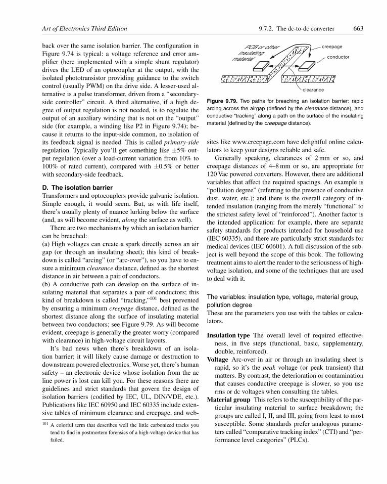
Art of Electronics Third Edition 9.7.2. The dc-to-dc converter 663
back over the same isolation barrier. The configuration inFigure 9.74 is typical: a voltage reference and error am-plifier (here implemented with a simple shunt regulator)drives the LED of an optocoupler at the output, with theisolated phototransistor providing guidance to the switchcontrol (usually PWM) on the drive side. A lesser-used al-ternative is a pulse transformer, driven from a “secondary-side controller” circuit. A third alternative, if a high de-gree of output regulation is not needed, is to regulate theoutput of an auxiliary winding that is not on the “output”side (for example, a winding like P2 in Figure 9.74); be-cause it returns to the input-side common, no isolation ofits feedback signal is needed. This is called primary-sideregulation. Typically you’ll get something like ±5% out-put regulation (over a load-current variation from 10% to100% of rated current), compared with ±0.5% or betterwith secondary-side feedback.
D. The isolation barrierTransformers and optocouplers provide galvanic isolation.Simple enough, it would seem. But, as with life itself,there’s usually plenty of nuance lurking below the surface(and, as will become evident, along the surface as well).
There are two mechanisms by which an isolation barriercan be breached:(a) High voltages can create a spark directly across an airgap (or through an insulating sheet); this kind of break-down is called “arcing” (or “arc-over”), so you have to en-sure a minimum clearance distance, defined as the shortestdistance in air between a pair of conductors.(b) A conductive path can develop on the surface of in-sulating material that separates a pair of conductors; thiskind of breakdown is called “tracking,”101 best preventedby ensuring a minimum creepage distance, defined as theshortest distance along the surface of insulating materialbetween two conductors; see Figure 9.79. As will becomeevident, creepage is generally the greater worry (comparedwith clearance) in high-voltage circuit layouts.
It’s bad news when there’s breakdown of an isola-tion barrier; it will likely cause damage or destruction todownstream powered electronics. Worse yet, there’s humansafety – an electronic device whose isolation from the acline power is lost can kill you. For these reasons there areguidelines and strict standards that govern the design ofisolation barriers (codified by IEC, UL, DIN/VDE, etc.).Publications like IEC 60950 and IEC 60335 include exten-sive tables of minimum clearance and creepage, and web-
101 A colorful term that describes well the little carbonized tracks youtend to find in postmortem forensics of a high-voltage device that hasfailed.
PCB or otherinsulating
material
creepage
clearance
conductor
Figure 9.79. Two paths for breaching an isolation barrier: rapidarcing across the airgap (defined by the clearance distance), andconductive “tracking” along a path on the surface of the insulatingmaterial (defined by the creepage distance).
sites like www.creepage.com have delightful online calcu-lators to keep your designs reliable and safe.
Generally speaking, clearances of 2 mm or so, andcreepage distances of 4–8 mm or so, are appropriate for120 Vac powered converters. However, there are additionalvariables that affect the required spacings. An example is“pollution degree” (referring to the presence of conductivedust, water, etc.); and there is the overall category of in-tended insulation (ranging from the merely “functional” tothe strictest safety level of “reinforced”). Another factor isthe intended application: for example, there are separatesafety standards for products intended for household use(IEC 60335), and there are particularly strict standards formedical devices (IEC 60601). A full discussion of the sub-ject is well beyond the scope of this book. The followingtreatment aims to alert the reader to the seriousness of high-voltage isolation, and some of the techniques that are usedto deal with it.
The variables: insulation type, voltage, material group,pollution degreeThese are the parameters you use with the tables or calcu-lators.
Insulation type The overall level of required effective-ness, in five steps (functional, basic, supplementary,double, reinforced).
Voltage Arc-over in air or through an insulating sheet israpid, so it’s the peak voltage (or peak transient) thatmatters. By contrast, the deterioration or contaminationthat causes conductive creepage is slower, so you userms or dc voltages when consulting the tables.
Material group This refers to the susceptibility of the par-ticular insulating material to surface breakdown; thegroups are called I, II, and III, going from least to mostsusceptible. Some standards prefer analogous parame-ters called “comparative tracking index” (CTI) and “per-formance level categories” (PLCs).
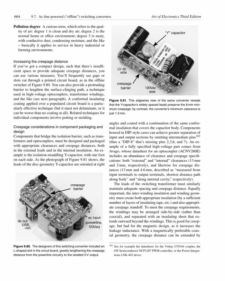
664 9.7. Ac-line-powered (“offline”) switching converters Art of Electronics Third Edition
Pollution degree A curious term, which refers to the qual-ity of air: degree 1 is clean and dry air; degree 2 is thenormal home or office environment; degree 3 is nasty,with conductive dust, condensing moisture, and the like– basically it applies to service in heavy industrial orfarming environments.
Increasing the creepage distanceIf you’ve got a compact design, such that there’s insuffi-cient space to provide adequate creepage distances, youcan use various measures. You’ll frequently see gaps orslots cut through a printed circuit board, as in the offlineswitcher of Figure 9.80. You can also provide a protrudingbarrier to lengthen the surface-clinging path, a techniqueused in high-voltage optocouplers, transformer windings,and the like (see next paragraph). A conformal insulatingcoating applied over a populated circuit board is a partic-ularly effective technique (but it must not delaminate, or itcan be worse than no coating at all). Related techniques forindividual components involve potting or molding.
Creepage considerations in component packaging anddesignComponents that bridge the isolation barrier, such as trans-formers and optocouplers, must be designed and packagedwith appropriate clearances and creepage distances, bothin the external leads and in the internal insulation. An ex-ample is the isolation-straddling Y-capacitor, with one footon each side. As the photograph of Figure 9.81 shows, theleads of the disc-geometry Y-capacitor are oriented at right
Figure 9.80. The designers of this switching converter included anL-shaped slot in the circuit board, greatly lengthening the creepagedistance from the powerline circuitry to the isolated 5 V output.
Figure 9.81. This edgewise view of the same converter revealsthat the Y-capacitor’s widely spaced leads preserve the 8 mm min-imum creepage; by contrast, the converter’s minimum clearance isjust 1.5 mm.
angles and coated with a continuation of the same confor-mal insulation that covers the capacitor body. Componentshoused in DIP-style cases can achieve greater separation ofinput and output sections by omitting intermediate pins102
(thus a “DIP-8” that’s missing pins 2,3,6, and 7). An ex-ample of a fully specified high-voltage part comes fromAvago, whose datasheet for an optocoupler (ACNV260E)includes an abundance of clearance and creepage specifi-cations: both “external” and “internal” clearances (13 mmand 2 mm, respectively), and likewise for creepage dis-tances (13 mm and 4.6 mm, described as “measured frominput terminals to output terminals, shortest distance pathalong body” and “along internal cavity,” respectively).
The leads of the switching transformer must similarlymaintain adequate spacing and creepage distance. Equallyimportant, the inter-winding insulation and winding geom-etry must create both appropriate insulation (by a sufficientnumber of layers of insulating tape, etc.) and also appropri-ate creepage standoff. To meet the creepage requirements,the windings may be arranged side-by-side (rather thancoaxial), and separated with an insulating sheet that ex-tends outward beyond the windings. This is good for creep-age, but bad for the magnetic design, as it increases theleakage inductance. With a magnetically preferable coax-ial geometry, the creepage distance can be extended by
102 See for example the datasheets for the Vishay CNY64 coupler, theON Semiconductor NCP1207 PWM controller, or the Power Integra-tions LNK-403 driver.
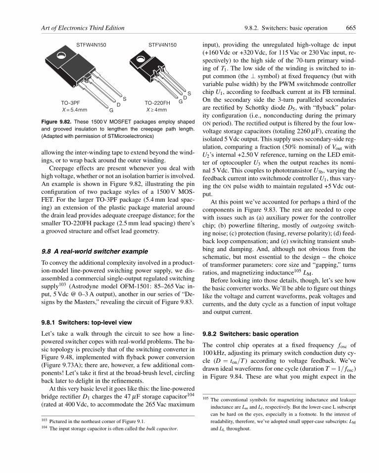
Art of Electronics Third Edition 9.8.2. Switchers: basic operation 665
TO-220FH
STFV4N150STFW4N150
GD
S GD
S
TO-3PFX = 5.4mm X ≥ 4mm
Figure 9.82. These 1500 V MOSFET packages employ shapedand grooved insulation to lengthen the creepage path length.(Adapted with permission of STMicroelectronics)
allowing the inter-winding tape to extend beyond the wind-ings, or to wrap back around the outer winding.
Creepage effects are present whenever you deal withhigh voltage, whether or not an isolation barrier is involved.An example is shown in Figure 9.82, illustrating the pinconfiguration of two package styles of a 1500 V MOS-FET. For the larger TO-3PF package (5.4 mm lead spac-ing) an extension of the plastic package material aroundthe drain lead provides adequate creepage distance; for thesmaller TO-220FH package (2.5 mm lead spacing) there’sa grooved structure and offset lead geometry.
9.8 A real-world switcher example
To convey the additional complexity involved in a product-ion-model line-powered switching power supply, we dis-assembled a commercial single-output regulated switchingsupply103 (Astrodyne model OFM-1501: 85–265 Vac in-put, 5 Vdc @ 0–3 A output), another in our series of “De-signs by the Masters,” revealing the circuit of Figure 9.83.
9.8.1 Switchers: top-level view
Let’s take a walk through the circuit to see how a line-powered switcher copes with real-world problems. The ba-sic topology is precisely that of the switching converter inFigure 9.48, implemented with flyback power conversion(Figure 9.73A); there are, however, a few additional com-ponents! Let’s take it first at the broad-brush level, circlingback later to delight in the refinements.
At this very basic level it goes like this: the line-poweredbridge rectifier D1 charges the 47 μF storage capacitor104
(rated at 400 Vdc, to accommodate the 265 Vac maximum
103 Pictured in the northeast corner of Figure 9.1.104 The input storage capacitor is often called the bulk capacitor.
input), providing the unregulated high-voltage dc input(+160 Vdc or +320 Vdc, for 115 Vac or 230 Vac input, re-spectively) to the high side of the 70-turn primary wind-ing of T1. The low side of the winding is switched to in-put common (the ⊥ symbol) at fixed frequency (but withvariable pulse width) by the PWM switchmode controllerchip U1, according to feedback current at its FB terminal.On the secondary side the 3-turn paralleled secondariesare rectified by Schottky diode D5, with “flyback” polar-ity configuration (i.e., nonconducting during the primaryON period). The rectified output is filtered by the four low-voltage storage capacitors (totaling 2260 μF), creating theisolated 5 Vdc output. This supply uses secondary-side reg-ulation, comparing a fraction (50% nominal) of Vout withU2’s internal +2.50 V reference, turning on the LED emit-ter of optocoupler U3 when the output reaches its nomi-nal 5 Vdc. This couples to phototransistor U3b, varying thefeedback current into switchmode controller U1, thus vary-ing the ON pulse width to maintain regulated +5 Vdc out-put.
At this point we’ve accounted for perhaps a third of thecomponents in Figure 9.83. The rest are needed to copewith issues such as (a) auxiliary power for the controllerchip; (b) powerline filtering, mostly of outgoing switch-ing noise; (c) protection (fusing, reverse polarity); (d) feed-back loop compensation; and (e) switching transient snub-bing and damping. And, although not obvious from theschematic, but most essential to the design – the choiceof transformer parameters: core size and “gapping,” turnsratios, and magnetizing inductance105 LM.
Before looking into those details, though, let’s see howthe basic converter works. We’ll be able to figure out thingslike the voltage and current waveforms, peak voltages andcurrents, and the duty cycle as a function of input voltageand output current.
9.8.2 Switchers: basic operation
The control chip operates at a fixed frequency fosc of100 kHz, adjusting its primary switch conduction duty cy-cle (D = ton/T ) according to voltage feedback. We’vedrawn ideal waveforms for one cycle (duration T = 1/ fosc)in Figure 9.84. These are what you might expect in the
105 The conventional symbols for magnetizing inductance and leakageinductance are Lm and Ll , respectively. But the lower-case L subscriptcan be hard on the eyes, especially in a footnote. In the interest ofreadability, therefore, we’ve adopted small upper-case subscripts: LM
and LL throughout.
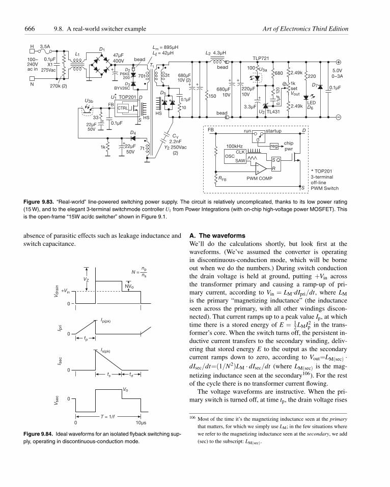
666 9.8. A real-world switcher example Art of Electronics Third Edition
H 3.5A
L1
D1
270k (2)
+
U3bFB
CTRL
HSHS
FB
RFB
run
PWM COMP
chip
pwrreg100kHz
CLK
SAWOSC
startup
+
+
+
1k
D4 CY
2.2nF
Y2 250Vac
(2)
bead
bead
TLP721
100
U2
U3a
TL431bead
150
10
70t
Lm = 895μH
Ll = 42μH L2 4.3μH
3t
7t
D3BYV26C
33
N
100–240Vac in
0.1μFX1
275Vac
47μF
400V
680μF10V (2)
680μF
10V
220μF
10V
0.1
μF
0.1μF
+
22μF50V
22μF
50V
0.1μF
DD5
T1
S
+ ++
0.1μF
3.3μF
12
0
680 2.49k220
5.0V
0–3A
1ksetVout
2.49kLEDD6
D7
–
+
D
S
S
R
Q
+
–
TOP201
3-terminal
off-line
PWM Switch
*
U1 TOP201*
P6KE200
D2
Figure 9.83. “Real-world” line-powered switching power supply. The circuit is relatively uncomplicated, thanks to its low power rating(15 W), and to the elegant 3-terminal switchmode controller U1 from Power Integrations (with on-chip high-voltage power MOSFET). Thisis the open-frame “15W ac/dc switcher” shown in Figure 9.1.
absence of parasitic effects such as leakage inductance andswitch capacitance.
+Vin
VZ
Vo
tp
ts td
NVo
Vd
rain
Vse
c
N =np
ns
0
0
0
0
0 10μs
T = 1/f
I pri
Ip(pk)
Is(pk)
I se
c
Figure 9.84. Ideal waveforms for an isolated flyback switching sup-ply, operating in discontinuous-conduction mode.
A. The waveformsWe’ll do the calculations shortly, but look first at thewaveforms. (We’ve assumed the converter is operatingin discontinuous-conduction mode, which will be borneout when we do the numbers.) During switch conductionthe drain voltage is held at ground, putting +Vin acrossthe transformer primary and causing a ramp-up of pri-mary current, according to Vin = LM·dIpri/dt, where LM
is the primary “magnetizing inductance” (the inductanceseen across the primary, with all other windings discon-nected). That current ramps up to a peak value Ip, at whichtime there is a stored energy of E = 1
2 LMI2p in the trans-
former’s core. When the switch turns off, the persistent in-ductive current transfers to the secondary winding, deliv-ering that stored energy E to the output as the secondarycurrent ramps down to zero, according to Vout=LM(sec) ·dIsec/dt=(1/N2)LM · dIsec/dt (where LM(sec) is the mag-netizing inductance seen at the secondary106). For the restof the cycle there is no transformer current flowing.
The voltage waveforms are instructive. When the pri-mary switch is turned off, at time tp, the drain voltage rises
106 Most of the time it’s the magnetizing inductance seen at the primary
that matters, for which we simply use LM; in the few situations wherewe refer to the magnetizing inductance seen at the secondary, we add(sec) to the subscript: LM(sec).
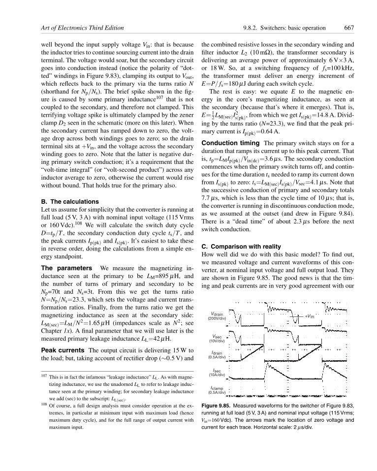
Art of Electronics Third Edition 9.8.2. Switchers: basic operation 667
well beyond the input supply voltage Vin: that is becausethe inductor tries to continue sourcing current into the drainterminal. The voltage would soar, but the secondary circuitgoes into conduction instead (notice the polarity of “dot-ted” windings in Figure 9.83), clamping its output to Vout,which reflects back to the primary via the turns ratio N(shorthand for Np/Ns). The brief spike shown in the fig-ure is caused by some primary inductance107 that is notcoupled to the secondary, and therefore not clamped. Thisterrifying voltage spike is ultimately clamped by the zenerclamp D2 seen in the schematic (more on this later). Whenthe secondary current has ramped down to zero, the volt-age drop across both windings goes to zero; so the drainterminal sits at +Vin, and the voltage across the secondarywinding goes to zero. Note that the latter is negative dur-ing primary switch conduction; it’s a requirement that the“volt-time integral” (or “volt-second product”) across anyinductor average to zero, otherwise the current would risewithout bound. That holds true for the primary also.
B. The calculationsLet us assume for simplicity that the converter is running atfull load (5 V, 3 A) with nominal input voltage (115 Vrmsor 160 Vdc).108 We will calculate the switch duty cycleD=tp/T , the secondary conduction duty cycle ts/T , andthe peak currents Ip(pk) and Is(pk). It’s easiest to take thesein reverse order, doing the calculations from a simple en-ergy standpoint.
The parameters We measure the magnetizing in-ductance seen at the primary to be LM=895 μH, andthe number of turns of primary and secondary to beNp=70t and Ns=3t. From this we get the turns ratioN=Np/Ns=23.3, which sets the voltage and current trans-formation ratios. Finally, from the turns ratio we get themagnetizing inductance as seen at the secondary side:LM(sec)=LM/N2=1.65 μH (impedances scale as N2; seeChapter 1x). A final parameter that we will use later is themeasured primary leakage inductance LL=42 μH.
Peak currents The output circuit is delivering 15 W tothe load; but, taking account of rectifier drop (∼0.5 V) and
107 This is in fact the infamous “leakage inductance” LL. As with magne-tizing inductance, we use the unadorned LL to refer to leakage induc-tance seen at the primary winding; for secondary leakage inductancewe add (sec) to the subscript: LL(sec).
108 Of course, a full design analysis must consider operation at the ex-tremes, in particular at minimum input with maximum load (hencemaximum duty cycle), and for the full range of output current withmaximum input.
the combined resistive losses in the secondary winding andfilter inductor L2 (10 mΩ), the transformer secondary isdelivering an average power of approximately 6 V×3 A,or 18 W. So, at a switching frequency of fs=100 kHz,the transformer must deliver an energy increment ofE=P/ fs=180 μJ during each switch cycle.
The rest is easy: we equate E to the magnetic en-ergy in the core’s magnetizing inductance, as seen atthe secondary (because that’s where it emerges). That is,E= 1
2 LM(sec)I2s(pk), from which we get Is(pk)=14.8 A. Divid-
ing by the turns ratio (N=23.3), we find that the peak pri-mary current is Ip(pk)=0.64 A.
Conduction timing The primary switch stays on for aduration that ramps its current up to this peak current. Thatis, tp=LMIp(pk)/Vin(dc)=3.6 μs. The secondary conductioncommences when the primary switch turns off, and contin-ues for the time duration ts needed to ramp its current downfrom Is(pk) to zero: ts=LM(sec)Is(pk)/Vsec=4.1 μs. Note thatthe successive conduction of primary and secondary totals7.7 μs, which is less than the cycle time of 10 μs; that is,the converter is running in discontinuous conduction mode,as we assumed at the outset (and drew in Figure 9.84).There is a “dead time” of about 2.3 μs before the nextswitch conduction.
C. Comparison with realityHow well did we do with this basic model? To find out,we measured voltage and current waveforms of this con-verter, at nominal input voltage and full output load. Theyare shown in Figure 9.85. The good news is that the tim-ing and peak currents are in very good agreement with our
Vdrain(200V/div)
(10V/div)
Vsec
(0.5A/div)Idrain
(10A/div)Isec
(0.5A/div)
Iclamp
+Vin
Figure 9.85. Measured waveforms for the switcher of Figure 9.83,running at full load (5 V, 3 A) and nominal input voltage (115 Vrms;Vin=160 Vdc). The arrows mark the location of zero voltage andcurrent for each trace. Horizontal scale: 2 μs/div.
668 9.8. A real-world switcher example Art of Electronics Third Edition
calculations. The bad news is that there are some real-world “features” that are absent from our basic waveformsof Figure 9.84. Most prominent are
(a) a substantial drain voltage spike at turn-off, followedby
(b) some fast ringing on both windings during secondaryconduction, and
(c) slower ringing during the dead time at the end of thecycle.
Visible also is
(d) a drain current spike at turn-on.
These are caused by non-ideal behavior of the MOSFETswitch and the transformer, as we’ll discuss soon; but, toput some names onto them, these effects are due to
(a) primary leakage inductance,(b) resonance of drain (and other) capacitances with pri-
mary leakage inductance,(c) resonance of drain (and other) capacitances with pri-
mary magnetizing inductance, and(d) “hard switching” of the voltage across the drain and
other capacitances.
9.8.3 Switchers: looking more closely
Let’s go back and fill in the missing pieces. In the realworld you cannot ignore important effects such as the volt-age and current transients that we saw in Figure 9.85, andnumerous other details that account for all the componentsyou see in the circuit diagram.
A. Input filteringBeginning at the input, we find the obligatory fuse, andthen an across-the-line “X” capacitor (§9.5.1D and follow-ing) and a series-coupled inductor pair, together forming anEMI and transient filter. It’s always a good idea, of course,to clean up the ac power entering an instrument; here, how-ever, filtering is additionally needed to keep RF hash gener-ated inside the power supply from radiating out through thepowerline.109 This is not merely an act of altruism; there
109 The important filter parameter here is not the converter’s basic switch-ing frequency, but rather the parasitic RF ringing frequency. If thelatter is 2.5 MHz, for example, a lowpass filter with 250 kHz cut-off will attenuate the RFI by approximately ( fRFI/ fLPF)2, or 100×.With the 100 nF “X1” capacitor shown, the series inductance of thecommon-mode choke (its transformer leakage inductance) need beonly L=1/(2π fLPF)2CX=4 μH. Higher frequencies will be attenuated
are regulatory standards governing permissible levels of ra-diated and conducted EMI.110 The pair of 270k resistorsdischarges the X capacitor’s residual voltage when the unitis unplugged.
B. Voltage range, inrush current, PFCNote that this low-power (15 W) supply operates directlyfrom a wide input voltage range (3:1), without a dual-voltage range switch in the manner of Figure 9.76B. Suchwide-range operation is particularly convenient in chargersand power bricks for consumer electronics. It does, how-ever, impose constraints on the design, because the con-verter must operate over a wide range of switch conductionduty cycle, and because the components must be sized forthe wider range of peak voltages and currents. Absent, also,are any circuit elements to limit the inrush current duringinitial charging of the line-side storage capacitor. That’spermissible in a small supply like this; but even with therelatively small 47 μF storage capacitor the specified typ-ical inrush current is a hefty 20 A at 100 Vac input (andtwice that for 200 Vac). Note also the absence of a PFCfrontend; it’s common practice to omit PFC in small sup-plies, but PFC is usually found in supplies of 50 W or more,at least in part from regulatory pressures. Note, by the way,that a PFC front-end reduces peak inrush current.
C. Auxiliary supplyMoving to the right, we see the interesting configurationof the “auxiliary supply,” needed to power the internalcircuits of the regulator–controller chip with low-voltage,low-power dc. An unattractive possibility would be to usea separate little linear supply, with its own line-poweredtransformer, etc. However, the temptation is overwhelm-ing to hang another small winding (with half-wave rectifierD4) on T1, thus saving a separate transformer. That’s what’sbeen done here, with the 7-turn winding, which generatesa nominal +12 V output.
Sharp-eyed readers will have noticed a flaw in thisscheme: the circuit cannot start itself, because the auxil-iary dc is present only if the supply is already running!This turns out to be an old problem,111 solved with a “kick-
more, up to the frequency at which the PCB’s wiring inductance andthe choke’s winding self-capacitance take over.
110 In the US, electronic equipment must meet FCC Class A (for indus-trial settings) and Class B (more stringent, for residential settings)limits; in Europe the analogous standards are set by VDE.
111 For example, designers of traditional CRT-based television sets facedthe same quandary, when they derived all their low-voltage dc sup-plies from auxiliary windings on the high-frequency horizontal drivetransformer, the latter itself activated by those same supplies.
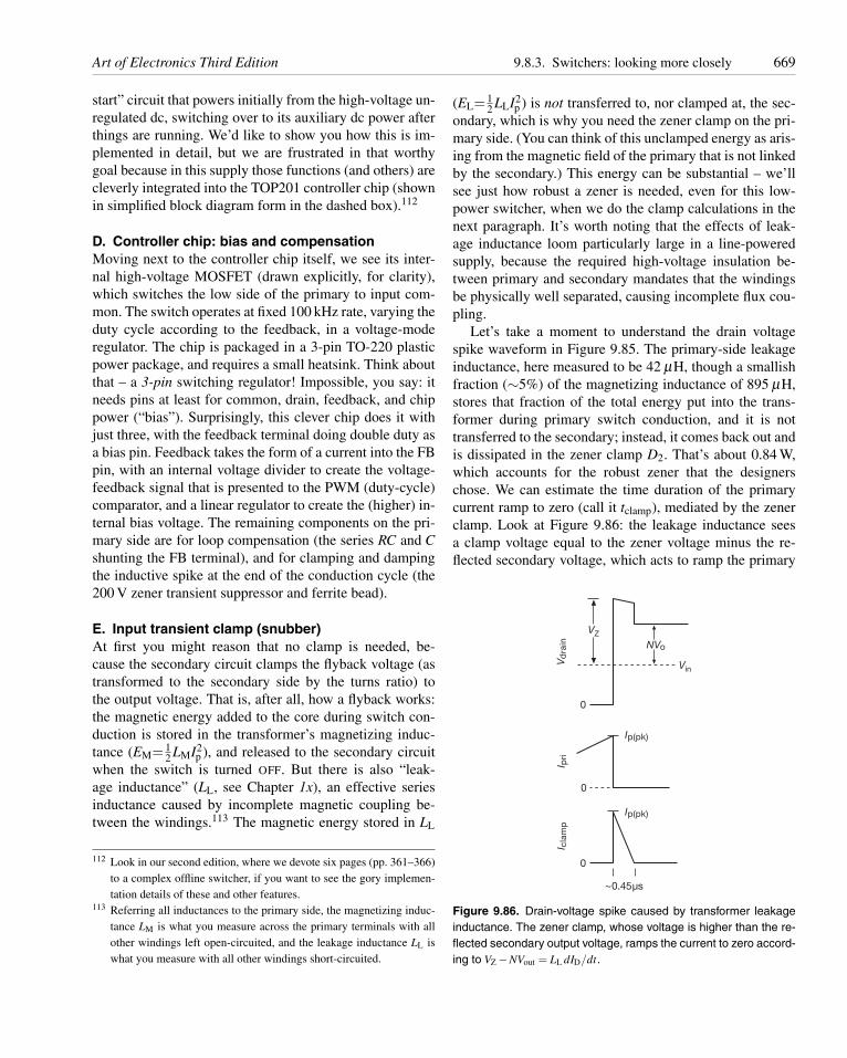
Art of Electronics Third Edition 9.8.3. Switchers: looking more closely 669
start” circuit that powers initially from the high-voltage un-regulated dc, switching over to its auxiliary dc power afterthings are running. We’d like to show you how this is im-plemented in detail, but we are frustrated in that worthygoal because in this supply those functions (and others) arecleverly integrated into the TOP201 controller chip (shownin simplified block diagram form in the dashed box).112
D. Controller chip: bias and compensationMoving next to the controller chip itself, we see its inter-nal high-voltage MOSFET (drawn explicitly, for clarity),which switches the low side of the primary to input com-mon. The switch operates at fixed 100 kHz rate, varying theduty cycle according to the feedback, in a voltage-moderegulator. The chip is packaged in a 3-pin TO-220 plasticpower package, and requires a small heatsink. Think aboutthat – a 3-pin switching regulator! Impossible, you say: itneeds pins at least for common, drain, feedback, and chippower (“bias”). Surprisingly, this clever chip does it withjust three, with the feedback terminal doing double duty asa bias pin. Feedback takes the form of a current into the FBpin, with an internal voltage divider to create the voltage-feedback signal that is presented to the PWM (duty-cycle)comparator, and a linear regulator to create the (higher) in-ternal bias voltage. The remaining components on the pri-mary side are for loop compensation (the series RC and Cshunting the FB terminal), and for clamping and dampingthe inductive spike at the end of the conduction cycle (the200 V zener transient suppressor and ferrite bead).
E. Input transient clamp (snubber)At first you might reason that no clamp is needed, be-cause the secondary circuit clamps the flyback voltage (astransformed to the secondary side by the turns ratio) tothe output voltage. That is, after all, how a flyback works:the magnetic energy added to the core during switch con-duction is stored in the transformer’s magnetizing induc-tance (EM= 1
2 LMI2p ), and released to the secondary circuit
when the switch is turned OFF. But there is also “leak-age inductance” (LL, see Chapter 1x), an effective seriesinductance caused by incomplete magnetic coupling be-tween the windings.113 The magnetic energy stored in LL
112 Look in our second edition, where we devote six pages (pp. 361–366)to a complex offline switcher, if you want to see the gory implemen-tation details of these and other features.
113 Referring all inductances to the primary side, the magnetizing induc-tance LM is what you measure across the primary terminals with allother windings left open-circuited, and the leakage inductance LL iswhat you measure with all other windings short-circuited.
(EL= 12 LLI2
p ) is not transferred to, nor clamped at, the sec-ondary, which is why you need the zener clamp on the pri-mary side. (You can think of this unclamped energy as aris-ing from the magnetic field of the primary that is not linkedby the secondary.) This energy can be substantial – we’llsee just how robust a zener is needed, even for this low-power switcher, when we do the clamp calculations in thenext paragraph. It’s worth noting that the effects of leak-age inductance loom particularly large in a line-poweredsupply, because the required high-voltage insulation be-tween primary and secondary mandates that the windingsbe physically well separated, causing incomplete flux cou-pling.
Let’s take a moment to understand the drain voltagespike waveform in Figure 9.85. The primary-side leakageinductance, here measured to be 42 μH, though a smallishfraction (∼5%) of the magnetizing inductance of 895 μH,stores that fraction of the total energy put into the trans-former during primary switch conduction, and it is nottransferred to the secondary; instead, it comes back out andis dissipated in the zener clamp D2. That’s about 0.84 W,which accounts for the robust zener that the designerschose. We can estimate the time duration of the primarycurrent ramp to zero (call it tclamp), mediated by the zenerclamp. Look at Figure 9.86: the leakage inductance seesa clamp voltage equal to the zener voltage minus the re-flected secondary voltage, which acts to ramp the primary
Vin
VZ
Vd
rain NVo
0
0
0
~0.45μs
I pri
Ip(pk)
Ip(pk)
I cla
mp
Figure 9.86. Drain-voltage spike caused by transformer leakageinductance. The zener clamp, whose voltage is higher than the re-flected secondary output voltage, ramps the current to zero accord-ing to VZ −NVout = LL dID/dt.
670 9.8. A real-world switcher example Art of Electronics Third Edition
current down to zero from its starting value of Ip(pk).So, from V=LdI/dt we get VZ−NVout=LLIp(pk)/tclamp, sotclamp=0.45 μs. This is in good agreement with the mea-sured waveforms of Figure 9.85.
A final note on the clamp network: the zener D2 is not anormal zener, but rather a “transient voltage suppressor”type (TVS; see discussion in Chapter 9x), designed andspecified to absorb large pulses of energy. The series diodeD3 is needed to prevent conduction during the switch-ON
cycle, when the zener would conduct as a normal diode.There’s an interesting problem associated with D3, namelythe fact that ordinary diodes have a “reverse recovery time”after forward conduction, which is due to charge storage ef-fects, before they become non-conducting (this is the ori-gin of the curious microsecond-scale spikes seen in a sim-ple 60 Hz unregulated power supply; see §9x.6). For thisreason D3 in this circuit is a “fast soft-recovery” rectifier:the “fast” means that it turns off quickly (<30 ns), andthe “soft” means that it does so smoothly, not abruptly.That’s useful, because an abrupt current transition to non-conduction produces large inductive spikes (V = LdI/dt).In addition, the designers added a ferrite bead to damp andsuppress such effects.
F. The transformerIn a flyback converter the primary and secondary conduc-tion cycles do not overlap (as they do in, say, a forwardconverter). So all the energy that is being moved from pri-mary to secondary must take up temporary residence in thetransformer’s core. That is, in a flyback converter the trans-former is not “just a transformer”: in addition to the usualtransformer functions (voltage and current transformationby the turns ratio, and galvanic isolation), it is also an in-ductor, storing energy from the primary cycle in its magne-tizing inductance to the tune of E= 1
2 LMIp(pk). In fact, it’sprobably more accurate to think of it as “an inductor witha secondary winding.” To enhance the energy storage func-tions, such transformers are usually designed with a delib-erate gap in the magnetic material, which has the effect ofraising the stored energy for a given applied volt-secondproduct. This particular transformer is evidently gapped,because its value of AL (the ratio of magnetizing induc-tance to turns squared) is low: AL=LM/N2
p =183 nH/t2,compared with a value of the order of 1500 for an ungappedferrite core of this size. (The nonconducting ferrite core isused to eliminate eddy current losses at the high operatingfrequency.)
As we discovered above, this converter runs in discon-tinuous conduction mode at nominal input voltage and fullload current. In fact, it stays in DCM even at minimum in-
put voltage (90 Vrms) and full load current, which is thecombination that brings it closest to CCM. With a bit moretransformer inductance it would enter CCM; presumablythe design choice was based on the desire to keep it small,and also to avoid some issues associated with CCM.114
As we hinted earlier, the transformer’s inductances areresponsible for the ringing seen in the waveforms of Fig-ure 9.85. Let’s do a simple calculation of what frequencieswe expect. During secondary conduction (immediately fol-lowing primary switch turn-off) the primary circuit lookslike a parallel LC, with leakage inductance LL in parallelwith the parasitic capacitances of the MOSFET and othercomponents (clamp diode, primary winding). A reason-able estimate for the combined capacitances is somethinglike 75 pF, due mostly to the transformer wiring and theclamp zener. So the parallel LC formed with the leakageinductance of 42 μH resonates at about 2.8 MHz, in goodagreement with the observed ringing (∼2.5 MHz). At thecompletion of secondary conduction, the primary side nolonger sees the leakage inductance (because the secondaryis no longer clamped by the load); instead it sees the mag-netizing inductance LM of 895 μH (because the secondaryis now open-circuited).115 The new calculated resonant fre-quency then drops to about 615 kHz. You can see the firsthalf-cycle of this slower resonance in the measured wave-forms, centered on the +160 V dc input voltage, and inter-rupted by the onset of the next conduction cycle. (We laterran the converter at 25% load, which allowed three cyclesof ringing at ∼600 kHz, in excellent agreement with thisestimate.)
While we’re on the subject of parasitic capacitances,this is a good time to note the ∼0.3 A current spikes atswitch turn-on. This occurs because the switch is abruptlyshorting a charged capacitor (the parallel capacitance of114 Most notably some tendency for the output voltage to overshoot when
there is an abrupt drop in load current (owing to a larger required in-ductance in a CCM design, perhaps influenced also by the nonzeromagnetic field throughout the cycle), and also a change in the feed-back loop behavior (because of the different functional dependence ofoutput voltage versus duty cycle, and, more interestingly, the fact thatin CCM the duty cycle is fixed, for a given output voltage, and is inde-pendent of load current). Given this last fact, it may seem paradoxicalthat regulation against changes in load current is even possible! Whathappens is that, once in CCM, a change in load current causes a tran-
sient change in duty cycle, such that the baseline (minimum) primarycurrent moves up or down to accommodate the changed load current;having established that new baseline current, the duty cycle then re-turns to the fixed value appropriate to the regulated output voltage.
115 Somewhat overdamped by the reflected impedance of about 5 kΩ inseries with ∼200 pF from the 10Ω+0.1 μF secondary snubber net-work.
Art of Electronics Third Edition 9.8.4. The “reference design” 671
the switch itself, plus attached components). This is called“hard switching,” and is responsible for significant powerlosses in converters running at high switching frequencies.Here, for instance, we can estimate the power dissipatedin the switch by multiplying 1
2CV 2 by the switching fre-quency, giving Pdiss ≈ 0.15 W. That’s not too serious at thismodest switching frequency of 100 kHz, being just 1% ofthe output power; but its relative contribution is greater atlow load current, and in any case it contributes to switchdissipation and stress. And it becomes increasingly impor-tant as you try to increase the switching frequency (in orderto reduce size). The solution is to strive for “soft switch-ing,” in which the voltage across the switch is brought closeto zero before switch activation (by exploiting reactive cur-rents to discharge parasitic capacitances); this goal is called“zero-voltage switching” (ZVS).
G. Secondary power trainMoving to the secondary side, the rectifier is a Schottkytype, which has both low forward voltage drop and zero re-covery time (absence of charge storage).116 Schottky rec-tifiers (also known as hot carrier rectifiers) are availableat voltages up to ∼100 V; above that you’d use a “fast-recovery” (or “fast soft-recovery,” like D3) rectifier. Powerrectifiers often come packaged as duals for applicationsthat require two; here they’ve simply connected them inparallel. Note the heatsink: 3 A of average load currentflowing through a 0.5 V (Schottky) forward drop dissipates1.5 W, enough to merit a small heatsink. The series RCprovides some damping and attenuation of switching tran-sients, as do the ferrite beads. The series inductor L2 fil-ters ripple at the switching frequency: its reactance at the100 kHz switching frequency is 2.7 Ω, compared with animpedance of ∼0.1Ω (dominated by series resistance) forthe downstream storage capacitors.
H. Secondary regulationThis power supply uses the popular TL431 “shunt regula-tor,” which includes an internal voltage reference and er-ror amplifier, and which goes into heavy conduction whenthe reference pin reaches 2.5 V above the ground pin. Thatturns on the optocoupler U3’s LED emitter, for currentsabove about 2 mA (the threshold set by the 680 Ω resis-tor). The resistive divider and trimmer allow ±0.4 V outputadjustment, and the series RC around the TL431 is a com-
116 To deal with the high 15 A peak current in D5, the designers selecteda YG802C04 Schottky rectifier with its pair of 40 V 10 A sectionsparalleled (each of which specifies a forward drop of 0.53 V at 7 A),attached to its own heatsink.
pensation network to prevent oscillation. The large shuntcapacitor limits the loop bandwidth, and also accomplishes“soft-start” at power-on: this it does by tricking the opto-emitter into thinking that the TL431 is conducting, whenin fact the LED current is coming from the ramp-up of out-put voltage. It’s easy to verify that an output ramp-up of1.5 V/ms produces a sinking current of 5 mA at the cathodeof the optocoupler LED, thus stretching the startup to about3 ms, and therefore setting the secondary current neededto charge the four output storage capacitors to ∼3.4 A,roughly equal to the supply’s maximum current rating.
I. Other design featuresThere are just a few additional goodies in this circuit. Ca-pacitor CY is used to suppress conducted EMI. Because itbridges the isolation barrier, it must have appropriate “Y-capacitor” safety ratings (see §9.5.1). Rectifier D7 protectsagainst reverse polarity, in case some misbehaving load de-cides to create mayhem. The small output capacitor ensureslow output impedance at high frequencies, where the largeelectrolytic capacitors become less effective (owing to in-ternal inductance and ESR). And, finally, the switchmodecontroller itself (U1) includes a host of nice features: in-ternal oscillator requiring no external timing components,internal cycle-by-cycle current limit, overtemperature pro-tection, automatic restart, internal regulator and dc sourceswitching, and on-chip high-voltage power MOSFET, allintegrated in an elegant 3-terminal configuration. Its highlevel of integration stole our thunder: it robbed us of theopportunity to show these important circuits explicitly!
9.8.4 The “reference design”
This is a nice power supply. We’ve bought a lot of them,and they work reliably and well. The circuit design mightseem forbiddingly complicated, certainly for those inexpe-rienced in offline switchmode supply design. In fact, werecommend strongly that the user of such supplies shouldnot try to design and build them – buy them from the expertfolks who do this for a living (see below).
But, how did those experts come up with this particu-lar design? As it turns out, the manufacturers of interestingICs have a great interest in making it painless to use theirproducts. For this noble objective they provide what areknown as reference designs, which basically consist of acomplete circuit example (usually available from them as a“development board” or “evaluation board”). For the regu-lator chip used in this particular power supply, for example,Power Integrations (the TOP201 manufacturer) providesfour example circuits, with increasing levels of regulation
672 9.8. A real-world switcher example Art of Electronics Third Edition
stability (called “minimum parts count,” “enhanced min-imum parts count,” “simple optocoupler feedback,” and“accurate optocoupler feedback”). And in a pair of “Ap-plication Notes”117 they provide a step-by-step recipe forthese designs, complete with flowcharts, formulas, andgraphs. You can hardly go wrong. The supply of Fig-ure 9.83, in fact, closely follows the “accurate optocou-pler feedback” design, differing primarily in the inclusionof soft start, ferrite beads, and reverse polarity protection.This is not to say that the design is a trivial exercise – theimplementation of the transformer, the packaging and lay-out, and the process of testing and regulatory approval areall major challenges.
9.8.5 Wrapup: general comments on line-poweredswitching power supplies
• Line-powered switchers are ubiquitous, and for good rea-sons. Their high efficiency keeps them cool, and the ab-sence of a low-frequency transformer makes them con-siderably lighter and smaller than the equivalent linearsupply. As a result, they are used almost exclusively topower industrial and consumer electronics.
• Switchers are noisy! Their outputs have tens of milli-volts of switching ripple; they put garbage onto the pow-erline; and they can even scream audibly! One cure foroutput ripple, if that’s a problem, is to add an externalhigh-current LC lowpass filter; alternatively, you can adda low-dropout linear post-regulator.118 Some commer-cial converters include this feature, as well as completeshielding and extensive input filtering.
• Switchers with multiple outputs are available and arepopular in computer systems. However, the separate out-puts are generated from additional windings on a com-mon transformer. Typically, feedback is taken from thehighest current output (usually the +3.3 V or +5V out-put), which means that the other outputs are not particu-larly well regulated. There is usually a “cross-regulation”specification, which tells, for example, how much the+12 V output, say, changes when you vary the load onthe +5 V output from 75% of full load to either 50% or100% of full load; a typical cross-regulation specificationis 5%. Some multiple-output switchers achieve excellentregulation by using linear post-regulators on the auxiliaryoutputs, but this is the exception. Check the specs!
117 AN-14: “TOPSwitch Tips, Techniques, and Troubleshooting Guide”;AN-16: “TOPSwitch Flyback Design Methodology.”
118 You can get a switcher and LDO combined as a single regulator IC, forexample in the Micrel “High Efficiency Low Dropout” (HELDO™)series.
• Line-powered switchers, like other switching converters,may have a minimum load-current requirement. If yourload current could drop below the minimum, you’ll haveto add some resistive loading; otherwise the output maysoar or oscillate.
• When working on a line-powered switcher, watch out!This is no empty warning – you can get yourself killed.Many components are at or above line potential and canbe lethal. You can’t clip the ground of your ’scope probeto the circuit without catastrophic consequences! (Use a1:1 isolation transformer at the input, if you must go pok-ing around.)
• Switchers usually include overvoltage “shutdown” cir-cuitry, analogous to our SCR crowbar circuits, in casesomething goes wrong. However, this circuit often is sim-ply a zener sensing circuit at the output that shuts off theoscillator if the dc output exceeds the trip point. Thereare imaginable failure modes in which such a “crow-bar” wouldn’t crowbar anything.119 For maximum safetyyou may want to add an autonomous outboard SCR-typecrowbar.
• Switchers used to have a bad reputation for reliability,but recent designs seem much better. However, whenthey decide to blow out, they sometimes do it with greatpanache! We had one blow its guts out in a “catastrophicdeconstruction,” spewing black crud all over its innardsand innocent electronic bystanders as well.
• Line-powered switchers are definitely complex and trickyto design reliably. Our advice is to avoid the design phaseentirely, by buying what you need! After all, why buildwhat you can buy?
• A switching supply, operating at roughly constant effi-ciency, presents a load that looks like a negative resis-tance (averaged over the ac wave) to the powerline thatdrives it. It can cause some crazy effects, including (butnot limited to) oscillations, when combined with the in-put reactance of noise filters.
9.8.6 When to use switchers
Luckily for you, we’re not bashful about giving advice!Here it is.119 A personal anecdote: we smelled smoke, and found a dead ’scope in
our lab one day. We opened it up, and found that the PFC’s outputstorage capacitor (470 μF, 450 V) had failed, exuding lots of gooeystuff. No problem, we thought, we’ll just replace it; especially sincea new supply costs $800! Power on, looks good, go to lunch. . . comeback, smoke! Turns out the PFC controller chip failed in a way thatprevented both regulation and overvoltage shutdown, so the boost cir-cuit just kept boosting, until the capacitor cried uncle.
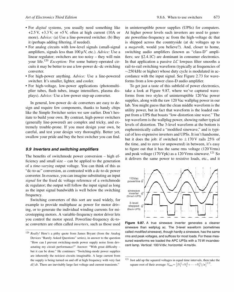
Art of Electronics Third Edition 9.8.6. When to use switchers 673
• For digital systems, you usually need something like+2.5 V, +3.3 V, or +5 V, often at high current (10A ormore). Advice: (a) Use a line-powered switcher. (b) Buyit (perhaps adding filtering, if needed).
• For analog circuits with low-level signals (small-signalamplifiers, signals less than 100 μV, etc.). Advice: Use alinear regulator; switchers are too noisy – they will ruinyour life.120 Exception: For some battery-operated cir-cuits it may be better to use a low-power dc–dc switchingconverter.
• For high-power anything. Advice: Use a line-poweredswitcher. It’s smaller, lighter, and cooler.
• For high-voltage, low-power applications (photomulti-plier tubes, flash tubes, image intensifiers, plasma dis-plays). Advice: Use a low-power step-up converter.
In general, low-power dc–dc converters are easy to de-sign and require few components, thanks to handy chipslike the Simple Switcher series we saw earlier. Don’t hes-itate to build your own. By contrast, high-power switchers(generally line-powered) are complex and tricky, and ex-tremely trouble-prone. If you must design your own, becareful, and test your design very thoroughly. Better yet,swallow your pride and buy the best switcher you can find.
9.9 Inverters and switching amplifiers
The benefits of switchmode power conversion – high ef-ficiency and small size – can be applied to the generationof a time-varying output voltage. You can think of this as“dc-to-ac” conversion, as contrasted with a dc-to-dc powerconverter. In essence, you can imagine substituting an inputsignal for the fixed dc voltage reference of a switchmodedc regulator; the output will follow the input signal as longas the input signal bandwidth is well below the switchingfrequency.
Switching converters of this sort are used widely, forexample to provide multiphase ac power for motor driv-ing, or to generate the individual winding currents for mi-crostepping motors. A variable-frequency motor driver letsyou control the motor speed. Powerline-frequency dc-to-ac converters are often called inverters, such as those used
120 Really! Here’s a pithy quote from James Bryant (from the AnalogDevices “Rarely Asked Questions” series), in answer to the question“How can I prevent switching-mode power supply noise from dev-astating my circuit performance?” Answer: “With great difficulty –but it can be done.” He continues: “Switching-mode power suppliesare inherently the noisiest circuits imaginable. A large current fromthe supply is being turned on and off at high frequency with very fastdI/dt. There are inevitably large fast voltage and current transients.”
in uninterruptible power supplies (UPSs) for computers.At higher power levels such inverters are used to gener-ate powerline-frequency ac from the high-voltage dc thatis shipped across the countryside (at dc voltages up toa megavolt, would you believe?). And, closer to home,switching audio amplifiers (known as “class-D” ampli-fiers; see §2.4.1C) are dominant in consumer electronics.In that application a passive LC lowpass filter smooths arail-to-rail switching waveform (typically at frequencies of∼250 kHz or higher) whose duty cycle is modulated in ac-cordance with the input signal. See Figure 2.73 for wave-forms from a low-power class-D audio amplifier.
To get just a taste of this subfield of power electronics,take a look at Figure 9.87, where we’ve captured wave-forms from two styles of uninterruptible 120 Vac powersupplies, along with the raw 120 Vac wallplug power in ourlab. You might guess that the clean middle waveform is theutility power, but in fact that waveform is the loaded out-put from a UPS that boasts “low-distortion sine wave.” Thetop waveform is the wallplug power, showing rather typicallevels of distortion. The 3-level waveform at the bottom iseuphemistically called a “modified sinewave,” and is typi-cal of less-expensive inverters and UPSs. It isn’t handsome,but it does the job: if switched to ±170 V rails 25% ofthe time, and to zero (or unpowered) in between, it’s easyto figure out that it has the same rms voltage (120 Vrms)and peak voltage (170 Vpk) as a 120 Vrms sinewave.121 Soit delivers the same power to resistive loads, etc., and it
115Vacpowerline
sinewaveinverter
3-levelstepped
(Smart-UPS)
(Back-UPS)
Figure 9.87. A true sinewave inverter generates a cleanersinewave than wallplug ac. The 3-level waveform (sometimescalled modified sinewave), though hardly a sinewave, has the samerms and peak voltages, and suffices for most loads. For these mea-sured waveforms we loaded the APC UPSs with a 75 W incandes-cent lamp. Vertical: 100 V/div; horizontal: 4 ms/div.
121 Just add up the squared voltages in equal time intervals, then take thesquare root of their average: Vrms=
[(V 2
1 +V 22 + · · ·+V 2
n )/n]1/2
.
674 9.10. Voltage references Art of Electronics Third Edition
charges the input side of dc power supplies or converters tothe same voltage as would the 120 Vrms utility line power.
There’s more to think about than simply having thesame rms and peak voltage, of course. There’s distortion:the 3-level waveform has no even harmonics, but it hasstrong harmonics at all odd multiples of the fundamentalfrequency (there are various multilevel schemes to addressthis problem). Then there’s the worry about systems thatexploit zero crossings of the incoming ac power for tim-ing, for which the 3-level waveform (or any stepped wave-form with an odd number of levels) would wreak havoc.122
There’s plenty more to think about, even limiting ourselvesto the subject of multilevel inverters.123
This area of power electronics is a rich subject; but,sadly, life is finite, and so (barely) is the size of this book.
9.10 Voltage references
Quite apart from their use in integrated voltage regulators,there is frequently the need for good voltage referenceswithin a circuit. For instance, you might wish to construct aprecision regulated supply with characteristics better thanthose you can obtain using the best integrated regulators.Or you might want to construct a precision constant-currentsupply. Other applications requiring precision references(but not a precision power supply) include A/D and D/Aconverters, precision waveform generators, and accuratevoltmeters, ohmmeters, or ammeters.
Integrated voltage references come in two styles: 2-terminal (or shunt), and 3-terminal (or series). Two-terminal references act like zener diodes, maintaining aconstant voltage drop when current is flowing; the externalcircuit must provide a reasonably stable operating current.Three-terminal references (Vin, Vout, GND) act like linearvoltage regulators, with internal circuitry taking care ofbiasing the internal reference (whether a zener diode, orsomething else). In Tables 9.7 and 9.8 (on pages 677 and678, respectively) we’ve listed an abundance of currentlyavailable references of both types.
There are four different technologies used in currentlyavailable voltage references, all of which exploit somephysical effect to maintain a well-defined and stable volt-
122 One solution is a 6-interval, 4-level waveform: Vpk, Vpk/2, −Vpk/2,−Vpk, spending twice as much time at Vpk/2 as at Vpk, and neverdwelling at zero. This eliminates the 3rd harmonic (as well as all theeven harmonics), and produces 120 Vrms if Vpk=170 V.
123 A nice review is found in J. Rodriguez et al., “Multilevel inverters: asurvey of topologies, controls, and applications,” IEEE Trans. Indus.Electronics., 49, 724–738 (2002), complete with 78 references.
age – zener diodes, bandgap references, JFET pinchoff ref-erences, and floating gate references. They are all availableas stand-alone (2-terminal or 3-terminal) components; theyare also commonly incorporated as an internal voltage ref-erence within a larger IC such as an A/D converter. Let’stake them in order.
9.10.1 Zener diode
The simplest form of voltage reference is the zener diode, a2-terminal device we introduced in §1.2.6A. Basically, it isa diode operated in the reverse-bias region, where currentbegins to flow at some voltage and increases dramaticallywith further increases in voltage. To use it as a reference,you simply provide a roughly constant current; this is oftendone with a resistor from a higher supply voltage, formingthe most primitive kind of regulated supply.
Zeners are available in selected voltages from 2 to200 volts (they come in the same series of values as stan-dard 5% resistors), with power ratings from a fraction of awatt to 50 watts, and tolerances of 1% to 20%. As attrac-tive as they might seem for use as general-purpose voltagereferences (being simple, inexpensive, passive 2-terminaldevices), zeners lose their luster when you look a bit moreclosely: it is necessary to stock a selection of values, thevoltage tolerance is poor except in high-priced precisionzeners, they are noisy (above 7 V), and the zener voltagedepends on current and temperature. As an example ofthe last two effects, a 27 V zener in the popular 1N5221series of 500 mW zeners has a temperature coefficient of+0.1%/◦C, and it will change voltage by 1% when its cur-rent varies from 10% to 50% of maximum.
There is an exception to this generally poor performanceof zeners. It turns out that in the neighborhood of 6 volts,zener diodes are quiet, become very stiff against changesin current, and simultaneously achieve a nearly zero tem-perature coefficient. The graphs in Figures 9.88 and 9.89illustrate the effects.124 If you need a zener for use as a sta-ble voltage reference only, and you don’t care what volt-age it is, one possibility is to use one of the compensatedzener references constructed from a 5.6 V zener (approxi-mately) in series with a forward-biased diode – if you canfind one! (Read on. . . ) The zener voltage is chosen to give apositive coefficient to cancel the diode’s temperature coef-ficient of −2.1 mV/◦C. Temperature compensation can be
124 This peculiar behavior comes about because there are two competingmechanisms going on in zener diodes: zener effect at low voltages,with negative tempco; and avalanche breakdown at high voltages, withpositive tempco.
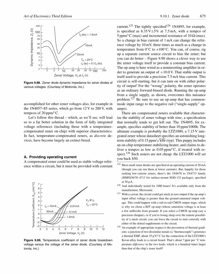
Art of Electronics Third Edition 9.10.1. Zener diode 675
200
10070
50
30
20
107
5
3
23 5 7 10 20 30 50 70 100
(dc) = 1.0mA
200
IZ
10mA
20mA
Dyn
am
ic Im
pe
dan
ce, Z
Z (Ω
)
Zener Voltage, VZ at IZ (V)
TA = 25ºC
iZ (ac) = 0.1IZ (dc)
Figure 9.88. Zener diode dynamic impedance for zener diodes ofvarious voltages. (Courtesy of Motorola, Inc.)
accomplished for other zener voltages also, for example inthe 1N4057–85 series, which go from 12 V to 200 V, withtempcos of 20 ppm/◦C.
Let’s follow this thread – which, as we’ll see, will leadus to a far better solution in the form of fully integratedvoltage references (including those with a temperature-compensated zener on-chip) with superior characteristics.In fact, temperature-compensated zeners, as discrete de-vices, have become largely an extinct breed.
A. Providing operating currentA compensated zener could be used as stable voltage refer-ence within a circuit, but it must be provided with constant
–3
–2
–1
0
1
2
3
4
5
6
7
2 3 4 5 6 7 8 9 10 11 12
IZ = 10mATA = 25ºC
30mA
0.01mA
0.1mA
1.0mA
Te
mp
era
ture
Co
effi
cie
nt,
θV
Z (m
V/º
C)
Zener Voltage, VZ (V)
VZ @ IZ
Figure 9.89. Temperature coefficient of zener diode breakdownvoltage versus the voltage of the zener diode. (Courtesy of Mo-torola, Inc.)
current.125 The tightly specified126 1N4895, for example,is specified as 6.35 V±5% at 7.5 mA, with a tempco of5 ppm/◦C (max) and incremental resistance of 10 Ω (max).So a change in bias current of 1 mA can change the refer-ence voltage by 10 mV, three times as much as a change intemperature from 0◦C to +100◦C. You can, of course, rigup a separate current source circuit to bias the zener; butyou can do better – Figure 9.90 shows a clever way to usethe zener voltage itself to provide a constant bias current.The op-amp is here wired as a noninverting amplifier in or-der to generate an output of +10.0 V. That stable output isitself used to provide a precision 7.5 mA bias current. Thiscircuit is self-starting, but it can turn on with either polar-ity of output! For the “wrong” polarity, the zener operatesas an ordinary forward-biased diode. Running the op-ampfrom a single supply, as shown, overcomes this nuisanceproblem.127 Be sure to use an op-amp that has common-mode input range to the negative rail (“single-supply” op-amps).
There are compensated zeners available that character-ize the stability of zener voltage with time, a specificationthat normally tends to get left out. The 1N4895, for ex-ample, specifies stability of better than 10 ppm/1000h. Theultimate example is probably the LTZ1000, a 7.15 V inte-grated zener whose datasheet specifies an astonishing long-term stability of 0.15 ppm/
√kHr (typ). This puppy includes
an on-chip temperature stabilizing heater, and claims to de-liver a tempco as low as 0.05 ppm/◦C, if treated with re-spect.128 Such zeners are not cheap: the LTZ1000 will setyou back $50.125 Most small zener diodes are specified at an operating current of 20 mA
(though you can run them at lower currents). But, happily for thoseseeking low-current zeners, there’s the 1N4678 to 1N4713 family(MMSZ4678–4713 for surface-mount SOD-123 package), specifiedat 50 μA.
126 And individually tested for 1000 hours! It’s available only from themanufacturer, Microsemi.
127 With a caveat: the circuit could get stuck at zero output if the op-amp’sinput offset voltage is greater than the ground-saturated output volt-age. This could happen with a rail-to-rail CMOS output stage, whichis why we chose a BJT op-amp (whose saturation voltage is at leasta few millivolts from ground). If you select a CMOS op-amp (say aprecision chopper), or if you’re losing sleep over the remote possibil-ity of a stuck circuit, you can force the circuit to start correctly witheither of the dotted supplements to the circuit.
128 An example of appropriate respect is the prevention of thermal gradi-ents: a junction of two dissimilar metals (a “thermocouple”) generatesa thermal EMF, about 35 μV/◦C for the connection of the LTZ1000’sKovar-alloy leads to a circuit board. That’s about 7 ppm per ◦C tem-perature difference in the two leads, which is a hundred times largerthan that of the chip’s zener itself!
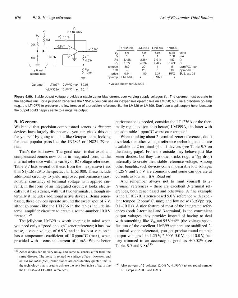
676 9.10. Voltage references Art of Electronics Third Edition
1N5232B LM329B LM399A 1N4895100k
1M
6.9V*
10k D1
R2
10.0k
V+
V+
V+
+15 to +30V
optional
startup bias
5.6
1
4.42k
7.87k
380
–
0.14
LM358A
6.9
1
3.16k
4.53k
20
20
1.80
6.95
1
3.01k
4.42k
1
8
9.37
volts
mA
Ω
Ω
ppm/ºC, max
ppm/khr
$US, qty 25
6.35
7.50
487
5.76k
5
10
RFQ
+
–R1
4.53k
*
+10.0V
LT1077
VZ
R3
R1
tempco
drift
price
op-amp
* values shown for LM329B
IZ
Op-amp: $2.082μV/°C maxLT1077
½LM358A $0.1415μV/°C max
R3 3.16k*
Figure 9.90. Stable output voltage provides a stable zener bias current over varying supply voltages V+. The op-amp must operate tothe negative rail. For a jellybean zener like the 1N5232 you can use an inexpensive op-amp like an LM358; but use a precision op-amp(e.g., the LT1077) to preserve the low tempco of a precision reference like the LM329 or LM399. Don’t use a split supply here, becausethe output could happily settle to a negative output.
B. IC zenersWe hinted that precision-compensated zeners as discretedevices have largely disappeared; you can check this outfor yourself by going to a site like Octopart.com, lookingfor once-popular parts like the 1N4895 or 1N821–29 se-ries.
That’s the bad news. The good news is that excellentcompensated zeners now come in integrated form, as theinternal reference within a variety of IC voltage references.Table 9.7 lists several of these, from the inexpensive (lessthan $1) LM329 to the spectacular LTZ1000. These includeadditional circuitry to yield improved performance (mostnotably, constancy of terminal voltage with applied cur-rent), in the form of an integrated circuit; it looks electri-cally just like a zener, with just two terminals, although in-ternally it includes additional active devices. Being zener-based, these devices operate around the sweet spot of 7 V,although some (like the LT1236 in the table) include in-ternal amplifier circuitry to create a round-number 10.0 V“zener.”129
The jellybean LM329 is worth keeping in mind whenyou need only a “good-enough” zener reference; it has lownoise, a zener voltage of 6.9 V, and in its best version ithas a temperature coefficient of 10 ppm/◦C (max), whenprovided with a constant current of 1 mA. Where better
129 Zener diodes can be very noisy, and some IC zeners suffer from thesame disease. The noise is related to surface effects, however, andburied (or subsurface) zener diodes are considerably quieter; this isthe technology that is used to achieve the very low noise of parts likethe LT1236 and LTZ1000 references.
performance is needed, consider the LT1236A or the ther-mally regulated (on-chip heater) LM399A, the latter withan admirable 1 ppm/◦C worst-case tempco!
When thinking about 2-terminal zener references, don’toverlook the other voltage reference technologies that areavailable as 2-terminal (shunt) devices (see Table 9.7 onthe facing page). From the outside they behave just likezener diodes, but they use other tricks (e.g., a VBE drop)internally to create their stable reference voltage. Amongother benefits, such devices come in desirable low voltages(1.25 V and 2.5 V are common), and some can operate atcurrents as low as 1 μA. Read on!
And remember always not to limit yourself to 2-terminal references – there are excellent 3-terminal ref-erences, both zener based and otherwise. A fine exampleis the LT1027B, a zener-based 5.0 V reference with excel-lent tempco (2 ppm/◦C, max) and low noise (3 μVpp typ,0.1–10 Hz). A nice feature of most of the integrated refer-ences (both 2-terminal and 3-terminal) is the convenientoutput voltages they provide: instead of having to dealwith something like Vout=6.95V±4% (the voltage speci-fication of the excellent LM399 temperature stabilized 2-terminal zener reference), you get precise round-numberoutput voltages like 1.25 V, 2.50 V, 5.0 V, and 10.0 V, fac-tory trimmed to an accuracy as good as ±0.02% (seeTables 9.7 and 9.8).130
130 Also powers-of-2 voltages (2.048 V, 4.096 V) to set round-numberLSB steps in ADCs and DACs.
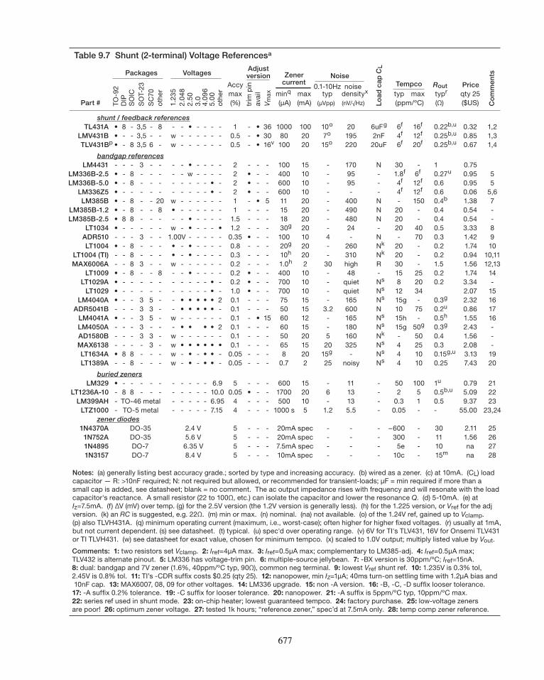
5
5
5
Table 9.7 Shunt (2-terminal) Voltage Referencesa
Co
mm
en
ts
Comments: 1: two resistors set Vclamp. 2: Iref=4μA max. 3: Iref=0.5μA max; complementary to LM385-adj. 4: Iref=0.5μA max;
TLV432 is alternate pinout. 5: LM336 has voltage-trim pin. 6: multiple-source jellybean. 7: -BX version is 30ppm/ºC; Iref=15nA.
8: dual: bandgap and 7V zener (1.6%, 40ppm/ºC typ, 90Ω), common neg terminal. 9: lowest Vref shunt ref. 10: 1.235V is 0.3% tol,
2.45V is 0.8% tol. 11: TI’s -CDR suffix costs $0.25 (qty 25). 12: nanopower, min IZ=1μA; 40ms turn-on settling time with 1.2μA bias and
10nF cap. 13: MAX6007, 08, 09 for other voltages. 14: LM336 upgrade. 15: non -A version. 16: -B, -C, -D suffix looser tolerance.
17: -A suffix 0.2% tolerance. 19: -C suffix for looser tolerance. 20: nanopower. 21: -A suffix is 5ppm/ºC typ, 10ppm/ºC max.
22: series ref used in shunt mode. 23: on-chip heater; lowest guaranteed tempco. 24: factory purchase. 25: low-voltage zeners
are poor! 26: optimum zener voltage. 27: tested 1k hours; “reference zener,” spec’d at 7.5mA only. 28: temp comp zener reference.
Packages VoltagesAdjust
Lo
ad
ca
p C
L
TO
-92
DIP
SO
IC
SO
T-2
3
SC
70
oth
er
1.2
35
2.0
48
2.5
03
.04
.09
65
.00
oth
er
trim
pin
version Zener Noise
Accy
avail
Vm
ax
current0.1-10Hz noise Tempco Rout Price
max minq max typ densityx
(ppm/ºC)
typr qty 25
Part # (%) (μA) (mA) (μVpp) (nV/√Hz)
typ max
(Ω) ($US)
shunt / feedback referencesTL431A • 8 - 3, - 8 - - • - - - - 1 - • 36 1000 100 10o 20 6uFg 6f 16f 0.22b,u 0.32 1,2
LMV431B • - - 3, - - w - - - - - - 0.5 - • 30 80 20 7o 195 2nF 4f 12f 0.25b,u 0.85 1,3
TLV431Bp • - 8 3, 6 - w - - - - - - 0.5 - • 16v 100 20 15o 220 20uF 6f 20f 0.25b,u 0.67 1,4
bandgap referencesLM4431 - - - 3 - - - - • - - - - 2 - - - 100 15 - 170 N 30 - 1 0.75
LM336B-2.5 • - 8 - - - - - w - - - - 2 • - - 400 10 - 95 - 1.8f 6f 0.27u 0.95 5
LM336B-5.0 • - 8 - - - - - - - - • - 2 • - - 600 10 - 95 - 4f 12f 0.6 0.95 5
LM336Z5 • - - - - - - - - - - • - 2 • - - 600 10 - - - 4f 12f 0.6 0.06 5,6
LM385B • - 8 - - 20 w - - - - - - 1 - • 5 11 20 - 400 N - 150 0.4b 1.38 7
LM385B-1.2 • - 8 - - 8 • - -
-
- - - - 1 - - - 15 20 - 490 N 20 - 0.4 0.54 -
LM385B-2.5 • 8 8 - - - - - • - - - - 1.5 - - - 18 20 - 480 N 20 - 0.4 0.54 -
LT1034 • - - - - - w - • - - - • 1.2 - - - 30g 20 - 24 - 20 40 0.5 3.33 8
ADR510 - - - 3 - - 1.00V - - - - 0.35 • - - 100 10 4 - N - 70 0.3 1.42 9
LT1004 • - 8 - - - • - • - - - - 0.8 - - - 20g 20 - 260 Nk 20 - 0.2 1.74 10
LT1004 (TI) - - 8 - - - • - • - - - - 0.3 - - - 10h 20 - 310 Nk 20 -
-
-
0.2 0.94 10,11
MAX6006A - - 8 3 - - w - - - - - - 0.2 - - - 1.0h 2 30 high R 30 - 1.5 1.56 12,13
LT1009 • - 8 - - 8 - - • - - - - 0.2 • - - 400 10 - 48 - 15 25 0.2 1.74 14
LT1029A • - - - - - - - - - - • - 0.2 • - - 700 10 - quiet Ns 8 20 0.2 3.34 -
LT1029 • - - - - - - - - - - • - 1.0 • - - 700 10 - quiet Ns 12 34 2.07 15
LM4040A • - - 3 5 - - • • • • • 2 0.1 - - - 75 15 - 165 Ns 15g 0.3g 2.32 16
ADR5041B - - - 3 3 - - • • • • • - 0.1 - - - 50 15 3.2 600 N 10 75 0.2u 0.86 17
LM4041A • - - 3 5 - w - - - - - - 0.1 - • 15 60 12 - 165 Ns 15h 0.5h 1.55 16
LM4050A - - - 3 -- - • • • • 2 0.1 - - - 60 15 - 180 Ns 15g 50g 0.3g 2.43 -
AD1580B - - - 3 3 - w - - - - - - 0.1 - - - 50 20 5 160 Nk - 50 0.4 1.56 -
MAX6138 - - - - 3 - w • • • • • • 0.1 - - - 65 15 20 325 Ns 4 25 0.3 2.08 -
LT1634A • 8 8 - - - w - • - • • - 0.05 - - - 8 20 15g - Ns 4 10 0.15g,u 3.13 19
LT1389A - - 8 - - - w - • - • • - 0.05 - - - 0.7 2 25 noisy Ns 4 10 0.25 7.43 20
buried zenersLM329 • - - - - - - - - - 6.9 5 - - - 600 15 - 11 - 50 100 1u 0.79 21
LT1236A-10 8 8 - - - - - - - 10.0 0.05 • - - 1700 20 6 13 - 2 5 0.5b,u 5.09 22
LM399AH TO-46 metal - - - - 6.95 4 - - - 500 10 - 13 - 0.3 1 0.5 9.37 23
LTZ1000 TO-5 metal -
-
-
- - - -
-
-
-
- 7.15 4 - - - 1000 s 5 1.2 5.5 - 0.05 - - 55.00 23,24
zener diodes1N4370A DO-35 2.4 V 5 - - - 20mA spec - - - –600 - 30 2.11 25
1N752A DO-35 5.6 V 5 - - - 20mA spec - - - 300 - 11 1.56 26
1N4895 DO-7 6.35 V 5 - - - 7.5mA spec - - - 5e - 10 na 27
1N3157 DO-7 8.4 V 5 - - - 10mA spec - - - 10c - 15m na 28
Notes: (a) generally listing best accuracy grade.; sorted by type and increasing accuracy. (b) wired as a zener. (c) at 10mA. (CL) load
capacitor — R: >10nF required; N: not required but allowed, or recommended for transient-loads; μF = min required if more than a
small cap is added, see datasheet; blank = no comment. The ac output impedance rises with frequency and will resonate with the load
capacitor's reactance. A small resistor (22 to 100Ω, etc.) can isolate the capacitor and lower the resonance Q. (d) 5-10mA. (e) at
Iz=7.5mA. (f) ΔV (mV) over temp. (g) for the 2.5V version (the 1.2V version is generally less). (h) for the 1.225 version, or Vref for the adj
version. (k) an RC is suggested, e.g. 22Ω. (m) min or max. (n) nominal. (na) not available. (o) of the 1.24V ref, gained up to Vclamp.
(p) also TLVH431A. (q) minimum operating current (maximum, i.e., worst-case); often higher for higher fixed voltages. (r) usually at 1mA,
but not current dependent. (s) see datasheet. (t) typical. (u) spec'd over operating range. (v) 6V for TI's TLV431, 16V for Onsemi TLV431
or TI TLVH431. (w) see datasheet for exact value, chosen for minimum tempco. (x) scaled to 1.0V output; multiply listed value by Vout.
677
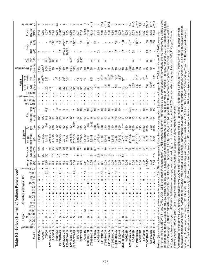
Ta
ble
9.8
S
eri
es (
3-t
erm
ina
l) V
olt
ag
e R
efe
ren
ce
sa
Filter pin
Trim pin
Shutdown pin
sense +
Pkg
sb
Referencec
Ava
ila
ble
Vo
lta
ge
sd (
V)
Comments
DIP
SOIC
SOT-23
TO-92
other
1.024
1.25
1.8
2.048
2.5
3.0
3.3
4.096
5.0
10.0
other
ADJ version
Su
pp
lyN
ois
e
Regulation
Ac
cy
Te
mp
co
ran
ge
I QI o
ut
0.1
Hz-
10
Hz
10
Hz-
10
kH
zP
ric
e
ma
xty
pm
ax
min
-ma
xty
pso
urc
esin
kty
pty
pm
ax
min
min
ma
xq
ty 2
5
Pa
rt #
(%)
(pp
m/º
C)
(V)
(μA
)(m
A)
(mA
)(μ
Vp
p)
(μV
rms)
(pp
m/V
)(μ
F)
(μF
)(μ
F)
($U
S)
LP
29
50
A-
--
•P
B-
--
--
••
-•
--
-0
.52
010
05
.4-3
010
010
0-
--
--
-4
30
r0
.1%
q1
1-
0.6
61
LP
29
51
88
-•
SB
--
--
-•
•-
•-
-•
0.5
20
12
03
.35
-30
10
010
0-
••
••
-4
30
r,s
0.1
%q
11
-0
.56
2
LT
66
50
--
5-
-B
--
--
--
--
--
0.4
j0
.75
30
-1.4
-18
5.6
0.2
0.2
--
-•
20
23
e9
00
0.1
1-
1.5
3k
3
LM
412
8A
-2.5
--
5-
-B
--
••
••
••
--
--
0.1
-75
2.9
-5.5
60
20
--
--
-275
-5
0 t
0.1
w-
10
1.8
04
AD
68
0J
88
-•
-B
--
--
•-
--
--
--
0.4
10
25
4.5
-36
20
010
--
--
-8
-16
0.1
-0
.05
3.2
05
RE
F4
3G
88
--
-B
--
--
•-
--
--
--
0.2
10
25
4.5
-40
34
02
01.2
•-
--
-7
e2
0.1
-10
6.6
66
,7
ISL
210
10
-25
--
3-
B•
•-
••
••
•-
-1.5
-0
.215
50
2.6
-5.5
46
25
1-
--
-67
37
e10
0-
0.1
10
0.7
0k
-
LM
412
0A
-2.5
--
5-
B-
-•
••
••
••
--
-0
.214
50
2.7
-12
16
05
5-
-•
-2
03
6p
80
-0
.02
20
.047
2.3
78
LM
412
5A
-2.5
--
5-
B-
--
••
--
•-
--
-0
.214
50
2.7
-616
05
5-
--
-2
03
6p
80
-0
.02
20
.11.7
58
LM
413
2A
-2.5
--
5-
B-
-•
••
••
•-
--
-0
.05
-10
2.9
-5.5
60
20
--
-•
-24
0-
50
t0
.1w
-10
2.6
04
ISL
60
00
2B
-25
--
3-
F•
••
••
••
--
-1.2
-0
.04
-2
02.7
-5.5
0.3
57
7-
--
-3
0-
10
0-
-0
.001
v5
.86
4
RE
F312
5-
-3
-B
-•
-•
••
••
--
--
0.2
515
2.5
5-6
10
010
10
--
--
33
48
25
0.4
7-
-2.0
77
RE
F3
22
5-
-6
-B
-•
-•
••
••
--
--
0.2
47
2.5
5-6
10
010
10
--
••
33
48
65
0.4
71
10
3.6
07
AD
58
4K
8-
--
- - - - - - - MB
--
--
•-
--
••
7.5
-0
.14
-15
4.5
-30
75
010
5•
••
•5
04
05
0-
--
10
.61
11
X6
00
03
B-5
0-
-3
--
F-
--
--
--
••
--
-0
.02
-10
5.1
-90
.510
10
--
--
30
-6
0-
-0
.001
v2.6
8h
7
LT
66
56
A-2
.5-
-6
-T
B-
•-
••
••
••
--
-0
.05
510
2.9
-18
0.8
55
0.1
--
--
30
80
e25
0.1
1-
6.4
24
,13
RE
F5
02
5-
8-
-S
B-
--
••
--
••
--
-0
.05
46
.55
.2-1
88
00
10
10
••
--
7.5
-1
11
50
2.9
76
AD
R3
42
5-
-6
--
B-
--
-•
•-
••
--
-0
.12.5
82.7
-5.5
85
m10
3-
-•
•18
42
50
0.1
0.1
-2.3
4-
LT
10
21B
-58
8-
--
Z-
--
--
--
-•
•7.
0-
0.1
25
7.2-3
68
00
10
10
•-
--
32.2
e12
--
-7.
00
7,14
LT
66
54
A-2
.5-
-6
-T
B-
•-
••
••
••
--
-0
.05
310
2.7
-36
35
010
10
--
--
1.5
2e
50
.11
-5
.66
4,7
,15
LT
10
19A
-2.5
88
--
-B
--
--
•-
--
••
4.5
-0
.05
35
4-3
66
50
10
10
•-
--
6.3
6.3
e3
-y
y7.
50
6,1
4
LT
C6
65
2A
-2.5
--
--
SB
-•
-•
••
••
•-
--
0.0
52
52.8
-12
35
05
5-
-•
-5
7.5
e5
0-
--
4.8
04
ISL
210
90
B-2
5-
8-
-S
B-
•-
-•
--
-•
•7.
0-
0.0
2-
73
.7-3
69
30
20
10
•-
--
1.9
1.6
e18
-0
.110
7.5
67
LT
12
36
A-5
88
--
-Z
--
--
--
--
•• •
--
0.0
52
57.
2-3
68
00
10
10
•-
--
32.2
e12
--
-5
.09
7
MA
X6
03
3A
-25
--
6-
-B
--
--
•-
•- -
--
--
0.0
41.5
72.7
-12.6
75
m15
--
-- -
•16
12
e10
-0
.110
06
.32
7
AD
R0
2B
-8
5-
-B
--
--
•-
•-
-0
.06
13
7-3
66
50
10
--
•-
10
-3
0-
--
5.0
04
Cinz
Co
ut
z
-
-
LM
414
0A
-2.5
-8
--
-B
••
-•
•-
-•
--
--
0.1
-3
2.7
-5.5
23
08
0.0
1-
-•
-2.2
-2
00
-1
x4
.7x
2.8
74
,7
AD
R4
41B
-8
--
SJ
-- -
-•
••
-•
•-
--
0.0
41
33
-18
30
00
10
5•
--
-1.2
g-
20
0.1
0.1
-6
.53
9,1
0
ISL
210
09
B2
5-
8-
-S
F-
•-
••
•-
--
--
-0
.02
-3
3.5
-16
.59
57
7•
--
-4
.52.2
e6
0-
-0
.001
v6
.11
4,7
,12
LT
C6
65
5B
-2.5
--
--
SB
-•
-•
••
••
•-
-j
0.0
25
12
3-1
35
00
05
5-
--
•0
.61.7
e25
0.1
2.7
10
08
.16
7,9,1
6
AD
R4
52
5B
-8
--
-B
--
-•
••
••
•-
--
0.0
2-
23
-15
70
010
10
--
--
1.2
5g
-10
0.1
1u
10
05
.85
9,1
7
MA
X6
32
5C
88
--
-Z
--
--
•-
-•
•-
--
0.0
40
.51
8-3
618
00
15
15
••
--
1.5
1.3
e5
--
10
013
.40
4,7
,18
No
tes: (a) so
rte
d a
pp
roxim
ate
ly b
y t
ole
ran
ce,
tem
pco
an
d 0
.1-1
0H
z n
ois
e;
gen
era
lly lis
tin
g b
est
accu
racy g
rad
e.
(b
) o
the
r p
ackag
es: M
- T
O-9
9 m
eta
l can;
P -
DP
AK
po
we
r p
kg
;
S -
sm
all
(mic
ro8
, M
SO
P); T
- t
iny (D
FN
, LC
C).
(c) B
: b
an
dg
ap
; F:
flo
atin
g g
ate
; J: JF
ET
pin
ch
off
; Z
: zen
er.
(d
) ta
bu
late
d d
ata
co
rre
sp
on
ds t
o t
he v
olt
ag
e c
ho
ice in
dic
ate
d b
y a
larg
e b
ulle
t.
(e) 10
Hz-
1kH
z.
(f)
in L
CC
pkg
. (g
) fo
r 2.5
V v
ers
ion
. (
h) q
ty 3
k.
(j) a
dju
sta
ble
via
exte
rnal re
sis
tors
. (k) q
ty 1
k.
(m
) m
in o
r m
ax.
(n) n
om
inal.
(o) 15
nV
/√H
z w
ith
CN
R=1u
F. (
p) p
eak-t
o-p
eak.
(q) o
ve
r V
in r
an
ge.
(r)
10
Hz t
o 1
00
kH
z.
(s) 10
0μV
wit
h 1
0n
F fi
lte
r cap
.
(t)
typ
ical.
(u) 0
.1μ
F f
or
V ou
t≥3V.
(v) u
p t
o 1
0u
F w
ith
re
co
mm
en
de
d p
ole
-ze
ro n
etw
ork
. (w
) a m
inim
um
of
0.1
uF
or
Co
ut,
wh
ich
eve
r is
larg
er.
(x
) E
SR
mu
st
fall
in m
in-m
ax r
an
ge, se
e d
ata
sh
eet.
(y
) n
o m
in o
r m
ax f
or
all
excep
t th
e 2
.5V
ve
rsio
n,
wh
ich
may o
scill
ate
wit
h 4
00
pF
<C
ou
t<2
μF
wh
en
sin
kin
g b
etw
een
1m
A a
nd
6m
A.
(z) a "
-" m
ean
s n
o m
inim
um
or
ma
xim
um
; in
all
case
s c
on
su
lt d
ata
sh
eet
for
deta
ils.
Co
mm
en
ts: 1
: in
exp
en
siv
e L
DO
re
g/r
ef.
2:
in
exp
en
siv
e L
DO
re
g/r
ef
wit
h d
rop
ou
t flag
; can
ad
d e
xt
BJT.
3: l
ow
est
Vre
f; o
p-a
mp
FB
in
pu
t fo
r V o
ut fr
om
0.4
V t
o r
ail.
4:
oth
er
su
ffixe
s
for
rela
xe
d t
em
pco
an
d a
ccy.
5:
-A
gra
de f
or
0.2
% a
ccy;
tem
p o
utp
ut
(in
8-p
in p
kg
s).
6: t
em
pe
ratu
re o
utp
ut.
7:
lo
ad
re
gu
latio
n 2
0p
pm
/mA
or
bett
er.
8:
no
su
ffix f
or
rela
xe
d t
em
pco
an
d a
ccy.
9:
lo
w n
ois
e,
low
tem
pco
. 1
0: a
favo
rite
. 1
1: p
in s
ele
cta
ble
Vo
ut; e
xt
resis
tors
fo
r vari
ab
le V
ou
t.
12: I
SL
210
07
fo
r V
in=
2.7
-5.5
V a
nd
I Q=
75
μA
. 1
3: 1
0m
V n
o-l
oad
dro
po
ut.
14: c
an
use in
sh
un
t m
od
e.
15:
lo
w n
ois
e,
wid
e s
up
ply
. 1
6: v
ery
lo
w n
ois
e,
low
tem
pco
. 1
7: lo
w n
ois
e,
low
tem
pco
. 1
8: lo
we
st
no
ise a
nd
tem
pco
.
AD
R42
1B
-8
--
-J
--
••
--
•-
--
0.0
41
35
-15
39
010
-•
--
-1.8
-3
5-
--
7.76
4,9
LT
10
27B
88
--
-Z
--
--
--
-•
--
-0
.02
12
8-4
02
20
015
10
••
--
32
e6
--
-6
.17
4,7
•
•
678
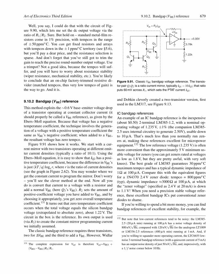
Art of Electronics Third Edition 9.10.2. Bandgap (VBE) reference 679
Well, you say, I could do that with the circuit of Fig-ure 9.90, which lets me set the dc output voltage via theratio of R1/R2. Sure. But hold on – standard metal-film re-sistors come in 1% precision, with tempcos in the rangeof ±50 ppm/◦C. You can get fixed resistors and arrayswith tempcos down in the ±1 ppm/◦C territory (see §5.6),but you’ll pay a dear price, and the resistance selection issparse. And don’t forget that you’ve still got to trim thegain to reach the precise round-number output voltage. Usea trimpot? Not a good idea, because the tempco will suf-fer, and you will have to worry about resistance stability(wiper resistance, mechanical stability, etc.). You’re likelyto conclude that an on-chip factory-trimmed resistive di-vider (matched tempcos, thus very low tempco of gain) isthe way to go. And it is.
9.10.2 Bandgap (V BE) reference
This method exploits the ∼0.6 V base–emitter voltage dropof a transistor operating at constant collector current (itshould properly be called a VBE reference), as given by theEbers–Moll equation. Because that voltage has a negativetemperature coefficient, the technique involves the genera-tion of a voltage with a positive temperature coefficient thesame as VBE’s negative coefficient; when added to a VBE,the resultant voltage has zero tempco.
Figure 9.91 shows how it works. We start with a cur-rent mirror with two transistors operating at different emit-ter current densities (typically a ratio of 10:1). Using theEbers–Moll equation, it is easy to show that IQ2 has a posi-tive temperature coefficient, because the difference in VBE’sis just (kT/q) loge r, where r is the ratio of current densities(see the graph in Figure 2.62). You may wonder where weget the constant current to program the mirror. Don’t worry– you’ll see the clever method at the end. Now all youdo is convert that current to a voltage with a resistor andadd a normal VBE (here Q3’s VBE). R2 sets the amount ofpositive-coefficient voltage you have added to VBE, and bychoosing it appropriately, you get zero overall temperaturecoefficient.131 It turns out that zero temperature coefficientoccurs when the total voltage equals the silicon bandgapvoltage (extrapolated to absolute zero), about 1.22 V. Thecircuit in the box is the reference. Its own output is used(via R3) to create the constant mirror programming currentwe initially assumed.
The classic bandgap reference requires three transistors,two for ΔVBE and the third to add a VBE. However, Widlar
131 The complete expression for Vref is therefore Vref=VBE3 +(VBE1−VBE2)R2/R1.
+5.00V
3.78k
1.22k
+VIN
VBE
+ R2IQ2
+
–Q3
Q2Q1
R2R3
R1
VBE
Figure 9.91. Classic VBE bandgap voltage reference. The transis-tor pair Q1Q2 is a ratio current mirror, typically IQ1 = 10 IQ2; that ratioputs 60 mV across R1, which sets the PTAT current IQ2.
and Dobkin cleverly created a two-transistor version, firstused in the LM317, see Figure 9.13.
IC bandgap referencesAn example of an IC bandgap reference is the inexpensive(about $0.50) 2-terminal LM385-1.2, with a nominal op-erating voltage of 1.235 V, ±1% (the companion LM385-2.5 uses internal circuitry to generate 2.50V), usable downto 10 μA. That’s much less than you normally run zen-ers at, making these references excellent for micropowerequipment.132 The low reference voltage (1.235 V) is oftenmore convenient than the approximately 5 V minimum us-able voltage for zeners (you can get zeners rated at voltagesas low as 1.8 V, but they are pretty awful, with very softknees). The best grade of LM385 guarantees 30 ppm/◦Cmaximum tempco and has a typical dynamic impedance of1Ω at 100 μA. Compare this with the equivalent figuresfor a 1N4370 2.4 V zener diode: tempco = 800 ppm/◦C(typ), dynamic impedance ≈3000Ω at 100 μA, at whichthe “zener voltage” (specified as 2.4 V at 20 mA) is downto 1.1 V! When you need a precision stable voltage refer-ence, these excellent bandgap ICs put conventional zenerdiodes to shame.
If you’re willing to spend a bit more money, you can findbandgap references of excellent stability, for example, the
132 But note that low-current references tend to be noisy: the LM385-2.5 (20 μA min) running at 100 μA has a noise voltage density of800 nV/
√Hz, compared with 120 nV/
√Hz for the analogous LT1009
or LM336-2.5 references (400 μA min) running at 1 mA. And, ifyou’re willing to squander more operating current, the LTC6655 low-noise 3-terminal bandgap reference (with a quiescent current of 5 mA)has an output noise density of just 50 nV/
√Hz, and, impressively, with
a 1/ f noise corner below 10 Hz.
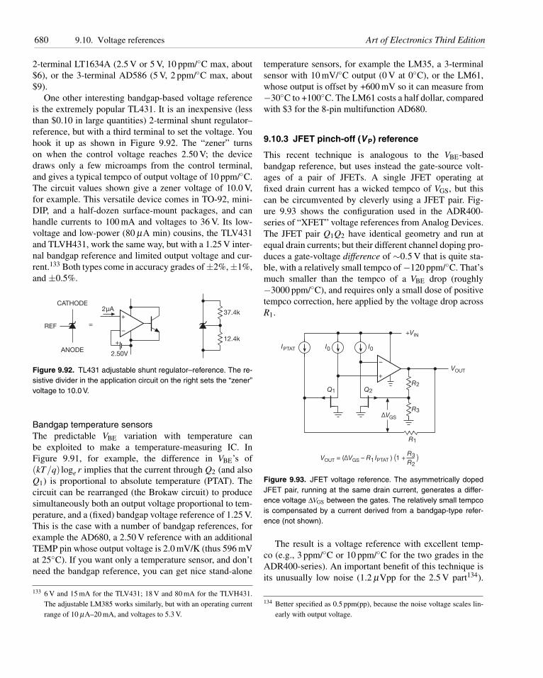
680 9.10. Voltage references Art of Electronics Third Edition
2-terminal LT1634A (2.5 V or 5 V, 10 ppm/◦C max, about$6), or the 3-terminal AD586 (5 V, 2 ppm/◦C max, about$9).
One other interesting bandgap-based voltage referenceis the extremely popular TL431. It is an inexpensive (lessthan $0.10 in large quantities) 2-terminal shunt regulator–reference, but with a third terminal to set the voltage. Youhook it up as shown in Figure 9.92. The “zener” turnson when the control voltage reaches 2.50 V; the devicedraws only a few microamps from the control terminal,and gives a typical tempco of output voltage of 10 ppm/◦C.The circuit values shown give a zener voltage of 10.0 V,for example. This versatile device comes in TO-92, mini-DIP, and a half-dozen surface-mount packages, and canhandle currents to 100 mA and voltages to 36 V. Its low-voltage and low-power (80 μA min) cousins, the TLV431and TLVH431, work the same way, but with a 1.25 V inter-nal bandgap reference and limited output voltage and cur-rent.133 Both types come in accuracy grades of ±2%, ±1%,and ±0.5%.
REF
CATHODE
ANODE
=
2.50V
2μA37.4k
12.4k
+
+
–
Figure 9.92. TL431 adjustable shunt regulator–reference. The re-sistive divider in the application circuit on the right sets the “zener”voltage to 10.0 V.
Bandgap temperature sensorsThe predictable VBE variation with temperature canbe exploited to make a temperature-measuring IC. InFigure 9.91, for example, the difference in VBE’s of(kT/q) loge r implies that the current through Q2 (and alsoQ1) is proportional to absolute temperature (PTAT). Thecircuit can be rearranged (the Brokaw circuit) to producesimultaneously both an output voltage proportional to tem-perature, and a (fixed) bandgap voltage reference of 1.25 V.This is the case with a number of bandgap references, forexample the AD680, a 2.50 V reference with an additionalTEMP pin whose output voltage is 2.0 mV/K (thus 596 mVat 25◦C). If you want only a temperature sensor, and don’tneed the bandgap reference, you can get nice stand-alone
133 6 V and 15 mA for the TLV431; 18 V and 80 mA for the TLVH431.The adjustable LM385 works similarly, but with an operating currentrange of 10 μA–20 mA, and voltages to 5.3 V.
temperature sensors, for example the LM35, a 3-terminalsensor with 10 mV/◦C output (0 V at 0◦C), or the LM61,whose output is offset by +600 mV so it can measure from−30◦C to +100◦C. The LM61 costs a half dollar, comparedwith $3 for the 8-pin multifunction AD680.
9.10.3 JFET pinch-off (V P) reference
This recent technique is analogous to the VBE-basedbandgap reference, but uses instead the gate-source volt-ages of a pair of JFETs. A single JFET operating atfixed drain current has a wicked tempco of VGS, but thiscan be circumvented by cleverly using a JFET pair. Fig-ure 9.93 shows the configuration used in the ADR400-series of “XFET” voltage references from Analog Devices.The JFET pair Q1Q2 have identical geometry and run atequal drain currents; but their different channel doping pro-duces a gate-voltage difference of ∼0.5 V that is quite sta-ble, with a relatively small tempco of −120 ppm/◦C. That’smuch smaller than the tempco of a VBE drop (roughly−3000 ppm/◦C), and requires only a small dose of positivetempco correction, here applied by the voltage drop acrossR1.
+
–
Q1 Q2
ΔVGS
R3
R2
R1
VOUT
+VIN
IPTAT I0 I0
R2
R3VOUT = (ΔVGS – R1 ) (1 + )IPTAT
Figure 9.93. JFET voltage reference. The asymmetrically dopedJFET pair, running at the same drain current, generates a differ-ence voltage ΔVGS between the gates. The relatively small tempcois compensated by a current derived from a bandgap-type refer-ence (not shown).
The result is a voltage reference with excellent temp-co (e.g., 3 ppm/◦C or 10 ppm/◦C for the two grades in theADR400-series). An important benefit of this technique isits unusually low noise (1.2 μVpp for the 2.5 V part134).
134 Better specified as 0.5 ppm(pp), because the noise voltage scales lin-early with output voltage.
Art of Electronics Third Edition 9.10.5. Three-terminal precision references 681
Bandgap references cannot match this sort of noise perfor-mance, because the process of compensating for their largeintrinsic temperature coefficient introduces the lion’s shareof their output noise.
9.10.4 Floating-gate reference
This most recent entry into the voltage reference sweep-stakes is, well, bizarre. If you were challenged to come upwith an idea that would most likely fail, you might inventthe “floating-gate array” (FGA) reference. Intersil did that,but they made it succeed! The idea is to put some chargeonto the buried and well-insulated gate of a MOSFET, dur-ing manufacturing, which puts it at some voltage (thinkingof it as a capacitor); the MOSFET then acts as a voltagefollower (or op-amp input) to create a stable output volt-age.
The stability over time depends, of course, on the tinycapacitor not losing or gaining any charge. That’s a tall or-der – you’d like it to remain stable to perhaps 100 ppm overseveral years, over the full operating temperature range.A gate capacitance of 100 pF charged to 1 V, for example,would require that gate leakage be no more than 10−22 A;that’s about two electrons per hour!
Somehow the folks at Intersil have made it work. Theyalso dealt with stability over temperature, with severaltricks: one method uses capacitors of different construc-tion to cancel the already-small tempco of approximately20 ppm/◦C; another method uses capacitors of one typeonly, cancelling the small residual tempco by adding a volt-age of known tempco (as in the bandgap and JFET refer-ences).
The results are impressive: the ISL21009 series claimlong-term stabilities of order 10 ppm per square-root-kilohour; tempcos of 3 ppm/◦C, 5 ppm/◦C, and 10 ppm/◦C(max) for the three grades;135 noise of 4.5 μVpp; and verylow supply current of 0.1 mA (typ). They come in presetvoltages of 1.250 V, 2.500 V, 4.096 V, and 5.000 V, eachavailable in several grades of accuracy and tempco.
9.10.5 Three-terminal precision references
As we remarked earlier, these clever techniques make pos-sible voltage references of remarkable temperature stability(down to 1 ppm/◦C or less). This is particularly impressivewhen you consider that the venerable Weston cell, the tra-ditional voltage reference through the ages, has a tempera-
135 But see the paragraph and footnote about ionizing radiation onpage 684.
ture coefficient of 40 ppm/◦C. There are two methods usedto make references of the highest stability.
A. Temperature-stabilized referencesA good way of achieving excellent temperature stabilityin a voltage reference circuit (or any other circuit, for thatmatter) is to hold the reference, and perhaps its associ-ated electronics, at a constant elevated temperature. In thisway the circuit can deliver equivalent performance with agreatly relaxed temperature coefficient, because the actualcircuit components are isolated from external temperaturefluctuations. Of greater interest for precision circuitry isthe ability to deliver significantly improved performanceby putting an already well-compensated reference circuitinto a constant-temperature environment.
This technique of temperature-stabilized or “ovenized”circuits has been used for many years, particularly for ul-trastable oscillator circuits. There are commercially avail-able power supplies and precision voltage references thatuse ovenized reference circuits. This method works well,but it has the drawbacks of bulkiness, relatively largeheater power consumption, and sluggish warm-up (typi-cally 10 min or more). These problems are greatly reducedif the thermal stabilization is done at the chip level by inte-grating a heater circuit (with sensor) onto the IC itself. Thisapproach was pioneered in the 1960s by Fairchild with theμA726 and μA727 temperature-stabilized differential pairand preamp, respectively.
This technique is used in the LM399 and LTZ1000 ref-erences, which claim stabilized tempcos below 1 ppm/◦C(max). Users should be aware that the subsequent op-amp circuitry, including gain-setting resistors, may de-grade performance considerably unless extreme care isused in design. In particular, low-drift precision op-ampsand matched-tempco resistor arrays are essential. These as-pects of precision circuit design are discussed in Chapter 5.
B. Precision unheated referencesClever chip design has made possible unheated referencesof nearly comparable stability. For example, the MAX6325series from Maxim have tempcos of 1 ppm/◦C (max), withno heater power or warm-up delays. Furthermore, they ex-hibit low noise and long-term drift. Their chief drawbackis the difficulty in getting them! These high-stability ref-erences (LTZ1000, LM399, and MAX6325) all use buriedzeners.
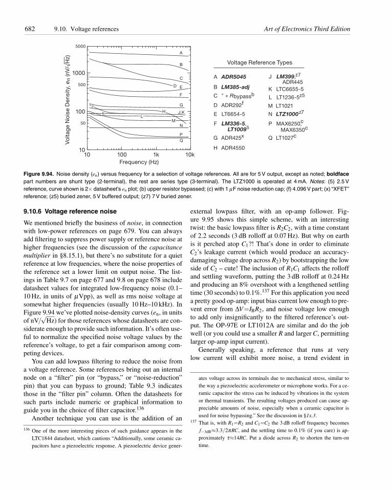
682 9.10. Voltage references Art of Electronics Third Edition
1010
100
1000
5000
500
50
100Frequency (Hz)
1k 10k
Vo
ltag
e N
ois
e D
ensi
ty, e
n (n
V/√H
z)
A
A
B
B
C
C
E
E
F
F
J
K
G
G
N
N
PQ
P
Q
L
L
M
MJ,K
J
K
H
H
D
D
ADR5045
LM385-adj
LT6654-5
Voltage Reference Types
LM336-5,
ADR425x
LTZ1000z7
MAX6350c
LT1027c
LT1236-5z5
LT1021
ADR445
LT10095
LTC6655-5
ADR4550
ADR292f" + Rbypassb
LM399,z7
MAX6250,c
Figure 9.94. Noise density (en) versus frequency for a selection of voltage references. All are for 5 V output, except as noted; boldfacepart numbers are shunt type (2-terminal), the rest are series type (3-terminal). The LTZ1000 is operated at 4 mA. Notes: (5) 2.5 Vreference, curve shown is 2× datasheet’s en plot; (b) upper resistor bypassed; (c) with 1 μF noise reduction cap; (f) 4.096 V part; (x) “XFET”reference; (z5) buried zener, 5 V buffered output; (z7) 7 V buried zener.
9.10.6 Voltage reference noise
We mentioned briefly the business of noise, in connectionwith low-power references on page 679. You can alwaysadd filtering to suppress power supply or reference noise athigher frequencies (see the discussion of the capacitancemultiplier in §8.15.1), but there’s no substitute for a quietreference at low frequencies, where the noise properties ofthe reference set a lower limit on output noise. The list-ings in Table 9.7 on page 677 and 9.8 on page 678 includedatasheet values for integrated low-frequency noise (0.1–10 Hz, in units of μVpp), as well as rms noise voltage atsomewhat higher frequencies (usually 10 Hz–10 kHz). InFigure 9.94 we’ve plotted noise-density curves (en, in unitsof nV/
√Hz) for those references whose datasheets are con-
siderate enough to provide such information. It’s often use-ful to normalize the specified noise voltage values by thereference’s voltage, to get a fair comparison among com-peting devices.
You can add lowpass filtering to reduce the noise froma voltage reference. Some references bring out an internalnode on a “filter” pin (or “bypass,” or “noise-reduction”pin) that you can bypass to ground; Table 9.3 indicatesthose in the “filter pin” column. Often the datasheets forsuch parts include numeric or graphical information toguide you in the choice of filter capacitor.136
Another technique you can use is the addition of an
136 One of the more interesting pieces of such guidance appears in theLTC1844 datasheet, which cautions “Additionally, some ceramic ca-pacitors have a piezoelectric response. A piezoelectric device gener-
external lowpass filter, with an op-amp follower. Fig-ure 9.95 shows this simple scheme, with an interestingtwist: the basic lowpass filter is R2C2, with a time constantof 2.2 seconds (3 dB rolloff at 0.07 Hz). But why on earthis it perched atop C1?! That’s done in order to eliminateC2’s leakage current (which would produce an accuracy-damaging voltage drop across R2) by bootstrapping the lowside of C2 – cute! The inclusion of R1C1 affects the rolloffand settling waveform, putting the 3 dB rolloff at 0.24 Hzand producing an 8% overshoot with a lengthened settlingtime (30 seconds) to 0.1%.137 For this application you needa pretty good op-amp: input bias current low enough to pre-vent error from ΔV=IBR2, and noise voltage low enoughto add only insignificantly to the filtered reference’s out-put. The OP-97E or LT1012A are similar and do the jobwell (or you could use a smaller R and larger C, permittinglarger op-amp input current).
Generally speaking, a reference that runs at verylow current will exhibit more noise, a trend evident in
ates voltage across its terminals due to mechanical stress, similar tothe way a piezoelectric accelerometer or microphone works. For a ce-ramic capacitor the stress can be induced by vibrations in the systemor thermal transients. The resulting voltages produced can cause ap-preciable amounts of noise, especially when a ceramic capacitor isused for noise bypassing.” See the discussion in §1x.3.
137 That is, with R1=R2 and C1=C2 the 3 dB rolloff frequency becomesf−3dB≈3.3/2πRC, and the settling time to 0.1% (if you care) is ap-proximately τ≈14RC. Put a diode across R2 to shorten the turn-ontime.
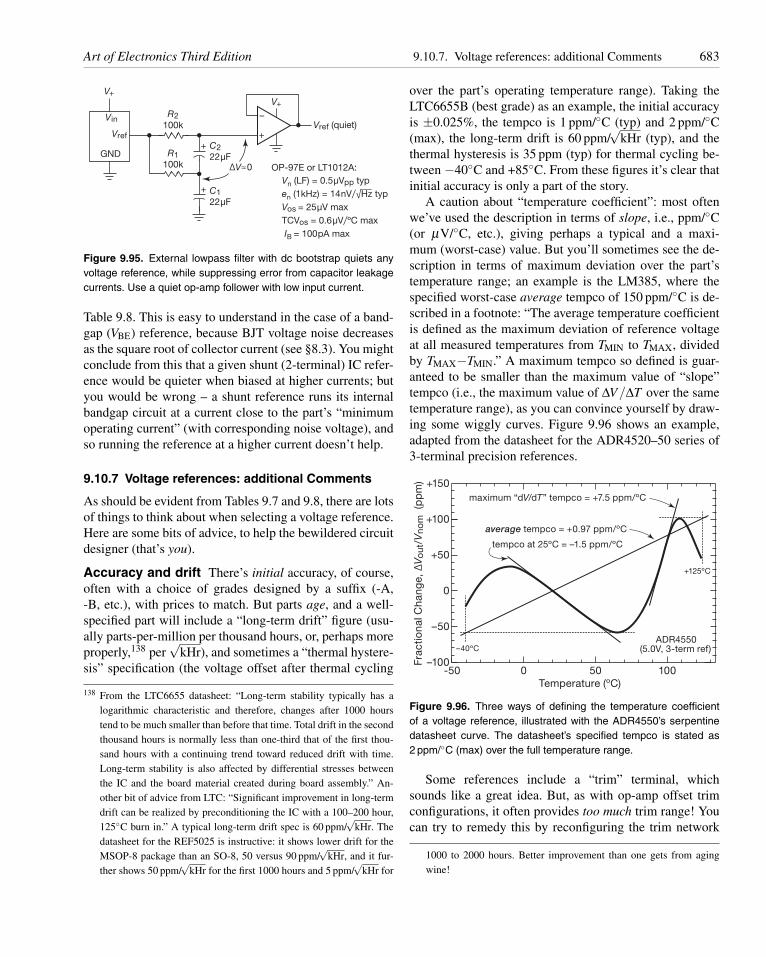
Art of Electronics Third Edition 9.10.7. Voltage references: additional Comments 683
++
+
–
GND
V+V+
VinR2
100k
R1
100k
C1
22μF
C2
22μFΔV≈0
Vref
Vref (quiet)
OP-97E or LT1012A:
Vn (LF) = 0.5μVpp typ
en (1kHz) = 14nV/√Hz typ
Vos = 25μV max
TCVos = 0.6μV/ºC max
IB = 100pA max
Figure 9.95. External lowpass filter with dc bootstrap quiets anyvoltage reference, while suppressing error from capacitor leakagecurrents. Use a quiet op-amp follower with low input current.
Table 9.8. This is easy to understand in the case of a band-gap (VBE) reference, because BJT voltage noise decreasesas the square root of collector current (see §8.3). You mightconclude from this that a given shunt (2-terminal) IC refer-ence would be quieter when biased at higher currents; butyou would be wrong – a shunt reference runs its internalbandgap circuit at a current close to the part’s “minimumoperating current” (with corresponding noise voltage), andso running the reference at a higher current doesn’t help.
9.10.7 Voltage references: additional Comments
As should be evident from Tables 9.7 and 9.8, there are lotsof things to think about when selecting a voltage reference.Here are some bits of advice, to help the bewildered circuitdesigner (that’s you).
Accuracy and drift There’s initial accuracy, of course,often with a choice of grades designed by a suffix (-A,-B, etc.), with prices to match. But parts age, and a well-specified part will include a “long-term drift” figure (usu-ally parts-per-million per thousand hours, or, perhaps moreproperly,138 per
√kHr), and sometimes a “thermal hystere-
sis” specification (the voltage offset after thermal cycling
138 From the LTC6655 datasheet: “Long-term stability typically has alogarithmic characteristic and therefore, changes after 1000 hourstend to be much smaller than before that time. Total drift in the secondthousand hours is normally less than one-third that of the first thou-sand hours with a continuing trend toward reduced drift with time.Long-term stability is also affected by differential stresses betweenthe IC and the board material created during board assembly.” An-other bit of advice from LTC: “Significant improvement in long-termdrift can be realized by preconditioning the IC with a 100–200 hour,125◦C burn in.” A typical long-term drift spec is 60 ppm/
√kHr. The
datasheet for the REF5025 is instructive: it shows lower drift for theMSOP-8 package than an SO-8, 50 versus 90 ppm/
√kHr, and it fur-
ther shows 50 ppm/√
kHr for the first 1000 hours and 5 ppm/√
kHr for
over the part’s operating temperature range). Taking theLTC6655B (best grade) as an example, the initial accuracyis ±0.025%, the tempco is 1 ppm/◦C (typ) and 2 ppm/◦C(max), the long-term drift is 60 ppm/
√kHr (typ), and the
thermal hysteresis is 35 ppm (typ) for thermal cycling be-tween −40◦C and +85◦C. From these figures it’s clear thatinitial accuracy is only a part of the story.
A caution about “temperature coefficient”: most oftenwe’ve used the description in terms of slope, i.e., ppm/◦C(or μV/◦C, etc.), giving perhaps a typical and a maxi-mum (worst-case) value. But you’ll sometimes see the de-scription in terms of maximum deviation over the part’stemperature range; an example is the LM385, where thespecified worst-case average tempco of 150 ppm/◦C is de-scribed in a footnote: “The average temperature coefficientis defined as the maximum deviation of reference voltageat all measured temperatures from TMIN to TMAX, dividedby TMAX−TMIN.” A maximum tempco so defined is guar-anteed to be smaller than the maximum value of “slope”tempco (i.e., the maximum value of ΔV/ΔT over the sametemperature range), as you can convince yourself by draw-ing some wiggly curves. Figure 9.96 shows an example,adapted from the datasheet for the ADR4520–50 series of3-terminal precision references.
–100
–50
0
+50
+100
+150
100500-50Temperature (ºC)
Frac
tiona
l Cha
nge,
ΔV o
ut/V
nom
(p
pm
)
average tempco = +0.97 ppm/ºC
maximum “dV/dT” tempco = +7.5 ppm/ºC
ADR4550–40ºC
+125ºC
(5.0V, 3-term ref)
tempco at 25ºC = –1.5 ppm/ºC
Figure 9.96. Three ways of defining the temperature coefficientof a voltage reference, illustrated with the ADR4550’s serpentinedatasheet curve. The datasheet’s specified tempco is stated as2 ppm/◦C (max) over the full temperature range.
Some references include a “trim” terminal, whichsounds like a great idea. But, as with op-amp offset trimconfigurations, it often provides too much trim range! Youcan try to remedy this by reconfiguring the trim network
1000 to 2000 hours. Better improvement than one gets from agingwine!
684 9.11. Commercial power-supply modules Art of Electronics Third Edition
to supply less current. But a caution: some parts requirethat the external trim circuitry exhibit a specified tempera-ture coefficient. Perhaps you’re better off, as with op-amps,simply by choosing a reference with a tighter spec; a refer-ence of better initial precision usually provides better temp-co as well.
Self-heating Voltage references are happiest when theyare only lightly loaded. If a reference IC is used to power aload, on-chip heating produces thermal gradients that canseriously degrade the part’s accuracy and drift. For suchapplications it’s best to buffer the output with an op-amp.Most good op-amps have lower noise and offset voltagesthan the voltage reference itself (you can do the calcula-tion!), so it does not degrade the reference voltage. Quitethe opposite, in fact, considering the degrading effect ofsubstantial load current with an unbuffered reference –that’s the whole point. And even middle-of-the-road op-amps have far lower tempcos of offset voltage than mostvoltage references (but use a precision op-amp for a preci-sion reference, as we did in Figure 9.90).
An op-amp buffer also provides an ideal opportunity toadd an RC noise filter; see §9.10.6, with its unusual filterconfiguration (Figure 9.95).
External influences As the footnote on the previouspage suggests, you can seriously degrade a precision ref-erence’s accuracy by physically stressing the package; thestability is also compromised by the gradual infiltration ofhumidity through the plastic package. Sometimes you’llsee improved specs for hermetically sealed package ver-sions: the LT1236LS8 is packaged in hermetic LCC, andoffers an improved drift specification relative to the plas-tic LT1236 version. And the most stable references are of-fered exclusively in hermetic metal packages to circumventthese problems: for example the LM399 (thermally stabi-lized buried zener reference) comes only in a TO-46 metalcan; it specifies an excellent long-term drift specificationof 8 ppm/
√kHr (typ). Pretty good – but handily outdone by
the LTZ1000 “Ultra Precision” shunt reference (also in ametal-hermetic package), with a spectacular 0.3 ppm/
√kHr
(typ)!A recent contribution to the gallery of badnesses is the
exposure of floating-gate references (§9.10.4) to ionizingradiation, most seriously in the form of airport luggage in-spection x-ray machines or PCB post-assembly x-ray in-spection. According to Intersil’s Application Note,139 by
139 Intersil App Note #1533, 23Feb2010, X-Ray Effects on Intersil FGAReferences, which explains “The floating gate capacitor is susceptibleto radiation degradation from various particles and photons in exces-
actual experiment at US airports the voltage shift for ninesamples of a 5.0 V floating-gate reference (ISL21009) af-ter six passes through carry-on x-ray machines averaged25 ppm (negative); this is small compared with the initialaccuracy of ±100 ppm, but in the same ballpark as thespecified long-term (1000 hour) drift and hysteresis specs(both 50 ppm, typ).
Line and load regulation You’ve got to worry aboutregulation against input-voltage variations (“line regula-tion”) for a voltage reference that is powered from unregu-lated dc, for example in a battery-powered application. Forsuch use, a reference isn’t suitable that boasts a worst-casetempco of 3 ppm/◦C, but whose output varies 200 ppm pervolt of input change (these are the specs of an entry in Ta-ble 9.8), though that reference would be fine if poweredfrom a reasonably regulated dc rail. For this reason we’velisted the worst-case line regulation for the references inTable 9.8 – these vary over nearly a 1000:1 range!
Load regulation matters also if you are using the refer-ence as a voltage regulator, i.e., to power a load that drawsa few milliamps, perhaps with load-current variation. Butwe discourage such use of a precision reference, becauseit produces on-chip heating and drifts; for that reason (andlack of space) we’ve not listed load regulation specifica-tions in the tables.
9.11 Commercial power-supply modules
Throughout the chapter we have described how to designyour own regulated power supply, implicitly assuming thatis the best thing to do. Only in the discussion of line-operated switching power supplies did we suggest that thebetter part of valor is to swallow your pride and buy a com-mercial power supply.140
As the economic realities of life would have it, however,the best approach is often to use one of the many commer-cial power supplies sold by companies such as Artesyn,Astec, Astrodyne, Acopian, Ault, Condor, CUI, Elpac,Globtek, Lambda, Omron, Panasonic, Phihong, Power-One, V-Infinity, and literally hundreds more. They offer
sive doses, as the electrons generated in the silicon dioxide are col-lected in the storage cell. Normal radiation from cosmic rays or radonwhich exist in small amounts on earth will not cause the FGA refer-ence voltage to drift appreciably for over 100 years. Artificial sourcesof radiation such as X-ray machines are capable of high enough dosesto cause output voltage shift. Note that Flash memory devices are alsosusceptible to X-ray radiation degradation, although to a lesser degreeas they are not precision analog devices.”
140 “Dude, this is a league game.”
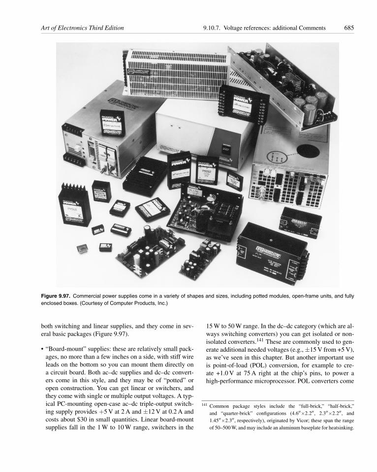
Art of Electronics Third Edition 9.10.7. Voltage references: additional Comments 685
Figure 9.97. Commercial power supplies come in a variety of shapes and sizes, including potted modules, open-frame units, and fullyenclosed boxes. (Courtesy of Computer Products, Inc.)
both switching and linear supplies, and they come in sev-eral basic packages (Figure 9.97).
• “Board-mount” supplies: these are relatively small pack-ages, no more than a few inches on a side, with stiff wireleads on the bottom so you can mount them directly ona circuit board. Both ac–dc supplies and dc–dc convert-ers come in this style, and they may be of “potted” oropen construction. You can get linear or switchers, andthey come with single or multiple output voltages. A typ-ical PC-mounting open-case ac–dc triple-output switch-ing supply provides +5 V at 2 A and ±12 V at 0.2 A andcosts about $30 in small quantities. Linear board-mountsupplies fall in the 1 W to 10 W range, switchers in the
15 W to 50 W range. In the dc–dc category (which are al-ways switching converters) you can get isolated or non-isolated converters.141 These are commonly used to gen-erate additional needed voltages (e.g., ±15 V from +5 V),as we’ve seen in this chapter. But another important useis point-of-load (POL) conversion, for example to cre-ate +1.0 V at 75 A right at the chip’s pins, to power ahigh-performance microprocessor. POL converters come
141 Common package styles include the “full-brick,” “half-brick,”and “quarter-brick” configurations (4.6′′×2.2′′, 2.3′′×2.2′′, and1.45′′×2.3′′, respectively), originated by Vicor; these span the rangeof 50–500 W, and may include an aluminum baseplate for heatsinking.
686 9.12. Energy storage: batteries and capacitors Art of Electronics Third Edition
in regulated and unregulated versions, the latter with afixed reduction ratio from a regulated dc input.142
• “Chassis-mount” supplies: these are larger power sup-plies, intended to be fastened to the inside of a largerinstrument. They come in both “open frame” and“enclosed-case” styles; the former have all the compo-nents on display, whereas the latter (for example, the“ATX” power supplies you find in a desktop or servercomputer) are wrapped in a perforated metal box. Theyare available in an enormous variety of voltages, both sin-gle and multiple outputs. Chassis-mount linear suppliesfall in the 10–200 W range, switchers in the 20–1500 Wrange.
• “External adapters”: these are the familiar black “wall-wart” and desktop (“desk-wart”?) that come with smallconsumer electronic gadgets, and which are widely avail-able from dozens of manufacturers. They actually comein three varieties, namely (a) step-down ac transformeronly, (b) unregulated dc supply, and (c) complete regu-lated dc supply; the latter can be either linear or switcher.Some of the switching units allow a full 95 to 252 Vacinput range, useful for traveling instruments.
• “DIN-rail mount” supplies: a popular way of mountingsome kinds of industrial electronics (relays, circuit break-ers, surge protectors, connectors, terminal blocks, and thelike) is the European-originated DIN rail, which consistsof a length of formed metal rail, 35 mm in width. Railmounting makes it easy to assemble electrical equipmentin industrial settings, and you can get a variety of switch-ing supplies in this style.
9.12 Energy storage: batteries and capacitors
No chapter dealing with regulators and power conversionwould be complete without a discussion of portable power.That usually means batteries (replaceable or rechargeable),
142 Although unregulated POLs might be expected to deliver poor “regu-lation,” in fact they can surprise you: for example, Vicor’s VTM seriesof high-efficiency fixed-ratio “current multipliers” (i.e., voltage step-down) include a unit rated at 130 A and 40:1 stepdown (thus 1.0 Vdcoutput from 40 Vdc input) with a worst-case output impedance of0.00094 Ω at 100◦C (thus < 0.1 V output change for a 100 A cur-rent step). Not bad. And you can always add feedback to the regulatedsupply that delivers the +40 Vdc input, to further stiffen the output forload change variations within the loop bandwidth. Moreover, theseconverters operate at 1.2 MHz switching frequency, so the residualripple is at 2.4 MHz, conveniently bypassed with relatively small fil-ter capacitors. In fact, the datasheet shows pretty good output-voltagewaveforms with 0–130 A load steps, exhibiting essentially no over-shoot even when the output is not filtered or bypassed with any exter-nal capacitor at all.
sometimes assisted by energy-storage capacitors. Contem-porary life is awash in portable electronic devices, whichhave driven the development and availability of improvedbatteries and capacitors. In this section we provide an in-troduction to battery choices and properties, and to the useof capacitors for energy storage. Because this chapter is al-ready, well, huge, we defer further discussion of the careand feeding of batteries to Chapter 9x in the advanced vol-ume.143
As we remarked in the previous edition, the (now out-of-print) Duracell “Comprehensive Battery Guide” listed133 off-the-shelf batteries, with descriptions like zinc-carbon, alkaline manganese, lithium, mercury, silver, zinc-air, and nickel-cadmium. There are even subclasses, for ex-ample Li/FeS2, Li/MnO2, Li/SO2, Li/SOCl2, and “lithiumsolid state.” And from other manufacturers you can getsealed lead-acid and gel-type batteries. For the truly ex-otic application you might even want to consider fuel cellsor radioactive thermal generators. What are all these bat-teries? How do you choose what’s best for your portablewidget?
The foregoing list divides into so-called primary andsecondary batteries. Primary batteries are designed for asingle discharge cycle only, i.e., they’re nonrechargeable.Secondary cells (lithium-ion, nickel metal-hydride, andsealed lead-acid gel-type), by comparison, are designed tobe recharged, typically from 200 to 1000 times. You usu-ally make your choice among battery types based on trade-offs among price, energy density, shelf life, constancy ofvoltage during discharge, peak current capability, temper-ature range, and availability. Once you’ve picked the rightbattery chemistry, you figure out which battery (or seriescombination of batteries) has enough energy content forthe job.
Fortunately, it’s pretty easy to eliminate most of the bat-teries in the catalogs, if you follow our first suggestion:Avoid hard-to-get batteries. Besides being hard to find,they’re usually not fresh. So it’s usually better to stick withthe varieties available at the drugstore, or perhaps photog-raphy store, even if it results in somewhat less than opti-mum design. We particularly recommend the use of com-monly available batteries in the design of any consumerelectronic device; as consumers ourselves, we shun thoseinexpensive marvels that use exotic and expensive batter-ies. (Remember those early smoke detectors that used an11.2 V mercury battery? They’re better forgotten. . . )
143 See also the expansive discussion in Chapter 14 of the previous editionof this book.
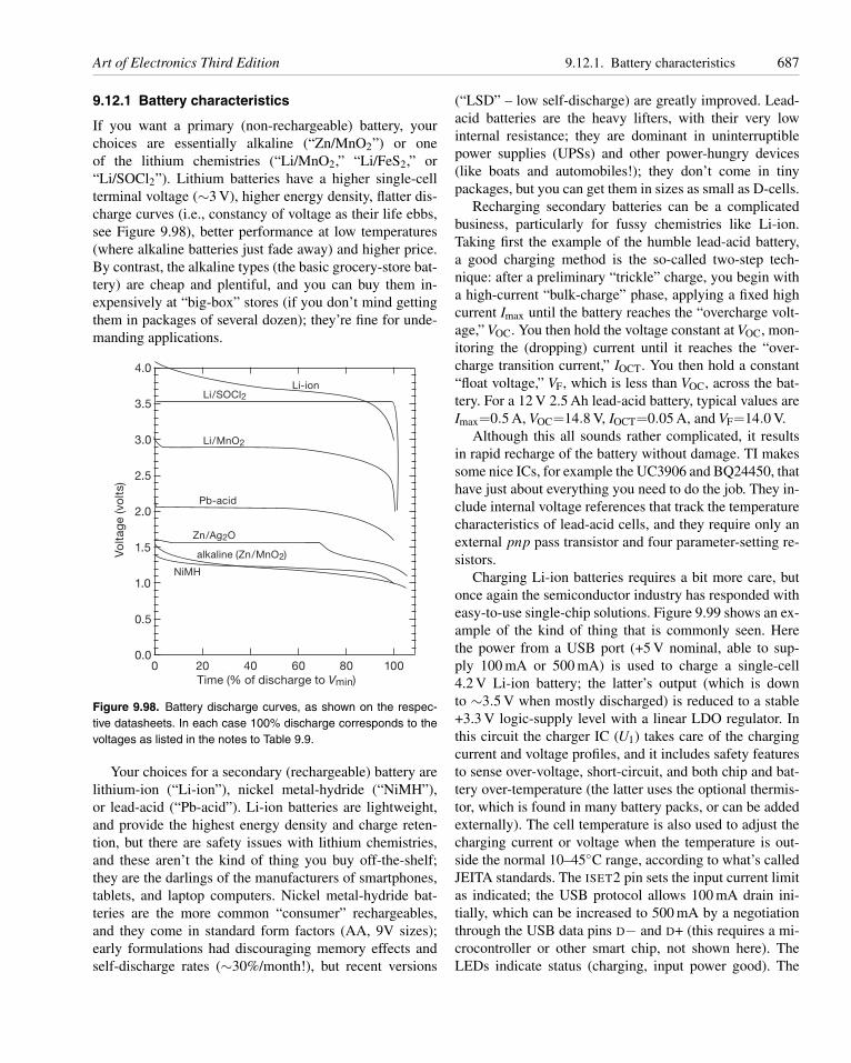
Art of Electronics Third Edition 9.12.1. Battery characteristics 687
9.12.1 Battery characteristics
If you want a primary (non-rechargeable) battery, yourchoices are essentially alkaline (“Zn/MnO2”) or oneof the lithium chemistries (“Li/MnO2,” “Li/FeS2,” or“Li/SOCl2”). Lithium batteries have a higher single-cellterminal voltage (∼3 V), higher energy density, flatter dis-charge curves (i.e., constancy of voltage as their life ebbs,see Figure 9.98), better performance at low temperatures(where alkaline batteries just fade away) and higher price.By contrast, the alkaline types (the basic grocery-store bat-tery) are cheap and plentiful, and you can buy them in-expensively at “big-box” stores (if you don’t mind gettingthem in packages of several dozen); they’re fine for unde-manding applications.
4.0
3.5
3.0
2.5
2.0
1.5
1.0
0.5
0.010080604020
Time (% of discharge to Vmin)
Vo
ltag
e (v
olts
)
0
NiMH
alkaline (Zn/MnO2)
Pb-acid
Zn/Ag2O
Li/MnO2
Li/SOCl2Li-ion
Figure 9.98. Battery discharge curves, as shown on the respec-tive datasheets. In each case 100% discharge corresponds to thevoltages as listed in the notes to Table 9.9.
Your choices for a secondary (rechargeable) battery arelithium-ion (“Li-ion”), nickel metal-hydride (“NiMH”),or lead-acid (“Pb-acid”). Li-ion batteries are lightweight,and provide the highest energy density and charge reten-tion, but there are safety issues with lithium chemistries,and these aren’t the kind of thing you buy off-the-shelf;they are the darlings of the manufacturers of smartphones,tablets, and laptop computers. Nickel metal-hydride bat-teries are the more common “consumer” rechargeables,and they come in standard form factors (AA, 9V sizes);early formulations had discouraging memory effects andself-discharge rates (∼30%/month!), but recent versions
(“LSD” – low self-discharge) are greatly improved. Lead-acid batteries are the heavy lifters, with their very lowinternal resistance; they are dominant in uninterruptiblepower supplies (UPSs) and other power-hungry devices(like boats and automobiles!); they don’t come in tinypackages, but you can get them in sizes as small as D-cells.
Recharging secondary batteries can be a complicatedbusiness, particularly for fussy chemistries like Li-ion.Taking first the example of the humble lead-acid battery,a good charging method is the so-called two-step tech-nique: after a preliminary “trickle” charge, you begin witha high-current “bulk-charge” phase, applying a fixed highcurrent Imax until the battery reaches the “overcharge volt-age,” VOC. You then hold the voltage constant at VOC, mon-itoring the (dropping) current until it reaches the “over-charge transition current,” IOCT. You then hold a constant“float voltage,” VF, which is less than VOC, across the bat-tery. For a 12 V 2.5 Ah lead-acid battery, typical values areImax=0.5 A, VOC=14.8 V, IOCT=0.05 A, and VF=14.0 V.
Although this all sounds rather complicated, it resultsin rapid recharge of the battery without damage. TI makessome nice ICs, for example the UC3906 and BQ24450, thathave just about everything you need to do the job. They in-clude internal voltage references that track the temperaturecharacteristics of lead-acid cells, and they require only anexternal pnp pass transistor and four parameter-setting re-sistors.
Charging Li-ion batteries requires a bit more care, butonce again the semiconductor industry has responded witheasy-to-use single-chip solutions. Figure 9.99 shows an ex-ample of the kind of thing that is commonly seen. Herethe power from a USB port (+5 V nominal, able to sup-ply 100 mA or 500 mA) is used to charge a single-cell4.2 V Li-ion battery; the latter’s output (which is downto ∼3.5 V when mostly discharged) is reduced to a stable+3.3 V logic-supply level with a linear LDO regulator. Inthis circuit the charger IC (U1) takes care of the chargingcurrent and voltage profiles, and it includes safety featuresto sense over-voltage, short-circuit, and both chip and bat-tery over-temperature (the latter uses the optional thermis-tor, which is found in many battery packs, or can be addedexternally). The cell temperature is also used to adjust thecharging current or voltage when the temperature is out-side the normal 10–45◦C range, according to what’s calledJEITA standards. The ISET2 pin sets the input current limitas indicated; the USB protocol allows 100 mA drain ini-tially, which can be increased to 500 mA by a negotiationthrough the USB data pins D− and D+ (this requires a mi-crocontroller or other smart chip, not shown here). TheLEDs indicate status (charging, input power good). The
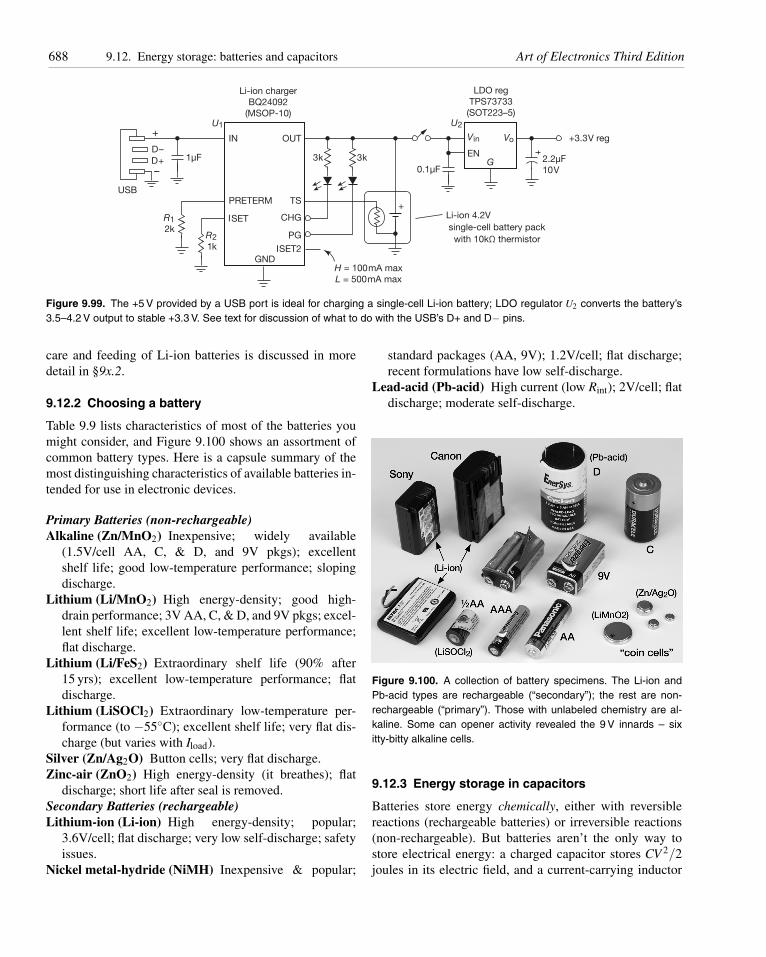
688 9.12. Energy storage: batteries and capacitors Art of Electronics Third Edition
Li-ion charger
BQ24092
(MSOP-10)
LDO reg
TPS73733
(SOT223–5)
Li-ion 4.2V
single-cell battery pack
with 10kΩ thermistor
H = 100mA max
L = 500mA max
U1 U2
ENG
IN
PRETERM
SET
USB
1μF 2.2μF
10V
+3.3V reg
D–
D+
+
–
OUT
TS
CHG
PG
SET2GND
0.1μF
R1
2kR2
1k
3k 3k
+
Vin Vo
I
I
Figure 9.99. The +5 V provided by a USB port is ideal for charging a single-cell Li-ion battery; LDO regulator U2 converts the battery’s3.5–4.2 V output to stable +3.3 V. See text for discussion of what to do with the USB’s D+ and D− pins.
care and feeding of Li-ion batteries is discussed in moredetail in §9x.2.
9.12.2 Choosing a battery
Table 9.9 lists characteristics of most of the batteries youmight consider, and Figure 9.100 shows an assortment ofcommon battery types. Here is a capsule summary of themost distinguishing characteristics of available batteries in-tended for use in electronic devices.
Primary Batteries (non-rechargeable)Alkaline (Zn/MnO2) Inexpensive; widely available
(1.5V/cell AA, C, & D, and 9V pkgs); excellentshelf life; good low-temperature performance; slopingdischarge.
Lithium (Li/MnO2) High energy-density; good high-drain performance; 3V AA, C, & D, and 9V pkgs; excel-lent shelf life; excellent low-temperature performance;flat discharge.
Lithium (Li/FeS2) Extraordinary shelf life (90% after15 yrs); excellent low-temperature performance; flatdischarge.
Lithium (LiSOCl2) Extraordinary low-temperature per-formance (to −55◦C); excellent shelf life; very flat dis-charge (but varies with Iload).
Silver (Zn/Ag2O) Button cells; very flat discharge.Zinc-air (ZnO2) High energy-density (it breathes); flat
discharge; short life after seal is removed.Secondary Batteries (rechargeable)Lithium-ion (Li-ion) High energy-density; popular;
3.6V/cell; flat discharge; very low self-discharge; safetyissues.
Nickel metal-hydride (NiMH) Inexpensive & popular;
standard packages (AA, 9V); 1.2V/cell; flat discharge;recent formulations have low self-discharge.
Lead-acid (Pb-acid) High current (low Rint); 2V/cell; flatdischarge; moderate self-discharge.
Figure 9.100. A collection of battery specimens. The Li-ion andPb-acid types are rechargeable (“secondary”); the rest are non-rechargeable (“primary”). Those with unlabeled chemistry are al-kaline. Some can opener activity revealed the 9 V innards – sixitty-bitty alkaline cells.
9.12.3 Energy storage in capacitors
Batteries store energy chemically, either with reversiblereactions (rechargeable batteries) or irreversible reactions(non-rechargeable). But batteries aren’t the only way tostore electrical energy: a charged capacitor stores CV 2/2joules in its electric field, and a current-carrying inductor
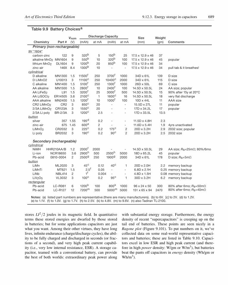
Art of Electronics Third Edition 9.12.3. Energy storage in capacitors 689
cylindrical
button
Li poly BR2032 2.5
cylindricalNiMH HHR210AA/B 2000 - 14.5D x 50.5L AA size; Rs=25mΩ; 80%/6mo
button
rectangularPb-acid LC-R061 800k 96 x 24 x 50 300
Pb-acid
Notes: (a) listed part numbers are representative (there are many manufacturers). (b) to 6V. [c] to 2V. (d) to 1.2V.(e) to 1.1V. (f) to 1.0V. (g) to 1.7V. (h) to 2.5V. (k) to 4.8V. (m) to 9.6V. (n) also Tadiran TL-2100.
VnomDischarge Capacity
Size Weight
Chemistry
Table 9.9 Battery Choicesa
Part # (V) (mAh) at mA (mAh) at mA (mm) (gm) Comments
Primary (non-rechargeable)9V "1604"
carbon-zinc 122 9 320b 5 150b 25 17.5 x 12.9 x 46 37
alkaline MnO2 MN1604 9 550b 10
10
320b 100 17.5 x 12.9 x 46 45
lithium MnO2 DL1604 9 1200b 20 850b 100 17.5 x 12.9 x 46 34
zinc-air 146X 8.4 - 17.5 x 12.9 x 46 34
178
29
D alkaline MN1300 1.5 11500f 250 3700f 1000 34D x 61L 139 D size
D LiMnO2 U10013 3 11100c 250 10400c 2000 34D x 61L 115 D size
C alkaline MN1400 1.5 5100f 250
100
1300f 1000
1000
26D x 50L 69 C size
AA alkaline MN1500 1.5 2800f 10 2400f 100 14.5D x 50.5L 24 AA size; popular
AA LiFeS2 L91 1.5 3200f 25 3000f 500 14.5D x 50.5L 15 90% after 15y at 20ºC
AA LiSOCl2 ER14505 3.6 2100c 1 1600c
1900g
16 14.5D x 50.5L 18 very flat discharge
AAA alkaline MN2400 1.5 1200f 10 1000f 100 10D x 44L 11 AAA size
CR2 LiMnO2 CR2 3 850c 20 - -
-
15.5D x 27L 11
2/3A LiMnO2 CR123A 3 1550c 20
3 1200c 2.5
- - 17D x 34.2L 17
- 17D x 33.5L 13.52/3A Li poly BR-2/3A -
silver 357 1.55 195d 0.2 - - 11.5D x 4.8H 2.3
zinc-air 675 1.45 600e 2 - - 11.6D x 5.4H 1.9 4yrs unactivated
LiMnO2 CR2032 3 225c
3
1.2
2
190c0.2
0.2
175c 2 20D x 3.2H
90c 2 20D x 3.2H
2.9 2032 size; popular
2032 size
Secondary (rechargeable)
Pb-acid 0810-0004 250 2000
LiMn ML2020 3 45c 0.12 40c 1 20D x 2.0H 2.2
LiMnTi MT621 1.5 2.5f
2 1f0.05 - -
-
6.8D x 2.1H 0.25
- 4.8D x 1.5H 0.08LiNb NBL414 0.004 -
LiV2O5 VL3032 3 100c
6 1200k
LC-R127 5000m 151 x 65 x 94 2470500 500012 7200m
2000f
2500g
0.2 95c 1 30D x 3.2H 6.2
80% after 6mo; Rs=50mΩ
80% after 6mo; Rs=40mΩ
D size; Rs=5mΩ34D x 61L
1300b
452500h3.6Li-ion NCR18650 500 50002900h popular
memory backup
memory backup
memory backup
memory backup
popular
popular
pull tab & it breathes!
popular
18D x 65.2L
stores LI2/2 joules in its magnetic field. In quantitativeterms these stored energies are dwarfed by those storedin batteries; but for some applications capacitors are justwhat you want. Among their other virtues, they have longlives, infinite endurance (charge/discharge cycles), the abil-ity to be fully charged and discharged in seconds (or frac-tions of a second), and very high peak current capabil-ity (i.e., very low internal resistance, ESR). A storage ca-pacitor, teamed with a conventional battery, can providethe best of both worlds: extraordinary peak power along
with substantial energy storage. Furthermore, the energydensity of recent “supercapacitors” is creeping up on thetail end of batteries. These points are seen nicely in aRagone plot (Figure 9.101). To put numbers on it, we’vecollected data on some real-world representative capaci-tors and batteries; these are listed in Table 9.10. Capaci-tors excel in low ESR and high peak current (and there-fore in high power density: W/gm or W/m3), but batteriesbeat the pants off capacitors in energy density (Wh/gm orWh/m3).
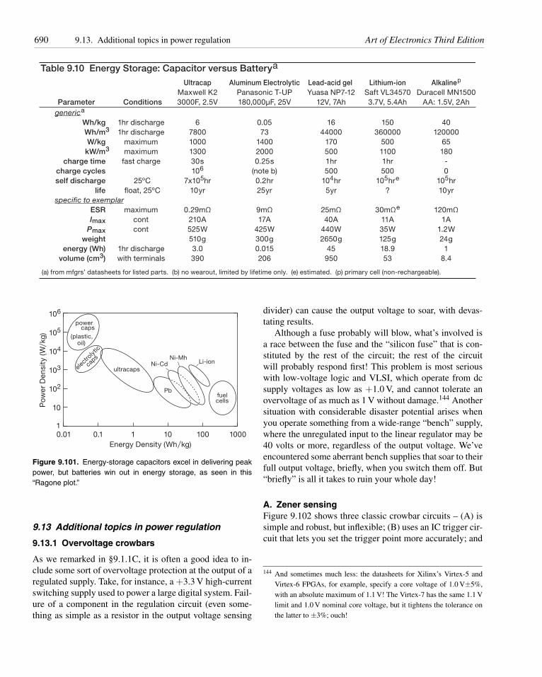
690 9.13. Additional topics in power regulation Art of Electronics Third Edition
Table 9.10 Energy Storage: Capacitor versus Batterya
Ultracap Aluminum Electrolytic Lead-acid gel Lithium-ion Alkalinep
Maxwell K2 Panasonic T-UP Yuasa NP7-12 Saft VL34570 Duracell MN1500
Parameter Conditions 3000F, 2.5V 180,000μF, 25V 12V, 7Ah 3.7V, 5.4Ah AA: 1.5V, 2Ah
generica
Wh/kg 1hr discharge 6 0.05 16 150 40
Wh/m3 1hr discharge 7800 73 44000 360000 120000
W/kg maximum 1000 1400 170 500 65
kW/m3 maximum 1300 2000 500 1100 180
charge time fast charge 30s 0.25s 1hr 1hr -
charge cycles 106 (note b) 500 500 0
self discharge 25ºC 7x10⁵hr 0.2hr 104hr 105hre 105hr
life float, 25ºC 10yr 10yr25yr 5yr ?
specific to exemplarESR maximum 0.29mΩ 9mΩ 25mΩ 30mΩe 120mΩ
Imax cont 210A 17A 40A 11A 1A
Pmax cont 525W 425W 440W 35W 1.2W
weight 510g 300g 2650g 125g 24g
energy (Wh) 1hr discharge 3.0 0.015 45 18.9 1
volume (cm3) with terminals 390 206 950 53 8.4
(a) from mfgrs’ datasheets for listed parts. (b) no wearout, limited by lifetime only. (e) estimated. (p) primary cell (non-rechargeable).
0.01
Energy Density (Wh/kg)
Po
we
r D
en
sit
y (
W/k
g)
0.1 11
10
10
104
105
102
103
106
100 1000
power
elec
troly
tic
caps
caps
ultracaps
fuelPb
Ni-CdNi-Mh
Li-ion
cells
oil)(plastic,
Figure 9.101. Energy-storage capacitors excel in delivering peakpower, but batteries win out in energy storage, as seen in this“Ragone plot.”
9.13 Additional topics in power regulation
9.13.1 Overvoltage crowbars
As we remarked in §9.1.1C, it is often a good idea to in-clude some sort of overvoltage protection at the output of aregulated supply. Take, for instance, a +3.3 V high-currentswitching supply used to power a large digital system. Fail-ure of a component in the regulation circuit (even some-thing as simple as a resistor in the output voltage sensing
divider) can cause the output voltage to soar, with devas-tating results.
Although a fuse probably will blow, what’s involved isa race between the fuse and the “silicon fuse” that is con-stituted by the rest of the circuit; the rest of the circuitwill probably respond first! This problem is most seriouswith low-voltage logic and VLSI, which operate from dcsupply voltages as low as +1.0 V, and cannot tolerate anovervoltage of as much as 1 V without damage.144 Anothersituation with considerable disaster potential arises whenyou operate something from a wide-range “bench” supply,where the unregulated input to the linear regulator may be40 volts or more, regardless of the output voltage. We’veencountered some aberrant bench supplies that soar to theirfull output voltage, briefly, when you switch them off. But“briefly” is all it takes to ruin your whole day!
A. Zener sensingFigure 9.102 shows three classic crowbar circuits – (A) issimple and robust, but inflexible; (B) uses an IC trigger cir-cuit that lets you set the trigger point more accurately; and
144 And sometimes much less: the datasheets for Xilinx’s Virtex-5 andVirtex-6 FPGAs, for example, specify a core voltage of 1.0 V±5%,with an absolute maximum of 1.1 V! The Virtex-7 has the same 1.1 Vlimit and 1.0 V nominal core voltage, but it tightens the tolerance onthe latter to ±3%; ouch!
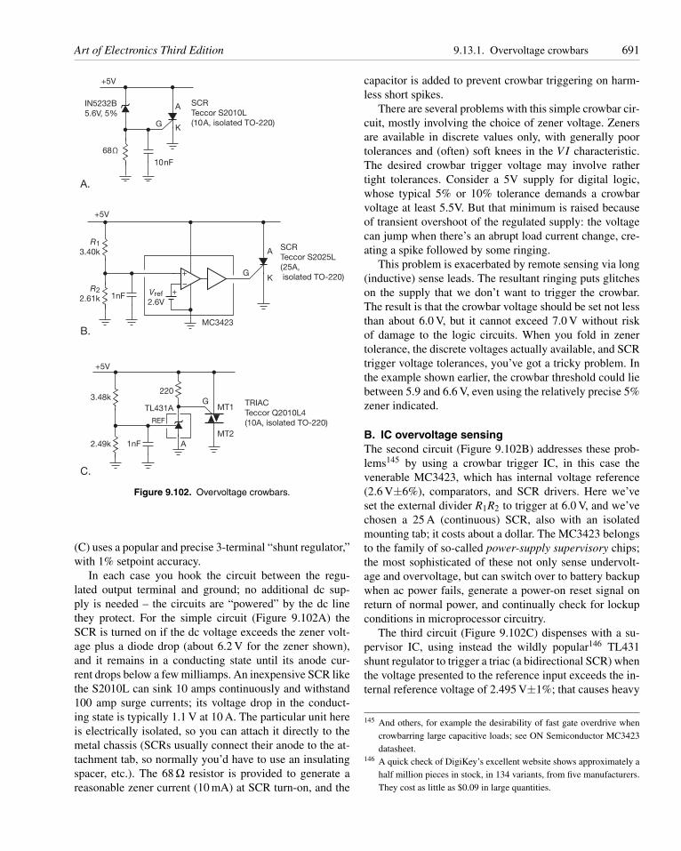
Art of Electronics Third Edition 9.13.1. Overvoltage crowbars 691
+5V
+5V
+5V
3.48k
2.49k
A.
B.
C.
10nF
1nF
1nF
220
TL431A
REF
MT1
MT2
MC3423
SCR
Teccor S2010L
(10A, isolated TO-220)
SCR
Teccor S2025L
(25A,
isolated TO-220)
TRIAC
Teccor Q2010L4
(10A, isolated TO-220)
G
G
G
A
A
A
K
K
R1
3.40k
Vref
2.6V
R2
2.61k
IN5232B
5.6V, 5%
68Ω
+
+–
Figure 9.102. Overvoltage crowbars.
(C) uses a popular and precise 3-terminal “shunt regulator,”with 1% setpoint accuracy.
In each case you hook the circuit between the regu-lated output terminal and ground; no additional dc sup-ply is needed – the circuits are “powered” by the dc linethey protect. For the simple circuit (Figure 9.102A) theSCR is turned on if the dc voltage exceeds the zener volt-age plus a diode drop (about 6.2 V for the zener shown),and it remains in a conducting state until its anode cur-rent drops below a few milliamps. An inexpensive SCR likethe S2010L can sink 10 amps continuously and withstand100 amp surge currents; its voltage drop in the conduct-ing state is typically 1.1 V at 10 A. The particular unit hereis electrically isolated, so you can attach it directly to themetal chassis (SCRs usually connect their anode to the at-tachment tab, so normally you’d have to use an insulatingspacer, etc.). The 68 Ω resistor is provided to generate areasonable zener current (10 mA) at SCR turn-on, and the
capacitor is added to prevent crowbar triggering on harm-less short spikes.
There are several problems with this simple crowbar cir-cuit, mostly involving the choice of zener voltage. Zenersare available in discrete values only, with generally poortolerances and (often) soft knees in the V I characteristic.The desired crowbar trigger voltage may involve rathertight tolerances. Consider a 5V supply for digital logic,whose typical 5% or 10% tolerance demands a crowbarvoltage at least 5.5V. But that minimum is raised becauseof transient overshoot of the regulated supply: the voltagecan jump when there’s an abrupt load current change, cre-ating a spike followed by some ringing.
This problem is exacerbated by remote sensing via long(inductive) sense leads. The resultant ringing puts glitcheson the supply that we don’t want to trigger the crowbar.The result is that the crowbar voltage should be set not lessthan about 6.0 V, but it cannot exceed 7.0 V without riskof damage to the logic circuits. When you fold in zenertolerance, the discrete voltages actually available, and SCRtrigger voltage tolerances, you’ve got a tricky problem. Inthe example shown earlier, the crowbar threshold could liebetween 5.9 and 6.6 V, even using the relatively precise 5%zener indicated.
B. IC overvoltage sensingThe second circuit (Figure 9.102B) addresses these prob-lems145 by using a crowbar trigger IC, in this case thevenerable MC3423, which has internal voltage reference(2.6 V±6%), comparators, and SCR drivers. Here we’veset the external divider R1R2 to trigger at 6.0 V, and we’vechosen a 25 A (continuous) SCR, also with an isolatedmounting tab; it costs about a dollar. The MC3423 belongsto the family of so-called power-supply supervisory chips;the most sophisticated of these not only sense undervolt-age and overvoltage, but can switch over to battery backupwhen ac power fails, generate a power-on reset signal onreturn of normal power, and continually check for lockupconditions in microprocessor circuitry.
The third circuit (Figure 9.102C) dispenses with a su-pervisor IC, using instead the wildly popular146 TL431shunt regulator to trigger a triac (a bidirectional SCR) whenthe voltage presented to the reference input exceeds the in-ternal reference voltage of 2.495 V±1%; that causes heavy
145 And others, for example the desirability of fast gate overdrive whencrowbarring large capacitive loads; see ON Semiconductor MC3423datasheet.
146 A quick check of DigiKey’s excellent website shows approximately ahalf million pieces in stock, in 134 variants, from five manufacturers.They cost as little as $0.09 in large quantities.
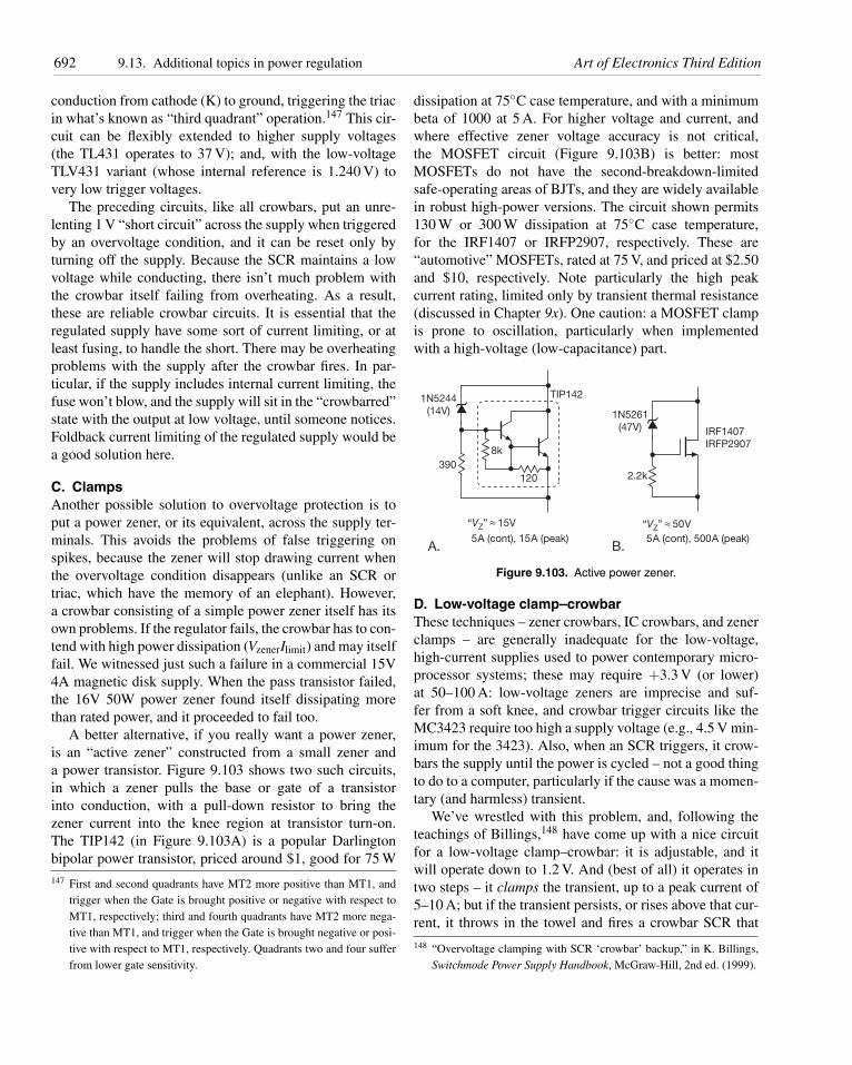
692 9.13. Additional topics in power regulation Art of Electronics Third Edition
conduction from cathode (K) to ground, triggering the triacin what’s known as “third quadrant” operation.147 This cir-cuit can be flexibly extended to higher supply voltages(the TL431 operates to 37 V); and, with the low-voltageTLV431 variant (whose internal reference is 1.240 V) tovery low trigger voltages.
The preceding circuits, like all crowbars, put an unre-lenting 1 V “short circuit” across the supply when triggeredby an overvoltage condition, and it can be reset only byturning off the supply. Because the SCR maintains a lowvoltage while conducting, there isn’t much problem withthe crowbar itself failing from overheating. As a result,these are reliable crowbar circuits. It is essential that theregulated supply have some sort of current limiting, or atleast fusing, to handle the short. There may be overheatingproblems with the supply after the crowbar fires. In par-ticular, if the supply includes internal current limiting, thefuse won’t blow, and the supply will sit in the “crowbarred”state with the output at low voltage, until someone notices.Foldback current limiting of the regulated supply would bea good solution here.
C. ClampsAnother possible solution to overvoltage protection is toput a power zener, or its equivalent, across the supply ter-minals. This avoids the problems of false triggering onspikes, because the zener will stop drawing current whenthe overvoltage condition disappears (unlike an SCR ortriac, which have the memory of an elephant). However,a crowbar consisting of a simple power zener itself has itsown problems. If the regulator fails, the crowbar has to con-tend with high power dissipation (VzenerIlimit) and may itselffail. We witnessed just such a failure in a commercial 15V4A magnetic disk supply. When the pass transistor failed,the 16V 50W power zener found itself dissipating morethan rated power, and it proceeded to fail too.
A better alternative, if you really want a power zener,is an “active zener” constructed from a small zener anda power transistor. Figure 9.103 shows two such circuits,in which a zener pulls the base or gate of a transistorinto conduction, with a pull-down resistor to bring thezener current into the knee region at transistor turn-on.The TIP142 (in Figure 9.103A) is a popular Darlingtonbipolar power transistor, priced around $1, good for 75 W147 First and second quadrants have MT2 more positive than MT1, and
trigger when the Gate is brought positive or negative with respect toMT1, respectively; third and fourth quadrants have MT2 more nega-tive than MT1, and trigger when the Gate is brought negative or posi-tive with respect to MT1, respectively. Quadrants two and four sufferfrom lower gate sensitivity.
dissipation at 75◦C case temperature, and with a minimumbeta of 1000 at 5 A. For higher voltage and current, andwhere effective zener voltage accuracy is not critical,the MOSFET circuit (Figure 9.103B) is better: mostMOSFETs do not have the second-breakdown-limitedsafe-operating areas of BJTs, and they are widely availablein robust high-power versions. The circuit shown permits130 W or 300 W dissipation at 75◦C case temperature,for the IRF1407 or IRFP2907, respectively. These are“automotive” MOSFETs, rated at 75 V, and priced at $2.50and $10, respectively. Note particularly the high peakcurrent rating, limited only by transient thermal resistance(discussed in Chapter 9x). One caution: a MOSFET clampis prone to oscillation, particularly when implementedwith a high-voltage (low-capacitance) part.
8k
120
390
A. B.
TIP142
IRF1407
IRFP2907
2.2k
1N5244
(14V) 1N5261
(47V)
5A (cont), 15A (peak)
“VZ” ≈ 15V
5A (cont), 500A (peak)
“VZ” ≈ 50V
Figure 9.103. Active power zener.
D. Low-voltage clamp–crowbarThese techniques – zener crowbars, IC crowbars, and zenerclamps – are generally inadequate for the low-voltage,high-current supplies used to power contemporary micro-processor systems; these may require +3.3 V (or lower)at 50–100 A: low-voltage zeners are imprecise and suf-fer from a soft knee, and crowbar trigger circuits like theMC3423 require too high a supply voltage (e.g., 4.5 V min-imum for the 3423). Also, when an SCR triggers, it crow-bars the supply until the power is cycled – not a good thingto do to a computer, particularly if the cause was a momen-tary (and harmless) transient.
We’ve wrestled with this problem, and, following theteachings of Billings,148 have come up with a nice circuitfor a low-voltage clamp–crowbar: it is adjustable, and itwill operate down to 1.2 V. And (best of all) it operates intwo steps – it clamps the transient, up to a peak current of5–10 A; but if the transient persists, or rises above that cur-rent, it throws in the towel and fires a crowbar SCR that
148 “Overvoltage clamping with SCR ‘crowbar’ backup,” in K. Billings,Switchmode Power Supply Handbook, McGraw-Hill, 2nd ed. (1999).
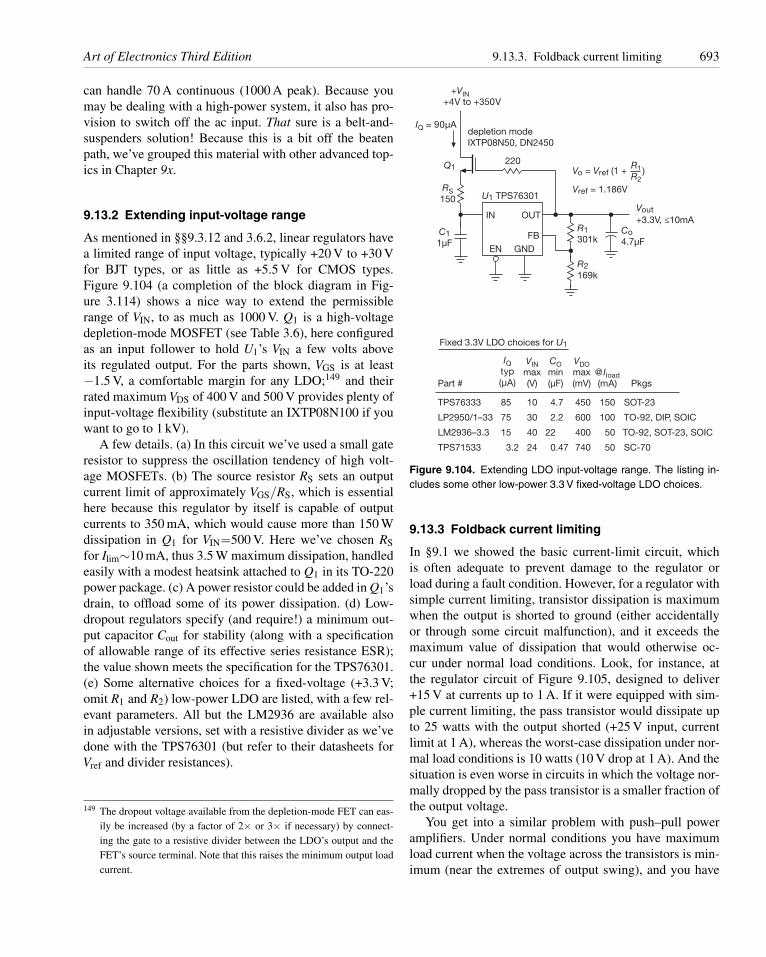
Art of Electronics Third Edition 9.13.3. Foldback current limiting 693
can handle 70 A continuous (1000 A peak). Because youmay be dealing with a high-power system, it also has pro-vision to switch off the ac input. That sure is a belt-and-suspenders solution! Because this is a bit off the beatenpath, we’ve grouped this material with other advanced top-ics in Chapter 9x.
9.13.2 Extending input-voltage range
As mentioned in §§9.3.12 and 3.6.2, linear regulators havea limited range of input voltage, typically +20 V to +30 Vfor BJT types, or as little as +5.5 V for CMOS types.Figure 9.104 (a completion of the block diagram in Fig-ure 3.114) shows a nice way to extend the permissiblerange of VIN, to as much as 1000 V. Q1 is a high-voltagedepletion-mode MOSFET (see Table 3.6), here configuredas an input follower to hold U1’s VIN a few volts aboveits regulated output. For the parts shown, VGS is at least−1.5 V, a comfortable margin for any LDO;149 and theirrated maximum VDS of 400 V and 500 V provides plenty ofinput-voltage flexibility (substitute an IXTP08N100 if youwant to go to 1 kV).
A few details. (a) In this circuit we’ve used a small gateresistor to suppress the oscillation tendency of high volt-age MOSFETs. (b) The source resistor RS sets an outputcurrent limit of approximately VGS/RS, which is essentialhere because this regulator by itself is capable of outputcurrents to 350 mA, which would cause more than 150 Wdissipation in Q1 for VIN=500 V. Here we’ve chosen RS
for Ilim∼10 mA, thus 3.5 W maximum dissipation, handledeasily with a modest heatsink attached to Q1 in its TO-220power package. (c) A power resistor could be added in Q1’sdrain, to offload some of its power dissipation. (d) Low-dropout regulators specify (and require!) a minimum out-put capacitor Cout for stability (along with a specificationof allowable range of its effective series resistance ESR);the value shown meets the specification for the TPS76301.(e) Some alternative choices for a fixed-voltage (+3.3 V;omit R1 and R2) low-power LDO are listed, with a few rel-evant parameters. All but the LM2936 are available alsoin adjustable versions, set with a resistive divider as we’vedone with the TPS76301 (but refer to their datasheets forVref and divider resistances).
149 The dropout voltage available from the depletion-mode FET can eas-ily be increased (by a factor of 2× or 3× if necessary) by connect-ing the gate to a resistive divider between the LDO’s output and theFET’s source terminal. Note that this raises the minimum output loadcurrent.
+VIN
+4V to +350V
RS
150
depletion mode
IXTP08N50, DN2450
Fixed 3.3V LDO choices for U1
220
U1 TPS76301
IN
EN GND
FB
OUT
Q1
C1
1μF
Vref = 1.186V
Vo = Vref (1 + )R1
R2
Vout
+3.3V, ≤10mAR1
301k
R2
169k
Co
4.7μF
IQ = 90μA
IQtyp
(μA)@ Iload
(mA)
VIN
max
(V)
VDO
max
(mV) PkgsPart #
TPS76333 85 10 4.7 450 150 SOT-23
LP2950/1–33 75 30 2.2 600 100 TO-92, DIP, SOIC
LM2936–3.3 15 40 22 400 50 TO-92, SOT-23, SOIC
TPS71533 3.2 24 0.47 740 50 SC-70
CO
min
(μF)
Figure 9.104. Extending LDO input-voltage range. The listing in-cludes some other low-power 3.3 V fixed-voltage LDO choices.
9.13.3 Foldback current limiting
In §9.1 we showed the basic current-limit circuit, whichis often adequate to prevent damage to the regulator orload during a fault condition. However, for a regulator withsimple current limiting, transistor dissipation is maximumwhen the output is shorted to ground (either accidentallyor through some circuit malfunction), and it exceeds themaximum value of dissipation that would otherwise oc-cur under normal load conditions. Look, for instance, atthe regulator circuit of Figure 9.105, designed to deliver+15 V at currents up to 1 A. If it were equipped with sim-ple current limiting, the pass transistor would dissipate upto 25 watts with the output shorted (+25 V input, currentlimit at 1 A), whereas the worst-case dissipation under nor-mal load conditions is 10 watts (10 V drop at 1 A). And thesituation is even worse in circuits in which the voltage nor-mally dropped by the pass transistor is a smaller fraction ofthe output voltage.
You get into a similar problem with push–pull poweramplifiers. Under normal conditions you have maximumload current when the voltage across the transistors is min-imum (near the extremes of output swing), and you have
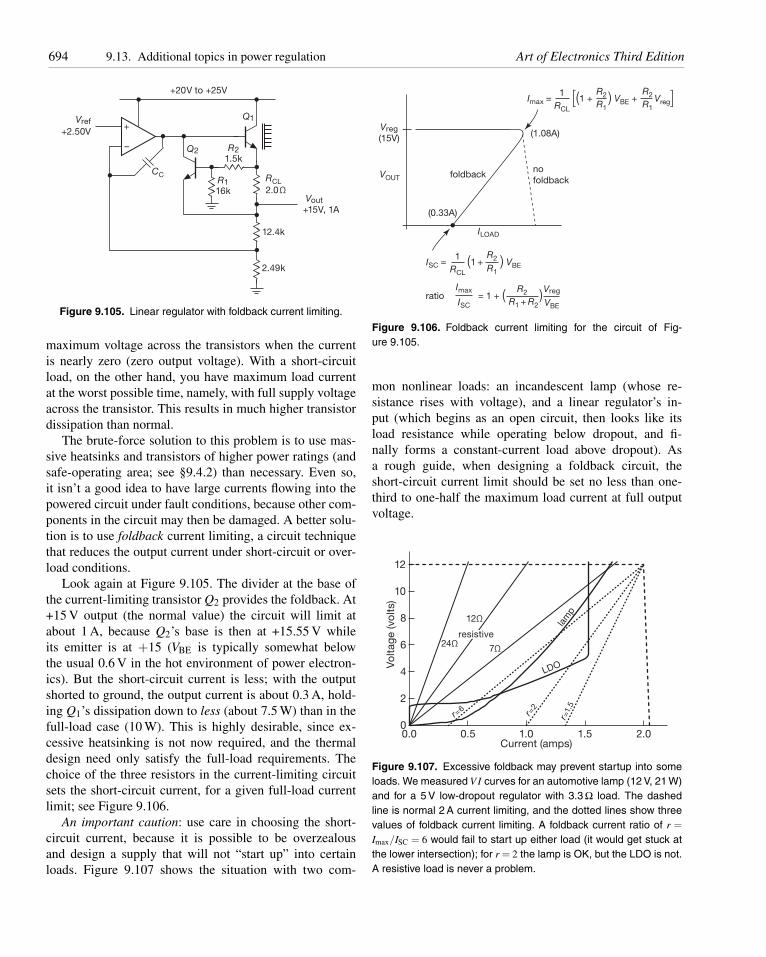
694 9.13. Additional topics in power regulation Art of Electronics Third Edition
+20V to +25V
Q1
Q2
CC
Vref
+2.50V
R2
1.5k
Vout
+15V, 1A
RCL
2.0ΩR1
16k
+
–
12.4k
2.49k
Figure 9.105. Linear regulator with foldback current limiting.
maximum voltage across the transistors when the currentis nearly zero (zero output voltage). With a short-circuitload, on the other hand, you have maximum load currentat the worst possible time, namely, with full supply voltageacross the transistor. This results in much higher transistordissipation than normal.
The brute-force solution to this problem is to use mas-sive heatsinks and transistors of higher power ratings (andsafe-operating area; see §9.4.2) than necessary. Even so,it isn’t a good idea to have large currents flowing into thepowered circuit under fault conditions, because other com-ponents in the circuit may then be damaged. A better solu-tion is to use foldback current limiting, a circuit techniquethat reduces the output current under short-circuit or over-load conditions.
Look again at Figure 9.105. The divider at the base ofthe current-limiting transistor Q2 provides the foldback. At+15 V output (the normal value) the circuit will limit atabout 1 A, because Q2’s base is then at +15.55 V whileits emitter is at +15 (VBE is typically somewhat belowthe usual 0.6 V in the hot environment of power electron-ics). But the short-circuit current is less; with the outputshorted to ground, the output current is about 0.3 A, hold-ing Q1’s dissipation down to less (about 7.5 W) than in thefull-load case (10 W). This is highly desirable, since ex-cessive heatsinking is not now required, and the thermaldesign need only satisfy the full-load requirements. Thechoice of the three resistors in the current-limiting circuitsets the short-circuit current, for a given full-load currentlimit; see Figure 9.106.
An important caution: use care in choosing the short-circuit current, because it is possible to be overzealousand design a supply that will not “start up” into certainloads. Figure 9.107 shows the situation with two com-
foldbackno
foldback
(1.08A)
(0.33A)
Vreg
(15V)
VOUT
ratio = 1 + ( )R2
R1 + R2
Vreg
VBE
Imax
ISC
= (1 + ) VBE
R2
R1
1
RCL
ISC
ILOAD
= [(1 + ) VBE + Vreg]R2
R1
1
RCL
Imax
R2
R1
Figure 9.106. Foldback current limiting for the circuit of Fig-ure 9.105.
mon nonlinear loads: an incandescent lamp (whose re-sistance rises with voltage), and a linear regulator’s in-put (which begins as an open circuit, then looks like itsload resistance while operating below dropout, and fi-nally forms a constant-current load above dropout). Asa rough guide, when designing a foldback circuit, theshort-circuit current limit should be set no less than one-third to one-half the maximum load current at full outputvoltage.
12
10
8
6
4
2
0
Vo
ltag
e (v
olts
)
2.01.51.00.50.0Current (amps)
resistive
lam
p
LDO
24Ω
12Ω
7Ω
r=1.
5
r=2
r=6
Figure 9.107. Excessive foldback may prevent startup into someloads. We measured V I curves for an automotive lamp (12 V, 21 W)and for a 5 V low-dropout regulator with 3.3 Ω load. The dashedline is normal 2 A current limiting, and the dotted lines show threevalues of foldback current limiting. A foldback current ratio of r =Imax/ISC = 6 would fail to start up either load (it would get stuck atthe lower intersection); for r = 2 the lamp is OK, but the LDO is not.A resistive load is never a problem.
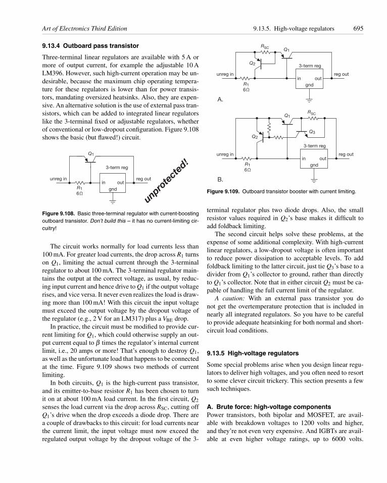
Art of Electronics Third Edition 9.13.5. High-voltage regulators 695
9.13.4 Outboard pass transistor
Three-terminal linear regulators are available with 5 A ormore of output current, for example the adjustable 10 ALM396. However, such high-current operation may be un-desirable, because the maximum chip operating tempera-ture for these regulators is lower than for power transis-tors, mandating oversized heatsinks. Also, they are expen-sive. An alternative solution is the use of external pass tran-sistors, which can be added to integrated linear regulatorslike the 3-terminal fixed or adjustable regulators, whetherof conventional or low-dropout configuration. Figure 9.108shows the basic (but flawed!) circuit.
reg out
R1
6Ω
unreg in
gnd
in out
3-term reg
Q1
unprote
cted
!
Figure 9.108. Basic three-terminal regulator with current-boostingoutboard transistor. Don’t build this – it has no current-limiting cir-cuitry!
The circuit works normally for load currents less than100 mA. For greater load currents, the drop across R1 turnson Q1, limiting the actual current through the 3-terminalregulator to about 100 mA. The 3-terminal regulator main-tains the output at the correct voltage, as usual, by reduc-ing input current and hence drive to Q1 if the output voltagerises, and vice versa. It never even realizes the load is draw-ing more than 100 mA! With this circuit the input voltagemust exceed the output voltage by the dropout voltage ofthe regulator (e.g., 2 V for an LM317) plus a VBE drop.
In practice, the circuit must be modified to provide cur-rent limiting for Q1, which could otherwise supply an out-put current equal to β times the regulator’s internal currentlimit, i.e., 20 amps or more! That’s enough to destroy Q1,as well as the unfortunate load that happens to be connectedat the time. Figure 9.109 shows two methods of currentlimiting.
In both circuits, Q1 is the high-current pass transistor,and its emitter-to-base resistor R1 has been chosen to turnit on at about 100 mA load current. In the first circuit, Q2
senses the load current via the drop across RSC, cutting offQ1’s drive when the drop exceeds a diode drop. There area couple of drawbacks to this circuit: for load currents nearthe current limit, the input voltage must now exceed theregulated output voltage by the dropout voltage of the 3-
reg out
R1
6Ω
unreg in
A.
gnd
in out
3-term reg
Q1
Q2
RSC
reg out
R1
6Ω
unreg in
B.
gnd
in out
3-term reg
Q1
Q2
Q3
RSC
Figure 9.109. Outboard transistor booster with current limiting.
terminal regulator plus two diode drops. Also, the smallresistor values required in Q2’s base makes it difficult toadd foldback limiting.
The second circuit helps solve these problems, at theexpense of some additional complexity. With high-currentlinear regulators, a low-dropout voltage is often importantto reduce power dissipation to acceptable levels. To addfoldback limiting to the latter circuit, just tie Q3’s base to adivider from Q1’s collector to ground, rather than directlyto Q1’s collector. Note that in either circuit Q2 must be ca-pable of handling the full current limit of the regulator.
A caution: With an external pass transistor you donot get the overtemperature protection that is included innearly all integrated regulators. So you have to be carefulto provide adequate heatsinking for both normal and short-circuit load conditions.
9.13.5 High-voltage regulators
Some special problems arise when you design linear regu-lators to deliver high voltages, and you often need to resortto some clever circuit trickery. This section presents a fewsuch techniques.
A. Brute force: high-voltage componentsPower transistors, both bipolar and MOSFET, are avail-able with breakdown voltages to 1200 volts and higher,and they’re not even very expensive. And IGBTs are avail-able at even higher voltage ratings, up to 6000 volts.
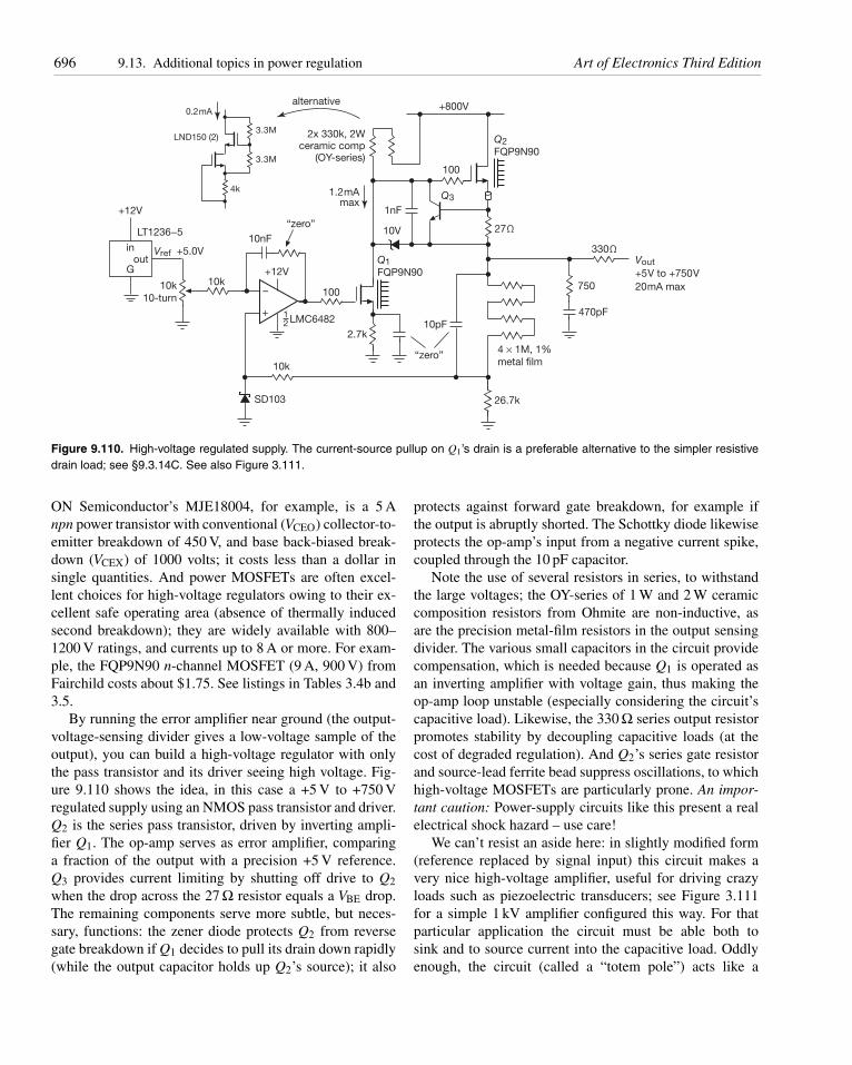
696 9.13. Additional topics in power regulation Art of Electronics Third Edition
+12V
+800Valternative
2x 330k, 2Wceramic comp
(OY-series)
10V
in
Gout
10k
10-turn
10k
330Ω
1.2mAmax
26.7k
4 × 1M, 1%
metal film
750
470pF
27Ω
10k
10pF2.7k
10nF
1nF
100
SD103
“zero”
“zero”
Vref +5.0VQ1
FQP9N90
LT1236−5
+
–
LMC648212
+12V
Q3
Q2
FQP9N90
Vout
+5V to +750V
20mA max
0.2mA
100
3.3M
3.3M
4k
LND150 (2)
Figure 9.110. High-voltage regulated supply. The current-source pullup on Q1’s drain is a preferable alternative to the simpler resistivedrain load; see §9.3.14C. See also Figure 3.111.
ON Semiconductor’s MJE18004, for example, is a 5 Anpn power transistor with conventional (VCEO) collector-to-emitter breakdown of 450 V, and base back-biased break-down (VCEX) of 1000 volts; it costs less than a dollar insingle quantities. And power MOSFETs are often excel-lent choices for high-voltage regulators owing to their ex-cellent safe operating area (absence of thermally inducedsecond breakdown); they are widely available with 800–1200 V ratings, and currents up to 8 A or more. For exam-ple, the FQP9N90 n-channel MOSFET (9 A, 900 V) fromFairchild costs about $1.75. See listings in Tables 3.4b and3.5.
By running the error amplifier near ground (the output-voltage-sensing divider gives a low-voltage sample of theoutput), you can build a high-voltage regulator with onlythe pass transistor and its driver seeing high voltage. Fig-ure 9.110 shows the idea, in this case a +5 V to +750 Vregulated supply using an NMOS pass transistor and driver.Q2 is the series pass transistor, driven by inverting ampli-fier Q1. The op-amp serves as error amplifier, comparinga fraction of the output with a precision +5 V reference.Q3 provides current limiting by shutting off drive to Q2
when the drop across the 27 Ω resistor equals a VBE drop.The remaining components serve more subtle, but neces-sary, functions: the zener diode protects Q2 from reversegate breakdown if Q1 decides to pull its drain down rapidly(while the output capacitor holds up Q2’s source); it also
protects against forward gate breakdown, for example ifthe output is abruptly shorted. The Schottky diode likewiseprotects the op-amp’s input from a negative current spike,coupled through the 10 pF capacitor.
Note the use of several resistors in series, to withstandthe large voltages; the OY-series of 1 W and 2 W ceramiccomposition resistors from Ohmite are non-inductive, asare the precision metal-film resistors in the output sensingdivider. The various small capacitors in the circuit providecompensation, which is needed because Q1 is operated asan inverting amplifier with voltage gain, thus making theop-amp loop unstable (especially considering the circuit’scapacitive load). Likewise, the 330 Ω series output resistorpromotes stability by decoupling capacitive loads (at thecost of degraded regulation). And Q2’s series gate resistorand source-lead ferrite bead suppress oscillations, to whichhigh-voltage MOSFETs are particularly prone. An impor-tant caution: Power-supply circuits like this present a realelectrical shock hazard – use care!
We can’t resist an aside here: in slightly modified form(reference replaced by signal input) this circuit makes avery nice high-voltage amplifier, useful for driving crazyloads such as piezoelectric transducers; see Figure 3.111for a simple 1 kV amplifier configured this way. For thatparticular application the circuit must be able both tosink and to source current into the capacitive load. Oddlyenough, the circuit (called a “totem pole”) acts like a
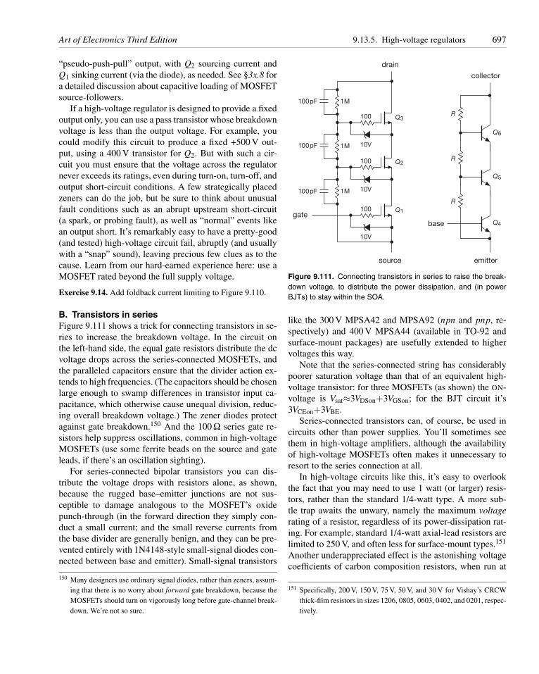
Art of Electronics Third Edition 9.13.5. High-voltage regulators 697
“pseudo-push-pull” output, with Q2 sourcing current andQ1 sinking current (via the diode), as needed. See §3x.8 fora detailed discussion about capacitive loading of MOSFETsource-followers.
If a high-voltage regulator is designed to provide a fixedoutput only, you can use a pass transistor whose breakdownvoltage is less than the output voltage. For example, youcould modify this circuit to produce a fixed +500 V out-put, using a 400 V transistor for Q2. But with such a cir-cuit you must ensure that the voltage across the regulatornever exceeds its ratings, even during turn-on, turn-off, andoutput short-circuit conditions. A few strategically placedzeners can do the job, but be sure to think about unusualfault conditions such as an abrupt upstream short-circuit(a spark, or probing fault), as well as “normal” events likean output short. It’s remarkably easy to have a pretty-good(and tested) high-voltage circuit fail, abruptly (and usuallywith a “snap” sound), leaving precious few clues as to thecause. Learn from our hard-earned experience here: use aMOSFET rated beyond the full supply voltage.
Exercise 9.14. Add foldback current limiting to Figure 9.110.
B. Transistors in seriesFigure 9.111 shows a trick for connecting transistors in se-ries to increase the breakdown voltage. In the circuit onthe left-hand side, the equal gate resistors distribute the dcvoltage drops across the series-connected MOSFETs, andthe paralleled capacitors ensure that the divider action ex-tends to high frequencies. (The capacitors should be chosenlarge enough to swamp differences in transistor input ca-pacitance, which otherwise cause unequal division, reduc-ing overall breakdown voltage.) The zener diodes protectagainst gate breakdown.150 And the 100 Ω series gate re-sistors help suppress oscillations, common in high-voltageMOSFETs (use some ferrite beads on the source and gateleads, if there’s an oscillation sighting).
For series-connected bipolar transistors you can dis-tribute the voltage drops with resistors alone, as shown,because the rugged base–emitter junctions are not sus-ceptible to damage analogous to the MOSFET’s oxidepunch-through (in the forward direction they simply con-duct a small current; and the small reverse currents fromthe base divider are generally benign, and they can be pre-vented entirely with 1N4148-style small-signal diodes con-nected between base and emitter). Small-signal transistors
150 Many designers use ordinary signal diodes, rather than zeners, assum-ing that there is no worry about forward gate breakdown, because theMOSFETs should turn on vigorously long before gate-channel break-down. We’re not so sure.
drain
collector
emitter
R
R
R
source
gate
1M
100
10V
10V
10V
Q3
Q6
100pF
100pF
100pF
1M
100 Q2
1M
100 Q1
Q5
base Q4
Figure 9.111. Connecting transistors in series to raise the break-down voltage, to distribute the power dissipation, and (in powerBJTs) to stay within the SOA.
like the 300 V MPSA42 and MPSA92 (npn and pnp, re-spectively) and 400 V MPSA44 (available in TO-92 andsurface-mount packages) are usefully extended to highervoltages this way.
Note that the series-connected string has considerablypoorer saturation voltage than that of an equivalent high-voltage transistor: for three MOSFETs (as shown) the ON-voltage is Vsat≈3VDSon+3VGSon; for the BJT circuit it’s3VCEon+3VBE.
Series-connected transistors can, of course, be used incircuits other than power supplies. You’ll sometimes seethem in high-voltage amplifiers, although the availabilityof high-voltage MOSFETs often makes it unnecessary toresort to the series connection at all.
In high-voltage circuits like this, it’s easy to overlookthe fact that you may need to use 1 watt (or larger) resis-tors, rather than the standard 1/4-watt type. A more sub-tle trap awaits the unwary, namely the maximum voltagerating of a resistor, regardless of its power-dissipation rat-ing. For example, standard 1/4-watt axial-lead resistors arelimited to 250 V, and often less for surface-mount types.151
Another underappreciated effect is the astonishing voltagecoefficients of carbon composition resistors, when run at
151 Specifically, 200 V, 150 V, 75 V, 50 V, and 30 V for Vishay’s CRCWthick-film resistors in sizes 1206, 0805, 0603, 0402, and 0201, respec-tively.
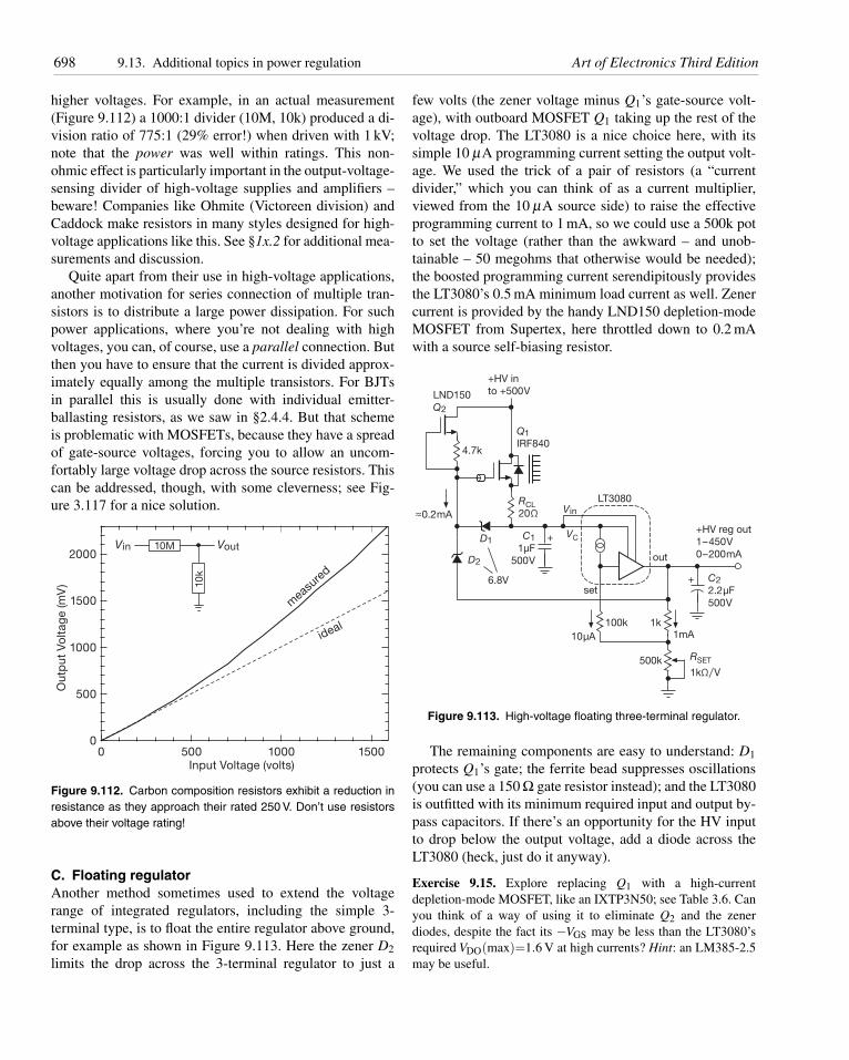
698 9.13. Additional topics in power regulation Art of Electronics Third Edition
higher voltages. For example, in an actual measurement(Figure 9.112) a 1000:1 divider (10M, 10k) produced a di-vision ratio of 775:1 (29% error!) when driven with 1 kV;note that the power was well within ratings. This non-ohmic effect is particularly important in the output-voltage-sensing divider of high-voltage supplies and amplifiers –beware! Companies like Ohmite (Victoreen division) andCaddock make resistors in many styles designed for high-voltage applications like this. See §1x.2 for additional mea-surements and discussion.
Quite apart from their use in high-voltage applications,another motivation for series connection of multiple tran-sistors is to distribute a large power dissipation. For suchpower applications, where you’re not dealing with highvoltages, you can, of course, use a parallel connection. Butthen you have to ensure that the current is divided approx-imately equally among the multiple transistors. For BJTsin parallel this is usually done with individual emitter-ballasting resistors, as we saw in §2.4.4. But that schemeis problematic with MOSFETs, because they have a spreadof gate-source voltages, forcing you to allow an uncom-fortably large voltage drop across the source resistors. Thiscan be addressed, though, with some cleverness; see Fig-ure 3.117 for a nice solution.
2000
1500
1000
500
0
Ou
tpu
t V
olt
ag
e (m
V)
150010005000Input Voltage (volts)
mea
sure
d
ideal
10M
10
k
Vin Vout
Figure 9.112. Carbon composition resistors exhibit a reduction inresistance as they approach their rated 250 V. Don’t use resistorsabove their voltage rating!
C. Floating regulatorAnother method sometimes used to extend the voltagerange of integrated regulators, including the simple 3-terminal type, is to float the entire regulator above ground,for example as shown in Figure 9.113. Here the zener D2
limits the drop across the 3-terminal regulator to just a
few volts (the zener voltage minus Q1’s gate-source volt-age), with outboard MOSFET Q1 taking up the rest of thevoltage drop. The LT3080 is a nice choice here, with itssimple 10 μA programming current setting the output volt-age. We used the trick of a pair of resistors (a “currentdivider,” which you can think of as a current multiplier,viewed from the 10 μA source side) to raise the effectiveprogramming current to 1 mA, so we could use a 500k potto set the voltage (rather than the awkward – and unob-tainable – 50 megohms that otherwise would be needed);the boosted programming current serendipitously providesthe LT3080’s 0.5 mA minimum load current as well. Zenercurrent is provided by the handy LND150 depletion-modeMOSFET from Supertex, here throttled down to 0.2 mAwith a source self-biasing resistor.
≈0.2mA
1mA
+HV reg out
1–450V
0–200mA
6.8V
4.7k
+HV in
to +500VLND150
Q2
Q1
IRF840
LT3080
out
set
100k 1k
500k
+
+
Vin
D1
RSET
1kΩ/V
VCC1
1μF
500V
C2
2.2μF
500V
D2
RCL
20Ω
10μA
Figure 9.113. High-voltage floating three-terminal regulator.
The remaining components are easy to understand: D1
protects Q1’s gate; the ferrite bead suppresses oscillations(you can use a 150 Ω gate resistor instead); and the LT3080is outfitted with its minimum required input and output by-pass capacitors. If there’s an opportunity for the HV inputto drop below the output voltage, add a diode across theLT3080 (heck, just do it anyway).
Exercise 9.15. Explore replacing Q1 with a high-currentdepletion-mode MOSFET, like an IXTP3N50; see Table 3.6. Canyou think of a way of using it to eliminate Q2 and the zenerdiodes, despite the fact its −VGS may be less than the LT3080’srequired VDO(max)=1.6 V at high currents? Hint: an LM385-2.5may be useful.
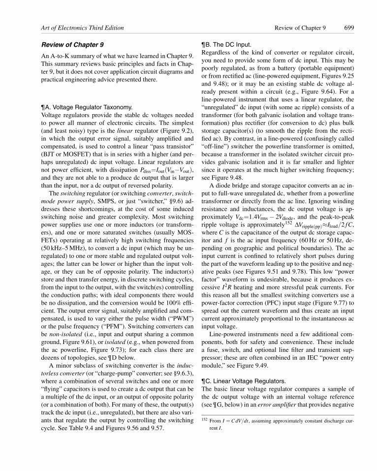
Art of Electronics Third Edition Review of Chapter 9 699
Review of Chapter 9
An A-to-K summary of what we have learned in Chapter 9.This summary reviews basic principles and facts in Chap-ter 9, but it does not cover application circuit diagrams andpractical engineering advice presented there.
¶A. Voltage Regulator Taxonomy.Voltage regulators provide the stable dc voltages neededto power all manner of electronic circuits. The simplest(and least noisy) type is the linear regulator (Figure 9.2),in which the output error signal, suitably amplified andcompensated, is used to control a linear “pass transistor”(BJT or MOSFET) that is in series with a higher (and per-haps unregulated) dc input voltage. Linear regulators arenot power efficient, with dissipation Pdiss=Iout(Vin−Vout),and they are not able to a produce dc output that is largerthan the input, nor a dc output of reversed polarity.
The switching regulator (or switching converter, switch-mode power supply, SMPS, or just “switcher,” §9.6) ad-dresses these shortcomings, at the cost of some inducedswitching noise and greater complexity. Most switchingpower supplies use one or more inductors (or transform-ers), and one or more saturated switches (usually MOS-FETs) operating at relatively high switching frequencies(50 kHz–5 MHz), to convert a dc input (which may be un-regulated) to one or more stable and regulated output volt-ages; the latter can be lower or higher than the input volt-age, or they can be of opposite polarity. The inductor(s)store and then transfer energy, in discrete switching cycles,from the input to the output, with the switch(es) controllingthe conduction paths; with ideal components there wouldbe no dissipation, and the conversion would be 100% effi-cient. The output error signal, suitably amplified and com-pensated, is used to vary either the pulse width (“PWM”)or the pulse frequency (“PFM”). Switching converters canbe non-isolated (i.e., input and output sharing a commonground, Figure 9.61), or isolated (e.g., when powered fromthe ac powerline, Figure 9.73); for each class there aredozens of topologies, see ¶D below.
A minor subclass of switching converter is the induc-torless converter (or “charge-pump” converter; see §9.6.3),where a combination of several switches and one or more“flying” capacitors is used to create a dc output that can bea multiple of the dc input, or an output of opposite polarity(or a combination of both). For many of these, the output(s)track the dc input (i.e., unregulated), but there are also vari-ants that regulate the output by controlling the switchingcycle. See Table 9.4 and Figures 9.56 and 9.57.
¶B. The DC Input.Regardless of the kind of converter or regulator circuit,you need to provide some form of dc input. This may bepoorly regulated, as from a battery (portable equipment)or from rectified ac (line-powered equipment, Figures 9.25and 9.48); or it may be an existing stable dc voltage al-ready present within a circuit (e.g., Figure 9.64). For aline-powered instrument that uses a linear regulator, the“unregulated” dc input (with some ac ripple) consists of atransformer (for both galvanic isolation and voltage trans-formation) plus rectifier (for conversion to dc) plus bulkstorage capacitor(s) (to smooth the ripple from the recti-fied ac). By contrast, in a line-powered (confusingly called“off-line”) switcher the powerline transformer is omitted,because a transformer in the isolated switcher circuit pro-vides galvanic isolation and it is far smaller and lightersince it operates at the much higher switching frequency;see Figure 9.48.
A diode bridge and storage capacitor converts an ac in-put to full-wave unregulated dc, whether from a powerlinetransformer or directly from the ac line. Ignoring windingresistance and inductances, the dc output voltage is ap-proximately Vdc=1.4Vrms − 2Vdiode, and the peak-to-peakripple voltage is approximately152 ΔVripple(pp)≈Iload/2 fC,where C is the capacitance of the output dc storage capac-itor and f is the ac input frequency (60 Hz or 50 Hz, de-pending on geographic and political boundaries). The acinput current is confined to relatively short pulses duringthe part of the waveform leading up to the positive and neg-ative peaks (see Figures 9.51 and 9.78). This low “powerfactor” waveform is undesirable, because it produces ex-cessive I2R heating and more stressful peak currents. Forthis reason all but the smallest switching converters use apower-factor correction (PFC) input stage (Figure 9.77) tospread out the current waveform and thus create an inputcurrent approximately proportional to the instantaneous acinput voltage.
Line-powered instruments need a few additional com-ponents, both for safety and convenience. These includea fuse, switch, and optional line filter and transient sup-pressor; these are often combined in an IEC “power entrymodule,” see Figure 9.49.
¶C. Linear Voltage Regulators.The basic linear voltage regulator compares a sample ofthe dc output voltage with an internal voltage reference(see ¶G, below) in an error amplifier that provides negative
152 From I = C dV/dt, assuming approximately constant discharge cur-rent I.
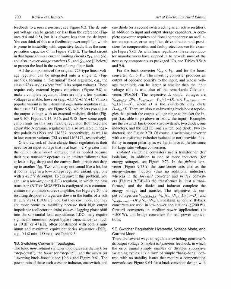
700 Review of Chapter 9 Art of Electronics Third Edition
feedback to a pass transistor; see Figure 9.2. The dc out-put voltage can be greater or less than the reference (Fig-ures 9.4 and 9.5), but it is always less than the dc input.You can think of this as a feedback power amplifier, whichis prone to instability with capacitive loads, thus the com-pensation capacitor Cc in Figure 9.2D,E. The final circuitin that figure shows a current limiting circuit (RCL and Q2),and also an overvoltage crowbar (D1 and Q3, see ¶J below)to protect the load in the event of a regulator fault.
All the components of the original 723-type linear volt-age regulator can be integrated onto a single IC (Fig-ure 9.6), forming a “3-terminal” fixed regulator, e.g., theclassic 78xx-style (where “xx” is its output voltage). Theserequire only external bypass capacitors (Figure 9.8) tomake a complete regulator. There are only a few standardvoltages available, however (e.g., +3.3 V, +5 V, +15 V); so apopular variant is the 3-terminal adjustable regulator (e.g.,the classic 317-type, see Figure 9.9), which lets you adjustthe output voltage with an external resistive divider (Fig-ure 9.10). Figures 9.14, 9.16, and 9.18 show some appli-cation hints for this very flexible regulator. Both fixed andadjustable 3-terminal regulators are also available in nega-tive polarities (79xx and LM337, respectively), as well asin low-current variants (78Lxx and LM317L, respectively).
One drawback of these classic linear regulators is theirneed for an input voltage that is at least ∼2 V greater thanthe output (its dropout voltage); that is needed becausetheir pass transistor operates as an emitter follower (thusat least a VBE drop) and the current-limit circuit can dropup to another VBE. Two volts may not sound like a lot, butit looms large in a low-voltage regulator circuit, e.g., onewith a +2.5 V dc output. To circumvent this problem, youcan use a low-dropout (LDO) regulator, in which the passtransistor (BJT or MOSFET) is configured as a common-emitter (or common-source) amplifier, see Figure 9.20; theresulting dropout voltages are down in the tenths of a volt(Figure 9.24). LDOs are nice, but they cost more, and theyare more prone to instability because their high outputimpedance (collector or drain) causes a lagging phase shiftinto the substantial load capacitance. LDOs may requiresignificant minimum output bypass capacitance (as muchas 10 μF or 47 μF), often constrained with both a min-imum and maximum equivalent series resistance (ESR),e.g., 0.1 Ω min, 1 Ω max; see Table 9.3.
¶D. Switching Converter Topologies.The basic non-isolated switcher topologies are the buck (or“step-down”), the boost (or “step-up”), and the invert (or“inverting buck–boost”); see §9.6.4 and Figure 9.61. Thepower train of these each uses one inductor, one switch, and
one diode (or a second switch acting as an active rectifier),in addition to input and output storage capacitors. A com-plete converter requires additional components: an oscilla-tor, comparator, error amplifier, drive circuits, and provi-sions for compensation and fault protection; see for exam-ple Figure 9.65. As with linear regulators, the semiconduc-tor manufacturers have stepped in to provide most of thenecessary components as packaged ICs, see Tables 9.5a,band 9.6.
For the buck converter Vout < Vin, and for the boostconverter Vout > Vin. The inverting converter produces anoutput of opposite polarity to the input, and whose volt-age magnitude can be larger or smaller than the inputvoltage (this is true also of the remarkable Cuk con-verter, §9.6.8H). The respective dc output voltages areVout(buck)=DVin, Vout(boost)=Vin/(1−D), and Vout(invert)=−VinD/(1−D), where D is the switch-ON duty cycleD=ton/T . There are also non-inverting buck-boost topolo-gies that permit the output voltage range to bracket the in-put (i.e., able to go above or below the input). Examplesare the 2-switch buck–boost (two switches, two diodes, oneinductor), and the SEPIC (one switch, one diode, two in-ductors), see Figure 9.70. Of course, a switching converterwith a transformer (whether isolated or not) provides flex-ibility in output polarity, as well as improved performancefor large ratio voltage conversion.
Isolated switching converters use a transformer (forisolation), in addition to one or more inductors (forenergy storage), see Figure 9.73. In the flyback con-verter (Figure 9.73A) the transformer acts also as theenergy-storage inductor (thus no additional inductor),whereas in the forward converter and bridge convert-ers (Figures 9.73B–D) the transformer is “just a trans-former,” and the diodes and inductor complete theenergy storage and transfer. The respective dc out-put voltages are Vout(flyback)=Vin[Nsec/Npri][D/(1−D)] andVout(forward)=DVin(Nsec/Npri). Speaking generally, flybackconverters are used in low-power applications (�200 W),forward converters in medium-power applications (to∼500 W), and bridge converters for real power applica-tions.
¶E. Switcher Regulation: Hysteretic, Voltage Mode, andCurrent Mode.There are several ways to regulate a switching converter’sdc output voltage. Simplest is hysteretic feedback, in whichthe error signal simply enables or disables successiveswitching cycles. It’s a form of simple “bang–bang” con-trol, with no stability issues that require a compensationnetwork; see Figure 9.64 for a buck converter design with
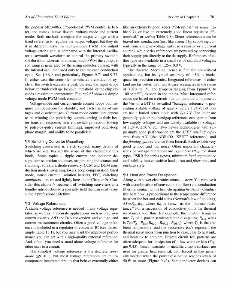
Art of Electronics Third Edition Review of Chapter 9 701
the popular MC34063. Proportional PWM control is bet-ter, and comes in two flavors: voltage mode and currentmode. Both methods compare the output voltage with afixed reference to regulate the output voltage, but they doit in different ways. In voltage-mode PWM, the outputvoltage error signal is compared with the internal oscilla-tor’s sawtooth waveform to control the primary switch’sON duration, whereas in current-mode PWM the compari-son ramp is generated by the rising inductor current, withthe internal oscillator used only to initiate each conductioncycle. See §9.6.9, and particularly Figures 9.71 and 9.72.In either case the controller terminates a conduction cy-cle if the switch exceeds a peak current, the input dropsbelow an “undervoltage lockout” threshold, or the chip ex-ceeds a maximum temperature. Figure 9.65 shows a simplevoltage-mode PWM buck converter.
Voltage-mode and current-mode control loops both re-quire compensation for stability, and each has its advan-tages and disadvantages. Current-mode controllers appearto be winning the popularity contest, owing to their bet-ter transient response, inherent switch protection (owingto pulse-by-pulse current limiting), improved outer-loopphase margin, and ability to be paralleled.
¶F. Switching Converter Miscellany.Switching conversion is a rich subject, many details ofwhich are well beyond the scope of this chapter (or thisbook). Some topics – ripple current and inductor de-sign, core saturation and reset, magnetizing inductance andsnubbing, soft start, diode recovery, CCM and DCM con-duction modes, switching losses, loop compensation, burstmode, inrush current, isolation barriers, PFC, switchingamplifiers – are treated lightly here and in Chapter 9x. Con-sider this chapter’s treatment of switching converters as alengthy introduction to a specialty field that can easily con-sume a professional lifetime.
¶G. Voltage References.A stable voltage reference is needed in any voltage regu-lator, as well as in accurate applications such as precisioncurrent sources, A/D and D/A conversion, and voltage- andcurrent-measurement circuits. Often a good voltage refer-ence is included in a regulator or converter IC (see for ex-ample Table 13.1), but you may want the improved perfor-mance you can get with a high-quality external reference.And, often, you need a stand-alone voltage reference forother uses in a circuit.
The simplest voltage reference is the discrete zenerdiode (§9.10.1), but most voltage references are multi-component integrated circuits that behave externally either
like an extremely good zener (“2-terminal,” or shunt; Ta-ble 9.7), or like an extremely good linear regulator (“3-terminal,” or series; Table 9.8). Shunt references must bebiased into conduction (just like a zener) by supplying cur-rent from a higher-voltage rail (use a resistor or a currentsource), while series references are powered by connectingtheir supply pin directly to the dc supply. References of ei-ther type are available in a small set of standard voltages,typically in the range of 1.25–10.0 V.
The discrete 2-terminal zener is fine for non-criticalapplications, but its typical accuracy of ±5% is inade-quate for precision circuits. Integrated references of eitherkind are far better, with worst-case accuracies in the rangeof 0.02% to 1%, and tempcos ranging from 1 ppm/◦C to100 ppm/◦C, as seen in the tables. Most integrated refer-ences are based on a circuit that temperature compensatesthe VBE of a BJT (a so-called “bandgap reference”), gen-erating a stable voltage of approximately 1.24 V; but oth-ers use a buried zener diode with VZ≈7 V. The latter aregenerally quieter, but bandgap references can operate fromlow supply voltages and are widely available in voltagesof 1.24 V, 2.50 V, etc. Two newer technologies with sur-prisingly good performance are the JFET pinchoff refer-ence from ADI (the ADR400 “XFET” references), andthe floating-gate reference from Intersil. Both exhibit verygood tempco and low noise. Other important character-istics of voltage references are regulation (Rout for shunttypes, PSRR for series types), minimum load capacitanceand stability into capacitive loads, trim and filter pins, andpackage style.
¶H. Heat and Power Dissipation.Along with power electronics comes. . . heat! You remove itwith a combination of convection (air flow) and conduction(thermal contact with a heat-dissipating heatsink). Conduc-tive heat flow is proportional to the temperature differencebetween the hot and cold sides (Newton’s law of cooling),ΔT=PdissRΘ, where RΘ is known as the “thermal resis-tance.” For a succession of conductive joints the thermalresistances add; thus, for example, the junction tempera-ture TJ of a power semiconductor dissipating Pdiss wattsis TJ=TA+Pdiss(RΘJC+RΘCS+RΘSA), where TA is the am-bient temperature, and the successive RΘ’s represent thethermal resistances from junction to case, case to heatsink,and heatsink to ambient. Printed circuit foil patterns areoften adequate for dissipation of a few watts or less (Fig-ure 9.45); finned heatsinks or metallic chassis surfaces areused for greater heat removal, with forced airflow gener-ally needed when the power dissipation reaches levels of50 W or more (Figure 9.43). Semiconductor devices can
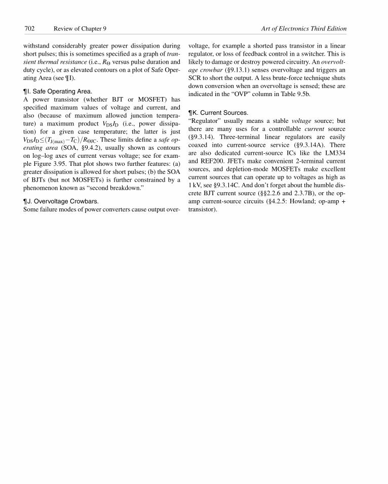
702 Review of Chapter 9 Art of Electronics Third Edition
withstand considerably greater power dissipation duringshort pulses; this is sometimes specified as a graph of tran-sient thermal resistance (i.e., RΘ versus pulse duration andduty cycle), or as elevated contours on a plot of Safe Oper-ating Area (see ¶I).
¶I. Safe Operating Area.A power transistor (whether BJT or MOSFET) hasspecified maximum values of voltage and current, andalso (because of maximum allowed junction tempera-ture) a maximum product VDSID (i.e., power dissipa-tion) for a given case temperature; the latter is justVDSID≤(TJ(max)−TC)/RΘJC. These limits define a safe op-erating area (SOA, §9.4.2), usually shown as contourson log–log axes of current versus voltage; see for exam-ple Figure 3.95. That plot shows two further features: (a)greater dissipation is allowed for short pulses; (b) the SOAof BJTs (but not MOSFETs) is further constrained by aphenomenon known as “second breakdown.”
¶J. Overvoltage Crowbars.Some failure modes of power converters cause output over-
voltage, for example a shorted pass transistor in a linearregulator, or loss of feedback control in a switcher. This islikely to damage or destroy powered circuitry. An overvolt-age crowbar (§9.13.1) senses overvoltage and triggers anSCR to short the output. A less brute-force technique shutsdown conversion when an overvoltage is sensed; these areindicated in the “OVP” column in Table 9.5b.
¶K. Current Sources.“Regulator” usually means a stable voltage source; butthere are many uses for a controllable current source(§9.3.14). Three-terminal linear regulators are easilycoaxed into current-source service (§9.3.14A). Thereare also dedicated current-source ICs like the LM334and REF200. JFETs make convenient 2-terminal currentsources, and depletion-mode MOSFETs make excellentcurrent sources that can operate up to voltages as high as1 kV, see §9.3.14C. And don’t forget about the humble dis-crete BJT current source (§§2.2.6 and 2.3.7B), or the op-amp current-source circuits (§4.2.5: Howland; op-amp +transistor).