Embed Size (px)
Citation preview
W e be l i eve the key to the 10 's longev i ty is its bas ica l ly s imple , c lean s t ruc ture wi th a d e q u a t e l y large (one M b y t e ) address space tha t a l lows users to get work done . In this way , it has evo lved eas i ly wi th use and with t echno logy . A n equa l ly s ignif icant fac tor in its success is a single o p e r a t i n g sys tem e n v i r o n m e n t enab l ing user p r o g r a m shar ing a m o n g all mach ines . The mach ine has thus a t t r a c t ed users who have bui l t s ignif icant l anguages and app l i ca t ions in a va r ie ty of env i ronmen t s . These u s e r - d e v e l o p e r s a re thus the d o m i n a n t sys tem a rch i t ec t s - imp lemen to r s .
In r e t ro spec t , the mach ine t u rned out to be l a rge r and fu r the r f rom a m i n i c o m p u t e r than we expec t ed . A s such it could easi ly have d ied o r d e s t r o y e d the t iny D E C organ iza t ion tha t s t a r t ed it. W e hope that this p a p e r has p rov ided insight in to the in te rac t ions of its d e v e l o p m e n t .
Acknowledgments . D a n S iewio rek dese rves ou r g rea tes t thanks for he lp ing with a c o m p l e t e ed i t ing of the text . The re fe rees and ed i to r s have been espec ia l ly helpful . The i m p o r t a n t p r o g r a m con t r ibu t ions by users a re too n u m e r o u s for us to give by name but he re a re most of them: APL, Basic , BLISS, DDT, LISP, Pasca l , S imula , sos , TECO, and Tenex . L ikewise , t he re have been so many con t r ibu t ions to the 10 's a rch i t ec tu re and i m p l e m e n t a t i o n s within D E C and t h r o u g h o u t the user c o m m u n i t y tha t we da re not give wha t wou ld be a pa r t i a l list.
Received April 1977; revised September 1977
References 1. Bell, G., Cady, R., McFarland, H., Delagi, B., O'Laughlin, J., and Noonan, R. A new architecture for minicomputers---,the DEC PDP-11. Proc. AFIPS 1970 SJCC, Vol. 36, AFIPS Press, Montvale, N.J., pp. 657-675. 2. Bell, G., and Freeman, P. C a i - A computer architecture for AI research AFIPS Conf. Proc. Vol. 38 (Spring, 1971), 779-790. 3. Bell, G., and Newell, A. Computer Structures: Readings and Examples. McGraw-Hill, New York, 1971. 4. Bobrow, D.G., Burchfiel, J.D., Murphy, D. L., and Tomlinson, R.S. TENEX, A Paged Time Sharing System for the PDP-10. Comm. ACM 15, 3 (March 1972), 135-143. 5. Bullman, D.M. Editor, stack computers issue. Computer 10, 5 (May 1977), 14-52. 6. Clark, W.A. The Lincoln TX-2 computer. Proc. WJCC 1957, Vol. 11, pp. 143-171. 7. Lunde, A. Empirical evaluation of some features of Instruction Set Processor architecture. Comm. ACM 20, 3 (March 1977), 143- 152. 8. Mitchell, J.L., and Olsen, K.H. TX-0, a transistor computer. Proc. EJCC 1956, Vol. 10, pp. 93-100. 9. McCarthy, J. Time Sharing Computer Systems, Management and the Computer of the Future M. Greenberger, Ed., M.I.T. Press, Cambridge, Mass., 1962, pp. 221-236. 10. Murphy, D.L. Storage organization and management in TENEX. Proc. AFIPS 1972 FJCC, Vol. 41, Pt. I, AFIPS Press, Montvale, N.J., pp. 23-32. 11. Olsen, K.H. Transistor circuitry in the Lincoln TX-2. Proc. WJCC 1957, Vol. 11, pp. 167-171. 12. Roberts, L.G. Ed. Section on Resource Sharing Computer Networks. AFIPS 1970 SJCC, Vol. 36, AFIPS Press, Montvale, N.J., pp. 543-598. 13. Wulf, W., and Bell, G. C.mmp--A mutli-mini-processor. Proc. AFIPS 1972 FJCC, Vol. 41, AFIPS Press, Montvale, N.J., pp. 765-777. 14. Wulf, W., Russell, D., and Habermann, A.N. BLISS: A language for systems programming. Comm. ACM 14, 12 (Dec. 1971), 780-790.
63
C o m p u t e r Sys tems
G . Bel l , S. H . Fu l l e r , and D. S i ewio rek , E d i t o r s
The CRAY- 1 Computer System R i c h a r d M . R u s s e l l C r a y R e s e a r c h , I n c .
This paper describes the C R A Y , 1 , discusses the evolution of its architecture, and gives an account of some of the problems that were overcome during its manufacture.
The CRAY-1 is the only computer to have been built to date that satisfies ERDA's Class VI requirement (a computer capable of processing from 20 to 60 million floating point operations per second) [11.
The CRAY-I 's Fortran compiler (CVT) is designed to give the scientific user immediate access to the benefits of the C R A Y - r s vector processing architecture. An optimizing compBer, cFr, "vectorizes" innermost D O loops. Compatible with the ANSI 1966 Fortran Standard and with many commonly supported Fortran extensions, CVT does not require any source program modifications or the use of additional nonstandard Fortran statements to achieve vectorization. Thus the user's investment of hundreds of man months of effort to develop Fortran programs for other contemporary computers is protected.
Key Words and Phrases: architecture, computer systems
CR Categories: 1.2, 6.2, 6.3
Introduction
V e c t o r p rocessors a re no t ye t c o m m o n p l a c e ma- chines in the la rger -sca le c o m p u t e r ma rke t . A t the t ime of this wri t ing we know of only 12 n o n - C R A Y - 1 vec to r p roces so r ins ta l la t ions wor ldwide . O f these 12, the mos t power fu l p roces so r is the I L L I A C I V (1 ins ta l l a t ion) , the mos t p o p u l o u s is the Texas Ins t ru- men t s A d v a n c e d Scientif ic C o m p u t e r (7 ins ta l la t ions) and the mos t pub l i c ized is Con t ro l D a t a ' s S T A R 100
Copyright © 1977, Association for Computing Machinery, Inc. General permission to republish, but not for profit, all or part of this material is granted provided that ACM's copyright notice is given and that" reference is made to the publication, to its date of issue, and to the fact that reprinting privileges were granted by permission of the Association for Computing Machinery.
Author's address: Cray Research Inc., Suite 213, 7850 Metro Parkway, Minneapolis, MN 55420.
Communications January 1978 of Volume 21 the ACM Number 1
(4 installations). In its report on the CRAY-1, Auer- bach Computer Technology Reports published a com- parison of the CRAY-1, the ASC, and the STAR 100 [2]. The CRAY-1 is shown to be a more powerful computer than any of its main competi tors and is est imated to be the equivalent of five IBM 370/195s.
Independent benchmark studies have shown the CRAY-1 fully capable of supporting computat ional rates of 138 million floating-point operations per sec- ond (MFLOPS) for sustained periods and even higher rates of 250 MrLOPS in short bursts [3, 4]. Such comparat ively high performance results from the CRAY-1 internal architecture, which is designed to accommodate the computat ional needs of carrying out many calculations in discrete steps, with each step producing interim results used in subsequent steps. Through a technique called "chaining," the CRAY-1 vector functional units, in combination with scalar and vector registers, generate interim results and use them again immediately without additional memory refer- ences, which slow down the computat ional process in other contemporary computer systems.
Other features enhancing the C R A Y - I ' s computa- tional capabilities are: its small size, which reduces distances electrical signals must travel within the com- puter 's f ramework and allows a 12.5 nanosecond clock period (the CRAY-1 is the world's fastest scalar proc- essor); a one million word semiconductor memory equipped with error detection and correction logic (SECD~D); its 64-bit word size; and its optimizing Fortran compiler.
Architecture
The CRAY-1 has been called " the world's most expensive love-seat" [5]. Certainly, most people 's first reaction to the C R A Y - I is that it is so small. But in computer design it is a truism that smaller means faster. The greater the separation of components , the longer the time taken for a signal to pass between them. A cylindrical shape was chosen for the CRAY-1 in order to keep wiring distances small.
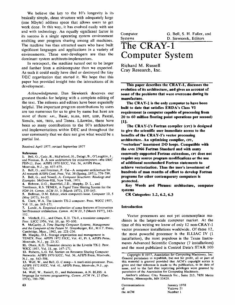
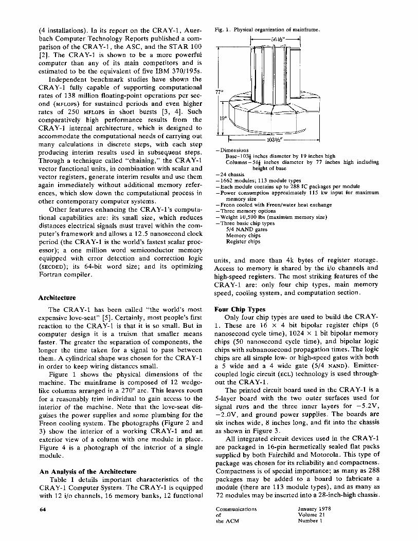
Figure 1 shows the physical dimensions of the machine. The mainframe is composed of 12 wedge- like columns arranged in a 270 ° arc. This leaves room for a reasonably trim individual to gain access to the interior of the machine. Note that the love-seat dis- guises the power supplies and some plumbing for the Freon cooling system. The photographs (Figure 2 and 3) show the interior of a working CRAY-1 and an exterior view of a column with one module in place. Figure 4 is a photograph of the interior of a single module.
An Analysis of the Architecture Table I details important characteristics of the
CRAY-1 Compute r System. The CRAY-1 is equipped with 12 i/o channels, 16 memory banks, 12 functional
64
Fig. 1. Physical organization of mainframe.
1, 1031/2" ,I
- Dimensions Base-103½ inches diameter by 19 inches high Columns-56½ inches diameter by 77 inches high including
height of base --24 chassis - 1662 modules; 113 module types --Each module contains up to 288 IC packages per module -Power consumption approximately 115 kw input for maximum
memory size --Freon cooled with Freon/water heat exchange -Three memory options -Weight 10,500 lbs (maximUm memory size) -Three basic chip types
5/4 NAND gates Memory chips Register chips
units, and more than 4k bytes of register storage. Access to memory is shared by the i/o channels and high-speed registers. The most striking features of the CRAY-1 are: only four chip types, main memory speed, cooling system, and computat ion section.
Four Chip Types Only four chip types are used to build the CRAY-
1. These are 16 × 4 bit bipolar register chips (6 nanosecond cycle t ime), 1024 × 1 bit bipolar memory chips (50 nanosecond cycle t ime), and bipolar logic chips with subnanosecond propagat ion times. The logic chips are all simple low- or high-speed gates with both a 5 wide and a 4 wide gate (5/4 NAND). Emit ter- coupled logic circuit (ECL) technology is used through- out the CRAY-1 .
The printed circuit board used in the CRAY-1 is a 5-layer board with the two outer surfaces used for signal runs and the three inner layers for - 5 . 2 V , - 2 . 0 V , and ground power supplies. The boards are six inches wide, 8 inches long, and fit into the chassis as shown in Figure 3.
All integrated circuit devices used in the CRAY-1 are packaged in 16-pin hermetically sealed flat packs supplied by both Fairchild and Motorola . This type of package was chosen for its reliability and compactness. Compactness is of special importance; as many as 288 packages may be added to a board to fabricate a module (there are 113 module types), and as many as 72 modules may be inserted into a 28-inch-high chassis.
Communications January 1978 of Volume 21 the ACM Number 1
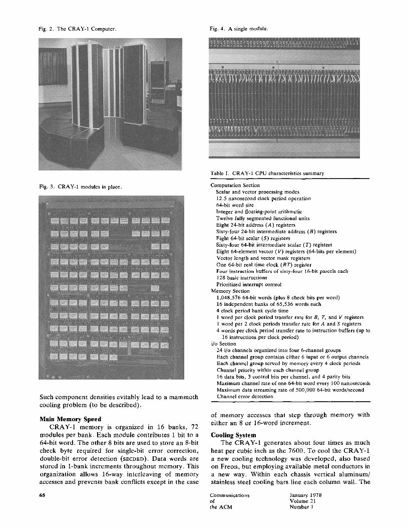
Fig. 2. The CRAY-1 Computer. Fig. 4. A single module.
Fig. 3. CRAY-1 modules in place.
Such component densities evitably lead to a mammoth cooling problem (to be described).
Main Memory Speed CRAY-1 memory is organized in 16 banks, 72
modules per bank. Each module contributes 1 bit to a 64-bit word. The other 8 bits are used to store an 8-bit check byte required for single-bit error correction, double-bit error detection (SECDEO). Data words are stored in 1-bank increments throughout memory. This organization allows 16-way interleaving of memory accesses and prevents bank conflicts except in the case
65
Table I. CRAY-1 CPU characteristics summary
Computation Section Scalar and vector processing modes 12.5 nanosecond clock period operation 64-bit word size Integer and floating-point arithmetic Twelve fully segmented functional units Eight 24-bit address (A) registers Sixty-four 24-bit intermediate address (B) registers Eight 64-bit scalar(S) registers Sixty-four 64-bit intermediate scalar (T) registers Eight 64-element vector (V) registers (64-bits per element) Vector length and vector mask registers One 64-bit real time clock (RT) register Four instruction buffers of sixty-four 16-bit parcels each 128 basic instructions Prioritized interrupt control
Memory Section 1,048,576 64-bit words (plus 8 check bits per word) 16 independent banks of 65,536 words each 4 clock period bank cycle time 1 word per clock period transfer rate for B, T, and V registers 1 word per 2 clock periods transfer rate for A and S registers 4 words per clock period transfer rate to instruction buffers (up to
16 instructions per clock period) i/o Section
24 i/o channels organized into four 6-channel groups Each channel group contains either 6 input or 6 output channels Each channel group served by memory every 4 clock periods Channel priority within each channel group 16 data bits, 3 control bits per channel, and 4 parity bits Maximum channel rate of one 64-bit word every 100 nanoseconds Maximum data streaming rate of 500,000 64-bit words/second Channel error detection
of memory accesses that step through memory with either an 8 or 16-word increment.
Cooling System The CRAY-1 generates about four times as much
heat per cubic inch as the 7600. To cool the CRAY-1 a new cooling technology was developed, also based on Freon, but employing available metal conductors in a new way. Within each chassis vertical aluminum/ stainless steel cooling bars line each column wall. The
Communications January 1978 of Volume 21 the ACM Number 1
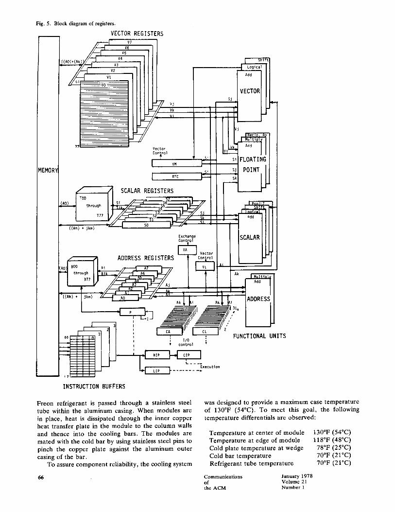
Fig. 5. Block diagram of registers.
VECTOR REGISTERS
4EMOR)
,K-'- '] v7 / ~ - i v6
//~-. I ' v5 ~ ~ _ . ~ v3 v4
Z.Z~ I vl v2 ....
/ j / co,' VO
Vector C o n t r o l
Vj Vk Vi
i .SJ I v. F
.~i
~ SCALAR REGISTERS oo
T77 s~ ~
((Ah) + jkm) ~'?" I SO ~--- -~-
~XCn~aonl ge
Vector ADDRESS REGISTERS
Shlftl
VECTOR I I
_F
vj
FLOATING
POINT
r
n | | ! J
l
I 71 I I I~
Ak
control
Ak
,,P
L,, F . . . .
INSTRUCTION BUFFERS
ADDRESS
FUNCTIONAL UNITS
Freon refrigerant is passed through a stainless steel tube within the aluminum casing. When modules are in place, heat is dissipated through the inner copper heat transfer plate in the module to the column walls and thence into the cooling bars. The modules are mated with the cold bar by using stainless steel pins to pinch the copper plate against the aluminum outer casing of the bar.
To assure component reliability, the cooling system
66
was designed to provide a maximum case temperature of 130°F (54°C). To meet this goal, the following temperature differentials are observed:
T e m p e r a t u r e at cen te r of m o d u l e T e m p e r a t u r e at edge of m o d u l e Cold p la te t e m p e r a t u r e at wedge Cold ba r t e m p e r a t u r e Re f r i ge r an t t ube t e m p e r a t u r e
130°F (54°C) l18°F (48°C)
78°F (25°C) 70°F (21°C) 70°F (21°C)
Communications January 1978 of Volume 21 the ACM Number 1
Functional Units There are 12 functional units, organized in four
groups: address, scalar, vector, and floating point. Each functional unit is pipelined into single clock segments. Functional unit t ime is shown in Table II . Note that all of the functional units can operate concur- rently so that in addition to the benefits of pipelining (each functional unit can be driven at a result rate of 1 per clock period) we also have parallelism across the units too. Note the absence of a divide unit in the CRAY-1. In order to have a completely segmented divide operat ion the CRAY-1 performs floating-point division by the method of reciprocal approximation. This technique has been used before (e.g. IBM System/ 360 Model 91).
Registers Figure 5 shows the CRAY-1 registers in relation-
ship to the functional units, instruction buffers, i/o channel control registers, and memory . The basic set of programmable registers are as follows:
8 24-bit address (A) registers 64 24-bit address-save (B) registers 8 64-bit scalar (S) registers 64 64-bit scalar-save (T) registers 8 64-word (4096-bit) vector (V) registers
Expressed in 8-bit bytes rather than 64-bit words, that 's a total of 4,888 bytes of high-speed (6ns) register storage.
The functional units take input operands from and store result operands only to A, S, and V registers. Thus the large amount of register storage is a crucial factor in the C R A Y - I ' s architecture. Chaining could not take place if vector register space were not availa- ble for the storage of final or intermediate results. The B and T registers greatly assist scalar performance. Temporary scalar values can be stored from and re- loaded to the A and S register in two clock periods. Figure 5 shows the C R A Y - I ' s register paths in detail. The speed of the eFT Fortran IV compiler would be seriously impaired if it were unable to keep the many Pass 1 and Pass 2 tables it needs in register space, Without the register storage provided by the B, T, and V registers, the C R A Y - I ' s bandwidth of only 80 million words/second would be a serious impediment to performance.
Instruction Formats Instructions are expressed in either one or two 16-
bit parcels. Below is the general form of a CRAY-1 instruction. Two-parcel instructions may overlap mem- ory-word boundaries, as follows: Fields g h i j k m
0-3 4-6 7-9 10-12 13 -15 16-31 Bit posi- (4) (3) (3) (3) (3) (16) tions
Parcel 1 Parcel 2
The computat ion section processes instructions at a maximum rate of one parcel per clock period.
Table II. CRAY-1 functional units
Functional Register unit time
usage (clock pe- riods)
Address function units address add unit A 2 address multiply unit A 6
Scalar functional units scalar add unit S scalar shift unit S
scalar logical unit S population/leading zero count
unit S 3 Vector functional units
vector add unit V 3 vector shift unit V 4 vector logical unit V 2
Floating-point functional units floating-point add unit S and V 6 floating-point multiply unit S and V 7 reciprocal approximation unit S and V 14
3 2 or 3 if double-
word shift 1
For arithmetic and logical instructions, a 7-bit op- eration code (gh) is followed by three 3-bit register designators. The first field, i, designates the result register. The j and k fields designate the two operand registers or are combined to designate a B or T register.
The shift and mask instructions consist of a 7-bit operat ion code (gh) followed by a 3-bit i field and a 6- bit jk field. The i field designates the operand register. The jk combined field specifies a shift or mask count.
Immedia te operand, read and store memory , and branch instructions require the two-parcel instruction word format. The immediate operand and the read and store memory instructions combine the j, k, and m fields to define a 22-bit quantity or memory address. In addition, the read and store memory instructions use the h field to specify an operating register for indexing. The branch instructions combine the i, j, k, and m fields into a 24-bit memory address field. This allows branching to any one of the four parcel positions in any 64-bit word, whether in memory or in an instruction buffer.
Operating Registers Five types of r e g i s t e r s - t h r e e primary (A, S, and
V) and two intermediate (B and T ) - a r e provided in the CRAY-1 .
A registers-eight 24-bit A registers serve a variety of applications. They are primarily used as address registers for memory references and as index registers, but also are used to provide values for shift counts, loop control, and channel i/o operations. In address applications, they are used to index the base address for scalar memory references and for providing both a base address and an index address for vector memory references.
The 24-bit integer functional units modify values
67 Communications January 1978 of Volume 21 the ACM Number 1
(such as program addresses) by adding, subtracting, and multiplying A register quantities. The results of these operations are returned to A registers.
Data can be transferred directly from memory to A registers or can be placed in B registers as an interme- diate step. This allows buffering of the data between A registers and memory. Data can also be transferred between A and S registers and from an A register to the vector length registers. The eight A registers are individually designated by the symbols A0, A1, A2, A3, A4, A5, A6, and A7.
B registers--there are sixty-four 24-bit B registers, which are used as auxiliary storage for the A registers. The transfer of an operand between an A and a B register requires only one clock period. Typically, B registers contain addresses and counters that are refer- enced over a longer period than would permit their being retained in A registers. A block of data in B registers may be transferred to or from memory at the rate of one clock period per register. Thus, it is feasible to store the contents of these registers in memory prior to calling a subroutine requiring their use. The sixty-four B registers are individually designated by the symbols B0, B1, B2 . . . . . and B778.
S registers -eight 64-bit S registers are the principle data handling registers for scalar operations. The S registers serve as both source and destination registers for scalar arithmetic and logical instructions. Scalar quantities involved in vector operations are held in S registers. Logical, shift, fixed-point, and floating-point operations may be performed on S register data. The eight S registers are individually designated by the symbols SO, S1, $2, $3, $4, $5, $6, and $7.
T registers -sixty-four 64-bit T registers are used as auxiliary storage for the S registers. The transfer of an operand between S and T registers requires one clock period. Typically, T registers contain operands that are referenced over a longer period than would permit their being retained in S registers. T registers allow intermediate results of complex computations to be held in intermediate access storage rather than in memory. A block of data in T registers may be transferred to or from memory at the rate of one word per clock period. The sixty-four T registers are individ- ually designated by the symbols TO, T1, T2 . . . . . and T778.
V registers-eight 64-element V registers provide operands to and receive results from the functional units at a one clock period rate. Each element of a V register holds a 64-bit quantity. When associated data is grouped into successive elements of a V register, the register may be considered to contain a vector. Exam- ples of vector quantities are rows and columns of a matrix, or similarly related elements of a table. Com- putational efficiency is achieved by processing each element of the vector identically. Vector merge and test instructions are provided in the CRAY-1 to allow operations to be performed on individual elements designated by the content of the vector mask (VM)
68
register. The number of vector register elements to be processed is contained in the vector length (VL) regis- ter. The eight V registers are individually designated by the symbols V0, V1, V2, V3, V4, V5, B6, and V7.
Supporting Registers The CPU contains a variety of additional registers
that support the control of program execution. These are the vector length (VL) and vector mask (VM) registers, the program counter (P), the base address (BA) and limit address (LA) registers, the exchange address (XA) register, the flag (F) register, and the mode (M) register.
VL register-the 64-bit vector mask (VM) register controls vector element designation in vector merge and test instructions. Each bit of the VM register corresponds to a vector register element. In the vector test instruction, the VM register content is defined by testing each element of a V register for a specific condition.
P register-the 24-bit P register specifies the mem- ory register parcel address of the current program instruction. The high order 22 bits specify a memory address and the low order two bits indicate a parcel number. This parcel address is advanced by one as each instruction parcel in a nonbranching sequence is executed and is replaced whenever program branching occurs.
BA registers- the 18-bit base address (BA) register contains the upper 18 bits of a 22-bit memory address. The lower four bits of this address are considered zeros. Just prior to initial or continued execution of a program, a process known as the "exchange sequence" stores into the BA register the upper 18 bits of the lowest memory address to be referenced during pro- gram execution. As the program executes, the address portion of each instruction referencing memory has its content added to that of the BA register. The sum then serves as the absolute address used for the mem- ory reference and ensures that memory addresses lower than the contents of the BA register are not accessed. Programs must, therefore, have all instructions refer- encing memory do so with their address portions containing relative addresses. This process supports program loading and memory protection operations and does not, in producing an absolute address, affect the content of the instruction buffer, BA, or memory.
LA register--the 18-bit limit address (LA) register contains the upper 18 bits of a 22-bit memory address. The lower 4 bits of this address are considered zeros. Just prior to initial or continued execution of a pro- gram, the "exchange sequence" process stores into the LA register the upper 18 bits of that absolute address one greater than allowed to be referenced by the program. When program execution begins, each in- struction referencing a memory location has the abso- lute address for that reference (determined by summing its address portion with the BA register contents) checked against the LA register content. If the absolute
Communications January 1978 of Volume 21 the ACM Number 1
address equals or exceeds the LA register content, an out-of-range error condition is flagged and program execution terminates. This process supports the mem- ory protection operat ion.
X A register ~ the 8-bit exchange address (XA) reg- ister contains the upper eight bits of a 12-bit memory address. The lower four bits of the address are consid- ered zeros. Because only twelve bits are used, with the lower four bits always being zeros, exchange addresses can reference only every 16th memory address begin- ning with address 0000 and concluding with address 4080. Each of these addresses designates the first word of a 16-word set. Thus, 256 sets (of 16 memory words each) can be specified. Prior to initiation or continuation of a program's execution, the XA register contains the first memory address of a particular 16- word set or exchange package. The exchange package contains certain operating and support registers ' con- tents as required for operations following an interrupt. The XA register supports the exchange sequence op- eration and the contents of XA are stored in an exchange package whenever an exchange sequence occurs.
F register-the 9-bit F register contains flags that, whenever set, indicate interrupt conditions causing initiation of an exchange sequence. The interrupt con- ditions are: normal exit, error exit, i/o interrupt, uncor- rected memory error, program range error, operand range error , floating-point overflow, real-t ime clock interrupt, and console interrupt.
M register-the M (mode) register is a three-bit register that contains part of the exchange package for a currently active program. The three bits are selec- tively set during an exchange sequence. Bit 37, the floating-point error mode flag, can be set or cleared during the execution interval for a program through use of the 0021 and 0022 instructions. The other two bits (bits 38 and 39) are not altered during the execu- tion interval for the exchange package and can only be altered when the exchange package is inactive in stor- age. Bits are assigned as follows in word two of the exchange package.
Bit 37 -F loa t i ng -po in t error mode flag. When this bit is set, interrupts on floating-point errors are enabled.
Bit 3 8 - U n c o r r e c t a b l e memory error mode flag. When this bit is set, interrupts on uncorrectable memory parity errors are enabled.
Bit 3 9 - M o n i t o r mode flag. When this bit is set, all interrupts other than parity errors are inhibited.
Integer Arithmetic All integer arithmetic is performed in 24-bit or 64-
bit 2's complement form.
Floating-Point Arithmetic Floating-point numbers are represented in signed
magnitude form. The format is a packed signed binary
69
fraction and a biased binary integer exponent . The fraction is a 49-bit signed magnitude value. The expo- nent is 15-bit biased. The unbiased exponent range is:
2 -2°°°°s to 2 +177778,
or approximately
10 -25o0 to 10 +25o0
An exponent equal to or greater than 2 +2°°°°8 is recog- nized by the floating-point functional units as an over- flow condition, and causes an interrupt if floating point interrupts are enabled.
Chaining The chaining technique takes advantage of the
parallel operation of functional units. Parallel vector operations may be processed in two ways: (a) using different functional units and V registers, and (b) chaining; that is, using the result s tream to one vector register simultaneously as the operand set for another operat ion in a different functional unit.
Parallel operations on vectors allow the generation of two or more results per clock period. A vector operat ion either uses two vector registers as sources of operands or uses one scalar register and one vector register as sources of operands. Vectors exceeding 64 elements are processed in 64-element segments.
Basically, chaining is a phenomenon that occurs when results issuing from one functional unit (at a rate of one/clock period) are immediately fed into another functional unit and so on. In other words, intermediate results do not have to be stored to memory and can be used even before the vector operation that created them runs to completion.
Chaining has been compared to the technique of "data forwarding" used in the IBM 360/195. Like data forwarding, chaining takes place automatically. Data forwarding consists of hardware facilities within the 195 floating-point processor communicating auto- matically by transferring "name tags," or internal codes between themselves [6]. Unlike the CRAY-1 , the user has no access to the 195's data-forwarding buffers. And, of course, the 195 can only forward scalar values, not entire vectors.
Interrupts and Exchange Sequence Interrupts are handled cleanly by the CRAY-1
hardware. Instruction issue is terminated by the hard- ware upon detection of an interrupt condition. All memory bank activity is allowed to complete as are any vector instructions that are in execution, and then an exchange sequence is activated. The Cray Operating System (cos) is always one partner of any exchange sequence. The cause of an interrupt is analyzed during an exchange sequence and all interrupts are processed until none remain.
Only the address and scalar registers are maintained in a program's exchange package (Fig. 6). The user 's B, T, and V registers are saved by the operating system in the user 's Job Table Area.
Communications January 1978 of Volume 21 the ACM Number 1
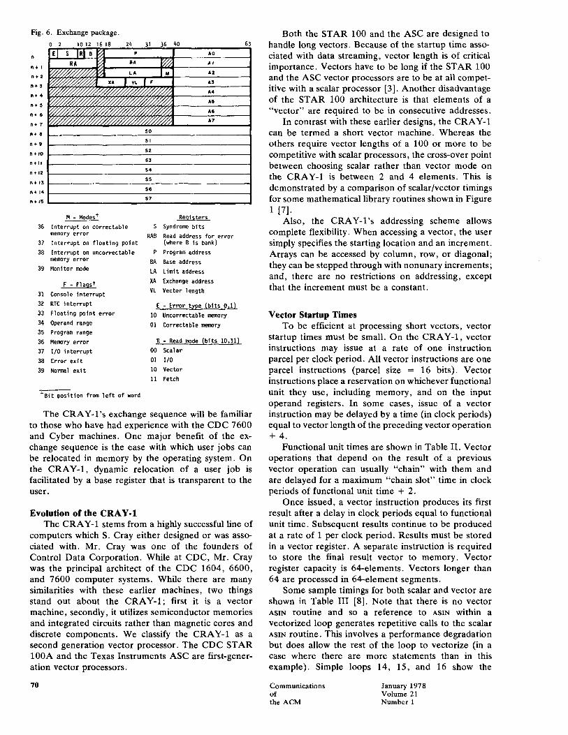
Fig. 6. Exchange package.
0 2 10 12 16 18 2h 31 36 ~0
n El s IH.L , ' n,, eA ~ ~ 8A ° . , LA l . . + , - I v < l ,
. . .
. . ,
n. " / / / / / / / / / / / / / / / / / / / / / / / / / / / / / / / / / / /Px n . ,
SO n + e
h e 9
n + l o
n~,l l
n+12
I1÷ 13
n~14
n+15
63 AO
A I
A2
a$
A4
A5
Aa
A?
S I
$2
S3
S4
S5
S6
S?
M - Modes + Registers
36 Interrupt on correctable S Syndrome bits
memory error RAB Read address for error 37 Interrupt on floating point (where B is bank)
38 Interrupt on uncorrectable P Program address memory error BA Base address
39 Monitor mode LA Limit address
F - Flags + XA Exchange address VL Vector length 31 Console interrupt
32 RTC interrupt E - Error type (bits 0,1)
33 Floating point error 10 Uncorrectable memory
34 Operand range Ol Correctable memory 35 Program range 36 Memory error R - Read mode (bits 10,11)
37 I/O interrupt O0 Scalar
38 Error exit 01 I/O
39 Normal exi t I0 Vector
11 Fetch
i B i t position from l e f t of word
The C R A Y - I ' s exchange sequence will be familiar to those who have had experience with the CDC 7600 and Cyber machines. One major benefit of the ex- change sequence is the ease with which user jobs can be relocated in memory by the operating system. On the CRAY-1 , dynamic relocation of a user job is facilitated by a base register that is t ransparent to the user.
Evolution o f the C R A Y - 1 The CRAY-1 stems f rom a highly successful line of
computers which S. Cray either designed or was asso- ciated with. Mr. Cray was one of the founders of Control Data Corporat ion. While at CDC, Mr. Cray was the principal architect of the CDC 1604, 6600, and 7600 computer systems. While there are many similarities with these earlier machines, two things stand out about the CRAY-1 ; first it is a vector machine, secondly, it utilizes semiconductor memories and integrated circuits rather than magnetic cores and discrete components . We classify the CRAY-1 as a second generation vector processor. The CDC STAR 100A and the Texas Instruments ASC are first-gener- ation vector processors.
70
Both the STAR 100 and the ASC are designed to handle long vectors. Because of the startup time asso- ciated with data streaming, vector length is of critical importance. Vectors have to be long if the STAR 100 and the ASC vector processors are to be at all compet- itive with a scalar processor [3]. Another disadvantage of the STAR 100 architecture is that elements of a "vec tor" are required to be in consecutive addresses.
In contrast with these earlier designs, the CRAY-1 can be termed a short vector machine. Whereas the others require vector lengths of a 100 or more to be competi t ive with scalar processors, the cross-over point between choosing scalar ra ther than vector mode on the CRAY-1 is between 2 and 4 elements. This is demonstra ted by a comparison of scalar/vector timings for some mathematical library routines shown in Figure 1 [7].
Also, the C R A Y - I ' s addressing scheme allows complete flexibility. When accessing a vector, the user simply specifies the starting location and an increment. Arrays can be accessed by column, row, or diagonal; they can be s tepped through with nonunary increments; and, there are no restrictions on addressing, except that the increment must be a constant.
Vector Star+up Times To be efficient at processing short vectors, vector
startup times must be small. On the CRAY-1 , vector instructions may issue at a rate of one instruction parcel per clock period. All vector instructions are one parcel instructions (parcel size = 16 bits). Vector instructions place a reservation on whichever functional unit they use, including memory , and on the input operand registers. In some cases, issue of a vector instruction may be delayed by a t ime (in clock periods) equal to vector length of the preceding vector operat ion + 4 .
Functional unit t imes are shown in Table II . Vector operat ions that depend on the result of a previous vector operat ion can usually "chain" with them and are delayed for a maximum "chain slot" t ime in clock periods of functional unit t ime + 2.
Once issued, a vector instruction produces its first result after a delay in clock periods equal to functional unit t ime. Subsequent results continue to be produced at a rate of 1 per clock period. Results must be stored in a vector register. A separate instruction is required to store the final result vector to memory . Vector register capacity is 64-elements. Vectors longer than 64 are processed in 64-element segments.
Some sample timings for both scalar and vector are shown in Table I I I [8]. Note that there is no vector ASIN routine and so a reference to ASIN within a vectorized loop generates repetit ive calls to the scalar ASIN routine. This involves a performance degradation but does allow the rest of the loop to vectorize (in a case where there are more statements than in this example) . Simple loops 14, 15, and 16 show the
Communications January 1978 of Volume 21 the ACM Number 1
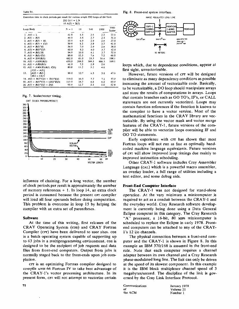
Table 111.
Execution time in clock periods per result for various simple DO loops of the form
DO 10 1 = 1.N I0 A(1) = B(1)
1000 Loop Body N = 1 10 100 1000
Scalar
1. A ( I ) = 1. 41.0 5.5 2.6 2.5 22.5 2. A(1) = B(I) 44.0 5.8 2.7 2.5 31.0 3. A( I ) = B(I) + 10. 55.0 6.9 2.9 2.6 37.0 4. A( I ) = B(I) + C(I) 59.0 8.2 3.9 3.7 41.0 5. A( I ) = B(/)*10. 56.0 7.0 2.9 2.6 38.0 6. A ( I ) = B(I)*C(I) 60.0 8.3 4.0 3.7 42.0 7. A( I ) = B(I) /IO. 94.0 10.8 4.1 3.7 52.0 8. A ( I ) = B(I ) /C(I ) 89.0 13.3 7.6 7.2 60.0 9. A(1) = SIN(B(I) ) 462.0 61.0 33.3 31.4 198.1
10. A(1) = A S I N ( B ( I ) ) 430.0 209.5 189.5 188.3 169.1 11. A(I ) = ABS(B( I ) ) 61.0 7.5 2.9 2.6 12. A(1) = A M A X I ( B ( I ) , C(I)) 80.0 11.2 5.2 4.8
[C(I) = A ( I ) ) 13. /A( / ) = a(I)~ 90.0 12'.7 6.3 518 47.0
LB(/) = CClJ 14. A(I ) = B(I)*C(I) + D(I)*E(I) 110.0 16.0 7.7 7.1 57.0 15. A(I ) = B(I)*C(I) + (D(I)*E(I)) 113.0 14.7 6.6 6.0 63.0 16. A( I ) = B( I ) 'C( I ) + D(I) 95.0 12.7 5.5 5.0 52.0
Fig. 7. Scalar/vector timing. COST (CLOCK PERIODS/RESULT)
3401t 3201[ 300 11 2801[ 260" m 240~n 220"IU 2001111 180 4111 160 " ~ cosALOG 140, SQRT 120,
EXP
- SCALAr' 80 ' VECTOR ~I 6?/ ; ( o ~ L ~ COS ALOG
SQRT EXP
1 10 20 30 40 50 60 64 VECTOR LENGTH
influence of chaining. For a long vector, the number of clock periods per result is approximately the number of memory references + 1. In loop 14, an extra clock period is consumed because the present cFr compiler will load all four operands before doing computation. This problem is overcome in loop 15 by helping the compiler with an extra set of parentheses.
Software At the time of this writing, first releases of the
CRAY Operating System (cos) and CRAY Fortran Compiler (cFr) have been delivered to user sites, cos is a batch operating system capable of supporting up to 63 jobs in a multiprogramming environment, cos is designed to be the recipient of job requests and data files from front-end computers. Output from jobs is normally staged back to the front-ends upon job com- pletion.
cFr is an optimizing Fortran compiler designed to compile ANSI 66 Fortran IV to take best advantage of the CRAY-I ' s vector processing architecture. In its present form, CFT will not attempt to vectorize certain
Fig. 8. Front-end system interface. PHASE MODULATED LONG LINE
i
70Xt06bps 64X106 bps IBM 370/168 datar te • 24X10~bp$
90 METERS
loops which, due to dependence conditions, appear at first sight, unvectorizable.
However , future versions of cFr will be designed to eliminate as many dependency conditions as possible increasing the amount of vectorizable code. Basically, to be vectorizable, a DO loop should manipulate arrays and store the results of computations in arrays. Loops that contain branches such as GO TO's, IF's, or CALL statements are not currently vectorized. Loops may contain function references if the function is known to the compiler to have a vector version. Most of the mathematical functions in the CRAY library are vec- torizable. By using the vector mask and vector merge features of the CRAY-1, future versions of the com- piler will be able to vectorize loops containing IF and GO TO statements.
Early experience with c ~ has shown that most Fortran loops will not run as fast as optimally hand- coded machine language equivalents. Future versions of c ~ will show improved loop timings due mainly to improved instruction scheduling.
Other CRAY-1 software includes Cray Assembler Language (CAL) which is a powerful macro assembler, an overlay loader, a full range of utilities including a text editor, and some debug aids.
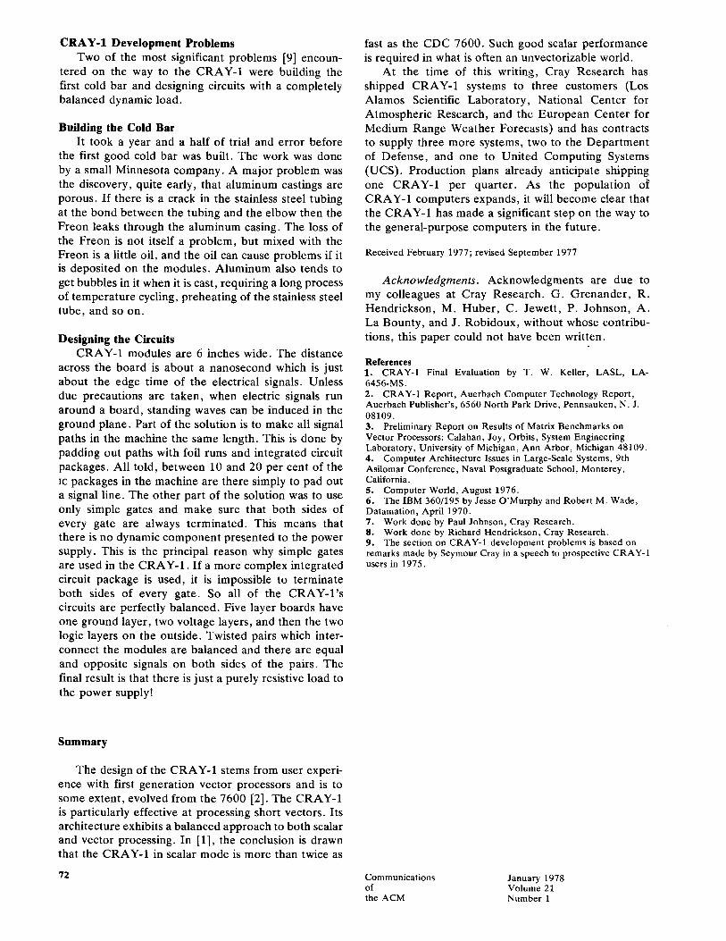
Front-End Computer Interface The CRAY-1 was not designed for stand-alone
operation. At the very minimum a minicomputer is required to act as a conduit between the CRAY-1 and the everyday world. Cray Research software develop- ment is currently being done using a Data General Eclipse computer in this category. The Cray Research " A " processor, a 16-bit, 80 MIPS minicomputer is scheduled to replace the Eclipse in early 1978. Front- end computers can be attached to any of the CRAY- l ' s 12 i/o channels.
The physical connection between a front-end com- puter and the C R A y o l is shown in Figure 8. In this example an IBM 370/168 is assumed in the front-end role. Note that each computer requires a channel adapter between its own channel and a Cray Research phase-modulated long line. The link can only be driven at the speed of its slowest component . In this example it is the IBM block multiplexer channel speed of 3 megabytes/second. The discipline of the link is gov- erned by the Cray Link Interface Protocol.
71 Communications January 1978 of Volume 21 the ACM Number I
CRAY-1 Development Problems Two of the most significant problems [9] encoun-
tered on the way to the CRAY-1 were building the first cold bar and designing circuits with a completely balanced dynamic load.
Building the Cold Bar It took a year and a half of trial and error before
the first good cold bar was built. The work was done by a small Minnesota company. A major problem was the discovery, quite early, that aluminum castings are porous. I f there is a crack in the stainless steel tubing at the bond between the tubing and the elbow then the Freon leaks through the aluminum casing. The loss of the Freon is not itself a problem, but mixed with the Freon is a little oil, and the oil can cause problems if it is deposited on the modules. Aluminum also tends to get bubbles in it when it is cast, requiring a long process of tempera ture cycling, preheating of the stainless steel tube, and so on.
Designing the Circuits CRAY-1 modules are 6 inches wide. The distance
across the board is about a nanosecond which is just about the edge time of the electrical signals. Unless due precautions are taken, when electric signals run around a board, standing waves can be induced in the ground plane. Part of the solution is to make all signal paths in the machine the same length. This is done by padding out paths with foil runs and integrated circuit packages. All told, between 10 and 20 per cent of the IC packages in the machine are there simply to pad out a signal line. The other part of the solution was to use only simple gates and make sure that both sides of every gate are always terminated. This means that there is no dynamic component presented to the power supply. This is the principal reason why simple gates are used in the CRAY-1 . I f a more complex integrated circuit package is used, it is impossible to terminate both sides of every gate. So all of the C R A Y - I ' s circuits are perfectly balanced. Five layer boards have one ground layer, two voltage layers, and then the two logic layers on the outside. Twisted pairs which inter- connect the modules are balanced and there are equal and opposite signals on both sides of the pairs. The final result is that there is just a purely resistive load to the power supply!
fast as the CDC 7600. Such good scalar performance is required in what is often an unvectorizable world.
At the time of this writing, Cray Research has shipped CRAY-1 systems to three customers (Los Alamos Scientific Labora tory , National Center for Atmospher ic Research, and the European Center for Medium Range Weather Forecasts) and has contracts to supply three more systems, two to the Depar tment of Defense, and one to United Computing Systems (UCS). Production plans already anticipate shipping one CRAY-1 per quarter . As the populat ion o~ CRAY-1 computers expands, it will become clear that the CRAY-1 has made a significant step on the way to the general-purpose computers in the future.
Received February 1977; revised September 1977
Acknowledgments. Acknowledgments are due to my colleagues at Cray Research. G. Grenander , R. Hendrickson, M. Huber , C. Jewett , P. Johnson, A. La Bounty, and J. Robidoux, without whose contribu- tions, this paper could not have been written.
References 1. CRAY-1 Final Evaluation by T. W. Keller, LASL, LA- 6456-MS. 2. CRAY-1 Report, Auerbach Computer Technology Report, Auerbach Publisher's, 6560 North Park Drive, Pennsauken, N. J. 08109. 3. Preliminary Report on Results of Matrix Benchmarks on Vector Processors: Calahan, Joy, Orbits, System Engineering Laboratory, University of Michigan, Ann Arbor, Michigan 48109. 4. Computer Architecture Issues in Large-Scale Systems, 9th Asilomar Conference, Naval Postgraduate School, Monterey, California. 5. Computer World, August 1976. 6. The IBM 360/195 by Jesse O'Murphy and Robert M. Wade, Datamation, April 1970. 7. Work done by Paul Johnson, Cray Research. 8. Work done by Richard Hendrickson, Cray Research. 9. The section on CRAY-1 development problems is based on remarks made by Seymour Cray in a speech to prospective CRAY-1 users in 1975.
Summary
The design of the CRAY-1 stems f rom user experi- ence with first generation vector processors and is to some extent, evolved f rom the 7600 [2]. The CRAY-1 is particularly effective at processing short vectors. Its architecture exhibits a balanced approach to both scalar and vector processing. In [1], the conclusion is drawn that the CRAY-1 in scalar mode is more than twice as
72 Communications January 1978 of Volume 21 the ACM Number 1