Embed Size (px)
Citation preview
EECS 100 Lab Guide Bharathwaj Muthuswamy
The Operational Amplfier Lab Guide
COMPONENTS REQUIRED FOR THIS LAB :1. LM741 op-amp integrated circuit (IC)
2. 1k resistors 3. 10k resistor 4. Wires, wire cutters and breadboard
1. Introduction
So far in this course you have been dealing with circuits that do not amplify the voltageinput. That is, the voltages in the circuit are either equal to or less than the input voltage.In this lab, you are going to be introduced to the voltage amplifier – a circuit elementthat outputs voltage that is greater than or equal to the input voltage. There is anexception to this rule called railing that we will talk about later.
Mathematically, if the input to an amplifier is:
V � � sin 2 � f t volts (1)
the output may be something like:
V o� 5sin 2 � f t volts (2)
The amplifier you will be using is also an operational amplifier – you can use the deviceto perform common math operations like integration and differentiation. However, youwill not be dealing with those operations in this lab, you will just be examining theamplifier functionality.
Operational amplifiers (op-amps) were first developed by George Philbrick when he wasan employee for the National Defense Research Council in the early 1940s [1]. The op-amp later went through many transitions, Fairchild Semiconductor corp. developed a de-facto standard in 1962 – the µ741 [1]. This op-amp has lived on for over forty years andyou will be using this op-amp in the lab. From now, on whenever I say “op-amp” thinkthe µ741.
We mentioned that op-amps can be used to build circuits that perform mathematicaloperations and amplify voltage. Op-amps can also be used to build circuits that performAnalog-to-Digital (A/D) conversion, square-wave generators (oscillators) and a wholebunch of other stuff. The robustness of the op-amp is because the functionality of the op-amp can be extended by the use of feedback. Although a detailed description of feedbackis beyond the scope of this guide, we will give you enough information to appreciate theusefulness of feedback. But first, let us look at the circuit symbol of the op-amp.
2. The Differential Amplifier
i. Circuit symbol and model
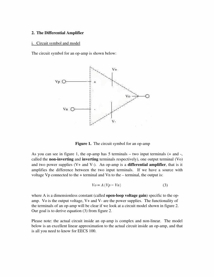
The circuit symbol for an op-amp is shown below:
Figure 1. The circuit symbol for an op-amp
As you can see in figure 1, the op-amp has 5 terminals – two input terminals (+ and -,called the non-inverting and inverting terminals respectively), one output terminal (Vo)and two power supplies (V+ and V-). An op-amp is a differential amplifier, that is itamplifies the difference between the two input terminals. If we have a source withvoltage Vp connected to the + terminal and Vn to the – terminal, the output is:
Vo � A Vp � Vn (3)
where A is a dimensionless constant (called open-loop voltage gain) specific to the op-amp. Vo is the output voltage, V+ and V- are the power supplies. The functionality ofthe terminals of an op-amp will be clear if we look at a circuit model shown in figure 2.Our goal is to derive equation (3) from figure 2.
Please note: the actual circuit inside an op-amp is complex and non-linear. The modelbelow is an excellent linear approximation to the actual circuit inside an op-amp, and thatis all you need to know for EECS 100.
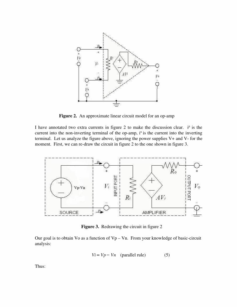
Figure 2. An approximate linear circuit model for an op-amp
I have annotated two extra currents in figure 2 to make the discussion clear. ip is thecurrent into the non-inverting terminal of the op-amp, in is the current into the invertingterminal. Let us analyze the figure above, ignoring the power supplies V+ and V- for themoment. First, we can re-draw the circuit in figure 2 to the one shown in figure 3.
Figure 3. Redrawing the circuit in figure 2
Our goal is to obtain Vo as a function of Vp – Vn. From your knowledge of basic-circuitanalysis:
Vi � Vp � Vn (parallel rule) (5)
Thus:
Vo AVi A Vp Vn (output is open, no current flows through Ro) (6)
If we graph Vo as a function of Vp-Vn, we get the Voltage Transfer Characteristic(VTC) of an op-amp, as shown below:
Figure 4. Ideal VTC of an op-amp
The graph shows that Vo varies linearly as a function of Vp-Vn1. This should be obviousfrom equation 6 since A is a constant. In reality, we all know that you cannot get infinitegain – the amplifier cannot amplify if we input a trillion volts. This is where thefunctionality of the power supplies comes into play. A real op-amp will have a VTCshown below:
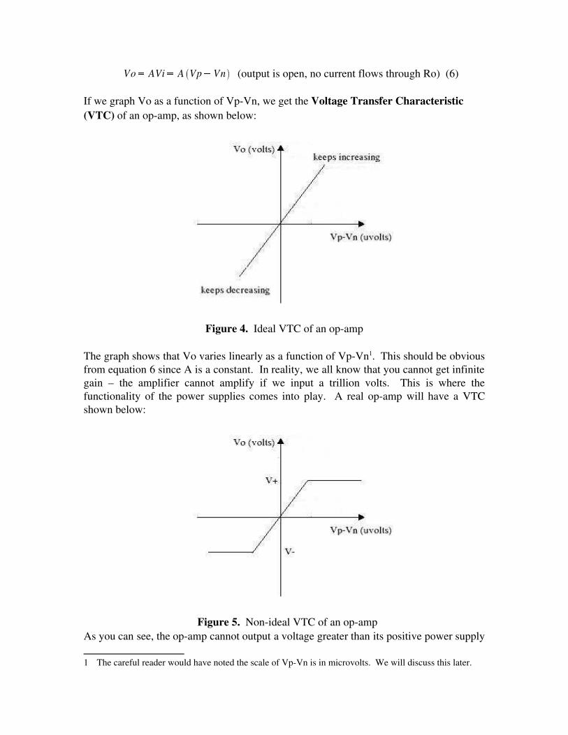
Figure 5. Non-ideal VTC of an op-ampAs you can see, the op-amp cannot output a voltage greater than its positive power supply
1 The careful reader would have noted the scale of Vp-Vn is in microvolts. We will discuss this later.
(V+) or lower than its negative power supply (V-), a phenomenon called railing.Remember this when you use an op-amp. In this lab, your V+ is set to +10 V and V- to-10 V as shown in the figure below.
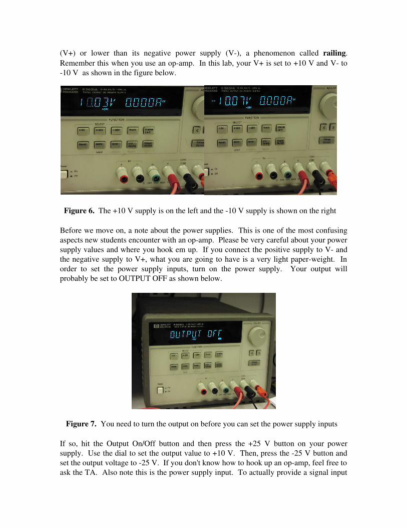
Figure 6. The +10 V supply is on the left and the -10 V supply is shown on the right
Before we move on, a note about the power supplies. This is one of the most confusingaspects new students encounter with an op-amp. Please be very careful about your powersupply values and where you hook em up. If you connect the positive supply to V- andthe negative supply to V+, what you are going to have is a very light paper-weight. Inorder to set the power supply inputs, turn on the power supply. Your output willprobably be set to OUTPUT OFF as shown below.
Figure 7. You need to turn the output on before you can set the power supply inputs
If so, hit the Output On/Off button and then press the +25 V button on your powersupply. Use the dial to set the output value to +10 V. Then, press the -25 V button andset the output voltage to -25 V. If you don't know how to hook up an op-amp, feel free toask the TA. Also note this is the power supply input. To actually provide a signal input
to the op-amp you are going to be using the function generator. More on this when wetalk about the actual experiment setup.
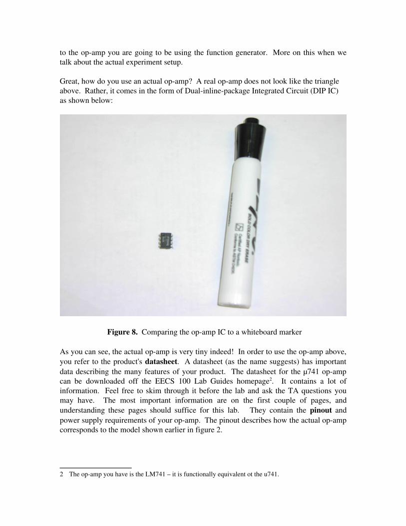
Great, how do you use an actual op-amp? A real op-amp does not look like the triangleabove. Rather, it comes in the form of Dual-inline-package Integrated Circuit (DIP IC)as shown below:
Figure 8. Comparing the op-amp IC to a whiteboard marker
As you can see, the actual op-amp is very tiny indeed! In order to use the op-amp above,you refer to the product's datasheet. A datasheet (as the name suggests) has importantdata describing the many features of your product. The datasheet for the µ741 op-ampcan be downloaded off the EECS 100 Lab Guides homepage2. It contains a lot ofinformation. Feel free to skim through it before the lab and ask the TA questions youmay have. The most important information are on the first couple of pages, andunderstanding these pages should suffice for this lab. They contain the pinout andpower supply requirements of your op-amp. The pinout describes how the actual op-ampcorresponds to the model shown earlier in figure 2.
2 The op-amp you have is the LM741 – it is functionally equivalent ot the u741.
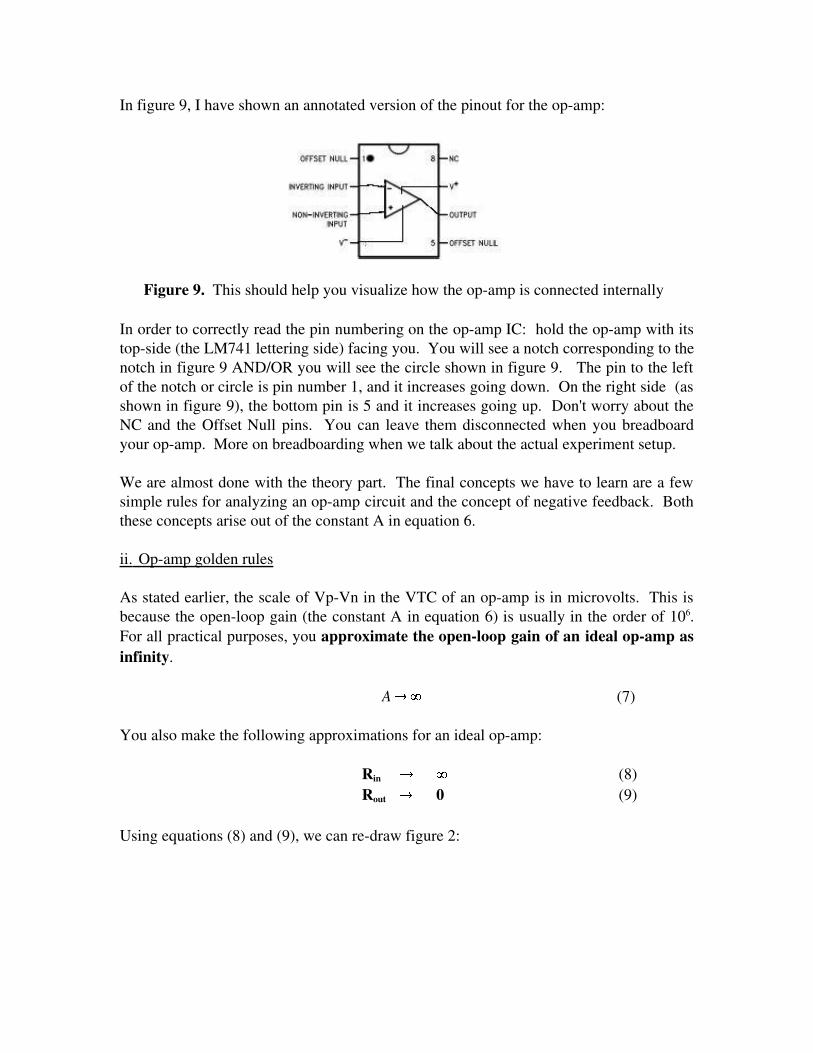
In figure 9, I have shown an annotated version of the pinout for the op-amp:
Figure 9. This should help you visualize how the op-amp is connected internally
In order to correctly read the pin numbering on the op-amp IC: hold the op-amp with itstop-side (the LM741 lettering side) facing you. You will see a notch corresponding to thenotch in figure 9 AND/OR you will see the circle shown in figure 9. The pin to the leftof the notch or circle is pin number 1, and it increases going down. On the right side (asshown in figure 9), the bottom pin is 5 and it increases going up. Don't worry about theNC and the Offset Null pins. You can leave them disconnected when you breadboardyour op-amp. More on breadboarding when we talk about the actual experiment setup.
We are almost done with the theory part. The final concepts we have to learn are a fewsimple rules for analyzing an op-amp circuit and the concept of negative feedback. Boththese concepts arise out of the constant A in equation 6.
ii. Op-amp golden rules
As stated earlier, the scale of Vp-Vn in the VTC of an op-amp is in microvolts. This isbecause the open-loop gain (the constant A in equation 6) is usually in the order of 106.For all practical purposes, you approximate the open-loop gain of an ideal op-amp asinfinity.
A � � (7)
You also make the following approximations for an ideal op-amp:
Rin � � (8) Rout � 0 (9)
Using equations (8) and (9), we can re-draw figure 2:
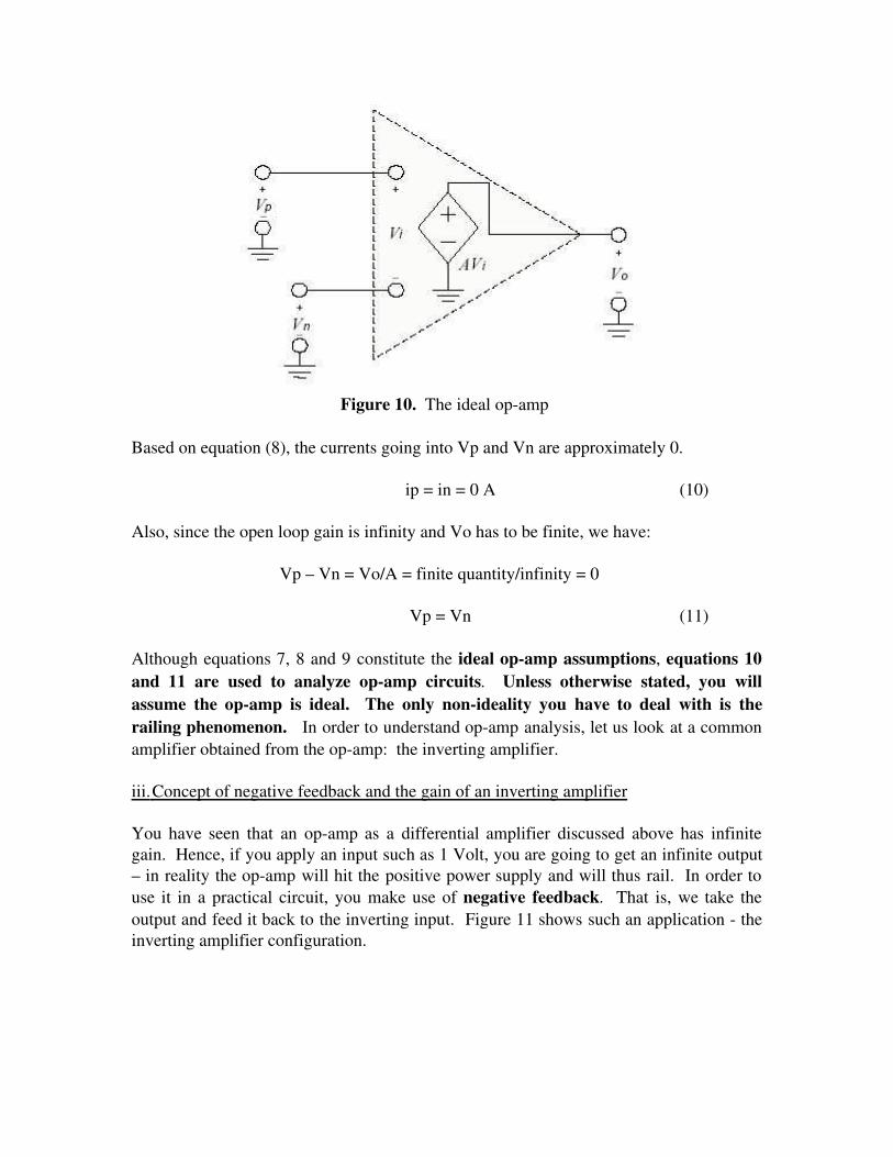
Figure 10. The ideal op-amp
Based on equation (8), the currents going into Vp and Vn are approximately 0.
ip = in = 0 A (10)
Also, since the open loop gain is infinity and Vo has to be finite, we have:
Vp – Vn = Vo/A = finite quantity/infinity = 0
Vp = Vn (11)
Although equations 7, 8 and 9 constitute the ideal op-amp assumptions, equations 10and 11 are used to analyze op-amp circuits. Unless otherwise stated, you willassume the op-amp is ideal. The only non-ideality you have to deal with is therailing phenomenon. In order to understand op-amp analysis, let us look at a commonamplifier obtained from the op-amp: the inverting amplifier.
iii. Concept of negative feedback and the gain of an inverting amplifier
You have seen that an op-amp as a differential amplifier discussed above has infinitegain. Hence, if you apply an input such as 1 Volt, you are going to get an infinite output– in reality the op-amp will hit the positive power supply and will thus rail. In order touse it in a practical circuit, you make use of negative feedback. That is, we take theoutput and feed it back to the inverting input. Figure 11 shows such an application - theinverting amplifier configuration.

Figure 11. The inverting amplifier circuit
Noitce how the output is connected to the inverting input through R2. A detaileddiscussion of feedback is beyond the scope of this guide. However, a qualitative idea canbe obtained by looking at equation 6:
Vo � A Vp � Vn
Assume R2 = 0 in figure 11. Then, we get:
Vo � A Vp � Vo
The equation above is a recursive equation. As you all know, A is huge (tends towardsinfinity for an ideal op-amp). Hence, Vp = Vo. Suppose Vo increases a little bit. Then,Vp < Vo now and A(Vp-Vo) < 0 since A is positive. Hence, if Vo tries to increase thenegative feedback immediately3 causes Vp to move towards Vn, thereby stabilizing thecircuit.
Let us go back to figure 11 and assume R2 is not zero. We want Vo as a function Vin inthe circuit in figure 11 and obviously this is not going to be equation 3 because of thenegative feedback. The corresponding gain we are going to get is called the closed-loopgain4of the op-amp.
In order to derive the closed-loop gain, let us start with equation 10. From equation 10,we know the current into the inverting input is zero. Hence, by applying KCL at theinverting input, the current I flowing through R2 in figure 11 is the same current whichflows through R1:
I = IR1
Applying Ohm's law:
3 In an actual circuit, there is obviously some delay between a change in Vo and the negative feedbacktaking effect. We can safely neglect this effect in our case.
4 It is called a “closed loop gain” because you have a loop from the output to the inverting input.
Vo � Vn
R2��� Vin
R1 (12)
From equation 11, we know:
Vp = Vn = 0 (since Vp is grounded)
Substituting the value of Vn in (12) and rearranging:
Vo �� R2R1
Vin (13)
The quantity within paranthesis in equation 13 is the closed loop gain for the invertingamplifier. This is awesome – by using negative feedback you eliminated the dependenceof gain on A and designed the gain of the op-amp to depend only on R2 and R1.Obviously, you can now control the gain of an op-amp using only two resistors. If R2 istwice the value of R1, you get two times the gain and so on. The gain is negative, youwill design an amplifier with positive gain in the prelab. In summary, for analyzing acircuit with an op-amp in negative feedback:
1. Use equation (10) and KCL at the inverting and/or non-inverting inputs.2. Use equation (11) to eliminate the value of Vp or Vn.
Please note that (1) and (2) are not hard-and-fast rules. They just serve as a guide – usethem wisely!
As a concluding remark to this section, what happens when you feedback Vo to the non-inverting input? Turns out you get positive feedback. By using the same qualitativerecursion argument above, you can show that positive feedback leads the circuit towardsinstability. This is not useless – you use positive feedback to make square wavegenerators and other kinds of oscillators. You will see how to build a square wavegenerator in a later lab.
Thats all for the theory! Now, its your turn. Before we go on to the experiment, youshould finish the prelab.
3. The Experiment
The TA will demonstrate how to wire the op-amp using the breadboard. PLEASENOTE: WIRE NEATLY! THIS IS THE MAGIC ASPIRIN THAT WILLREDUCE A LOT OF HEADACHE WILL DEBUGGING.
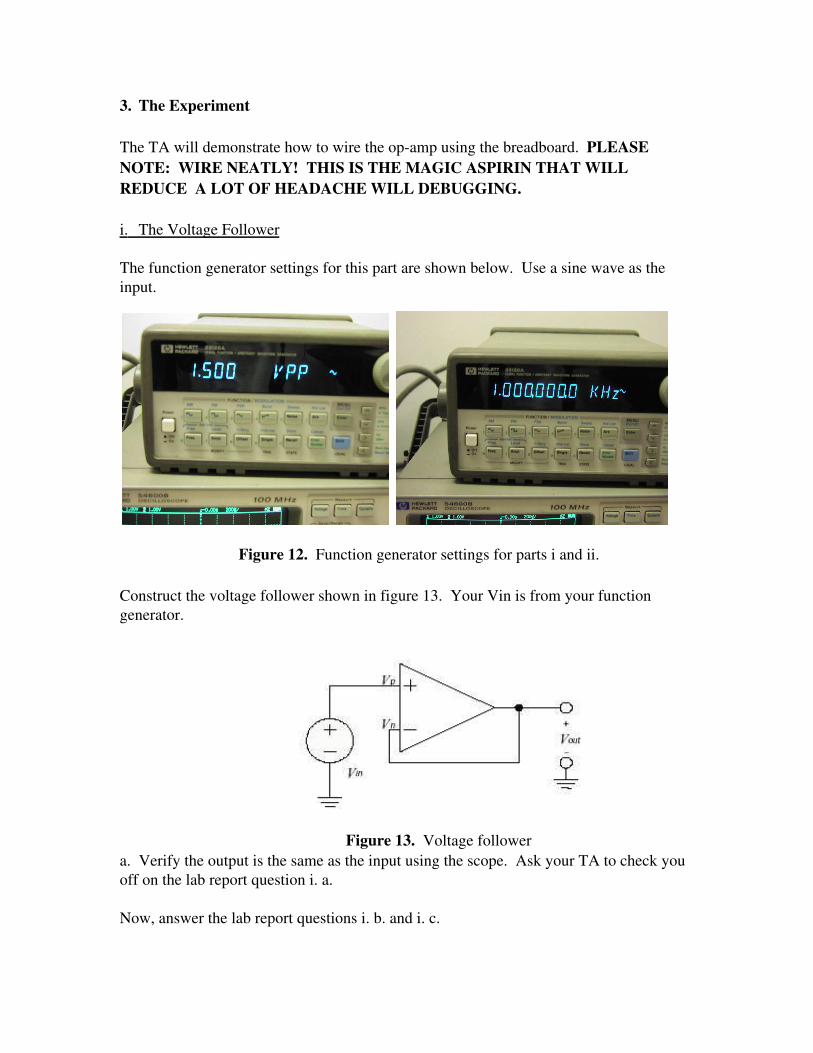
i. The Voltage Follower
The function generator settings for this part are shown below. Use a sine wave as theinput.
Figure 12. Function generator settings for parts i and ii.
Construct the voltage follower shown in figure 13. Your Vin is from your functiongenerator.
Figure 13. Voltage followera. Verify the output is the same as the input using the scope. Ask your TA to check youoff on the lab report question i. a.
Now, answer the lab report questions i. b. and i. c.
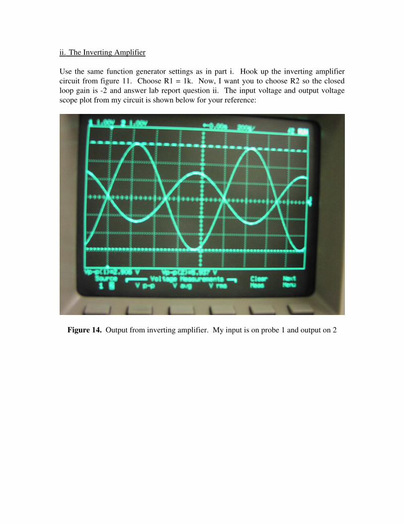
ii. The Inverting Amplifier
Use the same function generator settings as in part i. Hook up the inverting amplifiercircuit from figure 11. Choose R1 = 1k. Now, I want you to choose R2 so the closedloop gain is -2 and answer lab report question ii. The input voltage and output voltagescope plot from my circuit is shown below for your reference:
Figure 14. Output from inverting amplifier. My input is on probe 1 and output on 2
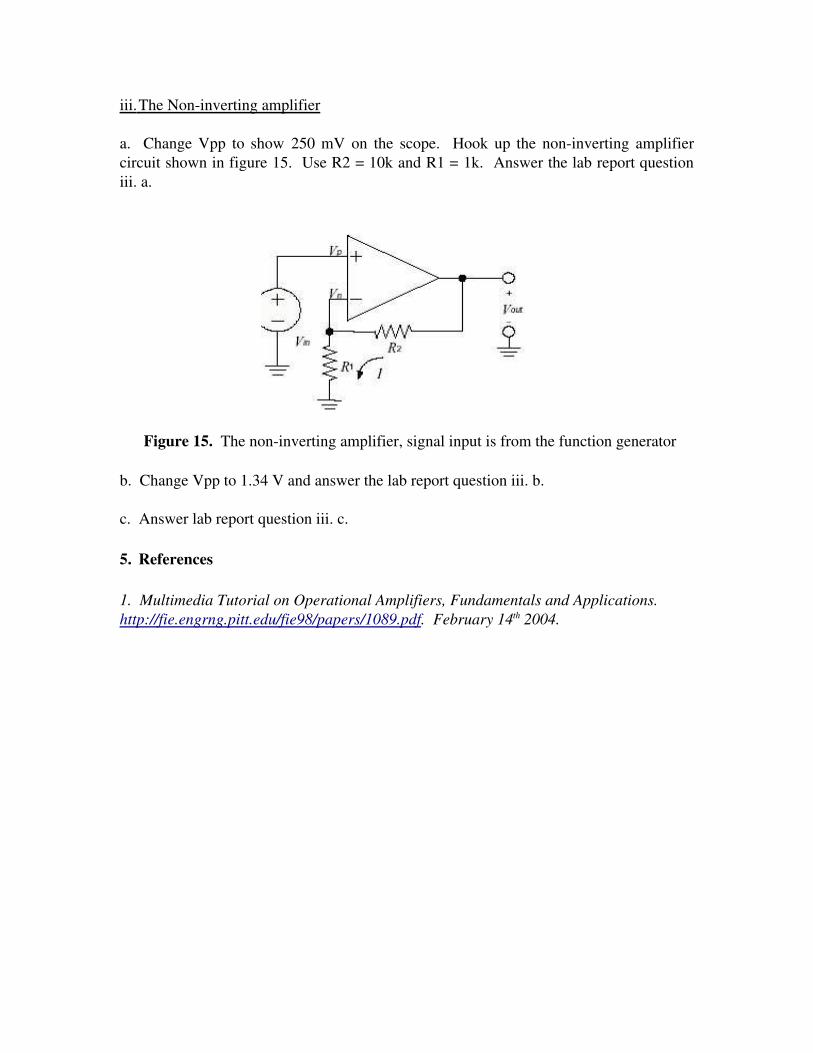
iii. The Non-inverting amplifier
a. Change Vpp to show 250 mV on the scope. Hook up the non-inverting amplifiercircuit shown in figure 15. Use R2 = 10k and R1 = 1k. Answer the lab report questioniii. a.
Figure 15. The non-inverting amplifier, signal input is from the function generator
b. Change Vpp to 1.34 V and answer the lab report question iii. b.
c. Answer lab report question iii. c.
5. References
1. Multimedia Tutorial on Operational Amplifiers, Fundamentals and Applications.http://fie.engrng.pitt.edu/fie98/papers/1089.pdf. February 14th 2004.


![[LAB 5] OPERATIONAL AMPLIFIER.pdf](https://img.pdfslide.net/doc/110x75/577c77801a28abe0548c5c99/lab-5-operational-amplifierpdf.jpg)