Embed Size (px)
Citation preview
This content has been downloaded from IOPscience. Please scroll down to see the full text.
Download details:
IP Address: 134.99.128.41
This content was downloaded on 28/11/2013 at 19:10
Please note that terms and conditions apply.
The optical properties of amorphous and crystalline germanium
View the table of contents for this issue, or go to the journal homepage for more
1976 J. Phys. C: Solid State Phys. 9 4335
(http://iopscience.iop.org/0022-3719/9/23/018)
Home Search Collections Journals About Contact us My IOPscience
J. Phys. C : Solid State Phys., Vol. 9, 1976. Printed in Great Britain. @ 1976
The optical properties of amorphous and crystalline germanium
S G Tomlin, E Khawaja-f and G K M ThutupalliS Physics Department, University of Adelaide, S Australia
Received 10 May 1976
Abstract. A detailed study has been made of Tomlin’s method of determining the optical constants of an absorbing specimen by measuring the normal-incidence reflectances from the specimen itself and when coated with a thin transparent layer. It has been applied successfully to the measurement of the optical properties of amorphous and crystalline germanium in the spectral range from 700 to 300 MI where specimens are highly absorbing. For thin films it has thus been possible to extend the range previously covered by the reflectance and transmit- tance measurements of Denton and Tomlin.
The absorption of the amorphous thin films near the absorption edge has been re- examined and it is shown that four band gaps may be recognized, for which an interpretation in terms of a Mott-Davis (1971) model is offered.
The extension of direct measurements of n and k into the absorbing region allows for interesting comparisons with results based on Kramers-Kronig analysis of reflectance data, and is found to yield some information not found by the latter method.
1. Introduction
The optical constants of highly absorbing materials have usually been found by measuring reflectance, at normal incidence, over a wide range of wavelengths and using Kramers- Kronig analysis. The difficulties inherent in this procedure are well known and may lead to uncertainties in the results (Tauc and Abraham 1969, Seraphin and Bennett 1967, Connell et a1 1973). A method which avoids these problems, while retaining the advan- tages of measurements of reflectance at normal incidence, has been described by Tomlin (1972) who, after writing his paper, found that a similar experimental procedure for use in the infrared region had been devised by Vincent-Geisse (1964, also Vincent-Geisse et a1 1967). Both methods require the evaporation of thin transparent films onto the absorbing specimen and the measurement, at normal incidence, of reflectances R and R , from the surface of the specimen itself and from the coated surface, respectively. The methods differ in the treatment of the data, particularly the extension of the Tomlin method to be discussed here.
The first purpose of this paper is to examine more fully the solution of the equations from which the refractive index n and absorption index k of the specimen may be cal- culated from the two measured reflectances R and R,. It will be shown that the thickness of the applied film can be determined accurately from the criterion that the dispersion curve should be continuous, in much the same way as in the procedure for finding the
t On leave from the Pakistan Atomic Energy Commission, Islamabad, Pakistan. 1 On leave from Vikram Sarabhai Space Centre, Trivandrum, India.
4335
4336 S G Tomlin, E Khawaja and G K M Thutupalli
optical constants of transparent or semi-transparent films described by Denton et ul (1972), and that ambiguity due to multiple solutions can be avoided.
Secondly, an account is given of the application of this method to the determination of n and k for amorphous Ge films in the absorbing region from 700 to 300 nm, and for bulk polycrystalline and single-crystal specimens of Ge in the region from 1750 to 300 nm, using a film of tantalum pentoxide evaporated onto the Ge.
These results for amorphous Ge extend the measurements of Denton and Tomlin (1972) from 2000 down to 300 nm, and a new analysis of the absorption near the absorp- tion edge is presented and discussed in terms of a Mott-Davis model of the energy levels in amorphous materials.
Also, the results over the whole range covered are compared with those of other workers obtained from Kramers-Kronig analysis of reflectance data.
2. Discussion of the method
The reflectance of an absorbing specimen, which mai be either a bulk sample suitably polished or an evaporated film with sufficient absorption to eliminate any effects of multiple reflection in it, is given by
(n2 - no), + k: (n, + no)’ + k: R =
where no is the refractive index of air and n2 - ik, is the complex refractive index of the material.
The reflectance from the same specimen coated with a transparent film of refractive index n, is given by (Tomlin 1965)
1 - 1 + R ,
1 - R , 4nonfn, {(n; + n f ) ( n f + n: + k:) + (ni - n:)[(nf - n: - ki)cos2y,
+ 2n,k, sin 2y,]) (2)
where y , = 2nn,d,/A, d , is the film thickness and A the wavelength. A graphical solution of these equations may be obtained by writing equation ( 1 ) to
represent a circle in the n,, k, plane, and obtaining a linear relation between 12, and k, from equations ( 1 ) and (2). Solutions for n2 and k, are then given by the intersection of the straight line and circle (Tomlin 1972).
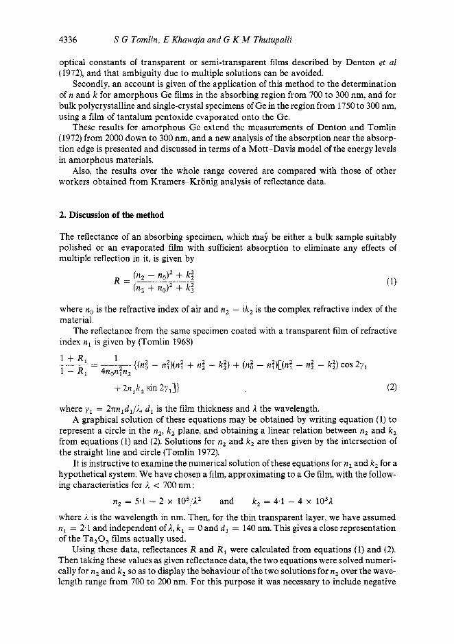
It is instructive to examine the numerical solution of these equations for n, and k, for a hypothetical system. We have chosen a film, approximating to a Ge film, with the follow- ing characteristics for /z < 700 nm :
and
where /z is the wavelength in nm. Then, for the thin transparent layer, we have assumed n, = 2.1 and independent of A, k, = 0 and d , = 140 nm. This gives a close representation of the Ta,05 films actually used.
Using these data, reflectances R and R , were calculated from equations ( 1 ) and (2). Then taking these values as given reflectance data, the two equations were solved numeri- cally for n2 and k, so as to display the behaviour of the two solutions for n, over the wave- length range from 700 to 200 nm. For this purpose it was necessary to include negative
n, = 5.1 - 2 x 10⁵/A2 k, = 4.1 - 4 x 10³A
The optical properties of amorphous and crystalline germanium 4337
values of k , in the computations to ensure the determination of all possible values of n2. Details of the computing procedure have been given by Khawaja (1975). The results of such a calculation are shown in figure 1, which reproduces the initially assumed disper- sion curve and shows the inadmissible second solution.
Wavelength ( n m )
Figure 1. Solution of equations (1) and (2) for the hypothetical system described in the text.
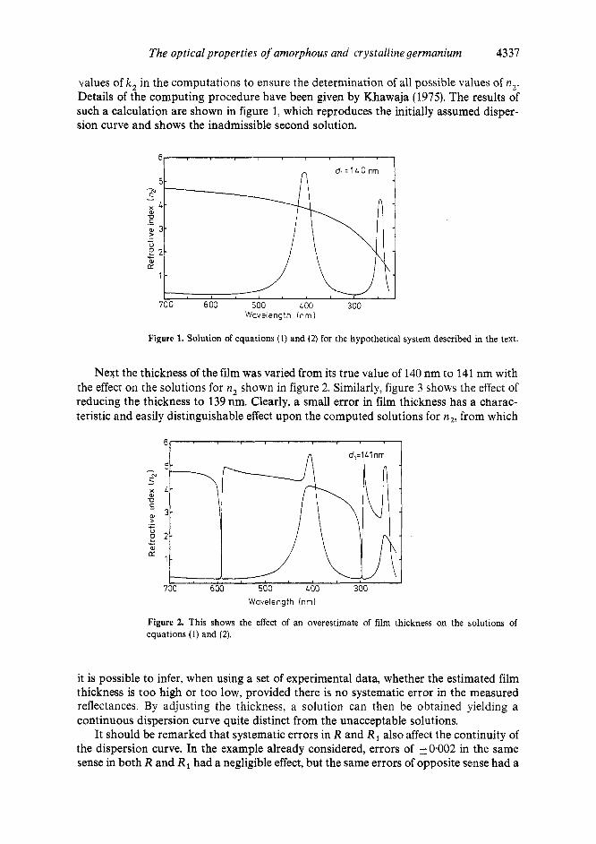
Next the thickness of the film was varied from its true value of 140 nm to 1.41 nm with the effect on the solutions for n, shown in figure 2. Similarly, figure 3 shows the effect of reducing the thickness to 139 nm. Clearly, a small error in film thickness has a charac- teristic and easily distinguishable effect upon the computed solutions for n2, from which
wavelength (nm)
Figure 2. This shows the effect of an overestimate of film thickness on the solutions of equations (1) and (2).
it is possible to infer, when using a set of experimental data, whether the estimated film thickness is too high or too low, provided there is no systematic error in the measured reflectances. By adjusting the thickness, a solution can then be obtained yielding a continuous dispersion curve quite distinct from the unacceptable solutions.
It should be remarked that systematic errors in R and R I also affect the continuity of the dispersion curve. In the example already considered, errors of 40.002 in the same sense in both R and R I had a negligible effect, but the same errors of opposite sense had a
4338 S G Tomlin, E Khawaja and G K M Thutupalli
0.6-
0.5
8 0,L-
: 5 03-
d - a, L
0.1
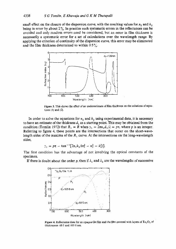
small effect on the closure of the dispersion curve, with the resulting values for n2 and k, being in error by about 2 %. In practice such systematic errors in the reflectances can be avoided and only random errors need be considered, but an error in film thickness is necessarily a systematic error for a set of calculations over the wavelength range. By applying the criterion of continuity of the dispersion curve, this error may be eliminated and the film thickness determined to within 0.5 %.
...... . , . . Ta,GS/Ge f i lm , . ......... :' , . . , : ' '
,:'Ft, . .
.. ;.. , , . . '1. ' ' . . . . , R , . . . . . . . . . :,:: . . . . . . . .. , -
. .
:al -1058 nm ,
:R,
. :'&=685nm . . .. '
- c" 51-----4 i \ i
Wavelength (nm)
Figure 3. This shows the effect of an underestimate of film thickneF on the solutions of equa- tions (1) and (2).
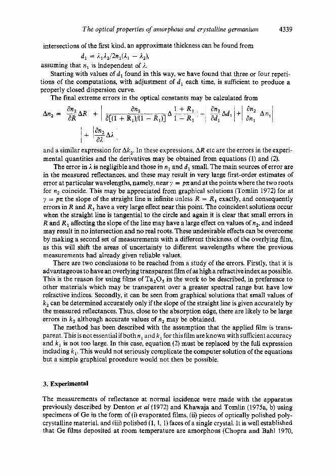
In order to solve the equations for n2 and k, using experimental data, it is necessary to have an estimate of the thickness dl as a starting point. This may be obtained from the condition (Tomlin 1972) that R 1 = R when y1 = 2nn1d1/ll = pn, where p is an integer. Referring to figure 4, these points are the intersections that occur on the short-wave- length sides of the maxima of the R I curve. At the intersections on the long-wavelength sides,
y1 = pn - tan-'[2nlk,/(n? - n$ - k$)].
The first condition has the advantage of not involving the optical constants of the specimen.
If there is doubt about the order p , then if ll1 and 112 are the wavelengths of successive
The optical properties of amorphous and crystulline germanium 4339
intersections of the first kind, an approximate thickness can be found from
assuming that n, is independent of 1. Starting with values of d , found in this way, we have found that three or four repeti-
tions of the computations, with adjustment of d , each time, is sufficient to produce a properly closed dispersion curve.
di = I112/2n1(3L1 -
The final extreme errors in the optical constants may be calculated from
and a similar expression for Ak,. In these expressions, AR etc are the errors in the experi- mental quantities and the derivatives may be obtained from equations (1) and (2).
The error in I is negligible and those in n, and d , small. The main sources of error are in the measured reflectances, and these may result in very large first-order estimates of error at particular wavelengths, namely, near y = pn: and at the points where the two roots for n2 coincide. This may be appreciated from graphical solutions (Tomlin 1972) for at y = pn the slope of the straight line is infinite unless R = R , exactly, and consequently errors in R and R I have a very large effect near this point. The coincident solutions occur when the straight line is tangential to the circle and again it is clear that small errors in R and R , affecting the slope of the line may have a large effect on values of n,, and indeed may result in no intersection and no real roots. These undesirable effects can be overcome by making a second set of measurements with a different thickness of the overlying film, as this will shift the areas of uncertainty to different wavelengths where the previous measurements had already given reliable values.
There are two conclusions to be reached from a study of the errors. Firstly, that it is advantageous to have an overlying transparent film of as high a refractive index as possible. This is the reason for using films of Ta,O, in the work to be described, in preference to other materials which may be transparent over a greater spectral range but have low refractive indices. Secondly, it can be seen from graphical solutions that small values of k, can be determined accurately only if the slope of the straight line is given accurately by the measured reflectances. Thus, close to the absorption edge, there are likely to be large errors in k, although accurate values of n2 may be obtained.
The method has been described with the assumption that the applied film is trans- parent. This is not essential if both n1 and k , for this film are known with sufficient accuracy and k , is not too large. In this case, equation (2) must be replaced by the full expression including k l . This would not seriously complicate the computer solution of the equations but a simple graphical procedure would not then be possible.
3. Experimental
The measurements of reflectance at normal incidence were made with the apparatus previously described by Denton et al(l972) and Khawaja and Tomlin (1975a, b) using specimens of Ge in the form of (i) evaporated films, (ii) pieces of optically polished poly- crystalline material, and (iii) polished (1,1, 1) faces of a single crystal. It is well established that Ge films deposited at room temperature are amorphous (Chopra and Bahl 1970,
4340 S G Tomlin, E Khawaja and G K M Thutupalli
Paul et a1 1973). Following Chopra and Bahl, who emphasize the need for electron microscopy to establish the presence or absence of microcrystallites, we found no sign of' any such crystallinity in any of the films used in this work. It was concluded that all films were amorphous, including those deposited at room temperature and annealed for 3 h at 300"C, in agreement with the findings of Paul et al(1973). X-ray diffraction patterns con- firmed this conclusion.
Ta,O, and ZrO, have both been used for the transparent overlying layer but the results reported here will refer only to the use of the former. This proved to be more con- venient, for the Ta205 films were amorphous with smooth surfaces while the ZrO, films were polycrystalline and rough (Khawaja and Tomlin 1975b), and with rough films it is necessary to take the roughness into account by using the much more complicated formulae for a double layer on a substrate. It is quite feasible to do this, and measurements made with ZrO, have been found to be in good agreement with those using Ta,05 (Khawaja 1975).
Specimens in the form of evaporated films were prepared by evaporating Ge from a conical tungsten basket, in a vacuum of lo-' Torr, onto quartz substrates at room temperature. A magnetically operated shutter above the source allowed outgassing of the Ge prior to deposition at the rate of 20-40 nm per minute. For measurements in the low- absorption range from 2000 to 700 nm, films of thickness 100-300 nm were prepared. Films thicker than 250 nm were used for measurements in the highly absorbing region from 700 to 300nm to ensure that there were no appreciable effects due to multiple reflections in the Ge. Pairs of such films were deposited simultaneously and then exposed to air. One was coated with Ta205 by sputtering, as described by Khawaja and Tomlin (1975b). During this process, which occupied 20-40 min, the Ge film reached a tempera- ture of about 300°C. To ensure that the pairs of Ge films had similar properties, the un- coated films were annealed in vacuum at 300°C for 30 min. Then the reflectances R and R , were measured with the specimens in air at room temperature.
Specimens of polycrystalline Ge of dimensions 2.5 x 3.75 x 0.2 cm3 were cut from a piece of high-purity material obtained from Rofm Ltd, England. The faces were ground with successively finer grades of diamond abrasive and finally polished with A1203 polishing powder on a beeswax lap. The reflectances R from four such surfaces were measured over the spectral range 1750-250 nm. The variation in R from face to face was less than 0.004. The surfaces were then coated with Ta,05 layers of from 100 to 270 nm thickness, and the reflectances R , measured over the same range. The upper wavelength limit was such that the Ge specimen transmittance was less than 1 %, so that measured reflectances were not appreciably affected by multiple reflection in it. The lower limit was fixed by the onset of absorption in the Ta,05.
The single-crystal specimen of Ge, 2.5 cm in diameter and 0.3 cm thick, was cut on a (1, 1, 1) face and polished in the same way as the polycrystalline material.
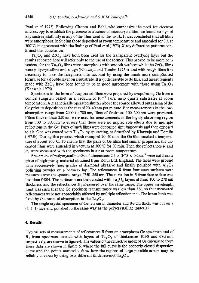
4. Results
Typical sets of measurements of reflectances R from an amorphous Ge specimen and of R , from specimens coated with layers of Ta,O, of thicknesses 1054 and 68*5nm, respectively, are shown in figure 4. The values of the refractive index of Ge calculated from these data are shown in figure 5, where the full curve is the properly closed dispersion curve and the points marked x show how the regions of large possible errors may be reliably covered by using two different thicknesses of Ta,O,.
The optical properties of amorphous and crystalline germanium 434 1
Wavelength lnml
Figure 5. The solution for the refractive index of amorphous Ge from the data of figure 4, with the Ta,O, layer of thickness 105.8 nm, showing a properly closed dispersion curve. In the region of very large possible errors, the points x were computed from the data corres- ponding to the thinner layer of Ta,O,.
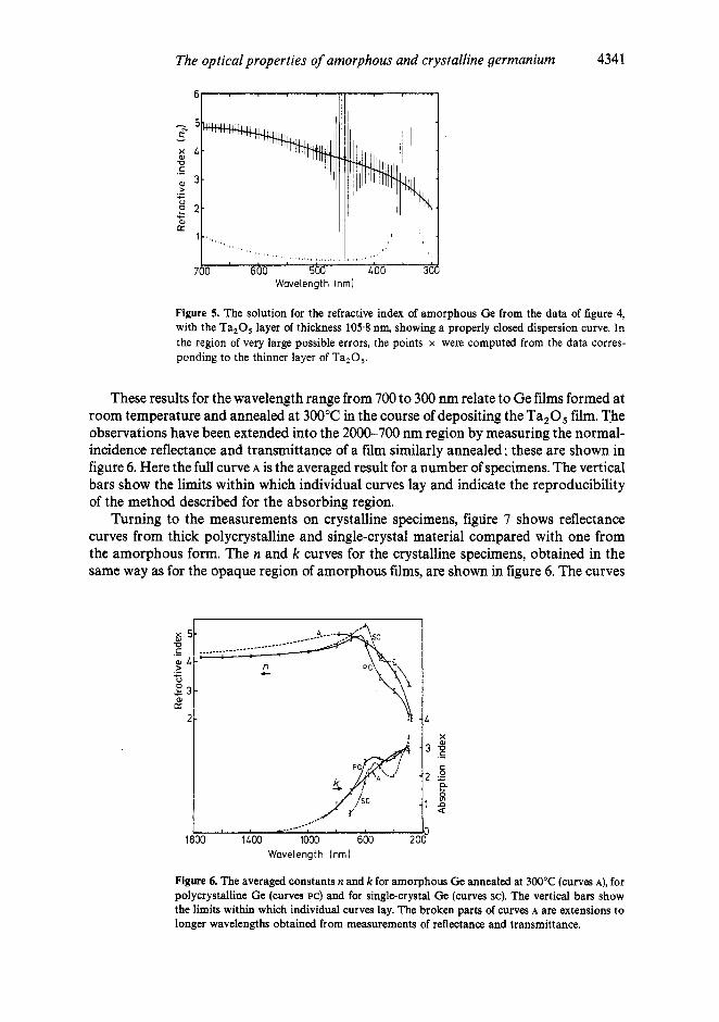
These results for the wavelength range from 700 to 300 nm relate to Ge films formed at room temperature and annealed at 300°C in the course of depositing the Ta,O, film. The observations have been extended into the 2000-700 nm region by measuring the normal- incidence reflectance and transmittance of a film similarly annealed ; these are shown in figure 6. Here the full curve A is the averaged result for a number of specimens. The vertical bars show the limits within which individual curves lay and indicate the reproducibility of the method described for the absorbing region.
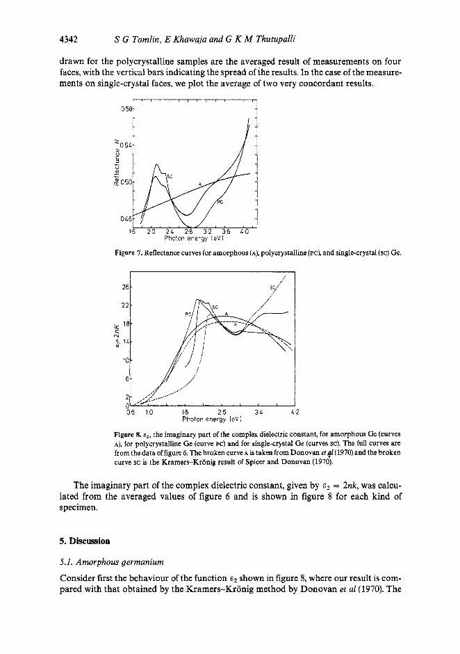
Turning to the measurements on crystalline specimens, figure 7 shows reflectance curves from thick polycrystalline and single-crystal material compared with one from the amorphous form. The n and k curves for the crystalline specimens, obtained in the same way as for the opaque region of amorphous films, are shown in figure 6. The curves
Wavelength Inml
Figure 6. The averaged constants n and k for amorphous Ge annealed at 300°C (curves A), for polycrystalline Ge (curves PC) and for single-crystal Ge (curves SC). The vertical bars show the limits within which individual curves lay. The broken parts of curves A are extensions to longer wavelengths obtained from measurements of reflectance and transmittance.
4342 S G Tomlin, E Khawaja and G K M Thutupalli
drawn for the polycrystalline samples are the averaged result of measurements on four faces, with the vertical bars indicating the spread of the results. In the case of the measure- ments on single-crystal faces, we plot the average of two very concordant results.
Figure 7. Reflectance curves for amorphous (A), polycrystalline (PC), and single-crystal (sc) Ge.
06 10 18 2 6 3 L L 2 Photon energy lev)
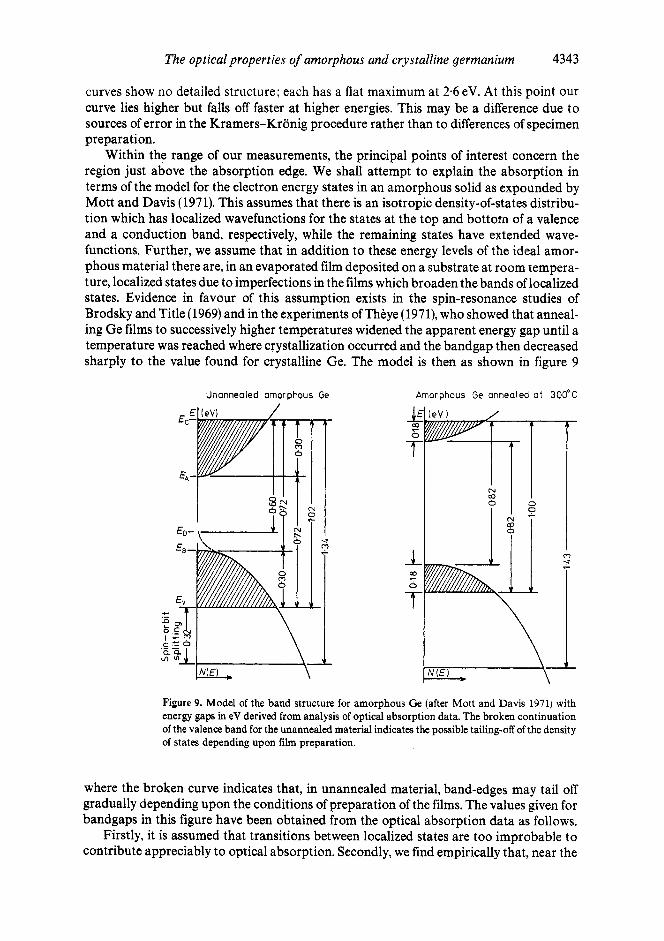
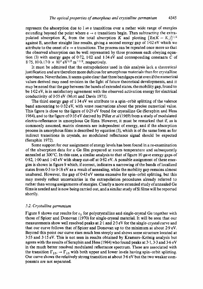
Figure 8. e l , the imaginary part of the complex dielectric constant, for amorphous Ge (curves A), for polycrystalline Ge (curve PC) and for single-crystal Ge (curves sc). The full curves are from the data of figure 6. The broken curve A is taken from Donovan et fl(1970) and the broken curve sc is the Kramers-Kronig result of Spicer and Donovan (1970).
The imaginary part of the complex dielectric constant, given by g2 = 2nk, was calcu- lated from the averaged values of figure 6 and is shown in figure 8 for each kind of specimen.
5. Discussion
5.1. Amorphous germanium
Consider first the behaviour of the function e2 shown in figure 8, where our result is com- pared with that obtained by the Kramers-Kronig method by Donovan et al(l970). The
The optical properties of amorphous and crystalline germanium 4343
curves show no detailed structure; each has a flat maximum at 2.6 eV. At this point our curve lies higher but falls off faster at higher energies. This may be a difference due to sources of error in the Kramers-Kronig procedure rather than to differences of specimen preparation.
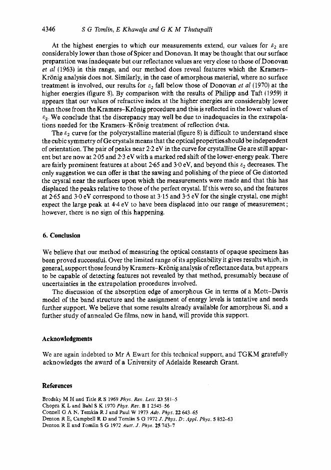
Within the range of our measurements, the principal points of interest concern the region just above the absorption edge. We shall attempt to explain the absorption in terms of the model for the electron energy states in an amorphous solid as expounded by Mott and Davis (1971). This assumes that there is an isotropic density-of-states distribu- tion which has localized wavefunctions for the states at the top and bottom of a valence and a conduction band, respectively, while the remaining states have extended wave- functions. Further, we assume that in addition to these energy levels of the ideal amor- phous material there are, in an evaporated film deposited on a substrate at room tempera- ture, localized states due to imperfections in the films which broaden the bands of localized states. Evidence in favour of this assumption exists in the spin-resonance studies of Brodsky and Title (1969) and in the experiments of Thbye (1971), who showed that anneal- ing Ge films to successively higher temperatures widened the apparent energy gap until a temperature was reached where crystallization occurred and the bandgap then decreased sharply to the value found for crystalline Ge. The model is then as shown in figure 9
Unannealed amorphous Ge Amorphous Ge annealed at 300°C
\ Figure 9. Model of the band structure for amorphous Ge (after Mott and Davis 1971) with energy gaps in eV derived from analysis of optical absorption data. The broken continuation of the valence band for the unannealed material indicates the possible tailing-off of the density of states depending upon film preparation.
where the broken curve indicates that, in unannealed material, band-edges may tail off gradually depending upon the conditions of preparation of the films. The values given for bandgaps in this figure have been obtained from the optical absorption data as follows.
Firstly, it is assumed that transitions between localized states are too improbable to contribute appreciably to optical absorption. Secondly, we find empirically that, near the
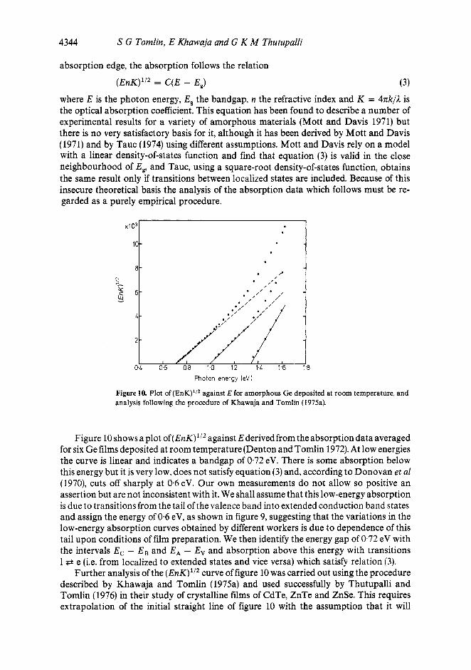
4344 S G Tomlin, E Khawaja and G K M Thutupalli
absorption edge, the absorption follows the relation
(EnK)”2 = C(E - E g ) (3) where E is the photon energy, E, the bandgap, n the refractive index and K = 4.nk/L is the optical absorption coefficient. This equation has been found to describe a number of experimental results for a variety of amorphous materials (Mott and Davis 1971) but there is no very satisfactory basis for it, although it has been derived by Mott and Davis (1971) and by Tauc (1974) using different assumptions. Mott and Davis rely on a model with a linear density-of-states function and find that equation (3) is valid in the close neighbourhood of E,, and Tauc, using a square-root density-of-states function, obtains the same result only if transitions between localized states are included. Because of this insecure theoretical basis the analysis of the absorption data which follows must be re- garded as a purely empirical procedure.
Photon energy (eV)
Figure 10. Plot of (EnK)’/2 against E for amorphous Ge deposited at room temperature, and analysis following the procedure of Khawaja and Tomlin (1975a).
Figure 10 shows a plot of(EnK)’I2 against Ederived from the absorption data averaged for six Ge films deposited at room temperature (Denton and Tomlin 1972). At low energies the curve is linear and indicates a bandgap of 0.72 eV. There is some absorption below this energy but it is very low, does not satisfy equation (3) and, according to Donovan et a1 (1970), cuts off sharply at 0.6 eV. Our own measurements do not allow so positive an assertion but are not inconsistent with it. We shall assume that this low-energy absorption is due to transitions from the tail of the valence band into extended conduction band states and assign the energy of 0-6 eV, as shown in figure 9, suggesting that the variations in the low-energy absorption curves obtained by different workers is due to dependence of this tail upon conditions of film preparation. We then identify the energy gap of 0.72 eV with the intervals E , - EB and E A - E, and absorption above this energy with transitions 1 P e (i.e. from localized to extended states and vice versa) which satisfy relation (3).
Further analysis of the (EnK)’” curve of figure 10 was carried out using the procedure described by Khawaja and Tomlin (1975a) and used successfully by Thutupalli and Tomlin (1976) in their study of crystalline films of CdTe, ZnTe and ZnSe. This requires extrapolation of the initial straight line of figure 10 with the assumption that it will
The optical properties of amorphous and crystalline germanium 4345
represent the absorption due to 1 e e transitions over a rather wide range of energies extending beyond the point where e + e transitions begin. Then subtracting the extra- polated absorption K , from the total absorption K and plotting [En(K - K , ) ] ' ' L against E, another straight line results, giving a second energy gap of 1.02 eV which we attribute to the onset of e -+ e transitions. The process can be repeated once more so that the observed absorption can be well represented by three processes each obeying equa- tion (3) with energy gaps of 0.72, 1.02 and l-34eV and corresponding constants C of 8.75, 10*0,17.0 x lo3 eV'I2 m-lI2 , respectively.
It must be admitted that the extrapolations used in this analysis lack a theoretical justification and are therefore more dubious for amorphous materials than for crystalline specimens. Nevertheless, it seems quite clear that three bandgaps exist even ifthe numerical values derived may need revision in the light of future theoretical developments, and it may be noted that the gap between the bands of extended states, the mobility gap, found to be 1.02 eV, is in satisfactory agreement with the observed activation energy for electrical conductivity of 0.55 eV (Mott and Davis 1971).
The third energy gap of 1-34 eV we attribute to a spin-orbit splitting of the valence band amounting to 0.32 eV, with some reservations about the precise numerical value. This figure is close to the figure of 0.29 eV found for crystalline Ge (Seraphin and Hess 1964), and to the figure of 0.35 eV derived by Piller et a1 (1969) from a study of modulated electro-reflectance in amorphous Ge films. However, it must be remarked that if, as is commonly assumed, matrix elements are independent of energy, and if the absorption process in amorphous films is described by equation (3), which is of the same form as for indirect transitions in crystals, no modulated reflectance signal should be expected (Seraphin 1972).
Some support for our assignment of energy levels has been found in a re-examination of the absorption data for a Ge film prepared at room temperature and subsequently annealed at 300°C. In this case, a similar analysis to that of figure 10 gave energy gaps of 0.82, 1.00 and 1.43 eV with sharp cut-off at 0.82 eV. A possible assignment of these ener- gies is shown in figure 9 which, if correct, indicates a narrowing of the bands of localized states from 0.3 to 0.18 eV as a result of annealing, while the mobility gap remains almost unaltered. However, the gap of 0.43 eV seems excessive for spin-orbit splitting, but this may merely reflect uncertainties in the extrapolation procedures already referred to rather than wrong assignments of energies. Clearly a more extended study of annealed Ge films is needed and is now being carried out, and a similar study of Si films will be reported shortly.
5.2. Crystalline germanium
Figure 8 shows our results for c2 for polycrystalline and single-crystal Ge together with those of Spicer and Donovan (1970) for single-crystal material. It will be seen that our measurements show well resolved peaks at 2.1 and 2.3 eV for the single-crystalcurve and that our curve follows that of Spicer and Donovan up to the minimum at about 2.9 eV. Beyond this point our curve rises much less steeply and shows some structure located at 3.55 and 3.15 eV. This is not seen in results obtained by Kramers-Kronig analysis but agrees with the results of Seraphin and Hess (1964) who found peaks at 3.1,3.3 and 3.6 eV in the much better resolved modulated reflectance spectrum. These are associated with the transition TZ5, -, rI5 with both upper and lower levels having spin-orbit splitting. Our curve shows the relatively strong transition at about 3.6 eV but the two weaker com- ponents are not separated.
4346 S G Tomlin, E Khawaja and G K M Thutupalli
At the highest energies to which our measurements extend, our values for e2 are considerably lower than those of Spicer and Donovan. It may be thought that our surface preparation was inadequate but our reflectance values are very close to those of Donovan et a1 (1963) in this range, and our method does reveal features which the Kramers- Kronig analysis does not. Similarly, in the case of amorphous material, where no surface treatment is involved, our results for E~ fall below those of Donovan et a1 (1970) at the higher energies (figure 8). By comparison with the results of Philipp and Taft (1959) it appears that our values of refractive index at the higher energies are considerably lower than those from the Kramers-Kronig procedure and this is reflected in the lower values of e2 . We conclude that the discrepancy may well be due to inadequacies in the extrapola- tions needed for the Kramers-Kronig treatment of reflection dsta.
The E~ curve for the polycrystalline material (figure 8) is difficult to understand since the cubic symmetry of Ge crystals means that the optical properties should be independent of orientation. The pair of peaks near 2.2 eV in the curve for crystalline Ge are still appar- ent but are now at 2-05 and 2.3 eV with a marked red shift of the lower-energy peak. There are fairly prominent features at about 2-65 and 3.0 eV, and beyond this .s2 decreases. The only suggestion we can offer is that the sawing and polishing of the piece of Ge distorted the crystal near the surfaces upon which the measurements were made and that this has displaced the peaks relative to those of the perfect crystal. If this were so, and the features at 2.65 and 3.0 eV correspond to those at 3-15 and 3.5 eV for the single crystal, one might expect the large peak at 4.4 eV to have been displaced into our range of measurement ; however, there is no sign of this happening.
6. Conclusion
We believe that our method of measuring the optical constants of opaque specimens has been proved successful. Over the limited range of its applicability it gives results which, in general, support those found by Kramers-Kronig analysis of reflectance data, but appears to be capable of detecting features not revealed by that method, presumably because of uncertainties in the extrapolation procedures involved.
The discussion of the absorption edge of amorphous Ge in terms of a Mott-Davis model of the band structure and the assignment of energy levels is tentative and needs further support. We believe that some results already available for amorphous Si, and a further study of annealed Ge films, now in hand, will provide this support.
Acknowledgments
We are again indebted to Mr A Ewart for this technical support, and TGKM gratefully acknowledges the award of a University of Adelaide Research Grant.
References
Brodsky M H and Title R S 1969 Phys. Rev. Letr. 23 581-5 Chopra K L and Bahl S K 1970 Phys. Rev. B 1 2545--56 Connell G A N, Temkin R J and Paul W 1973 Adv. Phys. 22 643-65 Denton R E, Campbell R D and Tomlin S G 1972 J . Phys. D : Appl. Phys. 5 852--63 Denton R E and Tomlin S G 1972 Aust. J . Phys. 25 743-7
The optical properties of amorphous and crystalline germanium 4347
Donovan T M, Ashley E J and Bennett H E 1963 J . O p f . Soc. Am. 53 1403-9 Donovan T M, Spicer W E, Bennett J M and Ashley E J 1970 Phys. Rev. B 2 397-413 Khawaja E E 1975 Thesis University of Adelaide Khawaja E E and Tomlin S G 1975a J . Phys. D : Appl. Phys. 8 581-94 - Mott N F and Davis E A 1971 Elecfronic Processes in Non-crystalline Solids (Oxford: Clarendon Press) Paul W, Connell G A N and Temkin R J 1973 Adv. Phys. 22 531-80 Phillipp H R and Taft E A 1959 Phys. Rev. 113 1002--5 Piller H, Seraphin B 0, Markel K and Fischer J E 1969 Phys. Rev. Lef t . 23 775-8 Seraphin B 0 1972 Optical Properfies of Solids ed F Abelhs (Amsterdam: North-Holland) pp 163--276 Seraphin B 0 and Bennett H E 1967 Semiconductors and Semimetals Vol3 eds R K Willardson and A C Beer
Seraphin B 0 and Hess R B 1964 Phys. Rev. Lef t . 14 138-40 Spicer W E and Donovan T M 1970 J . Non-Cryst. Solids 2 6680 Tauc J 1974 Amorphour and Liquid Semiconductors ed J Tauc (London and New York : Plenum Press) pp 159--
Tauc J and Abraham A 1969 Czech. J . Phys. B 19 1246-54 Theye M L 1971 Mater. Res. Bull. 6 103-18 Thutupalli G K M and Tomlin S G 1976 J . Phys. D : Appl. Phys. 9 1639-46 Tomlin S G 1972 Thin Solid Films 13 265-8 Vincent-Geisse J 1964 J . Physique 25 291-4 Vincent-Geisse J, Ngugen Tan Tai and Pinan-Eucarre J P 1967 J. Physique 28 26-30
1975b Thin Solid Films 30 361-9
(New York: Academic Press) pp 449--543
220