Embed Size (px)
Citation preview
Subscriber access provided by BOSTON COLLEGE
Nano Letters is published by the American Chemical Society. 1155 SixteenthStreet N.W., Washington, DC 20036
Letter
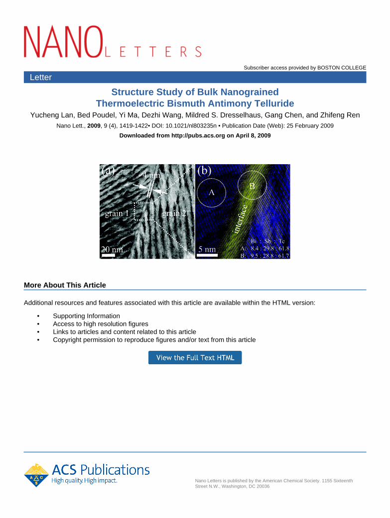
Structure Study of Bulk NanograinedThermoelectric Bismuth Antimony Telluride
Yucheng Lan, Bed Poudel, Yi Ma, Dezhi Wang, Mildred S. Dresselhaus, Gang Chen, and Zhifeng RenNano Lett., 2009, 9 (4), 1419-1422• DOI: 10.1021/nl803235n • Publication Date (Web): 25 February 2009
Downloaded from http://pubs.acs.org on April 8, 2009
More About This Article
Additional resources and features associated with this article are available within the HTML version:
• Supporting Information• Access to high resolution figures• Links to articles and content related to this article• Copyright permission to reproduce figures and/or text from this article
Structure Study of Bulk NanograinedThermoelectric Bismuth AntimonyTellurideYucheng Lan,† Bed Poudel,‡ Yi Ma,†,‡ Dezhi Wang,† Mildred S. Dresselhaus,§Gang Chen,*,| and Zhifeng Ren*,†
Department of Physics, Boston College, Chestnut Hill, Massachusetts 02467, GMZEnergy, Inc., 12A Hawthorn Street, Newton, Massachusetts 02458, and Department ofPhysics, Department of Electrical Engineering and Computer Science, Department ofMechanical Engineering, Massachusetts Institute of Technology,Cambridge, Massachusetts 02139
Received October 26, 2008; Revised Manuscript Received January 2, 2009
ABSTRACT
The microstructures of bulk nanograined p-type bismuth antimony telluride with a thermoelectric dimensionless figure-of-merit ZT ) 1.4 areinvestigated using transmission electron microscopy. It is found that the bulk material contains both nano- and microsized grains. Betweenthe nanograins, bismuth-rich interface regions with a 4 nm thickness were detected. In addition, nanoprecipitates as well as other defects arealso found to be embedded in the nanograins. The high ZT is attributed to the slight increase in the electrical conductivity, and to the largedecrease of the thermal conductivity.
Since the 1950s, thermoelectric materials that convertelectrical energy into thermal energy or vice versa have beenused in cooling, refrigeration, and power generation.1–3 Theeffectiveness of a thermoelectric material is related to itsdimensionless thermoelectric figure-of-merit ZT ) (S2σ/k)T,where S, σ, k, and T are the Seebeck coefficient, electricalconductivity, thermal conductivity, and absolute temperature,respectively.1 Up to now, reasonably high ZT values havebeen achieved in either single crystalline bulk ingots4,5 orsuperlattices6–8 and nanostructured bulk materials.9–11 Thesignificant enhancement of ZT from 1 in the commercialingot to 1.4 in the nanograined bulk bismuth antimonytelluride (BixSb2-xTe3) alloy,10,11 as the result of the reductionin thermal conductivity and the increase in electricalconductivity, is closely related to the unique microstructuresof the nanograined bulk material. This work reports a detailedstudy of microstructures and elemental microanalysis of suchnanograined bulk materials. Throughout the paper, only aqualitative correlation between the microstructure and ther-moelectric properties is presented. A quantitative analysisis much more difficult at this stage. The structural information
obtained from these investigations will contribute in a majorway to guiding modeling of the scattering processes deter-mining the calculation of the thermal conductivity ofnanograined BiSbTe composite materials with an eye towardfurther improvement of the materials processing of thenanocomposites and leading to further increases in ZT.
Experimental Section. The nanograined bulk BixSb2-xTe3
was prepared by a ball milling and hot-press method.10,11
TEM specimens were prepared from the nanograined bulkBixSb2-xTe3 by dicing, mechanical polishing, and Ar+-ionmilling. The microstructures were investigated using a JEOL-2010F transmission electron microscope (TEM) operated at200 kV. The microstructures of the crystalline ingot werealso studied for comparison. For the statistics of grain andprecipitate size, only those particles neighboring more thantwo other particles are counted as grains. All other particlesembedded in grains or located between two grains areconsidered as precipitates. The area of each grain orprecipitate was measured and converted into a maximumcross-sectional area of an equivalent sphere.
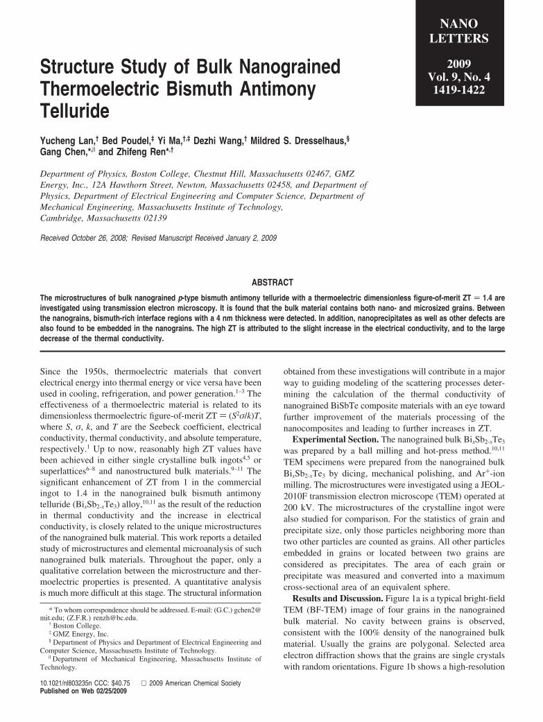
Results and Discussion. Figure 1a is a typical bright-fieldTEM (BF-TEM) image of four grains in the nanograinedbulk material. No cavity between grains is observed,consistent with the 100% density of the nanograined bulkmaterial. Usually the grains are polygonal. Selected areaelectron diffraction shows that the grains are single crystalswith random orientations. Figure 1b shows a high-resolution
* To whom correspondence should be addressed. E-mail: (G.C.) [email protected]; (Z.F.R.) [email protected].
† Boston College.‡ GMZ Energy, Inc.§ Department of Physics and Department of Electrical Engineering and
Computer Science, Massachusetts Institute of Technology.| Department of Mechanical Engineering, Massachusetts Institute of
Technology.
NANOLETTERS
2009Vol. 9, No. 41419-1422
10.1021/nl803235n CCC: $40.75 2009 American Chemical SocietyPublished on Web 02/25/2009
TEM (HRTEM) image of grain boundaries between threeadjacent grains. The high-angle grain boundaries are wellcrystallized and free of second phase material. The random-ness of the crystalline orientation of the adjacent grainspromotes phonon scattering significantly. Figure 1c showsan HRTEM image of smaller grains. These small grains arealso single crystals and are closely packed, similar to thebigger grains shown in Figure 1a.
Figure 1d shows the grain size distribution. Clearly, themajority of the grains are of diameters below 1.6 µm. Theinset of Figure 1d shows that 12% of the grains have adiameter less than 20 nm and 5% have a diameter in the20-40 nm range. The grain boundaries scatter phonons withmean free paths comparable to the grain size, therebyreducing the thermal conductivity. The wide grain sizedistribution shown in Figure 1d is responsible for scatteringphonons with a variety of wavelengths. Small particlesembedded in larger particles also provide effective phononscattering centers, as discussed below.
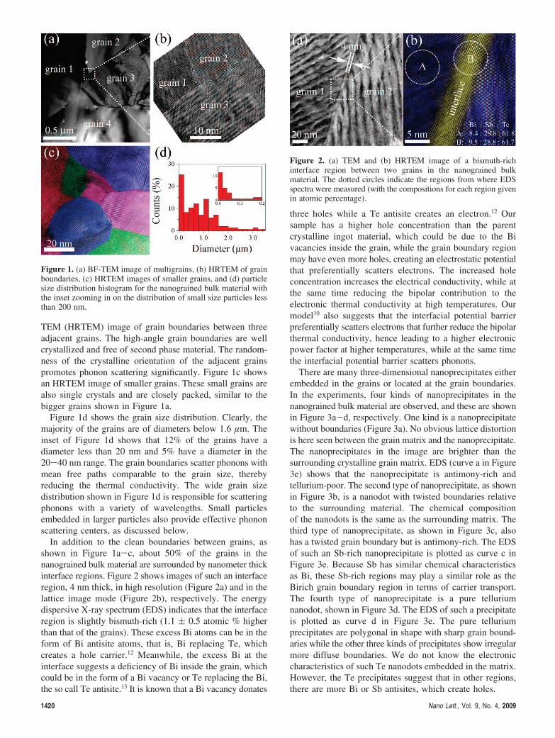
In addition to the clean boundaries between grains, asshown in Figure 1a-c, about 50% of the grains in thenanograined bulk material are surrounded by nanometer thickinterface regions. Figure 2 shows images of such an interfaceregion, 4 nm thick, in high resolution (Figure 2a) and in thelattice image mode (Figure 2b), respectively. The energydispersive X-ray spectrum (EDS) indicates that the interfaceregion is slightly bismuth-rich (1.1 ( 0.5 atomic % higherthan that of the grains). These excess Bi atoms can be in theform of Bi antisite atoms, that is, Bi replacing Te, whichcreates a hole carrier.12 Meanwhile, the excess Bi at theinterface suggests a deficiency of Bi inside the grain, whichcould be in the form of a Bi vacancy or Te replacing the Bi,the so call Te antisite.13 It is known that a Bi vacancy donates
three holes while a Te antisite creates an electron.12 Oursample has a higher hole concentration than the parentcrystalline ingot material, which could be due to the Bivacancies inside the grain, while the grain boundary regionmay have even more holes, creating an electrostatic potentialthat preferentially scatters electrons. The increased holeconcentration increases the electrical conductivity, while atthe same time reducing the bipolar contribution to theelectronic thermal conductivity at high temperatures. Ourmodel10 also suggests that the interfacial potential barrierpreferentially scatters electrons that further reduce the bipolarthermal conductivity, hence leading to a higher electronicpower factor at higher temperatures, while at the same timethe interfacial potential barrier scatters phonons.
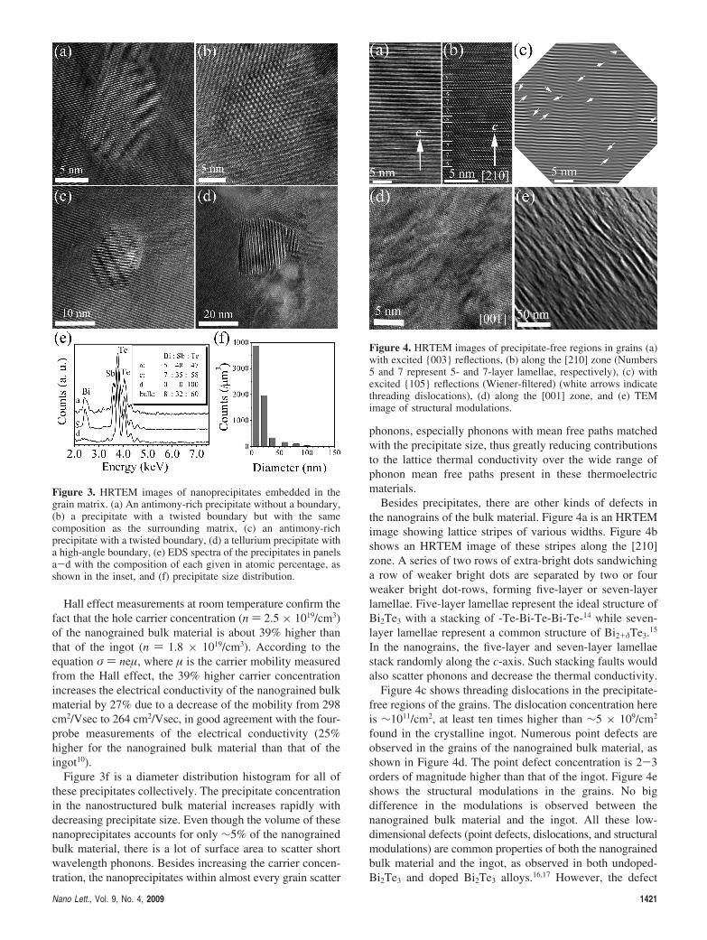
There are many three-dimensional nanoprecipitates eitherembedded in the grains or located at the grain boundaries.In the experiments, four kinds of nanoprecipitates in thenanograined bulk material are observed, and these are shownin Figure 3a-d, respectively. One kind is a nanoprecipitatewithout boundaries (Figure 3a). No obvious lattice distortionis here seen between the grain matrix and the nanoprecipitate.The nanoprecipitates in the image are brighter than thesurrounding crystalline grain matrix. EDS (curve a in Figure3e) shows that the nanoprecipitate is antimony-rich andtellurium-poor. The second type of nanoprecipitate, as shownin Figure 3b, is a nanodot with twisted boundaries relativeto the surrounding material. The chemical compositionof the nanodots is the same as the surrounding matrix. Thethird type of nanoprecipitate, as shown in Figure 3c, alsohas a twisted grain boundary but is antimony-rich. The EDSof such an Sb-rich nanoprecipitate is plotted as curve c inFigure 3e. Because Sb has similar chemical characteristicsas Bi, these Sb-rich regions may play a similar role as theBirich grain boundary region in terms of carrier transport.The fourth type of nanoprecipitate is a pure telluriumnanodot, shown in Figure 3d. The EDS of such a precipitateis plotted as curve d in Figure 3e. The pure telluriumprecipitates are polygonal in shape with sharp grain bound-aries while the other three kinds of precipitates show irregularmore diffuse boundaries. We do not know the electroniccharacteristics of such Te nanodots embedded in the matrix.However, the Te precipitates suggest that in other regions,there are more Bi or Sb antisites, which create holes.
Figure 1. (a) BF-TEM image of multigrains, (b) HRTEM of grainboundaries, (c) HRTEM images of smaller grains, and (d) particlesize distribution histogram for the nanograined bulk material withthe inset zooming in on the distribution of small size particles lessthan 200 nm.
Figure 2. (a) TEM and (b) HRTEM image of a bismuth-richinterface region between two grains in the nanograined bulkmaterial. The dotted circles indicate the regions from where EDSspectra were measured (with the compositions for each region givenin atomic percentage).
1420 Nano Lett., Vol. 9, No. 4, 2009
Hall effect measurements at room temperature confirm thefact that the hole carrier concentration (n ) 2.5 × 10¹⁹/cm3)of the nanograined bulk material is about 39% higher thanthat of the ingot (n ) 1.8 × 10¹⁹/cm3). According to theequation σ ) neµ, where µ is the carrier mobility measuredfrom the Hall effect, the 39% higher carrier concentrationincreases the electrical conductivity of the nanograined bulkmaterial by 27% due to a decrease of the mobility from 298cm2/Vsec to 264 cm2/Vsec, in good agreement with the four-probe measurements of the electrical conductivity (25%higher for the nanograined bulk material than that of theingot10).
Figure 3f is a diameter distribution histogram for all ofthese precipitates collectively. The precipitate concentrationin the nanostructured bulk material increases rapidly withdecreasing precipitate size. Even though the volume of thesenanoprecipitates accounts for only ∼5% of the nanograinedbulk material, there is a lot of surface area to scatter shortwavelength phonons. Besides increasing the carrier concen-tration, the nanoprecipitates within almost every grain scatter
phonons, especially phonons with mean free paths matchedwith the precipitate size, thus greatly reducing contributionsto the lattice thermal conductivity over the wide range ofphonon mean free paths present in these thermoelectricmaterials.
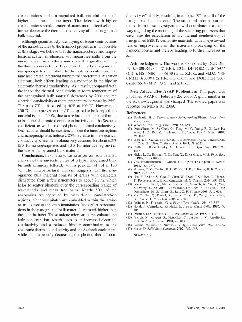
Besides precipitates, there are other kinds of defects inthe nanograins of the bulk material. Figure 4a is an HRTEMimage showing lattice stripes of various widths. Figure 4bshows an HRTEM image of these stripes along the [210]zone. A series of two rows of extra-bright dots sandwichinga row of weaker bright dots are separated by two or fourweaker bright dot-rows, forming five-layer or seven-layerlamellae. Five-layer lamellae represent the ideal structure ofBi2Te3 with a stacking of -Te-Bi-Te-Bi-Te-14 while seven-layer lamellae represent a common structure of Bi2+δTe3.15
In the nanograins, the five-layer and seven-layer lamellaestack randomly along the c-axis. Such stacking faults wouldalso scatter phonons and decrease the thermal conductivity.
Figure 4c shows threading dislocations in the precipitate-free regions of the grains. The dislocation concentration hereis ∼1011/cm2, at least ten times higher than ∼5 × 10⁹/cm2
found in the crystalline ingot. Numerous point defects areobserved in the grains of the nanograined bulk material, asshown in Figure 4d. The point defect concentration is 2-3orders of magnitude higher than that of the ingot. Figure 4eshows the structural modulations in the grains. No bigdifference in the modulations is observed between thenanograined bulk material and the ingot. All these low-dimensional defects (point defects, dislocations, and structuralmodulations) are common properties of both the nanograinedbulk material and the ingot, as observed in both undoped-Bi2Te3 and doped Bi2Te3 alloys.16,17 However, the defect
Figure 3. HRTEM images of nanoprecipitates embedded in thegrain matrix. (a) An antimony-rich precipitate without a boundary,(b) a precipitate with a twisted boundary but with the samecomposition as the surrounding matrix, (c) an antimony-richprecipitate with a twisted boundary, (d) a tellurium precipitate witha high-angle boundary, (e) EDS spectra of the precipitates in panelsa-d with the composition of each given in atomic percentage, asshown in the inset, and (f) precipitate size distribution.
Figure 4. HRTEM images of precipitate-free regions in grains (a)with excited {003} reflections, (b) along the [210] zone (Numbers5 and 7 represent 5- and 7-layer lamellae, respectively), (c) withexcited {105} reflections (Wiener-filtered) (white arrows indicatethreading dislocations), (d) along the [001] zone, and (e) TEMimage of structural modulations.
Nano Lett., Vol. 9, No. 4, 2009 1421
concentrations in the nanograined bulk material are muchhigher than those in the ingot. The defects with higherconcentrations would scatter phonons more effectively andfurther decrease the thermal conductivity of the nanograinedbulk material.
Although quantitatively identifying different contributionsof the nanostructures to the transport properties is not possibleat this stage, we believe that the nanostructures and imper-fections scatter all phonons with mean free paths from themicron scale down to the atomic scale, thus greatly reducingthe thermal conductivity. Bismuth-rich interface regions andnanoprecipitates contribute to the hole concentration, andmay also create interfacial barriers that preferentially scatterelectrons, both effects leading to a reduction in the bipolarelectronic thermal conductivity. As a result, compared withthe ingot, the thermal conductivity at room temperature ofthe nanograined bulk material decreases by 20% and theelectrical conductivity at room temperature increases by 25%.The peak ZT is increased by 40% at 100 °C. However, at250 °C the improvement in ZT compared to bulk crystallinematerial is about 200%, due to a reduced bipolar contributionto both the electronic thermal conductivity and the Seebeckcoefficient, as well as reduced phonon thermal conductivity.One fact that should be mentioned is that the interface regionsand nanoprecipitates induce a 25% increase in the electricalconductivity while their volume only accounts for about 6.3%(5% for nanoprecipitates and 1.3% for interface regions) ofthe whole nanograined bulk material.
Conclusions. In summary, we have performed a detailedanalysis of the microstructures of p-type nanograined bulkbismuth antimony telluride with a peak ZT of 1.4 at 100°C. The microstructural analysis suggests that the nan-ograined bulk material consists of grains with diametersdistributed from a few nanometers to about 2 µm, whichhelps to scatter phonons over the corresponding reange ofwavelengths and mean free paths. Nearly 50% of thenanograins are separated by bismuth-rich nanointerfaceregions. Nanoprecipitates are embedded within the grainsor are located at the grain boundaries. The defect concentra-tions in the nanograined bulk material are much higher thanthose of the ingot. These unique microstructures enhance thehole concentration, which leads to an increased electricalconductivity and a reduced bipolar contribution to theelectronic thermal conductivity and the Seebeck coefficient,while simultaneously decreasing the phonon thermal con-
ductivity efficiently, resulting in a higher ZT overall of thenanograined bulk material. The structural information ob-tained from these investigations will contribute in a majorway to guiding the modeling of the scattering processes thatenter into the calculation of the thermal conductivity ofnanograined BiSbTe composite materials, with an eye towardfurther improvement of the materials processing of thenanocomposites and thereby leading to further increases inZT.
Acknowledgment. The work is sponsored by DOE DE-FG02-00ER45805 (Z.F.R.), DOE DE-FG02-02ER45977(G.C.), NSF NIRT 0506830 (G.C., Z.F.R., and M.D.), NSFCMMI 0833084 (Z.F.R. and G.C.), and DOE DE-FG02-08ER46516 (M.D., G.C., and Z.F.R.).
Note Added after ASAP Publication: This paper waspublished ASAP on February 25, 2009. A grant number inthe Acknowledgment was changed. The revised paper wasreposted on March 10, 2009.
References(1) Goldsmid, H. J. Thermoelectric Refrigeration; Plenum Press, New
York, 1964.(2) Wood, C. Rep. Prog. Phys. 1988, 51, 459.(3) Dresselhaus, M. S.; Chen, G.; Tang, M. Y.; Yang, R. G.; Lee, H.;
Wang, D. Z.; Ren, Z. F.; Fleurial, J. P.; Gogna, P. AdV. Mater. 2007,19, 1043.
(4) Morelli, T.; Caillat, T.; Fleurial, J. P.; Borshchevsky, A.; Vandersande,J.; Chen, B.; Uher, C. Phys. ReV. B 1995, 51, 9622.
(5) Caillat, T.; Borshchevsky, A.; Fleurial, J. P. J. Appl. Phys. 1996, 80,4442.
(6) Hicks, L. D.; Harman, T. C.; Sun, X.; Dresselhaus, M. S. Phys. ReV.B 1996, 53, R10493.
(7) Venkatasubramanian, R.; Siivola, E.; Colpitts, T.; O’Quinn, B. Nature2001, 413, 597.
(8) Harman, T. C.; Taylor, P. J.; Walsh, M. P.; LaForge, B. E. Science2002, 297, 2229.
(9) Hsu, K. F.; Loo, S.; Guo, F.; Chen, W.; Dyck, J. S.; Uher, C.; Hogan,T.; Polychroniadis, E. K.; Kanatzidis, M. G. Science 2004, 303, 818.
(10) Poudel, B.; Hao, Q.; Ma, Y.; Lan, Y. C.; Minnich, A.; Yu, B.; Yan,X.; Wang, D. Z.; Muto, A.; Vashaee, D.; Chen, X. Y.; Liu, J. M.;Dresselhaus, M. S.; Chen, G.; Ren, Z. F. Science 2008, 320, 634.
(11) Ma, Y.; Hao, Q.; Poudel, B.; Lan, Y. C.; Yu, B.; Wang, D. Z.; Chen,G.; Ren, Z. F. Nano Lett. 2008, 8, 2580.
(12) Pecheur, P.; Toussaint, G. J. Phys. Chem. Solids 1994, 35, 327.(13) Horak, J.; Cermak, K.; Koudelka, L. J. Phys. Chem. Solids 1986, 47,
805.(14) Drabble, J.; Goodman, C. J. Phys. Chem. Solids 1958, 5, 142.(15) Frangis, N.; Kuypers, S.; Manolikas, C.; Landuyt, J. V.; Amelinckx,
S. Solid State Commun. 1989, 69, 817.(16) Peranio, N.; Eibl, O.; Nurnus, J. J. Appl. Phys. 2006, 100, 114306.(17) Maier, D. Solid State Commun. 2002, 122, 565.
NL803235N
1422 Nano Lett., Vol. 9, No. 4, 2009


![Photonic crystal fibres: mapping Maxwell’s equations onto a ... · silicate glass [4], telluride glass [5], bismuth glass [6], silver halide [7], teflon [8], and plastics/polymers](https://img.pdfslide.net/doc/110x75/606f995dd7e2a6344347eb2f/photonic-crystal-ibres-mapping-maxwellas-equations-onto-a-silicate-glass.jpg)