Embed Size (px)
Citation preview
Three-Phase Multi-Level DC-AC Converter Using Three-Phase Coupled Inductors
Ivo Barbi1 and Romeu Hausmann2 1Federal University of Santa Catarina – UFSC, Power Electronics Institute – INEP
Florianopolis – SC- Brazil, [email protected] 2Department of Electrical and Telecommunication Engineering, University of Blumenau – FURB
Blumenau – SC – Brazil, [email protected]
Abstract – A new three-phase multi-level DC-AC
converter with three-phase coupled inductors is presented in this work. The related converter is employed only as an inverter here. Initially the power stage diagram and the modulator are shown and discussed. Their main characteristics are described and the more relevant waveforms, generated by simulation, are shown. Next, the operation of the converter with sinusoidal PWM modulation is discussed and some relevant figures are presented. The vectorial interpretation of the line load voltage is shown to all available vectors of load voltage in the new structure. Finally, experimental results obtained from the implemented prototype are presented and briefly discussed.
Keywords - Coupled inductor; DC-AC bidirectional
converter; three-phase inverter.
I. INTRODUCTION The search for alternatives to the reduction of inverters
output filters volume is presented in some publications in Power Electronics. The motivation is that the raised volume of the filter reflects directly in the cost of the filters and the amount of circulating reactive energy in the converter.
Several techniques are used to increase the amount of energy processed from static converters, amongst which the interleaving technique, multilevel converters and the use of cells of inductive coupling.
The interleaving technique is widely treated in the literature and consists of connecting converters in parallel, with synchronized and complementary operation, connected to the same load and with the same power source. Interleaved converters can be classified in two ways: without magnetic coupling and with magnetic coupling.
In [1] the analysis of an interleaved boost converter with coupled inductors is presented. The related work considers a sensorless balance currents method. The technique consists of operating the two boost converters in discontinuous conduction mode, in such a way that the total input current of the converters is continuous and can be considered constant.
In [2] is presented a generic model for interleaved multiphase boost converter, with coupled inductors. The mathematical development is presented considering “2N” boost converters, and the number of converters is always multiple of 2.
The use of coupled inductors to improve the current capacity in inverters is presented in [3]. In this structure, techniques are proposed for paralleling the inverters, always
in pairs. Beyond reducing the current stresses in the power devices, the structure also provides the reduction of the harmonic content in the output voltage. The proposal topology can be applied in three-phase inverters and be generalized for a bigger number of converters in parallel, with the disadvantage of only allowing converters in pairs.
The use of multilevel coupled inductors in single-phase boost rectifiers is presented in [4]. This work presents a comparison between the inductors in converters using interleaving and multilevel coupled inductors. Structures with 3, 4 and 5 levels are shown, and the structure with 4 levels are emphasized because it is possible the use of a commercial three-phase core.
Another solution for high power static converters is the use of multilevel converters. As characteristic, these converters present reduction of the voltage stresses on the switches and have output multilevel voltage. This can be obtained through three techniques: the series and/or parallel association of the switches, the use of multilevel commutation cell and the converters association [5], [6] and [7].
The concept of three-state commutation cells is presented in [9], and it is based on the two-state switching cell shown in [8]. The main characteristics of the three-state cell are the division of the current who flows through the switches and the frequency multiplication of the load voltage. These characteristics allow improvement of the losses distribution and the volume reduction of the output filter. The four-state switching cell is shown in [10] and [11] and consists of three switches, three diodes and a three-phase Y connected transformer. In this structure the frequency at the output filter is triple the switching frequency and the switches current is balanced divided and equal to 1/3 of the output current.
The switching cell is formed with the substitution of the 2 states cell, shown in [8], for a 3, 4 or “n” states cell, maintaining the other elements of the converter.
II. STRUCTURE PRESENTATION The three-phase DC-AC converter with coupled inductor
is presented in Fig. 1. The use of the three-phase coupled inductor allows the division of the load phase current through the switches, in a balanced way so that the current in each arm of the structure is equal to 1/3 of the load current in one phase, reducing the current values for the switches. Another characteristic of this structure is the increasing of the voltage load levels, thus contributing to reduce the common mode voltage, when compared with standard structures. The load
978-1-4244-3370-4/09/$25.00 © 2009 IEEE 332
voltage frequency is three times the switch frequency; this results in a reduction of the size and the cost of the output filter.
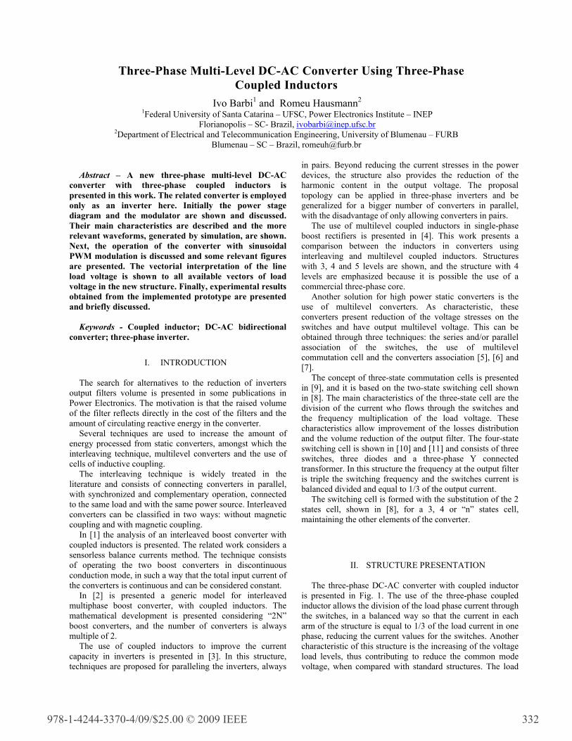
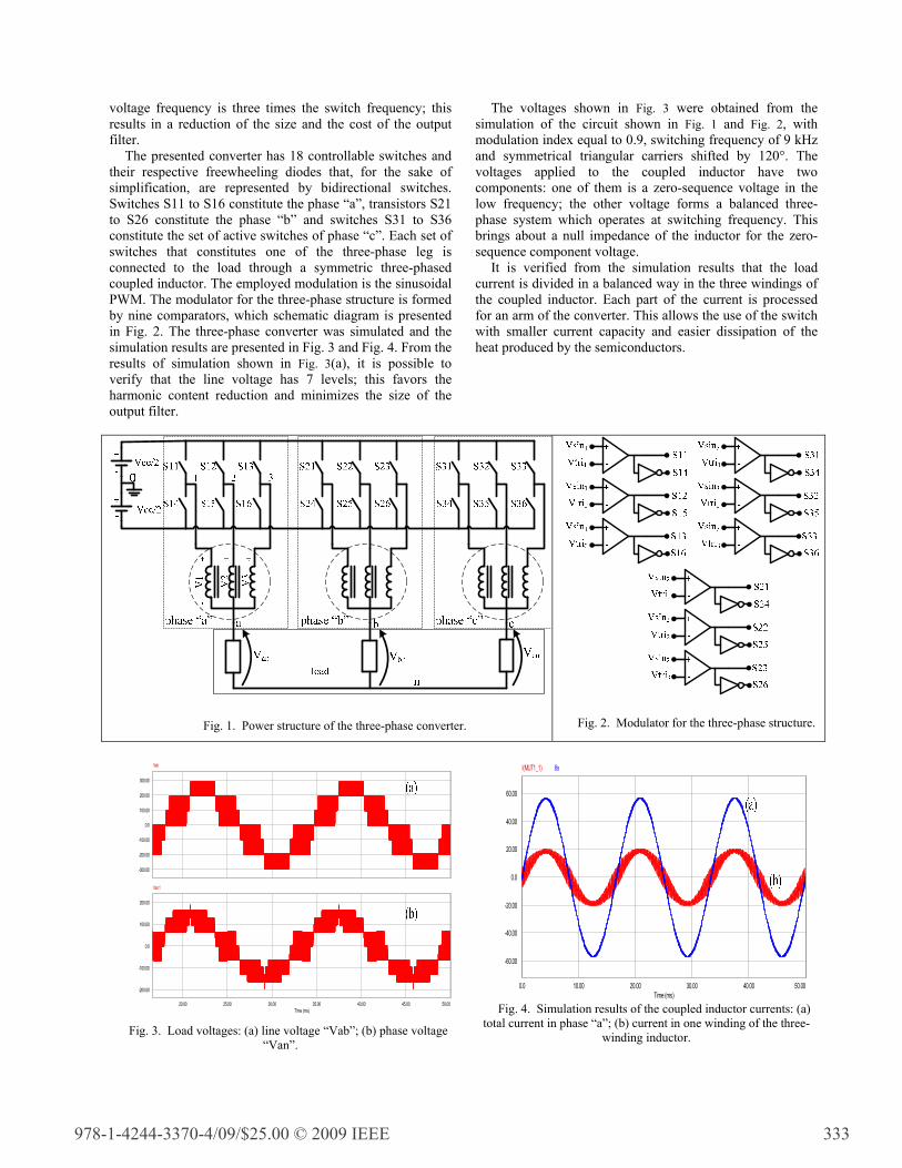
The presented converter has 18 controllable switches and their respective freewheeling diodes that, for the sake of simplification, are represented by bidirectional switches. Switches S11 to S16 constitute the phase “a”, transistors S21 to S26 constitute the phase “b” and switches S31 to S36 constitute the set of active switches of phase “c”. Each set of switches that constitutes one of the three-phase leg is connected to the load through a symmetric three-phased coupled inductor. The employed modulation is the sinusoidal PWM. The modulator for the three-phase structure is formed by nine comparators, which schematic diagram is presented in Fig. 2. The three-phase converter was simulated and the simulation results are presented in Fig. 3 and Fig. 4. From the results of simulation shown in Fig. 3(a), it is possible to verify that the line voltage has 7 levels; this favors the harmonic content reduction and minimizes the size of the output filter.
The voltages shown in Fig. 3 were obtained from the simulation of the circuit shown in Fig. 1 and Fig. 2, with modulation index equal to 0.9, switching frequency of 9 kHz and symmetrical triangular carriers shifted by 120°. The voltages applied to the coupled inductor have two components: one of them is a zero-sequence voltage in the low frequency; the other voltage forms a balanced three-phase system which operates at switching frequency. This brings about a null impedance of the inductor for the zero-sequence component voltage.
It is verified from the simulation results that the load current is divided in a balanced way in the three windings of the coupled inductor. Each part of the current is processed for an arm of the converter. This allows the use of the switch with smaller current capacity and easier dissipation of the heat produced by the semiconductors.
Fig. 1. Power structure of the three-phase converter.
Fig. 2. Modulator for the three-phase structure.
0.0
-100.00
-200.00
-300.00
100.00
200.00
300.00
Vab
20.00 25.00 30.00 35.00 40.00 45.00 50.00Time (ms)
0.0
-100.00
-200.00
100.00
200.00
Van1
Fig. 3. Load voltages: (a) line voltage “Vab”; (b) phase voltage
“Van”.
0.0 10.00 20.00 30.00 40.00 50.00Time (ms)
0.0
-20.00
-40.00
-60.00
20.00
40.00
60.00
I(MUT1_1) Ifa
Fig. 4. Simulation results of the coupled inductor currents: (a)
total current in phase “a”; (b) current in one winding of the three-winding inductor.
978-1-4244-3370-4/09/$25.00 © 2009 IEEE 333
III. CONVERTER OPERATION Considering the structure presented, in Fig. 6
representative waveforms are shown to evidence two important characteristics of this structure. The first one is that the Va0 voltage has a three times higher frequency compared with the switching frequency; this allows the reduction of the size of the output filter. The other important characteristic is that the V10 voltage has two levels and the Va0 has four levels of voltage; thus a change of 2 to 4 levels in the output voltage.
+
-
v2
+
-
v1
+
-
v3
+
-
Vcc/2
+
- Vcc/2
a0+
-
v1
+
-
v2
+
-
v3
+
-
Vcc/2
+
- Vcc/2
a0+
-
v1
+
-
v3
+
-
v2
+
-
Vcc/2
+
- Vcc/2
a0
+
-
v2
+
-
v1
+
-
v3+
-
Vcc/2
+
- Vcc/2
a0
+
-
v1
+
-
v3
+
-
v2+
-
Vcc/2
+
- Vcc/2
a0
+
-
v1
+
-
v2
+
-
v3+
-
Vcc/2
+
- Vcc/2
a0
+
-
v1
+
-
v2
+
-
v3+
-
Vcc/2
+
- Vcc/2
a0+
-
v1
+
-
v2
+
-
v3
+
-
Vcc/2
+
- Vcc/2
a0
(1) (2) (3)
(4) (5) (6)
(7) (8) Fig. 5. Topological possible states for one phase of the
converter.
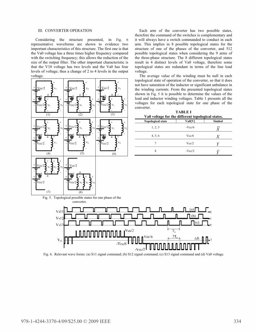
Each arm of the converter has two possible states, therefore the command of the switches is complementary and it will always have a switch commanded to conduct in each arm. This implies in 8 possible topological states for the structure of one of the phases of the converter, and 512 possible topological states when considering the 9 arms of the three-phase structure. The 8 different topological states result in 4 distinct levels of Va0 voltage, therefore some topological states are redundant in terms of the line load voltage.
The average value of the winding must be null in each topological state of operation of the converter, so that it does not have saturation of the inductor or significant unbalance in the winding currents. From the presented topological states shown in Fig. 5 it is possible to determine the values of the load and inductor winding voltages. Table 1 presents all the voltages for each topological state for one phase of the converter.
TABLE I Va0 voltage for the different topological states. Topological state Va0[V] Simbol
1, 2, 3 -Vcc/6 X4, 5, 6 Vcc/6 X
7 Vcc/2 Y8 -Vcc/2 Y
Fig. 6. Relevant wave forms: (a) S11 signal command; (b) S12 signal command; (c) S13 signal command and (d) Va0 voltage.
978-1-4244-3370-4/09/$25.00 © 2009 IEEE 334
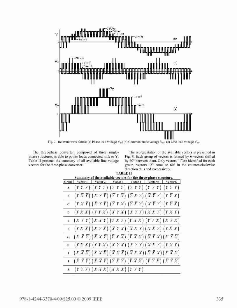
Fig. 7. Relevant wave forms: (a) Phase load voltage Van; (b) Common mode voltage Vn0; (c) Line load voltage Vab.
The three-phase converter, composed of three single-
phase structures, is able to power loads connected in Δ or Y. Table II presents the summary of all available line voltage vectors for the three-phase converter.
The representation of the available vectors is presented in Fig. 8. Each group of vectors is formed by 6 vectors shifted by 60° between them. Only vectors “1”are identified for each group, vectors “2” come to 60° in the counter-clockwise direction thus and successively.
TABLE II Summary of the available vectors for the three-phase structure.
Group Vector 1 Vector 2 Vector 3 Vector 4 Vector 5 Vector 6
A ( ) Y Y Y ( ) Y Y Y ( ) Y Y Y ( ) Y Y Y ( ) Y Y Y ( ) Y Y Y
B ( ) Y X Y ( ) X Y Y ( ) Y Y X ( ) Y X Y ( ) X Y Y ( ) Y Y X
C ( ) Y X Y
( ) X Y Y ( ) Y Y X ( ) Y X Y ( ) X Y Y ( ) Y Y X
D ( ) Y X X ( ) Y Y X ( ) X Y X ( ) X Y Y ( ) X X Y ( ) Y X Y
E ( ) X Y Y
( ) X X Y ( ) Y X Y ( ) Y X X ( ) Y Y X ( ) X Y X
F ( ) Y X X ( ) X Y X ( ) X Y X ( ) X X Y ( ) X X Y ( ) Y X X
G ( ) X X Y
( ) X X Y ( ) Y X X ( ) Y X X ( ) X Y X ( ) X Y X
H ( ) Y X X ( ) Y Y X ( ) X Y X ( ) X Y Y ( ) X X Y ( ) Y X Y
I ( ) X X X
( ) X X X ( ) X X X ( ) X X X ( ) X X X ( ) X X X
J ( ) X Y Y ( ) X X Y ( ) Y X Y ( ) Y X X ( ) Y Y X ( ) X Y X
Z ( ) Y Y Y
( ) X X X ( ) X X X ( ) Y Y Y
978-1-4244-3370-4/09/$25.00 © 2009 IEEE 335
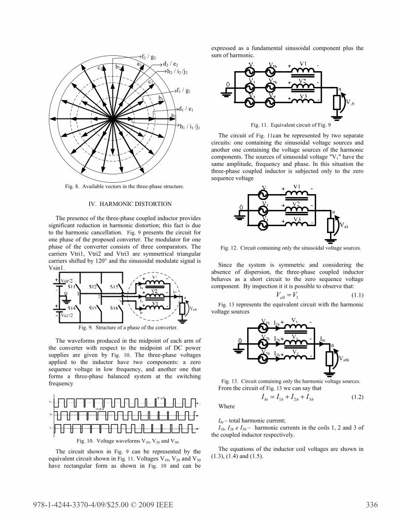
a1
b1
c1
f1 / g1
h1 / i1 /j1
d1 / e1
a2
h2 / i2 /j2
d2 / e2c2 b2
f2 / g2
Fig. 8. Available vectors in the three-phase structure.
IV. HARMONIC DISTORTION The presence of the three-phase coupled inductor provides
significant reduction in harmonic distortion; this fact is due to the harmonic cancellation. Fig. 9 presents the circuit for one phase of the proposed converter. The modulator for one phase of the converter consists of three comparators. The carriers Vtri1, Vtri2 and Vtri3 are symmetrical triangular carriers shifted by 120° and the sinusoidal modulate signal is Vsin1.
Fig. 9. Structure of a phase of the converter.
The waveforms produced in the midpoint of each arm of
the converter with respect to the midpoint of DC power supplies are given by Fig. 10. The three-phase voltages applied to the inductor have two components: a zero sequence voltage in low frequency, and another one that forms a three-phase balanced system at the switching frequency
Fig. 10. Voltage waveforms V10, V20 and V30.
The circuit shown in Fig. 9 can be represented by the equivalent circuit shown in Fig. 11. Voltages V10, V20 and V30 have rectangular form as shown in Fig. 10 and can be
expressed as a fundamental sinusoidal component plus the sum of harmonic.
Fig. 11. Equivalent circuit of Fig. 9
The circuit of Fig. 11can be represented by two separate circuits: one containing the sinusoidal voltage sources and another one containing the voltage sources of the harmonic components. The sources of sinusoidal voltage "V1" have the same amplitude, frequency and phase. In this situation the three-phase coupled inductor is subjected only to the zero sequence voltage
Fig. 12. Circuit containing only the sinusoidal voltage sources.
Since the system is symmetric and considering the absence of dispersion, the three-phase coupled inductor behaves as a short circuit to the zero sequence voltage component. By inspection it it is possible to observe that:
Fig. 13 represents the equivalent circuit with the harmonic voltage sources
a
Va0h
0
-+ Vx
Vy
Vz
-+
+ -
V1h
V2h
V3h
Iht
I1h
I2h
I3h
Fig. 13. Circuit containing only the harmonic voltage sources.
From the circuit of Fig. 13 we can say that
Where Iht – total harmonic current; I1h, I2h e I3h – harmonic currents in the coils 1, 2 and 3 of
the coupled inductor respectively. The equations of the inductor coil voltages are shown in
(1.3), (1.4) and (1.5).
0 1aV V= (1.1)
1 2 3ht h h hI I I I= + + (1.2)
978-1-4244-3370-4/09/$25.00 © 2009 IEEE 336
Where Vx, Vy e Vz – voltages in coils 1, 2 and 3 of the coupled
inductor respectively; L – inductance of each coil of the coupled inductor; M – mutual inductance between the coils of the coupled
inductor. The load voltage can then be written as
The coils voltages of the inductor are described by (1.7).
Or
For the ideal three-phase inductor:
Soon
This implies that
The substitution of (1.11) in (1.6) results:
Or
Voltages in the midpoint of each arm shown in Fig. 9 can be represented as:
The resulting voltage on the load considering one phase of the converter is then the sum of the voltages of the midpoint of each arm. The equation (1.17) shows that the harmonics contents in the load voltage will always be multiple of 3 when compared to the switching frequency.
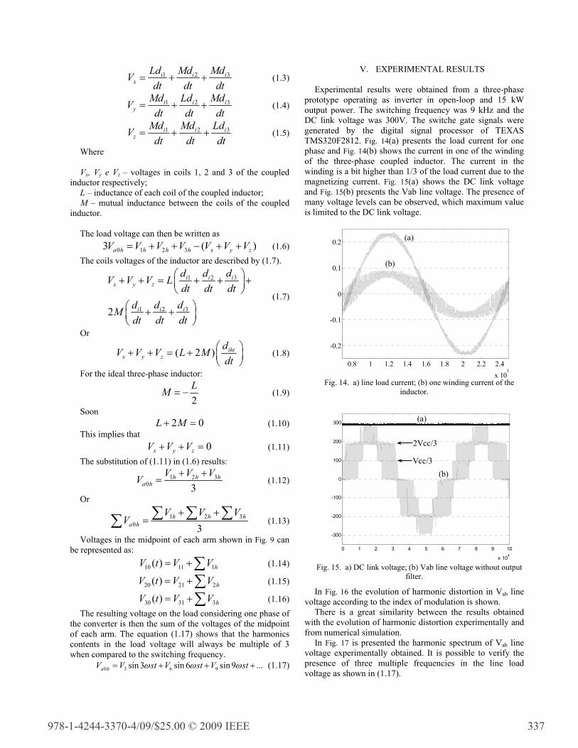
V. EXPERIMENTAL RESULTS Experimental results were obtained from a three-phase
prototype operating as inverter in open-loop and 15 kW output power. The switching frequency was 9 kHz and the DC link voltage was 300V. The switche gate signals were generated by the digital signal processor of TEXAS TMS320F2812. Fig. 14(a) presents the load current for one phase and Fig. 14(b) shows the current in one of the winding of the three-phase coupled inductor. The current in the winding is a bit higher than 1/3 of the load current due to the magnetizing current. Fig. 15(a) shows the DC link voltage and Fig. 15(b) presents the Vab line voltage. The presence of many voltage levels can be observed, which maximum value is limited to the DC link voltage.
0.8 1 1.2 1.4 1.6 1.8 2 2.2 2.4x 10
5
-0.2
-0.1
0
0.1
0.2 (a)
(b)
Fig. 14. a) line load current; (b) one winding current of the
inductor.
0 1 2 3 4 5 6 7 8 9 10
x 104
-300
-200
-100
0
100
200
300 (a)
(b)Vcc/3
2Vcc/3
Fig. 15. a) DC link voltage; (b) Vab line voltage without output
filter.
In Fig. 16 the evolution of harmonic distortion in Vab line voltage according to the index of modulation is shown.
There is a great similarity between the results obtained with the evolution of harmonic distortion experimentally and from numerical simulation.
In Fig. 17 is presented the harmonic spectrum of Vab line voltage experimentally obtained. It is possible to verify the presence of three multiple frequencies in the line load voltage as shown in (1.17).
1 2 3i i ix
Ld Md MdVdt dt dt
= + + (1.3)
1 2 3i i iy
Md Ld MdVdt dt dt
= + + (1.4)
1 2 3i i iz
Md Md LdVdt dt dt
= + + (1.5)
0 1 2 33 ( )a h h h h x y zV V V V V V V= + + − + + (1.6)
1 2 3
1 2 32
i i ix y z
i i i
d d dV V V Ldt dt dt
d d dMdt dt dt
⎛ ⎞+ + = + + +⎜ ⎟⎝ ⎠
⎛ ⎞+ +⎜ ⎟⎝ ⎠
(1.7)
( 2 ) ihtx y z
dV V V L Mdt
⎛ ⎞+ + = + ⎜ ⎟⎝ ⎠
(1.8)
2LM = − (1.9)
2 0L M+ = (1.10)
0x y zV V V+ + = (1.11)
1 2 30 3
h h ha h
V V VV + += (1.12)
1 2 30 3
h h ha h
V V VV
+ += ∑ ∑ ∑∑ (1.13)
10 11 1( ) hV t V V= +∑ (1.14)
20 21 2( ) hV t V V= +∑ (1.15)
30 31 3( ) hV t V V= +∑ (1.16)
0 3 6 9sin 3 sin 6 sin 9 ...a hV V st V st V stω ω ω= + + + (1.17)
978-1-4244-3370-4/09/$25.00 © 2009 IEEE 337
0
10
20
30
40
50
60
70
0,5 0,55 0,6 0,65 0,7 0,75 0,8 0,85 0,9
TH
D o
f Vab
lin
e vo
ltage
(%)
Modulation index
Simulation result
Experimental result
Fig. 16. Evolution of the harmonic distortion of the Vab voltage
according to the modulation index.
9KHz 27KHz 54KHz 81KHz0
5
10
15
20
Frequency(Hz)
Fig. 17. Harmonic spectrum of Vab line voltage - experimental results
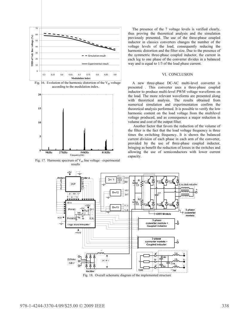
The presence of the 7 voltage levels is verified clearly, thus proving the theoretical analysis and the simulation previously presented. The use of the three-phase coupled inductor in classics converters changes the number of the voltage levels of the load, consequently reducing the harmonic distortion and the filter size. Due to the presence of the symmetric three-phase coupled inductor, the current in each leg to one phase of the converter divides in a balanced way and is equal to 1/3 of the load phase current.
VI. CONCLUSION A new three-phase DC-AC multi-level converter is
presented . This converter uses a three-phase coupled inductor to produce multi-level PWM voltage waveforms on the load. The more relevant waveforms are presented along with theoretical analysis. The results obtained from numerical simulation and experimentation confirm the theoretical analysis performed. It is possible to verify the low harmonic content on the load voltage from the multilevel voltage produced, and as consequence a major reduction in volume and cost of the output filter.
Another factor that favors the reduction of the volume of the filter is the fact that the load voltage frequency is three times the switching frequency. It is shown the balanced current division of each phase in each arm of the converter, provided by the use of three-phase coupled inductor, bringing as benefit the reduction of losses in the switches and allowing the use of semiconductors with lower current capacity.
Fig. 18. Overall schematic diagram of the implemented structure
978-1-4244-3370-4/09/$25.00 © 2009 IEEE 338
(a)
(b)
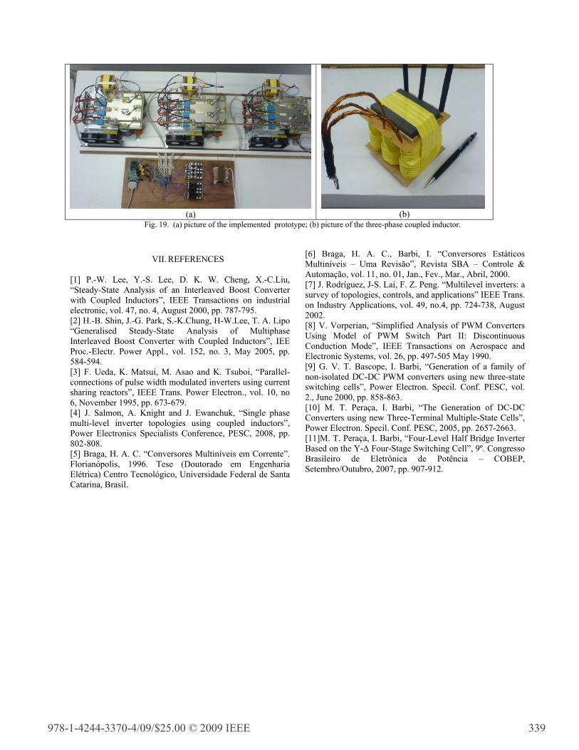
Fig. 19. (a) picture of the implemented prototype; (b) picture of the three-phase coupled inductor.
VII. REFERENCES
[1] P.-W. Lee, Y.-S. Lee, D. K. W. Cheng, X.-C.Liu, “Steady-State Analysis of an Interleaved Boost Converter with Coupled Inductors”, IEEE Transactions on industrial electronic, vol. 47, no. 4, August 2000, pp. 787-795. [2] H.-B. Shin, J.-G. Park, S.-K.Chung, H-W.Lee, T. A. Lipo “Generalised Steady-State Analysis of Multiphase Interleaved Boost Converter with Coupled Inductors”, IEE Proc.-Electr. Power Appl., vol. 152, no. 3, May 2005, pp. 584-594. [3] F. Ueda, K. Matsui, M. Asao and K. Tsuboi, “Parallel-connections of pulse width modulated inverters using current sharing reactors”, IEEE Trans. Power Electron., vol. 10, no 6, November 1995, pp. 673-679. [4] J. Salmon, A. Knight and J. Ewanchuk, “Single phase multi-level inverter topologies using coupled inductors”, Power Electronics Specialists Conference, PESC, 2008, pp. 802-808. [5] Braga, H. A. C. “Conversores Multiníveis em Corrente”. Florianópolis, 1996. Tese (Doutorado em Engenharia Elétrica) Centro Tecnológico, Universidade Federal de Santa Catarina, Brasil.
[6] Braga, H. A. C., Barbi, I. “Conversores Estáticos Multiníveis – Uma Revisão”, Revista SBA – Controle & Automação, vol. 11, no. 01, Jan., Fev., Mar., Abril, 2000. [7] J. Rodríguez, J-S. Lai, F. Z. Peng. “Multilevel inverters: a survey of topologies, controls, and applications” IEEE Trans. on Industry Applications, vol. 49, no.4, pp. 724-738, August 2002. [8] V. Vorperian, “Simplified Analysis of PWM Converters Using Model of PWM Switch Part II: Discontinuous Conduction Mode”, IEEE Transactions on Aerospace and Electronic Systems, vol. 26, pp. 497-505 May 1990. [9] G. V. T. Bascope, I. Barbi, “Generation of a family of non-isolated DC-DC PWM converters using new three-state switching cells”, Power Electron. Specil. Conf. PESC, vol. 2., June 2000, pp. 858-863. [10] M. T. Peraça, I. Barbi, “The Generation of DC-DC Converters using new Three-Terminal Multiple-State Cells”, Power Electron. Specil. Conf. PESC, 2005, pp. 2657-2663. [11]M. T. Peraça, I. Barbi, “Four-Level Half Bridge Inverter Based on the Y-Δ Four-Stage Switching Cell”, 9º. Congresso Brasileiro de Eletrônica de Potência – COBEP, Setembro/Outubro, 2007, pp. 907-912.
978-1-4244-3370-4/09/$25.00 © 2009 IEEE 339