Embed Size (px)
Citation preview

Title:- 4 BIT ARITHMETIC AND LOGICAL UNIT
Theory :-
Arithmetic Logic Unit is a common operational unit with number of storage
registers connected to it, using which it performs micro operations. To perform
a micro operation, the contents of specified registers are placed in the inputs
of the common ALU. The ALU performs an operation and the result of the
operation is then transferred to a destination register. The ALU is a
combinational circuit so that the entire registers transfer operation from the
source register through the ALU and the destination register can be performed
during one clock pulse period.
One stage ALU Truth Table of ALU
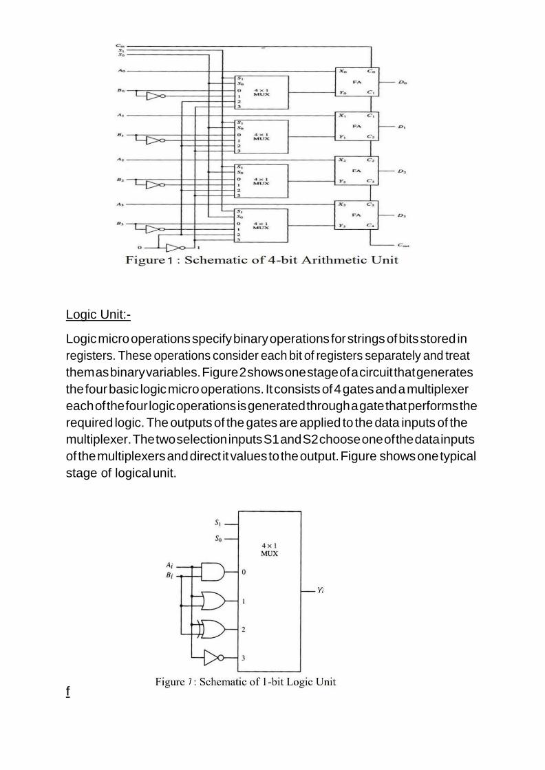
Arithmetic Unit :-
The arithmetic operations in the table can be implemented in one composite
arithmetic circuit. The basic component of an arithmetic circuit is a full adder.
By controlling the data input to the adder it is possible to obtain different types
of arithmetic operations. The diagram of the 4-bit arithmetic circuit is shown in
figure 1. It has four full adder circuits that constitute the 4 bit adder and 4
multiplexers for choosing multiple operations. There are two 4 bit inputs A and
B and 4 bit output D.
Logic Unit:-
Logic micro operations specify binary operations for strings of bits stored in
registers. These operations consider each bit of registers separately and treat
them as binary variables. Figure 2 shows one stage of a circuit that generates
the four basic logic micro operations. It consists of 4 gates and a multiplexer
each of the four logic operations is generated through a gate that performs the
required logic. The outputs of the gates are applied to the data inputs of the
multiplexer. The two selection inputs S1 and S2 choose one of the data inputs
of the multiplexers and direct it values to the output. Figure shows one typical
stage of logical unit.
f
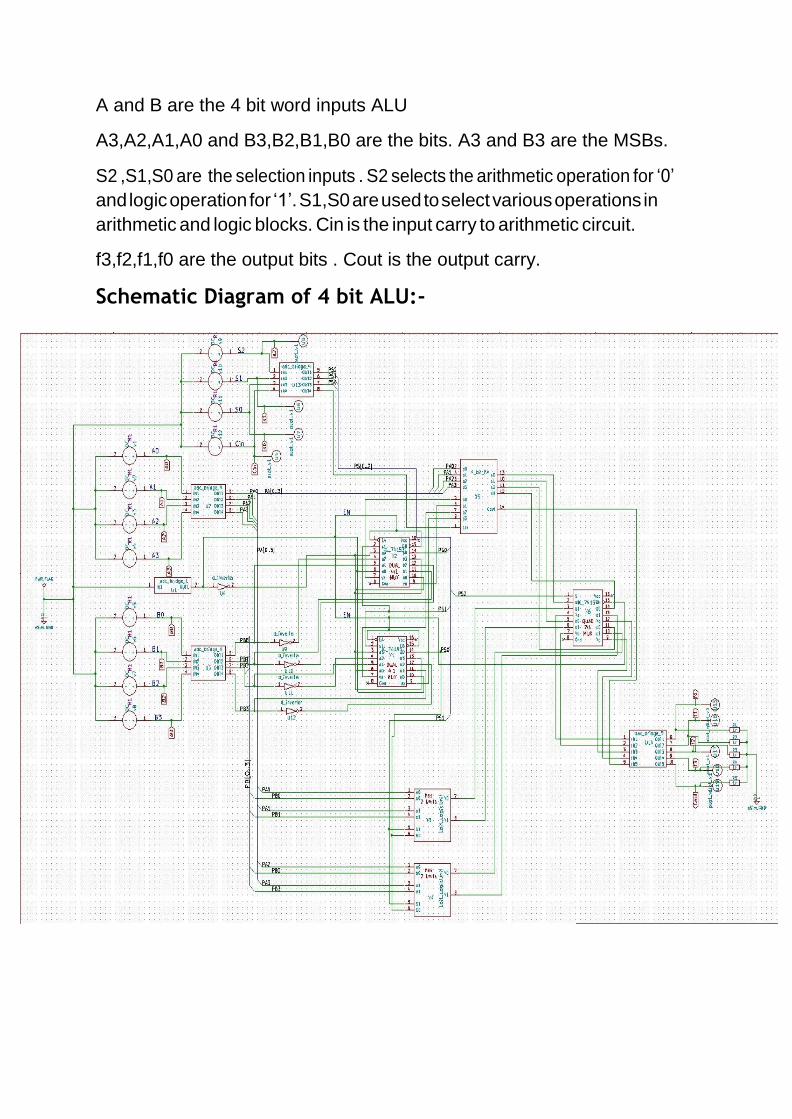
A and B are the 4 bit word inputs ALU
A3,A2,A1,A0 and B3,B2,B1,B0 are the bits. A3 and B3 are the MSBs.
S2 ,S1,S0 are the selection inputs . S2 selects the arithmetic operation for ‘0’
and logic operation for ‘1’. S1,S0 are used to select various operations in
arithmetic and logic blocks. Cin is the input carry to arithmetic circuit.
f3,f2,f1,f0 are the output bits . Cout is the output carry.
Schematic Diagram of 4 bit ALU:-
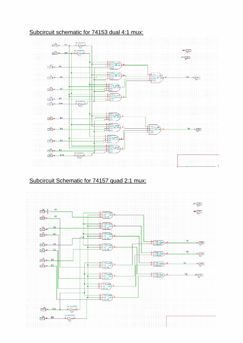
Subcircuit schematic for 74153 dual 4:1 mux:
Subcircuit Schematic for 74157 quad 2:1 mux:
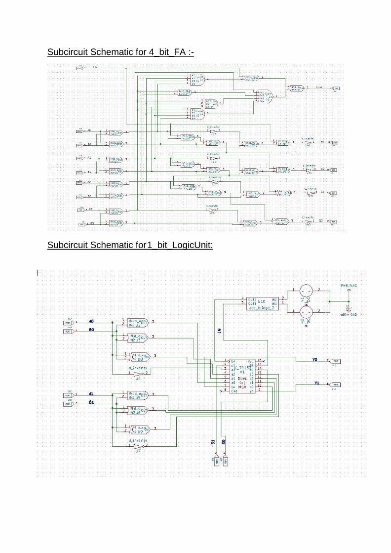
Subcircuit Schematic for 4_bit_FA :-
Subcircuit Schematic for 1_bit_LogicUnit:

A Value Voltage
Source
Value
(v)
3 1 V4 5
2 0 V3 0
1 0 V2 0
0 1 V1 5
B Value Voltage
Source
Value
(v)
3 1 V8 5
2 0 V7 0
1 1 V6 5
0 0 V5 0
Simulation Results:-
Input:-
A[3 : 0] – 1 0 0 1 B[3 : 0] – 1 0 1 0
Input Voltage
source
S2 V9
S1 V10
S0 V11
Cin V12
Output when S2 = ‘ 0 ‘ -- v9 = 0v
S1 = ‘ 0 ‘ -- v10 = 0 v operation performed
S0 = ‘ 1 ‘ -- v11 = 5v is ADD with carry
Cin = ‘ 1 ‘ -- v12 = 5 v F= A+B+1
F[3 : 0] – 0 1 0 0 Cout = ‘ 1 ‘
NGSPICE PLOTS:-
Cout
f0 f1
f2 f3
PYTHON PLOTS:-
f0 f1
f2 f3
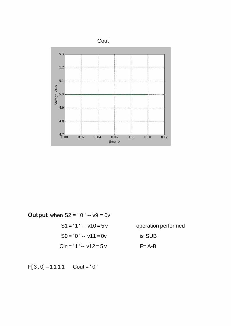
Cout
Output when S2 = ‘ 0 ‘ -- v9 = 0v
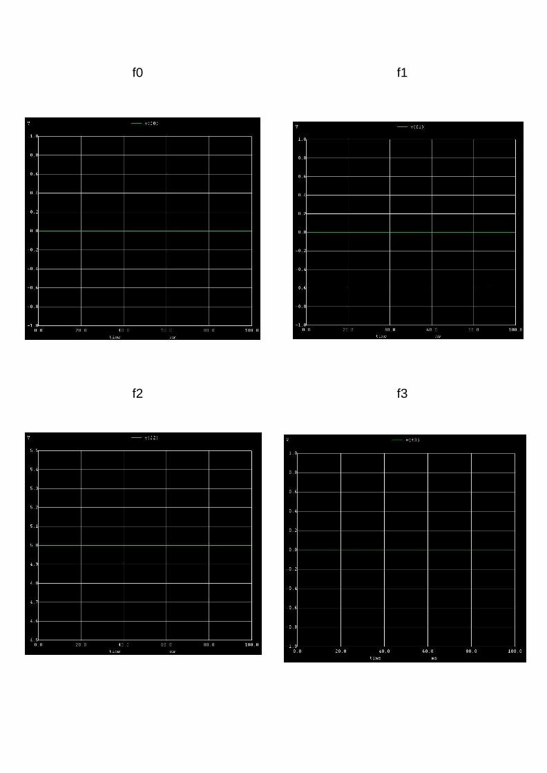
S1 = ‘ 1 ‘ -- v10 = 5 v operation performed
S0 = ‘ 0 ‘ -- v11 = 0v is SUB
Cin = ‘ 1 ‘ -- v12 = 5 v F= A-B
F[ 3 : 0] – 1 1 1 1 Cout = ‘ 0 ‘
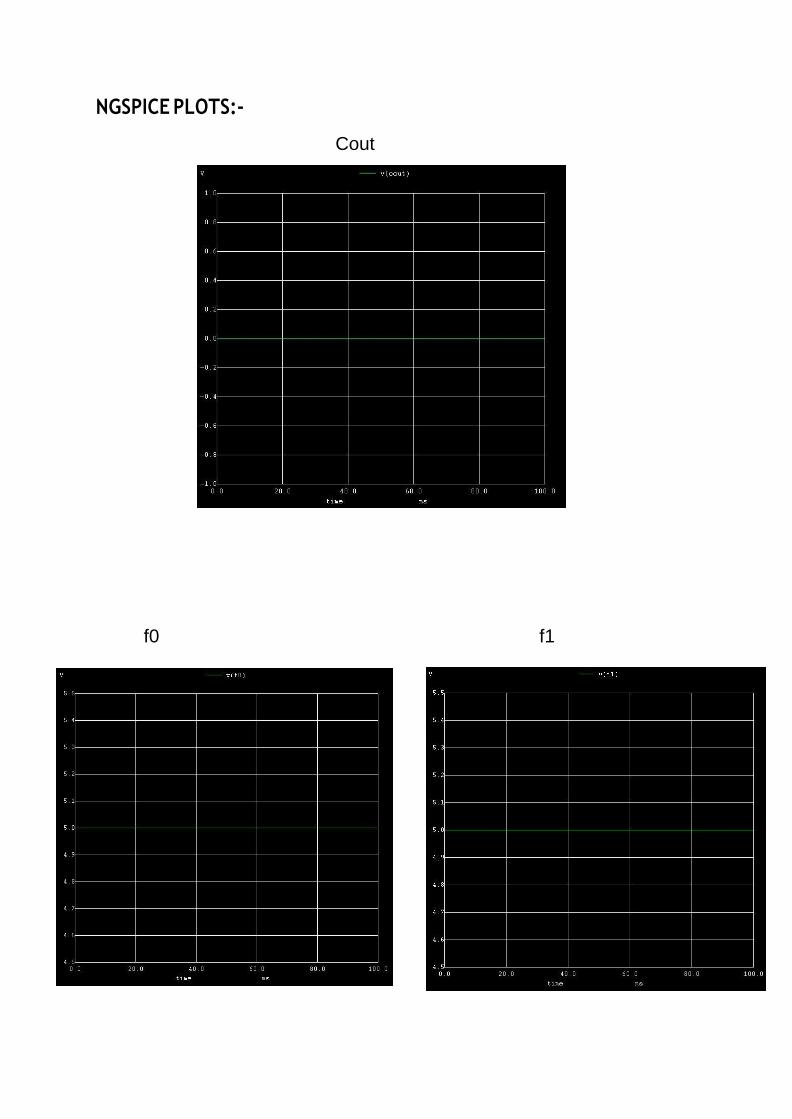
NGSPICE PLOTS:-
Cout
f0 f1
f2 f3
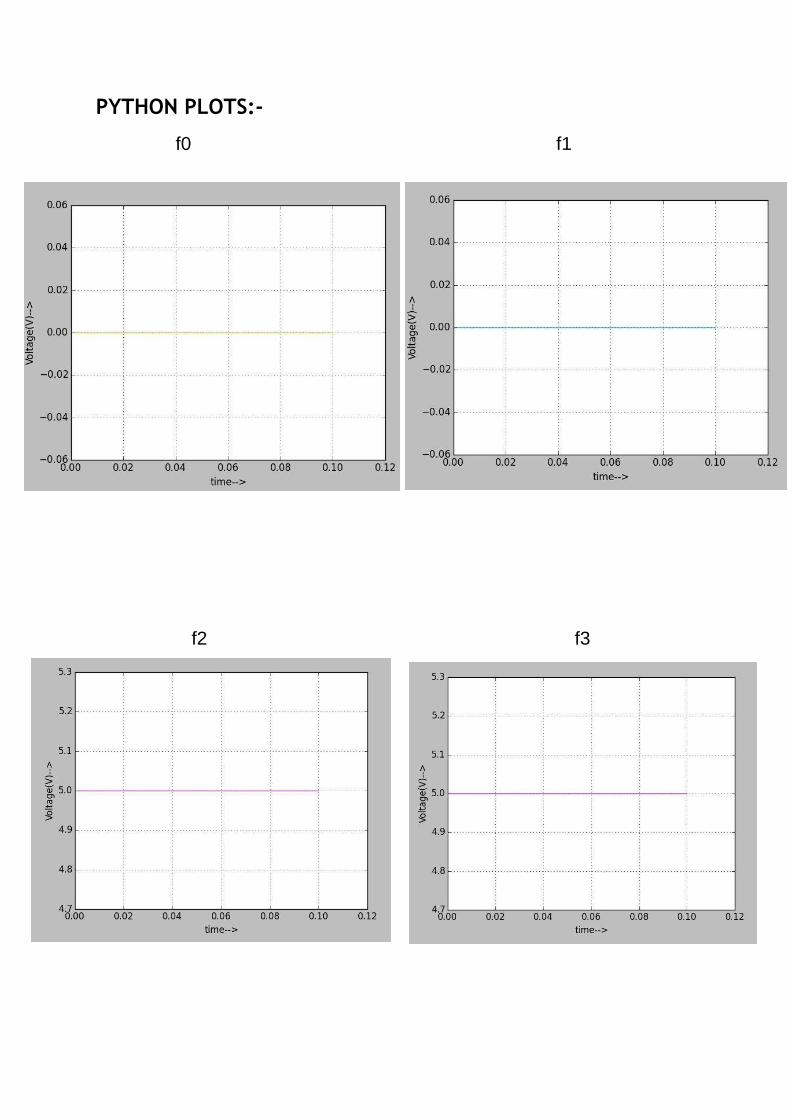
PYTHON PLOTS:-
Cout
f0 f1
f2 f3
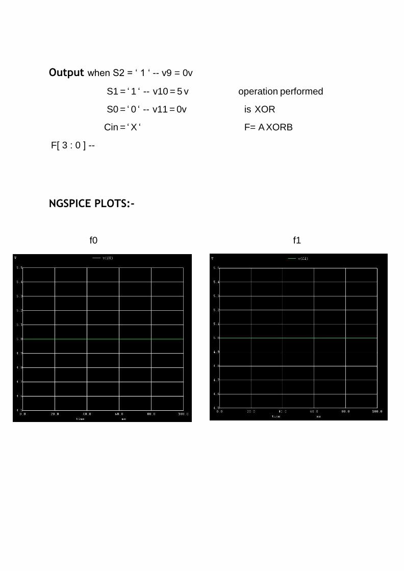
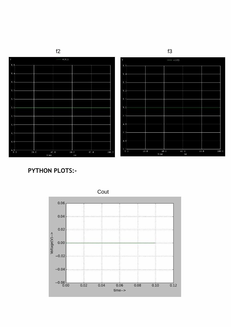
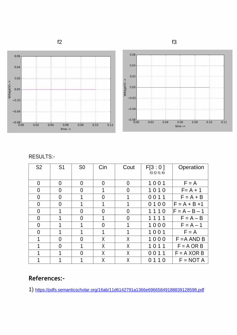
Output when S2 = ‘ 1 ‘ -- v9 = 0v
S1 = ‘ 1 ‘ -- v10 = 5 v operation performed
S0 = ‘ 0 ‘ -- v11 = 0v is XOR
Cin = ‘ X ‘ F= A XORB
F[ 3 : 0 ] --
NGSPICE PLOTS:-
f0 f1
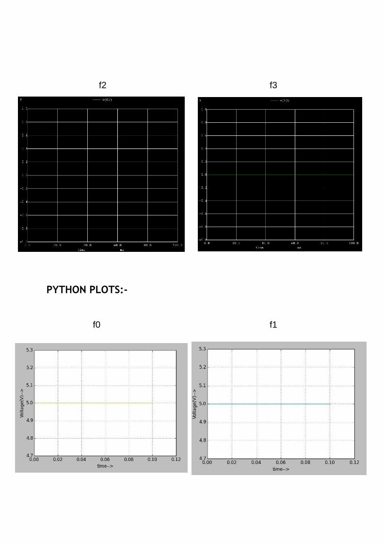
f2 f3
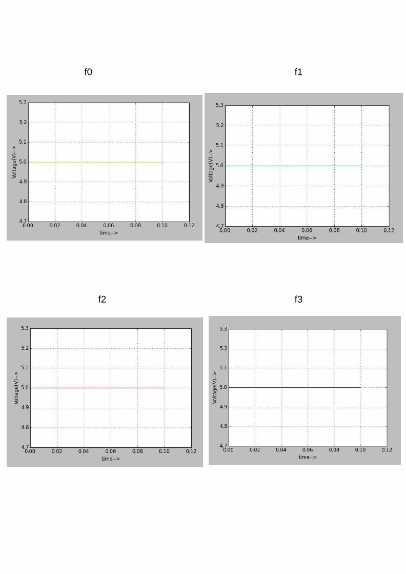
PYTHON PLOTS:-
f0 f1
f2 f3
RESULTS:-
S2 S1 S0 Cin Cout F[3 : 0 ] f3 f2 f1 f0
Operatiion
0 0 0 0 0 1 0 0 1 F = A
0 0 0 1 0 1 0 1 0 F= A + 1
0 0 1 0 1 0 0 1 1 F = A + B
0 0 1 1 1 0 1 0 0 F = A + B +1
0 1 0 0 0 1 1 1 0 F = A – B – 1
0 1 0 1 0 1 1 1 1 F = A – B
0 1 1 0 1 1 0 0 0 F = A – 1
0 1 1 1 1 1 0 0 1 F = A
1 0 0 X X 1 0 0 0 F = A AND B
1 0 1 X X 1 0 1 1 F = A OR B
1 1 0 X X 0 0 1 1 F = A XOR B
1 1 1 X X 0 1 1 0 F = NOT A
References:-
1) https://pdfs.semanticscholar.org/16ab/11d6142791a1366e69665849188839128598.pdf