Embed Size (px)
Citation preview
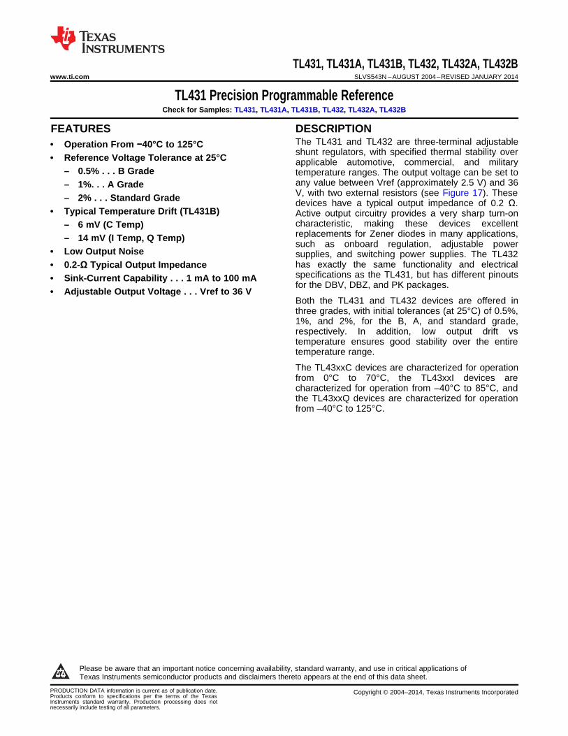
TL431, TL431A, TL431B, TL432, TL432A, TL432Bwww.ti.com SLVS543N –AUGUST 2004–REVISED JANUARY 2014
TL431 Precision Programmable ReferenceCheck for Samples: TL431, TL431A, TL431B, TL432, TL432A, TL432B
1FEATURES DESCRIPTIONThe TL431 and TL432 are three-terminal adjustable• Operation From −40°C to 125°Cshunt regulators, with specified thermal stability over• Reference Voltage Tolerance at 25°C applicable automotive, commercial, and military
– 0.5% . . . B Grade temperature ranges. The output voltage can be set toany value between Vref (approximately 2.5 V) and 36– 1%. . . A GradeV, with two external resistors (see Figure 17). These– 2% . . . Standard Grade devices have a typical output impedance of 0.2 Ω.
• Typical Temperature Drift (TL431B) Active output circuitry provides a very sharp turn-oncharacteristic, making these devices excellent– 6 mV (C Temp)replacements for Zener diodes in many applications,– 14 mV (I Temp, Q Temp) such as onboard regulation, adjustable power
• Low Output Noise supplies, and switching power supplies. The TL432has exactly the same functionality and electrical• 0.2-Ω Typical Output Impedancespecifications as the TL431, but has different pinouts• Sink-Current Capability . . . 1 mA to 100 mAfor the DBV, DBZ, and PK packages.
• Adjustable Output Voltage . . . Vref to 36 VBoth the TL431 and TL432 devices are offered inthree grades, with initial tolerances (at 25°C) of 0.5%,1%, and 2%, for the B, A, and standard grade,respectively. In addition, low output drift vstemperature ensures good stability over the entiretemperature range.
The TL43xxC devices are characterized for operationfrom 0°C to 70°C, the TL43xxI devices arecharacterized for operation from –40°C to 85°C, andthe TL43xxQ devices are characterized for operationfrom –40°C to 125°C.
1
Please be aware that an important notice concerning availability, standard warranty, and use in critical applications ofTexas Instruments semiconductor products and disclaimers thereto appears at the end of this data sheet.
PRODUCTION DATA information is current as of publication date. Copyright © 2004–2014, Texas Instruments IncorporatedProducts conform to specifications per the terms of the TexasInstruments standard warranty. Production processing does notnecessarily include testing of all parameters.
CATHODE
ANODE
REF
TL431 . . . KTP (PowerFLEX /TO-252) PACKAGE
(TOP VIEW)
AN
OD
E
TL431A, TL431B . . . DCK (SC-70) PACKAGE
(TOP VIEW)
1
2
3
6
5
4
CATHODE
NC
REF
ANODE
NC
NC
NC − No internal connection
TL431, TL431A, TL431B . . . LP (TO-92/TO-226) PACKAGE
(TOP VIEW)
CATHODE
ANODE
REF
1
2
3
4
8
7
6
5
CATHODE
ANODE
ANODE
NC
REF
ANODE
ANODE
NC
TL431, TL431A, TL431B . . . D (SOIC) PACKAGE
(TOP VIEW)
1
2
3
4
8
7
6
5
CATHODE
NC
NC
NC
REF
NC
ANODE
NC
TL431, TL431A, TL431B . . . P (PDIP), PS (SOP),
OR PW (TSSOP) PACKAGE
(TOP VIEW)
NC − No internal connection
TL431, TL431A, TL431B . . . DBV (SOT-23-5) PACKAGE
(TOP VIEW)
1
2
3
5
4
NC
†
CATHODE
ANODE
REF
TL431, TL431A, TL431B . . . PK (SOT-89) PACKAGE
(TOP VIEW)
REF
ANODE
CATHODE
† Pin 2 is attached to Substrate and must be
connected to ANODE or left open.
NC − No internal connection
TL432, TL432A, TL432B . . . DBV (SOT-23-5) PACKAGE
(TOP VIEW)
1
2
3
5
4
NC
ANODE
NC
REF
CATHODE
NC − No internal connection
TL431, TL431A, TL431B . . . DBZ (SOT-23-3) PACKAGE
(TOP VIEW)
TL432, TL432A, TL432B . . . DBZ (SOT-23-3) PACKAGE
(TOP VIEW)
NC − No internal connection
1
2
3
REF
CATHODE
ANODE
1
2
3
CATHODE
REF
ANODE
AN
OD
E
TL432, TL432A, TL432B . . . PK (SOT-89) PACKAGE
(TOP VIEW)
REF
ANODE
CATHODE
AN
OD
E
TL431, TL431A, TL431B, TL432, TL432A, TL432BSLVS543N –AUGUST 2004–REVISED JANUARY 2014 www.ti.com
2 Submit Documentation Feedback Copyright © 2004–2014, Texas Instruments Incorporated
Product Folder Links :TL431 TL431A TL431B TL432 TL432A TL432B

ANODE
REF
CATHODE
2.4 kΩ 7.2 kΩ
3.28 kΩ
20 pF
4 kΩ
1 kΩ
800 Ω
800 Ω 800 Ω
20 pF
150 Ω
10 kΩ
CATHODE
REF
ANODE
+
_
Vref
REF
CATHODEANODE
TL431, TL431A, TL431B, TL432, TL432A, TL432Bwww.ti.com SLVS543N –AUGUST 2004–REVISED JANUARY 2014
Symbol
Functional Block Diagram
Equivalent Schematic
NOTE: All component values are nominal.
Copyright © 2004–2014, Texas Instruments Incorporated Submit Documentation Feedback 3
Product Folder Links :TL431 TL431A TL431B TL432 TL432A TL432B
TL431, TL431A, TL431B, TL432, TL432A, TL432BSLVS543N –AUGUST 2004–REVISED JANUARY 2014 www.ti.com
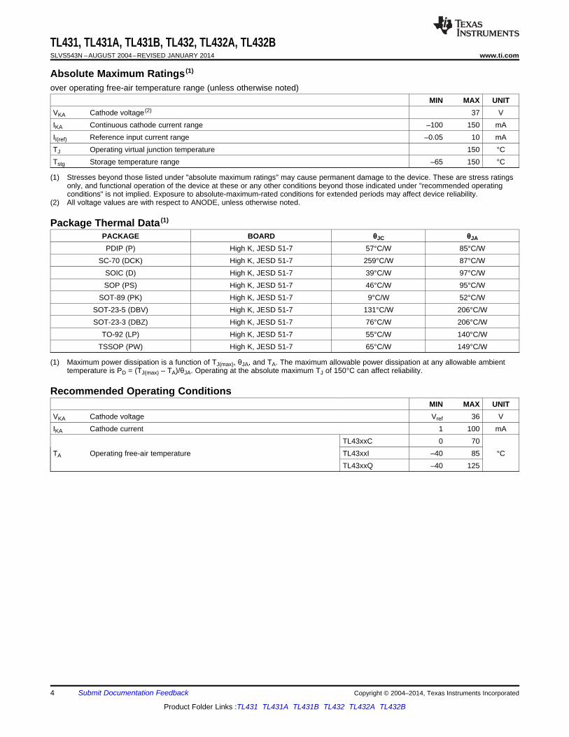
Absolute Maximum Ratings (1)
over operating free-air temperature range (unless otherwise noted)MIN MAX UNIT
VKA Cathode voltage (2) 37 VIKA Continuous cathode current range –100 150 mAII(ref) Reference input current range –0.05 10 mATJ Operating virtual junction temperature 150 °CTstg Storage temperature range –65 150 °C
(1) Stresses beyond those listed under "absolute maximum ratings" may cause permanent damage to the device. These are stress ratingsonly, and functional operation of the device at these or any other conditions beyond those indicated under "recommended operatingconditions" is not implied. Exposure to absolute-maximum-rated conditions for extended periods may affect device reliability.
(2) All voltage values are with respect to ANODE, unless otherwise noted.
Package Thermal Data (1)
PACKAGE BOARD θJC θJA
PDIP (P) High K, JESD 51-7 57°C/W 85°C/WSC-70 (DCK) High K, JESD 51-7 259°C/W 87°C/W
SOIC (D) High K, JESD 51-7 39°C/W 97°C/WSOP (PS) High K, JESD 51-7 46°C/W 95°C/W
SOT-89 (PK) High K, JESD 51-7 9°C/W 52°C/WSOT-23-5 (DBV) High K, JESD 51-7 131°C/W 206°C/WSOT-23-3 (DBZ) High K, JESD 51-7 76°C/W 206°C/W
TO-92 (LP) High K, JESD 51-7 55°C/W 140°C/WTSSOP (PW) High K, JESD 51-7 65°C/W 149°C/W
(1) Maximum power dissipation is a function of TJ(max), θJA, and TA. The maximum allowable power dissipation at any allowable ambienttemperature is PD = (TJ(max) – TA)/θJA. Operating at the absolute maximum TJ of 150°C can affect reliability.
Recommended Operating ConditionsMIN MAX UNIT
VKA Cathode voltage Vref 36 VIKA Cathode current 1 100 mA
TL43xxC 0 70TA Operating free-air temperature TL43xxI –40 85 °C
TL43xxQ –40 125
4 Submit Documentation Feedback Copyright © 2004–2014, Texas Instruments Incorporated
Product Folder Links :TL431 TL431A TL431B TL432 TL432A TL432B
R2R1|z |KA (1 + (
∆I∆V|z'| =
∆IKA
∆VKA|z | =KA(2) The dynamic impedance is defined as:
When the device is operating with two external resistors (see Figure 2), the total dynamic impedance of the circuit is given by:
which is approximately equal to .
TL431, TL431A, TL431B, TL432, TL432A, TL432Bwww.ti.com SLVS543N –AUGUST 2004–REVISED JANUARY 2014
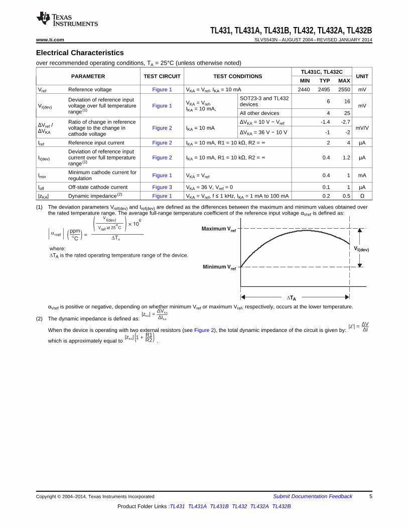
Electrical Characteristicsover recommended operating conditions, TA = 25°C (unless otherwise noted)
TL431C, TL432CPARAMETER TEST CIRCUIT TEST CONDITIONS UNIT
MIN TYP MAXVref Reference voltage Figure 1 VKA = Vref, IKA = 10 mA 2440 2495 2550 mV
SOT23-3 and TL432Deviation of reference input 6 16VKA = Vref, devicesVI(dev) voltage over full temperature Figure 1 mVIKA = 10 mA,range (1) All other devices 4 25Ratio of change in reference ΔVKA = 10 V − Vref -1.4 -2.7ΔVref / voltage to the change in Figure 2 IKA = 10 mA mV/VΔVKA ΔVKA = 36 V − 10 V -1 -2cathode voltage
Iref Reference input current Figure 2 IKA = 10 mA, R1 = 10 kΩ, R2 = ∞ 2 4 µADeviation of reference input
II(dev) current over full temperature Figure 2 IKA = 10 mA, R1 = 10 kΩ, R2 = ∞ 0.4 1.2 µArange (1)
Minimum cathode current forImin Figure 1 VKA = Vref 0.4 1 mAregulationIoff Off-state cathode current Figure 3 VKA = 36 V, Vref = 0 0.1 1 µA|zKA| Dynamic impedance (2) Figure 1 VKA = Vref, f ≤ 1 kHz, IKA = 1 mA to 100 mA 0.2 0.5 Ω
(1) The deviation parameters Vref(dev) and Iref(dev) are defined as the differences between the maximum and minimum values obtained overthe rated temperature range. The average full-range temperature coefficient of the reference input voltage αVref is defined as:
αVref is positive or negative, depending on whether minimum Vref or maximum Vref, respectively, occurs at the lower temperature.
Copyright © 2004–2014, Texas Instruments Incorporated Submit Documentation Feedback 5
Product Folder Links :TL431 TL431A TL431B TL432 TL432A TL432B
R2R1|z |KA (1 + (
∆I∆V|z'| =
∆IKA
∆VKA|z | =KA(2) The dynamic impedance is defined as:
When the device is operating with two external resistors (see Figure 2), the total dynamic impedance of the circuit is given by:
which is approximately equal to .
TL431, TL431A, TL431B, TL432, TL432A, TL432BSLVS543N –AUGUST 2004–REVISED JANUARY 2014 www.ti.com
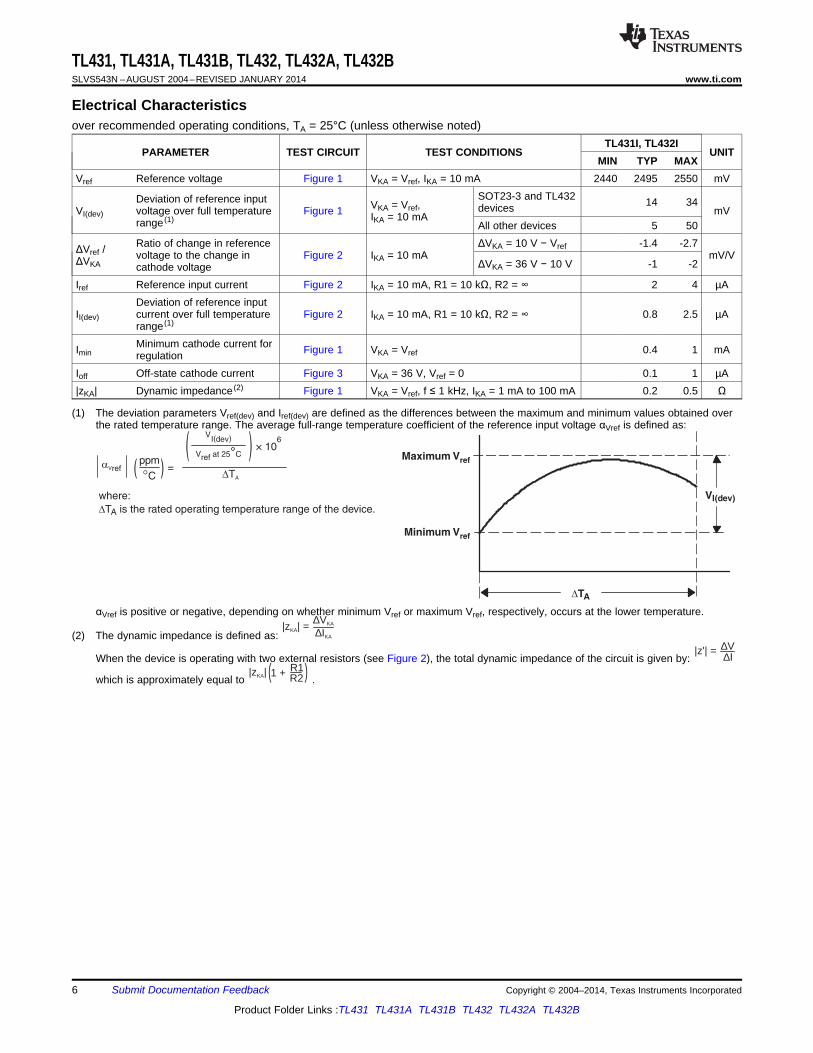
Electrical Characteristicsover recommended operating conditions, TA = 25°C (unless otherwise noted)
TL431I, TL432IPARAMETER TEST CIRCUIT TEST CONDITIONS UNIT
MIN TYP MAXVref Reference voltage Figure 1 VKA = Vref, IKA = 10 mA 2440 2495 2550 mV
SOT23-3 and TL432Deviation of reference input 14 34VKA = Vref, devicesVI(dev) voltage over full temperature Figure 1 mVIKA = 10 mArange (1) All other devices 5 50Ratio of change in reference ΔVKA = 10 V − Vref -1.4 -2.7ΔVref / voltage to the change in Figure 2 IKA = 10 mA mV/VΔVKA ΔVKA = 36 V − 10 V -1 -2cathode voltage
Iref Reference input current Figure 2 IKA = 10 mA, R1 = 10 kΩ, R2 = ∞ 2 4 µADeviation of reference input
II(dev) current over full temperature Figure 2 IKA = 10 mA, R1 = 10 kΩ, R2 = ∞ 0.8 2.5 µArange (1)
Minimum cathode current forImin Figure 1 VKA = Vref 0.4 1 mAregulationIoff Off-state cathode current Figure 3 VKA = 36 V, Vref = 0 0.1 1 µA|zKA| Dynamic impedance (2) Figure 1 VKA = Vref, f ≤ 1 kHz, IKA = 1 mA to 100 mA 0.2 0.5 Ω
(1) The deviation parameters Vref(dev) and Iref(dev) are defined as the differences between the maximum and minimum values obtained overthe rated temperature range. The average full-range temperature coefficient of the reference input voltage αVref is defined as:
αVref is positive or negative, depending on whether minimum Vref or maximum Vref, respectively, occurs at the lower temperature.
6 Submit Documentation Feedback Copyright © 2004–2014, Texas Instruments Incorporated
Product Folder Links :TL431 TL431A TL431B TL432 TL432A TL432B
R2R1|z |KA (1 + (
∆I∆V|z'| =
∆IKA
∆VKA|z | =KA(2) The dynamic impedance is defined as:
When the device is operating with two external resistors (see Figure 2), the total dynamic impedance of the circuit is given by:
which is approximately equal to .
TL431, TL431A, TL431B, TL432, TL432A, TL432Bwww.ti.com SLVS543N –AUGUST 2004–REVISED JANUARY 2014
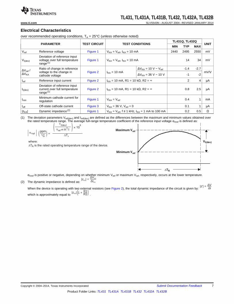
Electrical Characteristicsover recommended operating conditions, TA = 25°C (unless otherwise noted)
TL431Q, TL432QPARAMETER TEST CIRCUIT TEST CONDITIONS UNIT
MIN TYP MAXVref Reference voltage Figure 1 VKA = Vref, IKA = 10 mA 2440 2495 2550 mV
Deviation of reference inputVI(dev) voltage over full temperature Figure 1 VKA = Vref, IKA = 10 mA 14 34 mV
range (1)
Ratio of change in reference ΔVKA = 10 V − Vref -1.4 -2.7ΔVref / voltage to the change in Figure 2 IKA = 10 mA mV/VΔVKA ΔVKA = 36 V − 10 V -1 -2cathode voltageIref Reference input current Figure 2 IKA = 10 mA, R1 = 10 kΩ, R2 = ∞ 2 4 µA
Deviation of reference inputII(dev) current over full temperature Figure 2 IKA = 10 mA, R1 = 10 kΩ, R2 = ∞ 0.8 2.5 µA
range (1)
Minimum cathode current forImin Figure 1 VKA = Vref 0.4 1 mAregulationIoff Off-state cathode current Figure 3 VKA = 36 V, Vref = 0 0.1 1 µA|zKA| Dynamic impedance (2) Figure 1 VKA = Vref, f ≤ 1 kHz, IKA = 1 mA to 100 mA 0.2 0.5 Ω
(1) The deviation parameters Vref(dev) and Iref(dev) are defined as the differences between the maximum and minimum values obtained overthe rated temperature range. The average full-range temperature coefficient of the reference input voltage αVref is defined as:
αVref is positive or negative, depending on whether minimum Vref or maximum Vref, respectively, occurs at the lower temperature.
Copyright © 2004–2014, Texas Instruments Incorporated Submit Documentation Feedback 7
Product Folder Links :TL431 TL431A TL431B TL432 TL432A TL432B
R2R1|z |KA (1 + (
∆I∆V|z'| =
∆IKA
∆VKA|z | =KA(2) The dynamic impedance is defined as:
When the device is operating with two external resistors (see Figure 2), the total dynamic impedance of the circuit is given by:
which is approximately equal to .
TL431, TL431A, TL431B, TL432, TL432A, TL432BSLVS543N –AUGUST 2004–REVISED JANUARY 2014 www.ti.com
Electrical Characteristicsover recommended operating conditions, TA = 25°C (unless otherwise noted)
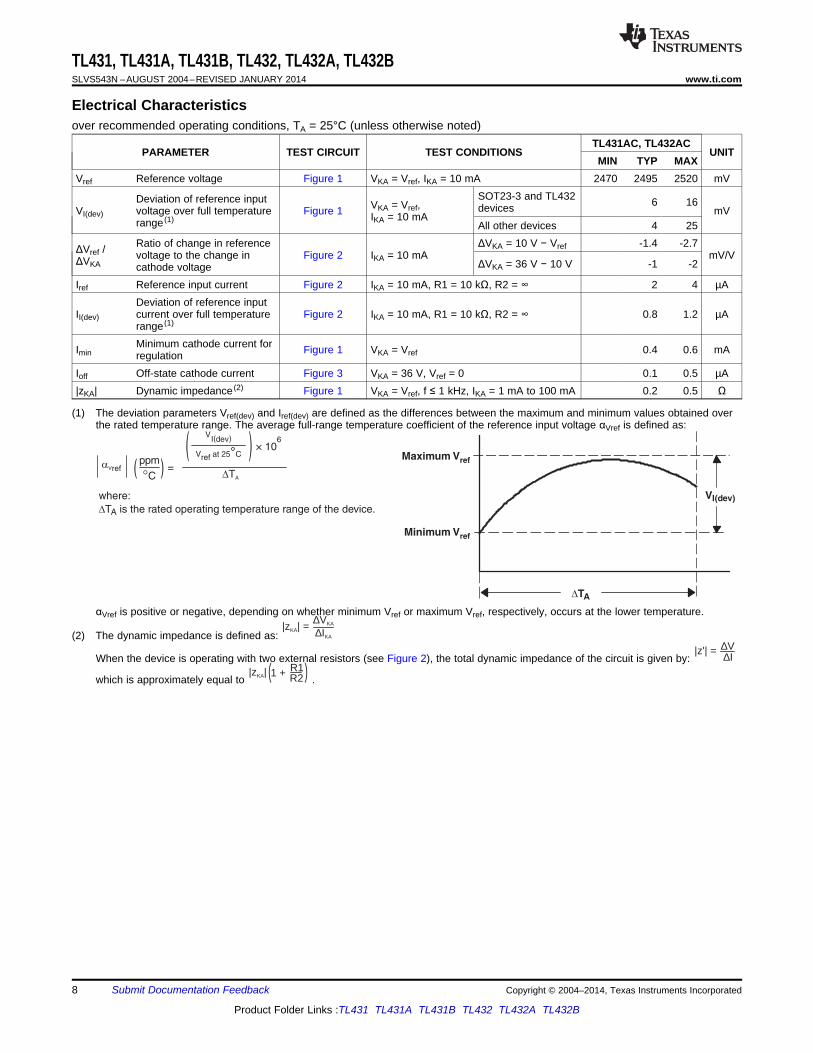
TL431AC, TL432ACPARAMETER TEST CIRCUIT TEST CONDITIONS UNIT
MIN TYP MAXVref Reference voltage Figure 1 VKA = Vref, IKA = 10 mA 2470 2495 2520 mV
SOT23-3 and TL432Deviation of reference input 6 16VKA = Vref, devicesVI(dev) voltage over full temperature Figure 1 mVIKA = 10 mArange (1) All other devices 4 25Ratio of change in reference ΔVKA = 10 V − Vref -1.4 -2.7ΔVref / voltage to the change in Figure 2 IKA = 10 mA mV/VΔVKA ΔVKA = 36 V − 10 V -1 -2cathode voltage
Iref Reference input current Figure 2 IKA = 10 mA, R1 = 10 kΩ, R2 = ∞ 2 4 µADeviation of reference input
II(dev) current over full temperature Figure 2 IKA = 10 mA, R1 = 10 kΩ, R2 = ∞ 0.8 1.2 µArange (1)
Minimum cathode current forImin Figure 1 VKA = Vref 0.4 0.6 mAregulationIoff Off-state cathode current Figure 3 VKA = 36 V, Vref = 0 0.1 0.5 µA|zKA| Dynamic impedance (2) Figure 1 VKA = Vref, f ≤ 1 kHz, IKA = 1 mA to 100 mA 0.2 0.5 Ω
(1) The deviation parameters Vref(dev) and Iref(dev) are defined as the differences between the maximum and minimum values obtained overthe rated temperature range. The average full-range temperature coefficient of the reference input voltage αVref is defined as:
αVref is positive or negative, depending on whether minimum Vref or maximum Vref, respectively, occurs at the lower temperature.
8 Submit Documentation Feedback Copyright © 2004–2014, Texas Instruments Incorporated
Product Folder Links :TL431 TL431A TL431B TL432 TL432A TL432B

R2R1|z |KA (1 + (
∆I∆V|z'| =
∆IKA
∆VKA|z | =KA(2) The dynamic impedance is defined as:
When the device is operating with two external resistors (see Figure 2), the total dynamic impedance of the circuit is given by:
which is approximately equal to .
TL431, TL431A, TL431B, TL432, TL432A, TL432Bwww.ti.com SLVS543N –AUGUST 2004–REVISED JANUARY 2014
Electrical Characteristicsover recommended operating conditions, TA = 25°C (unless otherwise noted)
TL431AI, TL432AIPARAMETER TEST CIRCUIT TEST CONDITIONS UNIT
MIN TYP MAXVref Reference voltage Figure 1 VKA = Vref, IKA = 10 mA 2470 2495 2520 mV
SOT23-3 and TL432Deviation of reference input 14 34VKA = Vref, devicesVI(dev) voltage over full temperature Figure 1 mVIKA = 10 mArange (1) All other devices 5 50Ratio of change in reference ΔVKA = 10 V − Vref -1.4 -2.7ΔVref / voltage to the change in Figure 2 IKA = 10 mA mV/VΔVKA ΔVKA = 36 V − 10 V -1 -2cathode voltage
Iref Reference input current Figure 2 IKA = 10 mA, R1 = 10 kΩ, R2 = ∞ 2 4 µADeviation of reference input
II(dev) current over full temperature Figure 2 IKA = 10 mA, R1 = 10 kΩ, R2 = ∞ 0.8 2.5 µArange (1)
Minimum cathode current forImin Figure 1 VKA = Vref 0.4 0.7 mAregulationIoff Off-state cathode current Figure 3 VKA = 36 V, Vref = 0 0.1 0.5 µA|zKA| Dynamic impedance (2) Figure 1 VKA = Vref, f ≤ 1 kHz, IKA = 1 mA to 100 mA 0.2 0.5 Ω
(1) The deviation parameters Vref(dev) and Iref(dev) are defined as the differences between the maximum and minimum values obtained overthe rated temperature range. The average full-range temperature coefficient of the reference input voltage αVref is defined as:
αVref is positive or negative, depending on whether minimum Vref or maximum Vref, respectively, occurs at the lower temperature.
Copyright © 2004–2014, Texas Instruments Incorporated Submit Documentation Feedback 9
Product Folder Links :TL431 TL431A TL431B TL432 TL432A TL432B
R2R1|z |KA (1 + (
∆I∆V|z'| =
∆IKA
∆VKA|z | =KA(2) The dynamic impedance is defined as:
When the device is operating with two external resistors (see Figure 2), the total dynamic impedance of the circuit is given by:
which is approximately equal to .
TL431, TL431A, TL431B, TL432, TL432A, TL432BSLVS543N –AUGUST 2004–REVISED JANUARY 2014 www.ti.com
Electrical Characteristicsover recommended operating conditions, TA = 25°C (unless otherwise noted)
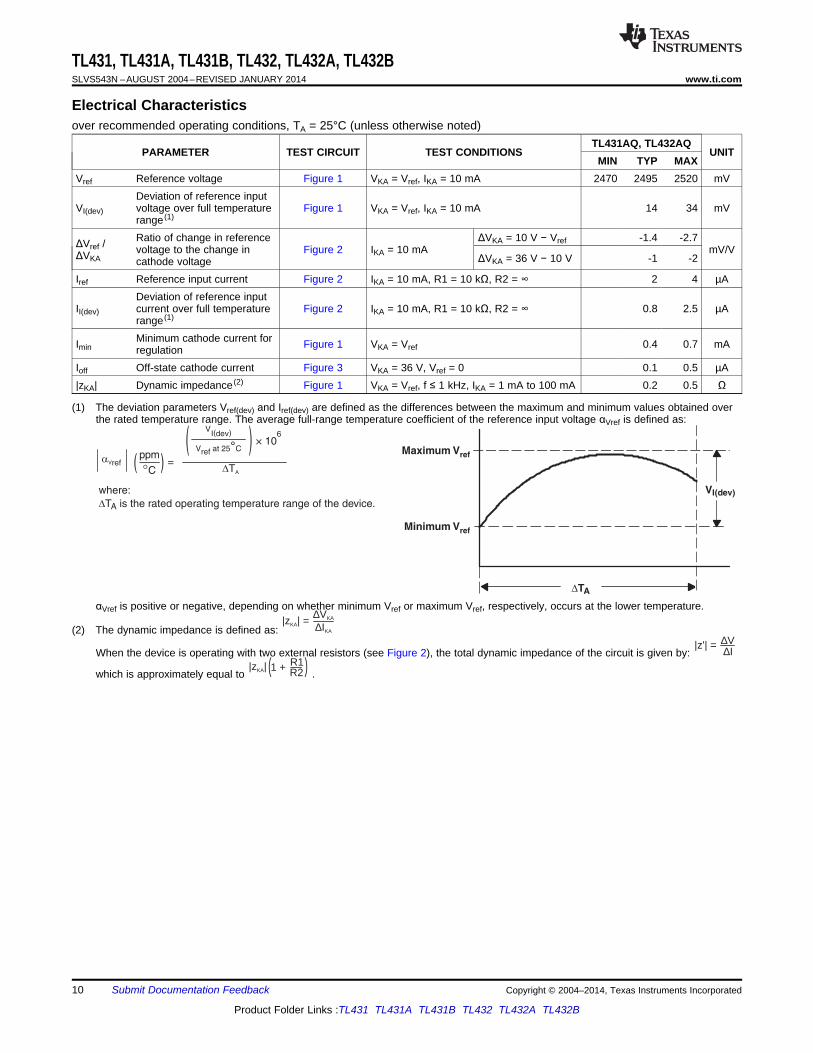
TL431AQ, TL432AQPARAMETER TEST CIRCUIT TEST CONDITIONS UNIT
MIN TYP MAXVref Reference voltage Figure 1 VKA = Vref, IKA = 10 mA 2470 2495 2520 mV
Deviation of reference inputVI(dev) voltage over full temperature Figure 1 VKA = Vref, IKA = 10 mA 14 34 mV
range (1)
Ratio of change in reference ΔVKA = 10 V − Vref -1.4 -2.7ΔVref / voltage to the change in Figure 2 IKA = 10 mA mV/VΔVKA ΔVKA = 36 V − 10 V -1 -2cathode voltageIref Reference input current Figure 2 IKA = 10 mA, R1 = 10 kΩ, R2 = ∞ 2 4 µA
Deviation of reference inputII(dev) current over full temperature Figure 2 IKA = 10 mA, R1 = 10 kΩ, R2 = ∞ 0.8 2.5 µA
range (1)
Minimum cathode current forImin Figure 1 VKA = Vref 0.4 0.7 mAregulationIoff Off-state cathode current Figure 3 VKA = 36 V, Vref = 0 0.1 0.5 µA|zKA| Dynamic impedance (2) Figure 1 VKA = Vref, f ≤ 1 kHz, IKA = 1 mA to 100 mA 0.2 0.5 Ω
(1) The deviation parameters Vref(dev) and Iref(dev) are defined as the differences between the maximum and minimum values obtained overthe rated temperature range. The average full-range temperature coefficient of the reference input voltage αVref is defined as:
αVref is positive or negative, depending on whether minimum Vref or maximum Vref, respectively, occurs at the lower temperature.
10 Submit Documentation Feedback Copyright © 2004–2014, Texas Instruments Incorporated
Product Folder Links :TL431 TL431A TL431B TL432 TL432A TL432B

R2R1|z |KA (1 + (
∆I∆V|z'| =
∆IKA
∆VKA|z | =KA(2) The dynamic impedance is defined as:
When the device is operating with two external resistors (see Figure 2), the total dynamic impedance of the circuit is given by:
which is approximately equal to .
TL431, TL431A, TL431B, TL432, TL432A, TL432Bwww.ti.com SLVS543N –AUGUST 2004–REVISED JANUARY 2014
Electrical Characteristicsover recommended operating conditions, TA = 25°C (unless otherwise noted)
TL431BC, TL432BCPARAMETER TEST CIRCUIT TEST CONDITIONS UNIT
MIN TYP MAXVref Reference voltage Figure 1 VKA = Vref, IKA = 10 mA 2483 2495 2507 mV
Deviation of reference inputVI(dev) voltage over full temperature Figure 1 VKA = Vref, IKA = 10 mA 6 16 mV
range (1)
Ratio of change in reference ΔVKA = 10 V − Vref -1.4 -2.7ΔVref / voltage to the change in Figure 2 IKA = 10 mA mV/VΔVKA ΔVKA = 36 V − 10 V -1 -2cathode voltageIref Reference input current Figure 2 IKA = 10 mA, R1 = 10 kΩ, R2 = ∞ 2 4 µA
Deviation of reference inputII(dev) current over full temperature Figure 2 IKA = 10 mA, R1 = 10 kΩ, R2 = ∞ 0.8 1.2 µA
range (1)
Minimum cathode current forImin Figure 1 VKA = Vref 0.4 0.6 mAregulationIoff Off-state cathode current Figure 3 VKA = 36 V, Vref = 0 0.1 0.5 µA|zKA| Dynamic impedance (2) Figure 1 VKA = Vref, f ≤ 1 kHz, IKA = 1 mA to 100 mA 0.2 0.5 Ω
(1) The deviation parameters Vref(dev) and Iref(dev) are defined as the differences between the maximum and minimum values obtained overthe rated temperature range. The average full-range temperature coefficient of the reference input voltage αVref is defined as:
αVref is positive or negative, depending on whether minimum Vref or maximum Vref, respectively, occurs at the lower temperature.
Copyright © 2004–2014, Texas Instruments Incorporated Submit Documentation Feedback 11
Product Folder Links :TL431 TL431A TL431B TL432 TL432A TL432B

R2R1|z |KA (1 + (
∆I∆V|z'| =
∆IKA
∆VKA|z | =KA(2) The dynamic impedance is defined as:
When the device is operating with two external resistors (see Figure 2), the total dynamic impedance of the circuit is given by:
which is approximately equal to .
TL431, TL431A, TL431B, TL432, TL432A, TL432BSLVS543N –AUGUST 2004–REVISED JANUARY 2014 www.ti.com
Electrical Characteristicsover recommended operating conditions, TA = 25°C (unless otherwise noted)
TL431BI, TL432BIPARAMETER TEST CIRCUIT TEST CONDITIONS UNIT
MIN TYP MAXVref Reference voltage Figure 1 VKA = Vref, IKA = 10 mA 2483 2495 2507 mV
Deviation of reference inputVI(dev) voltage over full temperature Figure 1 VKA = Vref, IKA = 10 mA 14 34 mV
range (1)
Ratio of change in reference ΔVKA = 10 V − Vref -1.4 -2.7ΔVref / voltage to the change in Figure 2 IKA = 10 mA mV/VΔVKA ΔVKA = 36 V − 10 V -1 -2cathode voltageIref Reference input current Figure 2 IKA = 10 mA, R1 = 10 kΩ, R2 = ∞ 2 4 µA
Deviation of reference inputII(dev) current over full temperature Figure 2 IKA = 10 mA, R1 = 10 kΩ, R2 = ∞ 0.8 2.5 µA
range (1)
Minimum cathode current forImin Figure 1 VKA = Vref 0.4 0.7 mAregulationIoff Off-state cathode current Figure 3 VKA = 36 V, Vref = 0 0.1 0.5 µA|zKA| Dynamic impedance (2) Figure 1 VKA = Vref, f ≤ 1 kHz, IKA = 1 mA to 100 mA 0.2 0.5 Ω
(1) The deviation parameters Vref(dev) and Iref(dev) are defined as the differences between the maximum and minimum values obtained overthe rated temperature range. The average full-range temperature coefficient of the reference input voltage αVref is defined as:
αVref is positive or negative, depending on whether minimum Vref or maximum Vref, respectively, occurs at the lower temperature.
12 Submit Documentation Feedback Copyright © 2004–2014, Texas Instruments Incorporated
Product Folder Links :TL431 TL431A TL431B TL432 TL432A TL432B

R2R1|z |KA (1 + (
∆I∆V|z'| =
∆IKA
∆VKA|z | =KA(2) The dynamic impedance is defined as:
When the device is operating with two external resistors (see Figure 2), the total dynamic impedance of the circuit is given by:
which is approximately equal to .
TL431, TL431A, TL431B, TL432, TL432A, TL432Bwww.ti.com SLVS543N –AUGUST 2004–REVISED JANUARY 2014
Electrical Characteristicsover recommended operating conditions, TA = 25°C (unless otherwise noted)
TL431BQ, TL432BQPARAMETER TEST CIRCUIT TEST CONDITIONS UNIT
MIN TYP MAXVref Reference voltage Figure 1 VKA = Vref, IKA = 10 mA 2483 2495 2507 mV
Deviation of reference inputVI(dev) voltage over full temperature Figure 1 VKA = Vref, IKA = 10 mA 14 34 mV
range (1)
Ratio of change in reference ΔVKA = 10 V − Vref -1.4 -2.7ΔVref / voltage to the change in Figure 2 IKA = 10 mA mV/VΔVKA ΔVKA = 36 V − 10 V -1 -2cathode voltageIref Reference input current Figure 2 IKA = 10 mA, R1 = 10 kΩ, R2 = ∞ 2 4 µA
Deviation of reference inputII(dev) current over full temperature Figure 2 IKA = 10 mA, R1 = 10 kΩ, R2 = ∞ 0.8 2.5 µA
range (1)
Minimum cathode current forImin Figure 1 VKA = Vref 0.4 0.7 mAregulationIoff Off-state cathode current Figure 3 VKA = 36 V, Vref = 0 0.1 0.5 µA|zKA| Dynamic impedance (2) Figure 1 VKA = Vref, f ≤ 1 kHz, IKA = 1 mA to 100 mA 0.2 0.5 Ω
(1) The deviation parameters Vref(dev) and Iref(dev) are defined as the differences between the maximum and minimum values obtained overthe rated temperature range. The average full-range temperature coefficient of the reference input voltage αVref is defined as:
αVref is positive or negative, depending on whether minimum Vref or maximum Vref, respectively, occurs at the lower temperature.
Copyright © 2004–2014, Texas Instruments Incorporated Submit Documentation Feedback 13
Product Folder Links :TL431 TL431A TL431B TL432 TL432A TL432B
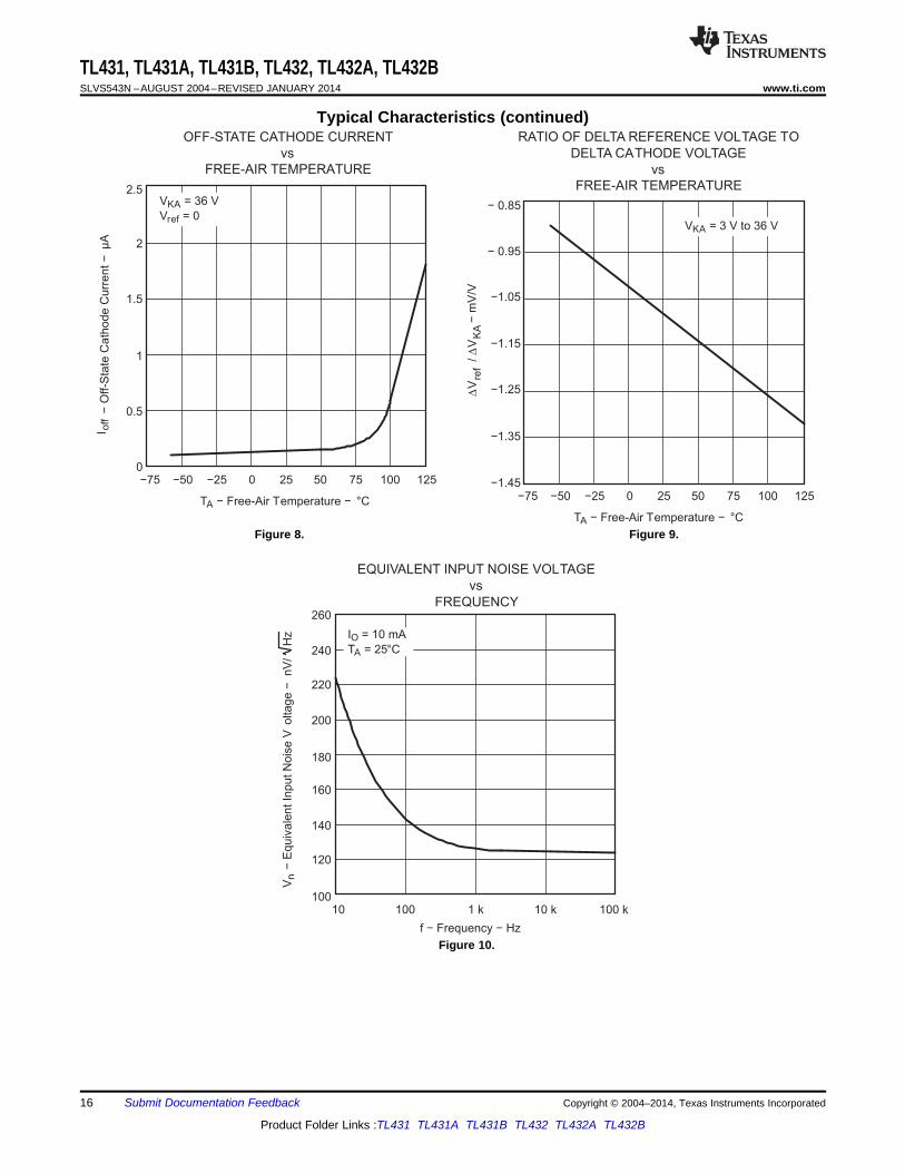
Ioff
VKAInput
Iref
IKA
VKAInput
Vref
R1
R2KA ref ref
R1V = V 1 + + I × R1
R2
æ öç ÷è ø
Vref
Input VKA
IKA
TL431, TL431A, TL431B, TL432, TL432A, TL432BSLVS543N –AUGUST 2004–REVISED JANUARY 2014 www.ti.com
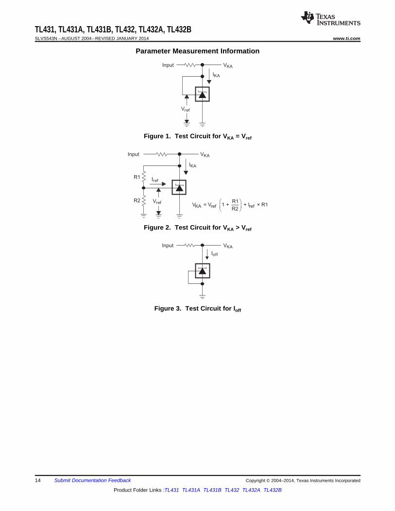
Parameter Measurement Information
Figure 1. Test Circuit for VKA = Vref
Figure 2. Test Circuit for VKA > Vref
Figure 3. Test Circuit for Ioff
14 Submit Documentation Feedback Copyright © 2004–2014, Texas Instruments Incorporated
Product Folder Links :TL431 TL431A TL431B TL432 TL432A TL432B
25
0
−50
−75
−100
125
−25
−2 −1 0 1
75
50
100
CATHODE CURRENT
vs
CATHODE VOLTAGE150
2 3
VKA − Cathode Voltage − V
VKA = Vref
TA = 25°C
−C
ath
ode C
urr
ent
−m
AI K
A
400
200
0
−200−1 0 1
600
CATHODE CURRENT
vs
CATHODE VOLTAGE800
2 3
VKA = Vref
TA = 25°C
VKA − Cathode Voltage − V
Imin
−C
ath
ode C
urr
ent
−I K
AA
µ
2500
2480
2420
2400−75 −50 −25 0 25 50 75
2540
2580
REFERENCE VOLTAGE
vs
FREE-AIR TEMPERATURE2600
100 125
2460
2560
2520
2440
TA − Free-Air Temperature − °C
Vref = 2495 mV
Vref = 2440 mV
VKA = Vref
IKA = 10 mA
Vref = 2550 mV
−R
efe
rence V
oltage
−m
VV
ref
3
2
1
0−75 −25 0 50
4
REFERENCE CURRENT
vs
FREE-AIR TEMPERATURE
5
100 125−50 25 75
TA − Free-Air Temperature − °C
R1 = 10 kΩ
R2 = ∞
IKA = 10 mA
−R
efe
rence C
urr
ent
−re
fI
µA
TL431, TL431A, TL431B, TL432, TL432A, TL432Bwww.ti.com SLVS543N –AUGUST 2004–REVISED JANUARY 2014
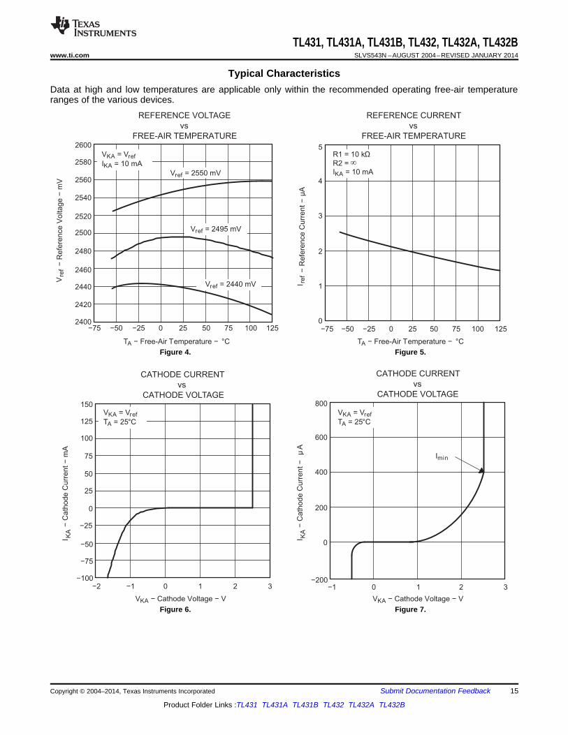
Typical CharacteristicsData at high and low temperatures are applicable only within the recommended operating free-air temperatureranges of the various devices.
Figure 4. Figure 5.
Figure 6. Figure 7.
Copyright © 2004–2014, Texas Instruments Incorporated Submit Documentation Feedback 15
Product Folder Links :TL431 TL431A TL431B TL432 TL432A TL432B
180
140
120
10010 100 1 k
220
240
f − Frequency − Hz
EQUIVALENT INPUT NOISE VOLTAGE
vs
FREQUENCY260
10 k 100 k
200
160
−E
quiv
ale
nt In
put N
ois
e V
oltage
−nV
/H
zV
n
IO = 10 mA
TA = 25°C
−1.15
−1.25
−1.35
−1.45
−1.05
− 0.95
RATIO OF DELTA REFERENCE VOLTAGE TO
DELTA CATHODE VOLTAGE
vs
FREE-AIR TEMPERATURE
− 0.85
TA − Free-Air Temperature − °C
−75 −25 0 50 100 125−50 25 75
VKA = 3 V to 36 V
−m
V/V
∆V
ref
∆V
KA
/
1.5
1
0.5
0−75 −25 0 50
−O
ff-S
tate
Cath
ode C
urr
ent
−
2
OFF-STATE CATHODE CURRENT
vs
FREE-AIR TEMPERATURE
2.5
100 125−50 25 75
I off
µA
TA − Free-Air Temperature − °C
VKA = 36 V
Vref = 0
TL431, TL431A, TL431B, TL432, TL432A, TL432BSLVS543N –AUGUST 2004–REVISED JANUARY 2014 www.ti.com
Typical Characteristics (continued)
Figure 8. Figure 9.
Figure 10.
16 Submit Documentation Feedback Copyright © 2004–2014, Texas Instruments Incorporated
Product Folder Links :TL431 TL431A TL431B TL432 TL432A TL432B
19.1 V
VCC
TLE2027
TLE2027
AV = 10 V/mV
VEE
0.1 µF
160 kΩ
820 Ω
(DUT)TL431
16 Ω
910 Ω
2000 µF
1 kΩ
VEE
VCC1 µF
16 kΩ 16 kΩ
1 µF 33 kΩ
33 kΩ
AV = 2 V/V
22 µF
500 µF
To
Oscilloscope
−1
−2
−4
−5
−6
3
−3
0 1 2 3 4 5 6
1
0
2
EQUIVALENT INPUT NOISE VOLTAGE
OVER A 10-S PERIOD
4
7 8 9 10
5
6
t − Time − s
f = 0.1 to 10 Hz
IKA = 10 mA
TA = 25°C
−E
quiv
ale
nt In
put N
ois
e V
oltage
−µ
VV
n
+
−+
−
TL431, TL431A, TL431B, TL432, TL432A, TL432Bwww.ti.com SLVS543N –AUGUST 2004–REVISED JANUARY 2014
Typical Characteristics (continued)
Figure 11.
Copyright © 2004–2014, Texas Instruments Incorporated Submit Documentation Feedback 17
Product Folder Links :TL431 TL431A TL431B TL432 TL432A TL432B
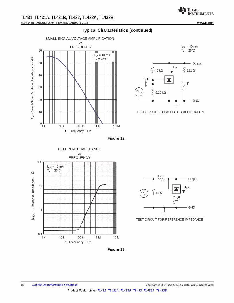
1 kΩ
50 Ω
GND
Output
IKA
0.11 k 10 k 100 k 1 M 10 M
1
f − Frequency − Hz
REFERENCE IMPEDANCE
vs
FREQUENCY
10
100
IKA = 10 mA
TA = 25°C
TEST CIRCUIT FOR REFERENCE IMPEDANCE
−R
efe
rence Im
pedance
−K
A|z
|Ω
+
−
1 k 10 k 100 k 1 M 10 M0
10
20
30
50
60
40
SMALL-SIGNAL VOLTAGE AMPLIFICATION
vs
FREQUENCY
9 µF
GND
Output
232 Ω
8.25 kΩ
IKA15 kΩ
f − Frequency − Hz
TEST CIRCUIT FOR VOLTAGE AMPLIFICATION
IKA = 10 mA
TA = 25°C
−S
mall-
Sig
nal V
oltage
Am
plif
ication
−dB
AV
+
−
IKA = 10 mA
TA = 25°C
TL431, TL431A, TL431B, TL432, TL432A, TL432BSLVS543N –AUGUST 2004–REVISED JANUARY 2014 www.ti.com
Typical Characteristics (continued)
Figure 12.
Figure 13.
18 Submit Documentation Feedback Copyright © 2004–2014, Texas Instruments Incorporated
Product Folder Links :TL431 TL431A TL431B TL432 TL432A TL432B

150 Ω
IKA
R1 = 10 kΩ
R2
CL
VBATT
IKA
CLVBATT
150 Ω
TEST CIRCUIT FOR CURVE A
TEST CIRCUIT FOR CURVES B, C, AND D
50
40
10
00.001 0.01 0.1 1
70
90
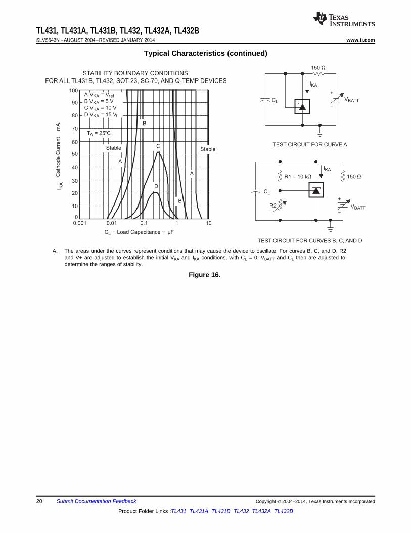
STABILITY BOUNDARY CONDITIONS
FOR ALL TL431 AND TL431A DEVICES
(EXCEPT FOR SOT23-3, SC-70, AND Q-TEMP DEVICES)
100
10
30
80
60
20
TA = 25°C
B
Stable
Stable
A VKA = Vref
B VKA = 5 V
C VKA = 10 V
D VKA = 15 Vf
CL − Load Capacitance − µF
A
C
D
−C
ath
ode C
urr
ent
−m
AI K
A
+
−
+
−
3
2
1
0−1 0 1 2 3 4
Input and O
utp
ut V
oltage
−V
4
5
PULSE RESPONSE
6
5 6 7
Input
Output
TA = 25°C
220 Ω
50 Ω
GND
Output
Pulse
Generator
f = 100 kHz
TEST CIRCUIT FOR PULSE RESPONSE
t − Time − µs
TL431, TL431A, TL431B, TL432, TL432A, TL432Bwww.ti.com SLVS543N –AUGUST 2004–REVISED JANUARY 2014
Typical Characteristics (continued)
Figure 14.
A. The areas under the curves represent conditions that may cause the device to oscillate. For curves B, C, and D, R2and V+ are adjusted to establish the initial VKA and IKA conditions, with CL = 0. VBATT and CL then are adjusted todetermine the ranges of stability.
Figure 15.
Copyright © 2004–2014, Texas Instruments Incorporated Submit Documentation Feedback 19
Product Folder Links :TL431 TL431A TL431B TL432 TL432A TL432B
50
40
10
00.001 0.01 0.1 1
70
90
STABILITY BOUNDARY CONDITIONS
FOR ALL TL431B, TL432, SOT-23, SC-70, AND Q-TEMP DEVICES
100
10
30
80
60
20
Stable
A VKA = Vref
B VKA = 5 V
C VKA = 10 V
D VKA = 15 Vf
CL − Load Capacitance − µF
A
C
D
150 Ω
IKA
R1 = 10 kΩ
R2
CL
VBATT
IKA
CLVBATT
150 Ω
TEST CIRCUIT FOR CURVE A
TEST CIRCUIT FOR CURVES B, C, AND D
−C
ath
ode C
urr
ent
−m
AI K
A
+
−
+
−
B
A
TA = 25°C
Stable
B
TL431, TL431A, TL431B, TL432, TL432A, TL432BSLVS543N –AUGUST 2004–REVISED JANUARY 2014 www.ti.com
Typical Characteristics (continued)
A. The areas under the curves represent conditions that may cause the device to oscillate. For curves B, C, and D, R2and V+ are adjusted to establish the initial VKA and IKA conditions, with CL = 0. VBATT and CL then are adjusted todetermine the ranges of stability.
Figure 16.
20 Submit Documentation Feedback Copyright © 2004–2014, Texas Instruments Incorporated
Product Folder Links :TL431 TL431A TL431B TL432 TL432A TL432B
R
(see Note A)
VOTL431
VI(BATT)
2N222
2N222
4.7 kΩ
R1
0.1%R2
0.1%
0.01 µF
30 Ω
O refR1
V = 1 + VR2
æ öç ÷è ø
VOTL431
VI(BATT)
VIT ≈ 2.5 V
GND
InputVon ≈2 V
Voff ≈VI(BATT)
R1
0.1%
R2
0.1%
R
(see Note A)
Vref
VO
TL431
VI(BATT)
RETURN
O refR1
V = 1 + VR2
æ öç ÷è ø
TL431, TL431A, TL431B, TL432, TL432A, TL432Bwww.ti.com SLVS543N –AUGUST 2004–REVISED JANUARY 2014
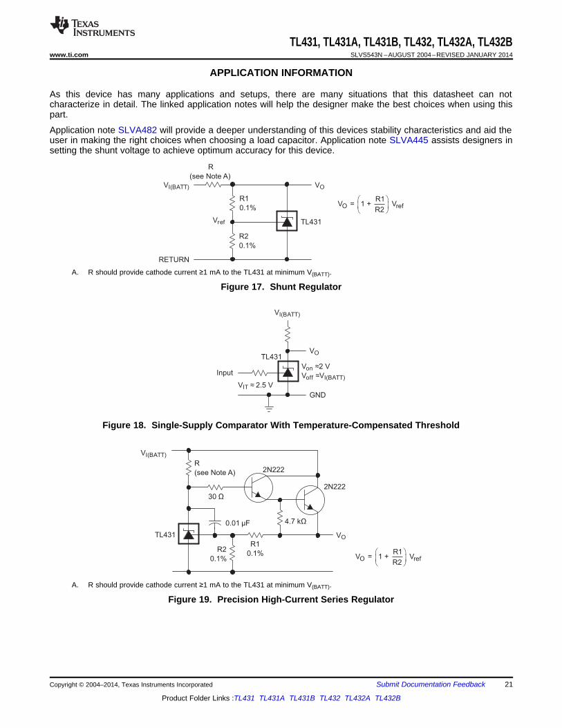
APPLICATION INFORMATION
As this device has many applications and setups, there are many situations that this datasheet can notcharacterize in detail. The linked application notes will help the designer make the best choices when using thispart.
Application note SLVA482 will provide a deeper understanding of this devices stability characteristics and aid theuser in making the right choices when choosing a load capacitor. Application note SLVA445 assists designers insetting the shunt voltage to achieve optimum accuracy for this device.
A. R should provide cathode current ≥1 mA to the TL431 at minimum V(BATT).
Figure 17. Shunt Regulator
Figure 18. Single-Supply Comparator With Temperature-Compensated Threshold
A. R should provide cathode current ≥1 mA to the TL431 at minimum V(BATT).
Figure 19. Precision High-Current Series Regulator
Copyright © 2004–2014, Texas Instruments Incorporated Submit Documentation Feedback 21
Product Folder Links :TL431 TL431A TL431B TL432 TL432A TL432B
VO ≈5 V, 1.5 A
TL431
VI(BATT) LM317IN OUT
Adjust243 Ω
0.1%
243 Ω
0.1%
8.2 kΩ
VO
TL431
VI(BATT)
R1
R2
C
(see Note A)
VO
TL431
VI(BATT)
R1
R2
VO
1 R1R2
Vref= +( (
VO
TL431
VI(BATT)
uA7805
INOUT
Common R1
R2
VO
1 R1R2
Vref
Minimum VO
Vref 5 V
= +
= +
( (
TL431, TL431A, TL431B, TL432, TL432A, TL432BSLVS543N –AUGUST 2004–REVISED JANUARY 2014 www.ti.com
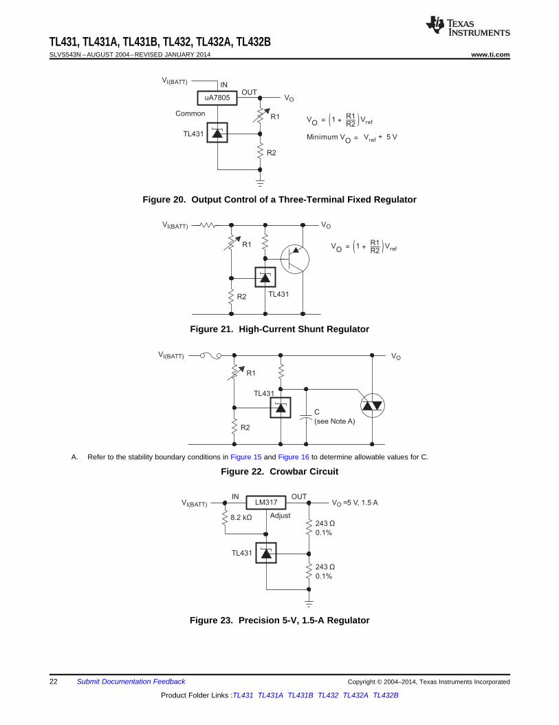
Figure 20. Output Control of a Three-Terminal Fixed Regulator
Figure 21. High-Current Shunt Regulator
A. Refer to the stability boundary conditions in Figure 15 and Figure 16 to determine allowable values for C.
Figure 22. Crowbar Circuit
Figure 23. Precision 5-V, 1.5-A Regulator
22 Submit Documentation Feedback Copyright © 2004–2014, Texas Instruments Incorporated
Product Folder Links :TL431 TL431A TL431B TL432 TL432A TL432B

TL431
VI(BATT)
R3
(see Note A)
R1AR4
(see Note A)
R2BR2A
R1B
Low Limit = 1 + R1BR2B
Vref
High Limit = 1 + R1AR2A
Vref
LED on When Low Limit < VI(BATT) < High Limit
TL431
12 V
VCC
5 V
6.8 kΩ
10 kΩ
10 kΩ
0.1%
10 kΩ
0.1%
X
Not
Used
Feedback
TL598+
−
VO ≈5 V
TL431
VI(BATT)
27.4 kΩ
0.1%
Rb
(see Note A)
27.4 kΩ
0.1%
TL431, TL431A, TL431B, TL432, TL432A, TL432Bwww.ti.com SLVS543N –AUGUST 2004–REVISED JANUARY 2014
A. Rb should provide cathode current ≥1 mA to the TL431.
Figure 24. Efficient 5-V Precision Regulator
Figure 25. PWM Converter With Reference
A. Select R3 and R4 to provide the desired LED intensity and cathode current ≥1 mA to the TL431 at the availableVI(BATT).
Figure 26. Voltage Monitor
Copyright © 2004–2014, Texas Instruments Incorporated Submit Documentation Feedback 23
Product Folder Links :TL431 TL431A TL431B TL432 TL432A TL432B
TL431
RS
0.1%
IO
VI(BATT)
IO
Vref
RS=
TL431
IORCL
0.1%
R1
VI(BATT) Iout
Vref
RCL
IKA
R1VI(BATT)
IO
hFE
IKA
+
+
=
=
TL431
650 Ω
2 kΩ
COn
Off
R
12 V
nref
12 VDelay = R × C × I
12 V – V
æ öç ÷ç ÷è ø
TL431, TL431A, TL431B, TL432, TL432A, TL432BSLVS543N –AUGUST 2004–REVISED JANUARY 2014 www.ti.com
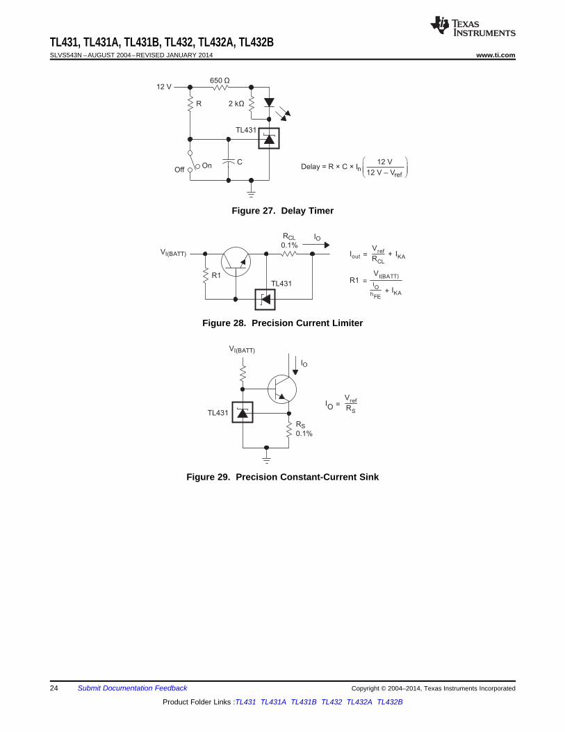
Figure 27. Delay Timer
Figure 28. Precision Current Limiter
Figure 29. Precision Constant-Current Sink
24 Submit Documentation Feedback Copyright © 2004–2014, Texas Instruments Incorporated
Product Folder Links :TL431 TL431A TL431B TL432 TL432A TL432B
TL431, TL431A, TL431B, TL432, TL432A, TL432Bwww.ti.com SLVS543N –AUGUST 2004–REVISED JANUARY 2014
REVISION HISTORY
Changes from Revision K (June 2010) to Revision L Page
• Deleted TA values under TEST CONDITIONS for VI(dev) and II(dev) PARAMTERS in the ELECTRICALCHRACTERISTICS table. ..................................................................................................................................................... 5
Changes from Revision L (Feb 2011) to Revision M Page
• Updated orderable part number in ordering information table. ............................................................................................. 3
Changes from Revision M (July 2012) to Revision N Page
• Updated document formatting .............................................................................................................................................. 1• Removed ordering information table. .................................................................................................................................... 3• Added Application Note Links ............................................................................................................................................. 21
Copyright © 2004–2014, Texas Instruments Incorporated Submit Documentation Feedback 25
Product Folder Links :TL431 TL431A TL431B TL432 TL432A TL432B
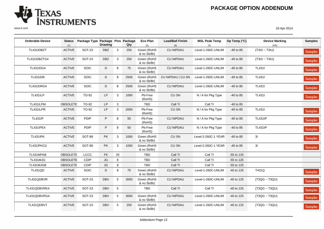
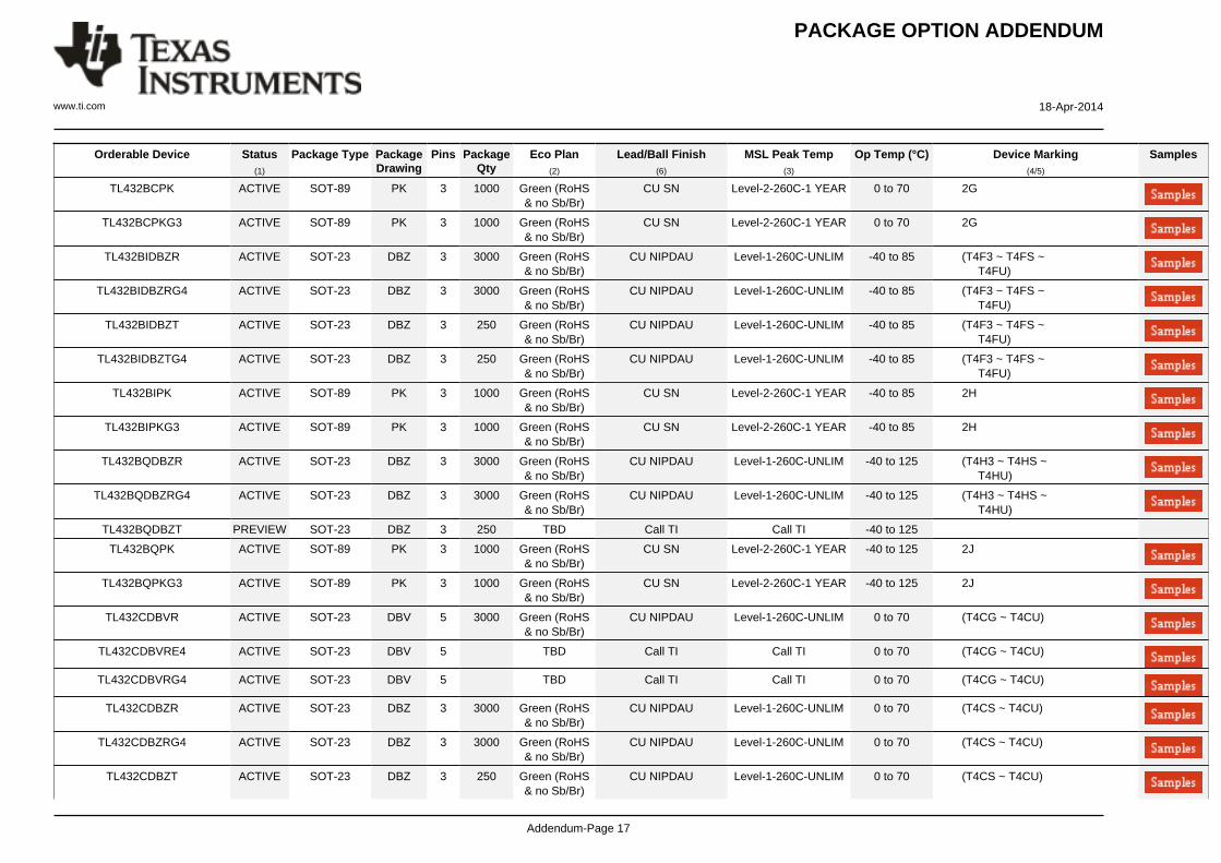
PACKAGE OPTION ADDENDUM
www.ti.com 18-Apr-2014
Addendum-Page 1
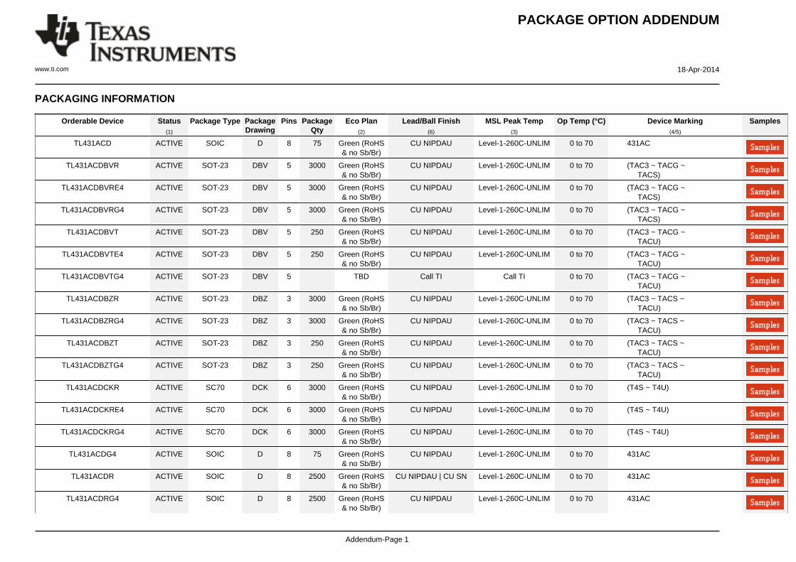
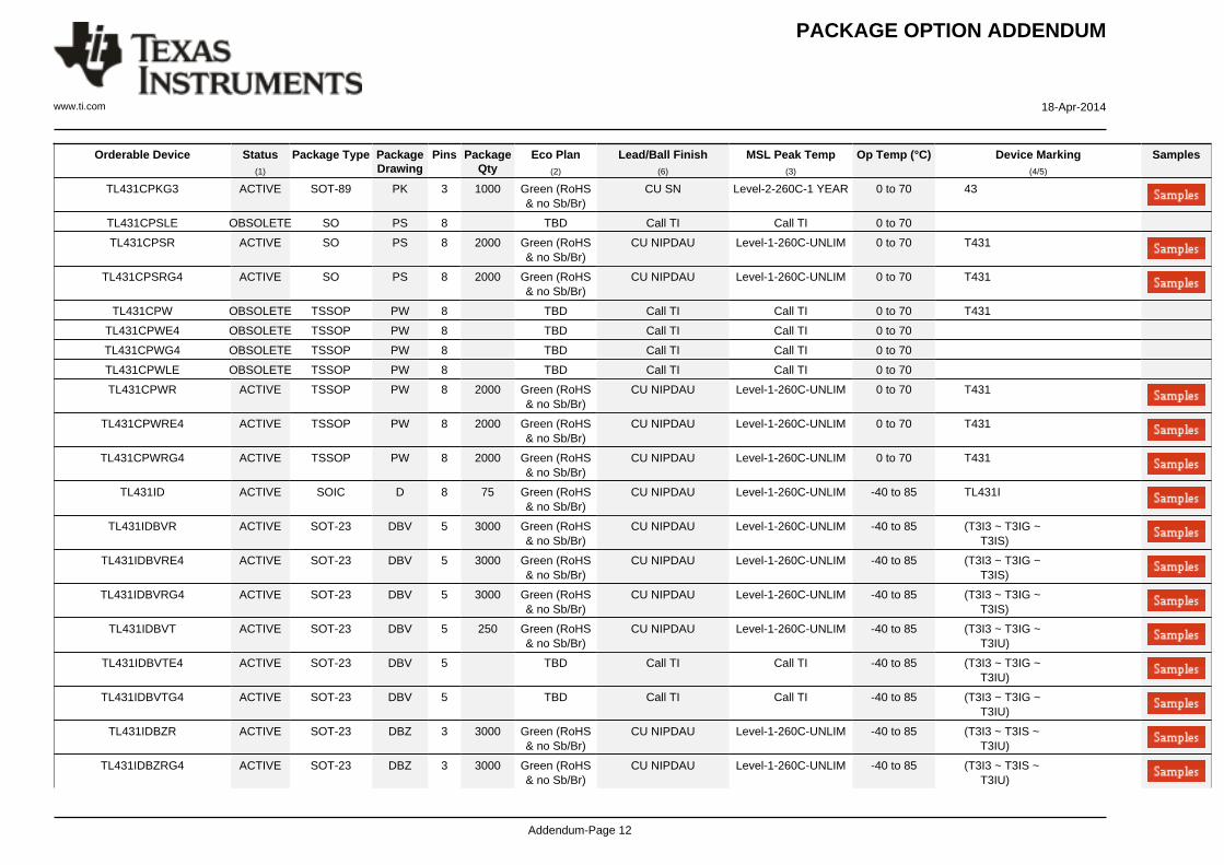
PACKAGING INFORMATION
Orderable Device Status(1)
Package Type PackageDrawing
Pins PackageQty
Eco Plan(2)
Lead/Ball Finish(6)
MSL Peak Temp(3)
Op Temp (°C) Device Marking(4/5)
Samples
TL431ACD ACTIVE SOIC D 8 75 Green (RoHS& no Sb/Br)
CU NIPDAU Level-1-260C-UNLIM 0 to 70 431AC
TL431ACDBVR ACTIVE SOT-23 DBV 5 3000 Green (RoHS& no Sb/Br)
CU NIPDAU Level-1-260C-UNLIM 0 to 70 (TAC3 ~ TACG ~ TACS)
TL431ACDBVRE4 ACTIVE SOT-23 DBV 5 3000 Green (RoHS& no Sb/Br)
CU NIPDAU Level-1-260C-UNLIM 0 to 70 (TAC3 ~ TACG ~ TACS)
TL431ACDBVRG4 ACTIVE SOT-23 DBV 5 3000 Green (RoHS& no Sb/Br)
CU NIPDAU Level-1-260C-UNLIM 0 to 70 (TAC3 ~ TACG ~ TACS)
TL431ACDBVT ACTIVE SOT-23 DBV 5 250 Green (RoHS& no Sb/Br)
CU NIPDAU Level-1-260C-UNLIM 0 to 70 (TAC3 ~ TACG ~ TACU)
TL431ACDBVTE4 ACTIVE SOT-23 DBV 5 250 Green (RoHS& no Sb/Br)
CU NIPDAU Level-1-260C-UNLIM 0 to 70 (TAC3 ~ TACG ~ TACU)
TL431ACDBVTG4 ACTIVE SOT-23 DBV 5 TBD Call TI Call TI 0 to 70 (TAC3 ~ TACG ~ TACU)
TL431ACDBZR ACTIVE SOT-23 DBZ 3 3000 Green (RoHS& no Sb/Br)
CU NIPDAU Level-1-260C-UNLIM 0 to 70 (TAC3 ~ TACS ~ TACU)
TL431ACDBZRG4 ACTIVE SOT-23 DBZ 3 3000 Green (RoHS& no Sb/Br)
CU NIPDAU Level-1-260C-UNLIM 0 to 70 (TAC3 ~ TACS ~ TACU)
TL431ACDBZT ACTIVE SOT-23 DBZ 3 250 Green (RoHS& no Sb/Br)
CU NIPDAU Level-1-260C-UNLIM 0 to 70 (TAC3 ~ TACS ~ TACU)
TL431ACDBZTG4 ACTIVE SOT-23 DBZ 3 250 Green (RoHS& no Sb/Br)
CU NIPDAU Level-1-260C-UNLIM 0 to 70 (TAC3 ~ TACS ~ TACU)
TL431ACDCKR ACTIVE SC70 DCK 6 3000 Green (RoHS& no Sb/Br)
CU NIPDAU Level-1-260C-UNLIM 0 to 70 (T4S ~ T4U)
TL431ACDCKRE4 ACTIVE SC70 DCK 6 3000 Green (RoHS& no Sb/Br)
CU NIPDAU Level-1-260C-UNLIM 0 to 70 (T4S ~ T4U)
TL431ACDCKRG4 ACTIVE SC70 DCK 6 3000 Green (RoHS& no Sb/Br)
CU NIPDAU Level-1-260C-UNLIM 0 to 70 (T4S ~ T4U)
TL431ACDG4 ACTIVE SOIC D 8 75 Green (RoHS& no Sb/Br)
CU NIPDAU Level-1-260C-UNLIM 0 to 70 431AC
TL431ACDR ACTIVE SOIC D 8 2500 Green (RoHS& no Sb/Br)
CU NIPDAU | CU SN Level-1-260C-UNLIM 0 to 70 431AC
TL431ACDRG4 ACTIVE SOIC D 8 2500 Green (RoHS& no Sb/Br)
CU NIPDAU Level-1-260C-UNLIM 0 to 70 431AC
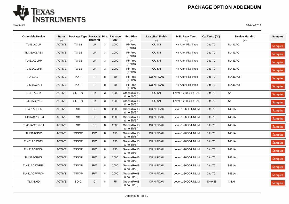
PACKAGE OPTION ADDENDUM
www.ti.com 18-Apr-2014
Addendum-Page 2
Orderable Device Status(1)
Package Type PackageDrawing
Pins PackageQty
Eco Plan(2)
Lead/Ball Finish(6)
MSL Peak Temp(3)
Op Temp (°C) Device Marking(4/5)
Samples
TL431ACLP ACTIVE TO-92 LP 3 1000 Pb-Free(RoHS)
CU SN N / A for Pkg Type 0 to 70 TL431AC
TL431ACLPE3 ACTIVE TO-92 LP 3 1000 Pb-Free(RoHS)
CU SN N / A for Pkg Type 0 to 70 TL431AC
TL431ACLPM ACTIVE TO-92 LP 3 2000 Pb-Free(RoHS)
CU SN N / A for Pkg Type 0 to 70 TL431AC
TL431ACLPR ACTIVE TO-92 LP 3 2000 Pb-Free(RoHS)
CU SN N / A for Pkg Type 0 to 70 TL431AC
TL431ACP ACTIVE PDIP P 8 50 Pb-Free(RoHS)
CU NIPDAU N / A for Pkg Type 0 to 70 TL431ACP
TL431ACPE4 ACTIVE PDIP P 8 50 Pb-Free(RoHS)
CU NIPDAU N / A for Pkg Type 0 to 70 TL431ACP
TL431ACPK ACTIVE SOT-89 PK 3 1000 Green (RoHS& no Sb/Br)
CU SN Level-2-260C-1 YEAR 0 to 70 4A
TL431ACPKG3 ACTIVE SOT-89 PK 3 1000 Green (RoHS& no Sb/Br)
CU SN Level-2-260C-1 YEAR 0 to 70 4A
TL431ACPSR ACTIVE SO PS 8 2000 Green (RoHS& no Sb/Br)
CU NIPDAU Level-1-260C-UNLIM 0 to 70 T431A
TL431ACPSRE4 ACTIVE SO PS 8 2000 Green (RoHS& no Sb/Br)
CU NIPDAU Level-1-260C-UNLIM 0 to 70 T431A
TL431ACPSRG4 ACTIVE SO PS 8 2000 Green (RoHS& no Sb/Br)
CU NIPDAU Level-1-260C-UNLIM 0 to 70 T431A
TL431ACPW ACTIVE TSSOP PW 8 150 Green (RoHS& no Sb/Br)
CU NIPDAU Level-1-260C-UNLIM 0 to 70 T431A
TL431ACPWE4 ACTIVE TSSOP PW 8 150 Green (RoHS& no Sb/Br)
CU NIPDAU Level-1-260C-UNLIM 0 to 70 T431A
TL431ACPWG4 ACTIVE TSSOP PW 8 150 Green (RoHS& no Sb/Br)
CU NIPDAU Level-1-260C-UNLIM 0 to 70 T431A
TL431ACPWR ACTIVE TSSOP PW 8 2000 Green (RoHS& no Sb/Br)
CU NIPDAU Level-1-260C-UNLIM 0 to 70 T431A
TL431ACPWRE4 ACTIVE TSSOP PW 8 2000 Green (RoHS& no Sb/Br)
CU NIPDAU Level-1-260C-UNLIM 0 to 70 T431A
TL431ACPWRG4 ACTIVE TSSOP PW 8 2000 Green (RoHS& no Sb/Br)
CU NIPDAU Level-1-260C-UNLIM 0 to 70 T431A
TL431AID ACTIVE SOIC D 8 75 Green (RoHS& no Sb/Br)
CU NIPDAU Level-1-260C-UNLIM -40 to 85 431AI

PACKAGE OPTION ADDENDUM
www.ti.com 18-Apr-2014
Addendum-Page 3
Orderable Device Status(1)
Package Type PackageDrawing
Pins PackageQty
Eco Plan(2)
Lead/Ball Finish(6)
MSL Peak Temp(3)
Op Temp (°C) Device Marking(4/5)
Samples
TL431AIDBVR ACTIVE SOT-23 DBV 5 3000 Green (RoHS& no Sb/Br)
CU NIPDAU Level-1-260C-UNLIM -40 to 85 (TAI3 ~ TAIG ~ TAIS)
TL431AIDBVRE4 ACTIVE SOT-23 DBV 5 3000 Green (RoHS& no Sb/Br)
CU NIPDAU Level-1-260C-UNLIM -40 to 85 (TAI3 ~ TAIG ~ TAIS)
TL431AIDBVRG4 ACTIVE SOT-23 DBV 5 TBD Call TI Call TI -40 to 85 (TAI3 ~ TAIG ~ TAIS)
TL431AIDBVT ACTIVE SOT-23 DBV 5 250 Green (RoHS& no Sb/Br)
CU NIPDAU Level-1-260C-UNLIM -40 to 85 (TAI3 ~ TAIG ~ TAIU)
TL431AIDBVTE4 ACTIVE SOT-23 DBV 5 250 Green (RoHS& no Sb/Br)
CU NIPDAU Level-1-260C-UNLIM -40 to 85 (TAI3 ~ TAIG ~ TAIU)
TL431AIDBVTG4 ACTIVE SOT-23 DBV 5 250 Green (RoHS& no Sb/Br)
CU NIPDAU Level-1-260C-UNLIM -40 to 85 (TAI3 ~ TAIG ~ TAIU)
TL431AIDBZR ACTIVE SOT-23 DBZ 3 3000 Green (RoHS& no Sb/Br)
CU NIPDAU Level-1-260C-UNLIM -40 to 85 (TAI3 ~ TAIS ~ TAIU)
TL431AIDBZRG4 ACTIVE SOT-23 DBZ 3 3000 Green (RoHS& no Sb/Br)
CU NIPDAU Level-1-260C-UNLIM -40 to 85 (TAI3 ~ TAIS ~ TAIU)
TL431AIDBZT ACTIVE SOT-23 DBZ 3 250 Green (RoHS& no Sb/Br)
CU NIPDAU Level-1-260C-UNLIM -40 to 85 (TAI3 ~ TAIS ~ TAIU)
TL431AIDBZTG4 ACTIVE SOT-23 DBZ 3 250 Green (RoHS& no Sb/Br)
CU NIPDAU Level-1-260C-UNLIM -40 to 85 (TAI3 ~ TAIS ~ TAIU)
TL431AIDCKR ACTIVE SC70 DCK 6 3000 Green (RoHS& no Sb/Br)
CU NIPDAU Level-1-260C-UNLIM -40 to 85 T5U
TL431AIDCKRE4 ACTIVE SC70 DCK 6 3000 Green (RoHS& no Sb/Br)
CU NIPDAU Level-1-260C-UNLIM -40 to 85 T5U
TL431AIDCKRG4 ACTIVE SC70 DCK 6 3000 Green (RoHS& no Sb/Br)
CU NIPDAU Level-1-260C-UNLIM -40 to 85 T5U
TL431AIDCKT ACTIVE SC70 DCK 6 250 Green (RoHS& no Sb/Br)
CU NIPDAU Level-1-260C-UNLIM -40 to 85 T5U
TL431AIDCKTE4 ACTIVE SC70 DCK 6 250 Green (RoHS& no Sb/Br)
CU NIPDAU Level-1-260C-UNLIM -40 to 85 T5U
TL431AIDCKTG4 ACTIVE SC70 DCK 6 250 Green (RoHS& no Sb/Br)
CU NIPDAU Level-1-260C-UNLIM -40 to 85 T5U
TL431AIDG4 ACTIVE SOIC D 8 75 Green (RoHS& no Sb/Br)
CU NIPDAU Level-1-260C-UNLIM -40 to 85 431AI
TL431AIDR ACTIVE SOIC D 8 2500 Green (RoHS& no Sb/Br)
CU NIPDAU | CU SN Level-1-260C-UNLIM -40 to 85 431AI
PACKAGE OPTION ADDENDUM
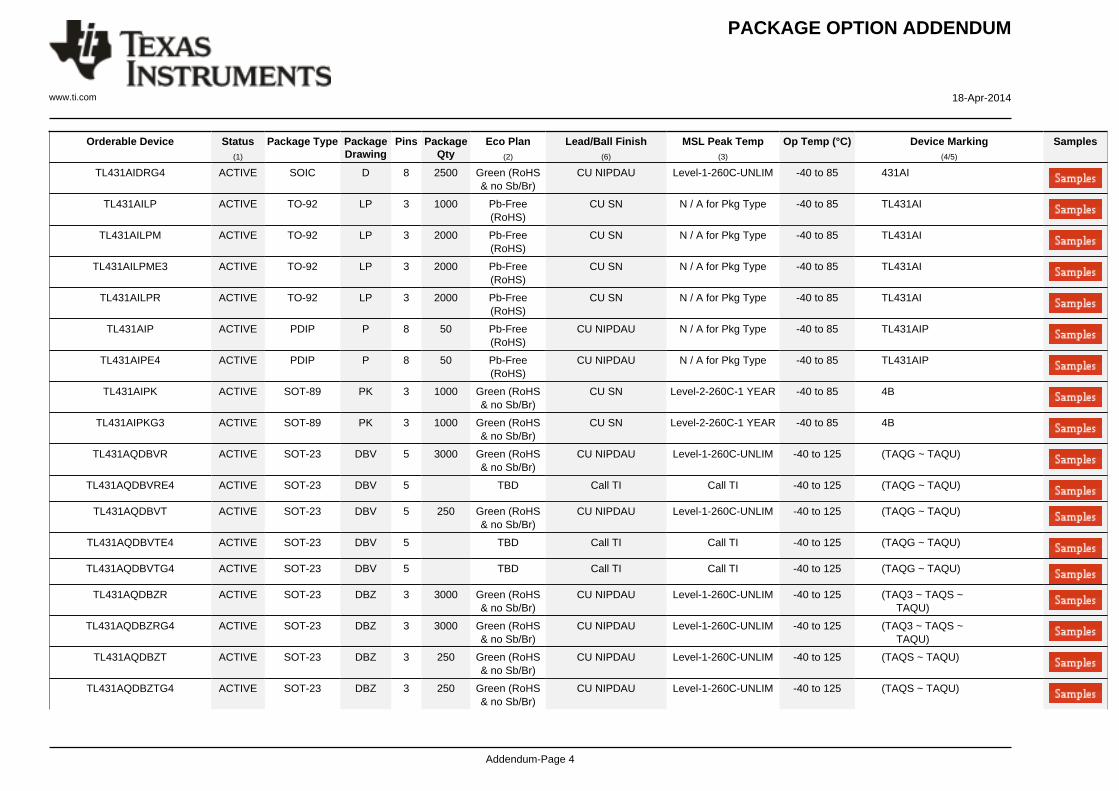
www.ti.com 18-Apr-2014
Addendum-Page 4
Orderable Device Status(1)
Package Type PackageDrawing
Pins PackageQty
Eco Plan(2)
Lead/Ball Finish(6)
MSL Peak Temp(3)
Op Temp (°C) Device Marking(4/5)
Samples
TL431AIDRG4 ACTIVE SOIC D 8 2500 Green (RoHS& no Sb/Br)
CU NIPDAU Level-1-260C-UNLIM -40 to 85 431AI
TL431AILP ACTIVE TO-92 LP 3 1000 Pb-Free(RoHS)
CU SN N / A for Pkg Type -40 to 85 TL431AI
TL431AILPM ACTIVE TO-92 LP 3 2000 Pb-Free(RoHS)
CU SN N / A for Pkg Type -40 to 85 TL431AI
TL431AILPME3 ACTIVE TO-92 LP 3 2000 Pb-Free(RoHS)
CU SN N / A for Pkg Type -40 to 85 TL431AI
TL431AILPR ACTIVE TO-92 LP 3 2000 Pb-Free(RoHS)
CU SN N / A for Pkg Type -40 to 85 TL431AI
TL431AIP ACTIVE PDIP P 8 50 Pb-Free(RoHS)
CU NIPDAU N / A for Pkg Type -40 to 85 TL431AIP
TL431AIPE4 ACTIVE PDIP P 8 50 Pb-Free(RoHS)
CU NIPDAU N / A for Pkg Type -40 to 85 TL431AIP
TL431AIPK ACTIVE SOT-89 PK 3 1000 Green (RoHS& no Sb/Br)
CU SN Level-2-260C-1 YEAR -40 to 85 4B
TL431AIPKG3 ACTIVE SOT-89 PK 3 1000 Green (RoHS& no Sb/Br)
CU SN Level-2-260C-1 YEAR -40 to 85 4B
TL431AQDBVR ACTIVE SOT-23 DBV 5 3000 Green (RoHS& no Sb/Br)
CU NIPDAU Level-1-260C-UNLIM -40 to 125 (TAQG ~ TAQU)
TL431AQDBVRE4 ACTIVE SOT-23 DBV 5 TBD Call TI Call TI -40 to 125 (TAQG ~ TAQU)
TL431AQDBVT ACTIVE SOT-23 DBV 5 250 Green (RoHS& no Sb/Br)
CU NIPDAU Level-1-260C-UNLIM -40 to 125 (TAQG ~ TAQU)
TL431AQDBVTE4 ACTIVE SOT-23 DBV 5 TBD Call TI Call TI -40 to 125 (TAQG ~ TAQU)
TL431AQDBVTG4 ACTIVE SOT-23 DBV 5 TBD Call TI Call TI -40 to 125 (TAQG ~ TAQU)
TL431AQDBZR ACTIVE SOT-23 DBZ 3 3000 Green (RoHS& no Sb/Br)
CU NIPDAU Level-1-260C-UNLIM -40 to 125 (TAQ3 ~ TAQS ~ TAQU)
TL431AQDBZRG4 ACTIVE SOT-23 DBZ 3 3000 Green (RoHS& no Sb/Br)
CU NIPDAU Level-1-260C-UNLIM -40 to 125 (TAQ3 ~ TAQS ~ TAQU)
TL431AQDBZT ACTIVE SOT-23 DBZ 3 250 Green (RoHS& no Sb/Br)
CU NIPDAU Level-1-260C-UNLIM -40 to 125 (TAQS ~ TAQU)
TL431AQDBZTG4 ACTIVE SOT-23 DBZ 3 250 Green (RoHS& no Sb/Br)
CU NIPDAU Level-1-260C-UNLIM -40 to 125 (TAQS ~ TAQU)
PACKAGE OPTION ADDENDUM
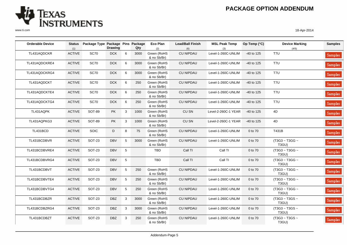
www.ti.com 18-Apr-2014
Addendum-Page 5
Orderable Device Status(1)
Package Type PackageDrawing
Pins PackageQty
Eco Plan(2)
Lead/Ball Finish(6)
MSL Peak Temp(3)
Op Temp (°C) Device Marking(4/5)
Samples
TL431AQDCKR ACTIVE SC70 DCK 6 3000 Green (RoHS& no Sb/Br)
CU NIPDAU Level-1-260C-UNLIM -40 to 125 T7U
TL431AQDCKRE4 ACTIVE SC70 DCK 6 3000 Green (RoHS& no Sb/Br)
CU NIPDAU Level-1-260C-UNLIM -40 to 125 T7U
TL431AQDCKRG4 ACTIVE SC70 DCK 6 3000 Green (RoHS& no Sb/Br)
CU NIPDAU Level-1-260C-UNLIM -40 to 125 T7U
TL431AQDCKT ACTIVE SC70 DCK 6 250 Green (RoHS& no Sb/Br)
CU NIPDAU Level-1-260C-UNLIM -40 to 125 T7U
TL431AQDCKTE4 ACTIVE SC70 DCK 6 250 Green (RoHS& no Sb/Br)
CU NIPDAU Level-1-260C-UNLIM -40 to 125 T7U
TL431AQDCKTG4 ACTIVE SC70 DCK 6 250 Green (RoHS& no Sb/Br)
CU NIPDAU Level-1-260C-UNLIM -40 to 125 T7U
TL431AQPK ACTIVE SOT-89 PK 3 1000 Green (RoHS& no Sb/Br)
CU SN Level-2-260C-1 YEAR -40 to 125 4D
TL431AQPKG3 ACTIVE SOT-89 PK 3 1000 Green (RoHS& no Sb/Br)
CU SN Level-2-260C-1 YEAR -40 to 125 4D
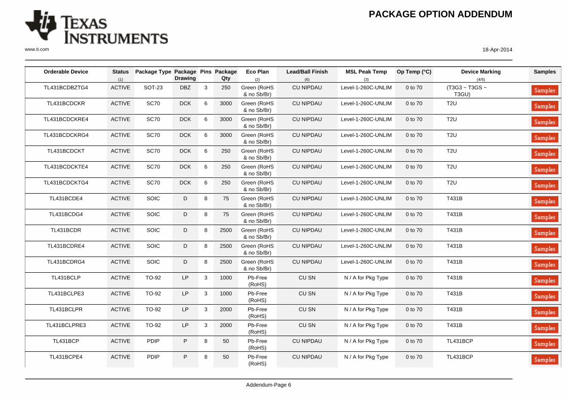
TL431BCD ACTIVE SOIC D 8 75 Green (RoHS& no Sb/Br)
CU NIPDAU Level-1-260C-UNLIM 0 to 70 T431B
TL431BCDBVR ACTIVE SOT-23 DBV 5 3000 Green (RoHS& no Sb/Br)
CU NIPDAU Level-1-260C-UNLIM 0 to 70 (T3G3 ~ T3GG ~ T3GU)
TL431BCDBVRE4 ACTIVE SOT-23 DBV 5 TBD Call TI Call TI 0 to 70 (T3G3 ~ T3GG ~ T3GU)
TL431BCDBVRG4 ACTIVE SOT-23 DBV 5 TBD Call TI Call TI 0 to 70 (T3G3 ~ T3GG ~ T3GU)
TL431BCDBVT ACTIVE SOT-23 DBV 5 250 Green (RoHS& no Sb/Br)
CU NIPDAU Level-1-260C-UNLIM 0 to 70 (T3G3 ~ T3GG ~ T3GU)
TL431BCDBVTE4 ACTIVE SOT-23 DBV 5 250 Green (RoHS& no Sb/Br)
CU NIPDAU Level-1-260C-UNLIM 0 to 70 (T3G3 ~ T3GG ~ T3GU)
TL431BCDBVTG4 ACTIVE SOT-23 DBV 5 250 Green (RoHS& no Sb/Br)
CU NIPDAU Level-1-260C-UNLIM 0 to 70 (T3G3 ~ T3GG ~ T3GU)
TL431BCDBZR ACTIVE SOT-23 DBZ 3 3000 Green (RoHS& no Sb/Br)
CU NIPDAU Level-1-260C-UNLIM 0 to 70 (T3G3 ~ T3GS ~ T3GU)
TL431BCDBZRG4 ACTIVE SOT-23 DBZ 3 3000 Green (RoHS& no Sb/Br)
CU NIPDAU Level-1-260C-UNLIM 0 to 70 (T3G3 ~ T3GS ~ T3GU)
TL431BCDBZT ACTIVE SOT-23 DBZ 3 250 Green (RoHS& no Sb/Br)
CU NIPDAU Level-1-260C-UNLIM 0 to 70 (T3G3 ~ T3GS ~ T3GU)
PACKAGE OPTION ADDENDUM
www.ti.com 18-Apr-2014
Addendum-Page 6
Orderable Device Status(1)
Package Type PackageDrawing
Pins PackageQty
Eco Plan(2)
Lead/Ball Finish(6)
MSL Peak Temp(3)
Op Temp (°C) Device Marking(4/5)
Samples
TL431BCDBZTG4 ACTIVE SOT-23 DBZ 3 250 Green (RoHS& no Sb/Br)
CU NIPDAU Level-1-260C-UNLIM 0 to 70 (T3G3 ~ T3GS ~ T3GU)
TL431BCDCKR ACTIVE SC70 DCK 6 3000 Green (RoHS& no Sb/Br)
CU NIPDAU Level-1-260C-UNLIM 0 to 70 T2U
TL431BCDCKRE4 ACTIVE SC70 DCK 6 3000 Green (RoHS& no Sb/Br)
CU NIPDAU Level-1-260C-UNLIM 0 to 70 T2U
TL431BCDCKRG4 ACTIVE SC70 DCK 6 3000 Green (RoHS& no Sb/Br)
CU NIPDAU Level-1-260C-UNLIM 0 to 70 T2U
TL431BCDCKT ACTIVE SC70 DCK 6 250 Green (RoHS& no Sb/Br)
CU NIPDAU Level-1-260C-UNLIM 0 to 70 T2U
TL431BCDCKTE4 ACTIVE SC70 DCK 6 250 Green (RoHS& no Sb/Br)
CU NIPDAU Level-1-260C-UNLIM 0 to 70 T2U
TL431BCDCKTG4 ACTIVE SC70 DCK 6 250 Green (RoHS& no Sb/Br)
CU NIPDAU Level-1-260C-UNLIM 0 to 70 T2U
TL431BCDE4 ACTIVE SOIC D 8 75 Green (RoHS& no Sb/Br)
CU NIPDAU Level-1-260C-UNLIM 0 to 70 T431B
TL431BCDG4 ACTIVE SOIC D 8 75 Green (RoHS& no Sb/Br)
CU NIPDAU Level-1-260C-UNLIM 0 to 70 T431B
TL431BCDR ACTIVE SOIC D 8 2500 Green (RoHS& no Sb/Br)
CU NIPDAU Level-1-260C-UNLIM 0 to 70 T431B
TL431BCDRE4 ACTIVE SOIC D 8 2500 Green (RoHS& no Sb/Br)
CU NIPDAU Level-1-260C-UNLIM 0 to 70 T431B
TL431BCDRG4 ACTIVE SOIC D 8 2500 Green (RoHS& no Sb/Br)
CU NIPDAU Level-1-260C-UNLIM 0 to 70 T431B
TL431BCLP ACTIVE TO-92 LP 3 1000 Pb-Free(RoHS)
CU SN N / A for Pkg Type 0 to 70 T431B
TL431BCLPE3 ACTIVE TO-92 LP 3 1000 Pb-Free(RoHS)
CU SN N / A for Pkg Type 0 to 70 T431B
TL431BCLPR ACTIVE TO-92 LP 3 2000 Pb-Free(RoHS)
CU SN N / A for Pkg Type 0 to 70 T431B
TL431BCLPRE3 ACTIVE TO-92 LP 3 2000 Pb-Free(RoHS)
CU SN N / A for Pkg Type 0 to 70 T431B
TL431BCP ACTIVE PDIP P 8 50 Pb-Free(RoHS)
CU NIPDAU N / A for Pkg Type 0 to 70 TL431BCP
TL431BCPE4 ACTIVE PDIP P 8 50 Pb-Free(RoHS)
CU NIPDAU N / A for Pkg Type 0 to 70 TL431BCP
PACKAGE OPTION ADDENDUM
www.ti.com 18-Apr-2014
Addendum-Page 7
Orderable Device Status(1)
Package Type PackageDrawing
Pins PackageQty
Eco Plan(2)
Lead/Ball Finish(6)
MSL Peak Temp(3)
Op Temp (°C) Device Marking(4/5)
Samples
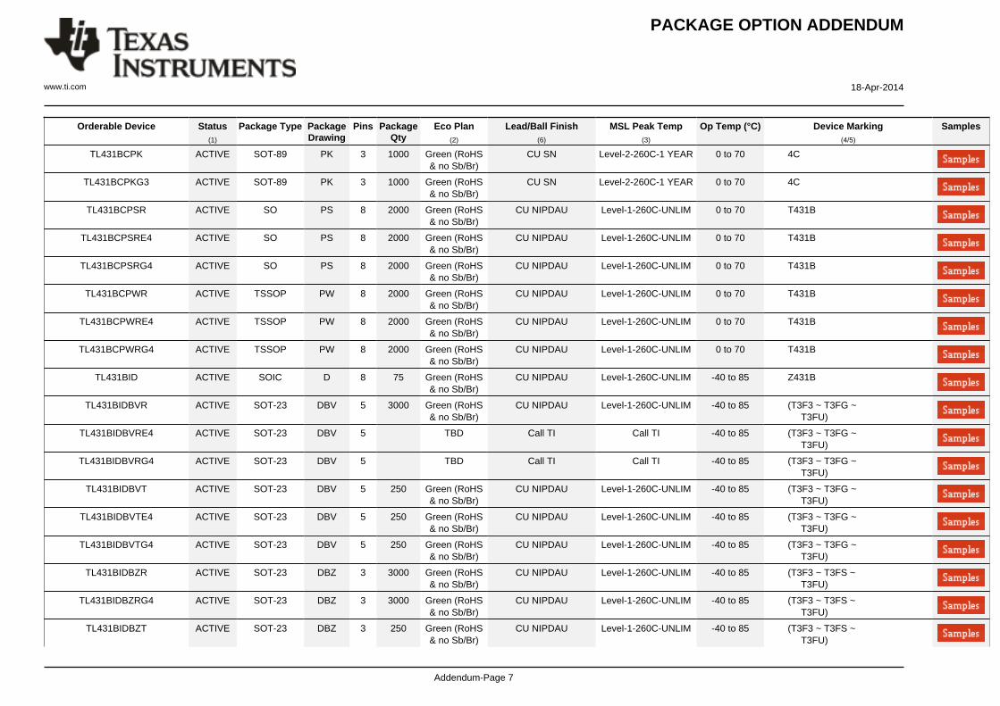
TL431BCPK ACTIVE SOT-89 PK 3 1000 Green (RoHS& no Sb/Br)
CU SN Level-2-260C-1 YEAR 0 to 70 4C
TL431BCPKG3 ACTIVE SOT-89 PK 3 1000 Green (RoHS& no Sb/Br)
CU SN Level-2-260C-1 YEAR 0 to 70 4C
TL431BCPSR ACTIVE SO PS 8 2000 Green (RoHS& no Sb/Br)
CU NIPDAU Level-1-260C-UNLIM 0 to 70 T431B
TL431BCPSRE4 ACTIVE SO PS 8 2000 Green (RoHS& no Sb/Br)
CU NIPDAU Level-1-260C-UNLIM 0 to 70 T431B
TL431BCPSRG4 ACTIVE SO PS 8 2000 Green (RoHS& no Sb/Br)
CU NIPDAU Level-1-260C-UNLIM 0 to 70 T431B
TL431BCPWR ACTIVE TSSOP PW 8 2000 Green (RoHS& no Sb/Br)
CU NIPDAU Level-1-260C-UNLIM 0 to 70 T431B
TL431BCPWRE4 ACTIVE TSSOP PW 8 2000 Green (RoHS& no Sb/Br)
CU NIPDAU Level-1-260C-UNLIM 0 to 70 T431B
TL431BCPWRG4 ACTIVE TSSOP PW 8 2000 Green (RoHS& no Sb/Br)
CU NIPDAU Level-1-260C-UNLIM 0 to 70 T431B
TL431BID ACTIVE SOIC D 8 75 Green (RoHS& no Sb/Br)
CU NIPDAU Level-1-260C-UNLIM -40 to 85 Z431B
TL431BIDBVR ACTIVE SOT-23 DBV 5 3000 Green (RoHS& no Sb/Br)
CU NIPDAU Level-1-260C-UNLIM -40 to 85 (T3F3 ~ T3FG ~ T3FU)
TL431BIDBVRE4 ACTIVE SOT-23 DBV 5 TBD Call TI Call TI -40 to 85 (T3F3 ~ T3FG ~ T3FU)
TL431BIDBVRG4 ACTIVE SOT-23 DBV 5 TBD Call TI Call TI -40 to 85 (T3F3 ~ T3FG ~ T3FU)
TL431BIDBVT ACTIVE SOT-23 DBV 5 250 Green (RoHS& no Sb/Br)
CU NIPDAU Level-1-260C-UNLIM -40 to 85 (T3F3 ~ T3FG ~ T3FU)
TL431BIDBVTE4 ACTIVE SOT-23 DBV 5 250 Green (RoHS& no Sb/Br)
CU NIPDAU Level-1-260C-UNLIM -40 to 85 (T3F3 ~ T3FG ~ T3FU)
TL431BIDBVTG4 ACTIVE SOT-23 DBV 5 250 Green (RoHS& no Sb/Br)
CU NIPDAU Level-1-260C-UNLIM -40 to 85 (T3F3 ~ T3FG ~ T3FU)
TL431BIDBZR ACTIVE SOT-23 DBZ 3 3000 Green (RoHS& no Sb/Br)
CU NIPDAU Level-1-260C-UNLIM -40 to 85 (T3F3 ~ T3FS ~ T3FU)
TL431BIDBZRG4 ACTIVE SOT-23 DBZ 3 3000 Green (RoHS& no Sb/Br)
CU NIPDAU Level-1-260C-UNLIM -40 to 85 (T3F3 ~ T3FS ~ T3FU)
TL431BIDBZT ACTIVE SOT-23 DBZ 3 250 Green (RoHS& no Sb/Br)
CU NIPDAU Level-1-260C-UNLIM -40 to 85 (T3F3 ~ T3FS ~ T3FU)

PACKAGE OPTION ADDENDUM
www.ti.com 18-Apr-2014
Addendum-Page 8
Orderable Device Status(1)
Package Type PackageDrawing
Pins PackageQty
Eco Plan(2)
Lead/Ball Finish(6)
MSL Peak Temp(3)
Op Temp (°C) Device Marking(4/5)
Samples
TL431BIDBZTG4 ACTIVE SOT-23 DBZ 3 250 Green (RoHS& no Sb/Br)
CU NIPDAU Level-1-260C-UNLIM -40 to 85 (T3F3 ~ T3FS ~ T3FU)
TL431BIDCKR ACTIVE SC70 DCK 6 3000 Green (RoHS& no Sb/Br)
CU NIPDAU Level-1-260C-UNLIM -40 to 85 T3U
TL431BIDCKRE4 ACTIVE SC70 DCK 6 3000 Green (RoHS& no Sb/Br)
CU NIPDAU Level-1-260C-UNLIM -40 to 85 T3U
TL431BIDCKRG4 ACTIVE SC70 DCK 6 3000 Green (RoHS& no Sb/Br)
CU NIPDAU Level-1-260C-UNLIM -40 to 85 T3U
TL431BIDCKT ACTIVE SC70 DCK 6 250 Green (RoHS& no Sb/Br)
CU NIPDAU Level-1-260C-UNLIM -40 to 85 T3U
TL431BIDCKTE4 ACTIVE SC70 DCK 6 250 Green (RoHS& no Sb/Br)
CU NIPDAU Level-1-260C-UNLIM -40 to 85 T3U
TL431BIDCKTG4 ACTIVE SC70 DCK 6 250 Green (RoHS& no Sb/Br)
CU NIPDAU Level-1-260C-UNLIM -40 to 85 T3U
TL431BIDE4 ACTIVE SOIC D 8 75 Green (RoHS& no Sb/Br)
CU NIPDAU Level-1-260C-UNLIM -40 to 85 Z431B
TL431BIDG4 ACTIVE SOIC D 8 75 Green (RoHS& no Sb/Br)
CU NIPDAU Level-1-260C-UNLIM -40 to 85 Z431B
TL431BIDR ACTIVE SOIC D 8 2500 Green (RoHS& no Sb/Br)
CU NIPDAU | CU SN Level-1-260C-UNLIM -40 to 85 Z431B
TL431BIDRE4 ACTIVE SOIC D 8 2500 Green (RoHS& no Sb/Br)
CU NIPDAU Level-1-260C-UNLIM -40 to 85 Z431B
TL431BIDRG4 ACTIVE SOIC D 8 2500 Green (RoHS& no Sb/Br)
CU NIPDAU Level-1-260C-UNLIM -40 to 85 Z431B
TL431BILP ACTIVE TO-92 LP 3 1000 Pb-Free(RoHS)
CU SN N / A for Pkg Type -40 to 85 Z431B
TL431BILPE3 ACTIVE TO-92 LP 3 1000 Pb-Free(RoHS)
CU SN N / A for Pkg Type -40 to 85 Z431B
TL431BILPR ACTIVE TO-92 LP 3 2000 Pb-Free(RoHS)
CU SN N / A for Pkg Type -40 to 85 Z431B
TL431BILPRE3 ACTIVE TO-92 LP 3 2000 Pb-Free(RoHS)
CU SN N / A for Pkg Type -40 to 85 Z431B
TL431BIP ACTIVE PDIP P 8 50 Pb-Free(RoHS)
CU NIPDAU N / A for Pkg Type -40 to 85 TL431BIP
TL431BIPE4 ACTIVE PDIP P 8 50 Pb-Free(RoHS)
CU NIPDAU N / A for Pkg Type -40 to 85 TL431BIP
PACKAGE OPTION ADDENDUM
www.ti.com 18-Apr-2014
Addendum-Page 9
Orderable Device Status(1)
Package Type PackageDrawing
Pins PackageQty
Eco Plan(2)
Lead/Ball Finish(6)
MSL Peak Temp(3)
Op Temp (°C) Device Marking(4/5)
Samples
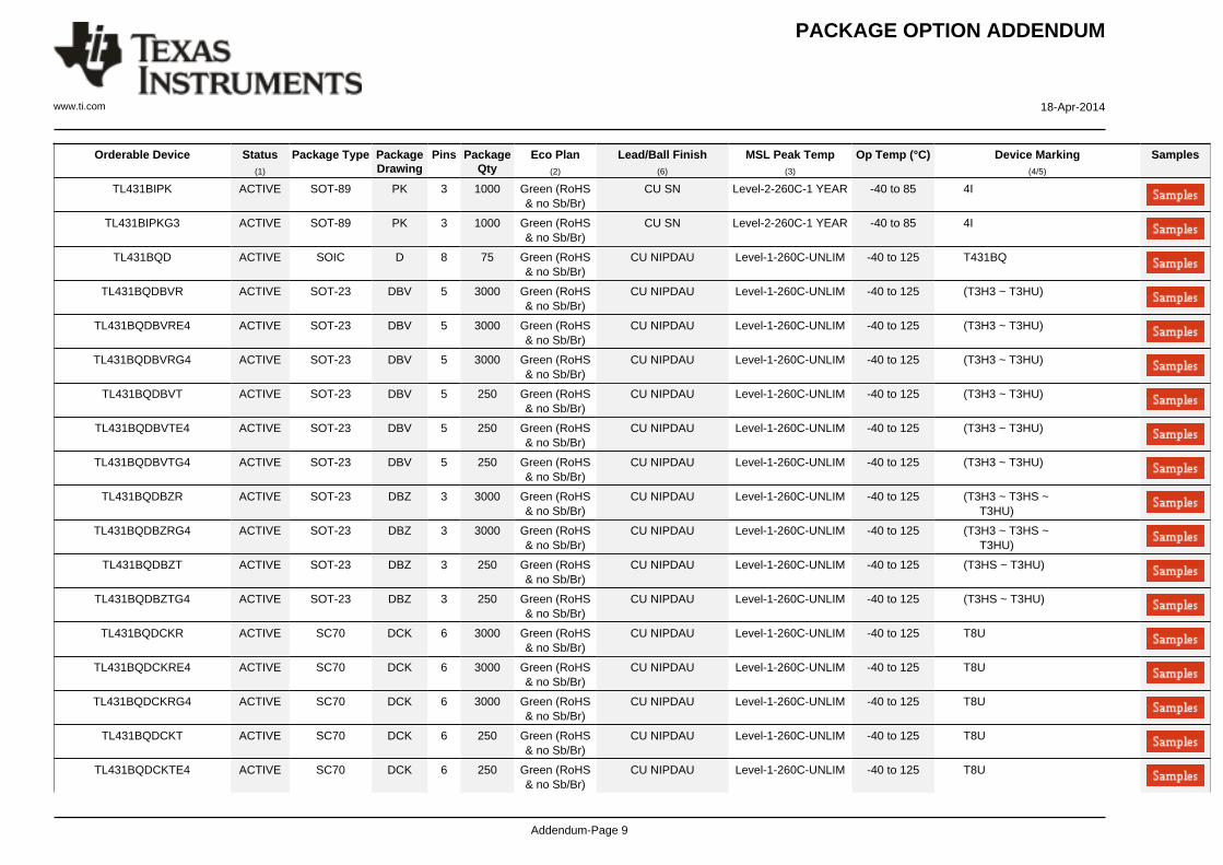
TL431BIPK ACTIVE SOT-89 PK 3 1000 Green (RoHS& no Sb/Br)
CU SN Level-2-260C-1 YEAR -40 to 85 4I
TL431BIPKG3 ACTIVE SOT-89 PK 3 1000 Green (RoHS& no Sb/Br)
CU SN Level-2-260C-1 YEAR -40 to 85 4I
TL431BQD ACTIVE SOIC D 8 75 Green (RoHS& no Sb/Br)
CU NIPDAU Level-1-260C-UNLIM -40 to 125 T431BQ
TL431BQDBVR ACTIVE SOT-23 DBV 5 3000 Green (RoHS& no Sb/Br)
CU NIPDAU Level-1-260C-UNLIM -40 to 125 (T3H3 ~ T3HU)
TL431BQDBVRE4 ACTIVE SOT-23 DBV 5 3000 Green (RoHS& no Sb/Br)
CU NIPDAU Level-1-260C-UNLIM -40 to 125 (T3H3 ~ T3HU)
TL431BQDBVRG4 ACTIVE SOT-23 DBV 5 3000 Green (RoHS& no Sb/Br)
CU NIPDAU Level-1-260C-UNLIM -40 to 125 (T3H3 ~ T3HU)
TL431BQDBVT ACTIVE SOT-23 DBV 5 250 Green (RoHS& no Sb/Br)
CU NIPDAU Level-1-260C-UNLIM -40 to 125 (T3H3 ~ T3HU)
TL431BQDBVTE4 ACTIVE SOT-23 DBV 5 250 Green (RoHS& no Sb/Br)
CU NIPDAU Level-1-260C-UNLIM -40 to 125 (T3H3 ~ T3HU)
TL431BQDBVTG4 ACTIVE SOT-23 DBV 5 250 Green (RoHS& no Sb/Br)
CU NIPDAU Level-1-260C-UNLIM -40 to 125 (T3H3 ~ T3HU)
TL431BQDBZR ACTIVE SOT-23 DBZ 3 3000 Green (RoHS& no Sb/Br)
CU NIPDAU Level-1-260C-UNLIM -40 to 125 (T3H3 ~ T3HS ~ T3HU)
TL431BQDBZRG4 ACTIVE SOT-23 DBZ 3 3000 Green (RoHS& no Sb/Br)
CU NIPDAU Level-1-260C-UNLIM -40 to 125 (T3H3 ~ T3HS ~ T3HU)
TL431BQDBZT ACTIVE SOT-23 DBZ 3 250 Green (RoHS& no Sb/Br)
CU NIPDAU Level-1-260C-UNLIM -40 to 125 (T3HS ~ T3HU)
TL431BQDBZTG4 ACTIVE SOT-23 DBZ 3 250 Green (RoHS& no Sb/Br)
CU NIPDAU Level-1-260C-UNLIM -40 to 125 (T3HS ~ T3HU)
TL431BQDCKR ACTIVE SC70 DCK 6 3000 Green (RoHS& no Sb/Br)
CU NIPDAU Level-1-260C-UNLIM -40 to 125 T8U
TL431BQDCKRE4 ACTIVE SC70 DCK 6 3000 Green (RoHS& no Sb/Br)
CU NIPDAU Level-1-260C-UNLIM -40 to 125 T8U
TL431BQDCKRG4 ACTIVE SC70 DCK 6 3000 Green (RoHS& no Sb/Br)
CU NIPDAU Level-1-260C-UNLIM -40 to 125 T8U
TL431BQDCKT ACTIVE SC70 DCK 6 250 Green (RoHS& no Sb/Br)
CU NIPDAU Level-1-260C-UNLIM -40 to 125 T8U
TL431BQDCKTE4 ACTIVE SC70 DCK 6 250 Green (RoHS& no Sb/Br)
CU NIPDAU Level-1-260C-UNLIM -40 to 125 T8U

PACKAGE OPTION ADDENDUM
www.ti.com 18-Apr-2014
Addendum-Page 10
Orderable Device Status(1)
Package Type PackageDrawing
Pins PackageQty
Eco Plan(2)
Lead/Ball Finish(6)
MSL Peak Temp(3)
Op Temp (°C) Device Marking(4/5)
Samples
TL431BQDCKTG4 ACTIVE SC70 DCK 6 250 Green (RoHS& no Sb/Br)
CU NIPDAU Level-1-260C-UNLIM -40 to 125 T8U
TL431BQDE4 ACTIVE SOIC D 8 75 Green (RoHS& no Sb/Br)
CU NIPDAU Level-1-260C-UNLIM -40 to 125 T431BQ
TL431BQDG4 ACTIVE SOIC D 8 75 Green (RoHS& no Sb/Br)
CU NIPDAU Level-1-260C-UNLIM -40 to 125 T431BQ
TL431BQDR ACTIVE SOIC D 8 2500 Green (RoHS& no Sb/Br)
CU NIPDAU Level-1-260C-UNLIM -40 to 125 T431BQ
TL431BQDRE4 ACTIVE SOIC D 8 2500 Green (RoHS& no Sb/Br)
CU NIPDAU Level-1-260C-UNLIM -40 to 125 T431BQ
TL431BQDRG4 ACTIVE SOIC D 8 2500 Green (RoHS& no Sb/Br)
CU NIPDAU Level-1-260C-UNLIM -40 to 125 T431BQ
TL431BQLP ACTIVE TO-92 LP 3 1000 Pb-Free(RoHS)
CU SN N / A for Pkg Type -40 to 125 T431BQ
TL431BQLPE3 ACTIVE TO-92 LP 3 1000 Pb-Free(RoHS)
CU SN N / A for Pkg Type -40 to 125 T431BQ
TL431BQLPM ACTIVE TO-92 LP 3 2000 Pb-Free(RoHS)
CU SN N / A for Pkg Type -40 to 125 T431BQ
TL431BQLPME3 ACTIVE TO-92 LP 3 2000 Pb-Free(RoHS)
CU SN N / A for Pkg Type -40 to 125 T431BQ
TL431BQLPR ACTIVE TO-92 LP 3 2000 Pb-Free(RoHS)
CU SN N / A for Pkg Type -40 to 125 T431BQ
TL431BQLPRE3 ACTIVE TO-92 LP 3 2000 Pb-Free(RoHS)
CU SN N / A for Pkg Type -40 to 125 T431BQ
TL431BQPK ACTIVE SOT-89 PK 3 1000 Green (RoHS& no Sb/Br)
CU SN Level-2-260C-1 YEAR -40 to 125 3H
TL431BQPKG3 ACTIVE SOT-89 PK 3 1000 Green (RoHS& no Sb/Br)
CU SN Level-2-260C-1 YEAR -40 to 125 3H
TL431BQPSR PREVIEW SO PS 8 2000 TBD Call TI Call TI -40 to 125 T431BQ
TL431CD ACTIVE SOIC D 8 75 Green (RoHS& no Sb/Br)
CU NIPDAU Level-1-260C-UNLIM 0 to 70 TL431C
TL431CDBVR ACTIVE SOT-23 DBV 5 3000 Green (RoHS& no Sb/Br)
CU NIPDAU Level-1-260C-UNLIM 0 to 70 (T3C3 ~ T3CG ~ T3CS)
TL431CDBVRE4 ACTIVE SOT-23 DBV 5 3000 Green (RoHS& no Sb/Br)
CU NIPDAU Level-1-260C-UNLIM 0 to 70 (T3C3 ~ T3CG ~ T3CS)
PACKAGE OPTION ADDENDUM
www.ti.com 18-Apr-2014
Addendum-Page 11
Orderable Device Status(1)
Package Type PackageDrawing
Pins PackageQty
Eco Plan(2)
Lead/Ball Finish(6)
MSL Peak Temp(3)
Op Temp (°C) Device Marking(4/5)
Samples
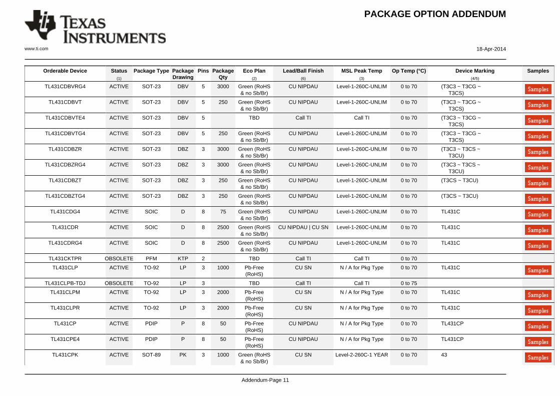
TL431CDBVRG4 ACTIVE SOT-23 DBV 5 3000 Green (RoHS& no Sb/Br)
CU NIPDAU Level-1-260C-UNLIM 0 to 70 (T3C3 ~ T3CG ~ T3CS)
TL431CDBVT ACTIVE SOT-23 DBV 5 250 Green (RoHS& no Sb/Br)
CU NIPDAU Level-1-260C-UNLIM 0 to 70 (T3C3 ~ T3CG ~ T3CS)
TL431CDBVTE4 ACTIVE SOT-23 DBV 5 TBD Call TI Call TI 0 to 70 (T3C3 ~ T3CG ~ T3CS)
TL431CDBVTG4 ACTIVE SOT-23 DBV 5 250 Green (RoHS& no Sb/Br)
CU NIPDAU Level-1-260C-UNLIM 0 to 70 (T3C3 ~ T3CG ~ T3CS)
TL431CDBZR ACTIVE SOT-23 DBZ 3 3000 Green (RoHS& no Sb/Br)
CU NIPDAU Level-1-260C-UNLIM 0 to 70 (T3C3 ~ T3CS ~ T3CU)
TL431CDBZRG4 ACTIVE SOT-23 DBZ 3 3000 Green (RoHS& no Sb/Br)
CU NIPDAU Level-1-260C-UNLIM 0 to 70 (T3C3 ~ T3CS ~ T3CU)
TL431CDBZT ACTIVE SOT-23 DBZ 3 250 Green (RoHS& no Sb/Br)
CU NIPDAU Level-1-260C-UNLIM 0 to 70 (T3CS ~ T3CU)
TL431CDBZTG4 ACTIVE SOT-23 DBZ 3 250 Green (RoHS& no Sb/Br)
CU NIPDAU Level-1-260C-UNLIM 0 to 70 (T3CS ~ T3CU)
TL431CDG4 ACTIVE SOIC D 8 75 Green (RoHS& no Sb/Br)
CU NIPDAU Level-1-260C-UNLIM 0 to 70 TL431C
TL431CDR ACTIVE SOIC D 8 2500 Green (RoHS& no Sb/Br)
CU NIPDAU | CU SN Level-1-260C-UNLIM 0 to 70 TL431C
TL431CDRG4 ACTIVE SOIC D 8 2500 Green (RoHS& no Sb/Br)
CU NIPDAU Level-1-260C-UNLIM 0 to 70 TL431C
TL431CKTPR OBSOLETE PFM KTP 2 TBD Call TI Call TI 0 to 70
TL431CLP ACTIVE TO-92 LP 3 1000 Pb-Free(RoHS)
CU SN N / A for Pkg Type 0 to 70 TL431C
TL431CLPB-TDJ OBSOLETE TO-92 LP 3 TBD Call TI Call TI 0 to 75
TL431CLPM ACTIVE TO-92 LP 3 2000 Pb-Free(RoHS)
CU SN N / A for Pkg Type 0 to 70 TL431C
TL431CLPR ACTIVE TO-92 LP 3 2000 Pb-Free(RoHS)
CU SN N / A for Pkg Type 0 to 70 TL431C
TL431CP ACTIVE PDIP P 8 50 Pb-Free(RoHS)
CU NIPDAU N / A for Pkg Type 0 to 70 TL431CP
TL431CPE4 ACTIVE PDIP P 8 50 Pb-Free(RoHS)
CU NIPDAU N / A for Pkg Type 0 to 70 TL431CP
TL431CPK ACTIVE SOT-89 PK 3 1000 Green (RoHS& no Sb/Br)
CU SN Level-2-260C-1 YEAR 0 to 70 43
PACKAGE OPTION ADDENDUM
www.ti.com 18-Apr-2014
Addendum-Page 12
Orderable Device Status(1)
Package Type PackageDrawing
Pins PackageQty
Eco Plan(2)
Lead/Ball Finish(6)
MSL Peak Temp(3)
Op Temp (°C) Device Marking(4/5)
Samples
TL431CPKG3 ACTIVE SOT-89 PK 3 1000 Green (RoHS& no Sb/Br)
CU SN Level-2-260C-1 YEAR 0 to 70 43
TL431CPSLE OBSOLETE SO PS 8 TBD Call TI Call TI 0 to 70
TL431CPSR ACTIVE SO PS 8 2000 Green (RoHS& no Sb/Br)
CU NIPDAU Level-1-260C-UNLIM 0 to 70 T431
TL431CPSRG4 ACTIVE SO PS 8 2000 Green (RoHS& no Sb/Br)
CU NIPDAU Level-1-260C-UNLIM 0 to 70 T431
TL431CPW OBSOLETE TSSOP PW 8 TBD Call TI Call TI 0 to 70 T431
TL431CPWE4 OBSOLETE TSSOP PW 8 TBD Call TI Call TI 0 to 70
TL431CPWG4 OBSOLETE TSSOP PW 8 TBD Call TI Call TI 0 to 70
TL431CPWLE OBSOLETE TSSOP PW 8 TBD Call TI Call TI 0 to 70
TL431CPWR ACTIVE TSSOP PW 8 2000 Green (RoHS& no Sb/Br)
CU NIPDAU Level-1-260C-UNLIM 0 to 70 T431
TL431CPWRE4 ACTIVE TSSOP PW 8 2000 Green (RoHS& no Sb/Br)
CU NIPDAU Level-1-260C-UNLIM 0 to 70 T431
TL431CPWRG4 ACTIVE TSSOP PW 8 2000 Green (RoHS& no Sb/Br)
CU NIPDAU Level-1-260C-UNLIM 0 to 70 T431
TL431ID ACTIVE SOIC D 8 75 Green (RoHS& no Sb/Br)
CU NIPDAU Level-1-260C-UNLIM -40 to 85 TL431I
TL431IDBVR ACTIVE SOT-23 DBV 5 3000 Green (RoHS& no Sb/Br)
CU NIPDAU Level-1-260C-UNLIM -40 to 85 (T3I3 ~ T3IG ~ T3IS)
TL431IDBVRE4 ACTIVE SOT-23 DBV 5 3000 Green (RoHS& no Sb/Br)
CU NIPDAU Level-1-260C-UNLIM -40 to 85 (T3I3 ~ T3IG ~ T3IS)
TL431IDBVRG4 ACTIVE SOT-23 DBV 5 3000 Green (RoHS& no Sb/Br)
CU NIPDAU Level-1-260C-UNLIM -40 to 85 (T3I3 ~ T3IG ~ T3IS)
TL431IDBVT ACTIVE SOT-23 DBV 5 250 Green (RoHS& no Sb/Br)
CU NIPDAU Level-1-260C-UNLIM -40 to 85 (T3I3 ~ T3IG ~ T3IU)
TL431IDBVTE4 ACTIVE SOT-23 DBV 5 TBD Call TI Call TI -40 to 85 (T3I3 ~ T3IG ~ T3IU)
TL431IDBVTG4 ACTIVE SOT-23 DBV 5 TBD Call TI Call TI -40 to 85 (T3I3 ~ T3IG ~ T3IU)
TL431IDBZR ACTIVE SOT-23 DBZ 3 3000 Green (RoHS& no Sb/Br)
CU NIPDAU Level-1-260C-UNLIM -40 to 85 (T3I3 ~ T3IS ~ T3IU)
TL431IDBZRG4 ACTIVE SOT-23 DBZ 3 3000 Green (RoHS& no Sb/Br)
CU NIPDAU Level-1-260C-UNLIM -40 to 85 (T3I3 ~ T3IS ~ T3IU)
PACKAGE OPTION ADDENDUM
www.ti.com 18-Apr-2014
Addendum-Page 13
Orderable Device Status(1)
Package Type PackageDrawing
Pins PackageQty
Eco Plan(2)
Lead/Ball Finish(6)
MSL Peak Temp(3)
Op Temp (°C) Device Marking(4/5)
Samples
TL431IDBZT ACTIVE SOT-23 DBZ 3 250 Green (RoHS& no Sb/Br)
CU NIPDAU Level-1-260C-UNLIM -40 to 85 (T3IS ~ T3IU)
TL431IDBZTG4 ACTIVE SOT-23 DBZ 3 250 Green (RoHS& no Sb/Br)
CU NIPDAU Level-1-260C-UNLIM -40 to 85 (T3IS ~ T3IU)
TL431IDG4 ACTIVE SOIC D 8 75 Green (RoHS& no Sb/Br)
CU NIPDAU Level-1-260C-UNLIM -40 to 85 TL431I
TL431IDR ACTIVE SOIC D 8 2500 Green (RoHS& no Sb/Br)
CU NIPDAU | CU SN Level-1-260C-UNLIM -40 to 85 TL431I
TL431IDRG4 ACTIVE SOIC D 8 2500 Green (RoHS& no Sb/Br)
CU NIPDAU Level-1-260C-UNLIM -40 to 85 TL431I
TL431ILP ACTIVE TO-92 LP 3 1000 Pb-Free(RoHS)
CU SN N / A for Pkg Type -40 to 85 TL431I
TL431ILPM OBSOLETE TO-92 LP 3 TBD Call TI Call TI -40 to 85
TL431ILPR ACTIVE TO-92 LP 3 2000 Pb-Free(RoHS)
CU SN N / A for Pkg Type -40 to 85 TL431I
TL431IP ACTIVE PDIP P 8 50 Pb-Free(RoHS)
CU NIPDAU N / A for Pkg Type -40 to 85 TL431IP
TL431IPE4 ACTIVE PDIP P 8 50 Pb-Free(RoHS)
CU NIPDAU N / A for Pkg Type -40 to 85 TL431IP
TL431IPK ACTIVE SOT-89 PK 3 1000 Green (RoHS& no Sb/Br)
CU SN Level-2-260C-1 YEAR -40 to 85 3I
TL431IPKG3 ACTIVE SOT-89 PK 3 1000 Green (RoHS& no Sb/Br)
CU SN Level-2-260C-1 YEAR -40 to 85 3I
TL431MFKB OBSOLETE LCCC FK 20 TBD Call TI Call TI -55 to 125
TL431MJG OBSOLETE CDIP JG 8 TBD Call TI Call TI -55 to 125
TL431MJGB OBSOLETE CDIP JG 8 TBD Call TI Call TI -55 to 125
TL431QD ACTIVE SOIC D 8 75 Green (RoHS& no Sb/Br)
CU NIPDAU Level-1-260C-UNLIM -40 to 125 T431Q
TL431QDBVR ACTIVE SOT-23 DBV 5 3000 Green (RoHS& no Sb/Br)
CU NIPDAU Level-1-260C-UNLIM -40 to 125 (T3QG ~ T3QU)
TL431QDBVRE4 ACTIVE SOT-23 DBV 5 TBD Call TI Call TI -40 to 125 (T3QG ~ T3QU)
TL431QDBVRG4 ACTIVE SOT-23 DBV 5 3000 Green (RoHS& no Sb/Br)
CU NIPDAU Level-1-260C-UNLIM -40 to 125 (T3QG ~ T3QU)
TL431QDBVT ACTIVE SOT-23 DBV 5 250 Green (RoHS& no Sb/Br)
CU NIPDAU Level-1-260C-UNLIM -40 to 125 (T3QG ~ T3QU)
PACKAGE OPTION ADDENDUM
www.ti.com 18-Apr-2014
Addendum-Page 14
Orderable Device Status(1)
Package Type PackageDrawing
Pins PackageQty
Eco Plan(2)
Lead/Ball Finish(6)
MSL Peak Temp(3)
Op Temp (°C) Device Marking(4/5)
Samples
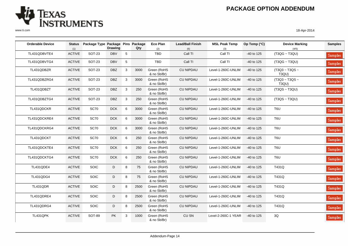
TL431QDBVTE4 ACTIVE SOT-23 DBV 5 TBD Call TI Call TI -40 to 125 (T3QG ~ T3QU)
TL431QDBVTG4 ACTIVE SOT-23 DBV 5 TBD Call TI Call TI -40 to 125 (T3QG ~ T3QU)
TL431QDBZR ACTIVE SOT-23 DBZ 3 3000 Green (RoHS& no Sb/Br)
CU NIPDAU Level-1-260C-UNLIM -40 to 125 (T3Q3 ~ T3QS ~ T3QU)
TL431QDBZRG4 ACTIVE SOT-23 DBZ 3 3000 Green (RoHS& no Sb/Br)
CU NIPDAU Level-1-260C-UNLIM -40 to 125 (T3Q3 ~ T3QS ~ T3QU)
TL431QDBZT ACTIVE SOT-23 DBZ 3 250 Green (RoHS& no Sb/Br)
CU NIPDAU Level-1-260C-UNLIM -40 to 125 (T3QS ~ T3QU)
TL431QDBZTG4 ACTIVE SOT-23 DBZ 3 250 Green (RoHS& no Sb/Br)
CU NIPDAU Level-1-260C-UNLIM -40 to 125 (T3QS ~ T3QU)
TL431QDCKR ACTIVE SC70 DCK 6 3000 Green (RoHS& no Sb/Br)
CU NIPDAU Level-1-260C-UNLIM -40 to 125 T6U
TL431QDCKRE4 ACTIVE SC70 DCK 6 3000 Green (RoHS& no Sb/Br)
CU NIPDAU Level-1-260C-UNLIM -40 to 125 T6U
TL431QDCKRG4 ACTIVE SC70 DCK 6 3000 Green (RoHS& no Sb/Br)
CU NIPDAU Level-1-260C-UNLIM -40 to 125 T6U
TL431QDCKT ACTIVE SC70 DCK 6 250 Green (RoHS& no Sb/Br)
CU NIPDAU Level-1-260C-UNLIM -40 to 125 T6U
TL431QDCKTE4 ACTIVE SC70 DCK 6 250 Green (RoHS& no Sb/Br)
CU NIPDAU Level-1-260C-UNLIM -40 to 125 T6U
TL431QDCKTG4 ACTIVE SC70 DCK 6 250 Green (RoHS& no Sb/Br)
CU NIPDAU Level-1-260C-UNLIM -40 to 125 T6U
TL431QDE4 ACTIVE SOIC D 8 75 Green (RoHS& no Sb/Br)
CU NIPDAU Level-1-260C-UNLIM -40 to 125 T431Q
TL431QDG4 ACTIVE SOIC D 8 75 Green (RoHS& no Sb/Br)
CU NIPDAU Level-1-260C-UNLIM -40 to 125 T431Q
TL431QDR ACTIVE SOIC D 8 2500 Green (RoHS& no Sb/Br)
CU NIPDAU Level-1-260C-UNLIM -40 to 125 T431Q
TL431QDRE4 ACTIVE SOIC D 8 2500 Green (RoHS& no Sb/Br)
CU NIPDAU Level-1-260C-UNLIM -40 to 125 T431Q
TL431QDRG4 ACTIVE SOIC D 8 2500 Green (RoHS& no Sb/Br)
CU NIPDAU Level-1-260C-UNLIM -40 to 125 T431Q
TL431QPK ACTIVE SOT-89 PK 3 1000 Green (RoHS& no Sb/Br)
CU SN Level-2-260C-1 YEAR -40 to 125 3Q
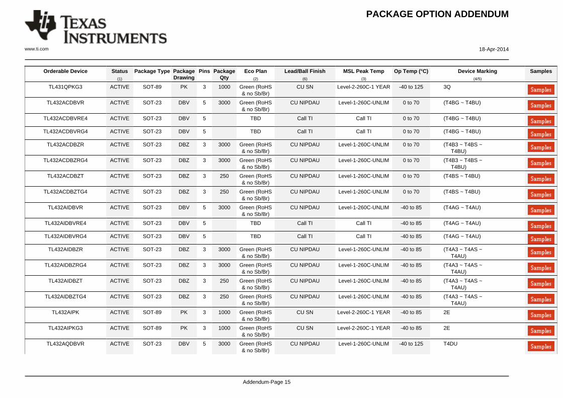
PACKAGE OPTION ADDENDUM
www.ti.com 18-Apr-2014
Addendum-Page 15
Orderable Device Status(1)
Package Type PackageDrawing
Pins PackageQty
Eco Plan(2)
Lead/Ball Finish(6)
MSL Peak Temp(3)
Op Temp (°C) Device Marking(4/5)
Samples
TL431QPKG3 ACTIVE SOT-89 PK 3 1000 Green (RoHS& no Sb/Br)
CU SN Level-2-260C-1 YEAR -40 to 125 3Q
TL432ACDBVR ACTIVE SOT-23 DBV 5 3000 Green (RoHS& no Sb/Br)
CU NIPDAU Level-1-260C-UNLIM 0 to 70 (T4BG ~ T4BU)
TL432ACDBVRE4 ACTIVE SOT-23 DBV 5 TBD Call TI Call TI 0 to 70 (T4BG ~ T4BU)
TL432ACDBVRG4 ACTIVE SOT-23 DBV 5 TBD Call TI Call TI 0 to 70 (T4BG ~ T4BU)
TL432ACDBZR ACTIVE SOT-23 DBZ 3 3000 Green (RoHS& no Sb/Br)
CU NIPDAU Level-1-260C-UNLIM 0 to 70 (T4B3 ~ T4BS ~ T4BU)
TL432ACDBZRG4 ACTIVE SOT-23 DBZ 3 3000 Green (RoHS& no Sb/Br)
CU NIPDAU Level-1-260C-UNLIM 0 to 70 (T4B3 ~ T4BS ~ T4BU)
TL432ACDBZT ACTIVE SOT-23 DBZ 3 250 Green (RoHS& no Sb/Br)
CU NIPDAU Level-1-260C-UNLIM 0 to 70 (T4BS ~ T4BU)
TL432ACDBZTG4 ACTIVE SOT-23 DBZ 3 250 Green (RoHS& no Sb/Br)
CU NIPDAU Level-1-260C-UNLIM 0 to 70 (T4BS ~ T4BU)
TL432AIDBVR ACTIVE SOT-23 DBV 5 3000 Green (RoHS& no Sb/Br)
CU NIPDAU Level-1-260C-UNLIM -40 to 85 (T4AG ~ T4AU)
TL432AIDBVRE4 ACTIVE SOT-23 DBV 5 TBD Call TI Call TI -40 to 85 (T4AG ~ T4AU)
TL432AIDBVRG4 ACTIVE SOT-23 DBV 5 TBD Call TI Call TI -40 to 85 (T4AG ~ T4AU)
TL432AIDBZR ACTIVE SOT-23 DBZ 3 3000 Green (RoHS& no Sb/Br)
CU NIPDAU Level-1-260C-UNLIM -40 to 85 (T4A3 ~ T4AS ~ T4AU)
TL432AIDBZRG4 ACTIVE SOT-23 DBZ 3 3000 Green (RoHS& no Sb/Br)
CU NIPDAU Level-1-260C-UNLIM -40 to 85 (T4A3 ~ T4AS ~ T4AU)
TL432AIDBZT ACTIVE SOT-23 DBZ 3 250 Green (RoHS& no Sb/Br)
CU NIPDAU Level-1-260C-UNLIM -40 to 85 (T4A3 ~ T4AS ~ T4AU)
TL432AIDBZTG4 ACTIVE SOT-23 DBZ 3 250 Green (RoHS& no Sb/Br)
CU NIPDAU Level-1-260C-UNLIM -40 to 85 (T4A3 ~ T4AS ~ T4AU)
TL432AIPK ACTIVE SOT-89 PK 3 1000 Green (RoHS& no Sb/Br)
CU SN Level-2-260C-1 YEAR -40 to 85 2E
TL432AIPKG3 ACTIVE SOT-89 PK 3 1000 Green (RoHS& no Sb/Br)
CU SN Level-2-260C-1 YEAR -40 to 85 2E
TL432AQDBVR ACTIVE SOT-23 DBV 5 3000 Green (RoHS& no Sb/Br)
CU NIPDAU Level-1-260C-UNLIM -40 to 125 T4DU

PACKAGE OPTION ADDENDUM
www.ti.com 18-Apr-2014
Addendum-Page 16
Orderable Device Status(1)
Package Type PackageDrawing
Pins PackageQty
Eco Plan(2)
Lead/Ball Finish(6)
MSL Peak Temp(3)
Op Temp (°C) Device Marking(4/5)
Samples
TL432AQDBVRE4 ACTIVE SOT-23 DBV 5 3000 Green (RoHS& no Sb/Br)
CU NIPDAU Level-1-260C-UNLIM -40 to 125 T4DU
TL432AQDBVRG4 ACTIVE SOT-23 DBV 5 3000 Green (RoHS& no Sb/Br)
CU NIPDAU Level-1-260C-UNLIM -40 to 125 T4DU
TL432AQDBVT ACTIVE SOT-23 DBV 5 250 Green (RoHS& no Sb/Br)
CU NIPDAU Level-1-260C-UNLIM -40 to 125 T4DU
TL432AQDBVTE4 ACTIVE SOT-23 DBV 5 250 Green (RoHS& no Sb/Br)
CU NIPDAU Level-1-260C-UNLIM -40 to 125 T4DU
TL432AQDBVTG4 ACTIVE SOT-23 DBV 5 250 Green (RoHS& no Sb/Br)
CU NIPDAU Level-1-260C-UNLIM -40 to 125 T4DU
TL432AQDBZR ACTIVE SOT-23 DBZ 3 3000 Green (RoHS& no Sb/Br)
CU NIPDAU Level-1-260C-UNLIM -40 to 125 (T4D3 ~ T4DS ~ T4DU)
TL432AQDBZRG4 ACTIVE SOT-23 DBZ 3 3000 Green (RoHS& no Sb/Br)
CU NIPDAU Level-1-260C-UNLIM -40 to 125 (T4D3 ~ T4DS ~ T4DU)
TL432AQDBZT ACTIVE SOT-23 DBZ 3 250 Green (RoHS& no Sb/Br)
CU NIPDAU Level-1-260C-UNLIM -40 to 125 (T4DS ~ T4DU)
TL432AQDBZTG4 ACTIVE SOT-23 DBZ 3 250 Green (RoHS& no Sb/Br)
CU NIPDAU Level-1-260C-UNLIM -40 to 125 (T4DS ~ T4DU)
TL432AQPK ACTIVE SOT-89 PK 3 1000 Green (RoHS& no Sb/Br)
CU SN Level-2-260C-1 YEAR -40 to 125 2F
TL432AQPKG3 ACTIVE SOT-89 PK 3 1000 Green (RoHS& no Sb/Br)
CU SN Level-2-260C-1 YEAR -40 to 125 2F
TL432BCDBVR ACTIVE SOT-23 DBV 5 3000 Green (RoHS& no Sb/Br)
CU NIPDAU Level-1-260C-UNLIM 0 to 70 (TBC3 ~ TBCU)
TL432BCDBVRE4 ACTIVE SOT-23 DBV 5 3000 Green (RoHS& no Sb/Br)
CU NIPDAU Level-1-260C-UNLIM 0 to 70 (TBC3 ~ TBCU)
TL432BCDBVRG4 ACTIVE SOT-23 DBV 5 3000 Green (RoHS& no Sb/Br)
CU NIPDAU Level-1-260C-UNLIM 0 to 70 (TBC3 ~ TBCU)
TL432BCDBZR ACTIVE SOT-23 DBZ 3 3000 Green (RoHS& no Sb/Br)
CU NIPDAU Level-1-260C-UNLIM 0 to 70 (TBCS ~ TBCU)
TL432BCDBZRG4 ACTIVE SOT-23 DBZ 3 3000 Green (RoHS& no Sb/Br)
CU NIPDAU Level-1-260C-UNLIM 0 to 70 (TBCS ~ TBCU)
TL432BCDBZT ACTIVE SOT-23 DBZ 3 250 Green (RoHS& no Sb/Br)
CU NIPDAU Level-1-260C-UNLIM 0 to 70 (TBCS ~ TBCU)
TL432BCDBZTG4 ACTIVE SOT-23 DBZ 3 250 Green (RoHS& no Sb/Br)
CU NIPDAU Level-1-260C-UNLIM 0 to 70 (TBCS ~ TBCU)
PACKAGE OPTION ADDENDUM
www.ti.com 18-Apr-2014
Addendum-Page 17
Orderable Device Status(1)
Package Type PackageDrawing
Pins PackageQty
Eco Plan(2)
Lead/Ball Finish(6)
MSL Peak Temp(3)
Op Temp (°C) Device Marking(4/5)
Samples
TL432BCPK ACTIVE SOT-89 PK 3 1000 Green (RoHS& no Sb/Br)
CU SN Level-2-260C-1 YEAR 0 to 70 2G
TL432BCPKG3 ACTIVE SOT-89 PK 3 1000 Green (RoHS& no Sb/Br)
CU SN Level-2-260C-1 YEAR 0 to 70 2G
TL432BIDBZR ACTIVE SOT-23 DBZ 3 3000 Green (RoHS& no Sb/Br)
CU NIPDAU Level-1-260C-UNLIM -40 to 85 (T4F3 ~ T4FS ~ T4FU)
TL432BIDBZRG4 ACTIVE SOT-23 DBZ 3 3000 Green (RoHS& no Sb/Br)
CU NIPDAU Level-1-260C-UNLIM -40 to 85 (T4F3 ~ T4FS ~ T4FU)
TL432BIDBZT ACTIVE SOT-23 DBZ 3 250 Green (RoHS& no Sb/Br)
CU NIPDAU Level-1-260C-UNLIM -40 to 85 (T4F3 ~ T4FS ~ T4FU)
TL432BIDBZTG4 ACTIVE SOT-23 DBZ 3 250 Green (RoHS& no Sb/Br)
CU NIPDAU Level-1-260C-UNLIM -40 to 85 (T4F3 ~ T4FS ~ T4FU)
TL432BIPK ACTIVE SOT-89 PK 3 1000 Green (RoHS& no Sb/Br)
CU SN Level-2-260C-1 YEAR -40 to 85 2H
TL432BIPKG3 ACTIVE SOT-89 PK 3 1000 Green (RoHS& no Sb/Br)
CU SN Level-2-260C-1 YEAR -40 to 85 2H
TL432BQDBZR ACTIVE SOT-23 DBZ 3 3000 Green (RoHS& no Sb/Br)
CU NIPDAU Level-1-260C-UNLIM -40 to 125 (T4H3 ~ T4HS ~ T4HU)
TL432BQDBZRG4 ACTIVE SOT-23 DBZ 3 3000 Green (RoHS& no Sb/Br)
CU NIPDAU Level-1-260C-UNLIM -40 to 125 (T4H3 ~ T4HS ~ T4HU)
TL432BQDBZT PREVIEW SOT-23 DBZ 3 250 TBD Call TI Call TI -40 to 125
TL432BQPK ACTIVE SOT-89 PK 3 1000 Green (RoHS& no Sb/Br)
CU SN Level-2-260C-1 YEAR -40 to 125 2J
TL432BQPKG3 ACTIVE SOT-89 PK 3 1000 Green (RoHS& no Sb/Br)
CU SN Level-2-260C-1 YEAR -40 to 125 2J
TL432CDBVR ACTIVE SOT-23 DBV 5 3000 Green (RoHS& no Sb/Br)
CU NIPDAU Level-1-260C-UNLIM 0 to 70 (T4CG ~ T4CU)
TL432CDBVRE4 ACTIVE SOT-23 DBV 5 TBD Call TI Call TI 0 to 70 (T4CG ~ T4CU)
TL432CDBVRG4 ACTIVE SOT-23 DBV 5 TBD Call TI Call TI 0 to 70 (T4CG ~ T4CU)
TL432CDBZR ACTIVE SOT-23 DBZ 3 3000 Green (RoHS& no Sb/Br)
CU NIPDAU Level-1-260C-UNLIM 0 to 70 (T4CS ~ T4CU)
TL432CDBZRG4 ACTIVE SOT-23 DBZ 3 3000 Green (RoHS& no Sb/Br)
CU NIPDAU Level-1-260C-UNLIM 0 to 70 (T4CS ~ T4CU)
TL432CDBZT ACTIVE SOT-23 DBZ 3 250 Green (RoHS& no Sb/Br)
CU NIPDAU Level-1-260C-UNLIM 0 to 70 (T4CS ~ T4CU)
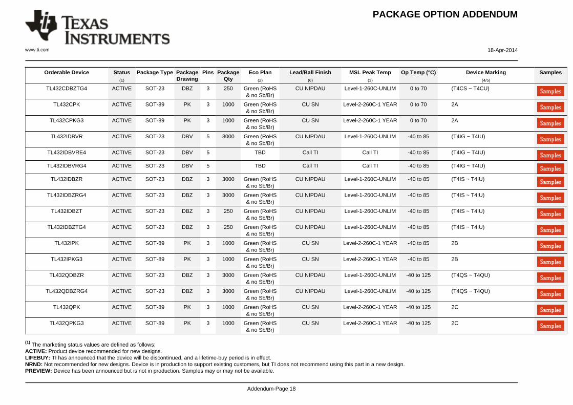
PACKAGE OPTION ADDENDUM
www.ti.com 18-Apr-2014
Addendum-Page 18
Orderable Device Status(1)
Package Type PackageDrawing
Pins PackageQty
Eco Plan(2)
Lead/Ball Finish(6)
MSL Peak Temp(3)
Op Temp (°C) Device Marking(4/5)
Samples
TL432CDBZTG4 ACTIVE SOT-23 DBZ 3 250 Green (RoHS& no Sb/Br)
CU NIPDAU Level-1-260C-UNLIM 0 to 70 (T4CS ~ T4CU)
TL432CPK ACTIVE SOT-89 PK 3 1000 Green (RoHS& no Sb/Br)
CU SN Level-2-260C-1 YEAR 0 to 70 2A
TL432CPKG3 ACTIVE SOT-89 PK 3 1000 Green (RoHS& no Sb/Br)
CU SN Level-2-260C-1 YEAR 0 to 70 2A
TL432IDBVR ACTIVE SOT-23 DBV 5 3000 Green (RoHS& no Sb/Br)
CU NIPDAU Level-1-260C-UNLIM -40 to 85 (T4IG ~ T4IU)
TL432IDBVRE4 ACTIVE SOT-23 DBV 5 TBD Call TI Call TI -40 to 85 (T4IG ~ T4IU)
TL432IDBVRG4 ACTIVE SOT-23 DBV 5 TBD Call TI Call TI -40 to 85 (T4IG ~ T4IU)
TL432IDBZR ACTIVE SOT-23 DBZ 3 3000 Green (RoHS& no Sb/Br)
CU NIPDAU Level-1-260C-UNLIM -40 to 85 (T4IS ~ T4IU)
TL432IDBZRG4 ACTIVE SOT-23 DBZ 3 3000 Green (RoHS& no Sb/Br)
CU NIPDAU Level-1-260C-UNLIM -40 to 85 (T4IS ~ T4IU)
TL432IDBZT ACTIVE SOT-23 DBZ 3 250 Green (RoHS& no Sb/Br)
CU NIPDAU Level-1-260C-UNLIM -40 to 85 (T4IS ~ T4IU)
TL432IDBZTG4 ACTIVE SOT-23 DBZ 3 250 Green (RoHS& no Sb/Br)
CU NIPDAU Level-1-260C-UNLIM -40 to 85 (T4IS ~ T4IU)
TL432IPK ACTIVE SOT-89 PK 3 1000 Green (RoHS& no Sb/Br)
CU SN Level-2-260C-1 YEAR -40 to 85 2B
TL432IPKG3 ACTIVE SOT-89 PK 3 1000 Green (RoHS& no Sb/Br)
CU SN Level-2-260C-1 YEAR -40 to 85 2B
TL432QDBZR ACTIVE SOT-23 DBZ 3 3000 Green (RoHS& no Sb/Br)
CU NIPDAU Level-1-260C-UNLIM -40 to 125 (T4QS ~ T4QU)
TL432QDBZRG4 ACTIVE SOT-23 DBZ 3 3000 Green (RoHS& no Sb/Br)
CU NIPDAU Level-1-260C-UNLIM -40 to 125 (T4QS ~ T4QU)
TL432QPK ACTIVE SOT-89 PK 3 1000 Green (RoHS& no Sb/Br)
CU SN Level-2-260C-1 YEAR -40 to 125 2C
TL432QPKG3 ACTIVE SOT-89 PK 3 1000 Green (RoHS& no Sb/Br)
CU SN Level-2-260C-1 YEAR -40 to 125 2C
(1) The marketing status values are defined as follows:ACTIVE: Product device recommended for new designs.LIFEBUY: TI has announced that the device will be discontinued, and a lifetime-buy period is in effect.NRND: Not recommended for new designs. Device is in production to support existing customers, but TI does not recommend using this part in a new design.PREVIEW: Device has been announced but is not in production. Samples may or may not be available.
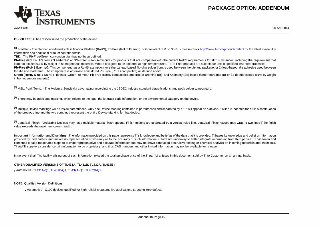
PACKAGE OPTION ADDENDUM
www.ti.com 18-Apr-2014
Addendum-Page 19
OBSOLETE: TI has discontinued the production of the device.
(2) Eco Plan - The planned eco-friendly classification: Pb-Free (RoHS), Pb-Free (RoHS Exempt), or Green (RoHS & no Sb/Br) - please check http://www.ti.com/productcontent for the latest availabilityinformation and additional product content details.TBD: The Pb-Free/Green conversion plan has not been defined.Pb-Free (RoHS): TI's terms "Lead-Free" or "Pb-Free" mean semiconductor products that are compatible with the current RoHS requirements for all 6 substances, including the requirement thatlead not exceed 0.1% by weight in homogeneous materials. Where designed to be soldered at high temperatures, TI Pb-Free products are suitable for use in specified lead-free processes.Pb-Free (RoHS Exempt): This component has a RoHS exemption for either 1) lead-based flip-chip solder bumps used between the die and package, or 2) lead-based die adhesive used betweenthe die and leadframe. The component is otherwise considered Pb-Free (RoHS compatible) as defined above.Green (RoHS & no Sb/Br): TI defines "Green" to mean Pb-Free (RoHS compatible), and free of Bromine (Br) and Antimony (Sb) based flame retardants (Br or Sb do not exceed 0.1% by weightin homogeneous material)
(3) MSL, Peak Temp. - The Moisture Sensitivity Level rating according to the JEDEC industry standard classifications, and peak solder temperature.
(4) There may be additional marking, which relates to the logo, the lot trace code information, or the environmental category on the device.
(5) Multiple Device Markings will be inside parentheses. Only one Device Marking contained in parentheses and separated by a "~" will appear on a device. If a line is indented then it is a continuationof the previous line and the two combined represent the entire Device Marking for that device.
(6) Lead/Ball Finish - Orderable Devices may have multiple material finish options. Finish options are separated by a vertical ruled line. Lead/Ball Finish values may wrap to two lines if the finishvalue exceeds the maximum column width.
Important Information and Disclaimer:The information provided on this page represents TI's knowledge and belief as of the date that it is provided. TI bases its knowledge and belief on informationprovided by third parties, and makes no representation or warranty as to the accuracy of such information. Efforts are underway to better integrate information from third parties. TI has taken andcontinues to take reasonable steps to provide representative and accurate information but may not have conducted destructive testing or chemical analysis on incoming materials and chemicals.TI and TI suppliers consider certain information to be proprietary, and thus CAS numbers and other limited information may not be available for release.
In no event shall TI's liability arising out of such information exceed the total purchase price of the TI part(s) at issue in this document sold by TI to Customer on an annual basis.
OTHER QUALIFIED VERSIONS OF TL431A, TL431B, TL432A, TL432B :
• Automotive: TL431A-Q1, TL431B-Q1, TL432A-Q1, TL432B-Q1
NOTE: Qualified Version Definitions:
• Automotive - Q100 devices qualified for high-reliability automotive applications targeting zero defects
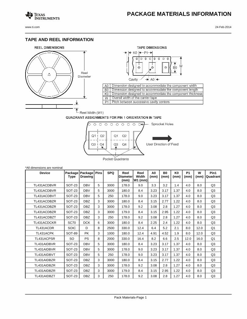
TAPE AND REEL INFORMATION
*All dimensions are nominal
Device PackageType
PackageDrawing
Pins SPQ ReelDiameter
(mm)
ReelWidth
W1 (mm)
A0(mm)
B0(mm)
K0(mm)
P1(mm)
W(mm)
Pin1Quadrant
TL431ACDBVR SOT-23 DBV 5 3000 178.0 9.0 3.3 3.2 1.4 4.0 8.0 Q3
TL431ACDBVR SOT-23 DBV 5 3000 180.0 8.4 3.23 3.17 1.37 4.0 8.0 Q3
TL431ACDBVT SOT-23 DBV 5 250 178.0 9.0 3.23 3.17 1.37 4.0 8.0 Q3
TL431ACDBZR SOT-23 DBZ 3 3000 180.0 8.4 3.15 2.77 1.22 4.0 8.0 Q3
TL431ACDBZR SOT-23 DBZ 3 3000 178.0 9.2 3.08 2.8 1.27 4.0 8.0 Q3
TL431ACDBZR SOT-23 DBZ 3 3000 179.0 8.4 3.15 2.95 1.22 4.0 8.0 Q3
TL431ACDBZT SOT-23 DBZ 3 250 178.0 9.2 3.08 2.8 1.27 4.0 8.0 Q3
TL431ACDCKR SC70 DCK 6 3000 180.0 8.4 2.25 2.4 1.22 4.0 8.0 Q3
TL431ACDR SOIC D 8 2500 330.0 12.4 6.4 5.2 2.1 8.0 12.0 Q1
TL431ACPK SOT-89 PK 3 1000 180.0 12.4 4.91 4.52 1.9 8.0 12.0 Q3
TL431ACPSR SO PS 8 2000 330.0 16.4 8.2 6.6 2.5 12.0 16.0 Q1
TL431AIDBVR SOT-23 DBV 5 3000 180.0 8.4 3.23 3.17 1.37 4.0 8.0 Q3
TL431AIDBVR SOT-23 DBV 5 3000 178.0 9.0 3.23 3.17 1.37 4.0 8.0 Q3
TL431AIDBVT SOT-23 DBV 5 250 178.0 9.0 3.23 3.17 1.37 4.0 8.0 Q3
TL431AIDBZR SOT-23 DBZ 3 3000 180.0 8.4 3.15 2.77 1.22 4.0 8.0 Q3
TL431AIDBZR SOT-23 DBZ 3 3000 178.0 9.2 3.08 2.8 1.27 4.0 8.0 Q3
TL431AIDBZR SOT-23 DBZ 3 3000 179.0 8.4 3.15 2.95 1.22 4.0 8.0 Q3
TL431AIDBZT SOT-23 DBZ 3 250 178.0 9.2 3.08 2.8 1.27 4.0 8.0 Q3
PACKAGE MATERIALS INFORMATION
www.ti.com 24-Feb-2014
Pack Materials-Page 1
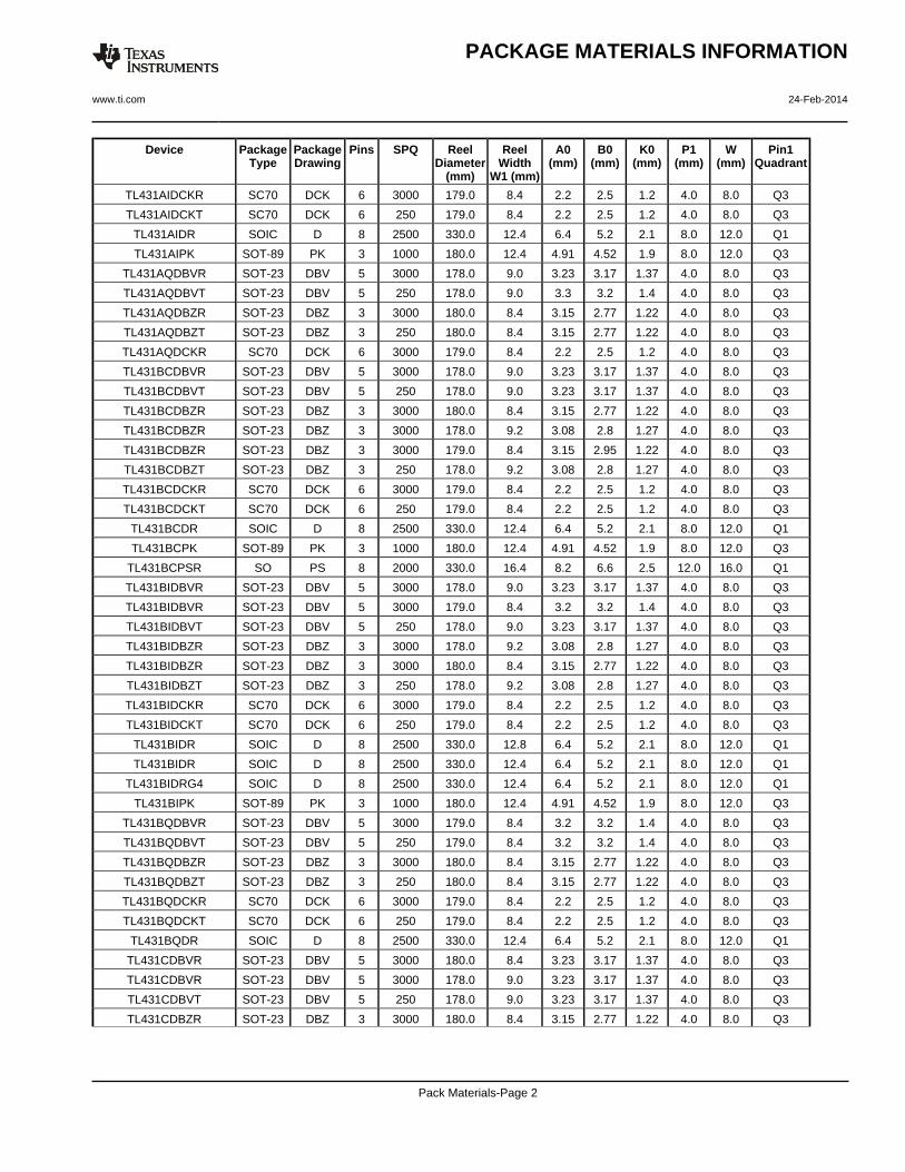
Device PackageType
PackageDrawing
Pins SPQ ReelDiameter
(mm)
ReelWidth
W1 (mm)
A0(mm)
B0(mm)
K0(mm)
P1(mm)
W(mm)
Pin1Quadrant
TL431AIDCKR SC70 DCK 6 3000 179.0 8.4 2.2 2.5 1.2 4.0 8.0 Q3
TL431AIDCKT SC70 DCK 6 250 179.0 8.4 2.2 2.5 1.2 4.0 8.0 Q3
TL431AIDR SOIC D 8 2500 330.0 12.4 6.4 5.2 2.1 8.0 12.0 Q1
TL431AIPK SOT-89 PK 3 1000 180.0 12.4 4.91 4.52 1.9 8.0 12.0 Q3
TL431AQDBVR SOT-23 DBV 5 3000 178.0 9.0 3.23 3.17 1.37 4.0 8.0 Q3
TL431AQDBVT SOT-23 DBV 5 250 178.0 9.0 3.3 3.2 1.4 4.0 8.0 Q3
TL431AQDBZR SOT-23 DBZ 3 3000 180.0 8.4 3.15 2.77 1.22 4.0 8.0 Q3
TL431AQDBZT SOT-23 DBZ 3 250 180.0 8.4 3.15 2.77 1.22 4.0 8.0 Q3
TL431AQDCKR SC70 DCK 6 3000 179.0 8.4 2.2 2.5 1.2 4.0 8.0 Q3
TL431BCDBVR SOT-23 DBV 5 3000 178.0 9.0 3.23 3.17 1.37 4.0 8.0 Q3
TL431BCDBVT SOT-23 DBV 5 250 178.0 9.0 3.23 3.17 1.37 4.0 8.0 Q3
TL431BCDBZR SOT-23 DBZ 3 3000 180.0 8.4 3.15 2.77 1.22 4.0 8.0 Q3
TL431BCDBZR SOT-23 DBZ 3 3000 178.0 9.2 3.08 2.8 1.27 4.0 8.0 Q3
TL431BCDBZR SOT-23 DBZ 3 3000 179.0 8.4 3.15 2.95 1.22 4.0 8.0 Q3
TL431BCDBZT SOT-23 DBZ 3 250 178.0 9.2 3.08 2.8 1.27 4.0 8.0 Q3
TL431BCDCKR SC70 DCK 6 3000 179.0 8.4 2.2 2.5 1.2 4.0 8.0 Q3
TL431BCDCKT SC70 DCK 6 250 179.0 8.4 2.2 2.5 1.2 4.0 8.0 Q3
TL431BCDR SOIC D 8 2500 330.0 12.4 6.4 5.2 2.1 8.0 12.0 Q1
TL431BCPK SOT-89 PK 3 1000 180.0 12.4 4.91 4.52 1.9 8.0 12.0 Q3
TL431BCPSR SO PS 8 2000 330.0 16.4 8.2 6.6 2.5 12.0 16.0 Q1
TL431BIDBVR SOT-23 DBV 5 3000 178.0 9.0 3.23 3.17 1.37 4.0 8.0 Q3
TL431BIDBVR SOT-23 DBV 5 3000 179.0 8.4 3.2 3.2 1.4 4.0 8.0 Q3
TL431BIDBVT SOT-23 DBV 5 250 178.0 9.0 3.23 3.17 1.37 4.0 8.0 Q3
TL431BIDBZR SOT-23 DBZ 3 3000 178.0 9.2 3.08 2.8 1.27 4.0 8.0 Q3
TL431BIDBZR SOT-23 DBZ 3 3000 180.0 8.4 3.15 2.77 1.22 4.0 8.0 Q3
TL431BIDBZT SOT-23 DBZ 3 250 178.0 9.2 3.08 2.8 1.27 4.0 8.0 Q3
TL431BIDCKR SC70 DCK 6 3000 179.0 8.4 2.2 2.5 1.2 4.0 8.0 Q3
TL431BIDCKT SC70 DCK 6 250 179.0 8.4 2.2 2.5 1.2 4.0 8.0 Q3
TL431BIDR SOIC D 8 2500 330.0 12.8 6.4 5.2 2.1 8.0 12.0 Q1
TL431BIDR SOIC D 8 2500 330.0 12.4 6.4 5.2 2.1 8.0 12.0 Q1
TL431BIDRG4 SOIC D 8 2500 330.0 12.4 6.4 5.2 2.1 8.0 12.0 Q1
TL431BIPK SOT-89 PK 3 1000 180.0 12.4 4.91 4.52 1.9 8.0 12.0 Q3
TL431BQDBVR SOT-23 DBV 5 3000 179.0 8.4 3.2 3.2 1.4 4.0 8.0 Q3
TL431BQDBVT SOT-23 DBV 5 250 179.0 8.4 3.2 3.2 1.4 4.0 8.0 Q3
TL431BQDBZR SOT-23 DBZ 3 3000 180.0 8.4 3.15 2.77 1.22 4.0 8.0 Q3
TL431BQDBZT SOT-23 DBZ 3 250 180.0 8.4 3.15 2.77 1.22 4.0 8.0 Q3
TL431BQDCKR SC70 DCK 6 3000 179.0 8.4 2.2 2.5 1.2 4.0 8.0 Q3
TL431BQDCKT SC70 DCK 6 250 179.0 8.4 2.2 2.5 1.2 4.0 8.0 Q3
TL431BQDR SOIC D 8 2500 330.0 12.4 6.4 5.2 2.1 8.0 12.0 Q1
TL431CDBVR SOT-23 DBV 5 3000 180.0 8.4 3.23 3.17 1.37 4.0 8.0 Q3
TL431CDBVR SOT-23 DBV 5 3000 178.0 9.0 3.23 3.17 1.37 4.0 8.0 Q3
TL431CDBVT SOT-23 DBV 5 250 178.0 9.0 3.23 3.17 1.37 4.0 8.0 Q3
TL431CDBZR SOT-23 DBZ 3 3000 180.0 8.4 3.15 2.77 1.22 4.0 8.0 Q3
PACKAGE MATERIALS INFORMATION
www.ti.com 24-Feb-2014
Pack Materials-Page 2
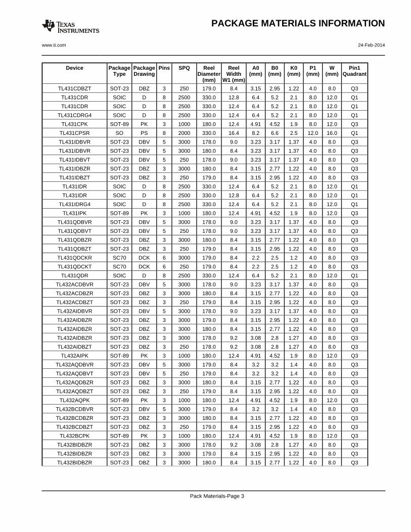
Device PackageType
PackageDrawing
Pins SPQ ReelDiameter
(mm)
ReelWidth
W1 (mm)
A0(mm)
B0(mm)
K0(mm)
P1(mm)
W(mm)
Pin1Quadrant
TL431CDBZT SOT-23 DBZ 3 250 179.0 8.4 3.15 2.95 1.22 4.0 8.0 Q3
TL431CDR SOIC D 8 2500 330.0 12.8 6.4 5.2 2.1 8.0 12.0 Q1
TL431CDR SOIC D 8 2500 330.0 12.4 6.4 5.2 2.1 8.0 12.0 Q1
TL431CDRG4 SOIC D 8 2500 330.0 12.4 6.4 5.2 2.1 8.0 12.0 Q1
TL431CPK SOT-89 PK 3 1000 180.0 12.4 4.91 4.52 1.9 8.0 12.0 Q3
TL431CPSR SO PS 8 2000 330.0 16.4 8.2 6.6 2.5 12.0 16.0 Q1
TL431IDBVR SOT-23 DBV 5 3000 178.0 9.0 3.23 3.17 1.37 4.0 8.0 Q3
TL431IDBVR SOT-23 DBV 5 3000 180.0 8.4 3.23 3.17 1.37 4.0 8.0 Q3
TL431IDBVT SOT-23 DBV 5 250 178.0 9.0 3.23 3.17 1.37 4.0 8.0 Q3
TL431IDBZR SOT-23 DBZ 3 3000 180.0 8.4 3.15 2.77 1.22 4.0 8.0 Q3
TL431IDBZT SOT-23 DBZ 3 250 179.0 8.4 3.15 2.95 1.22 4.0 8.0 Q3
TL431IDR SOIC D 8 2500 330.0 12.4 6.4 5.2 2.1 8.0 12.0 Q1
TL431IDR SOIC D 8 2500 330.0 12.8 6.4 5.2 2.1 8.0 12.0 Q1
TL431IDRG4 SOIC D 8 2500 330.0 12.4 6.4 5.2 2.1 8.0 12.0 Q1
TL431IPK SOT-89 PK 3 1000 180.0 12.4 4.91 4.52 1.9 8.0 12.0 Q3
TL431QDBVR SOT-23 DBV 5 3000 178.0 9.0 3.23 3.17 1.37 4.0 8.0 Q3
TL431QDBVT SOT-23 DBV 5 250 178.0 9.0 3.23 3.17 1.37 4.0 8.0 Q3
TL431QDBZR SOT-23 DBZ 3 3000 180.0 8.4 3.15 2.77 1.22 4.0 8.0 Q3
TL431QDBZT SOT-23 DBZ 3 250 179.0 8.4 3.15 2.95 1.22 4.0 8.0 Q3
TL431QDCKR SC70 DCK 6 3000 179.0 8.4 2.2 2.5 1.2 4.0 8.0 Q3
TL431QDCKT SC70 DCK 6 250 179.0 8.4 2.2 2.5 1.2 4.0 8.0 Q3
TL431QDR SOIC D 8 2500 330.0 12.4 6.4 5.2 2.1 8.0 12.0 Q1
TL432ACDBVR SOT-23 DBV 5 3000 178.0 9.0 3.23 3.17 1.37 4.0 8.0 Q3
TL432ACDBZR SOT-23 DBZ 3 3000 180.0 8.4 3.15 2.77 1.22 4.0 8.0 Q3
TL432ACDBZT SOT-23 DBZ 3 250 179.0 8.4 3.15 2.95 1.22 4.0 8.0 Q3
TL432AIDBVR SOT-23 DBV 5 3000 178.0 9.0 3.23 3.17 1.37 4.0 8.0 Q3
TL432AIDBZR SOT-23 DBZ 3 3000 179.0 8.4 3.15 2.95 1.22 4.0 8.0 Q3
TL432AIDBZR SOT-23 DBZ 3 3000 180.0 8.4 3.15 2.77 1.22 4.0 8.0 Q3
TL432AIDBZR SOT-23 DBZ 3 3000 178.0 9.2 3.08 2.8 1.27 4.0 8.0 Q3
TL432AIDBZT SOT-23 DBZ 3 250 178.0 9.2 3.08 2.8 1.27 4.0 8.0 Q3
TL432AIPK SOT-89 PK 3 1000 180.0 12.4 4.91 4.52 1.9 8.0 12.0 Q3
TL432AQDBVR SOT-23 DBV 5 3000 179.0 8.4 3.2 3.2 1.4 4.0 8.0 Q3
TL432AQDBVT SOT-23 DBV 5 250 179.0 8.4 3.2 3.2 1.4 4.0 8.0 Q3
TL432AQDBZR SOT-23 DBZ 3 3000 180.0 8.4 3.15 2.77 1.22 4.0 8.0 Q3
TL432AQDBZT SOT-23 DBZ 3 250 179.0 8.4 3.15 2.95 1.22 4.0 8.0 Q3
TL432AQPK SOT-89 PK 3 1000 180.0 12.4 4.91 4.52 1.9 8.0 12.0 Q3
TL432BCDBVR SOT-23 DBV 5 3000 179.0 8.4 3.2 3.2 1.4 4.0 8.0 Q3
TL432BCDBZR SOT-23 DBZ 3 3000 180.0 8.4 3.15 2.77 1.22 4.0 8.0 Q3
TL432BCDBZT SOT-23 DBZ 3 250 179.0 8.4 3.15 2.95 1.22 4.0 8.0 Q3
TL432BCPK SOT-89 PK 3 1000 180.0 12.4 4.91 4.52 1.9 8.0 12.0 Q3
TL432BIDBZR SOT-23 DBZ 3 3000 178.0 9.2 3.08 2.8 1.27 4.0 8.0 Q3
TL432BIDBZR SOT-23 DBZ 3 3000 179.0 8.4 3.15 2.95 1.22 4.0 8.0 Q3
TL432BIDBZR SOT-23 DBZ 3 3000 180.0 8.4 3.15 2.77 1.22 4.0 8.0 Q3
PACKAGE MATERIALS INFORMATION
www.ti.com 24-Feb-2014
Pack Materials-Page 3
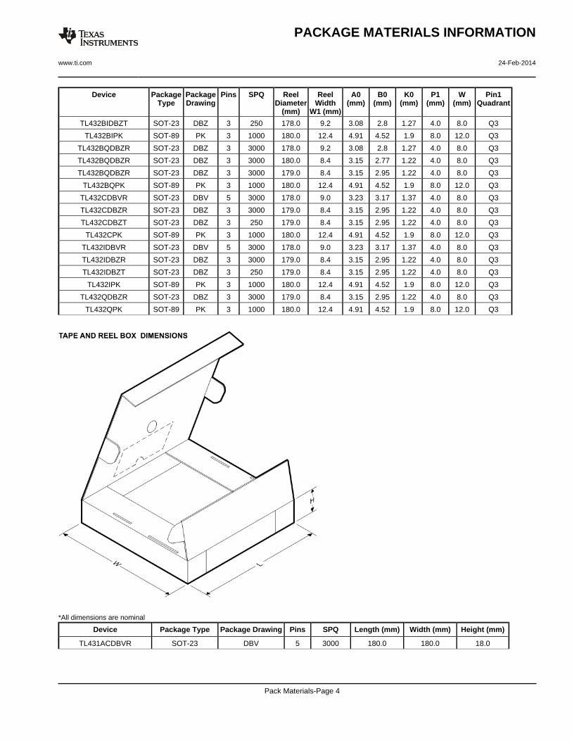
Device PackageType
PackageDrawing
Pins SPQ ReelDiameter
(mm)
ReelWidth
W1 (mm)
A0(mm)
B0(mm)
K0(mm)
P1(mm)
W(mm)
Pin1Quadrant
TL432BIDBZT SOT-23 DBZ 3 250 178.0 9.2 3.08 2.8 1.27 4.0 8.0 Q3
TL432BIPK SOT-89 PK 3 1000 180.0 12.4 4.91 4.52 1.9 8.0 12.0 Q3
TL432BQDBZR SOT-23 DBZ 3 3000 178.0 9.2 3.08 2.8 1.27 4.0 8.0 Q3
TL432BQDBZR SOT-23 DBZ 3 3000 180.0 8.4 3.15 2.77 1.22 4.0 8.0 Q3
TL432BQDBZR SOT-23 DBZ 3 3000 179.0 8.4 3.15 2.95 1.22 4.0 8.0 Q3
TL432BQPK SOT-89 PK 3 1000 180.0 12.4 4.91 4.52 1.9 8.0 12.0 Q3
TL432CDBVR SOT-23 DBV 5 3000 178.0 9.0 3.23 3.17 1.37 4.0 8.0 Q3
TL432CDBZR SOT-23 DBZ 3 3000 179.0 8.4 3.15 2.95 1.22 4.0 8.0 Q3
TL432CDBZT SOT-23 DBZ 3 250 179.0 8.4 3.15 2.95 1.22 4.0 8.0 Q3
TL432CPK SOT-89 PK 3 1000 180.0 12.4 4.91 4.52 1.9 8.0 12.0 Q3
TL432IDBVR SOT-23 DBV 5 3000 178.0 9.0 3.23 3.17 1.37 4.0 8.0 Q3
TL432IDBZR SOT-23 DBZ 3 3000 179.0 8.4 3.15 2.95 1.22 4.0 8.0 Q3
TL432IDBZT SOT-23 DBZ 3 250 179.0 8.4 3.15 2.95 1.22 4.0 8.0 Q3
TL432IPK SOT-89 PK 3 1000 180.0 12.4 4.91 4.52 1.9 8.0 12.0 Q3
TL432QDBZR SOT-23 DBZ 3 3000 179.0 8.4 3.15 2.95 1.22 4.0 8.0 Q3
TL432QPK SOT-89 PK 3 1000 180.0 12.4 4.91 4.52 1.9 8.0 12.0 Q3
*All dimensions are nominal
Device Package Type Package Drawing Pins SPQ Length (mm) Width (mm) Height (mm)
TL431ACDBVR SOT-23 DBV 5 3000 180.0 180.0 18.0
PACKAGE MATERIALS INFORMATION
www.ti.com 24-Feb-2014
Pack Materials-Page 4
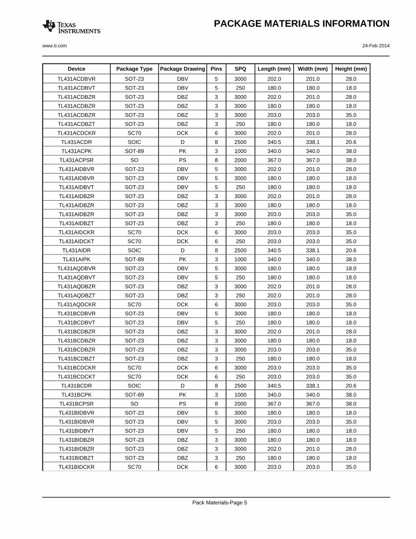
Device Package Type Package Drawing Pins SPQ Length (mm) Width (mm) Height (mm)
TL431ACDBVR SOT-23 DBV 5 3000 202.0 201.0 28.0
TL431ACDBVT SOT-23 DBV 5 250 180.0 180.0 18.0
TL431ACDBZR SOT-23 DBZ 3 3000 202.0 201.0 28.0
TL431ACDBZR SOT-23 DBZ 3 3000 180.0 180.0 18.0
TL431ACDBZR SOT-23 DBZ 3 3000 203.0 203.0 35.0
TL431ACDBZT SOT-23 DBZ 3 250 180.0 180.0 18.0
TL431ACDCKR SC70 DCK 6 3000 202.0 201.0 28.0
TL431ACDR SOIC D 8 2500 340.5 338.1 20.6
TL431ACPK SOT-89 PK 3 1000 340.0 340.0 38.0
TL431ACPSR SO PS 8 2000 367.0 367.0 38.0
TL431AIDBVR SOT-23 DBV 5 3000 202.0 201.0 28.0
TL431AIDBVR SOT-23 DBV 5 3000 180.0 180.0 18.0
TL431AIDBVT SOT-23 DBV 5 250 180.0 180.0 18.0
TL431AIDBZR SOT-23 DBZ 3 3000 202.0 201.0 28.0
TL431AIDBZR SOT-23 DBZ 3 3000 180.0 180.0 18.0
TL431AIDBZR SOT-23 DBZ 3 3000 203.0 203.0 35.0
TL431AIDBZT SOT-23 DBZ 3 250 180.0 180.0 18.0
TL431AIDCKR SC70 DCK 6 3000 203.0 203.0 35.0
TL431AIDCKT SC70 DCK 6 250 203.0 203.0 35.0
TL431AIDR SOIC D 8 2500 340.5 338.1 20.6
TL431AIPK SOT-89 PK 3 1000 340.0 340.0 38.0
TL431AQDBVR SOT-23 DBV 5 3000 180.0 180.0 18.0
TL431AQDBVT SOT-23 DBV 5 250 180.0 180.0 18.0
TL431AQDBZR SOT-23 DBZ 3 3000 202.0 201.0 28.0
TL431AQDBZT SOT-23 DBZ 3 250 202.0 201.0 28.0
TL431AQDCKR SC70 DCK 6 3000 203.0 203.0 35.0
TL431BCDBVR SOT-23 DBV 5 3000 180.0 180.0 18.0
TL431BCDBVT SOT-23 DBV 5 250 180.0 180.0 18.0
TL431BCDBZR SOT-23 DBZ 3 3000 202.0 201.0 28.0
TL431BCDBZR SOT-23 DBZ 3 3000 180.0 180.0 18.0
TL431BCDBZR SOT-23 DBZ 3 3000 203.0 203.0 35.0
TL431BCDBZT SOT-23 DBZ 3 250 180.0 180.0 18.0
TL431BCDCKR SC70 DCK 6 3000 203.0 203.0 35.0
TL431BCDCKT SC70 DCK 6 250 203.0 203.0 35.0
TL431BCDR SOIC D 8 2500 340.5 338.1 20.6
TL431BCPK SOT-89 PK 3 1000 340.0 340.0 38.0
TL431BCPSR SO PS 8 2000 367.0 367.0 38.0
TL431BIDBVR SOT-23 DBV 5 3000 180.0 180.0 18.0
TL431BIDBVR SOT-23 DBV 5 3000 203.0 203.0 35.0
TL431BIDBVT SOT-23 DBV 5 250 180.0 180.0 18.0
TL431BIDBZR SOT-23 DBZ 3 3000 180.0 180.0 18.0
TL431BIDBZR SOT-23 DBZ 3 3000 202.0 201.0 28.0
TL431BIDBZT SOT-23 DBZ 3 250 180.0 180.0 18.0
TL431BIDCKR SC70 DCK 6 3000 203.0 203.0 35.0
PACKAGE MATERIALS INFORMATION
www.ti.com 24-Feb-2014
Pack Materials-Page 5
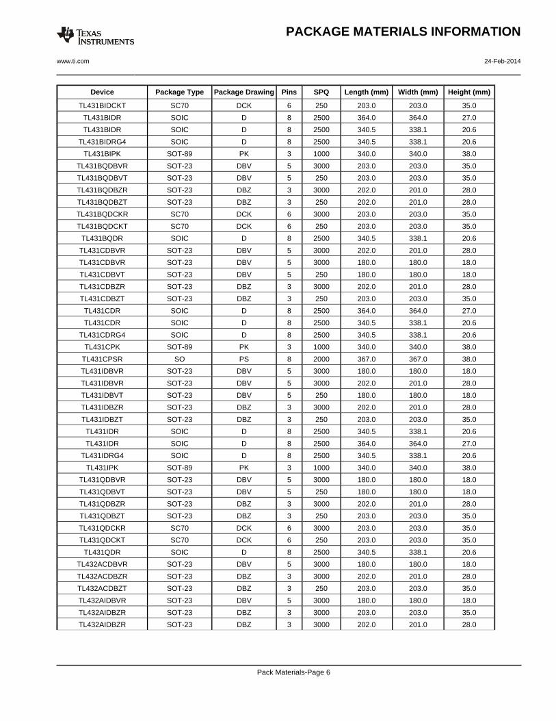
Device Package Type Package Drawing Pins SPQ Length (mm) Width (mm) Height (mm)
TL431BIDCKT SC70 DCK 6 250 203.0 203.0 35.0
TL431BIDR SOIC D 8 2500 364.0 364.0 27.0
TL431BIDR SOIC D 8 2500 340.5 338.1 20.6
TL431BIDRG4 SOIC D 8 2500 340.5 338.1 20.6
TL431BIPK SOT-89 PK 3 1000 340.0 340.0 38.0
TL431BQDBVR SOT-23 DBV 5 3000 203.0 203.0 35.0
TL431BQDBVT SOT-23 DBV 5 250 203.0 203.0 35.0
TL431BQDBZR SOT-23 DBZ 3 3000 202.0 201.0 28.0
TL431BQDBZT SOT-23 DBZ 3 250 202.0 201.0 28.0
TL431BQDCKR SC70 DCK 6 3000 203.0 203.0 35.0
TL431BQDCKT SC70 DCK 6 250 203.0 203.0 35.0
TL431BQDR SOIC D 8 2500 340.5 338.1 20.6
TL431CDBVR SOT-23 DBV 5 3000 202.0 201.0 28.0
TL431CDBVR SOT-23 DBV 5 3000 180.0 180.0 18.0
TL431CDBVT SOT-23 DBV 5 250 180.0 180.0 18.0
TL431CDBZR SOT-23 DBZ 3 3000 202.0 201.0 28.0
TL431CDBZT SOT-23 DBZ 3 250 203.0 203.0 35.0
TL431CDR SOIC D 8 2500 364.0 364.0 27.0
TL431CDR SOIC D 8 2500 340.5 338.1 20.6
TL431CDRG4 SOIC D 8 2500 340.5 338.1 20.6
TL431CPK SOT-89 PK 3 1000 340.0 340.0 38.0
TL431CPSR SO PS 8 2000 367.0 367.0 38.0
TL431IDBVR SOT-23 DBV 5 3000 180.0 180.0 18.0
TL431IDBVR SOT-23 DBV 5 3000 202.0 201.0 28.0
TL431IDBVT SOT-23 DBV 5 250 180.0 180.0 18.0
TL431IDBZR SOT-23 DBZ 3 3000 202.0 201.0 28.0
TL431IDBZT SOT-23 DBZ 3 250 203.0 203.0 35.0
TL431IDR SOIC D 8 2500 340.5 338.1 20.6
TL431IDR SOIC D 8 2500 364.0 364.0 27.0
TL431IDRG4 SOIC D 8 2500 340.5 338.1 20.6
TL431IPK SOT-89 PK 3 1000 340.0 340.0 38.0
TL431QDBVR SOT-23 DBV 5 3000 180.0 180.0 18.0
TL431QDBVT SOT-23 DBV 5 250 180.0 180.0 18.0
TL431QDBZR SOT-23 DBZ 3 3000 202.0 201.0 28.0
TL431QDBZT SOT-23 DBZ 3 250 203.0 203.0 35.0
TL431QDCKR SC70 DCK 6 3000 203.0 203.0 35.0
TL431QDCKT SC70 DCK 6 250 203.0 203.0 35.0
TL431QDR SOIC D 8 2500 340.5 338.1 20.6
TL432ACDBVR SOT-23 DBV 5 3000 180.0 180.0 18.0
TL432ACDBZR SOT-23 DBZ 3 3000 202.0 201.0 28.0
TL432ACDBZT SOT-23 DBZ 3 250 203.0 203.0 35.0
TL432AIDBVR SOT-23 DBV 5 3000 180.0 180.0 18.0
TL432AIDBZR SOT-23 DBZ 3 3000 203.0 203.0 35.0
TL432AIDBZR SOT-23 DBZ 3 3000 202.0 201.0 28.0
PACKAGE MATERIALS INFORMATION
www.ti.com 24-Feb-2014
Pack Materials-Page 6
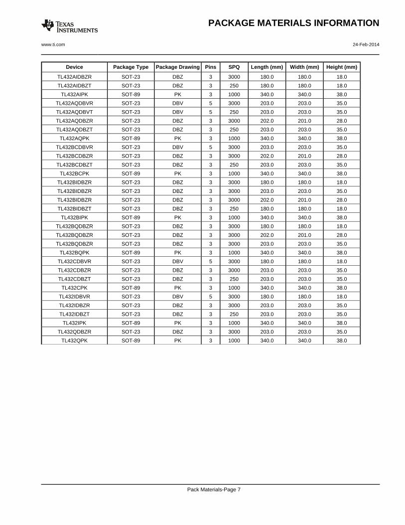
Device Package Type Package Drawing Pins SPQ Length (mm) Width (mm) Height (mm)
TL432AIDBZR SOT-23 DBZ 3 3000 180.0 180.0 18.0
TL432AIDBZT SOT-23 DBZ 3 250 180.0 180.0 18.0
TL432AIPK SOT-89 PK 3 1000 340.0 340.0 38.0
TL432AQDBVR SOT-23 DBV 5 3000 203.0 203.0 35.0
TL432AQDBVT SOT-23 DBV 5 250 203.0 203.0 35.0
TL432AQDBZR SOT-23 DBZ 3 3000 202.0 201.0 28.0
TL432AQDBZT SOT-23 DBZ 3 250 203.0 203.0 35.0
TL432AQPK SOT-89 PK 3 1000 340.0 340.0 38.0
TL432BCDBVR SOT-23 DBV 5 3000 203.0 203.0 35.0
TL432BCDBZR SOT-23 DBZ 3 3000 202.0 201.0 28.0
TL432BCDBZT SOT-23 DBZ 3 250 203.0 203.0 35.0
TL432BCPK SOT-89 PK 3 1000 340.0 340.0 38.0
TL432BIDBZR SOT-23 DBZ 3 3000 180.0 180.0 18.0
TL432BIDBZR SOT-23 DBZ 3 3000 203.0 203.0 35.0
TL432BIDBZR SOT-23 DBZ 3 3000 202.0 201.0 28.0
TL432BIDBZT SOT-23 DBZ 3 250 180.0 180.0 18.0
TL432BIPK SOT-89 PK 3 1000 340.0 340.0 38.0
TL432BQDBZR SOT-23 DBZ 3 3000 180.0 180.0 18.0
TL432BQDBZR SOT-23 DBZ 3 3000 202.0 201.0 28.0
TL432BQDBZR SOT-23 DBZ 3 3000 203.0 203.0 35.0
TL432BQPK SOT-89 PK 3 1000 340.0 340.0 38.0
TL432CDBVR SOT-23 DBV 5 3000 180.0 180.0 18.0
TL432CDBZR SOT-23 DBZ 3 3000 203.0 203.0 35.0
TL432CDBZT SOT-23 DBZ 3 250 203.0 203.0 35.0
TL432CPK SOT-89 PK 3 1000 340.0 340.0 38.0
TL432IDBVR SOT-23 DBV 5 3000 180.0 180.0 18.0
TL432IDBZR SOT-23 DBZ 3 3000 203.0 203.0 35.0
TL432IDBZT SOT-23 DBZ 3 250 203.0 203.0 35.0
TL432IPK SOT-89 PK 3 1000 340.0 340.0 38.0
TL432QDBZR SOT-23 DBZ 3 3000 203.0 203.0 35.0
TL432QPK SOT-89 PK 3 1000 340.0 340.0 38.0
PACKAGE MATERIALS INFORMATION
www.ti.com 24-Feb-2014
Pack Materials-Page 7
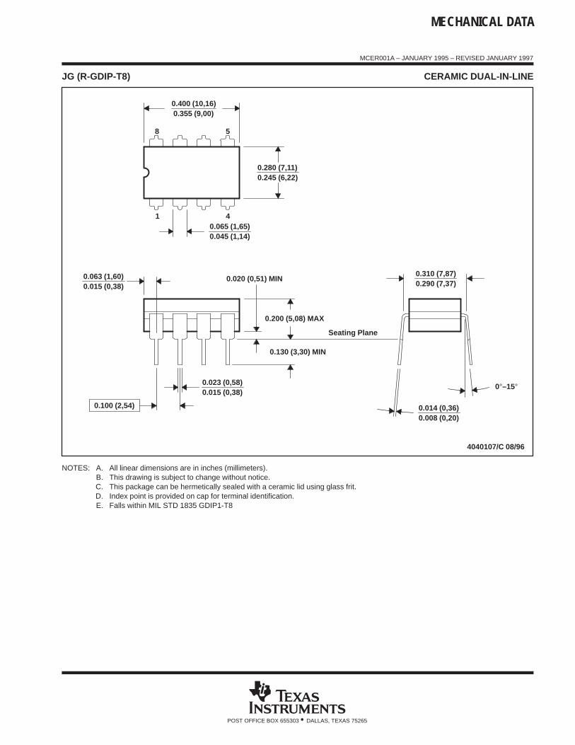
MECHANICAL DATA
MCER001A – JANUARY 1995 – REVISED JANUARY 1997
POST OFFICE BOX 655303 • DALLAS, TEXAS 75265
JG (R-GDIP-T8) CERAMIC DUAL-IN-LINE
0.310 (7,87)0.290 (7,37)
0.014 (0,36)0.008 (0,20)
Seating Plane
4040107/C 08/96
5
40.065 (1,65)0.045 (1,14)
8
1
0.020 (0,51) MIN
0.400 (10,16)0.355 (9,00)
0.015 (0,38)0.023 (0,58)
0.063 (1,60)0.015 (0,38)
0.200 (5,08) MAX
0.130 (3,30) MIN
0.245 (6,22)0.280 (7,11)
0.100 (2,54)
0°–15°
NOTES: A. All linear dimensions are in inches (millimeters).B. This drawing is subject to change without notice.C. This package can be hermetically sealed with a ceramic lid using glass frit.D. Index point is provided on cap for terminal identification.E. Falls within MIL STD 1835 GDIP1-T8
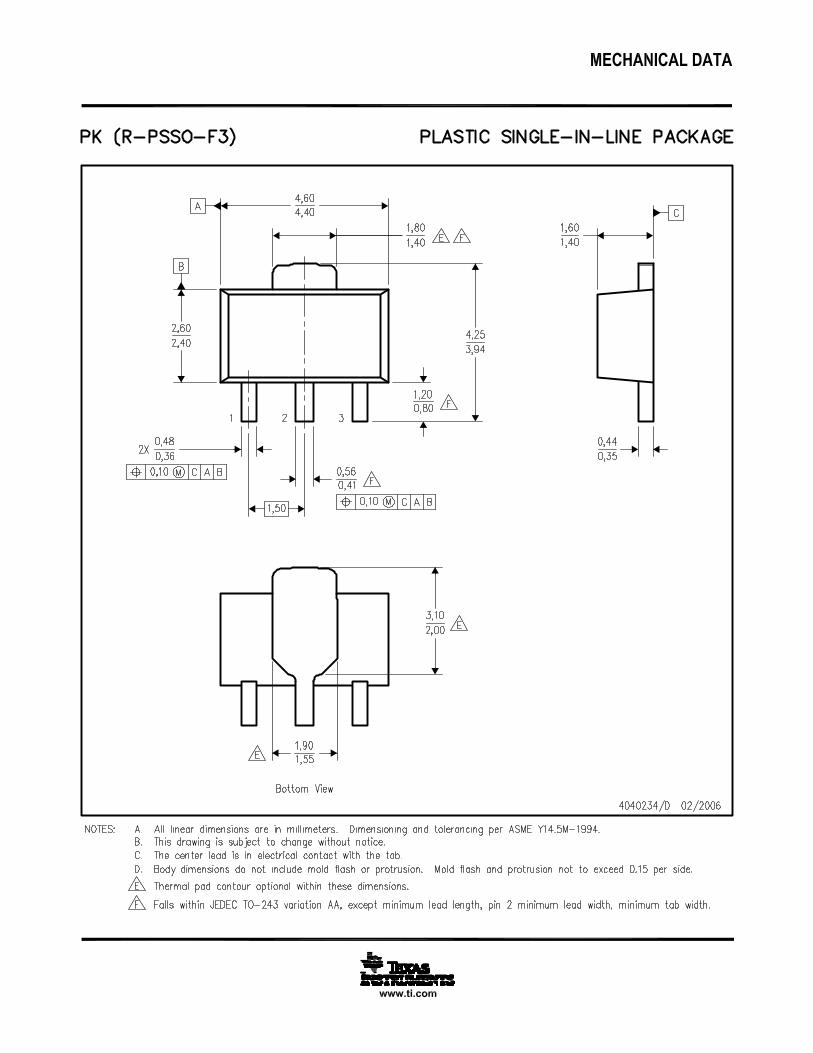
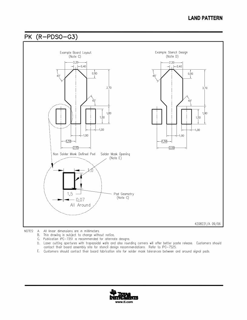
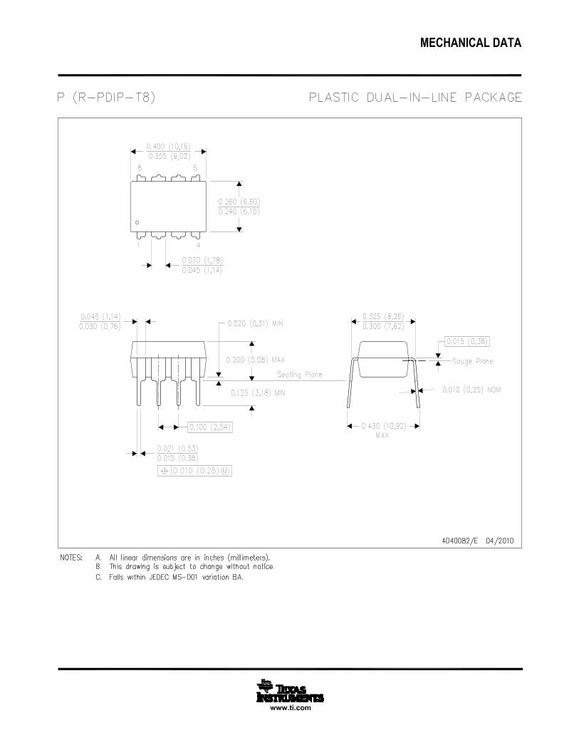
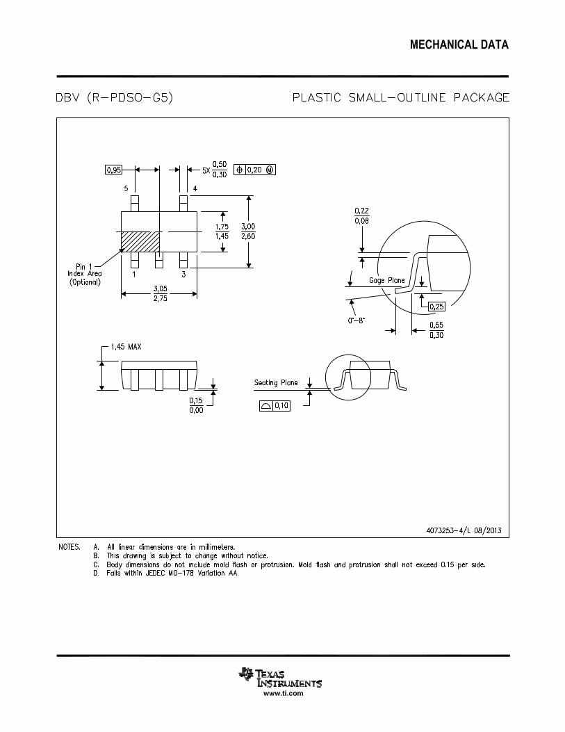
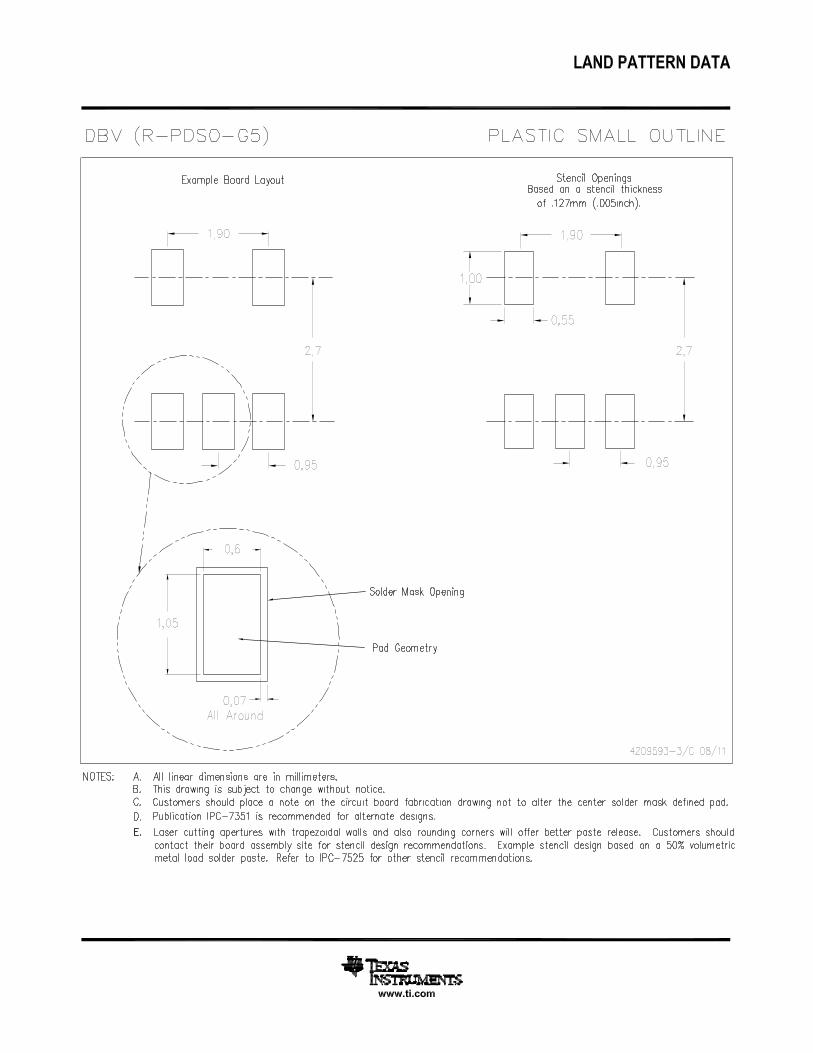
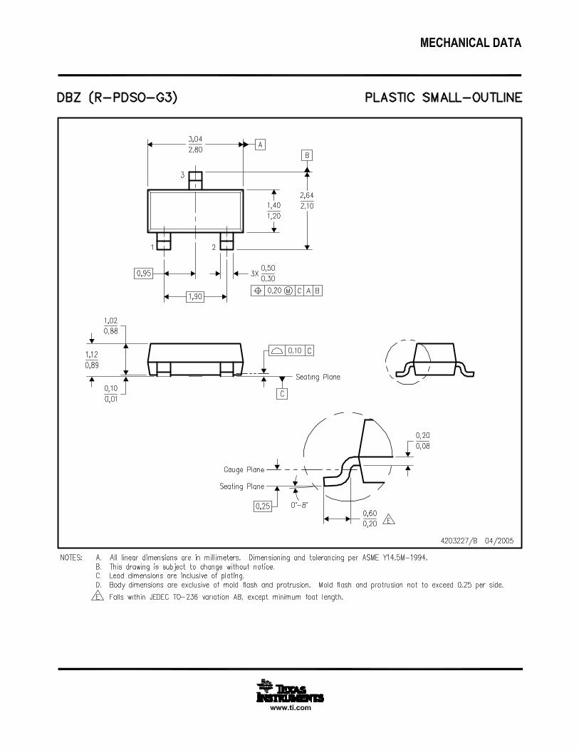
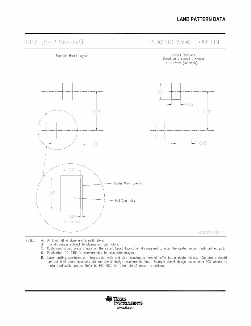
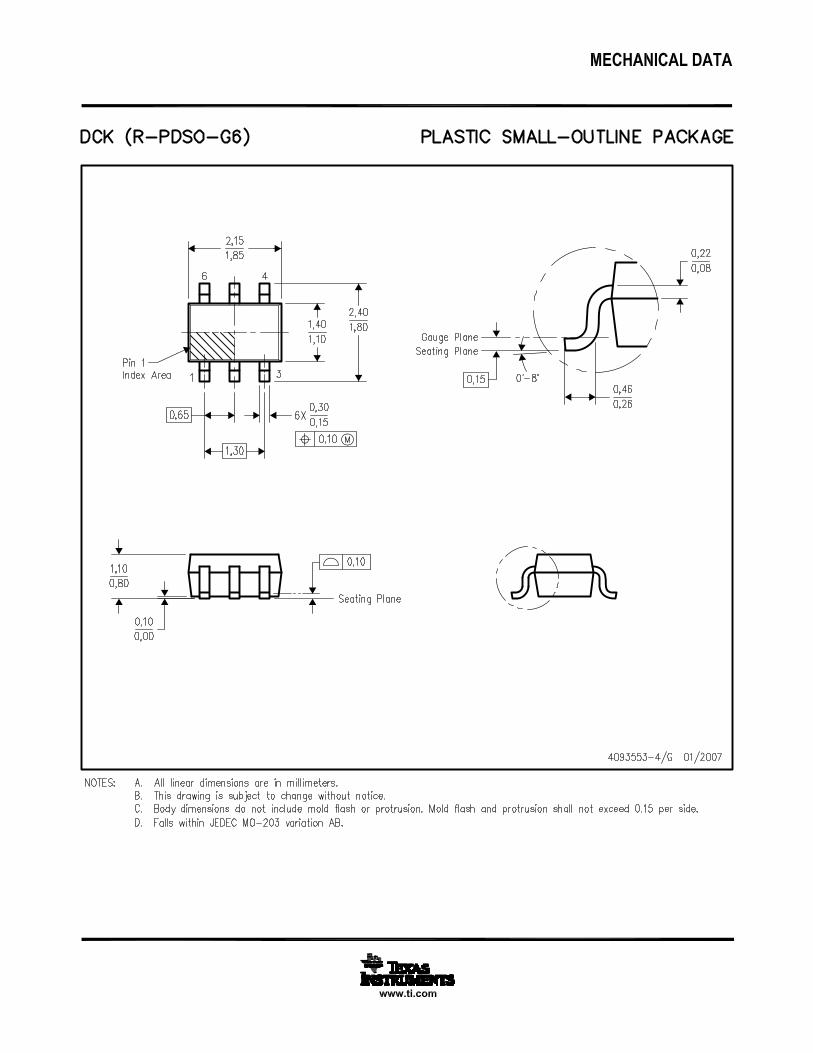

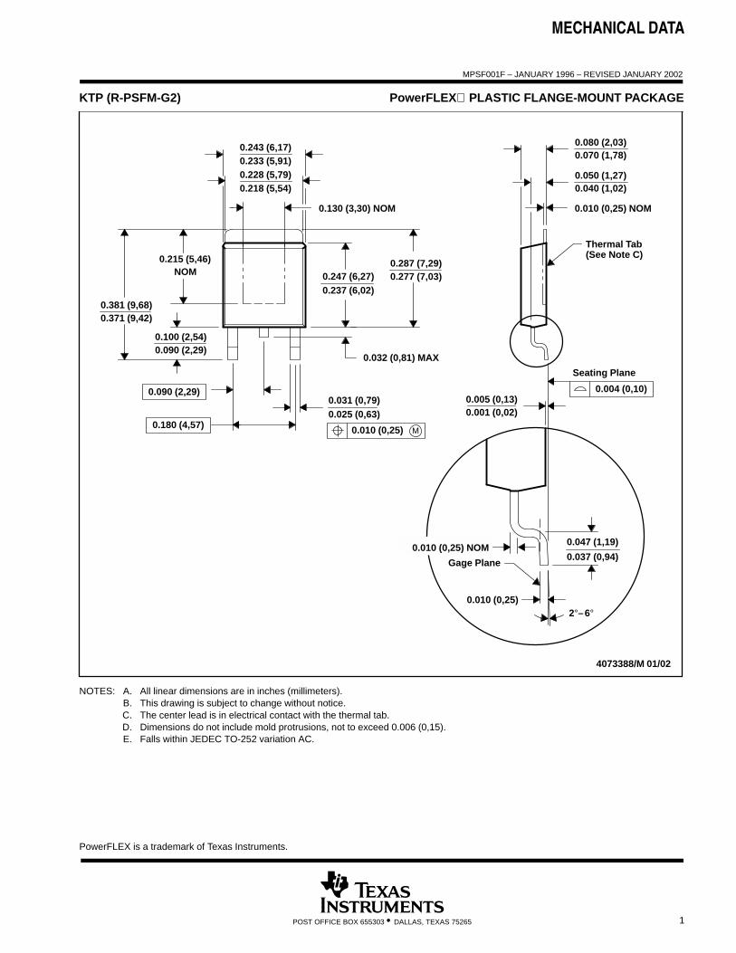
MECHANICAL DATA
MPSF001F – JANUARY 1996 – REVISED JANUARY 2002
1POST OFFICE BOX 655303 • DALLAS, TEXAS 75265
KTP (R-PSFM-G2) PowerFLEX PLASTIC FLANGE-MOUNT PACKAGE
0.228 (5,79)0.218 (5,54)
0.233 (5,91)0.243 (6,17)
0.001 (0,02)0.005 (0,13)
0.070 (1,78)
Seating Plane
0.080 (2,03)
0.010 (0,25) NOM
Gage Plane
0.010 (0,25)
4073388/M 01/02
0.037 (0,94)
0.047 (1,19)
0.247 (6,27)0.237 (6,02)
NOM0.215 (5,46)
0.371 (9,42)0.381 (9,68)
0.090 (2,29)0.100 (2,54)
0.287 (7,29)
0.031 (0,79)
0.032 (0,81) MAX
0.277 (7,03)
0.025 (0,63)
0.130 (3,30) NOM
0.090 (2,29)
0.180 (4,57)M0.010 (0,25)
0.004 (0,10)
2°–6°
0.040 (1,02)0.050 (1,27)
Thermal Tab(See Note C)
0.010 (0,25) NOM
NOTES: A. All linear dimensions are in inches (millimeters).B. This drawing is subject to change without notice.C. The center lead is in electrical contact with the thermal tab.D. Dimensions do not include mold protrusions, not to exceed 0.006 (0,15).E. Falls within JEDEC TO-252 variation AC.
PowerFLEX is a trademark of Texas Instruments.
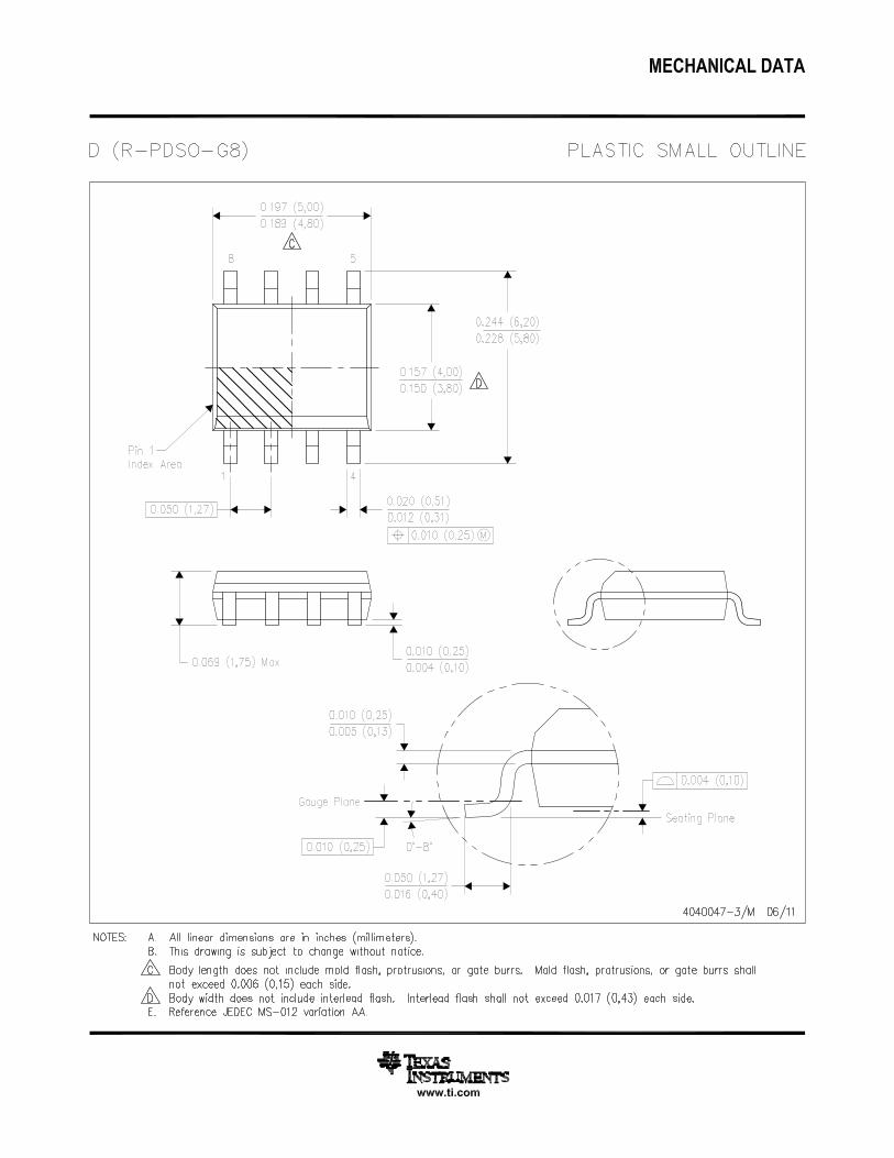
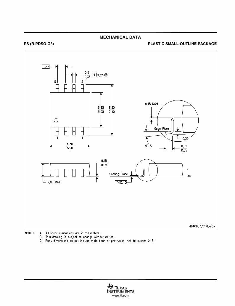
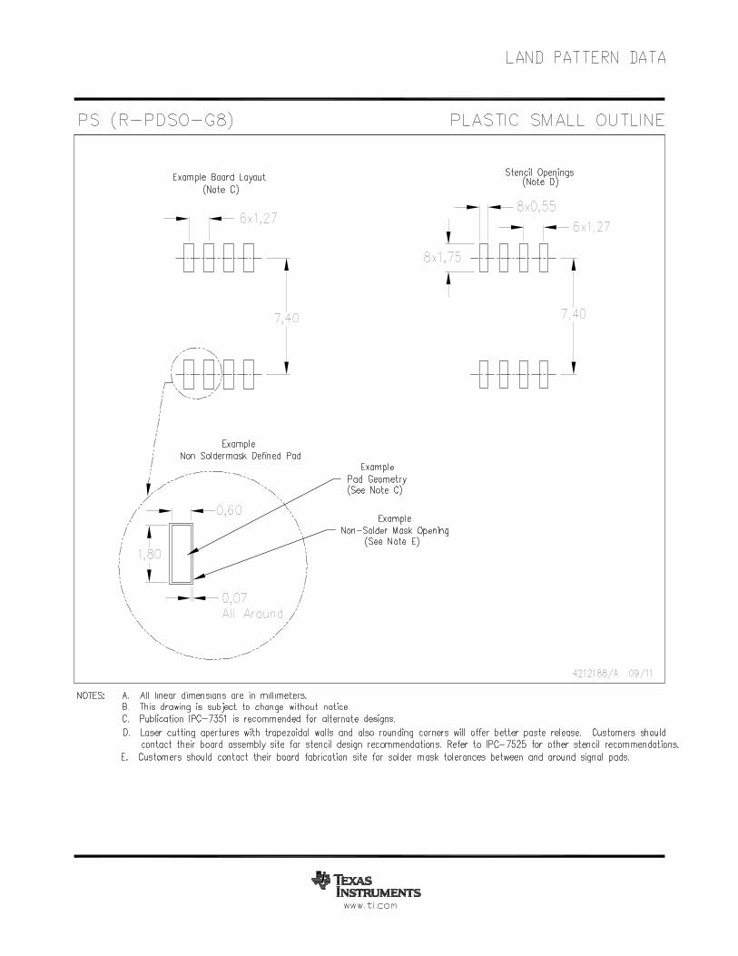
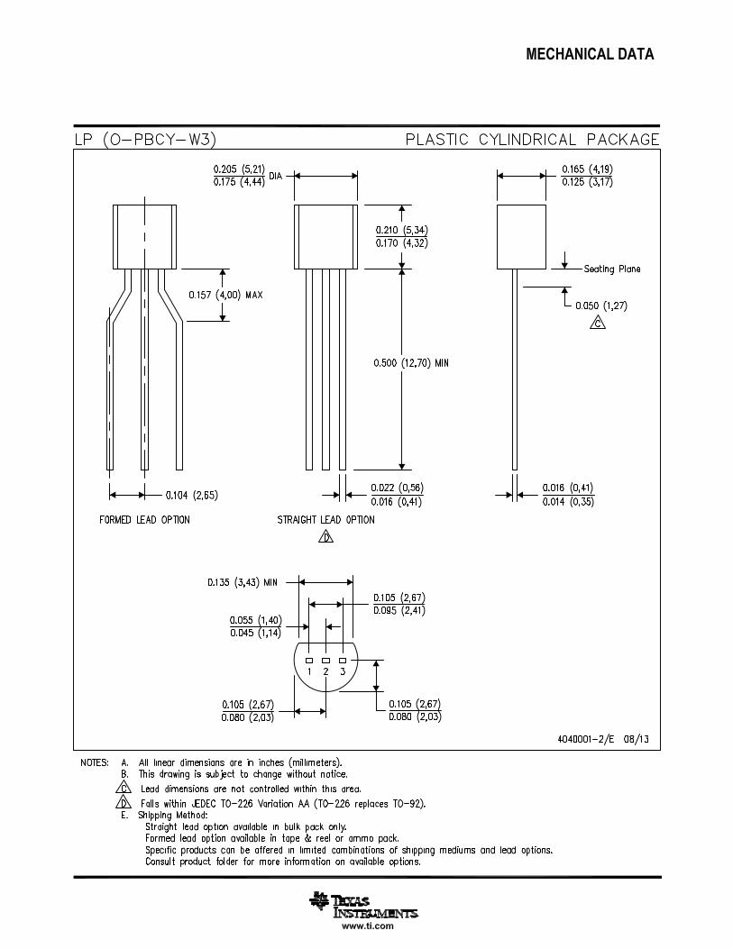
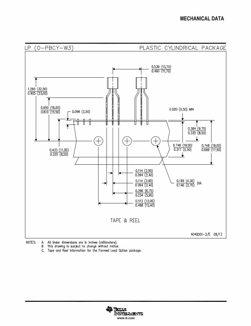
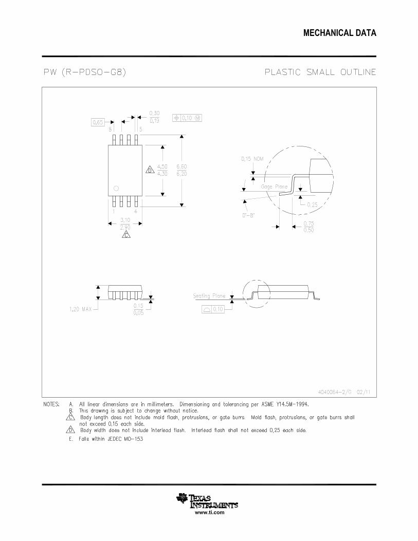
IMPORTANT NOTICETexas Instruments Incorporated and its subsidiaries (TI) reserve the right to make corrections, enhancements, improvements and otherchanges to its semiconductor products and services per JESD46, latest issue, and to discontinue any product or service per JESD48, latestissue. Buyers should obtain the latest relevant information before placing orders and should verify that such information is current andcomplete. All semiconductor products (also referred to herein as “components”) are sold subject to TI’s terms and conditions of salesupplied at the time of order acknowledgment.TI warrants performance of its components to the specifications applicable at the time of sale, in accordance with the warranty in TI’s termsand conditions of sale of semiconductor products. Testing and other quality control techniques are used to the extent TI deems necessaryto support this warranty. Except where mandated by applicable law, testing of all parameters of each component is not necessarilyperformed.TI assumes no liability for applications assistance or the design of Buyers’ products. Buyers are responsible for their products andapplications using TI components. To minimize the risks associated with Buyers’ products and applications, Buyers should provideadequate design and operating safeguards.TI does not warrant or represent that any license, either express or implied, is granted under any patent right, copyright, mask work right, orother intellectual property right relating to any combination, machine, or process in which TI components or services are used. Informationpublished by TI regarding third-party products or services does not constitute a license to use such products or services or a warranty orendorsement thereof. Use of such information may require a license from a third party under the patents or other intellectual property of thethird party, or a license from TI under the patents or other intellectual property of TI.Reproduction of significant portions of TI information in TI data books or data sheets is permissible only if reproduction is without alterationand is accompanied by all associated warranties, conditions, limitations, and notices. TI is not responsible or liable for such altereddocumentation. Information of third parties may be subject to additional restrictions.Resale of TI components or services with statements different from or beyond the parameters stated by TI for that component or servicevoids all express and any implied warranties for the associated TI component or service and is an unfair and deceptive business practice.TI is not responsible or liable for any such statements.Buyer acknowledges and agrees that it is solely responsible for compliance with all legal, regulatory and safety-related requirementsconcerning its products, and any use of TI components in its applications, notwithstanding any applications-related information or supportthat may be provided by TI. Buyer represents and agrees that it has all the necessary expertise to create and implement safeguards whichanticipate dangerous consequences of failures, monitor failures and their consequences, lessen the likelihood of failures that might causeharm and take appropriate remedial actions. Buyer will fully indemnify TI and its representatives against any damages arising out of the useof any TI components in safety-critical applications.In some cases, TI components may be promoted specifically to facilitate safety-related applications. With such components, TI’s goal is tohelp enable customers to design and create their own end-product solutions that meet applicable functional safety standards andrequirements. Nonetheless, such components are subject to these terms.No TI components are authorized for use in FDA Class III (or similar life-critical medical equipment) unless authorized officers of the partieshave executed a special agreement specifically governing such use.Only those TI components which TI has specifically designated as military grade or “enhanced plastic” are designed and intended for use inmilitary/aerospace applications or environments. Buyer acknowledges and agrees that any military or aerospace use of TI componentswhich have not been so designated is solely at the Buyer's risk, and that Buyer is solely responsible for compliance with all legal andregulatory requirements in connection with such use.TI has specifically designated certain components as meeting ISO/TS16949 requirements, mainly for automotive use. In any case of use ofnon-designated products, TI will not be responsible for any failure to meet ISO/TS16949.Products ApplicationsAudio www.ti.com/audio Automotive and Transportation www.ti.com/automotiveAmplifiers amplifier.ti.com Communications and Telecom www.ti.com/communicationsData Converters dataconverter.ti.com Computers and Peripherals www.ti.com/computersDLP® Products www.dlp.com Consumer Electronics www.ti.com/consumer-appsDSP dsp.ti.com Energy and Lighting www.ti.com/energyClocks and Timers www.ti.com/clocks Industrial www.ti.com/industrialInterface interface.ti.com Medical www.ti.com/medicalLogic logic.ti.com Security www.ti.com/securityPower Mgmt power.ti.com Space, Avionics and Defense www.ti.com/space-avionics-defenseMicrocontrollers microcontroller.ti.com Video and Imaging www.ti.com/videoRFID www.ti-rfid.comOMAP Applications Processors www.ti.com/omap TI E2E Community e2e.ti.comWireless Connectivity www.ti.com/wirelessconnectivity
Mailing Address: Texas Instruments, Post Office Box 655303, Dallas, Texas 75265Copyright © 2014, Texas Instruments Incorporated