Embed Size (px)
Citation preview
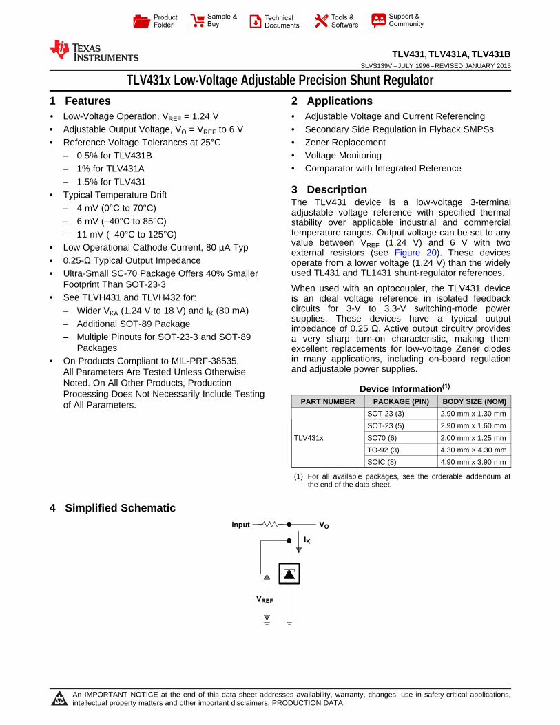
VREF
Input V
I
O
K
Product
Folder
Sample &Buy
Technical
Documents
Tools &
Software
Support &Community
TLV431, TLV431A, TLV431BSLVS139V –JULY 1996–REVISED JANUARY 2015
TLV431x Low-Voltage Adjustable Precision Shunt Regulator1 Features 2 Applications1• Low-Voltage Operation, VREF = 1.24 V • Adjustable Voltage and Current Referencing• Adjustable Output Voltage, VO = VREF to 6 V • Secondary Side Regulation in Flyback SMPSs• Reference Voltage Tolerances at 25°C • Zener Replacement
• Voltage Monitoring– 0.5% for TLV431B• Comparator with Integrated Reference– 1% for TLV431A
– 1.5% for TLV4313 Description• Typical Temperature DriftThe TLV431 device is a low-voltage 3-terminal– 4 mV (0°C to 70°C) adjustable voltage reference with specified thermal
– 6 mV (–40°C to 85°C) stability over applicable industrial and commercialtemperature ranges. Output voltage can be set to any– 11 mV (–40°C to 125°C)value between VREF (1.24 V) and 6 V with two• Low Operational Cathode Current, 80 µA Typ external resistors (see Figure 20). These devices
• 0.25-Ω Typical Output Impedance operate from a lower voltage (1.24 V) than the widelyused TL431 and TL1431 shunt-regulator references.• Ultra-Small SC-70 Package Offers 40% Smaller
Footprint Than SOT-23-3 When used with an optocoupler, the TLV431 device• See TLVH431 and TLVH432 for: is an ideal voltage reference in isolated feedback
circuits for 3-V to 3.3-V switching-mode power– Wider VKA (1.24 V to 18 V) and IK (80 mA)supplies. These devices have a typical output– Additional SOT-89 Package impedance of 0.25 Ω. Active output circuitry provides
– Multiple Pinouts for SOT-23-3 and SOT-89 a very sharp turn-on characteristic, making themPackages excellent replacements for low-voltage Zener diodes
in many applications, including on-board regulation• On Products Compliant to MIL-PRF-38535,and adjustable power supplies.All Parameters Are Tested Unless Otherwise
Noted. On All Other Products, Production Device Information(1)Processing Does Not Necessarily Include Testing
PART NUMBER PACKAGE (PIN) BODY SIZE (NOM)of All Parameters.SOT-23 (3) 2.90 mm x 1.30 mmSOT-23 (5) 2.90 mm x 1.60 mm
TLV431x SC70 (6) 2.00 mm x 1.25 mmTO-92 (3) 4.30 mm × 4.30 mmSOIC (8) 4.90 mm x 3.90 mm
(1) For all available packages, see the orderable addendum atthe end of the data sheet.
4 Simplified Schematic
1
An IMPORTANT NOTICE at the end of this data sheet addresses availability, warranty, changes, use in safety-critical applications,intellectual property matters and other important disclaimers. PRODUCTION DATA.
TLV431, TLV431A, TLV431BSLVS139V –JULY 1996–REVISED JANUARY 2015 www.ti.com
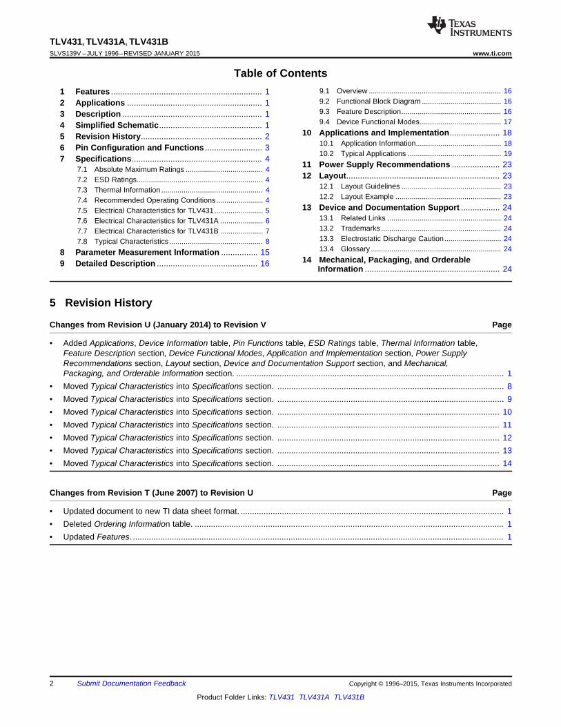
Table of Contents9.1 Overview ................................................................. 161 Features .................................................................. 19.2 Functional Block Diagram ....................................... 162 Applications ........................................................... 19.3 Feature Description................................................. 163 Description ............................................................. 19.4 Device Functional Modes........................................ 174 Simplified Schematic............................................. 1
10 Applications and Implementation...................... 185 Revision History..................................................... 210.1 Application Information.......................................... 186 Pin Configuration and Functions ......................... 310.2 Typical Applications .............................................. 197 Specifications......................................................... 4 11 Power Supply Recommendations ..................... 237.1 Absolute Maximum Ratings ...................................... 4
12 Layout................................................................... 237.2 ESD Ratings.............................................................. 412.1 Layout Guidelines ................................................. 237.3 Thermal Information .................................................. 412.2 Layout Example .................................................... 237.4 Recommended Operating Conditions....................... 4
13 Device and Documentation Support ................. 247.5 Electrical Characteristics for TLV431........................ 513.1 Related Links ........................................................ 247.6 Electrical Characteristics for TLV431A ..................... 613.2 Trademarks ........................................................... 247.7 Electrical Characteristics for TLV431B ..................... 713.3 Electrostatic Discharge Caution............................ 247.8 Typical Characteristics .............................................. 813.4 Glossary ................................................................ 248 Parameter Measurement Information ................ 15
14 Mechanical, Packaging, and Orderable9 Detailed Description ............................................ 16 Information ........................................................... 24
5 Revision History
Changes from Revision U (January 2014) to Revision V Page
• Added Applications, Device Information table, Pin Functions table, ESD Ratings table, Thermal Information table,Feature Description section, Device Functional Modes, Application and Implementation section, Power SupplyRecommendations section, Layout section, Device and Documentation Support section, and Mechanical,Packaging, and Orderable Information section. ..................................................................................................................... 1
• Moved Typical Characteristics into Specifications section. ................................................................................................... 8• Moved Typical Characteristics into Specifications section. ................................................................................................... 9• Moved Typical Characteristics into Specifications section. ................................................................................................. 10• Moved Typical Characteristics into Specifications section. ................................................................................................. 11• Moved Typical Characteristics into Specifications section. ................................................................................................. 12• Moved Typical Characteristics into Specifications section. ................................................................................................. 13• Moved Typical Characteristics into Specifications section. ................................................................................................. 14
Changes from Revision T (June 2007) to Revision U Page
• Updated document to new TI data sheet format. ................................................................................................................... 1• Deleted Ordering Information table. ....................................................................................................................................... 1• Updated Features. .................................................................................................................................................................. 1
2 Submit Documentation Feedback Copyright © 1996–2015, Texas Instruments Incorporated
Product Folder Links: TLV431 TLV431A TLV431B
REF
ANODE
CATHODE
LP (TO-92/TO-226) PACKAGE
(TOP VIEW)
DCK (SC-70) PACKAGE
(TOP VIEW)
1
2
3
6
5
4
CATHODE
NC
REF
ANODE
NC
NC
NC − No internal connection
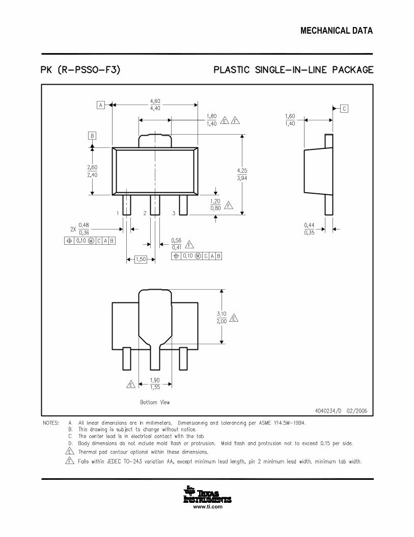
PK (SOT-89) PACKAGE
(TOP VIEW)
1
3
2
REF
CATHODE
ANODEANODE
NC − No internal connection
∗ For TLV431, TLV431A: NC − No internal connection
∗ For TLV431B: Pin 2 is attached to Substrate andmust be connected to ANODE or left open.
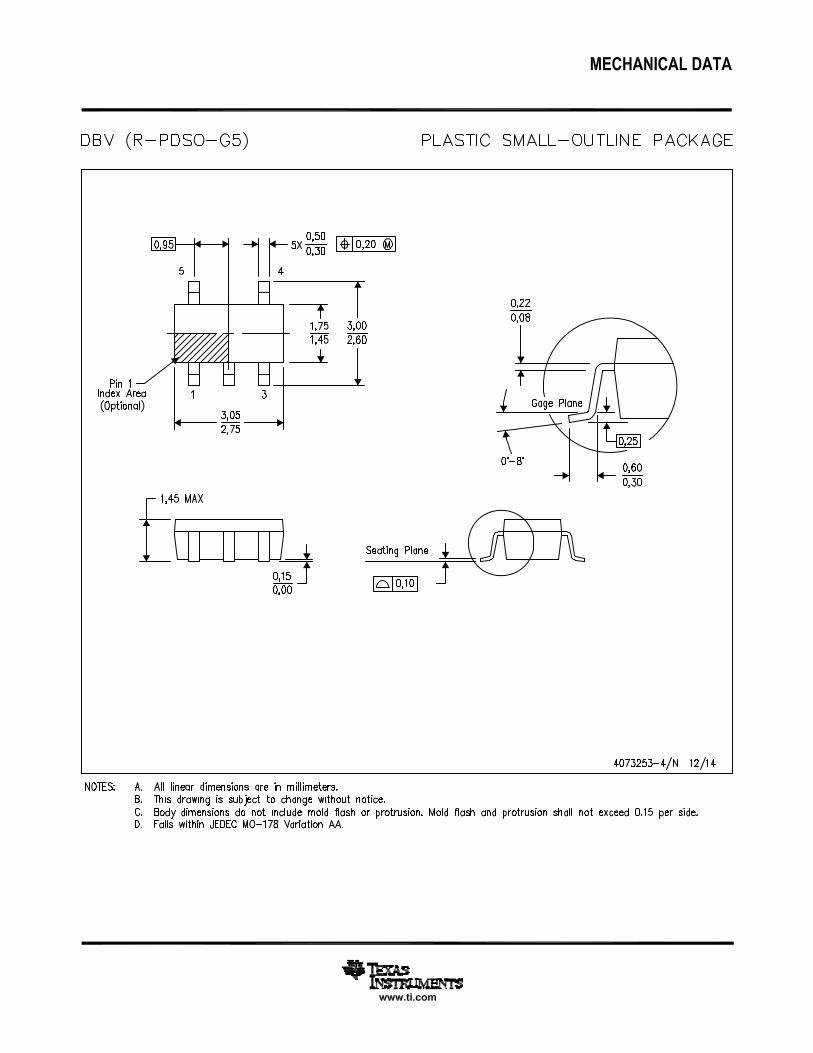
DBV (SOT-23-5) PACKAGE
(TOP VIEW)
1
2
3
5
4
NC
∗
CATHODE
ANODE
REF
DBZ (SOT-23-3) PACKAGE
(TOP VIEW)
1
2
3
REF
CATHODE
ANODE
D (SOIC) PACKAGE
(TOP VIEW)
1
2
3
4
8
7
6
5
REF
ANODE
ANODE
NC
CATHODE
ANODE
ANODE
NC
TLV431, TLV431A, TLV431Bwww.ti.com SLVS139V –JULY 1996–REVISED JANUARY 2015
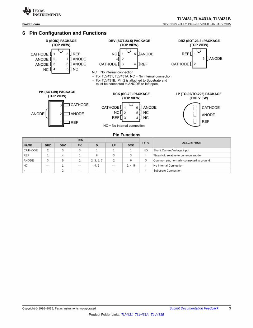
6 Pin Configuration and Functions
Pin FunctionsPIN
TYPE DESCRIPTIONNAME DBZ DBV PK D LP DCK
CATHODE 2 3 3 1 1 1 I/O Shunt Current/Voltage input
REF 1 4 1 8 3 3 I Threshold relative to common anode
ANODE 3 5 2 2, 3, 6, 7 2 6 O Common pin, normally connected to ground
NC — 1 — 4, 5 — 2, 4, 5 I No Internal Connection
* — 2 — — — — I Substrate Connection
Copyright © 1996–2015, Texas Instruments Incorporated Submit Documentation Feedback 3
Product Folder Links: TLV431 TLV431A TLV431B
TLV431, TLV431A, TLV431BSLVS139V –JULY 1996–REVISED JANUARY 2015 www.ti.com
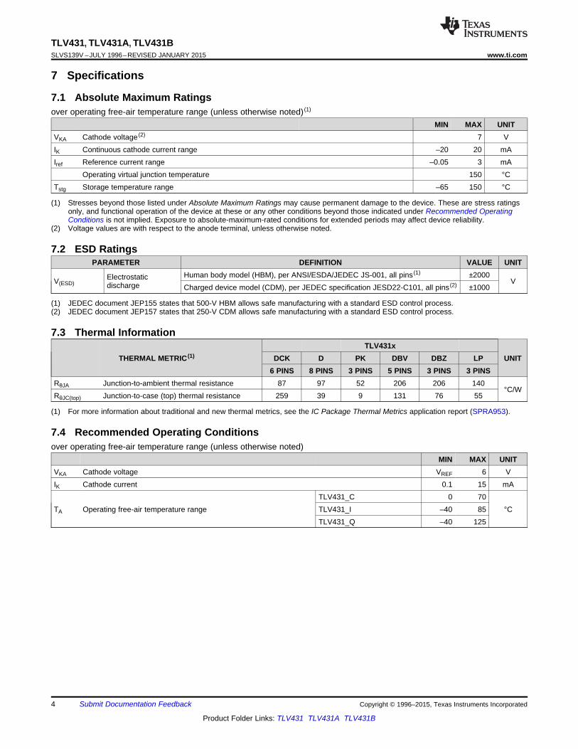
7 Specifications
7.1 Absolute Maximum Ratingsover operating free-air temperature range (unless otherwise noted) (1)
MIN MAX UNITVKA Cathode voltage (2) 7 VIK Continuous cathode current range –20 20 mAIref Reference current range –0.05 3 mA
Operating virtual junction temperature 150 °CTstg Storage temperature range –65 150 °C
(1) Stresses beyond those listed under Absolute Maximum Ratings may cause permanent damage to the device. These are stress ratingsonly, and functional operation of the device at these or any other conditions beyond those indicated under Recommended OperatingConditions is not implied. Exposure to absolute-maximum-rated conditions for extended periods may affect device reliability.
(2) Voltage values are with respect to the anode terminal, unless otherwise noted.
7.2 ESD RatingsPARAMETER DEFINITION VALUE UNIT
Human body model (HBM), per ANSI/ESDA/JEDEC JS-001, all pins (1) ±2000ElectrostaticV(ESD) Vdischarge Charged device model (CDM), per JEDEC specification JESD22-C101, all pins (2) ±1000
(1) JEDEC document JEP155 states that 500-V HBM allows safe manufacturing with a standard ESD control process.(2) JEDEC document JEP157 states that 250-V CDM allows safe manufacturing with a standard ESD control process.
7.3 Thermal InformationTLV431x
THERMAL METRIC (1) DCK D PK DBV DBZ LP UNIT6 PINS 8 PINS 3 PINS 5 PINS 3 PINS 3 PINS
RθJA Junction-to-ambient thermal resistance 87 97 52 206 206 140°C/W
RθJC(top) Junction-to-case (top) thermal resistance 259 39 9 131 76 55
(1) For more information about traditional and new thermal metrics, see the IC Package Thermal Metrics application report (SPRA953).
7.4 Recommended Operating Conditionsover operating free-air temperature range (unless otherwise noted)
MIN MAX UNITVKA Cathode voltage VREF 6 VIK Cathode current 0.1 15 mA
TLV431_C 0 70TA Operating free-air temperature range TLV431_I –40 85 °C
TLV431_Q –40 125
4 Submit Documentation Feedback Copyright © 1996–2015, Texas Instruments Incorporated
Product Folder Links: TLV431 TLV431A TLV431B
ka ka
V
z z
I
R11
R2
D
D
+¢ = » ´æ öç ÷è ø
KA
K
ka
Vz
I
D
D
=
( )REF(dev ) 6
REF A
REF
A
V10
V T 25 CppmV
C T
´= °
a =° D
æ öç ÷
æ ö è øç ÷è ø
REF
KA
V
V
D
D
(3) The dynamic impedance is defined as
TLV431, TLV431A, TLV431Bwww.ti.com SLVS139V –JULY 1996–REVISED JANUARY 2015
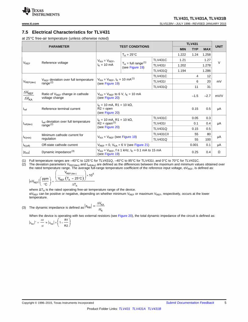
7.5 Electrical Characteristics for TLV431at 25°C free-air temperature (unless otherwise noted)
TLV431PARAMETER TEST CONDITIONS UNIT
MIN TYP MAXTA = 25°C 1.222 1.24 1.258
TLV431C 1.21 1.27VKA = VREF,VREF Reference voltage VTA = full range (1)IK = 10 mA TLV431I 1.202 1.278(see Figure 19)
TLV431Q 1.194 1.286TLV431C 4 12
VKA = VREF, IK = 10 mA (1)VREF deviation over full temperatureVREF(dev) TLV431I 6 20 mVrange (2) (see Figure 19)TLV431Q 11 31
Ratio of VREF change in cathode VKA = VREF to 6 V, IK = 10 mA –1.5 –2.7 mV/Vvoltage change (see Figure 20)
IK = 10 mA, R1 = 10 kΩ,R2 = openIref Reference terminal current 0.15 0.5 µA(see Figure 20)
TLV431C 0.05 0.3IK = 10 mA, R1 = 10 kΩ,Iref deviation over full temperatureIref(dev) R2 = open (1) TLV431I 0.1 0.4 µArange (2)(see Figure 20) TLV431Q 0.15 0.5
TLV431C/I 55 80Minimum cathode current forIK(min) VKA = VREF (see Figure 19) µAregulation TLV431Q 55 100IK(off) Off-state cathode current VREF = 0, VKA = 6 V (see Figure 21) 0.001 0.1 µA
VKA = VREF, f ≤ 1 kHz, IK = 0.1 mA to 15 mA|zKA| Dynamic impedance (3) 0.25 0.4 Ω(see Figure 19)
(1) Full temperature ranges are –40°C to 125°C for TLV431Q, –40°C to 85°C for TLV431I, and 0°C to 70°C for TLV431C.(2) The deviation parameters VREF(dev) and Iref(dev) are defined as the differences between the maximum and minimum values obtained over
the rated temperature range. The average full-range temperature coefficient of the reference input voltage, αVREF, is defined as:
where ΔTA is the rated operating free-air temperature range of the device.αVREF can be positive or negative, depending on whether minimum VREF or maximum VREF, respectively, occurs at the lowertemperature.
spacerWhen the device is operating with two external resistors (see Figure 20), the total dynamic impedance of the circuit is defined as:
Copyright © 1996–2015, Texas Instruments Incorporated Submit Documentation Feedback 5
Product Folder Links: TLV431 TLV431A TLV431B
ka ka
V
z z
I
R11
R2
D
D
+¢ = » ´æ öç ÷è ø
KA
K
ka
Vz
I
D
D
=
( )REF(dev ) 6
REF A
REF
A
V10
V T 25 CppmV
C T
´= °
a =° D
æ öç ÷
æ ö è øç ÷è ø
REF
KA
V
V
D
D
(3) The dynamic impedance is defined as
TLV431, TLV431A, TLV431BSLVS139V –JULY 1996–REVISED JANUARY 2015 www.ti.com
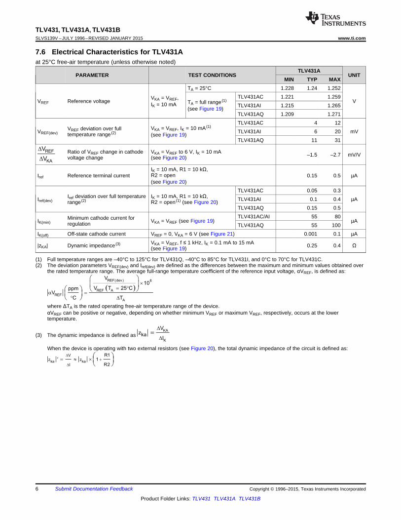
7.6 Electrical Characteristics for TLV431Aat 25°C free-air temperature (unless otherwise noted)
TLV431APARAMETER TEST CONDITIONS UNIT
MIN TYP MAXTA = 25°C 1.228 1.24 1.252
TLV431AC 1.221 1.259VKA = VREF,VREF Reference voltage VTA = full range (1)IK = 10 mA TLV431AI 1.215 1.265(see Figure 19)
TLV431AQ 1.209 1.271TLV431AC 4 12
VKA = VREF, IK = 10 mA (1)VREF deviation over fullVREF(dev) TLV431AI 6 20 mVtemperature range (2) (see Figure 19)TLV431AQ 11 31
Ratio of VREF change in cathode VKA = VREF to 6 V, IK = 10 mA –1.5 –2.7 mV/Vvoltage change (see Figure 20)
IK = 10 mA, R1 = 10 kΩ,R2 = openIref Reference terminal current 0.15 0.5 µA(see Figure 20)
TLV431AC 0.05 0.3Iref deviation over full temperature IK = 10 mA, R1 = 10 kΩ,Iref(dev) TLV431AI 0.1 0.4 µArange (2) R2 = open (1) (see Figure 20)
TLV431AQ 0.15 0.5TLV431AC/AI 55 80Minimum cathode current forIK(min) VKA = VREF (see Figure 19) µAregulation TLV431AQ 55 100
IK(off) Off-state cathode current VREF = 0, VKA = 6 V (see Figure 21) 0.001 0.1 µAVKA = VREF, f ≤ 1 kHz, IK = 0.1 mA to 15 mA|zKA| Dynamic impedance (3) 0.25 0.4 Ω(see Figure 19)
(1) Full temperature ranges are –40°C to 125°C for TLV431Q, –40°C to 85°C for TLV431I, and 0°C to 70°C for TLV431C.(2) The deviation parameters VREF(dev) and Iref(dev) are defined as the differences between the maximum and minimum values obtained over
the rated temperature range. The average full-range temperature coefficient of the reference input voltage, αVREF, is defined as:
where ΔTA is the rated operating free-air temperature range of the device.αVREF can be positive or negative, depending on whether minimum VREF or maximum VREF, respectively, occurs at the lowertemperature.
spacerWhen the device is operating with two external resistors (see Figure 20), the total dynamic impedance of the circuit is defined as:
6 Submit Documentation Feedback Copyright © 1996–2015, Texas Instruments Incorporated
Product Folder Links: TLV431 TLV431A TLV431B
ka ka
V
z z
I
R11
R2
D
D
+¢ = » ´æ öç ÷è ø
KA
K
ka
Vz
I
D
D
=
( )REF(dev ) 6
REF A
REF
A
V10
V T 25 CppmV
C T
´= °
a =° D
æ öç ÷
æ ö è øç ÷è ø
REF
KA
V
V
D
D
(4) The dynamic impedance is defined as
TLV431, TLV431A, TLV431Bwww.ti.com SLVS139V –JULY 1996–REVISED JANUARY 2015
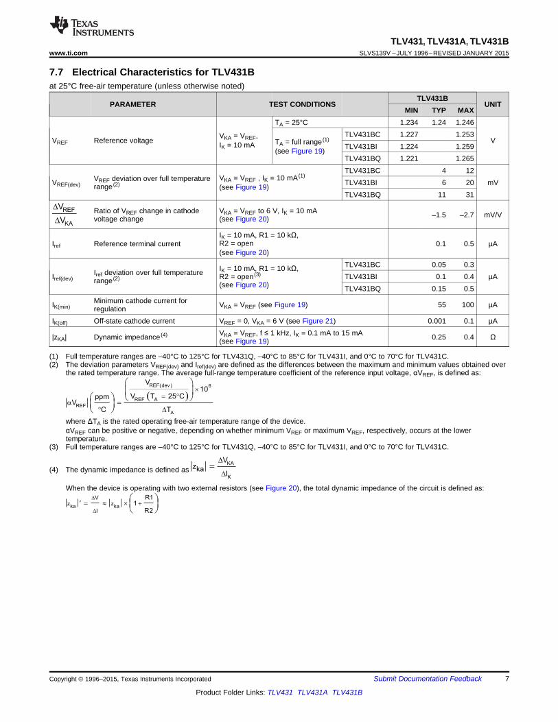
7.7 Electrical Characteristics for TLV431Bat 25°C free-air temperature (unless otherwise noted)
TLV431BPARAMETER TEST CONDITIONS UNIT
MIN TYP MAXTA = 25°C 1.234 1.24 1.246
TLV431BC 1.227 1.253VKA = VREF,VREF Reference voltage VTA = full range (1)IK = 10 mA TLV431BI 1.224 1.259(see Figure 19)
TLV431BQ 1.221 1.265TLV431BC 4 12
VKA = VREF , IK = 10 mA (1)VREF deviation over full temperatureVREF(dev) TLV431BI 6 20 mVrange (2) (see Figure 19)TLV431BQ 11 31
Ratio of VREF change in cathode VKA = VREF to 6 V, IK = 10 mA –1.5 –2.7 mV/Vvoltage change (see Figure 20)
IK = 10 mA, R1 = 10 kΩ,R2 = openIref Reference terminal current 0.1 0.5 µA(see Figure 20)
TLV431BC 0.05 0.3IK = 10 mA, R1 = 10 kΩ,Iref deviation over full temperatureIref(dev) R2 = open (3) TLV431BI 0.1 0.4 µArange (2)(see Figure 20) TLV431BQ 0.15 0.5
Minimum cathode current forIK(min) VKA = VREF (see Figure 19) 55 100 µAregulationIK(off) Off-state cathode current VREF = 0, VKA = 6 V (see Figure 21) 0.001 0.1 µA
VKA = VREF, f ≤ 1 kHz, IK = 0.1 mA to 15 mA|zKA| Dynamic impedance (4) 0.25 0.4 Ω(see Figure 19)
(1) Full temperature ranges are –40°C to 125°C for TLV431Q, –40°C to 85°C for TLV431I, and 0°C to 70°C for TLV431C.(2) The deviation parameters VREF(dev) and Iref(dev) are defined as the differences between the maximum and minimum values obtained over
the rated temperature range. The average full-range temperature coefficient of the reference input voltage, αVREF, is defined as:
where ΔTA is the rated operating free-air temperature range of the device.αVREF can be positive or negative, depending on whether minimum VREF or maximum VREF, respectively, occurs at the lowertemperature.
(3) Full temperature ranges are –40°C to 125°C for TLV431Q, –40°C to 85°C for TLV431I, and 0°C to 70°C for TLV431C.
spacerWhen the device is operating with two external resistors (see Figure 20), the total dynamic impedance of the circuit is defined as:
Copyright © 1996–2015, Texas Instruments Incorporated Submit Documentation Feedback 7
Product Folder Links: TLV431 TLV431A TLV431B
−C
ath
od
e C
urr
en
t−
250
200
150
100
50
0
−200
−250
−1 −0.5 0 0.5 1 1.5
I KA
µ
VKA − Cathode Voltage − V
−50
−100
−150
VKA = VREF
TA = 25°C
Temperature (qC)
Ik(m
in)
-40 -20 0 20 40 60 80 100 120 14055
60
65
70
75
80
85
90
95
100
105
110
115
120
50
70
90
110
130
150
170
190
210
230
250
−50 −25 0 25 50 75 100 125 150
IK = 10 mA
R1 = 10 kΩ
R2 = Open
−R
efe
ren
ce
Inp
ut
Cu
rren
t−
nA
I ref
TJ − Junction Temperature − °C
−C
ath
od
e C
urr
en
t−
mA
15
10
5
0
−5
−10
−15−1 −0.5 0 0.5 1 1.5
I K
VKA = VREF
TA = 25°C
VKA − Cathode Voltage − V
1.246
1.242
1.240
1.238
−R
efe
ren
ce
Vo
ltag
e−
V 1.250
1.252
1.254
1.248
1.244
−50 −25 0 25 50 75 100 125 150
IK = 10 mA
Vre
f
TJ − Junction Temperature − °C
150
100
50
−R
efe
ren
ce
Inp
ut
Cu
rren
t−
nA
200
250
−50 −25 0 25 50 75 100 125 150
I re
f
TJ − Junction Temperature − °C
IK = 10 mA
R1 = 10 kΩ
R2 = Open
TLV431, TLV431A, TLV431BSLVS139V –JULY 1996–REVISED JANUARY 2015 www.ti.com
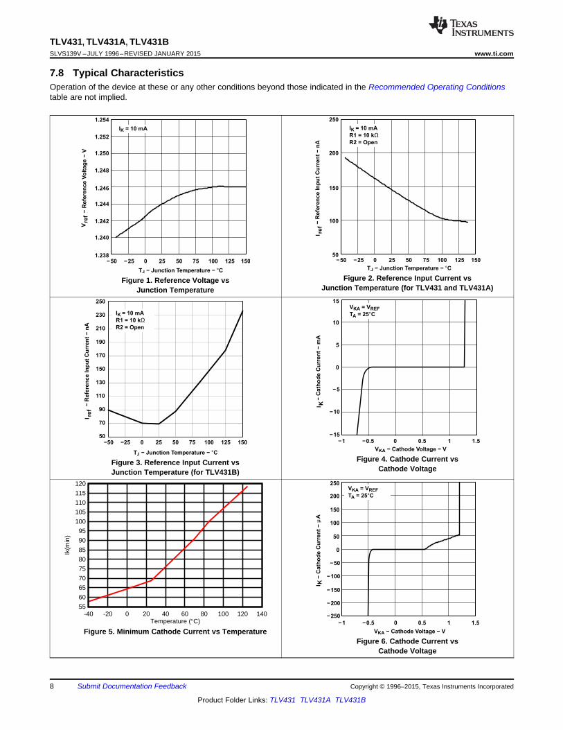
7.8 Typical CharacteristicsOperation of the device at these or any other conditions beyond those indicated in the Recommended Operating Conditionstable are not implied.
Figure 2. Reference Input Current vsFigure 1. Reference Voltage vsJunction Temperature (for TLV431 and TLV431A)Junction Temperature
Figure 4. Cathode Current vsFigure 3. Reference Input Current vsCathode VoltageJunction Temperature (for TLV431B)
Figure 5. Minimum Cathode Current vs TemperatureFigure 6. Cathode Current vs
Cathode Voltage
8 Submit Documentation Feedback Copyright © 1996–2015, Texas Instruments Incorporated
Product Folder Links: TLV431 TLV431A TLV431B
−1.0
−0.9
−0.8
−0.7
−0.6
−0.5
−0.4
−0.3
−0.2
−0.1
0.0
−50 −25 0 25 50 75 100 125 150
IK = 10 mA
∆VKA = VREF to 6 V
−1
0
TJ − Junction Temperature − °C
−R
ati
oo
fD
elt
aR
efe
ren
ce
Vo
ltag
e
toD
elt
aC
ath
od
eV
olt
ag
e−
mV
/V
Vre
f/∆
VK
A∆
−R
ati
oo
fD
elt
aR
efe
ren
ce
Vo
ltag
e
0
−0.1
−0.2
−0.3
−0.4
−0.5
−0.6
−0.7
−0.8
toD
elt
aC
ath
od
eV
olt
ag
e−
mV
/V
Vre
f/∆
VK
A∆
−50 −25 0 25 50 75 100 125 150
TJ − Junction Temperature − °C
IK = 10 mA
∆VKA = VREF to 6 V
20
10
0
−O
ff-S
tate
Cath
od
e C
urr
en
t−
nA
30
40
−50 −25 0 25 50 75 100 125
I K(o
ff)
TJ − Junction Temperature − °C
VKA = 5 V
VREF = 0
150
0
500
1000
1500
2000
2500
3000
−50 −25 0 25 50 75 100 125 150
VKA = 6 V
VREF = 0
TJ − Junction Temperature − °C
−O
ff-S
tate
Cath
od
e C
urr
en
t−
nA
I K(o
ff)
TLV431, TLV431A, TLV431Bwww.ti.com SLVS139V –JULY 1996–REVISED JANUARY 2015
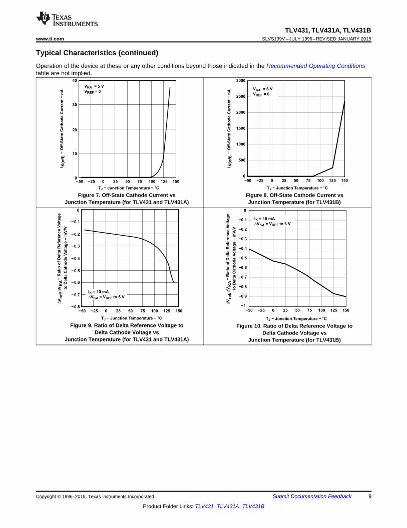
Typical Characteristics (continued)Operation of the device at these or any other conditions beyond those indicated in the Recommended Operating Conditionstable are not implied.
Figure 7. Off-State Cathode Current vs Figure 8. Off-State Cathode Current vsJunction Temperature (for TLV431 and TLV431A) Junction Temperature (for TLV431B)
Figure 9. Ratio of Delta Reference Voltage to Figure 10. Ratio of Delta Reference Voltage toDelta Cathode Voltage vs Delta Cathode Voltage vs
Junction Temperature (for TLV431 and TLV431A) Junction Temperature (for TLV431B)
Copyright © 1996–2015, Texas Instruments Incorporated Submit Documentation Feedback 9
Product Folder Links: TLV431 TLV431A TLV431B
200
15010 100 1k
−E
qu
ivale
nt
Inp
ut
No
ise
Vo
ltag
e−
f − Frequency − Hz
10k 100k
300
250
Vn
nV
/H
z
VKA = VREF
IK = 1 mA
TA = 25°C
_
+
820 Ω
+2200 µF
750 Ω
1 kΩ
470 µF
3 V
TLV431
or
TLV431A
or
TLV431B
TP
160 kΩ
160 Ω
TLE2027
TEST CIRCUIT FOR EQUIVALENT INPUT NOISE VOLTAGE
+
−0.025
−0.075
−0.1
−0.125
Perc
en
tag
eC
han
ge
inV
ref
−%
0.025
−0.05
0 10 20 30 40 50 60
IK = 1 mA
Vre
f
Operating Life at 55°C − kh‡
% Change (3δ
% Change (−3δ)
% Change (avg)
)
TLV431, TLV431A, TLV431BSLVS139V –JULY 1996–REVISED JANUARY 2015 www.ti.com
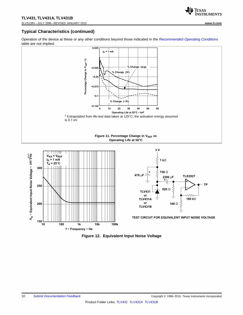
Typical Characteristics (continued)Operation of the device at these or any other conditions beyond those indicated in the Recommended Operating Conditionstable are not implied.
‡ Extrapolated from life-test data taken at 125°C; the activation energy assumedis 0.7 eV.
Figure 11. Percentage Change in VREF vsOperating Life at 55°C
Figure 12. Equivalent Input Noise Voltage
10 Submit Documentation Feedback Copyright © 1996–2015, Texas Instruments Incorporated
Product Folder Links: TLV431 TLV431A TLV431B
0 2 4 6
t − Time − s
EQUIVALENT INPUT NOISE VOLTAGE
OVER A 10-s PERIOD
8 10
10
8
6
4
2
0
−2
−4
−6
−8
−10
f = 0.1 Hz to 10 Hz
IK = 1 mA
TA = 25°C
−E
qu
ivale
nt
Inp
ut
No
ise
Vo
ltag
e−
Vn
Vµ
_
+
1 µF
750 Ω
1 kΩ
470 µF
3 V
TLV431
or
TLV431A
or
TLV431B
33 kΩ
TLE2027
TEST CIRCUIT FOR 0.1-Hz TO 10-Hz EQUIVALENT NOISE VOLTAGE
+
33 kΩ
10 kΩ
_
+
16 Ω0.1 µF
160 kΩ820 Ω
+
2200 µFTP
2.2 µF
CRO 1 MΩ
TLE2027
0.47 µF
10 kΩ
+
TLV431, TLV431A, TLV431Bwww.ti.com SLVS139V –JULY 1996–REVISED JANUARY 2015
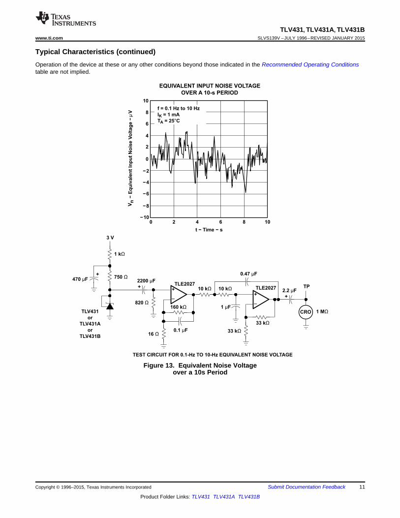
Typical Characteristics (continued)Operation of the device at these or any other conditions beyond those indicated in the Recommended Operating Conditionstable are not implied.
Figure 13. Equivalent Noise Voltageover a 10s Period
Copyright © 1996–2015, Texas Instruments Incorporated Submit Documentation Feedback 11
Product Folder Links: TLV431 TLV431A TLV431B
100 Ω
100 Ω
GND
Output
IK
0.1
1k 10k 100k 1M 10M
−R
efe
ren
ce Im
ped
an
ce
−
1
f − Frequency − Hz
REFERENCE IMPEDANCE
vs
FREQUENCY
10
100
ka
|z|
Ω
IK = 0.1 mA to 15 mA
TA = 25°C
TEST CIRCUIT FOR REFERENCE IMPEDANCE
0.01
−
+
SMALL-SIGNAL VOLTAGE GAIN/PHASE MARGIN
vs
FREQUENCY
10
Fµ
GND
Output
180 Ω
IK6.8 kΩ
1k 10k 100k 1M100
−S
mall-S
ign
alV
olt
ag
eG
ain
/Ph
ase
Marg
in−
dB
f − Frequency − Hz
AV
TEST CIRCUIT FOR VOLTAGE GAIN
AND PHASE MARGIN
80
70
60
50
40
30
20
10
0
−10
0°
36°
72°
108°
144°
180°
Ph
ase S
hif
t
4.3 kΩ
5 V
IK = 10 mA
TA = 25°C
−20
TLV431, TLV431A, TLV431BSLVS139V –JULY 1996–REVISED JANUARY 2015 www.ti.com
Typical Characteristics (continued)Operation of the device at these or any other conditions beyond those indicated in the Recommended Operating Conditionstable are not implied.
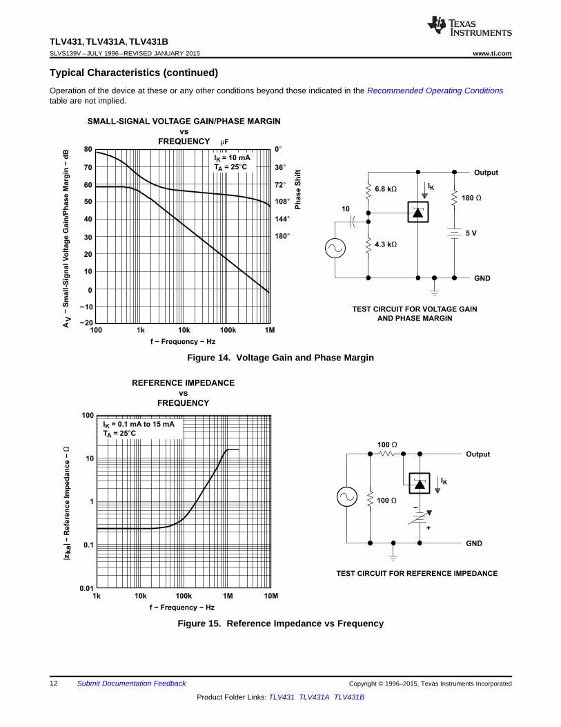
Figure 14. Voltage Gain and Phase Margin
Figure 15. Reference Impedance vs Frequency
12 Submit Documentation Feedback Copyright © 1996–2015, Texas Instruments Incorporated
Product Folder Links: TLV431 TLV431A TLV431B
Inp
ut
an
dO
utp
ut
Vo
ltag
e−
V
Output
R = 1.8 kΩ
TA = 25°C
1.8 kΩ
50 Ω
GND
Output
Pulse
Generator
f = 100 kHz
TEST CIRCUIT FOR PULSE RESPONSE 2
0 1 2 3 4
PULSE RESPONSE 2
5 6 7 8
3.5
3
2.5
2
1.5
1
0.5
0
−0.5
t − Time − µs
Input
IK
Inp
ut
an
dO
utp
ut
Vo
ltag
e−
V
Output
R = 18 kΩ
TA = 25°C
18 kΩ
50 Ω
GND
Output
Pulse
Generator
f = 100 kHz
TEST CIRCUIT FOR PULSE RESPONSE 1
0 1 2 3 4
PULSE RESPONSE 1
5 6 7 8
3.5
3
2.5
2
1.5
1
0.5
0
−0.5
t − Time − µs
Input
Ik
TLV431, TLV431A, TLV431Bwww.ti.com SLVS139V –JULY 1996–REVISED JANUARY 2015
Typical Characteristics (continued)Operation of the device at these or any other conditions beyond those indicated in the Recommended Operating Conditionstable are not implied.
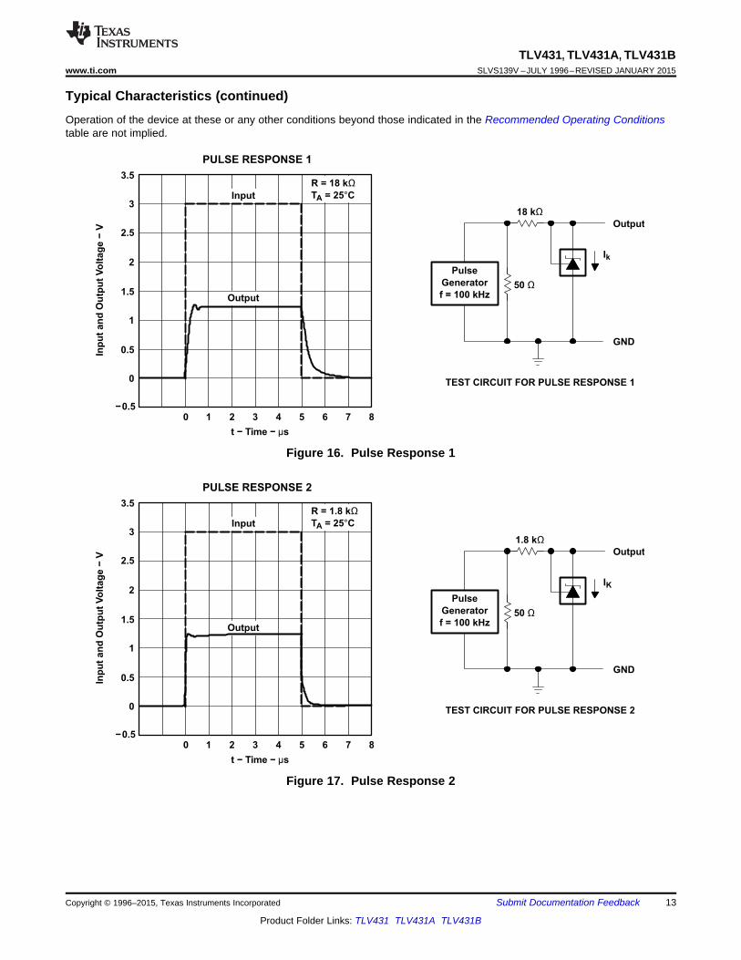
Figure 16. Pulse Response 1
Figure 17. Pulse Response 2
Copyright © 1996–2015, Texas Instruments Incorporated Submit Documentation Feedback 13
Product Folder Links: TLV431 TLV431A TLV431B
9
6
0
15
0.001 0.01 0.1 1 10
−C
ath
od
e C
urr
en
t−
mA
12
STABILITY BOUNDARY CONDITION‡
(for TLV431 and TLV431A)
3
I K
CL − Load Capacitance − µF
Stable
VKA = VREF
VKA = 2 V
Stable
VKA = 3 V
TA = 25°C
150 Ω
CL Vbat
IK
TEST CIRCUIT FOR VKA = VREF
150 Ω
CL Vbat
IKR1 = 10 kΩ
R2
TEST CIRCUIT FOR VKA = 2 V, 3 V
−
+
−
+
IK = 15 mA Max
−C
ath
od
e C
urr
en
t−
mA
STABILITY BOUNDARY CONDITION‡
(for TLV431B)
I K
CL − Load Capacitance − µF
9
6
0
15
0.001 0.01 0.1 1 10
12
3
Stable
VKA = 3 V
Stable
Unstable
VKA = 2 V
TA = 25°C
IK = 15 mA MAX
For VKA = VREF ,
Stable for CL = 1 pF to 10k nF
TLV431, TLV431A, TLV431BSLVS139V –JULY 1996–REVISED JANUARY 2015 www.ti.com
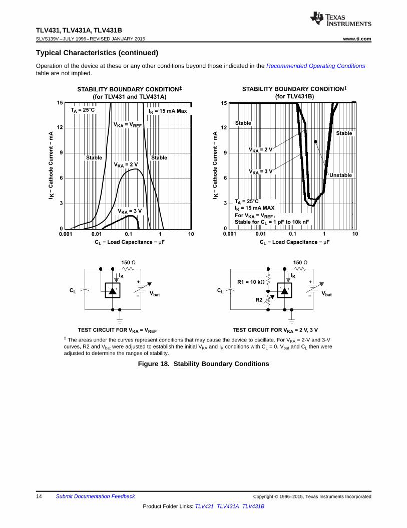
Typical Characteristics (continued)Operation of the device at these or any other conditions beyond those indicated in the Recommended Operating Conditionstable are not implied.
‡ The areas under the curves represent conditions that may cause the device to oscillate. For VKA = 2-V and 3-Vcurves, R2 and Vbat were adjusted to establish the initial VKA and IK conditions with CL = 0. Vbat and CL then wereadjusted to determine the ranges of stability.
Figure 18. Stability Boundary Conditions
14 Submit Documentation Feedback Copyright © 1996–2015, Texas Instruments Incorporated
Product Folder Links: TLV431 TLV431A TLV431B
IK(off)
VOInput
Iref
IK
VOInput
VREF
R1
R2
VREF
Input V
I
O
K
TLV431, TLV431A, TLV431Bwww.ti.com SLVS139V –JULY 1996–REVISED JANUARY 2015
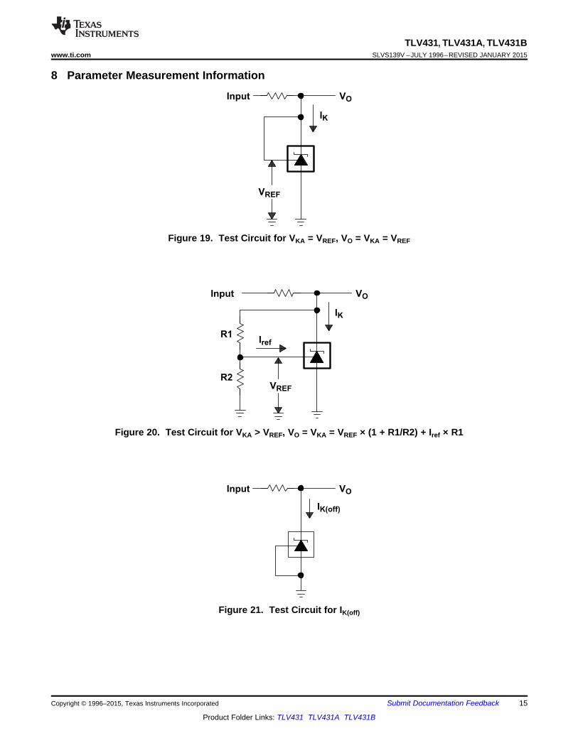
8 Parameter Measurement Information
Figure 19. Test Circuit for VKA = VREF, VO = VKA = VREFxxxxxxxxx
Figure 20. Test Circuit for VKA > VREF, VO = VKA = VREF × (1 + R1/R2) + Iref × R1xxxxxxxxx
Figure 21. Test Circuit for IK(off)
Copyright © 1996–2015, Texas Instruments Incorporated Submit Documentation Feedback 15
Product Folder Links: TLV431 TLV431A TLV431B
CATHODE
REF
ANODE
+
_
Vref
TLV431, TLV431A, TLV431BSLVS139V –JULY 1996–REVISED JANUARY 2015 www.ti.com
9 Detailed Description
9.1 OverviewTLV431 is a low power counterpart to TL431, having lower reference voltage (1.24 V vs 2.5 V) for lower voltageadjustability and lower minimum cathode current (Ik(min)=100 µA vs 1 mA). Like TL431, TLV431 is used inconjunction with it's key components to behave as a single voltage reference, error amplifier, voltage clamp orcomparator with integrated reference.
TLV431 can be operated and adjusted to cathode voltages from 1.24V to 6V, making this part optimum for awide range of end equipments in industrial, auto, telecom & computing. In order for this device to behave as ashunt regulator or error amplifier, > 100 µA (Imin(max)) must be supplied in to the cathode pin. Under thiscondition, feedback can be applied from the Cathode and Ref pins to create a replica of the internal referencevoltage.
Various reference voltage options can be purchased with initial tolerances (at 25°C) of 0.5%, 1%, and 1.5%.These reference options are denoted by B (0.5%), A (1.0%) and blank (1.5%) after the TLV431.
The TLV431xC devices are characterized for operation from 0°C to 70°C, the TLV431xI devices arecharacterized for operation from –40°C to 85°C, and the TLV431xQ devices are characterized for operation from–40°C to 125°C.
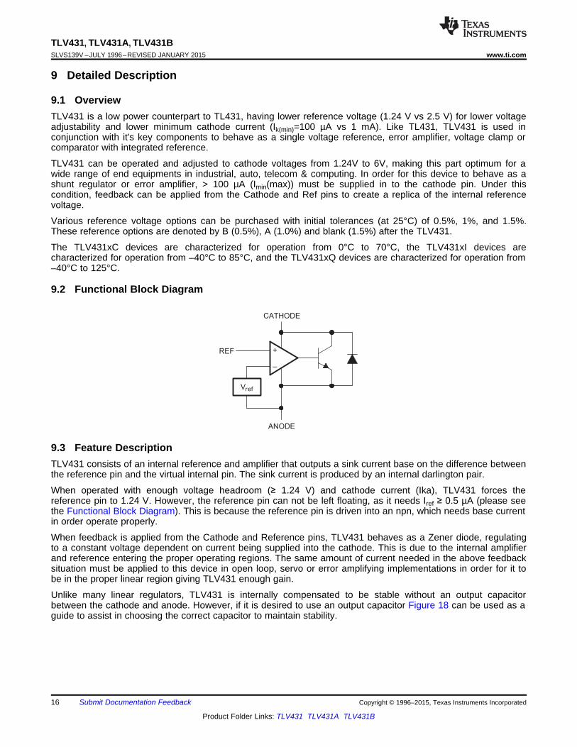
9.2 Functional Block Diagram
9.3 Feature DescriptionTLV431 consists of an internal reference and amplifier that outputs a sink current base on the difference betweenthe reference pin and the virtual internal pin. The sink current is produced by an internal darlington pair.
When operated with enough voltage headroom (≥ 1.24 V) and cathode current (Ika), TLV431 forces thereference pin to 1.24 V. However, the reference pin can not be left floating, as it needs Iref ≥ 0.5 µA (please seethe Functional Block Diagram). This is because the reference pin is driven into an npn, which needs base currentin order operate properly.
When feedback is applied from the Cathode and Reference pins, TLV431 behaves as a Zener diode, regulatingto a constant voltage dependent on current being supplied into the cathode. This is due to the internal amplifierand reference entering the proper operating regions. The same amount of current needed in the above feedbacksituation must be applied to this device in open loop, servo or error amplifying implementations in order for it tobe in the proper linear region giving TLV431 enough gain.
Unlike many linear regulators, TLV431 is internally compensated to be stable without an output capacitorbetween the cathode and anode. However, if it is desired to use an output capacitor Figure 18 can be used as aguide to assist in choosing the correct capacitor to maintain stability.
16 Submit Documentation Feedback Copyright © 1996–2015, Texas Instruments Incorporated
Product Folder Links: TLV431 TLV431A TLV431B
TLV431, TLV431A, TLV431Bwww.ti.com SLVS139V –JULY 1996–REVISED JANUARY 2015
9.4 Device Functional Modes
9.4.1 Open Loop (Comparator)When the cathode/output voltage or current of TLV431 is not being fed back to the reference/input pin in anyform, this device is operating in open loop. With proper cathode current (Ika) applied to this device, TLV431 willhave the characteristics shown in Figure 6. With such high gain in this configuration, TLV431 is typically used asa comparator. With the reference integrated makes TLV431 the preferred choice when users are trying tomonitor a certain level of a single signal.
9.4.2 Closed LoopWhen the cathode/output voltage or current of TLV431 is being fed back to the reference/input pin in any form,this device is operating in closed loop. The majority of applications involving TLV431 use it in this manner toregulate a fixed voltage or current. The feedback enables this device to behave as an error amplifier, computinga portion of the output voltage and adjusting it to maintain the desired regulation. This is done by relating theoutput voltage back to the reference pin in a manner to make it equal to the internal reference voltage, which canbe accomplished via resistive or direct feedback.
Copyright © 1996–2015, Texas Instruments Incorporated Submit Documentation Feedback 17
Product Folder Links: TLV431 TLV431A TLV431B
~
~
P
− +
P
P
VCC
VFB
Current
Sense
Gate Drive
GND
Controller
P
P P P
TLV431
or
TLV431A
or
TLV431B
VO
3.3 V
VI
120 V
TLV431, TLV431A, TLV431BSLVS139V –JULY 1996–REVISED JANUARY 2015 www.ti.com
10 Applications and Implementation
NOTEInformation in the following applications sections is not part of the TI componentspecification, and TI does not warrant its accuracy or completeness. TI’s customers areresponsible for determining suitability of components for their purposes. Customers shouldvalidate and test their design implementation to confirm system functionality.
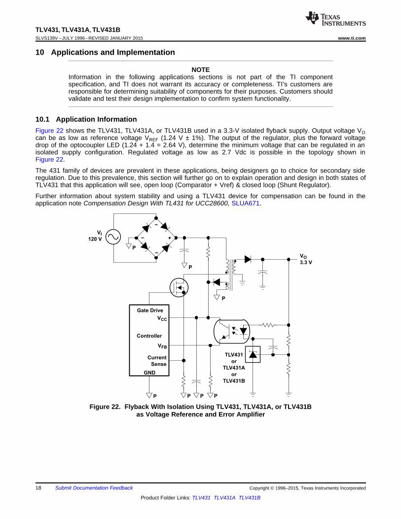
10.1 Application InformationFigure 22 shows the TLV431, TLV431A, or TLV431B used in a 3.3-V isolated flyback supply. Output voltage VOcan be as low as reference voltage VREF (1.24 V ± 1%). The output of the regulator, plus the forward voltagedrop of the optocoupler LED (1.24 + 1.4 = 2.64 V), determine the minimum voltage that can be regulated in anisolated supply configuration. Regulated voltage as low as 2.7 Vdc is possible in the topology shown inFigure 22.
The 431 family of devices are prevalent in these applications, being designers go to choice for secondary sideregulation. Due to this prevalence, this section will further go on to explain operation and design in both states ofTLV431 that this application will see, open loop (Comparator + Vref) & closed loop (Shunt Regulator).
Further information about system stability and using a TLV431 device for compensation can be found in theapplication note Compensation Design With TL431 for UCC28600, SLUA671.
Figure 22. Flyback With Isolation Using TLV431, TLV431A, or TLV431Bas Voltage Reference and Error Amplifier
18 Submit Documentation Feedback Copyright © 1996–2015, Texas Instruments Incorporated
Product Folder Links: TLV431 TLV431A TLV431B
+
1.24 V
CATHODE
ANODE
REFVIN
Vout
Vsup
Rsup
R1
R2
VL
RIN
TLV431, TLV431A, TLV431Bwww.ti.com SLVS139V –JULY 1996–REVISED JANUARY 2015
10.2 Typical Applications
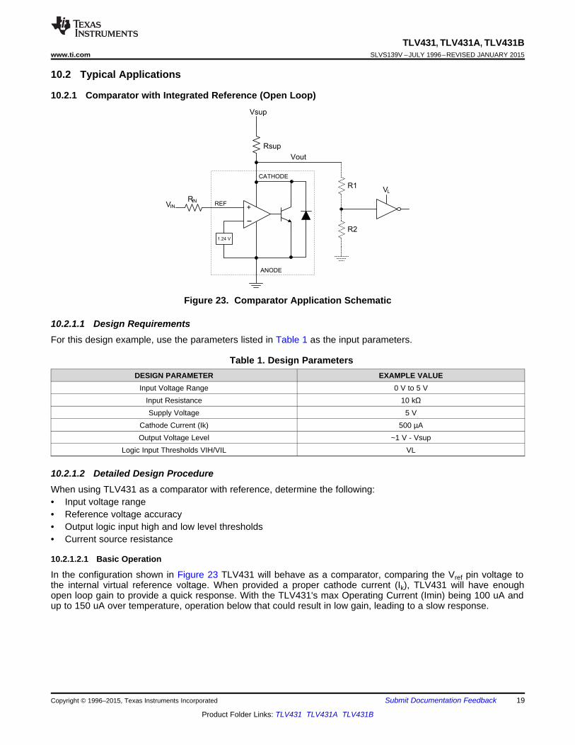
10.2.1 Comparator with Integrated Reference (Open Loop)
Figure 23. Comparator Application Schematic
10.2.1.1 Design RequirementsFor this design example, use the parameters listed in Table 1 as the input parameters.
Table 1. Design ParametersDESIGN PARAMETER EXAMPLE VALUE
Input Voltage Range 0 V to 5 VInput Resistance 10 kΩSupply Voltage 5 V
Cathode Current (Ik) 500 µAOutput Voltage Level ~1 V - Vsup
Logic Input Thresholds VIH/VIL VL
10.2.1.2 Detailed Design ProcedureWhen using TLV431 as a comparator with reference, determine the following:• Input voltage range• Reference voltage accuracy• Output logic input high and low level thresholds• Current source resistance
10.2.1.2.1 Basic Operation
In the configuration shown in Figure 23 TLV431 will behave as a comparator, comparing the Vref pin voltage tothe internal virtual reference voltage. When provided a proper cathode current (Ik), TLV431 will have enoughopen loop gain to provide a quick response. With the TLV431's max Operating Current (Imin) being 100 uA andup to 150 uA over temperature, operation below that could result in low gain, leading to a slow response.
Copyright © 1996–2015, Texas Instruments Incorporated Submit Documentation Feedback 19
Product Folder Links: TLV431 TLV431A TLV431B
Time (ms)
Vol
tage
(V
)
-0.4 -0.2 0 0.2 0.4 0.6 0.8-2-10123456789
101112
D001
Vin~1.24V (+/-5%)Vo(Vin=1.18V)Vo(Vin=1.24V)Vo(Vin=1.30V)
Time (ms)
Vol
tage
(V
)
-0.4 -0.2 0 0.2 0.4 0.6 0.8-2
-1
0
1
2
3
4
5
6
7
8
9
10
D001
Vo(Vin=5.0V)Vin=5.0V
TLV431, TLV431A, TLV431BSLVS139V –JULY 1996–REVISED JANUARY 2015 www.ti.com
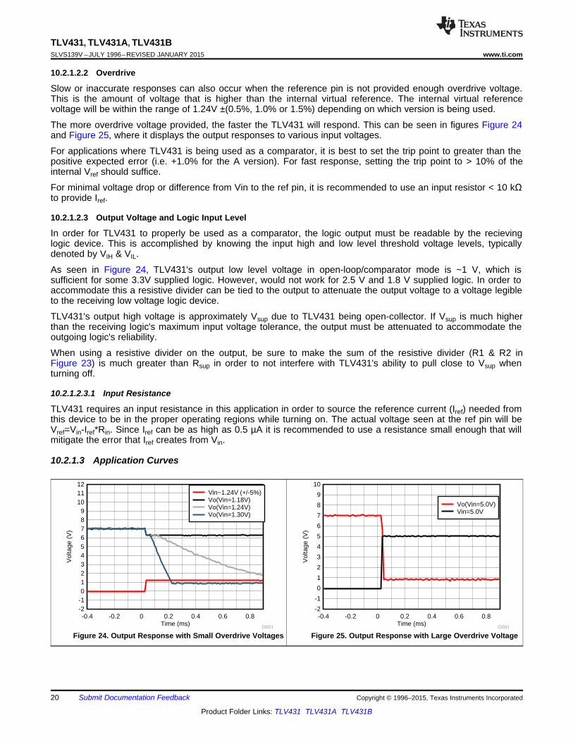
10.2.1.2.2 Overdrive
Slow or inaccurate responses can also occur when the reference pin is not provided enough overdrive voltage.This is the amount of voltage that is higher than the internal virtual reference. The internal virtual referencevoltage will be within the range of 1.24V ±(0.5%, 1.0% or 1.5%) depending on which version is being used.
The more overdrive voltage provided, the faster the TLV431 will respond. This can be seen in figures Figure 24and Figure 25, where it displays the output responses to various input voltages.
For applications where TLV431 is being used as a comparator, it is best to set the trip point to greater than thepositive expected error (i.e. +1.0% for the A version). For fast response, setting the trip point to > 10% of theinternal Vref should suffice.
For minimal voltage drop or difference from Vin to the ref pin, it is recommended to use an input resistor < 10 kΩto provide Iref.
10.2.1.2.3 Output Voltage and Logic Input Level
In order for TLV431 to properly be used as a comparator, the logic output must be readable by the recievinglogic device. This is accomplished by knowing the input high and low level threshold voltage levels, typicallydenoted by VIH & VIL.
As seen in Figure 24, TLV431's output low level voltage in open-loop/comparator mode is ~1 V, which issufficient for some 3.3V supplied logic. However, would not work for 2.5 V and 1.8 V supplied logic. In order toaccommodate this a resistive divider can be tied to the output to attenuate the output voltage to a voltage legibleto the receiving low voltage logic device.
TLV431's output high voltage is approximately Vsup due to TLV431 being open-collector. If Vsup is much higherthan the receiving logic's maximum input voltage tolerance, the output must be attenuated to accommodate theoutgoing logic's reliability.
When using a resistive divider on the output, be sure to make the sum of the resistive divider (R1 & R2 inFigure 23) is much greater than Rsup in order to not interfere with TLV431's ability to pull close to Vsup whenturning off.
10.2.1.2.3.1 Input Resistance
TLV431 requires an input resistance in this application in order to source the reference current (Iref) needed fromthis device to be in the proper operating regions while turning on. The actual voltage seen at the ref pin will beVref=Vin-Iref*Rin. Since Iref can be as high as 0.5 µA it is recommended to use a resistance small enough that willmitigate the error that Iref creates from Vin.
10.2.1.3 Application Curves
Figure 24. Output Response with Small Overdrive Voltages Figure 25. Output Response with Large Overdrive Voltage
20 Submit Documentation Feedback Copyright © 1996–2015, Texas Instruments Incorporated
Product Folder Links: TLV431 TLV431A TLV431B
REF
CATHODE
ANODE
R2
VSUP
RSUP
R1
VO (R1
Vref
0.1%
R2
0.1%
TL431
= 1 + Vref)
CL
TLV431, TLV431A, TLV431Bwww.ti.com SLVS139V –JULY 1996–REVISED JANUARY 2015
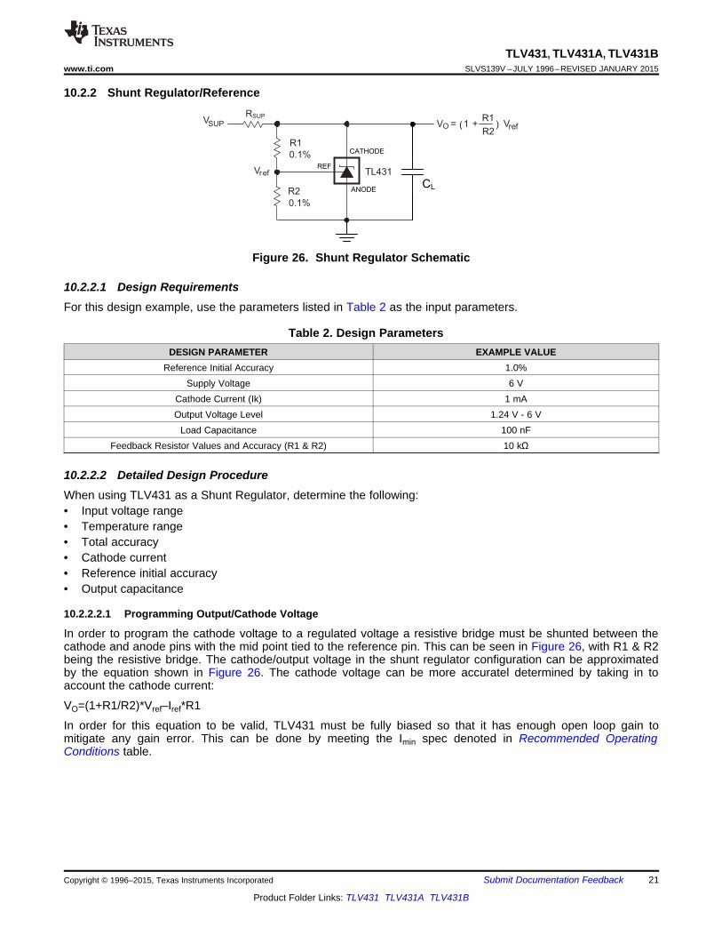
10.2.2 Shunt Regulator/Reference
Figure 26. Shunt Regulator Schematic
10.2.2.1 Design RequirementsFor this design example, use the parameters listed in Table 2 as the input parameters.
Table 2. Design ParametersDESIGN PARAMETER EXAMPLE VALUE
Reference Initial Accuracy 1.0%Supply Voltage 6 V
Cathode Current (Ik) 1 mAOutput Voltage Level 1.24 V - 6 V
Load Capacitance 100 nFFeedback Resistor Values and Accuracy (R1 & R2) 10 kΩ
10.2.2.2 Detailed Design ProcedureWhen using TLV431 as a Shunt Regulator, determine the following:• Input voltage range• Temperature range• Total accuracy• Cathode current• Reference initial accuracy• Output capacitance
10.2.2.2.1 Programming Output/Cathode Voltage
In order to program the cathode voltage to a regulated voltage a resistive bridge must be shunted between thecathode and anode pins with the mid point tied to the reference pin. This can be seen in Figure 26, with R1 & R2being the resistive bridge. The cathode/output voltage in the shunt regulator configuration can be approximatedby the equation shown in Figure 26. The cathode voltage can be more accuratel determined by taking in toaccount the cathode current:
VO=(1+R1/R2)*Vref–Iref*R1
In order for this equation to be valid, TLV431 must be fully biased so that it has enough open loop gain tomitigate any gain error. This can be done by meeting the Imin spec denoted in Recommended OperatingConditions table.
Copyright © 1996–2015, Texas Instruments Incorporated Submit Documentation Feedback 21
Product Folder Links: TLV431 TLV431A TLV431B
Time (Ps)
Vol
tage
(V
)
-1 0 1 2 3 4 5 6 7 8 9-0.5
00.5
11.5
22.5
33.5
44.5
55.5
66.5
D001
VsupVka=VrefR1=10k: & R2=10k:
TLV431, TLV431A, TLV431BSLVS139V –JULY 1996–REVISED JANUARY 2015 www.ti.com
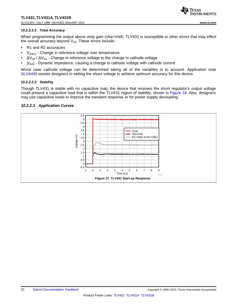
10.2.2.2.2 Total Accuracy
When programming the output above unity gain (Vka=Vref), TLV431 is susceptible to other errors that may effectthe overall accuracy beyond Vref. These errors include:
• R1 and R2 accuracies• VI(dev) - Change in reference voltage over temperature• ΔVref / ΔVKA - Change in reference voltage to the change in cathode voltage• |zKA| - Dynamic impedance, causing a change in cathode voltage with cathode current
Worst case cathode voltage can be determined taking all of the variables in to account. Application noteSLVA445 assists designers in setting the shunt voltage to achieve optimum accuracy for this device.
10.2.2.2.3 Stability
Though TLV431 is stable with no capacitive load, the device that receives the shunt regulator's output voltagecould present a capacitive load that is within the TLV431 region of stability, shown in Figure 18. Also, designersmay use capacitive loads to improve the transient response or for power supply decoupling.
10.2.2.3 Application Curves
Figure 27. TLV431 Start-up Response
22 Submit Documentation Feedback Copyright © 1996–2015, Texas Instruments Incorporated
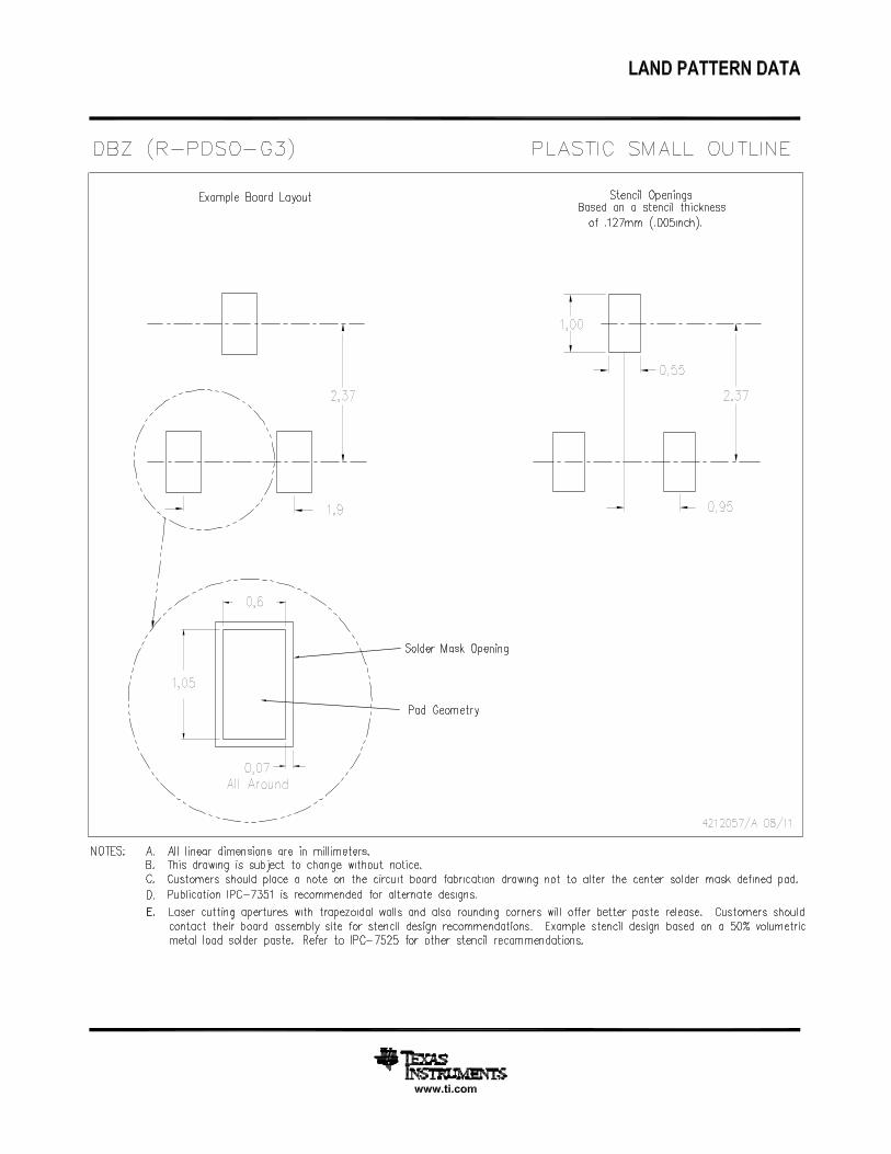
Product Folder Links: TLV431 TLV431A TLV431B
DBZ
(TOP VIEW)
REF
1
CATHODE
2
3ANODE
Rsup
Rref
Vsup
CL
Vin
GND
GND
TLV431, TLV431A, TLV431Bwww.ti.com SLVS139V –JULY 1996–REVISED JANUARY 2015
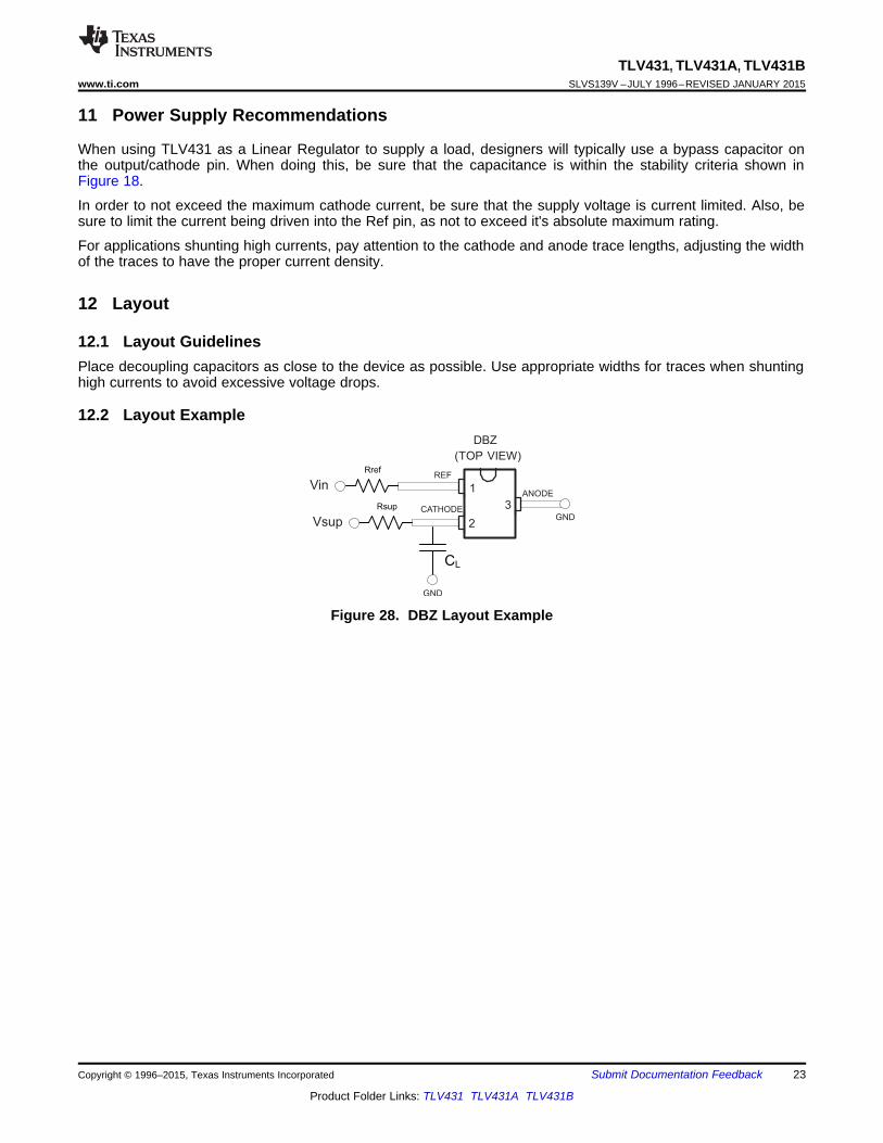
11 Power Supply Recommendations
When using TLV431 as a Linear Regulator to supply a load, designers will typically use a bypass capacitor onthe output/cathode pin. When doing this, be sure that the capacitance is within the stability criteria shown inFigure 18.
In order to not exceed the maximum cathode current, be sure that the supply voltage is current limited. Also, besure to limit the current being driven into the Ref pin, as not to exceed it's absolute maximum rating.
For applications shunting high currents, pay attention to the cathode and anode trace lengths, adjusting the widthof the traces to have the proper current density.
12 Layout
12.1 Layout GuidelinesPlace decoupling capacitors as close to the device as possible. Use appropriate widths for traces when shuntinghigh currents to avoid excessive voltage drops.
12.2 Layout Example
Figure 28. DBZ Layout Example
Copyright © 1996–2015, Texas Instruments Incorporated Submit Documentation Feedback 23
Product Folder Links: TLV431 TLV431A TLV431B
TLV431, TLV431A, TLV431BSLVS139V –JULY 1996–REVISED JANUARY 2015 www.ti.com
13 Device and Documentation Support
13.1 Related LinksThe table below lists quick access links. Categories include technical documents, support and communityresources, tools and software, and quick access to sample or buy.
Table 3. Related LinksTECHNICAL TOOLS & SUPPORT &PARTS PRODUCT FOLDER SAMPLE & BUY DOCUMENTS SOFTWARE COMMUNITY
TLV431 Click here Click here Click here Click here Click hereTLV431A Click here Click here Click here Click here Click hereTLV431B Click here Click here Click here Click here Click here
13.2 TrademarksAll trademarks are the property of their respective owners.
13.3 Electrostatic Discharge CautionThese devices have limited built-in ESD protection. The leads should be shorted together or the device placed in conductive foamduring storage or handling to prevent electrostatic damage to the MOS gates.
13.4 GlossarySLYZ022 — TI Glossary.
This glossary lists and explains terms, acronyms, and definitions.
14 Mechanical, Packaging, and Orderable InformationThe following pages include mechanical packaging and orderable information. This information is the mostcurrent data available for the designated devices. This data is subject to change without notice and revision ofthis document. For browser based versions of this data sheet, refer to the left hand navigation.
24 Submit Documentation Feedback Copyright © 1996–2015, Texas Instruments Incorporated
Product Folder Links: TLV431 TLV431A TLV431B
PACKAGE OPTION ADDENDUM
www.ti.com 18-Sep-2015
Addendum-Page 1
PACKAGING INFORMATION
Orderable Device Status(1)
Package Type PackageDrawing
Pins PackageQty
Eco Plan(2)
Lead/Ball Finish(6)
MSL Peak Temp(3)
Op Temp (°C) Device Marking(4/5)
Samples
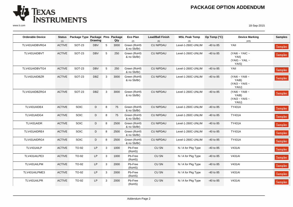
TLV431ACDBVR ACTIVE SOT-23 DBV 5 3000 Green (RoHS& no Sb/Br)
CU NIPDAU Level-1-260C-UNLIM 0 to 70 (YAC6 ~ YACC ~ YACI ~ YACN)(YACG ~ YACL ~ YACS)
TLV431ACDBVRG4 ACTIVE SOT-23 DBV 5 3000 Green (RoHS& no Sb/Br)
CU NIPDAU Level-1-260C-UNLIM 0 to 70 YACI
TLV431ACDBVT ACTIVE SOT-23 DBV 5 250 Green (RoHS& no Sb/Br)
CU NIPDAU Level-1-260C-UNLIM 0 to 70 (YAC6 ~ YACC ~ YACI)(YACG ~ YACL ~ YACS)
TLV431ACDBVTE4 ACTIVE SOT-23 DBV 5 TBD Call TI Call TI 0 to 70
TLV431ACDBVTG4 ACTIVE SOT-23 DBV 5 250 Green (RoHS& no Sb/Br)
CU NIPDAU Level-1-260C-UNLIM 0 to 70 YACI
TLV431ACDBZR ACTIVE SOT-23 DBZ 3 3000 Green (RoHS& no Sb/Br)
CU NIPDAU Level-1-260C-UNLIM 0 to 70 (YAC6 ~ YAC8 ~ YACB)(YAC3 ~ YACU)
TLV431ACDBZRG4 ACTIVE SOT-23 DBZ 3 3000 Green (RoHS& no Sb/Br)
CU NIPDAU Level-1-260C-UNLIM 0 to 70 (YAC6 ~ YAC8 ~ YACB)(YAC3 ~ YACU)
TLV431ACLP ACTIVE TO-92 LP 3 1000 Pb-Free(RoHS)
CU SN N / A for Pkg Type 0 to 70 V431AC
TLV431ACLPE3 ACTIVE TO-92 LP 3 1000 Pb-Free(RoHS)
CU SN N / A for Pkg Type 0 to 70 V431AC
TLV431ACLPR ACTIVE TO-92 LP 3 2000 Pb-Free(RoHS)
CU SN N / A for Pkg Type 0 to 70 V431AC
TLV431ACLPRE3 ACTIVE TO-92 LP 3 2000 Pb-Free(RoHS)
CU SN N / A for Pkg Type 0 to 70 V431AC
TLV431AID ACTIVE SOIC D 8 75 Green (RoHS& no Sb/Br)
CU NIPDAU Level-1-260C-UNLIM -40 to 85 TY431A
TLV431AIDBVR ACTIVE SOT-23 DBV 5 3000 Green (RoHS& no Sb/Br)
CU NIPDAU Level-1-260C-UNLIM -40 to 85 (YAI6 ~ YAIC ~ YAII ~ YAIN)(YAIG ~ YAIL ~ YAIS)
TLV431AIDBVRE4 ACTIVE SOT-23 DBV 5 3000 Green (RoHS& no Sb/Br)
CU NIPDAU Level-1-260C-UNLIM -40 to 85 YAII
PACKAGE OPTION ADDENDUM
www.ti.com 18-Sep-2015
Addendum-Page 2
Orderable Device Status(1)
Package Type PackageDrawing
Pins PackageQty
Eco Plan(2)
Lead/Ball Finish(6)
MSL Peak Temp(3)
Op Temp (°C) Device Marking(4/5)
Samples
TLV431AIDBVRG4 ACTIVE SOT-23 DBV 5 3000 Green (RoHS& no Sb/Br)
CU NIPDAU Level-1-260C-UNLIM -40 to 85 YAII
TLV431AIDBVT ACTIVE SOT-23 DBV 5 250 Green (RoHS& no Sb/Br)
CU NIPDAU Level-1-260C-UNLIM -40 to 85 (YAI6 ~ YAIC ~ YAII)(YAIG ~ YAIL ~ YAIS)
TLV431AIDBVTG4 ACTIVE SOT-23 DBV 5 250 Green (RoHS& no Sb/Br)
CU NIPDAU Level-1-260C-UNLIM -40 to 85 YAII
TLV431AIDBZR ACTIVE SOT-23 DBZ 3 3000 Green (RoHS& no Sb/Br)
CU NIPDAU Level-1-260C-UNLIM -40 to 85 (YAI6 ~ YAI8 ~ YAIB)(YAI3 ~ YAIS ~ YAIU)
TLV431AIDBZRG4 ACTIVE SOT-23 DBZ 3 3000 Green (RoHS& no Sb/Br)
CU NIPDAU Level-1-260C-UNLIM -40 to 85 (YAI6 ~ YAI8 ~ YAIB)(YAI3 ~ YAIS ~ YAIU)
TLV431AIDE4 ACTIVE SOIC D 8 75 Green (RoHS& no Sb/Br)
CU NIPDAU Level-1-260C-UNLIM -40 to 85 TY431A
TLV431AIDG4 ACTIVE SOIC D 8 75 Green (RoHS& no Sb/Br)
CU NIPDAU Level-1-260C-UNLIM -40 to 85 TY431A
TLV431AIDR ACTIVE SOIC D 8 2500 Green (RoHS& no Sb/Br)
CU NIPDAU Level-1-260C-UNLIM -40 to 85 TY431A
TLV431AIDRE4 ACTIVE SOIC D 8 2500 Green (RoHS& no Sb/Br)
CU NIPDAU Level-1-260C-UNLIM -40 to 85 TY431A
TLV431AIDRG4 ACTIVE SOIC D 8 2500 Green (RoHS& no Sb/Br)
CU NIPDAU Level-1-260C-UNLIM -40 to 85 TY431A
TLV431AILP ACTIVE TO-92 LP 3 1000 Pb-Free(RoHS)
CU SN N / A for Pkg Type -40 to 85 V431AI
TLV431AILPE3 ACTIVE TO-92 LP 3 1000 Pb-Free(RoHS)
CU SN N / A for Pkg Type -40 to 85 V431AI
TLV431AILPM ACTIVE TO-92 LP 3 2000 Pb-Free(RoHS)
CU SN N / A for Pkg Type -40 to 85 V431AI
TLV431AILPME3 ACTIVE TO-92 LP 3 2000 Pb-Free(RoHS)
CU SN N / A for Pkg Type -40 to 85 V431AI
TLV431AILPR ACTIVE TO-92 LP 3 2000 Pb-Free(RoHS)
CU SN N / A for Pkg Type -40 to 85 V431AI

PACKAGE OPTION ADDENDUM
www.ti.com 18-Sep-2015
Addendum-Page 3
Orderable Device Status(1)
Package Type PackageDrawing
Pins PackageQty
Eco Plan(2)
Lead/Ball Finish(6)
MSL Peak Temp(3)
Op Temp (°C) Device Marking(4/5)
Samples
TLV431AILPRE3 ACTIVE TO-92 LP 3 2000 Pb-Free(RoHS)
CU SN N / A for Pkg Type -40 to 85 V431AI
TLV431AQPK ACTIVE SOT-89 PK 3 1000 Green (RoHS& no Sb/Br)
CU SN Level-2-260C-1 YEAR -40 to 125 VA
TLV431AQPKG3 ACTIVE SOT-89 PK 3 1000 Green (RoHS& no Sb/Br)
CU SN Level-2-260C-1 YEAR -40 to 125 VA
TLV431BCDBVR ACTIVE SOT-23 DBV 5 3000 Green (RoHS& no Sb/Br)
CU NIPDAU | CU SN Level-1-260C-UNLIM 0 to 70 (Y3GG ~ Y3GU)
TLV431BCDBVRG4 ACTIVE SOT-23 DBV 5 3000 Green (RoHS& no Sb/Br)
CU NIPDAU Level-1-260C-UNLIM 0 to 70 Y3GG
TLV431BCDBVT ACTIVE SOT-23 DBV 5 250 Green (RoHS& no Sb/Br)
CU NIPDAU | CU SN Level-1-260C-UNLIM 0 to 70 (Y3GG ~ Y3GU)
TLV431BCDBVTG4 ACTIVE SOT-23 DBV 5 250 Green (RoHS& no Sb/Br)
CU NIPDAU Level-1-260C-UNLIM 0 to 70 Y3GG
TLV431BCDBZR ACTIVE SOT-23 DBZ 3 3000 Green (RoHS& no Sb/Br)
CU NIPDAU Level-1-260C-UNLIM 0 to 70 (Y3G3 ~ Y3GS ~ Y3GU)
TLV431BCDBZRG4 ACTIVE SOT-23 DBZ 3 3000 Green (RoHS& no Sb/Br)
CU NIPDAU Level-1-260C-UNLIM 0 to 70 (Y3G3 ~ Y3GS ~ Y3GU)
TLV431BCDBZT ACTIVE SOT-23 DBZ 3 250 Green (RoHS& no Sb/Br)
CU NIPDAU Level-1-260C-UNLIM 0 to 70 (Y3GS ~ Y3GU)
TLV431BCDBZTG4 ACTIVE SOT-23 DBZ 3 250 Green (RoHS& no Sb/Br)
CU NIPDAU Level-1-260C-UNLIM 0 to 70 (Y3GS ~ Y3GU)
TLV431BCDCKR ACTIVE SC70 DCK 6 3000 Green (RoHS& no Sb/Br)
CU NIPDAU Level-1-260C-UNLIM 0 to 70 YEU
TLV431BCDCKT ACTIVE SC70 DCK 6 250 Green (RoHS& no Sb/Br)
CU NIPDAU Level-1-260C-UNLIM 0 to 70 YEU
TLV431BCLP ACTIVE TO-92 LP 3 1000 Pb-Free(RoHS)
CU SN N / A for Pkg Type 0 to 70 TV431B
TLV431BCLPR ACTIVE TO-92 LP 3 2000 Pb-Free(RoHS)
CU SN N / A for Pkg Type 0 to 70 TV431B
TLV431BCLPRE3 ACTIVE TO-92 LP 3 2000 Pb-Free(RoHS)
CU SN N / A for Pkg Type 0 to 70 TV431B
TLV431BCPK ACTIVE SOT-89 PK 3 1000 Green (RoHS& no Sb/Br)
CU SN Level-2-260C-1 YEAR 0 to 70 VE
TLV431BIDBVR ACTIVE SOT-23 DBV 5 3000 Green (RoHS& no Sb/Br)
CU NIPDAU Level-1-260C-UNLIM -40 to 85 Y3FU
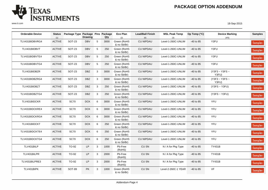
PACKAGE OPTION ADDENDUM
www.ti.com 18-Sep-2015
Addendum-Page 4
Orderable Device Status(1)
Package Type PackageDrawing
Pins PackageQty
Eco Plan(2)
Lead/Ball Finish(6)
MSL Peak Temp(3)
Op Temp (°C) Device Marking(4/5)
Samples
TLV431BIDBVRG4 ACTIVE SOT-23 DBV 5 3000 Green (RoHS& no Sb/Br)
CU NIPDAU Level-1-260C-UNLIM -40 to 85 Y3FU
TLV431BIDBVT ACTIVE SOT-23 DBV 5 250 Green (RoHS& no Sb/Br)
CU NIPDAU Level-1-260C-UNLIM -40 to 85 Y3FU
TLV431BIDBVTE4 ACTIVE SOT-23 DBV 5 250 Green (RoHS& no Sb/Br)
CU NIPDAU Level-1-260C-UNLIM -40 to 85 Y3FU
TLV431BIDBVTG4 ACTIVE SOT-23 DBV 5 250 Green (RoHS& no Sb/Br)
CU NIPDAU Level-1-260C-UNLIM -40 to 85 Y3FU
TLV431BIDBZR ACTIVE SOT-23 DBZ 3 3000 Green (RoHS& no Sb/Br)
CU NIPDAU Level-1-260C-UNLIM -40 to 85 (Y3F3 ~ Y3FS ~ Y3FU)
TLV431BIDBZRG4 ACTIVE SOT-23 DBZ 3 3000 Green (RoHS& no Sb/Br)
CU NIPDAU Level-1-260C-UNLIM -40 to 85 (Y3F3 ~ Y3FS ~ Y3FU)
TLV431BIDBZT ACTIVE SOT-23 DBZ 3 250 Green (RoHS& no Sb/Br)
CU NIPDAU Level-1-260C-UNLIM -40 to 85 (Y3FS ~ Y3FU)
TLV431BIDBZTG4 ACTIVE SOT-23 DBZ 3 250 Green (RoHS& no Sb/Br)
CU NIPDAU Level-1-260C-UNLIM -40 to 85 (Y3FS ~ Y3FU)
TLV431BIDCKR ACTIVE SC70 DCK 6 3000 Green (RoHS& no Sb/Br)
CU NIPDAU Level-1-260C-UNLIM -40 to 85 YFU
TLV431BIDCKRE4 ACTIVE SC70 DCK 6 3000 Green (RoHS& no Sb/Br)
CU NIPDAU Level-1-260C-UNLIM -40 to 85 YFU
TLV431BIDCKRG4 ACTIVE SC70 DCK 6 3000 Green (RoHS& no Sb/Br)
CU NIPDAU Level-1-260C-UNLIM -40 to 85 YFU
TLV431BIDCKT ACTIVE SC70 DCK 6 250 Green (RoHS& no Sb/Br)
CU NIPDAU Level-1-260C-UNLIM -40 to 85 YFU
TLV431BIDCKTE4 ACTIVE SC70 DCK 6 250 Green (RoHS& no Sb/Br)
CU NIPDAU Level-1-260C-UNLIM -40 to 85 YFU
TLV431BIDCKTG4 ACTIVE SC70 DCK 6 250 Green (RoHS& no Sb/Br)
CU NIPDAU Level-1-260C-UNLIM -40 to 85 YFU
TLV431BILP ACTIVE TO-92 LP 3 1000 Pb-Free(RoHS)
CU SN N / A for Pkg Type -40 to 85 TY431B
TLV431BILPR ACTIVE TO-92 LP 3 2000 Pb-Free(RoHS)
CU SN N / A for Pkg Type -40 to 85 TY431B
TLV431BILPRE3 ACTIVE TO-92 LP 3 2000 Pb-Free(RoHS)
CU SN N / A for Pkg Type -40 to 85 TY431B
TLV431BIPK ACTIVE SOT-89 PK 3 1000 Green (RoHS& no Sb/Br)
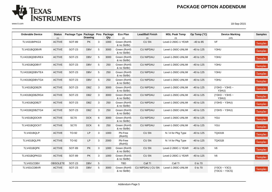
CU SN Level-2-260C-1 YEAR -40 to 85 VF
PACKAGE OPTION ADDENDUM
www.ti.com 18-Sep-2015
Addendum-Page 5
Orderable Device Status(1)
Package Type PackageDrawing
Pins PackageQty
Eco Plan(2)
Lead/Ball Finish(6)
MSL Peak Temp(3)
Op Temp (°C) Device Marking(4/5)
Samples
TLV431BIPKG3 ACTIVE SOT-89 PK 3 1000 Green (RoHS& no Sb/Br)
CU SN Level-2-260C-1 YEAR -40 to 85 VF
TLV431BQDBVR ACTIVE SOT-23 DBV 5 3000 Green (RoHS& no Sb/Br)
CU NIPDAU Level-1-260C-UNLIM -40 to 125 Y3HU
TLV431BQDBVRE4 ACTIVE SOT-23 DBV 5 3000 Green (RoHS& no Sb/Br)
CU NIPDAU Level-1-260C-UNLIM -40 to 125 Y3HU
TLV431BQDBVT ACTIVE SOT-23 DBV 5 250 Green (RoHS& no Sb/Br)
CU NIPDAU Level-1-260C-UNLIM -40 to 125 Y3HU
TLV431BQDBVTE4 ACTIVE SOT-23 DBV 5 250 Green (RoHS& no Sb/Br)
CU NIPDAU Level-1-260C-UNLIM -40 to 125 Y3HU
TLV431BQDBVTG4 ACTIVE SOT-23 DBV 5 250 Green (RoHS& no Sb/Br)
CU NIPDAU Level-1-260C-UNLIM -40 to 125 Y3HU
TLV431BQDBZR ACTIVE SOT-23 DBZ 3 3000 Green (RoHS& no Sb/Br)
CU NIPDAU Level-1-260C-UNLIM -40 to 125 (Y3H3 ~ Y3HS ~ Y3HU)
TLV431BQDBZRG4 ACTIVE SOT-23 DBZ 3 3000 Green (RoHS& no Sb/Br)
CU NIPDAU Level-1-260C-UNLIM -40 to 125 (Y3H3 ~ Y3HS ~ Y3HU)
TLV431BQDBZT ACTIVE SOT-23 DBZ 3 250 Green (RoHS& no Sb/Br)
CU NIPDAU Level-1-260C-UNLIM -40 to 125 (Y3HS ~ Y3HU)
TLV431BQDBZTG4 ACTIVE SOT-23 DBZ 3 250 Green (RoHS& no Sb/Br)
CU NIPDAU Level-1-260C-UNLIM -40 to 125 (Y3HS ~ Y3HU)
TLV431BQDCKR ACTIVE SC70 DCK 6 3000 Green (RoHS& no Sb/Br)
CU NIPDAU Level-1-260C-UNLIM -40 to 125 YGU
TLV431BQDCKT ACTIVE SC70 DCK 6 250 Green (RoHS& no Sb/Br)
CU NIPDAU Level-1-260C-UNLIM -40 to 125 YGU
TLV431BQLP ACTIVE TO-92 LP 3 1000 Pb-Free(RoHS)
CU SN N / A for Pkg Type -40 to 125 TQ431B
TLV431BQLPR ACTIVE TO-92 LP 3 2000 Pb-Free(RoHS)
CU SN N / A for Pkg Type -40 to 125 TQ431B
TLV431BQPK ACTIVE SOT-89 PK 3 1000 Green (RoHS& no Sb/Br)
CU SN Level-2-260C-1 YEAR -40 to 125 V6
TLV431BQPKG3 ACTIVE SOT-89 PK 3 1000 Green (RoHS& no Sb/Br)
CU SN Level-2-260C-1 YEAR -40 to 125 V6
TLV431CDBV OBSOLETE SOT-23 DBV 5 TBD Call TI Call TI 0 to 70
TLV431CDBVR ACTIVE SOT-23 DBV 5 3000 Green (RoHS& no Sb/Br)
CU NIPDAU | CU SN Level-1-260C-UNLIM 0 to 70 (Y3C6 ~ Y3CI)(Y3CG ~ Y3CS)
PACKAGE OPTION ADDENDUM
www.ti.com 18-Sep-2015
Addendum-Page 6
Orderable Device Status(1)
Package Type PackageDrawing
Pins PackageQty
Eco Plan(2)
Lead/Ball Finish(6)
MSL Peak Temp(3)
Op Temp (°C) Device Marking(4/5)
Samples
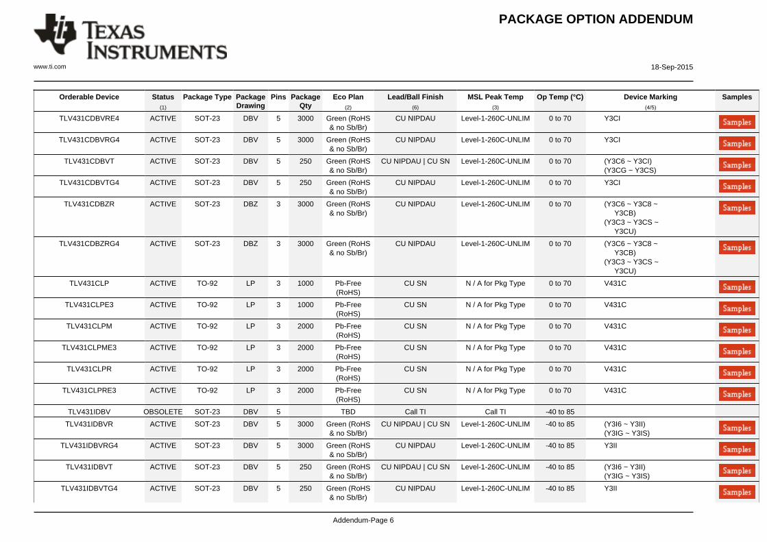
TLV431CDBVRE4 ACTIVE SOT-23 DBV 5 3000 Green (RoHS& no Sb/Br)
CU NIPDAU Level-1-260C-UNLIM 0 to 70 Y3CI
TLV431CDBVRG4 ACTIVE SOT-23 DBV 5 3000 Green (RoHS& no Sb/Br)
CU NIPDAU Level-1-260C-UNLIM 0 to 70 Y3CI
TLV431CDBVT ACTIVE SOT-23 DBV 5 250 Green (RoHS& no Sb/Br)
CU NIPDAU | CU SN Level-1-260C-UNLIM 0 to 70 (Y3C6 ~ Y3CI)(Y3CG ~ Y3CS)
TLV431CDBVTG4 ACTIVE SOT-23 DBV 5 250 Green (RoHS& no Sb/Br)
CU NIPDAU Level-1-260C-UNLIM 0 to 70 Y3CI
TLV431CDBZR ACTIVE SOT-23 DBZ 3 3000 Green (RoHS& no Sb/Br)
CU NIPDAU Level-1-260C-UNLIM 0 to 70 (Y3C6 ~ Y3C8 ~ Y3CB)(Y3C3 ~ Y3CS ~ Y3CU)
TLV431CDBZRG4 ACTIVE SOT-23 DBZ 3 3000 Green (RoHS& no Sb/Br)
CU NIPDAU Level-1-260C-UNLIM 0 to 70 (Y3C6 ~ Y3C8 ~ Y3CB)(Y3C3 ~ Y3CS ~ Y3CU)
TLV431CLP ACTIVE TO-92 LP 3 1000 Pb-Free(RoHS)
CU SN N / A for Pkg Type 0 to 70 V431C
TLV431CLPE3 ACTIVE TO-92 LP 3 1000 Pb-Free(RoHS)
CU SN N / A for Pkg Type 0 to 70 V431C
TLV431CLPM ACTIVE TO-92 LP 3 2000 Pb-Free(RoHS)
CU SN N / A for Pkg Type 0 to 70 V431C
TLV431CLPME3 ACTIVE TO-92 LP 3 2000 Pb-Free(RoHS)
CU SN N / A for Pkg Type 0 to 70 V431C
TLV431CLPR ACTIVE TO-92 LP 3 2000 Pb-Free(RoHS)
CU SN N / A for Pkg Type 0 to 70 V431C
TLV431CLPRE3 ACTIVE TO-92 LP 3 2000 Pb-Free(RoHS)
CU SN N / A for Pkg Type 0 to 70 V431C
TLV431IDBV OBSOLETE SOT-23 DBV 5 TBD Call TI Call TI -40 to 85
TLV431IDBVR ACTIVE SOT-23 DBV 5 3000 Green (RoHS& no Sb/Br)
CU NIPDAU | CU SN Level-1-260C-UNLIM -40 to 85 (Y3I6 ~ Y3II)(Y3IG ~ Y3IS)
TLV431IDBVRG4 ACTIVE SOT-23 DBV 5 3000 Green (RoHS& no Sb/Br)
CU NIPDAU Level-1-260C-UNLIM -40 to 85 Y3II
TLV431IDBVT ACTIVE SOT-23 DBV 5 250 Green (RoHS& no Sb/Br)
CU NIPDAU | CU SN Level-1-260C-UNLIM -40 to 85 (Y3I6 ~ Y3II)(Y3IG ~ Y3IS)
TLV431IDBVTG4 ACTIVE SOT-23 DBV 5 250 Green (RoHS& no Sb/Br)
CU NIPDAU Level-1-260C-UNLIM -40 to 85 Y3II
PACKAGE OPTION ADDENDUM
www.ti.com 18-Sep-2015
Addendum-Page 7
Orderable Device Status(1)
Package Type PackageDrawing
Pins PackageQty
Eco Plan(2)
Lead/Ball Finish(6)
MSL Peak Temp(3)
Op Temp (°C) Device Marking(4/5)
Samples
TLV431IDBZR ACTIVE SOT-23 DBZ 3 3000 Green (RoHS& no Sb/Br)
CU NIPDAU Level-1-260C-UNLIM -40 to 85 (Y3I6 ~ Y3IB)(Y3IS ~ Y3IU)
TLV431IDBZRG4 ACTIVE SOT-23 DBZ 3 3000 Green (RoHS& no Sb/Br)
CU NIPDAU Level-1-260C-UNLIM -40 to 85 (Y3I6 ~ Y3IB)(Y3IS ~ Y3IU)
TLV431ILP ACTIVE TO-92 LP 3 1000 Pb-Free(RoHS)
CU SN N / A for Pkg Type -40 to 85 V431I
TLV431ILPE3 ACTIVE TO-92 LP 3 1000 Pb-Free(RoHS)
CU SN N / A for Pkg Type -40 to 85 V431I
TLV431ILPR ACTIVE TO-92 LP 3 2000 Pb-Free(RoHS)
CU SN N / A for Pkg Type -40 to 85 V431I
TLV431QPK ACTIVE SOT-89 PK 3 1000 Green (RoHS& no Sb/Br)
CU SN Level-2-260C-1 YEAR -40 to 125 VB
TLV431QPKG3 ACTIVE SOT-89 PK 3 1000 Green (RoHS& no Sb/Br)
CU SN Level-2-260C-1 YEAR -40 to 125 VB
(1) The marketing status values are defined as follows:ACTIVE: Product device recommended for new designs.LIFEBUY: TI has announced that the device will be discontinued, and a lifetime-buy period is in effect.NRND: Not recommended for new designs. Device is in production to support existing customers, but TI does not recommend using this part in a new design.PREVIEW: Device has been announced but is not in production. Samples may or may not be available.OBSOLETE: TI has discontinued the production of the device.
(2) Eco Plan - The planned eco-friendly classification: Pb-Free (RoHS), Pb-Free (RoHS Exempt), or Green (RoHS & no Sb/Br) - please check http://www.ti.com/productcontent for the latest availabilityinformation and additional product content details.TBD: The Pb-Free/Green conversion plan has not been defined.Pb-Free (RoHS): TI's terms "Lead-Free" or "Pb-Free" mean semiconductor products that are compatible with the current RoHS requirements for all 6 substances, including the requirement thatlead not exceed 0.1% by weight in homogeneous materials. Where designed to be soldered at high temperatures, TI Pb-Free products are suitable for use in specified lead-free processes.Pb-Free (RoHS Exempt): This component has a RoHS exemption for either 1) lead-based flip-chip solder bumps used between the die and package, or 2) lead-based die adhesive used betweenthe die and leadframe. The component is otherwise considered Pb-Free (RoHS compatible) as defined above.Green (RoHS & no Sb/Br): TI defines "Green" to mean Pb-Free (RoHS compatible), and free of Bromine (Br) and Antimony (Sb) based flame retardants (Br or Sb do not exceed 0.1% by weightin homogeneous material)
(3) MSL, Peak Temp. - The Moisture Sensitivity Level rating according to the JEDEC industry standard classifications, and peak solder temperature.
(4) There may be additional marking, which relates to the logo, the lot trace code information, or the environmental category on the device.
(5) Multiple Device Markings will be inside parentheses. Only one Device Marking contained in parentheses and separated by a "~" will appear on a device. If a line is indented then it is a continuationof the previous line and the two combined represent the entire Device Marking for that device.
PACKAGE OPTION ADDENDUM
www.ti.com 18-Sep-2015
Addendum-Page 8
(6) Lead/Ball Finish - Orderable Devices may have multiple material finish options. Finish options are separated by a vertical ruled line. Lead/Ball Finish values may wrap to two lines if the finishvalue exceeds the maximum column width.
Important Information and Disclaimer:The information provided on this page represents TI's knowledge and belief as of the date that it is provided. TI bases its knowledge and belief on informationprovided by third parties, and makes no representation or warranty as to the accuracy of such information. Efforts are underway to better integrate information from third parties. TI has taken andcontinues to take reasonable steps to provide representative and accurate information but may not have conducted destructive testing or chemical analysis on incoming materials and chemicals.TI and TI suppliers consider certain information to be proprietary, and thus CAS numbers and other limited information may not be available for release.
In no event shall TI's liability arising out of such information exceed the total purchase price of the TI part(s) at issue in this document sold by TI to Customer on an annual basis.
OTHER QUALIFIED VERSIONS OF TLV431A, TLV431B :
• Automotive: TLV431A-Q1, TLV431B-Q1
NOTE: Qualified Version Definitions:
• Automotive - Q100 devices qualified for high-reliability automotive applications targeting zero defects
TAPE AND REEL INFORMATION
*All dimensions are nominal
Device PackageType
PackageDrawing
Pins SPQ ReelDiameter
(mm)
ReelWidth
W1 (mm)
A0(mm)
B0(mm)
K0(mm)
P1(mm)
W(mm)
Pin1Quadrant
TLV431ACDBVR SOT-23 DBV 5 3000 180.0 9.2 3.17 3.23 1.37 4.0 8.0 Q3
TLV431ACDBVR SOT-23 DBV 5 3000 178.0 9.0 3.23 3.17 1.37 4.0 8.0 Q3
TLV431ACDBVRG4 SOT-23 DBV 5 3000 178.0 9.0 3.23 3.17 1.37 4.0 8.0 Q3
TLV431ACDBVT SOT-23 DBV 5 250 180.0 9.2 3.17 3.23 1.37 4.0 8.0 Q3
TLV431ACDBVT SOT-23 DBV 5 250 178.0 9.0 3.23 3.17 1.37 4.0 8.0 Q3
TLV431ACDBVTG4 SOT-23 DBV 5 250 178.0 9.0 3.23 3.17 1.37 4.0 8.0 Q3
TLV431ACDBZR SOT-23 DBZ 3 3000 180.0 8.4 3.15 2.77 1.22 4.0 8.0 Q3
TLV431AIDBVR SOT-23 DBV 5 3000 178.0 9.0 3.23 3.17 1.37 4.0 8.0 Q3
TLV431AIDBVRG4 SOT-23 DBV 5 3000 178.0 9.0 3.23 3.17 1.37 4.0 8.0 Q3
TLV431AIDBVT SOT-23 DBV 5 250 178.0 9.0 3.23 3.17 1.37 4.0 8.0 Q3
TLV431AIDBVT SOT-23 DBV 5 250 180.0 9.2 3.17 3.23 1.37 4.0 8.0 Q3
TLV431AIDBVTG4 SOT-23 DBV 5 250 178.0 9.0 3.23 3.17 1.37 4.0 8.0 Q3
TLV431AIDBZR SOT-23 DBZ 3 3000 180.0 8.4 3.15 2.77 1.22 4.0 8.0 Q3
TLV431AIDR SOIC D 8 2500 330.0 12.4 6.4 5.2 2.1 8.0 12.0 Q1
TLV431AQPK SOT-89 PK 3 1000 180.0 12.4 4.91 4.52 1.9 8.0 12.0 Q3
TLV431BCDBVR SOT-23 DBV 5 3000 178.0 9.0 3.23 3.17 1.37 4.0 8.0 Q3
TLV431BCDBVRG4 SOT-23 DBV 5 3000 178.0 9.0 3.23 3.17 1.37 4.0 8.0 Q3
TLV431BCDBVT SOT-23 DBV 5 250 178.0 9.0 3.23 3.17 1.37 4.0 8.0 Q3
PACKAGE MATERIALS INFORMATION
www.ti.com 23-Oct-2015
Pack Materials-Page 1
Device PackageType
PackageDrawing
Pins SPQ ReelDiameter
(mm)
ReelWidth
W1 (mm)
A0(mm)
B0(mm)
K0(mm)
P1(mm)
W(mm)
Pin1Quadrant
TLV431BCDBVTG4 SOT-23 DBV 5 250 178.0 9.0 3.23 3.17 1.37 4.0 8.0 Q3
TLV431BCDBZR SOT-23 DBZ 3 3000 180.0 8.4 3.15 2.77 1.22 4.0 8.0 Q3
TLV431BCDBZT SOT-23 DBZ 3 250 180.0 8.4 3.15 2.77 1.22 4.0 8.0 Q3
TLV431BCDCKR SC70 DCK 6 3000 179.0 8.4 2.2 2.5 1.2 4.0 8.0 Q3
TLV431BCDCKT SC70 DCK 6 250 179.0 8.4 2.2 2.5 1.2 4.0 8.0 Q3
TLV431BCPK SOT-89 PK 3 1000 180.0 12.4 4.91 4.52 1.9 8.0 12.0 Q3
TLV431BIDBVR SOT-23 DBV 5 3000 179.0 8.4 3.2 3.2 1.4 4.0 8.0 Q3
TLV431BIDBVT SOT-23 DBV 5 250 179.0 8.4 3.2 3.2 1.4 4.0 8.0 Q3
TLV431BIDBZR SOT-23 DBZ 3 3000 180.0 8.4 3.15 2.77 1.22 4.0 8.0 Q3
TLV431BIDBZT SOT-23 DBZ 3 250 180.0 8.4 3.15 2.77 1.22 4.0 8.0 Q3
TLV431BIDCKR SC70 DCK 6 3000 179.0 8.4 2.2 2.5 1.2 4.0 8.0 Q3
TLV431BIDCKT SC70 DCK 6 250 179.0 8.4 2.2 2.5 1.2 4.0 8.0 Q3
TLV431BIPK SOT-89 PK 3 1000 180.0 12.4 4.91 4.52 1.9 8.0 12.0 Q3
TLV431BQDBVR SOT-23 DBV 5 3000 179.0 8.4 3.2 3.2 1.4 4.0 8.0 Q3
TLV431BQDBVT SOT-23 DBV 5 250 179.0 8.4 3.2 3.2 1.4 4.0 8.0 Q3
TLV431BQDBZR SOT-23 DBZ 3 3000 180.0 8.4 3.15 2.77 1.22 4.0 8.0 Q3
TLV431BQDBZT SOT-23 DBZ 3 250 180.0 8.4 3.15 2.77 1.22 4.0 8.0 Q3
TLV431BQDCKR SC70 DCK 6 3000 179.0 8.4 2.2 2.5 1.2 4.0 8.0 Q3
TLV431BQDCKT SC70 DCK 6 250 179.0 8.4 2.2 2.5 1.2 4.0 8.0 Q3
TLV431BQPK SOT-89 PK 3 1000 180.0 12.4 4.91 4.52 1.9 8.0 12.0 Q3
TLV431CDBVR SOT-23 DBV 5 3000 178.0 9.0 3.23 3.17 1.37 4.0 8.0 Q3
TLV431CDBVRG4 SOT-23 DBV 5 3000 178.0 9.0 3.23 3.17 1.37 4.0 8.0 Q3
TLV431CDBVT SOT-23 DBV 5 250 180.0 8.4 3.23 3.17 1.37 4.0 8.0 Q3
TLV431CDBVTG4 SOT-23 DBV 5 250 178.0 9.0 3.23 3.17 1.37 4.0 8.0 Q3
TLV431CDBZR SOT-23 DBZ 3 3000 180.0 8.4 3.15 2.77 1.22 4.0 8.0 Q3
TLV431IDBVR SOT-23 DBV 5 3000 178.0 9.0 3.3 3.2 1.4 4.0 8.0 Q3
TLV431IDBVRG4 SOT-23 DBV 5 3000 178.0 9.0 3.3 3.2 1.4 4.0 8.0 Q3
TLV431IDBVT SOT-23 DBV 5 250 178.0 9.0 3.23 3.17 1.37 4.0 8.0 Q3
TLV431IDBVTG4 SOT-23 DBV 5 250 178.0 9.0 3.23 3.17 1.37 4.0 8.0 Q3
TLV431IDBZR SOT-23 DBZ 3 3000 180.0 8.4 3.15 2.77 1.22 4.0 8.0 Q3
TLV431QPK SOT-89 PK 3 1000 180.0 12.4 4.91 4.52 1.9 8.0 12.0 Q3
PACKAGE MATERIALS INFORMATION
www.ti.com 23-Oct-2015
Pack Materials-Page 2
*All dimensions are nominal
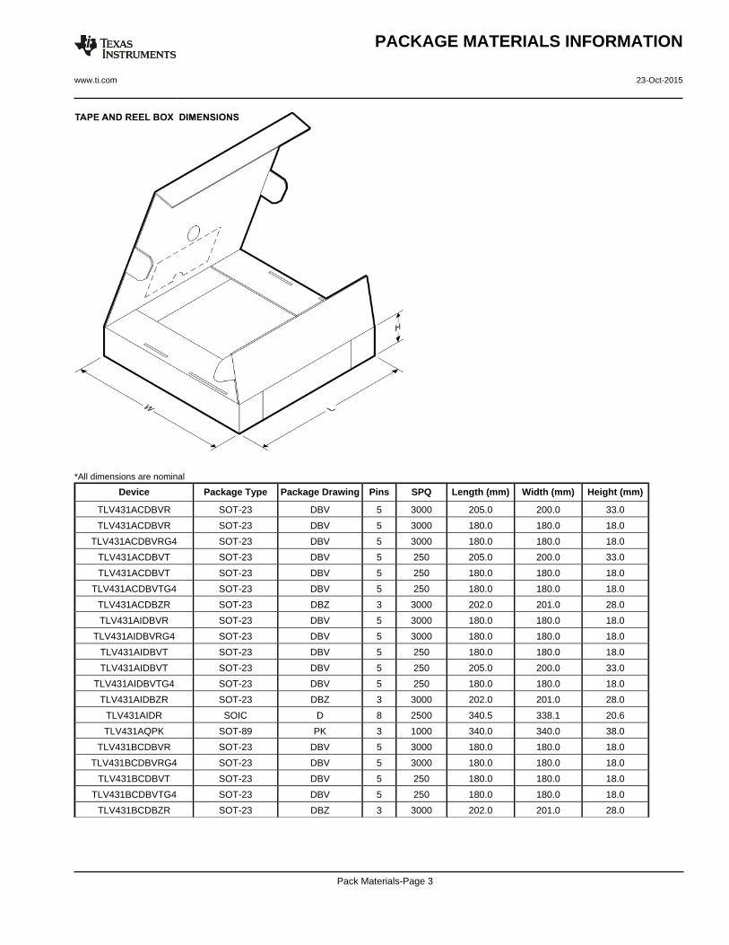
Device Package Type Package Drawing Pins SPQ Length (mm) Width (mm) Height (mm)
TLV431ACDBVR SOT-23 DBV 5 3000 205.0 200.0 33.0
TLV431ACDBVR SOT-23 DBV 5 3000 180.0 180.0 18.0
TLV431ACDBVRG4 SOT-23 DBV 5 3000 180.0 180.0 18.0
TLV431ACDBVT SOT-23 DBV 5 250 205.0 200.0 33.0
TLV431ACDBVT SOT-23 DBV 5 250 180.0 180.0 18.0
TLV431ACDBVTG4 SOT-23 DBV 5 250 180.0 180.0 18.0
TLV431ACDBZR SOT-23 DBZ 3 3000 202.0 201.0 28.0
TLV431AIDBVR SOT-23 DBV 5 3000 180.0 180.0 18.0
TLV431AIDBVRG4 SOT-23 DBV 5 3000 180.0 180.0 18.0
TLV431AIDBVT SOT-23 DBV 5 250 180.0 180.0 18.0
TLV431AIDBVT SOT-23 DBV 5 250 205.0 200.0 33.0
TLV431AIDBVTG4 SOT-23 DBV 5 250 180.0 180.0 18.0
TLV431AIDBZR SOT-23 DBZ 3 3000 202.0 201.0 28.0
TLV431AIDR SOIC D 8 2500 340.5 338.1 20.6
TLV431AQPK SOT-89 PK 3 1000 340.0 340.0 38.0
TLV431BCDBVR SOT-23 DBV 5 3000 180.0 180.0 18.0
TLV431BCDBVRG4 SOT-23 DBV 5 3000 180.0 180.0 18.0
TLV431BCDBVT SOT-23 DBV 5 250 180.0 180.0 18.0
TLV431BCDBVTG4 SOT-23 DBV 5 250 180.0 180.0 18.0
TLV431BCDBZR SOT-23 DBZ 3 3000 202.0 201.0 28.0
PACKAGE MATERIALS INFORMATION
www.ti.com 23-Oct-2015
Pack Materials-Page 3
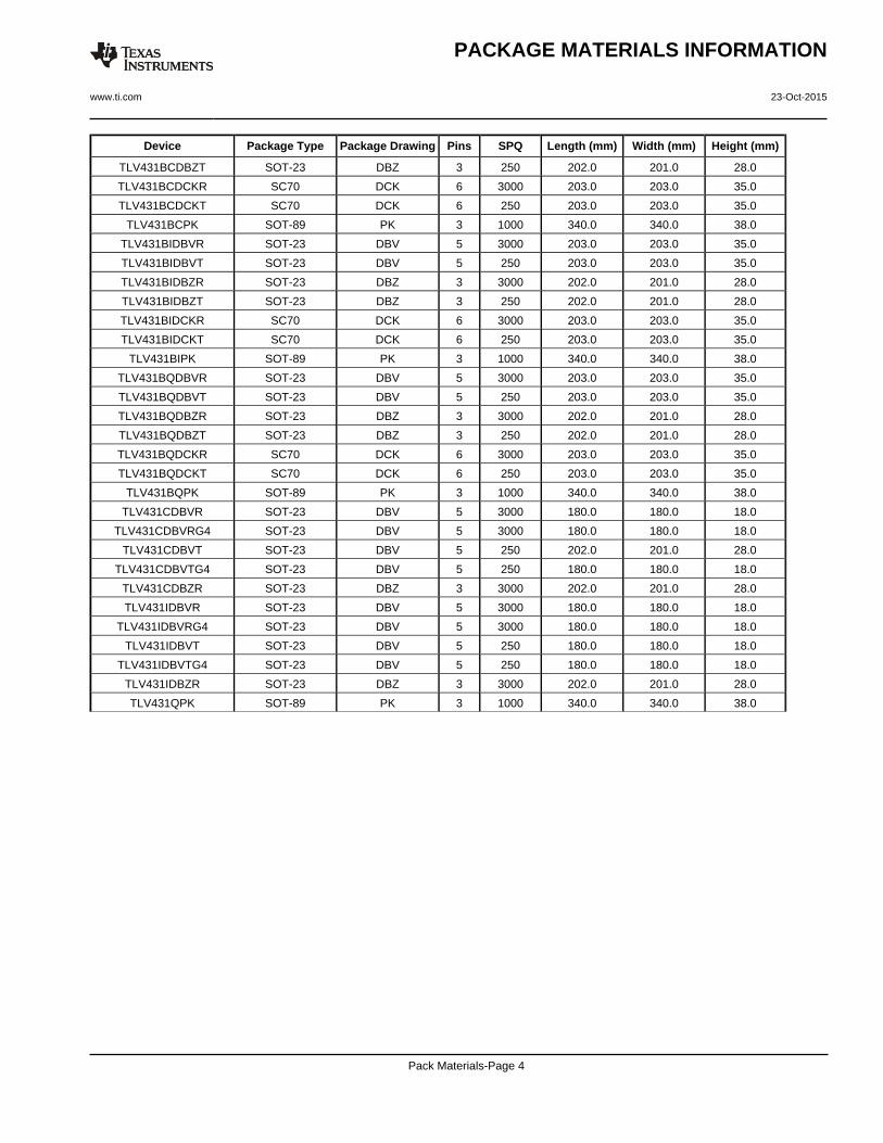
Device Package Type Package Drawing Pins SPQ Length (mm) Width (mm) Height (mm)
TLV431BCDBZT SOT-23 DBZ 3 250 202.0 201.0 28.0
TLV431BCDCKR SC70 DCK 6 3000 203.0 203.0 35.0
TLV431BCDCKT SC70 DCK 6 250 203.0 203.0 35.0
TLV431BCPK SOT-89 PK 3 1000 340.0 340.0 38.0
TLV431BIDBVR SOT-23 DBV 5 3000 203.0 203.0 35.0
TLV431BIDBVT SOT-23 DBV 5 250 203.0 203.0 35.0
TLV431BIDBZR SOT-23 DBZ 3 3000 202.0 201.0 28.0
TLV431BIDBZT SOT-23 DBZ 3 250 202.0 201.0 28.0
TLV431BIDCKR SC70 DCK 6 3000 203.0 203.0 35.0
TLV431BIDCKT SC70 DCK 6 250 203.0 203.0 35.0
TLV431BIPK SOT-89 PK 3 1000 340.0 340.0 38.0
TLV431BQDBVR SOT-23 DBV 5 3000 203.0 203.0 35.0
TLV431BQDBVT SOT-23 DBV 5 250 203.0 203.0 35.0
TLV431BQDBZR SOT-23 DBZ 3 3000 202.0 201.0 28.0
TLV431BQDBZT SOT-23 DBZ 3 250 202.0 201.0 28.0
TLV431BQDCKR SC70 DCK 6 3000 203.0 203.0 35.0
TLV431BQDCKT SC70 DCK 6 250 203.0 203.0 35.0
TLV431BQPK SOT-89 PK 3 1000 340.0 340.0 38.0
TLV431CDBVR SOT-23 DBV 5 3000 180.0 180.0 18.0
TLV431CDBVRG4 SOT-23 DBV 5 3000 180.0 180.0 18.0
TLV431CDBVT SOT-23 DBV 5 250 202.0 201.0 28.0
TLV431CDBVTG4 SOT-23 DBV 5 250 180.0 180.0 18.0
TLV431CDBZR SOT-23 DBZ 3 3000 202.0 201.0 28.0
TLV431IDBVR SOT-23 DBV 5 3000 180.0 180.0 18.0
TLV431IDBVRG4 SOT-23 DBV 5 3000 180.0 180.0 18.0
TLV431IDBVT SOT-23 DBV 5 250 180.0 180.0 18.0
TLV431IDBVTG4 SOT-23 DBV 5 250 180.0 180.0 18.0
TLV431IDBZR SOT-23 DBZ 3 3000 202.0 201.0 28.0
TLV431QPK SOT-89 PK 3 1000 340.0 340.0 38.0
PACKAGE MATERIALS INFORMATION
www.ti.com 23-Oct-2015
Pack Materials-Page 4
IMPORTANT NOTICE
Texas Instruments Incorporated and its subsidiaries (TI) reserve the right to make corrections, enhancements, improvements and otherchanges to its semiconductor products and services per JESD46, latest issue, and to discontinue any product or service per JESD48, latestissue. Buyers should obtain the latest relevant information before placing orders and should verify that such information is current andcomplete. All semiconductor products (also referred to herein as “components”) are sold subject to TI’s terms and conditions of salesupplied at the time of order acknowledgment.TI warrants performance of its components to the specifications applicable at the time of sale, in accordance with the warranty in TI’s termsand conditions of sale of semiconductor products. Testing and other quality control techniques are used to the extent TI deems necessaryto support this warranty. Except where mandated by applicable law, testing of all parameters of each component is not necessarilyperformed.TI assumes no liability for applications assistance or the design of Buyers’ products. Buyers are responsible for their products andapplications using TI components. To minimize the risks associated with Buyers’ products and applications, Buyers should provideadequate design and operating safeguards.TI does not warrant or represent that any license, either express or implied, is granted under any patent right, copyright, mask work right, orother intellectual property right relating to any combination, machine, or process in which TI components or services are used. Informationpublished by TI regarding third-party products or services does not constitute a license to use such products or services or a warranty orendorsement thereof. Use of such information may require a license from a third party under the patents or other intellectual property of thethird party, or a license from TI under the patents or other intellectual property of TI.Reproduction of significant portions of TI information in TI data books or data sheets is permissible only if reproduction is without alterationand is accompanied by all associated warranties, conditions, limitations, and notices. TI is not responsible or liable for such altereddocumentation. Information of third parties may be subject to additional restrictions.Resale of TI components or services with statements different from or beyond the parameters stated by TI for that component or servicevoids all express and any implied warranties for the associated TI component or service and is an unfair and deceptive business practice.TI is not responsible or liable for any such statements.Buyer acknowledges and agrees that it is solely responsible for compliance with all legal, regulatory and safety-related requirementsconcerning its products, and any use of TI components in its applications, notwithstanding any applications-related information or supportthat may be provided by TI. Buyer represents and agrees that it has all the necessary expertise to create and implement safeguards whichanticipate dangerous consequences of failures, monitor failures and their consequences, lessen the likelihood of failures that might causeharm and take appropriate remedial actions. Buyer will fully indemnify TI and its representatives against any damages arising out of the useof any TI components in safety-critical applications.In some cases, TI components may be promoted specifically to facilitate safety-related applications. With such components, TI’s goal is tohelp enable customers to design and create their own end-product solutions that meet applicable functional safety standards andrequirements. Nonetheless, such components are subject to these terms.No TI components are authorized for use in FDA Class III (or similar life-critical medical equipment) unless authorized officers of the partieshave executed a special agreement specifically governing such use.Only those TI components which TI has specifically designated as military grade or “enhanced plastic” are designed and intended for use inmilitary/aerospace applications or environments. Buyer acknowledges and agrees that any military or aerospace use of TI componentswhich have not been so designated is solely at the Buyer's risk, and that Buyer is solely responsible for compliance with all legal andregulatory requirements in connection with such use.TI has specifically designated certain components as meeting ISO/TS16949 requirements, mainly for automotive use. In any case of use ofnon-designated products, TI will not be responsible for any failure to meet ISO/TS16949.
Products ApplicationsAudio www.ti.com/audio Automotive and Transportation www.ti.com/automotiveAmplifiers amplifier.ti.com Communications and Telecom www.ti.com/communicationsData Converters dataconverter.ti.com Computers and Peripherals www.ti.com/computersDLP® Products www.dlp.com Consumer Electronics www.ti.com/consumer-appsDSP dsp.ti.com Energy and Lighting www.ti.com/energyClocks and Timers www.ti.com/clocks Industrial www.ti.com/industrialInterface interface.ti.com Medical www.ti.com/medicalLogic logic.ti.com Security www.ti.com/securityPower Mgmt power.ti.com Space, Avionics and Defense www.ti.com/space-avionics-defenseMicrocontrollers microcontroller.ti.com Video and Imaging www.ti.com/videoRFID www.ti-rfid.comOMAP Applications Processors www.ti.com/omap TI E2E Community e2e.ti.comWireless Connectivity www.ti.com/wirelessconnectivity
Mailing Address: Texas Instruments, Post Office Box 655303, Dallas, Texas 75265Copyright © 2015, Texas Instruments Incorporated