Embed Size (px)
Citation preview
TMS320DM642 EvaluationModule with TVP Video Decoders
2004 DSP Development Systems
ReferenceTechnical

TMS320DM642 Evaluation ModuleWith TVP Video Decoders
Technical Reference
507345-0001 Rev. B December 2004
SPECTRUM DIGITAL, INC.12502 Exchange Drive, Suite 440 Stafford, TX. 77477
Tel: 281.494.4505 Fax: [email protected] www.spectrumdigital.com

IMPORTANT NOTICE
Spectrum Digital, Inc. reserves the right to make changes to its products or to discontinue anyproduct or service without notice. Customers are advised to obtain the latest version of relevantinformation to verify that the data being relied on is current before placing orders.
Spectrum Digital, Inc. warrants performance of its products and related software to currentspecifications in accordance with Spectrum Digital’s standard warranty. Testing and other qualitycontrol techniques are utilized to the extent deemed necessary to support this warranty.
Please be aware that the products described herein are not intended for use in life-support appliances, devices, or systems. Spectrum Digital does not warrant nor is Spectrum Digital liable for the product described herein to be used in other than a development environment.
Spectrum Digital, Inc. assumes no liability for applications assistance, customer product design, software performance, or infringement of patents or services described herein. Nor does SpectrumDigital warrant or represent any license, either express or implied, is granted under any patent right,copyright, or other intellectual property right of Spectrum Digital, Inc. covering or relating to anycombination, machine, or process in which such Digital Signal Processing development products orservices might be or are used.
WARNING
This equipment is intended for use in a laboratory test environment only. It generates, uses, and canradiate radio frequency energy and has not been tested for compliance with the limits of computingdevices pursuant to subpart J of part 15 of FCC rules, which are designed to provide reasonableprotection against radio frequency interference. Operation of this equipment in other environmentsmay cause interference with radio communications, in which case the user at his own expense will berequired to take whatever measures necessary to correct this interference.
Copyright © 2004 Spectrum Digital, Inc.
Contents
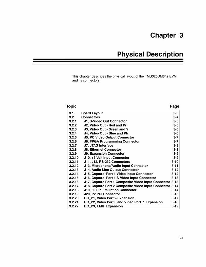
1 Introduction to the DM642 Evaluation Module . . . . . . . . . . . . . . . . . . . . . . . . . . . . . . . 1-1 Provides you with a description of the DM642 Evaluation Module, key features, and block diagram. 1.1 Key Features . . . . . . . . . . . . . . . . . . . . . . . . . . . . . . . . . . . . . . . . . . . . . . . . . . . . . . . . . . 1-2 1.2 Functional Overview . . . . . . . . . . . . . . . . . . . . . . . . . . . . . . . . . . . . . . . . . . . . . . . . . . . . 1-3 1.3 Basic Operation . . . . . . . . . . . . . . . . . . . . . . . . . . . . . . . . . . . . . . . . . . . . . . . . . . . . . . . . . 1-4 1.4 Memory Map . . . . . . . . . . . . . . . . . . . . . . . . . . . . . . . . . . . . . . . . . . . . . . . . . . . . . . . . . . 1-5 1.5 Configuration Switch Settings . . . . . . . . . . . . . . . . . . . . . . . . . . . . . . . . . . . . . . . . . . . . . 1-6 1.6 Power Supply . . . . . . . . . . . . . . . . . . . . . . . . . . . . . . . . . . . . . . . . . . . . . . . . . . . . . . . . . 1-72 Board Components . . . . . . . . . . . . . . . . . . . . . . . . . . . . . . . . . . . . . . . . . . . . . . . . . . . . . . . . 2-1 Describes the operation of the major board components on the DM642 Evaluation Module. 2.1 EMIF Interfaces . . . . . . . . . . . . . . . . . . . . . . . . . . . . . . . . . . . . . . . . . . . . . . . . . . . . . . . . . 2-2 2.1.1 SDRAM Memory Interface . . . . . . . . . . . . . . . . . . . . . . . . . . . . . . . . . . . . . . . . . . . . . . 2-2 2.1.2 Flash Memory Interface . . . . . . . . . . . . . . . . . . . . . . . . . . . . . . . . . . . . . . . . . . . . . . . . . 2-4 2.1.3 UART Interface . . . . . . . . . . . . . . . . . . . . . . . . . . . . . . . . . . . . . . . . . . . . . . . . . . 2-5 2.1.4 FPGA Asynchronous Memory Interface . . . . . . . . . . . . . . . . . . . . . . . . . . . . . . . . . . 2-5 2.1.5 FPGA Synchronous Memory Interface . . . . . . . . . . . . . . . . . . . . . . . . . . . . . . . . . . 2-6 2.1.6 EMIF Buffer/Decoder Control . . . . . . . . . . . . . . . . . . . . . . . . . . . . . . . . . . . . . . . . . 2-6 2.2 Video Port/McASP Interfaces . . . . . . . . . . . . . . . . . . . . . . . . . . . . . . . . . . . . . . . . . . . . . 2-7 2.2.1 Video Decoder Ports . . . . . . . . . . . . . . . . . . . . . . . . . . . . . . . . . . . . . . . . . . . . . . . . . . . 2-7 2.2.2 Video Encoder Ports . . . . . . . . . . . . . . . . . . . . . . . . . . . . . . . . . . . . . . . . . . . . . . . . . . . 2-7 2.2.3 FPGA Video Functions . . . . . . . . . . . . . . . . . . . . . . . . . . . . . . . . . . . . . . . . . . . . . . . . . 2-8 2.2.4 AIC23B Interface . . . . . . . . . . . . . . . . . . . . . . . . . . . . . . . . . . . . . . . . . . . . . . . . . . . . 2-9 2.2.5 Audio PLL/VCXO Circuit/PLL1708 Clock Generator . . . . . . . . . . . . . . . . . . . . . . . . . 2-10 2.3 PCI/HPI/Ethernet Interfaces . . . . . . . . . . . . . . . . . . . . . . . . . . . . . . . . . . . . . . . . . . . . . . . 2-11 2.3.1 PCI Interface . . . . . . . . . . . . . . . . . . . . . . . . . . . . . . . . . . . . . . . . . . . . . . . . . . . . . . . 2-11 2.3.2 PCI EEPROM Interface . . . . . . . . . . . . . . . . . . . . . . . . . . . . . . . . . . . . . . . . . . . . . . . . 2-11 2.3.3 Ethernet Interface . . . . . . . . . . . . . . . . . . . . . . . . . . . . . . . . . . . . . . . . . . . . . . . . . . . . 2-12 2.3.4 HPI Interface . . . . . . . . . . . . . . . . . . . . . . . . . . . . . . . . . . . . . . . . . . . . . . . . . . . . . . . . 2-12
2.4 I2C Interface . . . . . . . . . . . . . . . . . . . . . . . . . . . . . . . . . . . . . . . . . . . . . . . . . . . . . . . . . . . 2-13 2.5 SPDIF Interface . . . . . . . . . . . . . . . . . . . . . . . . . . . . . . . . . . . . . . . . . . . . . . . . . . . . . . . . 2-13 2.6 Daughter Card Interface . . . . . . . . . . . . . . . . . . . . . . . . . . . . . . . . . . . . . . . . . . . . . . . . . 2-14 2.7 Programming the FPGA . . . . . . . . . . . . . . . . . . . . . . . . . . . . . . . . . . . . . . . . . . . . . . . . . 2-15 2.8 DM642 Core CPU Clock . . . . . . . . . . . . . . . . . . . . . . . . . . . . . . . . . . . . . . . . . . . . . . . . 2-15 2.9 HDTV Implementation . . . . . . . . . . . . . . . . . . . . . . . . . . . . . . . . . . . . . . . . . . . . . . . . . . 2-16
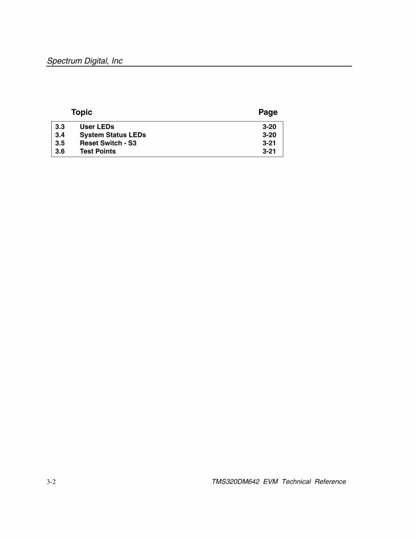
3 Physical Specifications . . . . . . . . . . . . . . . . . . . . . . . . . . . . . . . . . . . . . . . . . . . . . . . . . . . . 3-1 Describes the physical layout of the DM642 Evaluation Module and its connectors. 3.1 Board Layout . . . . . . . . . . . . . . . . . . . . . . . . . . . . . . . . . . . . . . . . . . . . . . . . . . . . . . . . 3-3 3.2 Connectors . . . . . . . . . . . . . . . . . . . . . . . . . . . . . . . . . . . . . . . . . . . . . . . . . . . . . . . . . . 3-4 3.2.1 J1, S-Video Out Connector . . . . . . . . . . . . . . . . . . . . . . . . . . . . . . . . . . . . . . . . . . 3-5 3.2.2 J2, Video Out - Red and Pr . . . . . . . . . . . . . . . . . . . . . . . . . . . . . . . . . . . . . . . . . . 3-5 3.2.3 J3, Video Out - Green and Y . . . . . . . . . . . . . . . . . . . . . . . . . . . . . . . . . . . . . . . . . 3-6 3.2.4 J4, Video Out - Blue and Pb . . . . . . . . . . . . . . . . . . . . . . . . . . . . . . . . . . . . . . . . . . 3-6 3.2.5 J5, PC Video Output Connector . . . . . . . . . . . . . . . . . . . . . . . . . . . . . . . . . . . . . . 3-7 3.2.6 J6, FPGA Programming Connector . . . . . . . . . . . . . . . . . . . . . . . . . . . . . . . . . . . 3-7 3.2.7 J7, JTAG Interface . . . . . . . . . . . . . . . . . . . . . . . . . . . . . . . . . . . . . . . . . . . . . . . . . 3-8 3.2.8 J8, Ethernet Connector . . . . . . . . . . . . . . . . . . . . . . . . . . . . . . . . . . . . . . . . . . . . . 3-8 3.2.9 J9, Expansion Connector . . . . . . . . . . . . . . . . . . . . . . . . . . . . . . . . . . . . . . . . . . . 3-9 3.2.10 J10, +5 Volt Input Connector . . . . . . . . . . . . . . . . . . . . . . . . . . . . . . . . . . . . . . . 3-9 3.2.11 J11, J12, RS-232 Connectors . . . . . . . . . . . . . . . . . . . . . . . . . . . . . . . . . . . . . . 3-10 3.2.12 J13, Microphone/Audio Input Connector . . . . . . . . . . . . . . . . . . . . . . . . . . . . . . 3-11 3.2.13 J14, Audio Line Output Connector . . . . . . . . . . . . . . . . . . . . . . . . . . . . . . . . . . 3-12 3.2.14 J15, Capture Port 1 Video Input Connector . . . . . . . . . . . . . . . . . . . . . . . . . . 3-12 3.2.15 J16, Capture Port 1 S-Video Input Connector . . . . . . . . . . . . . . . . . . . . . . . . . 3-13 3.2.16 J17, Capture Port 1 Composite Video Input Connector . . . . . . . . . . . . . . . . . 3-13 3.2.17 J18, Capture Port 2 Composite Video Input Connector . . . . . . . . . . . . . . . . . . 3-14 3.2.18 J19, 60 Pin Emulation Connector . . . . . . . . . . . . . . . . . . . . . . . . . . . . . . . . . . . 3-14 3.2.19 J20, P2 PCI Connector . . . . . . . . . . . . . . . . . . . . . . . . . . . . . . . . . . . . . . . . . . . 3-15 3.2.20 DC_P1, Video Port 2/Expansion . . . . . . . . . . . . . . . . . . . . . . . . . . . . . . . . . . 3-17 3.2.21 DC_P2, Video Port 0 and Video Port 1 Expansion . . . . . . . . . . . . . . . . . . . . . 3-18 3.2.22 DC_P3, EMIF Expansion . . . . . . . . . . . . . . . . . . . . . . . . . . . . . . . . . . . . . . . . . 3-19 3.3 User LEDs . . . . . . . . . . . . . . . . . . . . . . . . . . . . . . . . . . . . . . . . . . . . . . . . . . . . . . . . . 3-20 3.4 System Status LEDs . . . . . . . . . . . . . . . . . . . . . . . . . . . . . . . . . . . . . . . . . . . . . . . . . 3-20 3.5 Reset Switch - S3 . . . . . . . . . . . . . . . . . . . . . . . . . . . . . . . . . . . . . . . . . . . . . . . . . . . 3-21 3.6 Test Points . . . . . . . . . . . . . . . . . . . . . . . . . . . . . . . . . . . . . . . . . . . . . . . . . . . . . . . 3-21A Schematics . . . . . . . . . . . . . . . . . . . . . . . . . . . . . . . . . . . . . . . . . . . . . . . . . . . . . . . . . . . . . . A-1 Contains the schematics for the DM642 Evaluation ModuleB Mechanical Information . . . . . . . . . . . . . . . . . . . . . . . . . . . . . . . . . . . . . . . . . . . . . . . . . . B-1 Contains the mechanical information about the DM642 Evaluation Module
About This Manual
This document describes the board level operations of the TMS320DM642 EvaluationModule (EVM). The EVM is based on the Texas Instruments TMS320DM642 DigitalSignal Processor.
The DM642 Evaluation Module is a table top or PCI plug-in card that allows engineersand software developers to evaluate certain characteristics of the TMS320DM642 DSPto determine if the processor meets the designers application requirements. Evaluatorscan create software to execute on board or expand the system in a variety of ways.
Notational Conventions
This document uses the following conventions.
The DM642 Evaluation Module will sometimes be referred to as the DM642 EVM orEVM.
Program listings, program examples, and interactive displays are shown in a specialitalic typeface. Here is a sample program listing.
equations!rd = !strobe&rw;
Information About Cautions
This book may contain cautions.This is an example of a caution statement.A caution statement describes a situation that could potentially damage your software,or hardware, or other equipment. The information in a caution is provided for yourprotection. Please read each caution carefully.
Related Documents
Below are descriptions of the .pdf files. Refer to the Texas Instruments web page(http://www.ti.com) for the latest revisions of these documents.
Application Notes & User Guides
spra920.pdf: DM642 EVM Daughter card Interface Specification
sprs200b.pdf: TMS320DM642 Video/Imaging Fixed-Point Digital Signal Processor
spru041b.pdf: TMS320C6000 DSP Multichannel Audio Serial Port (McASP) Reference Guide
spru175a.pdf: TMS320C6000 DSP Inter-Integrated Circuit (I2C) Module Reference Guide
spru190d.pdf: TMS320C6000 Peripherals Reference Guide
spru295.pdf: TMS320DM642 EVM OSD FPGA User’s Guide
spru610.pdf: TMS320C64x DSP Two-Level Internal Memory Reference Guide
spru628.pdf: TMS320C6000 DSP Ethernet Media Access Controller (EMAC)/Management Data Input/Output (MDIO) Module Reference Guide
spru629.pdf: TMS320C64x DSP Video Port/VCXO Interpolated Control (VIC) Port Reference Guide
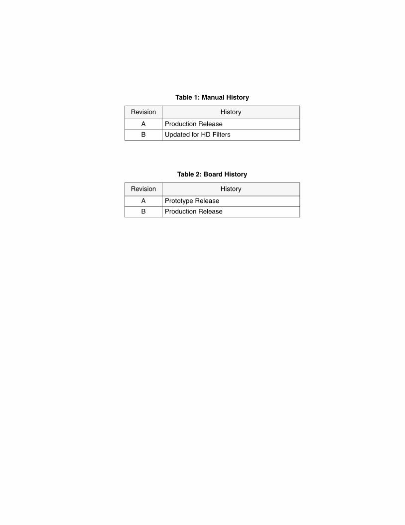
Table 1: Manual History
Revision History
A Production Release
B Updated for HD Filters
Table 2: Board History
Revision History
A Prototype Release
B Production Release

1-1
Chapter 1
Introduction to the TMS320DM642 EVM
Chapter One provides a description of the TMS320DM642 EVM alongwith the key features and a block diagram of the circuit board.
Topic Page
1.1 Key Features 1-21.2 Functional Overview 1-31.3 Basic Operation 1-41.4 Memory Map 1-51.5 Configuration Switch Settings 1-61.6 Power Supply 1-7
Spectrum Digital, Inc
1-2 TMS320DM642 EVM Technical Reference
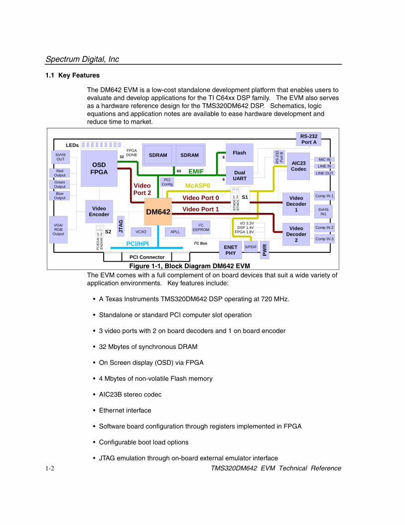
1.1 Key Features
The DM642 EVM is a low-cost standalone development platform that enables users toevaluate and develop applications for the TI C64xx DSP family. The EVM also servesas a hardware reference design for the TMS320DM642 DSP. Schematics, logicequations and application notes are available to ease hardware development andreduce time to market.
The EVM comes with a full complement of on board devices that suit a wide variety ofapplication environments. Key features include:
• A Texas Instruments TMS320DM642 DSP operating at 720 MHz.
• Standalone or standard PCI computer slot operation
• 3 video ports with 2 on board decoders and 1 on board encoder
• 32 Mbytes of synchronous DRAM
• On Screen display (OSD) via FPGA
• 4 Mbytes of non-volatile Flash memory
• AIC23B stereo codec
• Ethernet interface
• Software board configuration through registers implemented in FPGA
• Configurable boot load options
• JTAG emulation through on-board external emulator interface
Figure 1-1, Block Diagram DM642 EVMPW
R
MIC IN
LINE IN
LINE OUT
AIC23Codec
Comp IN 1
SVHSIN1
Comp IN 2
Comp IN 3
RedOutput
SVHSOUT
GreenOutput
BlueOutput
VGA/RGB
Output
OSDFPGA
VideoDecoder
1
VideoDecoder
2
VideoEncoder
SDRAM SDRAM Flash
DualUART
64 EMIF
Video Port 0
Video Port 1
VideoPort 2
McASP0
PCI Connector
I/O 3.3VDSP 1.4V
FPGA 1.8V
ENETPHY
8
8
I2CEEPROMVCXO APLL
I2C Bus
LEDsFPGADONE
JTAG
RS-232Port A
RS-
232
Port
B
PCIConfig
32
1 2
PC
IEE
AI
EN
DIA
N
S2
1 2
BTM
D0
BTM
D1
S1
PCI/HPI S/PDIF
DM642
Spectrum Digital, Inc
1-3
• 8 user LEDs
• Single voltage power supply (+5V)
• Expansion connectors for daughter card use
• Dual UART with RS-232 drivers
1.2 Functional Overview of the TMS320DM642 EVM
The DSP on the DM642 EVM interfaces to on-board peripherals through the 64-bitwide EMIF or one of the three 8/16 bit wide video ports. The SDRAM, Flash, FPGA,and UART are each connected to one of the busses. The EMIF bus is also connectedto the daughter card expansion connectors which are used for add-in boards.
On board video encoders and decoders interface to the video ports and expansionconnectors. Two decoders and one encoder are standard on the EVM. On screendisplay functions are implemented in an external FPGA which resides between theoutput video port and the video decoder.
An on-board AIC23B codec allows the DSP to transmit and receive analog audio
signals. I2C bus is used for the codec control interface and the McASP is used for data. Analog interface is done through three 3.5mm audio jacks that correspond tomicrophone input, line input, and line output. The codec can select the microphone orthe line input as the active input. The analog output is driven to the line out (fixed gain)connector. The McASP can be re-routed to the expansion connectors in software.
A programmable gate array called an FPGA is used to implement glue logic that tiesthe board components together. The FPGA also has a register based software userinterface that lets the user configure the board by reading and writing to these registers.
The EVM includes 8 LEDs which can be used to provide the user with interactivefeedback. These LEDs are accessed by reading and writing to the FPGA registers.
An included 5V external power supply is used to power the board for stand aloneapplications whereas the PC bus supplies power when used as a PCI plug in card. On-board switching voltage regulators provide the 1.4V DSP core voltage and 3.3V I/Osupplies. The board is held in reset until these supplies are within operatingspecifications. The EVM also has an LDO regulator which provides +1.8 volt FPGAcore voltage, and +3.3 volt encoder and decoder supplies.
Code Composer communicates with the EVM through an external emulator via the14 pin or 60 pin external JTAG connectors.
Spectrum Digital, Inc
1-4 TMS320DM642 EVM Technical Reference
1.3 Basic Operation
The EVM is designed to work with TI’s Code Composer Studio developmentenvironment. Code Composer communicates with the board through an external JTAGemulator. To start, follow the instructions in the Quick Start Guide to install CodeComposer. This process will install all of the necessary development tools,documentation and drivers.
Detailed information about the EVM including examples and reference material isavailable on the EVM’s CD-ROM.
Spectrum Digital, Inc
1-5
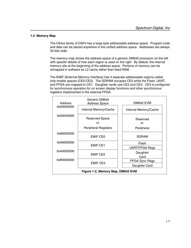
1.4 Memory Map
The C64xx family of DSPs has a large byte addressable address space. Program codeand data can be placed anywhere in the unified address space. Addresses are always32-bits wide.
The memory map shows the address space of a generic DM642 processor on the leftwith specific details of how each region is used on the right. By default, the internalmemory sits at the beginning of the address space. Portions of memory can beremapped in software as L2 cache rather than fixed RAM.
The EMIF (External Memory Interface) has 4 separate addressable regions calledchip enable spaces (CE0-CE3). The SDRAM occupies CE0 while the Flash, UART,and FPGA are mapped to CE1. Daughter cards use CE2 and CE3. CE3 is configuredfor synchronous operation for on screen display functions and other synchronousregisters implemented in the external FPGA.
Internal Memory/Cache
DM642 EVM
Reservedor
Peripheral
SDRAM
FlashUART/FPGA Regs
DaughterCard
FPGA Sync Regs
Daughter Card
Generic DM642Address SpaceAddress
0x00000000
0x00040000
0x80000000
0x90000000
0xA0000000
0xB0000000
Internal Memory/Cache
EMIF CE0
EMIF CE1
EMIF CE2
EMIF CE3
Reserved Spaceor
Peripheral Registers
Figure 1-2, Memory Map, DM642 EVM
Spectrum Digital, Inc
1-6 TMS320DM642 EVM Technical Reference
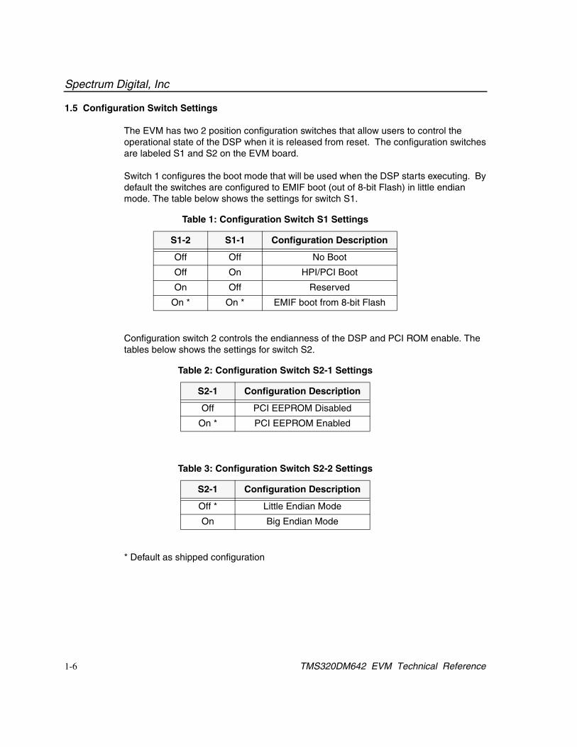
1.5 Configuration Switch Settings
The EVM has two 2 position configuration switches that allow users to control theoperational state of the DSP when it is released from reset. The configuration switchesare labeled S1 and S2 on the EVM board.
Switch 1 configures the boot mode that will be used when the DSP starts executing. Bydefault the switches are configured to EMIF boot (out of 8-bit Flash) in little endianmode. The table below shows the settings for switch S1.
Configuration switch 2 controls the endianness of the DSP and PCI ROM enable. Thetables below shows the settings for switch S2.
* Default as shipped configuration
Table 1: Configuration Switch S1 Settings
S1-2 S1-1 Configuration Description
Off Off No Boot
Off On HPI/PCI Boot
On Off Reserved
On * On * EMIF boot from 8-bit Flash
Table 2: Configuration Switch S2-1 Settings
S2-1 Configuration Description
Off PCI EEPROM Disabled
On * PCI EEPROM Enabled
Table 3: Configuration Switch S2-2 Settings
S2-1 Configuration Description
Off * Little Endian Mode
On Big Endian Mode
Spectrum Digital, Inc
1-7
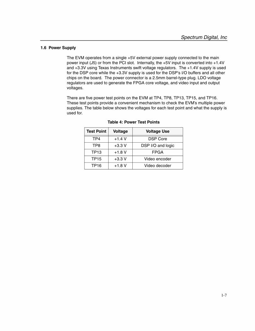
1.6 Power Supply
The EVM operates from a single +5V external power supply connected to the mainpower input (J5) or from the PCI slot. Internally, the +5V input is converted into +1.4Vand +3.3V using Texas Instruments swift voltage regulators. The +1.4V supply is usedfor the DSP core while the +3.3V supply is used for the DSP's I/O buffers and all otherchips on the board. The power connector is a 2.5mm barrel-type plug. LDO voltageregulators are used to generate the FPGA core voltage, and video input and outputvoltages.
There are five power test points on the EVM at TP4, TP8, TP13, TP15, and TP16.These test points provide a convenient mechanism to check the EVM’s multiple powersupplies. The table below shows the voltages for each test point and what the supply isused for.
Table 4: Power Test Points
Test Point Voltage Voltage Use
TP4 +1.4 V DSP Core
TP8 +3.3 V DSP I/O and logic
TP13 +1.8 V FPGA
TP15 +3.3 V Video encoder
TP16 +1.8 V Video decoder
Spectrum Digital, Inc
1-8 TMS320DM642 EVM Technical Reference
2-1
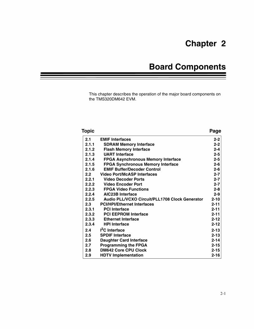
Chapter 2
Board Components
This chapter describes the operation of the major board components onthe TMS320DM642 EVM.
Topic Page
2.1 EMIF Interfaces 2-22.1.1 SDRAM Memory Interface 2-22.1.2 Flash Memory Interface 2-42.1.3 UART Interface 2-52.1.4 FPGA Asynchronous Memory Interface 2-52.1.5 FPGA Synchronous Memory Interface 2-62.1.6 EMIF Buffer/Decoder Control 2-62.2 Video Port/McASP Interfaces 2-72.2.1 Video Decoder Ports 2-72.2.2 Video Encoder Port 2-72.2.3 FPGA Video Functions 2-82.2.4 AIC23B Interface 2-92.2.5 Audio PLL/VCXO Circuit/PLL1708 Clock Generator 2-102.3 PCI/HPI/Ethernet Interfaces 2-112.3.1 PCI Interface 2-112.3.2 PCI EEPROM Interface 2-112.3.3 Ethernet Interface 2-122.3.4 HPI Interface 2-122.4 I2C Interface 2-132.5 SPDIF Interface 2-132.6 Daughter Card Interface 2-142.7 Programming the FPGA 2-152.8 DM642 Core CPU Clock 2-152.9 HDTV Implementation 2-16
Spectrum Digital, Inc
2-2 TMS320DM642 EVM Technical Reference
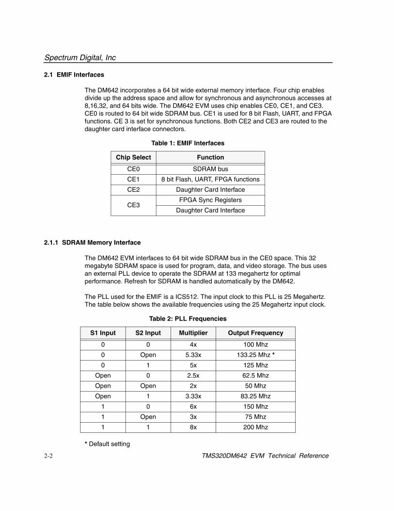
2.1 EMIF Interfaces
The DM642 incorporates a 64 bit wide external memory interface. Four chip enablesdivide up the address space and allow for synchronous and asynchronous accesses at8,16,32, and 64 bits wide. The DM642 EVM uses chip enables CE0, CE1, and CE3.CE0 is routed to 64 bit wide SDRAM bus. CE1 is used for 8 bit Flash, UART, and FPGAfunctions. CE 3 is set for synchronous functions. Both CE2 and CE3 are routed to thedaughter card interface connectors.
2.1.1 SDRAM Memory Interface
The DM642 EVM interfaces to 64 bit wide SDRAM bus in the CE0 space. This 32megabyte SDRAM space is used for program, data, and video storage. The bus usesan external PLL device to operate the SDRAM at 133 megahertz for optimalperformance. Refresh for SDRAM is handled automatically by the DM642.
The PLL used for the EMIF is a ICS512. The input clock to this PLL is 25 Megahertz.The table below shows the available frequencies using the 25 Megahertz input clock.
* Default setting
Table 1: EMIF Interfaces
Chip Select Function
CE0 SDRAM bus
CE1 8 bit Flash, UART, FPGA functions
CE2 Daughter Card Interface
CE3FPGA Sync Registers
Daughter Card Interface
Table 2: PLL Frequencies
S1 Input S2 Input Multiplier Output Frequency
0 0 4x 100 Mhz
0 Open 5.33x 133.25 Mhz *
0 1 5x 125 Mhz
Open 0 2.5x 62.5 Mhz
Open Open 2x 50 Mhz
Open 1 3.33x 83.25 Mhz
1 0 6x 150 Mhz
1 Open 3x 75 Mhz
1 1 8x 200 Mhz
Spectrum Digital, Inc
2-3
Strapping resistors R119, R121, R122, and R123 set the inputs for the S0, S1 inputs onthe PLL.
The DM642 can be configured as the source of the EMIF clock. The ECLKIN pin is thedefault on the EVM. However it is possible to operate the EMIF clock as a dividerfunction of the CPU clock. This configuration is done at reset via the ECLKINSEL0 andECLKINSEL1 pins which are shared with the EMIF address pins EA19, and EA20. Thetable below shows this configuration.
* Default
Table 3: EMIF Interfaces
ECLKINSEL0 ECLKINSEL1 Mode
0 0 ECLKIN *
0 1 CPUCLK/4
1 0 CPUCLK/6
1 1 ECLKIN
Spectrum Digital, Inc
2-4 TMS320DM642 EVM Technical Reference
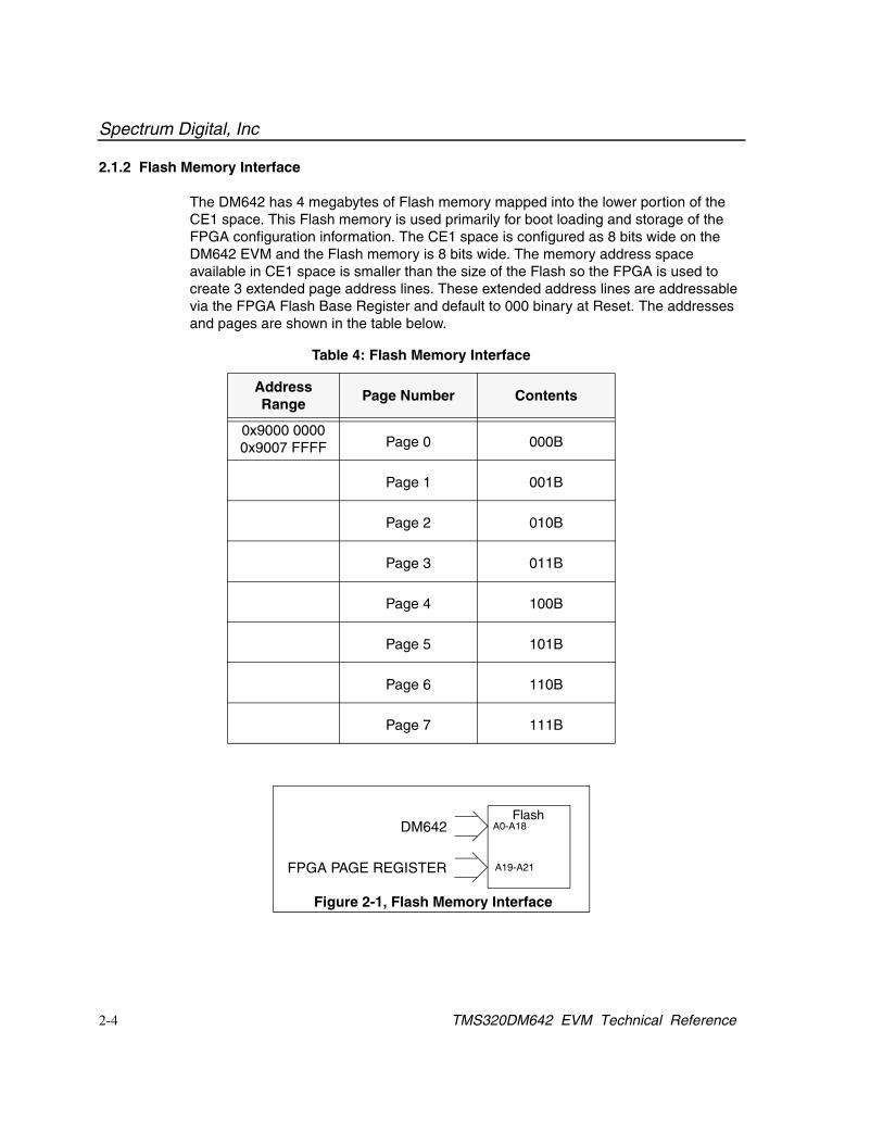
2.1.2 Flash Memory Interface
The DM642 has 4 megabytes of Flash memory mapped into the lower portion of theCE1 space. This Flash memory is used primarily for boot loading and storage of theFPGA configuration information. The CE1 space is configured as 8 bits wide on theDM642 EVM and the Flash memory is 8 bits wide. The memory address spaceavailable in CE1 space is smaller than the size of the Flash so the FPGA is used tocreate 3 extended page address lines. These extended address lines are addressablevia the FPGA Flash Base Register and default to 000 binary at Reset. The addressesand pages are shown in the table below.
Table 4: Flash Memory Interface
Address Range
Page Number Contents
0x9000 00000x9007 FFFF Page 0 000B
Page 1 001B
Page 2 010B
Page 3 011B
Page 4 100B
Page 5 101B
Page 6 110B
Page 7 111B
A0-A18
A19-A21
FlashDM642
FPGA PAGE REGISTER
Figure 2-1, Flash Memory Interface
Spectrum Digital, Inc
2-5
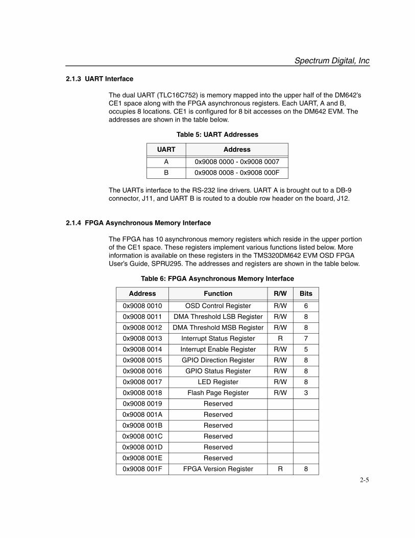
2.1.3 UART Interface
The dual UART (TLC16C752) is memory mapped into the upper half of the DM642’sCE1 space along with the FPGA asynchronous registers. Each UART, A and B,occupies 8 locations. CE1 is configured for 8 bit accesses on the DM642 EVM. Theaddresses are shown in the table below.
The UARTs interface to the RS-232 line drivers. UART A is brought out to a DB-9connector, J11, and UART B is routed to a double row header on the board, J12.
2.1.4 FPGA Asynchronous Memory Interface
The FPGA has 10 asynchronous memory registers which reside in the upper portionof the CE1 space. These registers implement various functions listed below. Moreinformation is available on these registers in the TMS320DM642 EVM OSD FPGAUser’s Guide, SPRU295. The addresses and registers are shown in the table below.
Table 5: UART Addresses
UART Address
A 0x9008 0000 - 0x9008 0007
B 0x9008 0008 - 0x9008 000F
Table 6: FPGA Asynchronous Memory Interface
Address Function R/W Bits
0x9008 0010 OSD Control Register R/W 6
0x9008 0011 DMA Threshold LSB Register R/W 8
0x9008 0012 DMA Threshold MSB Register R/W 8
0x9008 0013 Interrupt Status Register R 7
0x9008 0014 Interrupt Enable Register R/W 5
0x9008 0015 GPIO Direction Register R/W 8
0x9008 0016 GPIO Status Register R/W 8
0x9008 0017 LED Register R/W 8
0x9008 0018 Flash Page Register R/W 3
0x9008 0019 Reserved
0x9008 001A Reserved
0x9008 001B Reserved
0x9008 001C Reserved
0x9008 001D Reserved
0x9008 001E Reserved
0x9008 001F FPGA Version Register R 8
Spectrum Digital, Inc
2-6 TMS320DM642 EVM Technical Reference
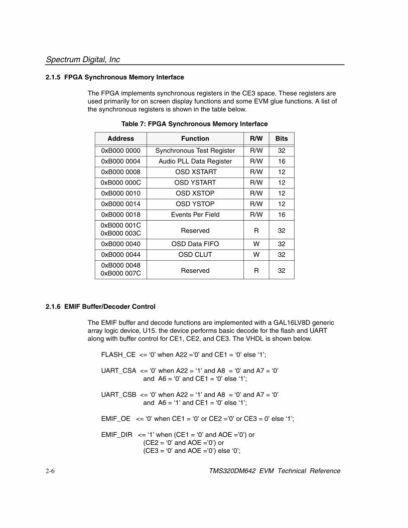
2.1.5 FPGA Synchronous Memory Interface
The FPGA implements synchronous registers in the CE3 space. These registers areused primarily for on screen display functions and some EVM glue functions. A list ofthe synchronous registers is shown in the table below.
2.1.6 EMIF Buffer/Decoder Control
The EMIF buffer and decode functions are implemented with a GAL16LV8D genericarray logic device, U15. the device performs basic decode for the flash and UARTalong with buffer control for CE1, CE2, and CE3. The VHDL is shown below.
FLASH_CE <= ‘0’ when A22 =’0’ and CE1 = ‘0’ else ‘1’;
UART_CSA <= ‘0’ when A22 = ‘1’ and A8 = ‘0’ and A7 = ‘0’and A6 = ‘0’ and CE1 = ‘0’ else ‘1’;
UART_CSB <= ‘0’ when A22 = ‘1’ and A8 = ‘0’ and A7 = ‘0’and A6 = ‘1’ and CE1 = ‘0’ else ‘1’;
EMIF_OE <= ‘0’ when CE1 = ‘0’ or CE2 =’0’ or CE3 = 0’ else ‘1’;
EMIF_DIR <= ‘1’ when (CE1 = ‘0’ and AOE =’0’) or (CE2 = ‘0’ and AOE =’0’) or (CE3 = ‘0’ and AOE =’0’) else ‘0’;
Table 7: FPGA Synchronous Memory Interface
Address Function R/W Bits
0xB000 0000 Synchronous Test Register R/W 32
0xB000 0004 Audio PLL Data Register R/W 16
0xB000 0008 OSD XSTART R/W 12
0xB000 000C OSD YSTART R/W 12
0xB000 0010 OSD XSTOP R/W 12
0xB000 0014 OSD YSTOP R/W 12
0xB000 0018 Events Per Field R/W 16
0xB000 001C0xB000 003C Reserved R 32
0xB000 0040 OSD Data FIFO W 32
0xB000 0044 OSD CLUT W 32
0xB000 00480xB000 007C Reserved R 32
Spectrum Digital, Inc
2-7
2.2 Video Port/McASP Interfaces
The DM642 has three on chip video ports. These ports can be subdivided to allowoptional functions such as an McASP or SPDIF on ports 0 and 1. The DM642 EVMuses all three of these video ports. Video Port 0 and Video Port 1 are used for captureports and Video Port 2 is used as a display port. In the standard EVM configuration, theVideo Port 0 and Video Port 1 are programmed to be subdivided to allow the McASPfunction to be implemented and interface to an TLV320AIC23B stereo Codec, or tointerface to SPDIF output J9.
2.2.1 Video Decoder Ports
On the DM642 EVM the subdivided Video Port 0 and Video Port1 are used as captureinputs, capture port 1 and capture port 2. These ports interface to TI TVP5416 andTVP5150A video decoders. The Video Ports are run through CBT switches so that theycan be selectively disabled for daughter card use. The other half of the ports are usedfor on board McASP interface. The capture port 1 interfaces to video sources via anRCA style video jack J15 and four pin S-Video mini-din connector J16. The input shouldbe a composite video source such as a DVD player or a video camera. The decoders
are programmable via the DM642’s I2C bus and can interface to all major compositevideo standards such as NTSC, PAL, and SECAM by appropriately programming theinternal registers in the decoder.
2.2.2 Video Encoder Port
The DM642’s Video Port 2 is used to drive the video encoder. It is routed through theFPGA U8 to implement advanced functions such as On Screen Display, but the defaultmode is to pass the video directly to the Phillips SAA7105 video encoder. The encodercan drive out either RGB, HD component video, NTSC/PAL composite video, or S-video depending on how the internal registers of the SAA7105 are programmed. TheSAA7105 is configured by programming the internal registers via the DM642’s I2C bus.
The encoder interfaces to composite or RGB display units. Standard Video RCA jacksprovide RGB on J2,J3, and J4. J3 the green output can also be used for interfacing tocomposite display units. An S-Video 4 pin Mini Din J1 is also available. A 15 pin HighDensity DB connector J5 allows the EVM to drive VGA type monitors.
The DM642 EVM supports High Definition TV output but requires some filter changesas specified in the section under HDTV support.
Spectrum Digital, Inc
2-8 TMS320DM642 EVM Technical Reference
2.2.3 FPGA Video Functions
The DM642 EVM uses a Xilinx XC2S300E series FPGA to implement enhanced videofunctions along with some other glue functions. In default mode the FPGA passes thevideo from the DM642’s Video Port 2 to the Phillips SAA7105 Video Encoder. ForHDTV the FPGA provides enhanced clocking and for on screen display functions theFPGA has FIFOs to mix the Video Port 2 data with the data from these internal FIFOs.The FIFO’s in the FPGA are accessed via the DM642’s EMIF in synchronous mode viathe CE3 space. For more information on the implementation of the FPGA functions, theuser should reference the document SPRU295, TMS320DM642 EVM OSD FPGAUser’s Guide.
Spectrum Digital, Inc
2-9
2.2.4 AIC23B Interface
The EVM uses a Texas Instruments AIC23B (P/N TLV320AIC23B) stereo codec forinput and output of audio signals. The codec samples analog signals on themicrophone or line inputs and converts them into digital data so it can be processed bythe DSP. When the DSP is finished with the data it uses the codec to convert thesamples back into analog signals on the line output so the user can hear the output.
The codec communicates using two serial channels, one to control the codec’s internal
configuration registers and one to send and receive digital audio samples. The I2C busis used as the unidirectional control channel. The control channel is only used whenconfiguring the codec, it is generally idle when audio data is being transmitted,
McASP is used as the bi-directional data channel. All audio data flows through thedata channel. Many data formats are supported based on the three variables ofsample width, clock signal source and serial data format. The EVM examples generallyuse a 16-bit sample width with the codec in master mode so it generates the framesync and bit clocks at the correct sample rate without effort on the DSP side. Thepreferred serial format is DSP mode which matches the McASP’s burst mode.
The codec has a programmable clock from a PLL1708 PLL device. The default systemclock is 18.432 Mhz. The internal sample rate generate subdivides the 18.432 MHzclock to generate common frequencies such as 48KHz and 8KHz. The sample rate isset by the codec’s SAMPLERATE register. The figure below shows the codec interfaceon the DM642 EVM.
Figure 2-2, TMS420DM642 EVM CODEC INTERFACE
MIC INLINE IN
LINE OUT
ADC
DAC
McASP0Data
0 LEFTINVOL1 RIGHTINVOL2 LEFTHPVOL3 RIGHTHPVOL4 ANAPATH5 DIGPATH6 POWERDOWN7 DIGIF8 SAMPLERATE9 DIGACT15 RESET
Con
trol R
egis
ters
AXR1AFSR0ACLKX0AFSX0AXR0
SCLKSDIN
I2CControlSCL0
SDA0
AIC23 Codec
Digital Analog
DOUTLRCOUT
BLKCLRCIN
DIN
I2C Format
DSP Format
LINE OUT
LINE IN
MIC IN
Spectrum Digital, Inc
2-10 TMS320DM642 EVM Technical Reference
2.2.5 Audio PLL/VCXO Circuit/PLL1708 Clock Generator
The DM642 EVM implements a multiple PLL clock generator for creating the Audioclocks for the board.
In streaming video applications the audio and video sequences can losesynchronization. The DM642 uses a VCXO interpolation circuit to incrementally speedup or slow down the STCLK input to allow for this synchronization to remain locked.
The STCLK is used to implement this feature and is created by the DM642’s VDAC pinduring a PICX100-27W Voltage Controlled Oscillator. The VDAC pin is controlled viainternal DM642 registers.
The STCLK is also a source clock for the PLL1708 programmable PLL device. Thisdevice creates the clocks for the AIC23B Codec, SPDIF, daughter card STCLK andoptional encoder clocking.
The PLL1708 is programmable via the PLL Data Register in the FPGA which serializesthe user data to the proper format required by the PLL1708.
The diagram below is a simplified diagram of this clocking scheme.
DM642
VCXOCircuit UsingPICX100-27
PLL1708
SCK03SCK02
MCK02MCK01
XT1
VDACSTCLK
PLLMS
PLLMC
PLLMD
AIC23_STCLKDM642_AHCLKX0
DC_STCLKSAA7105_STCLK
To FPGA
Figure 2-3, Audio PLL/VCXO Circuit/PLL1708 Clock Generator
STCLK
Spectrum Digital, Inc
2-11
2.3 PCI/HPI/Ethernet Interfaces
The DM642 supports a wide variety of peripheral interfaces. The DSP multiplexes aPCI bridge, host port interface, and ethernet MAC. The DM642 EVM supports all ofthese interfaces.
2.3.1 PCI Interface
The DM642 directly supports a PCI interface. Cross Bar Technology (CBT) mux andswitches are used to separate the PCI bus from the DM642 so that the EVM cansupport both the PCI interface or ethernet interface. The CBT’s also provide +5 voltinterface logic support for the PCI interface.
The CBT’s are automatically configured for PCI operation when the board is pluggedinto a PCI slot via the PCI-Detect signal
2.3.2 PCI EEPROM Interface
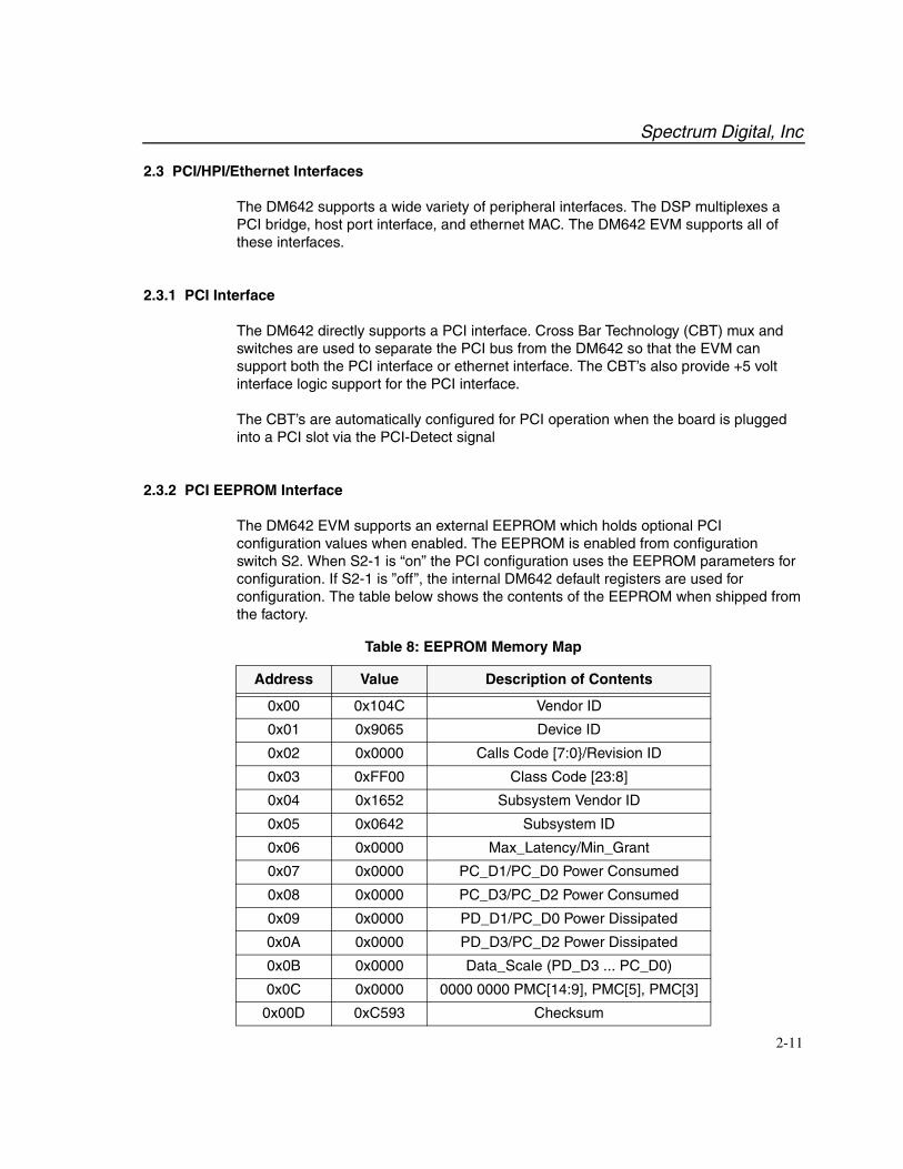
The DM642 EVM supports an external EEPROM which holds optional PCIconfiguration values when enabled. The EEPROM is enabled from configurationswitch S2. When S2-1 is “on” the PCI configuration uses the EEPROM parameters forconfiguration. If S2-1 is ”off”, the internal DM642 default registers are used forconfiguration. The table below shows the contents of the EEPROM when shipped fromthe factory.
Table 8: EEPROM Memory Map
Address Value Description of Contents
0x00 0x104C Vendor ID
0x01 0x9065 Device ID
0x02 0x0000 Calls Code [7:0}/Revision ID
0x03 0xFF00 Class Code [23:8]
0x04 0x1652 Subsystem Vendor ID
0x05 0x0642 Subsystem ID
0x06 0x0000 Max_Latency/Min_Grant
0x07 0x0000 PC_D1/PC_D0 Power Consumed
0x08 0x0000 PC_D3/PC_D2 Power Consumed
0x09 0x0000 PD_D1/PC_D0 Power Dissipated
0x0A 0x0000 PD_D3/PC_D2 Power Dissipated
0x0B 0x0000 Data_Scale (PD_D3 ... PC_D0)
0x0C 0x0000 0000 0000 PMC[14:9], PMC[5], PMC[3]
0x00D 0xC593 Checksum
Spectrum Digital, Inc
2-12 TMS320DM642 EVM Technical Reference
2.3.3 Ethernet Interface
In a standalone mode the DM642 ethernet MAC is automatically selected, and routedto the PHY via CBT muxes. The EVM DM642 uses an Intel LXT971 PHY. The10/100 Mbit interface is isolated and brought out to a RJ-45 standard ethernetconnector, J8. The PHY directly interfaces to the DM642. The ethernet address is
stored in the I2C serial ROM during manufacturing.
The RJ-45 has 2 LEDs integrated into its connector. The LEDs are green and yellowand indicate the status of the ethernet link. The green LED, when on, indicates link andwhen blinking indicates link activity. The yellow LED, when illuminated, indicates fullduplex mode.
2.3.4 HPI Interface
The DM642 is equipped with a host port that supports multiplexed or non-multiplexedaccesses. The EVM supports Host Port Interface accesses via the PCI Connector. Thesignals for the DM642’s HPI port are brought out to the PCI connectors and the usercan interface to them via these connectors. The table in Section 3 enumerates thesignals used for HPI accesses. The EVM automatically enables the EMAC when theEVM is not inserted into a PC. Furthermore, it drives the PCI_EN pin on the DM642Low disabling the PCI bus.
The HPI width signal is controlled at reset by the HD05/HWDTHSEL pin on the DM642.The default width is 16 bit mode. There is are 2 strapping resistors R206 and R207which allow the user to change the default mode for the HPI width.
When using 32 bit HPI mode the EMAC needs to be disabled, so the user will need toground B3 on the PCI forcing PCI_DETECT# low (installing R250 will also forcePCI_DETECT# low) which automatically disables the EMAC, and allows all 32 bits ofaccess to be enabled. However, to force the PCI_EN pin on the DM642 low, R249needs to be removed.
Spectrum Digital, Inc
2-13
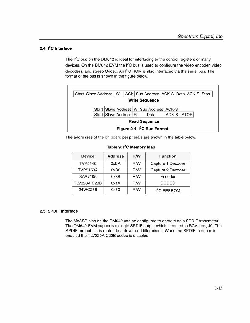
2.4 I2C Interface
The I2C bus on the DM642 is ideal for interfacing to the control registers of many
devices. On the DM642 EVM the I2C bus is used to configure the video encoder, video
decoders, and stereo Codec. An I2C ROM is also interfaced via the serial bus. Theformat of the bus is shown in the figure below.
The addresses of the on board peripherals are shown in the table below.
2.5 SPDIF Interface
The McASP pins on the DM642 can be configured to operate as a SPDIF transmitter.The DM642 EVM supports a single SPDIF output which is routed to RCA jack, J9. TheSPDIF output pin is routed to a driver and filter circuit. When the SPDIF interface isenabled the TLV320AIC23B codec is disabled.
Table 9: I2C Memory Map
Device Address R/W Function
TVP5146 0xBA R/W Capture 1 Decoder
TVP5150A 0xB8 R/W Capture 2 Decoder
SAA7105 0x88 R/W Encoder
TLV320AIC23B 0x1A R/W CODEC
24WC256 0x50 R/W I2C EEPROM
Figure 2-4, I2C Bus Format
Start Slave Address W ACK Sub Address ACK-S Data ACK-S Stop
Write Sequence
Start Slave Address W Sub Address ACK-SStart Slave Address R Data ACK-S STOP
Read Sequence
Spectrum Digital, Inc
2-14 TMS320DM642 EVM Technical Reference
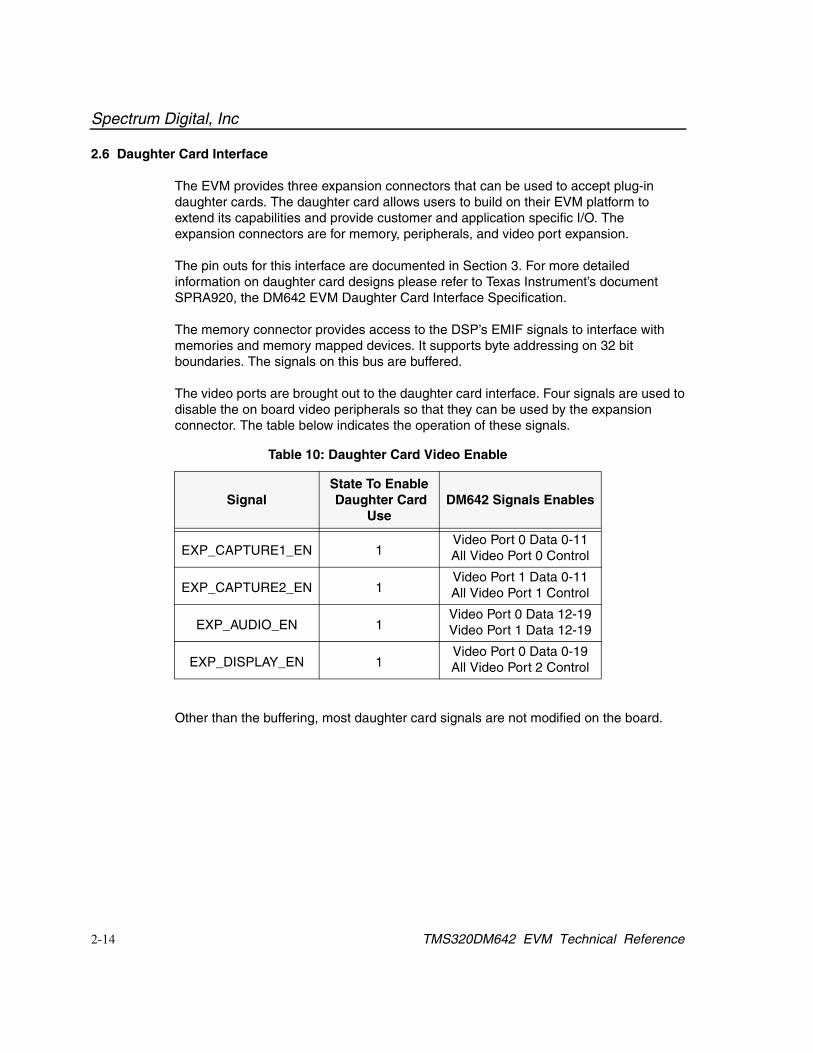
2.6 Daughter Card Interface
The EVM provides three expansion connectors that can be used to accept plug-indaughter cards. The daughter card allows users to build on their EVM platform toextend its capabilities and provide customer and application specific I/O. Theexpansion connectors are for memory, peripherals, and video port expansion.
The pin outs for this interface are documented in Section 3. For more detailedinformation on daughter card designs please refer to Texas Instrument’s documentSPRA920, the DM642 EVM Daughter Card Interface Specification.
The memory connector provides access to the DSP’s EMIF signals to interface withmemories and memory mapped devices. It supports byte addressing on 32 bitboundaries. The signals on this bus are buffered.
The video ports are brought out to the daughter card interface. Four signals are used todisable the on board video peripherals so that they can be used by the expansionconnector. The table below indicates the operation of these signals.
Other than the buffering, most daughter card signals are not modified on the board.
Table 10: Daughter Card Video Enable
SignalState To Enable Daughter Card
UseDM642 Signals Enables
EXP_CAPTURE1_EN 1Video Port 0 Data 0-11All Video Port 0 Control
EXP_CAPTURE2_EN 1Video Port 1 Data 0-11All Video Port 1 Control
EXP_AUDIO_EN 1Video Port 0 Data 12-19Video Port 1 Data 12-19
EXP_DISPLAY_EN 1Video Port 0 Data 0-19All Video Port 2 Control
Spectrum Digital, Inc
2-15
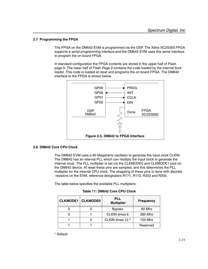
2.7 Programming the FPGA
The FPGA on the DM642 EVM is programmed via the DSP. The Xilinx XC2S300 FPGAsupports a serial programming interface and the DM642 EVM uses this serial interfaceto program the on board FPGA.
In standard configuration the FPGA contents are stored in the upper half of Flashpage 0. The lower half of Flash Page 0 contains the code loaded by the internal bootloader. This code is loaded at reset and programs the on board FPGA. The DM642interface to the FPGA is shown below.
2.8 DM642 Core CPU Clock
The DM642 EVM uses a 60 Megahertz oscillator to generate the input clock CLKIN.The DM642 has an internal PLL which can multiply the input clock to generate theinternal clock. The PLL multiplier is set via the CLKMODE0 and CLKMODE1 pins onthe DM642 device. At reset these pins are sampled, and this determines the PLLmultiplier for the internal CPU clock. The strapping of these pins is done with discrete resistors on the EVM, reference designators R171, R172, R203 and R205.
The table below specifies the available PLL multipliers.
* Default
Table 11: DM642 Core CPU Clock
CLKMODE1 CLKMODE0PLL
MultiplierFrequency
0 0 Bypass 60 Mhz
0 1 CLKIN times 6 360 Mhz
1 0 CLKIN times 12 * 720 Mhz
1 1 Reserved
PROGINITCCLK
DIN
GP00GP06GP01
GP02
DSPDM642
Done FPGAXC2S300E
Figure 2-5, DM642 to FPGA Interface
Spectrum Digital, Inc
2-16 TMS320DM642 EVM Technical Reference
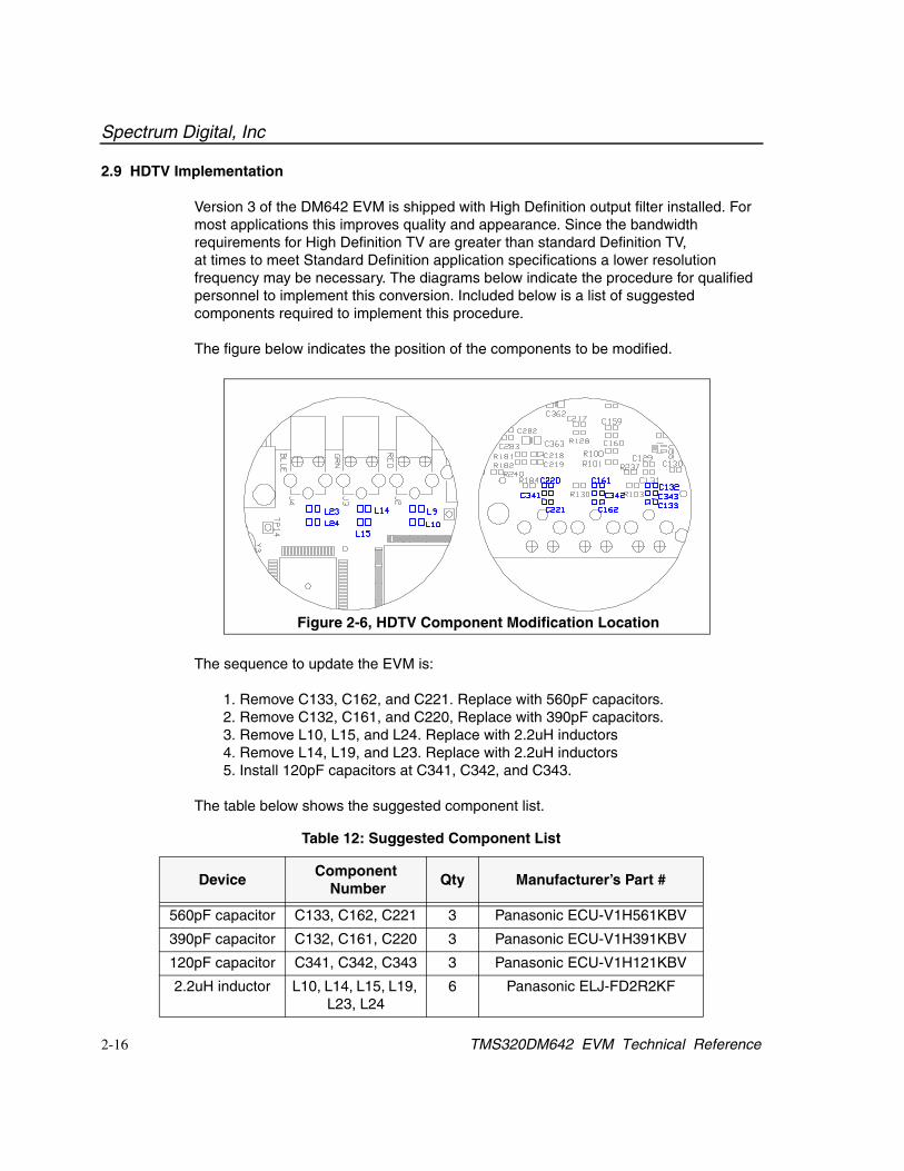
2.9 HDTV Implementation
Version 3 of the DM642 EVM is shipped with High Definition output filter installed. Formost applications this improves quality and appearance. Since the bandwidthrequirements for High Definition TV are greater than standard Definition TV,at times to meet Standard Definition application specifications a lower resolutionfrequency may be necessary. The diagrams below indicate the procedure for qualifiedpersonnel to implement this conversion. Included below is a list of suggestedcomponents required to implement this procedure.
The figure below indicates the position of the components to be modified.
The sequence to update the EVM is:
1. Remove C133, C162, and C221. Replace with 560pF capacitors.2. Remove C132, C161, and C220, Replace with 390pF capacitors.3. Remove L10, L15, and L24. Replace with 2.2uH inductors4. Remove L14, L19, and L23. Replace with 2.2uH inductors5. Install 120pF capacitors at C341, C342, and C343.
The table below shows the suggested component list.
Table 12: Suggested Component List
DeviceComponent
NumberQty Manufacturer’s Part #
560pF capacitor C133, C162, C221 3 Panasonic ECU-V1H561KBV
390pF capacitor C132, C161, C220 3 Panasonic ECU-V1H391KBV
120pF capacitor C341, C342, C343 3 Panasonic ECU-V1H121KBV
2.2uH inductor L10, L14, L15, L19, L23, L24
6 Panasonic ELJ-FD2R2KF
Figure 2-6, HDTV Component Modification Location
Spectrum Digital, Inc
2-17
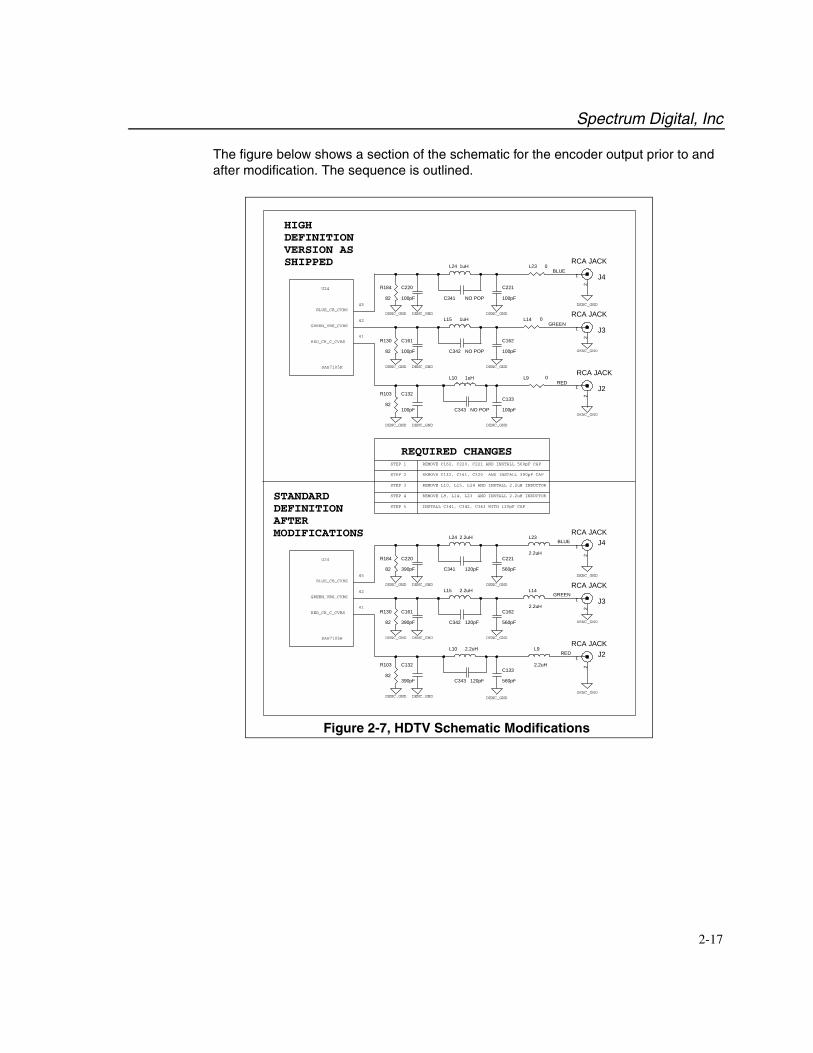
The figure below shows a section of the schematic for the encoder output prior to andafter modification. The sequence is outlined.
Figure 2-7, HDTV Schematic Modifications
DENC_GND
DENC_GND
DENC_GND DENC_GNDDENC_GND
DENC_GND
DENC_GND
DENC_GND
DENC_GND
DENC_GND
DENC_GND
DENC_GND
DENC_GND
SAA7105H
U24
45
42
41RED_CR_C_CVBS
GREEN_VBS_CVBS
BLUE_CB_CVBS
HIGHDEFINITIONVERSION ASSHIPPED
REMOVE L9, L14, L23 AND INSTALL 2.2uH INDUCTOR
REMOVE L10, L15, L24 AND INSTALL 2.2uH INDUCTOR
REMOVE C132, C161, C220 AND INSTALL 390pF CAP
REMOVE C162, C220, C221 AND INSTALL 560pF CAP
INSTALL C341, C342, C343 WITH 120pF CAP
STEP 1
STEP 2
STEP 3
STEP 4
STEP 5
REQUIRED CHANGES
DENC_GND
DENC_GND
DENC_GND DENC_GND
DENC_GND
DENC_GND
DENC_GND
DENC_GND
DENC_GNDDENC_GND
DENC_GND
SAA7105H
U24
45
42
41RED_CR_C_CVBS
GREEN_VBS_CVBS
BLUE_CB_CVBS
STANDARDDEFINITIONAFTERMODIFICATIONS
GREEN
RED
BLUE
BLUE
RED
GREEN
J4
RCA JACK
1
2
C343 NO POP
L10 1uH
C133
100pF
C220
100pF
R184
82
C132
100pF
R130
82 C342 NO POP
C162
100pF
L15 1uH
L24 1uH
R103
82
J2
RCA JACK
1
2
C341 NO POP
J3
RCA JACK
1
2
C161
100pF
C221
100pF
C133
560pF
C132
390pF
C341 120pF
R103
82
J2RCA JACK
1
2
J3
RCA JACK
1
2
C342 120pF
C162
560pF
C161
390pF
R184
82
L24 2.2uH
L15 2.2uH
L10 2.2uH
J4RCA JACK
1
2
R130
82
L9
2.2uH
L14
2.2uH
L23
2.2uHC221
560pF
C220
390pF
C343 120pF
L9
0
L14
0
L23 0
Spectrum Digital, Inc
2-18 TMS320DM642 EVM Technical Reference
3-1
Chapter 3
Physical Description
This chapter describes the physical layout of the TMS320DM642 EVMand its connectors.
Topic Page
3.1 Board Layout 3-33.2 Connectors 3-43.2.1 J1, S-Video Out Connector 3-53.2.2 J2, Video Out - Red and Pr 3-53.2.3 J3, Video Out - Green and Y 3-63.2.4 J4, Video Out - Blue and Pb 3-63.2.5 J5, PC Video Output Connector 3-73.2.6 J6, FPGA Programming Connector 3-73.2.7 J7, JTAG Interface 3-83.2.8 J8, Ethernet Connector 3-83.2.9 J9, Expansion Connector 3-93.2.10 J10, +5 Volt Input Connector 3-93.2.11 J11, J12, RS-232 Connectors 3-103.2.12 J13, Microphone/Audio Input Connector 3-113.2.13 J14, Audio Line Output Connector 3-123.2.14 J15, Capture Port 1 Video Input Connector 3-123.2.15 J16, Capture Port 1 S-Video Input Connector 3-133.2.16 J17, Capture Port 1 Composite Video Input Connector 3-133.2.17 J18, Capture Port 2 Composite Video Input Connector 3-143.2.18 J19, 60 Pin Emulation Connector 3-143.2.19 J20, P2 PCI Connector 3-153.2.20 DC_P1, Video Port 2/Expansion 3-173.2.21 DC_P2, Video Port 0 and Video Port 1 Expansion 3-183.2.22 DC_P3, EMIF Expansion 3-19
Spectrum Digital, Inc
3-2 TMS320DM642 EVM Technical Reference
Topic Page
3.3 User LEDs 3-203.4 System Status LEDs 3-203.5 Reset Switch - S3 3-213.6 Test Points 3-21
Spectrum Digital, Inc
3-3
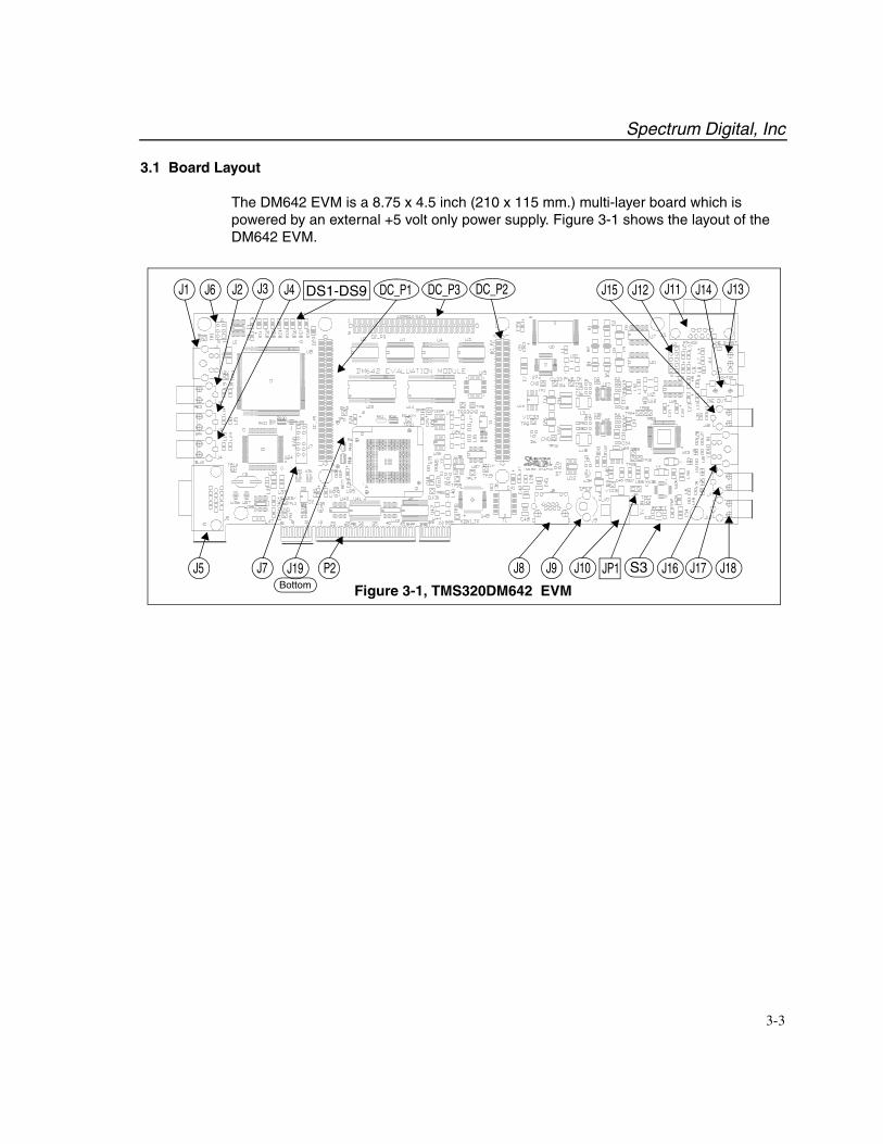
3.1 Board Layout
The DM642 EVM is a 8.75 x 4.5 inch (210 x 115 mm.) multi-layer board which ispowered by an external +5 volt only power supply. Figure 3-1 shows the layout of the DM642 EVM.
Figure 3-1, TMS320DM642 EVM
S3J5 J7 P2 J8 J9
J12J4J3J2J1 J11 J13
J10
J6 DC_P1DS1-DS9 DC_P2DC_P3
J17
J15
J16 J18J19Bottom
J14
JP1
Spectrum Digital, Inc
3-4 TMS320DM642 EVM Technical Reference
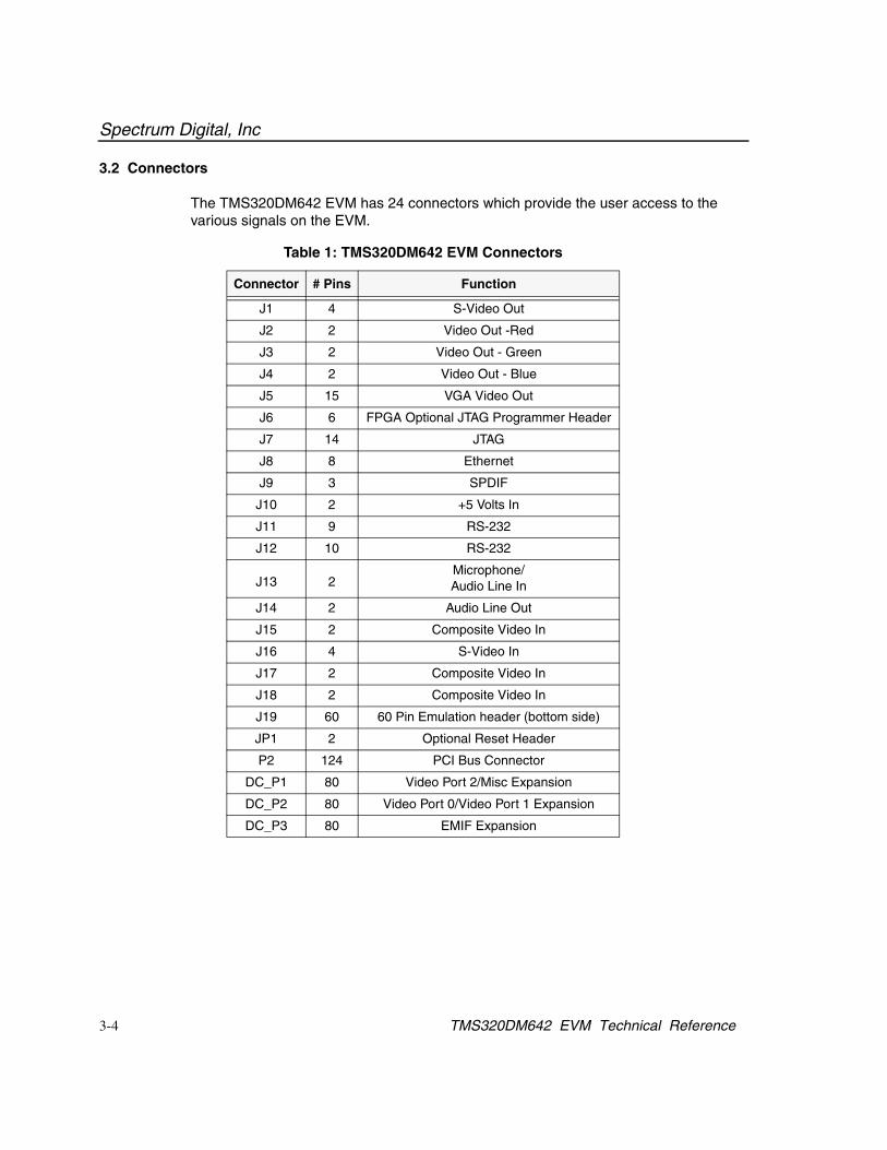
3.2 Connectors
The TMS320DM642 EVM has 24 connectors which provide the user access to thevarious signals on the EVM.
Table 1: TMS320DM642 EVM Connectors
Connector # Pins Function
J1 4 S-Video Out
J2 2 Video Out -Red
J3 2 Video Out - Green
J4 2 Video Out - Blue
J5 15 VGA Video Out
J6 6 FPGA Optional JTAG Programmer Header
J7 14 JTAG
J8 8 Ethernet
J9 3 SPDIF
J10 2 +5 Volts In
J11 9 RS-232
J12 10 RS-232
J13 2Microphone/Audio Line In
J14 2 Audio Line Out
J15 2 Composite Video In
J16 4 S-Video In
J17 2 Composite Video In
J18 2 Composite Video In
J19 60 60 Pin Emulation header (bottom side)
JP1 2 Optional Reset Header
P2 124 PCI Bus Connector
DC_P1 80 Video Port 2/Misc Expansion
DC_P2 80 Video Port 0/Video Port 1 Expansion
DC_P3 80 EMIF Expansion
Spectrum Digital, Inc
3-5
3.2.1 J1, S-Video Out Connector
J1 is a four pin mini din connector which interfaces to an output display device. Theconnector is driven directly by the Philips SAA7105 video encoder. The pin out is theconnector is shown below.
3.2.2 J2, Video Out - RED and Pr
J2 is a RCA jack which drives the RED signal when the encoder is in the R-G-B mode.This output is also used in HDTV mode to drive the Pr component of the video. Thepinout of this connector is shown below.
Table 2: J1, Mini Din Connector
Pin # Signal Name
1 Ground
2 Ground
3 Luma (Y)
4 Chroma (C)
Pin 1 Pin 2Pin 3 Pin 4
Figure 3-2, Front View, Mini Din Connector
Figure 3-3, J2, RCA Jack
Shield (ground)
Signal Output
Spectrum Digital, Inc
3-6 TMS320DM642 EVM Technical Reference
3.2.3 J3, Video Out - Green and Y
J3 is an RCA jack used to interface to the GREEN or composite video of the displaydevice. This connector is driven directly by the Philips SAA7105 video encoder. Thisoutput is also used in HDTV mode to drive the Y component of the video. The pinout ofthis connector is shown below.
3.2.4 J4, Video Out - Blue and Pb
J4 is an RCA jack used to interface to the Blue of an RGB device. This connector isdriven directly by the Philips SAA7105 video encoder. This output is also used in HDTVmode to drive the Pb component of the video. The pinout of this connector is shownbelow.
Figure 3-4, J3, RCA Jack
Shield (ground)
Signal Output
Figure 3-5, J4, RCA Jack
Shield (ground)
Signal Output
Spectrum Digital, Inc
3-7
3.2.5 J5, PC Video Output Connector
Connector J5 provides the standard personal computer monitor video output 15 pinhigh density female D-connector. The signals on the pins are shown in the table below.
3.2.6 J6, FPGA Programming Connector
Connector J6 is 2 x 3 double row header allowing JTAG programming the FPGA, U8.The signals on the pins are shown in the table below. This interfaces to a Xilinxprogramming pod.
Table 3: J5, PC Video Output Connector
Pin # Signal Name
1 Red
2 Green
3 Blue
4 No connect
5 Ground
6 Ground
7 Ground
8 Ground
9 Key
10 Ground
11 No connect
12 No connect
13 Horizontal Sync
14 Vertical sync
15 No Connect
Table 4: J6, FPGA Programming Connector
Pin # Signal Name
1 +3.3 Volts
2 Ground
3 FPGA-TCK
4 FPGA-TDI
5 FPGA-TDO
6 FPGA-TMS
Spectrum Digital, Inc
3-8 TMS320DM642 EVM Technical Reference
3.2.7 J7, JTAG Interface
The TMS320DM642 EVM is supplied with a 14 pin header interface, J7. This is thestandard interface used by JTAG emulators to interface to Texas Instruments DSPs.The pinout for the connector is shown in the figure below.
3.2.8 J8, Ethernet Connector
Connector J8 is a standard RJ-45 ethernet connector. The connector pin out is shown
Table 5: J8 Connector Pin Out
Pin # Signal Name
1 LXT TXD
2 LXT TXM
3 LXT RXP
4 Terminator 1
5 Terminator 2
6 LXT RXM
7 Terminator 3
8 Terminator 4
1 23 4
5 67 89 1011 1213 14
TMSTDI
PD (+3.3V)TDO
TCK-RET
TCKEMU0
TRST-GNDno pin (key)GNDGND
GNDEMU1
Header Dimensions
Pin-to-Pin spacing, 0.100 in. (X,Y)Pin width, 0.025-in. square post
Pin length, 0.235-in. nominal
Figure 3-6, JTAG INTERFACE
Spectrum Digital, Inc
3-9
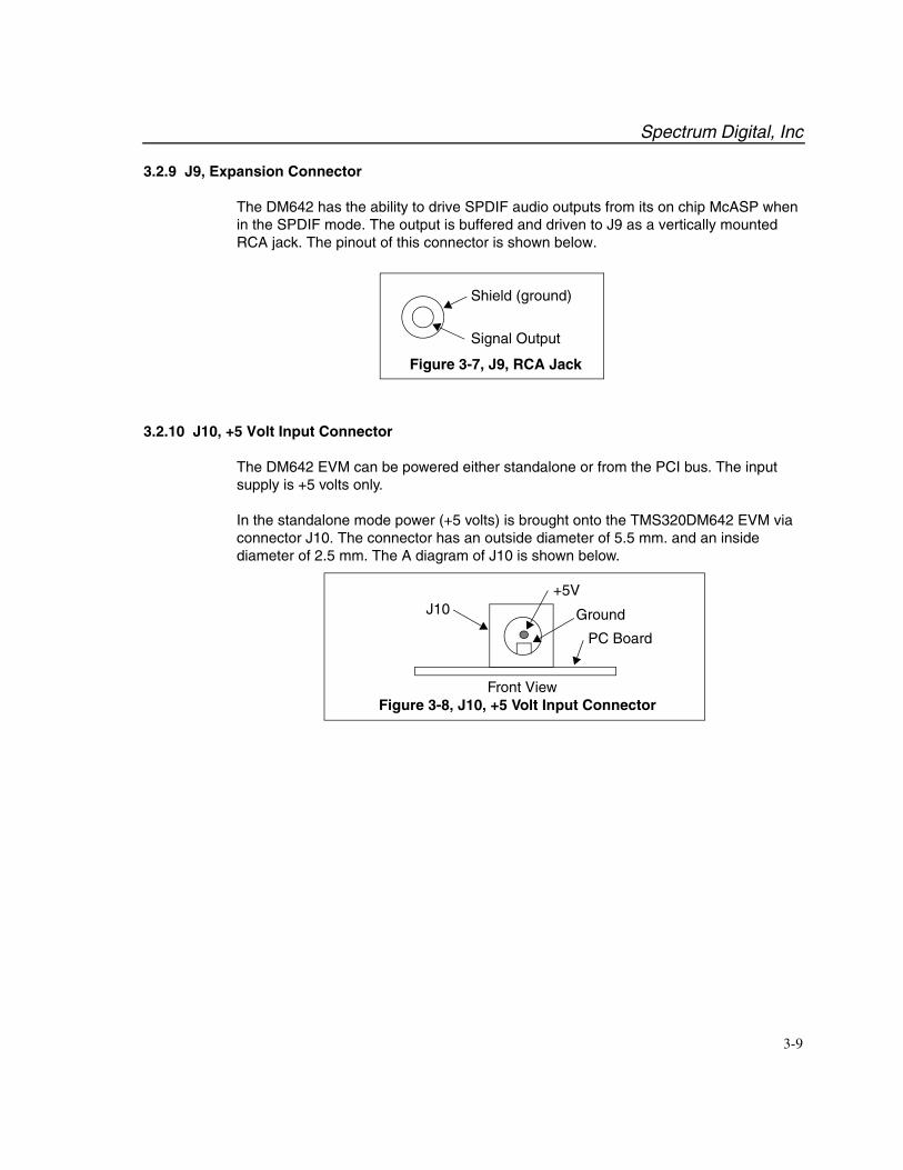
3.2.9 J9, Expansion Connector
The DM642 has the ability to drive SPDIF audio outputs from its on chip McASP whenin the SPDIF mode. The output is buffered and driven to J9 as a vertically mountedRCA jack. The pinout of this connector is shown below.
3.2.10 J10, +5 Volt Input Connector
The DM642 EVM can be powered either standalone or from the PCI bus. The inputsupply is +5 volts only.
In the standalone mode power (+5 volts) is brought onto the TMS320DM642 EVM viaconnector J10. The connector has an outside diameter of 5.5 mm. and an insidediameter of 2.5 mm. The A diagram of J10 is shown below.
Figure 3-7, J9, RCA Jack
Shield (ground)
Signal Output
PC Board
J10+5V
Ground
Front ViewFigure 3-8, J10, +5 Volt Input Connector
Spectrum Digital, Inc
3-10 TMS320DM642 EVM Technical Reference
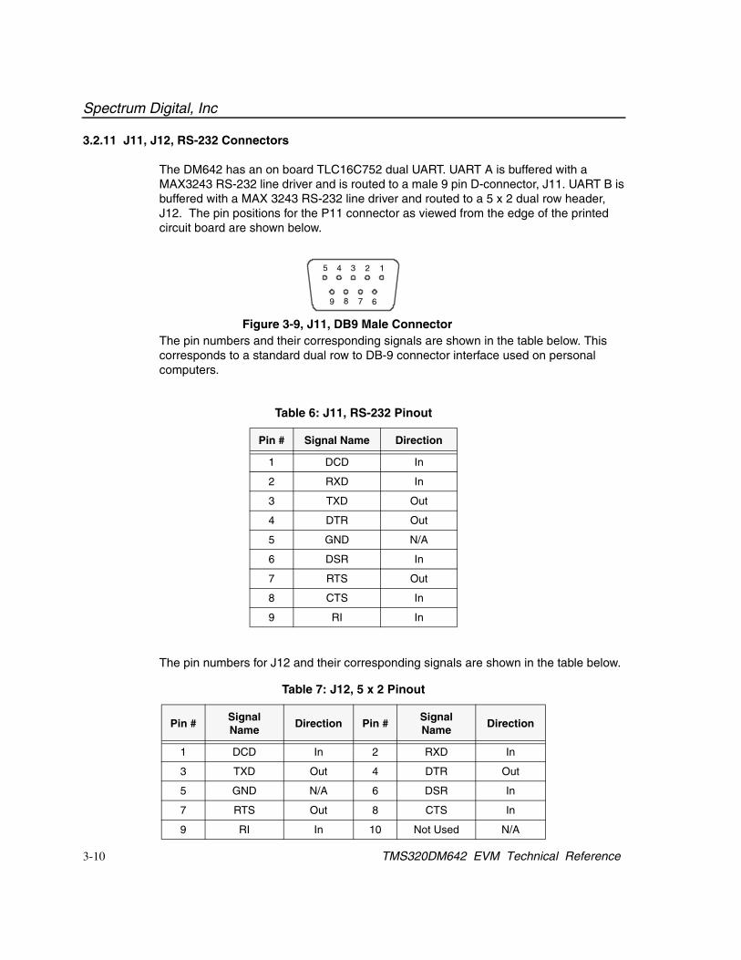
3.2.11 J11, J12, RS-232 Connectors
The DM642 has an on board TLC16C752 dual UART. UART A is buffered with aMAX3243 RS-232 line driver and is routed to a male 9 pin D-connector, J11. UART B isbuffered with a MAX 3243 RS-232 line driver and routed to a 5 x 2 dual row header,J12. The pin positions for the P11 connector as viewed from the edge of the printedcircuit board are shown below.
The pin numbers and their corresponding signals are shown in the table below. Thiscorresponds to a standard dual row to DB-9 connector interface used on personalcomputers.
The pin numbers for J12 and their corresponding signals are shown in the table below.
Table 6: J11, RS-232 Pinout
Pin # Signal Name Direction
1 DCD In
2 RXD In
3 TXD Out
4 DTR Out
5 GND N/A
6 DSR In
7 RTS Out
8 CTS In
9 RI In
Table 7: J12, 5 x 2 Pinout
Pin #Signal Name
Direction Pin #Signal Name
Direction
1 DCD In 2 RXD In
3 TXD Out 4 DTR Out
5 GND N/A 6 DSR In
7 RTS Out 8 CTS In
9 RI In 10 Not Used N/A
9
5 4 3 2 1
8 7 6
Figure 3-9, J11, DB9 Male Connector
Spectrum Digital, Inc
3-11
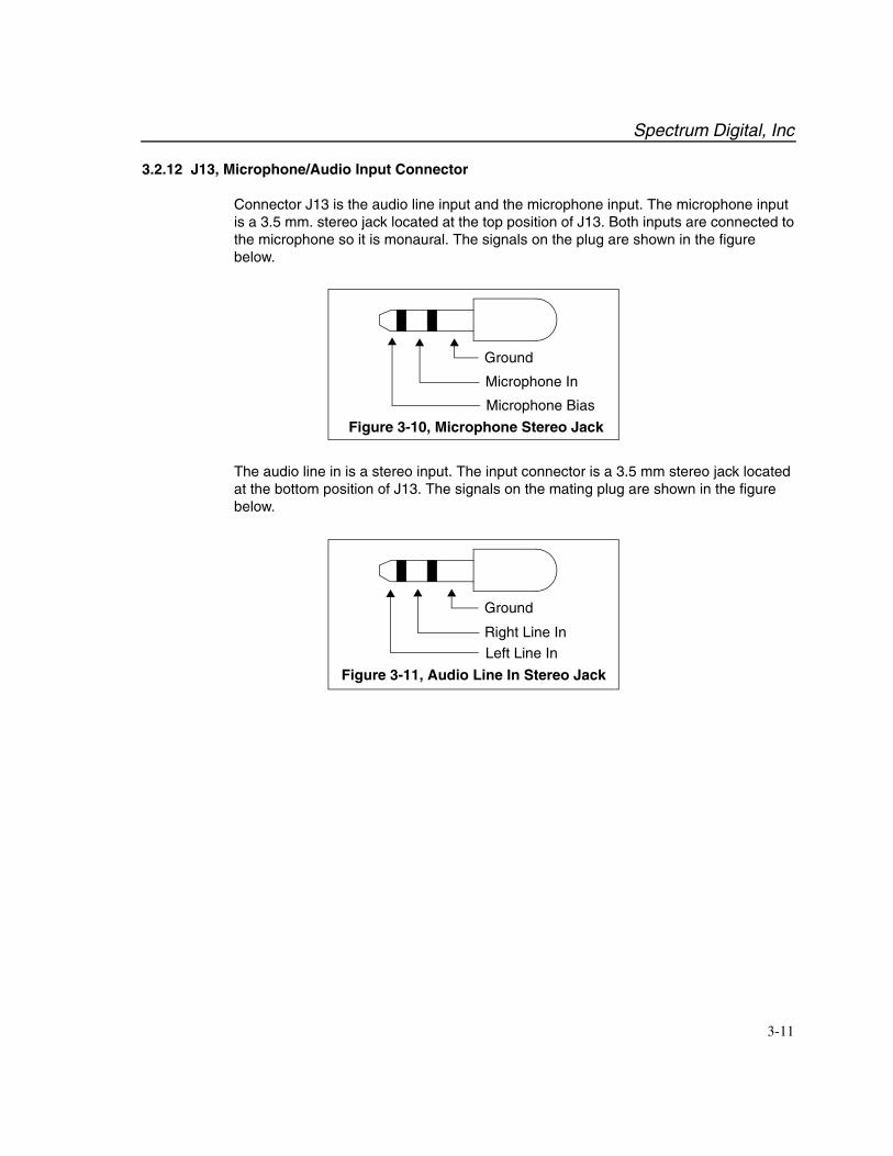
3.2.12 J13, Microphone/Audio Input Connector
Connector J13 is the audio line input and the microphone input. The microphone inputis a 3.5 mm. stereo jack located at the top position of J13. Both inputs are connected tothe microphone so it is monaural. The signals on the plug are shown in the figurebelow.
The audio line in is a stereo input. The input connector is a 3.5 mm stereo jack locatedat the bottom position of J13. The signals on the mating plug are shown in the figurebelow.
Microphone In
Ground
Figure 3-10, Microphone Stereo Jack
Microphone Bias
Left Line In
Ground
Figure 3-11, Audio Line In Stereo Jack
Right Line In
Spectrum Digital, Inc
3-12 TMS320DM642 EVM Technical Reference
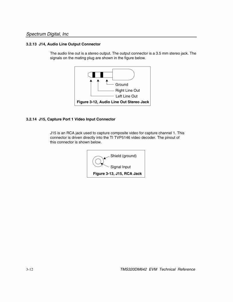
3.2.13 J14, Audio Line Output Connector
The audio line out is a stereo output. The output connector is a 3.5 mm stereo jack. Thesignals on the mating plug are shown in the figure below.
3.2.14 J15, Capture Port 1 Video Input Connector
J15 is an RCA jack used to capture composite video for capture channel 1. Thisconnector is driven directly into the TI TVP5146 video decoder. The pinout ofthis connector is shown below.
Left Line Out
Ground
Figure 3-12, Audio Line Out Stereo Jack
Right Line Out
Figure 3-13, J15, RCA Jack
Shield (ground)
Signal Input
Spectrum Digital, Inc
3-13
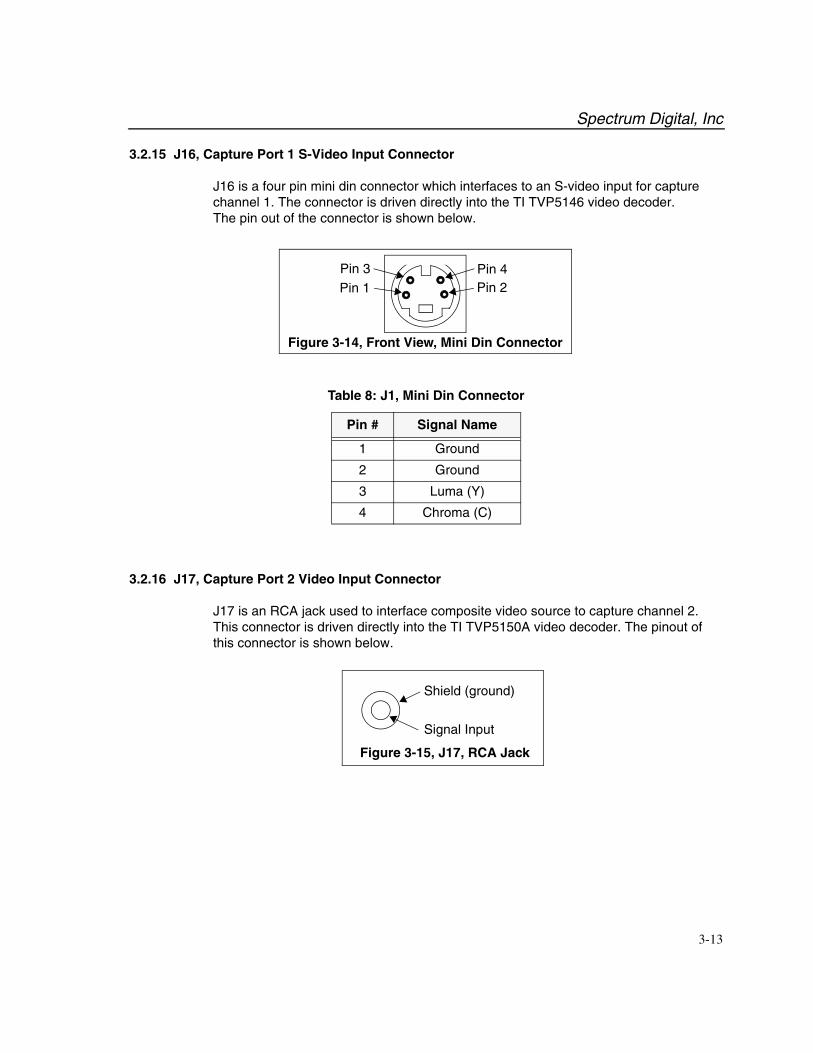
3.2.15 J16, Capture Port 1 S-Video Input Connector
J16 is a four pin mini din connector which interfaces to an S-video input for capturechannel 1. The connector is driven directly into the TI TVP5146 video decoder.The pin out of the connector is shown below.
3.2.16 J17, Capture Port 2 Video Input Connector
J17 is an RCA jack used to interface composite video source to capture channel 2.This connector is driven directly into the TI TVP5150A video decoder. The pinout ofthis connector is shown below.
Table 8: J1, Mini Din Connector
Pin # Signal Name
1 Ground
2 Ground
3 Luma (Y)
4 Chroma (C)
Pin 1 Pin 2Pin 3 Pin 4
Figure 3-14, Front View, Mini Din Connector
Figure 3-15, J17, RCA Jack
Shield (ground)
Signal Input
Spectrum Digital, Inc
3-14 TMS320DM642 EVM Technical Reference
3.2.17 J18, Capture Port 2 Optional Video Input Connector
J18 is an RCA jack used to interface composite video source to capture channel 2.This connector is driven directly into the TI TVP5150A video decoder. The pinout ofthis connector is shown below.
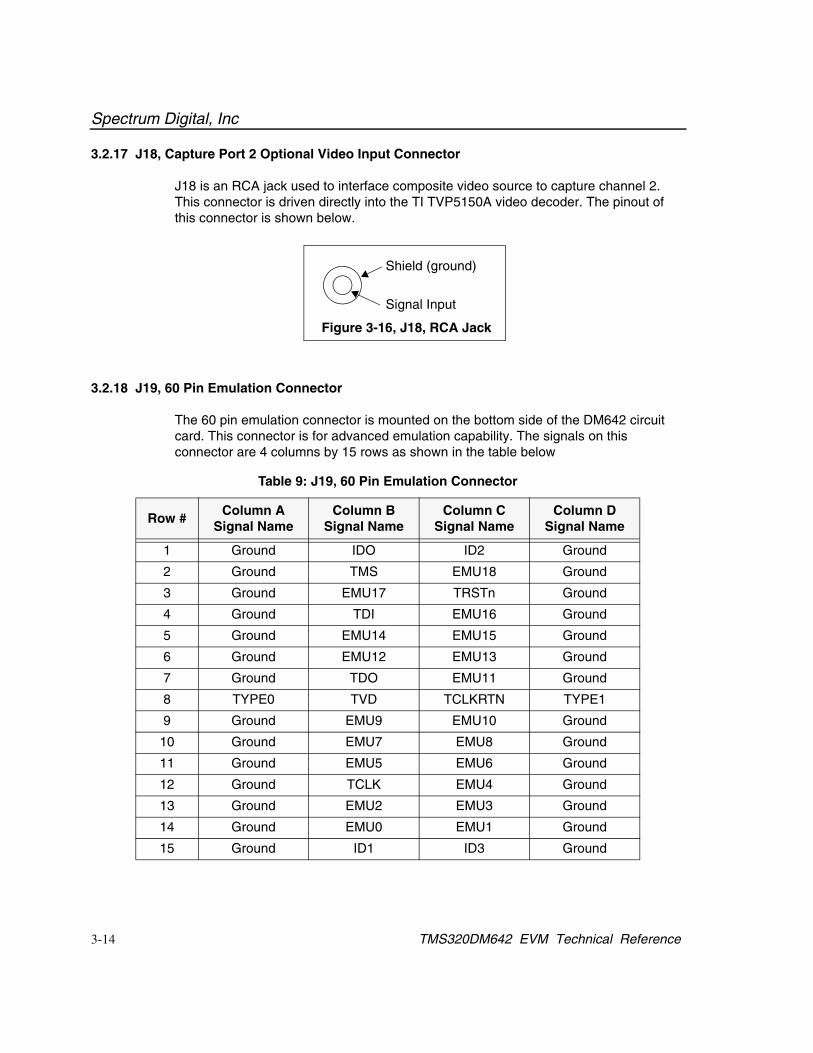
3.2.18 J19, 60 Pin Emulation Connector
The 60 pin emulation connector is mounted on the bottom side of the DM642 circuitcard. This connector is for advanced emulation capability. The signals on thisconnector are 4 columns by 15 rows as shown in the table below
Table 9: J19, 60 Pin Emulation Connector
Row #Column A
Signal NameColumn B
Signal NameColumn C
Signal NameColumn D
Signal Name
1 Ground IDO ID2 Ground
2 Ground TMS EMU18 Ground
3 Ground EMU17 TRSTn Ground
4 Ground TDI EMU16 Ground
5 Ground EMU14 EMU15 Ground
6 Ground EMU12 EMU13 Ground
7 Ground TDO EMU11 Ground
8 TYPE0 TVD TCLKRTN TYPE1
9 Ground EMU9 EMU10 Ground
10 Ground EMU7 EMU8 Ground
11 Ground EMU5 EMU6 Ground
12 Ground TCLK EMU4 Ground
13 Ground EMU2 EMU3 Ground
14 Ground EMU0 EMU1 Ground
15 Ground ID1 ID3 Ground
Figure 3-16, J18, RCA Jack
Shield (ground)
Signal Input
Spectrum Digital, Inc
3-15
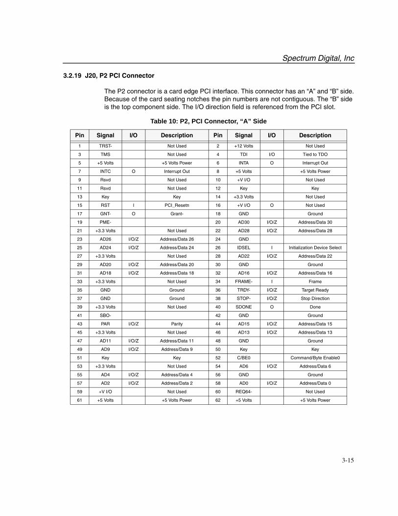
3.2.19 J20, P2 PCI Connector
The P2 connector is a card edge PCI interface. This connector has an “A” and “B” side.Because of the card seating notches the pin numbers are not contiguous. The “B” sideis the top component side. The I/O direction field is referenced from the PCI slot.
Table 10: P2, PCI Connector, “A” Side
Pin Signal I/O Description Pin Signal I/O Description
1 TRST- Not Used 2 +12 Volts Not Used
3 TMS Not Used 4 TDI I/O Tied to TDO
5 +5 Volts +5 Volts Power 6 INTA O Interrupt Out
7 INTC O Interrupt Out 8 +5 Volts +5 Volts Power
9 Rsvd Not Used 10 +V I/O Not Used
11 Rsvd Not Used 12 Key Key
13 Key Key 14 +3.3 Volts Not Used
15 RST I PCI_Resetn 16 +V I/O O Not Used
17 GNT- O Grant- 18 GND Ground
19 PME- 20 AD30 I/O/Z Address/Data 30
21 +3.3 Volts Not Used 22 AD28 I/O/Z Address/Data 28
23 AD26 I/O/Z Address/Data 26 24 GND
25 AD24 I/O/Z Address/Data 24 26 IDSEL I Initialization Device Select
27 +3.3 Volts Not Used 28 AD22 I/O/Z Address/Data 22
29 AD20 I/O/Z Address/Data 20 30 GND Ground
31 AD18 I/O/Z Address/Data 18 32 AD16 I/O/Z Address/Data 16
33 +3.3 Volts Not Used 34 FRAME- I Frame
35 GND Ground 36 TRDY- I/O/Z Target Ready
37 GND Ground 38 STOP- I/O/Z Stop Direction
39 +3.3 Volts Not Used 40 SDONE O Done
41 SBO- 42 GND Ground
43 PAR I/O/Z Parity 44 AD15 I/O/Z Address/Data 15
45 +3.3 Volts Not Used 46 AD13 I/O/Z Address/Data 13
47 AD11 I/O/Z Address/Data 11 48 GND Ground
49 AD9 I/O/Z Address/Data 9 50 Key Key
51 Key Key 52 C/BE0 Command/Byte Enable0
53 +3.3 Volts Not Used 54 AD6 I/O/Z Address/Data 6
55 AD4 I/O/Z Address/Data 4 56 GND Ground
57 AD2 I/O/Z Address/Data 2 58 AD0 I/O/Z Address/Data 0
59 +V I/O Not Used 60 REQ64- Not Used
61 +5 Volts +5 Volts Power 62 +5 Volts +5 Volts Power
Spectrum Digital, Inc
3-16 TMS320DM642 EVM Technical Reference
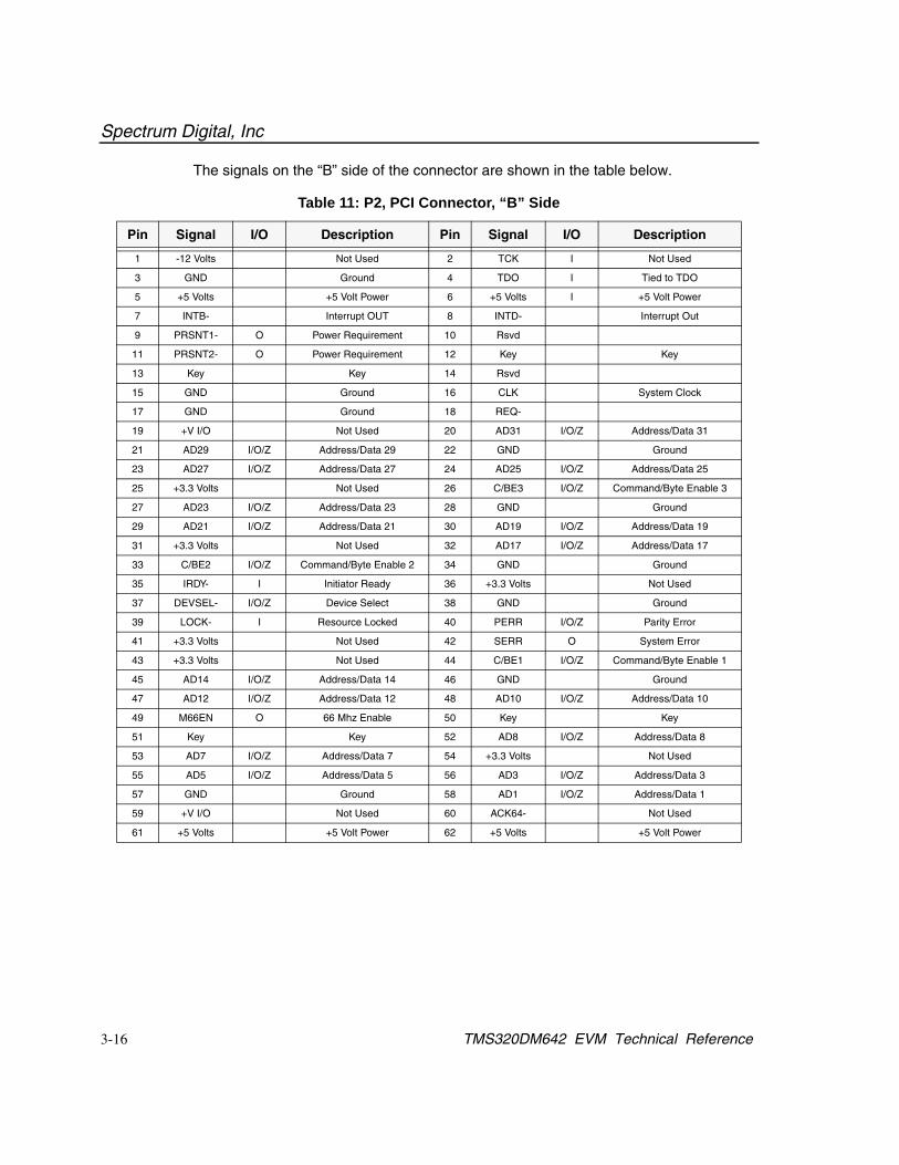
The signals on the “B” side of the connector are shown in the table below.
Table 11: P2, PCI Connector, “B” Side
Pin Signal I/O Description Pin Signal I/O Description
1 -12 Volts Not Used 2 TCK I Not Used
3 GND Ground 4 TDO I Tied to TDO
5 +5 Volts +5 Volt Power 6 +5 Volts I +5 Volt Power
7 INTB- Interrupt OUT 8 INTD- Interrupt Out
9 PRSNT1- O Power Requirement 10 Rsvd
11 PRSNT2- O Power Requirement 12 Key Key
13 Key Key 14 Rsvd
15 GND Ground 16 CLK System Clock
17 GND Ground 18 REQ-
19 +V I/O Not Used 20 AD31 I/O/Z Address/Data 31
21 AD29 I/O/Z Address/Data 29 22 GND Ground
23 AD27 I/O/Z Address/Data 27 24 AD25 I/O/Z Address/Data 25
25 +3.3 Volts Not Used 26 C/BE3 I/O/Z Command/Byte Enable 3
27 AD23 I/O/Z Address/Data 23 28 GND Ground
29 AD21 I/O/Z Address/Data 21 30 AD19 I/O/Z Address/Data 19
31 +3.3 Volts Not Used 32 AD17 I/O/Z Address/Data 17
33 C/BE2 I/O/Z Command/Byte Enable 2 34 GND Ground
35 IRDY- I Initiator Ready 36 +3.3 Volts Not Used
37 DEVSEL- I/O/Z Device Select 38 GND Ground
39 LOCK- I Resource Locked 40 PERR I/O/Z Parity Error
41 +3.3 Volts Not Used 42 SERR O System Error
43 +3.3 Volts Not Used 44 C/BE1 I/O/Z Command/Byte Enable 1
45 AD14 I/O/Z Address/Data 14 46 GND Ground
47 AD12 I/O/Z Address/Data 12 48 AD10 I/O/Z Address/Data 10
49 M66EN O 66 Mhz Enable 50 Key Key
51 Key Key 52 AD8 I/O/Z Address/Data 8
53 AD7 I/O/Z Address/Data 7 54 +3.3 Volts Not Used
55 AD5 I/O/Z Address/Data 5 56 AD3 I/O/Z Address/Data 3
57 GND Ground 58 AD1 I/O/Z Address/Data 1
59 +V I/O Not Used 60 ACK64- Not Used
61 +5 Volts +5 Volt Power 62 +5 Volts +5 Volt Power
Spectrum Digital, Inc
3-17
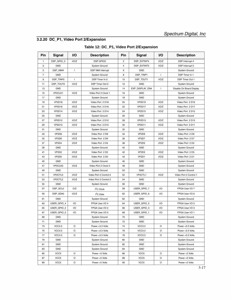
3.2.20 DC_P1, Video Port 2/Expansion
Table 12: DC_P1, Video Port 2/Expansion
Pin Signal I/O Description Pin Signal I/O Description
1 DSP_GPIO_3 I/O/Z DSP GPIO3 2 DSP_EXTINT4 I/O/Z DSP Interrupt 4
3 GND System Ground 4 DSP_EXTINT5 I/O/Z DSP Interrupt 5
5 DSP_NMI# I DSP NMI Interrupt 6 GND System Ground
7 GND System Ground 8 DSP_TINP1 I DSP Timer In 1
9 DSP_TINP0 I DSP Timer In 0 10 DSP_TOUT1 I/O/Z DSP Timer Out 1
11 DSP_TOUT0 I/O/Z DSP Timer Out 0 12 GND System Ground
13 GND System Ground 14 EXP_DISPLAY_EN# I Disable On Board Display
15 VP2CLK1 I/O/Z Video Port 2 Clock 1 16 GND System Ground
17 GND System Ground 18 GND System Ground
19 VP2D18 I/O/Z Video Port 2 D18 20 VP2D19 I/O/Z Video Port 2 D19
21 VP2D16 I/O/Z Video Port 2 D16 22 VP2D17 I/O/Z Video Port 2 D17
23 VP2D14 I/O/Z Video Port 2 D14 24 VP2D15 I/O/Z Video Port 2 D15
25 GND System Ground 26 GND System Ground
27 VP2D12 I/O/Z Video Port 2 D12 28 VP2D13 I/O/Z Video Port 2 D13
29 VP2D10 I/O/Z Video Port 2 D10 30 VP2D11 I/O/Z Video Port 2 D11
31 GND System Ground 32 GND System Ground
33 VP2D8 I/O/Z Video Port 2 D8 34 VP2D9 I/O/Z Video Port 2 D9
35 VP2D6 I/O/Z Video Port 2 D6 36 VP2D7 I/O/Z Video Port 2 D7
37 VP2D4 I/O/Z Video Port 2 D4 38 VP2D5 I/O/Z Video Port 2 D5
39 GND System Ground 40 GND System Ground
41 VP2D2 I/O/Z Video Port 2 D2 42 VP2D3 I/O/Z Video Port 2 D3
43 VP2D0 I/O/Z Video Port 2 D0 44 VP2D1 I/O/Z Video Port 2 D1
45 GND System Ground 46 GND System Ground
47 VP2CLK0 I/O/Z Video Port 2 Clock 0 48 GND System Ground
49 GND System Ground 50 GND System Ground
51 VP2CTL0 I/O/Z Video Port 2 Control 0 52 VP2CTL1 I/O/Z Video Port 2 Control 1
53 VP2CTL2 I/O/Z Video Port 2 Control 2 54 GND System Ground
55 GND System Ground 56 GND System Ground
57 DSP_SCL0 O/Z I2C Clock 58 USER_GPIO_7 I/O FPGA User I/O 7
59 DSP_SDA0 I/O/Z I2C Data 60 USER_GPIO_6 I/O FPGA User I/O 6
61 GND System Ground 62 GND System Ground
63 USER_GPIO_4 I/O FPGA User I/O 4 64 USER_GPIO_5 I/O FPGA User I/O 5
65 USER_GPIO_2 I/O FPGA User I/O 2 66 USER_GPIO_3 I/O FPGA User I/O 3
67 USER_GPIO_0 I/O FPGA User I/O 0 68 USER_GPIO_1 I/O FPGA User I/O 1
69 GND System Ground 70 GND System Ground
71 GND System Ground 72 GND System Ground
73 VCC3.3 O Power +3.3 Volts 74 VCC3.3 O Power +3.3 Volts
75 VCC3.3 O Power +3.3 Volts 76 VCC3.3 O Power +3.3 Volts
77 VCC3.3 O Power +3.3 Volts 78 VCC3.3 O Power +3.3 Volts
79 GND System Ground 80 GND System Ground
81 GND System Ground 82 GND System Ground
83 GND System Ground 84 GND System Ground
85 VCC5 O Power +5 Volts 86 VCC5 O Power +5 Volts
87 VCC5 O Power +5 Volts 88 VCC5 O Power +5 Volts
89 VCC5 O Power +5 Volts 90 VCC5 O Power +5 Volts
Spectrum Digital, Inc
3-18 TMS320DM642 EVM Technical Reference
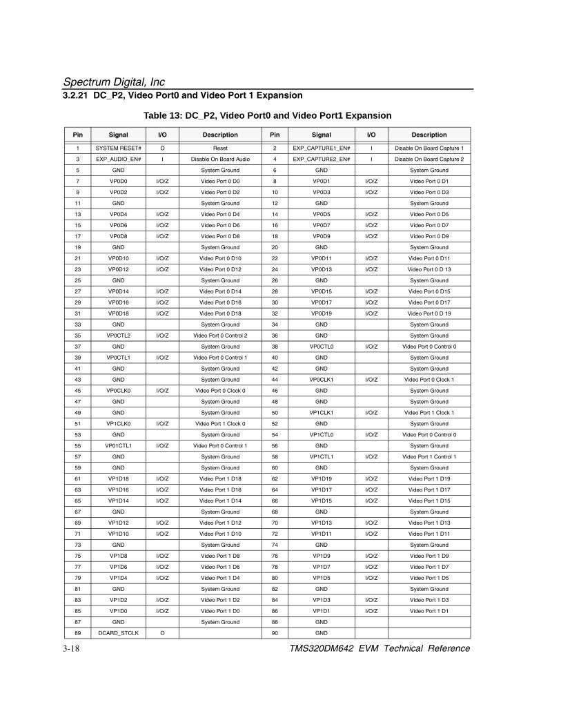
3.2.21 DC_P2, Video Port0 and Video Port 1 Expansion
Table 13: DC_P2, Video Port0 and Video Port1 Expansion
Pin Signal I/O Description Pin Signal I/O Description
1 SYSTEM RESET# O Reset 2 EXP_CAPTURE1_EN# I Disable On Board Capture 1
3 EXP_AUDIO_EN# I Disable On Board Audio 4 EXP_CAPTURE2_EN# I Disable On Board Capture 2
5 GND System Ground 6 GND System Ground
7 VP0D0 I/O/Z Video Port 0 D0 8 VP0D1 I/O/Z Video Port 0 D1
9 VP0D2 I/O/Z Video Port 0 D2 10 VP0D3 I/O/Z Video Port 0 D3
11 GND System Ground 12 GND System Ground
13 VP0D4 I/O/Z Video Port 0 D4 14 VP0D5 I/O/Z Video Port 0 D5
15 VP0D6 I/O/Z Video Port 0 D6 16 VP0D7 I/O/Z Video Port 0 D7
17 VP0D8 I/O/Z Video Port 0 D8 18 VP0D9 I/O/Z Video Port 0 D9
19 GND System Ground 20 GND System Ground
21 VP0D10 I/O/Z Video Port 0 D10 22 VP0D11 I/O/Z Video Port 0 D11
23 VP0D12 I/O/Z Video Port 0 D12 24 VP0D13 I/O/Z Video Port 0 D 13
25 GND System Ground 26 GND System Ground
27 VP0D14 I/O/Z Video Port 0 D14 28 VP0D15 I/O/Z Video Port 0 D15
29 VP0D16 I/O/Z Video Port 0 D16 30 VP0D17 I/O/Z Video Port 0 D17
31 VP0D18 I/O/Z Video Port 0 D18 32 VP0D19 I/O/Z Video Port 0 D 19
33 GND System Ground 34 GND System Ground
35 VP0CTL2 I/O/Z Video Port 0 Control 2 36 GND System Ground
37 GND System Ground 38 VP0CTL0 I/O/Z Video Port 0 Control 0
39 VP0CTL1 I/O/Z Video Port 0 Control 1 40 GND System Ground
41 GND System Ground 42 GND System Ground
43 GND System Ground 44 VP0CLK1 I/O/Z Video Port 0 Clock 1
45 VP0CLK0 I/O/Z Video Port 0 Clock 0 46 GND System Ground
47 GND System Ground 48 GND System Ground
49 GND System Ground 50 VP1CLK1 I/O/Z Video Port 1 Clock 1
51 VP1CLK0 I/O/Z Video Port 1 Clock 0 52 GND System Ground
53 GND System Ground 54 VP1CTL0 I/O/Z Video Port 0 Control 0
55 VP01CTL1 I/O/Z Video Port 0 Control 1 56 GND System Ground
57 GND System Ground 58 VP1CTL1 I/O/Z Video Port 1 Control 1
59 GND System Ground 60 GND System Ground
61 VP1D18 I/O/Z Video Port 1 D18 62 VP1D19 I/O/Z Video Port 1 D19
63 VP1D16 I/O/Z Video Port 1 D16 64 VP1D17 I/O/Z Video Port 1 D17
65 VP1D14 I/O/Z Video Port 1 D14 66 VP1D15 I/O/Z Video Port 1 D15
67 GND System Ground 68 GND System Ground
69 VP1D12 I/O/Z Video Port 1 D12 70 VP1D13 I/O/Z Video Port 1 D13
71 VP1D10 I/O/Z Video Port 1 D10 72 VP1D11 I/O/Z Video Port 1 D11
73 GND System Ground 74 GND System Ground
75 VP1D8 I/O/Z Video Port 1 D8 76 VP1D9 I/O/Z Video Port 1 D9
77 VP1D6 I/O/Z Video Port 1 D6 78 VP1D7 I/O/Z Video Port 1 D7
79 VP1D4 I/O/Z Video Port 1 D4 80 VP1D5 I/O/Z Video Port 1 D5
81 GND System Ground 82 GND System Ground
83 VP1D2 I/O/Z Video Port 1 D2 84 VP1D3 I/O/Z Video Port 1 D3
85 VP1D0 I/O/Z Video Port 1 D0 86 VP1D1 I/O/Z Video Port 1 D1
87 GND System Ground 88 GND
89 DCARD_STCLK O 90 GND
Spectrum Digital, Inc
3-19
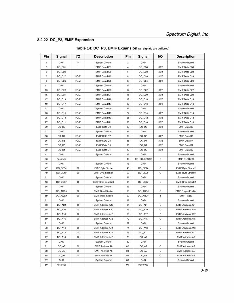
3.2.22 DC_P3, EMIF Expansion
Table 14: DC_P3, EMIF Expansion (all signals are buffered)
Pin Signal I/O Description Pin Signal I/O Description
1 GND O System Ground 2 GND System Ground
3 DC_D31 I EMIF Data D31 4 DC_D30 I/O/Z EMIF Data D30
5 DC_D29 EMIF Data D29 6 DC_D28 I/O/Z EMIF Data D28
7 DC_D27 I/O/Z EMIF Data D27 8 DC_D26 I/O/Z EMIF Data D26
9 DC_D25 I/O/Z EMIF Data D25 10 DC_D24 I/O/Z EMIF Data D24
11 GND System Ground 12 GND System Ground
13 DC_D23 I/O/Z EMIF Data D23 14 DC_D22 I/O/Z EMIF Data D22
15 DC_D21 I/O/Z EMIF Data D21 16 DC_D20 I/O/Z EMIF Data D20
17 DC_D19 I/O/Z EMIF Data D19 18 DC_D18 I/O/Z EMIF Data D18
19 DC_D17 I/O/Z EMIF Data D17 20 DC_D16 I/O/Z EMIF Data D16
21 GND System Ground 22 GND System Ground
23 DC_D15 I/O/Z EMIF Data D15 24 DC_D14 I/O/Z EMIF Data D14
25 DC_D13 I/O/Z EMIF Data D13 26 DC_D12 I/O/Z EMIF Data D12
27 DC_D11 I/O/Z EMIF Data D11 28 DC_D10 I/O/Z EMIF Data D10
29 DC_D9 I/O/Z EMIF Data D9 30 DC_D8 I/O/Z EMIF Data D8
31 GND System Ground 32 GND System Ground
33 DC_D7 I/O/Z EMIF Data D7 34 DC_D6 I/O/Z EMIF Data D6
35 DC_D5 I/O/Z EMIF Data D5 36 DC_D4 I/O/Z EMIF Data D4
37 DC_D3 I/O/Z EMIF Data D3 38 DC_D2 I/O/Z EMIF Data D2
39 DC_D1 I/O/Z EMIF Data D1 40 DC_D0 I/O/Z EMIF Data D0
41 GND System Ground 42 GND System Ground
43 Reserved 44 DC_ECLKOUT2 O EMIF CLKOUT2
45 GND System Ground 46 GND System Ground
47 DC_BE3# O EMIF Byte Strobe 48 DC_BE2# O EMIF Byte Strobe2
49 DC_BE1# O EMIF Byte Strobe1 50 DC_BE0# O EMIF Byte Strobe0
51 GND System Ground 52 GND System Ground
53 DC_CE3# O EMIF Chip Enable 3 54 DC_CE2# O EMIF Chip Select 2
55 GND System Ground 56 GND System Ground
57 DC_ARE# O EMIF Read Strobe 58 DC_AOE# O EMIF Output Enable
59 DC_AWE# O EMIF Write Strobe 60 DC_ARDY I EMIF Ready
61 GND System Ground 62 GND System Ground
63 DC_A22 O EMIF Address A22 64 DC_A21 O EMIF Address A21
65 DC_A20 O EMIF Address A20 66 DC_A19 O EMIF Address A19
67 DC_A18 O EMIF Address A18 68 DC_A17 O EMIF Address A17
69 DC_A16 O EMIF Address A16 70 DC_A15 O EMIF Address A15
71 GND System Ground 72 GND System Ground
73 DC_A14 O EMIF Address A14 74 DC_A13 O EMIF Address A13
75 DC_A12 O EMIF Address A12 76 DC_A11 O EMIF Address A11
77 DC_A10 O EMIF Address A10 78 DC_A9 EMIF Address A9
79 GND System Ground 80 GND System Ground
81 DC_A8 O EMIF Address A8 82 DC_A7 O EMIF Address A7
83 DC_A6 O EMIF Address A6 84 DC_A5 O EMIF Address A5
85 DC_A4 O EMIF Address A4 86 DC_A3 O EMIF Address A3
87 GND System Ground 88 GND System Ground
89 Reserved 90 Reserved
Spectrum Digital, Inc
3-20 TMS320DM642 EVM Technical Reference
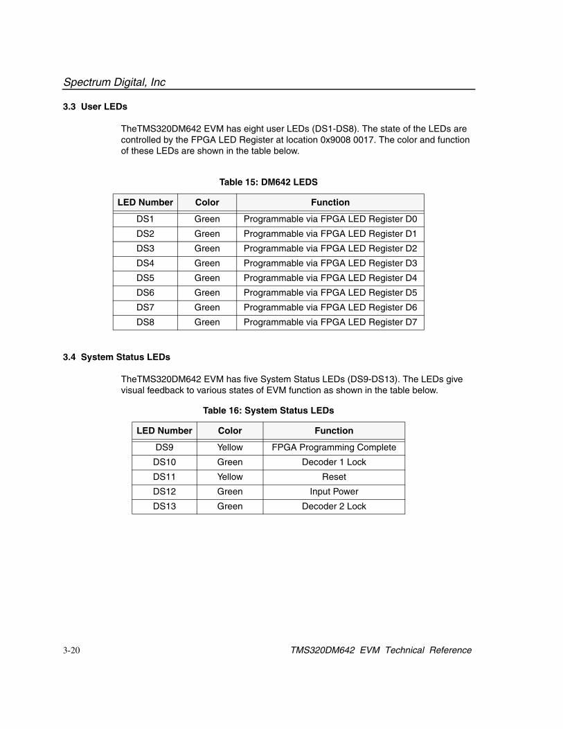
3.3 User LEDs
TheTMS320DM642 EVM has eight user LEDs (DS1-DS8). The state of the LEDs arecontrolled by the FPGA LED Register at location 0x9008 0017. The color and functionof these LEDs are shown in the table below.
3.4 System Status LEDs
TheTMS320DM642 EVM has five System Status LEDs (DS9-DS13). The LEDs givevisual feedback to various states of EVM function as shown in the table below.
Table 15: DM642 LEDS
LED Number Color Function
DS1 Green Programmable via FPGA LED Register D0
DS2 Green Programmable via FPGA LED Register D1
DS3 Green Programmable via FPGA LED Register D2
DS4 Green Programmable via FPGA LED Register D3
DS5 Green Programmable via FPGA LED Register D4
DS6 Green Programmable via FPGA LED Register D5
DS7 Green Programmable via FPGA LED Register D6
DS8 Green Programmable via FPGA LED Register D7
Table 16: System Status LEDs
LED Number Color Function
DS9 Yellow FPGA Programming Complete
DS10 Green Decoder 1 Lock
DS11 Yellow Reset
DS12 Green Input Power
DS13 Green Decoder 2 Lock
Spectrum Digital, Inc
3-21
3.5 Reset Switch - S3
There are three sources for reset on the TMS320DM642 EVM. The first reset is thepower on reset. This circuit waits until power is within the specified range beforereleasing the power on reset pin to the TMS320DM642.
The second source is the push button Reset switch, S3. When this button is pressedthe EVM is put through the reset state.
There is also an optional 2 pin Reset header, JP1, which is connected in parallel to theReset switch, S3. When this header is shorted the EVM is put into reset
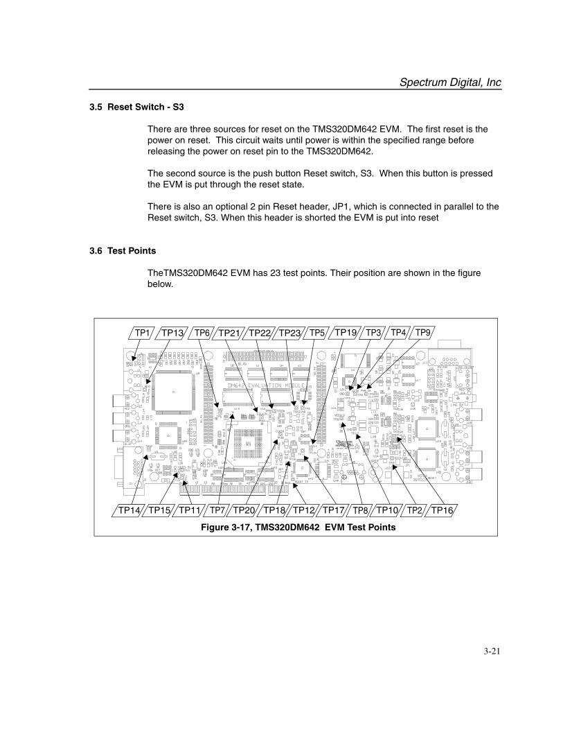
3.6 Test Points
TheTMS320DM642 EVM has 23 test points. Their position are shown in the figurebelow.
Figure 3-17, TMS320DM642 EVM Test Points
TP6 TP5 TP3 TP9TP1 TP13
TP14 TP15 TP11 TP8
TP21 TP22 TP23
TP20 TP18 TP12 TP17
TP19 TP4
TP10 TP2 TP16TP7
Spectrum Digital, Inc
3-22 TMS320DM642 EVM Technical Reference
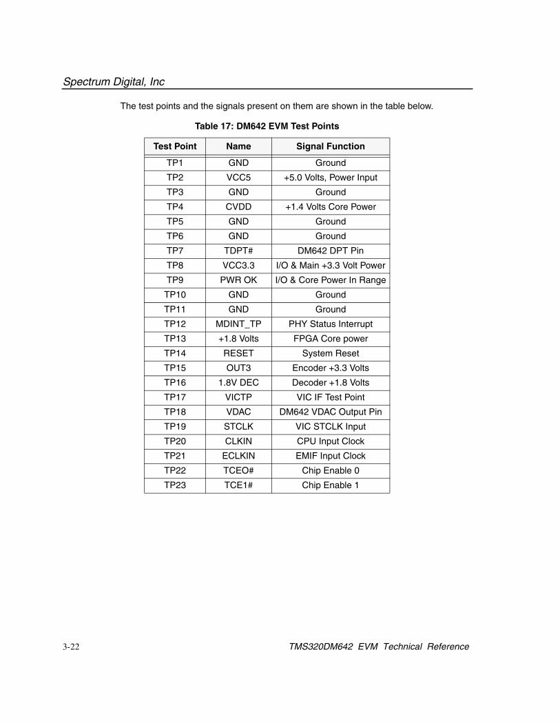
The test points and the signals present on them are shown in the table below.
Table 17: DM642 EVM Test Points
Test Point Name Signal Function
TP1 GND Ground
TP2 VCC5 +5.0 Volts, Power Input
TP3 GND Ground
TP4 CVDD +1.4 Volts Core Power
TP5 GND Ground
TP6 GND Ground
TP7 TDPT# DM642 DPT Pin
TP8 VCC3.3 I/O & Main +3.3 Volt Power
TP9 PWR OK I/O & Core Power In Range
TP10 GND Ground
TP11 GND Ground
TP12 MDINT_TP PHY Status Interrupt
TP13 +1.8 Volts FPGA Core power
TP14 RESET System Reset
TP15 OUT3 Encoder +3.3 Volts
TP16 1.8V DEC Decoder +1.8 Volts
TP17 VICTP VIC IF Test Point
TP18 VDAC DM642 VDAC Output Pin
TP19 STCLK VIC STCLK Input
TP20 CLKIN CPU Input Clock
TP21 ECLKIN EMIF Input Clock
TP22 TCEO# Chip Enable 0
TP23 TCE1# Chip Enable 1
A-1
Appendix A
Schematics
This appendix contains the schematics for the TMS320DM642 EVM.
Spectrum Digital, Inc
A-2 TMS320DM642 EVM Technical Reference
1 1
2 2
3 3
4 4
5 5
AA
BB
CC
DD
4.
ALL0.1
uFAND0.01uFCAPACITORS
AREDECOUPLING
CAPSUNLESS
OTHERWISENOTED.
THEYARE
SHOWNONTHEPAGEWITHTHEINTEGRATED
CIRCUITSTHEYSHOULDBEPLACEDNEAR.
NOTES,UNLESSOTHERWISESPECIFIED:
1.
RESISTANCEVALUES
INOHMS.
2.
CAPACTITANCE
VALUESIN
MICROFARADS.
3.
REFERENCEDESIGNATORSUSED:
5.
OBSERVE
THEFOLLOWINGLAYOUTNOTES:
1.
TOP-SIGNAL
ROUTING
2.
GROUNDPLANE
3.
INNER1-SIGNALROUTING
4.
VCC3PLANE(3.3VBOARD)
5.
INNER2-SIGNALROUTING
6.
INNER3-SIGNALROUTING
7.
VCCPLANE2
8.
INNER4-SIGNALROUTING
9.
GROUNDPLANE
10.
BOTTOM
-SIGNALROUTING
6.
BOARDPROPERTIES
B.
50+/-5OHMMATCHED
IMPEDANCE
C.
OUTER
LAYERS0.5OZCU/W
0.5OZAU
PLATING
D.
INNER
LAYERS1.0OZCU
E.
FR4BOARDMATERIAL
F.
MINIMUMTRACEWIDTH/SPACING4MILS
G.
MINIMUMVIASIZE10/19MIL
H.
LAYER
STACKUP:
A.
ROUTE
TOWITHIN
10%OFMANHATTANDISTANCE
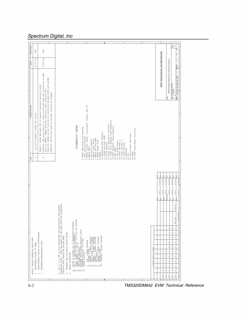
SCHEMATIC
INDEX
1DM642EVMNotesandContents
2UserOptions/Config
3DM642Clocks,Reset,Interrupts,Timers,andIIC
4DM642EMIF
5EmulationHeaders
6DM642Video
Ports
7DM642PCI/HPI/EMAC
8DM642Power
Pins
9SDRAM
10ExpansionEMIFBuffers
11Flash
andDualUART
12RS232
Buffers
13Video
Port
Expansion
Switches
14Video
Port
DaugherCardConnector
15EMIFDaughterCardConnector
16OSDFPGA
17OSDFPGAPower
18Video
Decoder1
19Video
Decoder2
20Video
Encoder
21Ethernet
22PCI
23AIC23
AudioInterface
24Power
25FPGAPower/ResetCircuitry
REV
ENGR
2REVISIONSTATUSOFSHEETS
111
SH
DATE
14
12
13
DATE
ENGR-MGR
MFG
7
DWN
DATE
8
DATE
10
SH
DATE
CHK
RLSE
APPLICATION
REV
35
NEXTASSY
DATE
6
DATE
9
QA
USED
ON
4
15
BA
BA
BA
AA
AA
AA
AA
A
R.R.P.
T.W.K.
R.R.P.
R.R.P.
C.M.D.
R.R.P.
R.R.P.
03/01/2004
03/01/2004
16
17
18
19
20
21
22
23
24
25
03/01/2004
03/01/2004
03/01/2004
03/01/2004
03/01/2004
REV
SH
AInitial
schematic
readyforlayout.
DESCRIPTION
REV
APPROVED
DATE
01/07/04
RRP
AA
AA
A
BA
AA
B
Sheet05:
Addquick
switchonJTAGtoprovidesomeESDprotectiontoEMU
pinsonDM642.AddedoptionalemulatorresetfrompinA15.
Sheet16:
AddedseriesterminationresistorsbetweenFPGAandencoder
10/01/04
RRP
B
Sheet3:Added
ANDgateU49tosupportoptionalemulatorreset.
Sheet20:
HDFiltersusedonencoder
outputsasshipped 50
7342
B
DM
642
Eva
luat
ion
Mod
ule
with
TI D
ecod
ers
(Ver
sion
3)
B
125
Thur
sday
, Dec
embe
r 02,
200
4
SPEC
TRU
M D
IGIT
AL IN
CO
RPO
RAT
ED
Title
Size
Doc
umen
t Num
ber
Rev
Dat
e:S
heet
of
Spectrum Digital, Inc
A-3
5 5
4 4
3 3
2 2
1 1
DD
CC
BB
AA
USER
LEDS
LED
S/S
WIT
CH
ES/C
ON
FIG
UR
ATI
ON
INPU
TS
SPDIFBLOCK
ON
ON
EMIF_ECLKINSEL[1:0]
NOPOP
1KOHM
ECLKIN(DEFAULT)
CPUCLOCK
/4
EMIFCLOCK
MODE
SELECTED
R42
R40
NO
POP
1K
OHM
1KOHM
1K
OHM
NOPOP
NO
POP
CPUCLOCK
/6
EMIFCLOCK
ECLKIN
OFF
NO
BOOT
(DEFAULT)
BOOT_MODE[1:0]
MODE
SELECTED
HPI/PCI
BOOT
MODE
S1-2
S1-1
OFF
OFF
ON
RESERVED
EMIF
8BITROM
BOOT
ON
ON
ON
OFF
LITTLEENDIAN
MODE
(DEFAULT)
BIG
ENDIANMODE
S2-2(ENDIAN)
OFF
ONENDIANMODECONFIGURATION
MODE
SELECTED
S2-1(PCI
ROM)
OFF
ON
PCIMODECONFIGURATION
MODE
SELECTED
PCI
EEPROMDISABLED(DEFAULT)
PCI
ROMENABLED
5073
42A
DM
642
Eva
luat
ion
Mod
ule
with
TI D
ecod
ers
(Ver
sion
3)
SPEC
TRU
M D
IGIT
AL. I
NC
OR
POR
ATED
B
225
Wed
nesd
ay, O
ctob
er 1
3, 2
004
Title
Size
Doc
umen
t Num
ber
Rev
Dat
e:S
heet
of
GN
D
USE
R_L
ED
0(1
6)U
SER
_LE
D1
(16)
USE
R_L
ED
2(1
6)U
SER
_LE
D3
(16)
USE
R_L
ED
4(1
6)U
SER
_LE
D5
(16)
USE
R_L
ED
6(1
6)U
SER
_LE
D7
(16)
BO
OT_
MO
DE
1(4
,10)
BO
OT_
MO
DE
0(4
,10)
LEN
DIA
N_M
OD
E(3
,14)
PC
I_E
EA
I(3
,14)
EM
IF_E
CLK
INS
EL0
(4,1
0)E
MIF
_EC
LKIN
SE
L1(4
,10)
SP
DIF
_OU
T(6
) EX
P_A
UD
IO_E
N#
(6,1
4) VC
C3.
3
GN
D
VCC
3.3
VC
C3.
3
VC
C3.
3
VC
C3.
3
VC
C3.
3
VCC
3.3
R11
4N
O P
OP
R42
NO
PO
PR
40N
O P
OP
R41
NO
PO
PR
44N
O P
OP
R22
150
C23
70.
1uF
J9R
CA
JAC
K
1
2
C23
80.
1uF
R19
110
0
R19
022
0
R18
150
R17
150
DS6 G
RE
EN
DS
5G
RE
EN
DS
7
GR
EEN
R22
01K
DS
8G
RE
EN
R16
150
R22
3N
O P
OP
R15
150
12
S2
DIP
_SW
ITC
H10
1184
-000
2
12
43
12
S1
DIP
_SW
ITC
H
1011
84-0
002
12
43
R90
1K
R89
1K
R11
5N
O P
OP
R21
9
1K
R22
1N
O P
OP
R21
150
R20
150
DS
1
GR
EEN
DS
2G
RE
EN
DS3 G
RE
END
S4
GR
EEN
R19
150
U34
SN
74LV
C1G
125
3
4
5
2
1
Spectrum Digital, Inc
A-4 TMS320DM642 EVM Technical Reference
1 1
2 2
3 3
4 4
5 5
AA
BB
CC
DD
DM
642
CLO
CK
S,R
ESE
TC
IRC
UIT
RY
,I2C
INTE
RFA
CE
3X
5.33X
8X
2.5X
3.33X
6X
2X
4X
5X
S1
S0
00
0 0
0 01 1
111
OPEN
OPEN
OPEN
OPEN
OPEN
OPEN
1
100
MHz
125
MHz
133.25MHz
62.5MHz
50
MHz
83.25
MHz
150
MHz
75
MHz
200
MHz
MULTIPLY
Pla
ce a
ll P
LL e
xter
nal c
ompo
nent
s as
clo
seto
the
DS
P. A
ll P
LL e
xter
nal c
ompo
nent
sm
ust b
e on
a s
ingl
e si
de o
f the
boa
rd.
I2C
RO
M
THISDESELECTS641
OPTION,
0AT
POWER
ON
RESET
OUTPUT
NO
POP
60Megahertz
Oscillatorfor
720MHzCPU
50Megahertz
Oscillatorfor
600MHzCPU
5073
42B
DM
642
Eva
luat
ion
Mod
ule
with
TI D
ecod
ers
(Ver
sion
3)
SPEC
TRU
M D
IGIT
AL IN
CO
RPO
RAT
ED
B
325
Frid
ay, O
ctob
er 2
2, 2
004
Title
Size
Doc
umen
t Num
ber
Rev
Dat
e:S
heet
of
DSP
_CLK
IN
DS
P_E
CLK
IN
DS
P_P
LL_V
DD
DS
P_P
LL_V
DD
DS
P_E
CLK
IN
GN
D
PC
I_E
EA
I(2
,14) DS
P_E
XTIN
T4(1
4)
DS
P_G
PIO
_3(2
,14)
EM
AC
_EN
ABLE
(7,1
4)
DS
P_E
XTIN
T5(1
4)
LEN
DIA
N_M
OD
E(2
,14)
DS
P_N
MI
(14)DS
P_E
XTIN
T7(1
6)
FPG
A_P
RO
G#
(17)
DS
P_S
CL0
(14,
18,1
9,20
,23)
DS
P_S
DA
0(1
4,18
,19,
20,2
3)
DS
P_T
OU
T1(2
,14)
DS
P_T
INP
1(1
4)
FPG
A_C
CLK
(17)
DS
P_T
INP
0(1
4)
FPG
A_D
IN(1
6)
DS
P_T
OU
T0(7
,14)
FPG
A_I
NIT
_EIN
T6(1
6)
VC
C3.
3
GN
D
FPG
A_L
OC
K(1
7)
SYS
TEM
_RE
SET#
(11,
14,1
6,17
,18,
19,2
0,21
,25)
EM
ULA
TOR
_RST
n(5
)
VC
C3.
3 VC
C3.
3
VC
C3.
3
VC
C3.
3
VC
C3.
3VC
C3.
3
VC
C3.
3
VCC
3.3
VC
C3.
3
VCC
3.3
VCC
3.3
VC
C3.
3
VC
C3.
3
C39
0.1u
F+
C40
10uF
E1
EXC
CE
T103
UE
MI F
ILTE
R
13
2
IO
GND
TP21
TP1
TP20
TP1
R66
2KR
672K
R17
4
NO
PO
P
R20
5N
O P
OP
R20
310
K
R17
336
0
R21
710
K
R17
1N
O P
OP
C11
90.
1uF
RN
27R
PA
CK
4-10
K
12345
678
C36
40.
1uF
R10
12K
C19
00.
1uF
R17
21K
C18
80.
1uF
R12
033
C18
6.0
01uF
C18
9N
O P
OP
L16
BLM
21P2
21S
N
U56
ICS
512
28 467
5
1 3VD
DX2
REF
S0
S1
CLK
X1/
ICLK
GN
D
R12
3N
O P
OP
R12
1N
O P
OP
R11
9N
O P
OP
R12
210
K
U26
60.0
0 M
Hz
4 321
VCC
OU
TG
ND
EN
R26
60
R25
1N
O P
OP
R26
70
R25
2N
O P
OP
R25
3N
O P
OP
R25
40
U21
25 M
Hz
4 321
VC
C
OU
TG
ND
EN
R11
8
33
C18
70.
1uF
L17
BLM
21P
221S
N
C18
4.0
01uF
R5
NO
PO
P
Clocks
/Interrupts
/
Timers
/IIC
RESERVED
U25
E
DM
642
AC2
AB
3
AA
2A
E4
AD3
AC4
D6
C6
F4 F3 F2 E1
M5 L5 B4
P4
AA
3
AF3V
6
E14
A4 C5
A5 B5 E4 D3
H25
CLK
IN
CLK
INF
CLK
MO
DE
0C
LKM
OD
E1
CLK
OU
TTC
LKO
UTF
GP
01 /
CLK
OU
T4G
P02
/ C
LKO
UT6
EX
TIN
T4 /
GP
04E
XTI
NT5
/ G
P05
EX
TIN
T6 /
GP
06E
XTI
NT7
/ G
P07
GP
00 /
DM
641S
EL
GP
03 /
PC
IEE
AI
NM
I
RES
ET
AM
UX
1
PLL
_LD
PLL
_VD
D
TSTS
TRB
TIN
P0
EM
AC
EN
/ TO
UT0
TIN
P1
LEN
DIA
N /
TOU
T1
SCL0
SD
A0
EC
LKIN
R91
33
U16 24
WC
256
18
436 5
27
A0
VC
C
VS
SN
CS
CL
SD
A
A1
WP
U20
ICS
512
28 467
5
1 3V
DDX2
RE
FS
0S
1C
LK
X1/
ICLK
GN
D
C31
30.
1uF
U49 SN
74LV
C1G
08
1 24
5 3
R21
836
0
R17
636
0
Spectrum Digital, Inc
A-5
1 1
2 2
3 3
4 4
5 5
AA
BB
CC
DD
NOTE4.1:PLACEALL
33-OHM
RESISTORS
AND
RESISTORNETWORKS
AS
CLOSEA
SPOSSIBLE
TO
THE
CORRESPONDING
U25
PINS.
NOTE:
ALTERNATEPIN
NAMES
DM
642
EMIF
AN
DTE
RM
INA
TOR
S50
7342
A
DM
642
Eva
luat
ion
Mod
ule
with
TI D
ecod
ers
(Ver
sion
3)
B
425
Wed
nesd
ay, O
ctob
er 1
3, 2
004
SPEC
TRU
M D
IGIT
AL IN
CO
RPO
RAT
ED
Title
Size
Doc
umen
t Num
ber
Rev
Dat
e:S
heet
of
TBE
5#
TBE
3#
TBE
6#TB
E7#
TBE
2#
TBE
4#
TBE
0#TB
E1#
DS
P_E
MU
1
DS
P_E
MU
4
ED
17
ED2
ED8
ED30
EA
12E
A13
ED38
ED48
DS
P_E
MU
0
ED
2
ED10
ED25
EA
19
ED39
ED
13
ED
15
ED
[0:3
1]
ED4
ED22
EA
11 BEz
4
DS
P_E
MU
6
ED
23
ED
7
ED18
BEz
7
EC
LKO
2
ED37
ED49
DS
P_T
MS
ED14
ED12
ED23
BEz
5
SD
CAS
z
ED33
ED53
ED
12
ED
1
ED
20
ED16ED17
ED29
DS
P_E
MU
9
ED
22
ED30
ED7
BEz
0
BEz
6
EC
LKO
1
ED50
DS
P_E
MU
5
DS
P_E
MU
11
ED
6
ED
19
ED8
ED6
ED20
EA
18
SD
RAS
z
SD
WE
z
ED35
ED54
ED
11
ED
31
ED
0
ED
25
ED
21
ED11
ED14
ED21
EA
16
EA
22
DSP
_TD
O
DS
P_E
MU
3
DS
P_E
MU
8
ED
29
ED1
ED15
BEz
3
PD
Tz
ED51
ED
4
ED
26
ED19
EA
17
ED55
ED
28
ED
10
ED
5
ED0
ED5
ED13
EA
15
ED32
DS
P_E
MU
7
DS
P_E
MU
10
ED24
ED9
ED24
EA
21 BEz
2
SO
E3z
ED52
DS
P_T
CLK
DS
P_T
DI
ED3
ED
27
ED
3
ED31
EA
14
ED36D
SP
_EM
U2
ED9
ED
18
ED
16
ED26ED27ED28
EA
20 BEz
1
SD
CKE
ED34
DS
P_T
RS
T#
TEA
17
TEA
15TE
A14
TEA
3
TEA
13TE
A12
TEA
11
TEA
21
TEA
5
TEA
19TE
A20
TEA
4
TEA
18
TEA
22
TEA
16
TEA
21
TEA
19TE
A20
TEA
22
GN
D
EA
3EA
3EA
4EA
5TE
A7
TEA
6TE
A10
TEA
9TE
A8
EA
4
EA
9E
A10
EA
6E
A5
EA7
EA6
EA
8E
A7
EA10
EA9
EA8
CE
0zC
E1z
CE
3zC
E2z
ED57
ED62
ED59
ED63
ED56
ED61ED60
ED58
TED
5
TED
30TE
D31
TED49
TED34
TED56
TED
6
TED
10
TED
27
ED41
TED
19
TED
16TED
9
TED
11
ED45
TED52
TED
4
TED
22
TED60
TED32
TED
7
TED
17
ED43
TED
12
ED47
TED61
TED35
TED57
TED
1
TED47TED46TED45TED44
TED
29
TED
24
TED
15
TED51
TED
13
TED53
TED63
TED54
TED62
TED
8
TED55
TED50
ED44
TED
25
TED48
TED58
TED33
TED43
TED40
TED
3
TED59
TED
0
ED46
TED
26
TED
21
TED
18
TED36
TED39
ED42TED41
TED
2
TED
28
TED37
TED
20
TED38
TED
14
TED
23
ED40
TED42
TBE
2#(9
,10)
TBE
3#(9
,10)
TBE
1#(9
,10)
TBE
0#(9
,10)
TBE
6#(9
)TB
E7#
(9)
TBE
4#(9
)TB
E5#
(9)
TEA
[3..2
2](2
,9,1
0)
TED
[0..6
3](9
,10)
TSD
RA
S#
(9,1
0)
TEC
LKO
UT2
(10)
TEC
LKO
UT1
(9)
TSD
CK
E(9
)
TPD
T#TS
OE
3#(1
1,16
)
TSD
WE
#(9
,10)
TSD
CA
S#
(9,1
0)
TCE
0#(9
)TC
E1#
(11,
16)
TCE
2#(1
0,11
)TC
E3#
(10,
11)
TEA
RD
Y(1
0)
DS
P_E
MU
1(5
)D
SP
_EM
U0
(5)
DS
P_E
MU
2(5
)D
SP
_EM
U3
(5)
DS
P_T
CLK
(5)
DS
P_T
DI
(5)D
SP_T
RST
#(5
)
DS
P_T
DO
(5)
DS
P_T
MS
(5) D
SP
_EM
U5
(5)
DS
P_E
MU
8(5
)
DS
P_E
MU
4(5
)
DS
P_E
MU
9(5
)
DS
P_E
MU
6(5
)D
SP
_EM
U7
(5)D
SP
_EM
U11
(5)
DS
P_E
MU
10(5
)
BOO
T_M
OD
E1
(2,1
0)BO
OT_
MO
DE
0(2
,10)
EMIF
_EC
LKIN
SEL0
(2,1
0)EM
IF_E
CLK
INSE
L1(2
,10)
VCC
3.3
GN
D
TSD
WE
#(9
,10)
TAO
E#
(9,1
0)TS
DC
AS
#(9
,10)
TAW
E#
(9,1
0)
TSD
RA
S#
(9,1
0)TA
RE
#(9
,10)
VC
C3.
3
VC
C3.
3
RN5
RPACK8-33
12345678 9
10111213141516
R97
33
RN
17R
PA
CK
8-33
1 2 3 4 5 6 7 8910111213141516
RN
1R
PA
CK
8-33
1 2 3 4 5 6 7 8910111213141516
R94
33
RN6
RPACK8-33
12345678 9
10111213141516
R98
33
R92
10K
R37
4.7K
RN
8R
PAC
K8-3
31 2 3 4 5 6 7 8
910111213141516
RN
7R
PAC
K8-3
31 2 3 4 5 6 7 8
910111213141516
R96
33
TP23
TP1
TP22
TP1
EMIF
and
Emulation
U25
A
DM
642
B24A24B23B22C22A23C21B21
D21A21C20B20D20A20D19C19
H24H23G26G23G25G24F26F23
F25F24E25E24D25D26C25C26
M24
M23
N26
N24
N23
P26
P24
P23
R24
R23
T25
T24
U26
U25
U24
V23
V26
V25
V24
U23
L24
L23
M26
M25
R26
R25
T23
T22
K25
K24
K23
L26
J24
J25
K26
L25
R22
M22
J26
J23
N22
P22
AD26AD25AC25AC26AB24AB25AB23AA24
AA25AA23AA26Y24Y25Y23Y26W23
AD19AC19AF20AC20AE20AD20AF21AC21
AE21AD21AE22AD22AD23AE23AF23AF24
W24L2
2
E15
A18
A16
D14
B18
A15
C14
B15
C15
D15
B16
C16
A17
D16
B17
C17
D17
ED0ED1ED2ED3ED4ED5ED6ED7
ED8ED9
ED10ED11ED12ED13ED14ED15
ED16ED17ED18ED19ED20ED21ED22ED23
ED24ED25ED26ED27ED28ED29ED30ED31
EA
03E
A04
EA
05E
A06
EA
07E
A08
EA
09E
A10
EA
11E
A12
EA
13E
A14
EA
15E
A16
EA
17E
A18
EC
LKIN
SEL0
/ E
A19
EC
LKIN
SEL1
/ E
A20
BO
OTM
OD
E0
/ EA2
1B
OO
TMO
DE
1 / E
A22
BE
0B
E1
BE
2B
E3
BE
4B
E5
BE
6B
E7
CE
0C
E1
CE
2C
E3
SD
RA
S/A
OE
SD
CA
S/A
RE
SDW
E/A
WE
SDC
KE
SO
E3
PD
T
ECLK
OU
T1EC
LKO
UT2
HO
LDA
BUS
RE
Q
ED32ED33ED34ED35ED36ED37ED38ED39
ED40ED41ED42ED43ED44ED45ED46ED47
ED48ED49ED50ED51ED52ED53ED54ED55
ED56ED57ED58ED59ED60ED61ED62ED63
HO
LD
AR
DY
TMS
TDI
TCLK
TRST
TDO
EM
U0
EM
U1
EM
U2
EM
U3
EM
U4
EM
U5
EM
U6
EM
U7
EM
U8
EM
U9
EM
U10
EM
U11
R12
733R
N16
RPA
CK4
-33
1 2 3 45678
RN
2R
PAC
K8-3
31 2 3 4 5 6 7 8
910111213141516
RN11
RPACK8-33
12345678 9
10111213141516
R95
33
RN12
RPACK8-33
12345678 9
10111213141516
RN
15R
PAC
K8-3
31 2 3 4 5 6 7 8
910111213141516
R93
33RN
13R
PAC
K4-3
31 2 3 4
5678
RN
14R
PA
CK
8-33
123456789 10 11 12 13 14 15 16
R12
633
TP7
TP1
Spectrum Digital, Inc
A-6 TMS320DM642 EVM Technical Reference
DSPJTAG
HEADER
ROU
TE T
RAC
ES A
SO
NE G
ROUP
. MAT
CHSI
GNA
L LE
NG
TH.
LOC
ATE
R-P
AC
K N
EA
R D
SP
EM
ULA
TIO
N
J1 A
ND J
2 N
EED
TOBE
AS
CLO
SETO
GET
HER
ASPH
YSIC
ALLY
POSS
IBLE
5068
42B
DM
642
Eva
luat
ion
Mod
ule
with
TI D
ecod
ers
(Ver
sion
3)
SPEC
TRU
M D
IGIT
AL IN
CO
RPO
RAT
ED
B
525
Wed
nesd
ay, O
ctob
er 1
3, 2
004
Title
Siz
eD
ocum
ent N
umbe
rR
ev
Dat
e:S
heet
of
HU
R_E
MU
9H
UR
_EM
U8
HU
R_E
MU
5H
UR
_EM
U4
HU
R_E
MU
7H
UR
_EM
U6
HU
R_E
MU
11
HU
R_E
MU
2H
UR
_EM
U3
HU
R_E
MU
10
HU
R_E
MU
1X
DS
_TR
ST#
GN
D
B.X
DS_
EM
U0
XD
S_T
CK
B.X
DS_
TCK
B.X
DS_
TMS
XD
S_TD
I
XD
S_E
MU
0
B.X
DS_
TDO
B.X
DS
_EM
U0
XD
S_E
MU
0
XD
S_T
MS
B.X
DS
_EM
U1
XD
S_E
MU
1
XD
S_T
DO
B.X
DS_
TDI
XD
S_T
DO
HU
R_E
MU
0X
DS
_TD
I
XD
S_E
MU
1
B.X
DS
_TC
KRE
TH
UR
_TC
KR
TN
B.X
DS_
EM
U1
B.X
DS_
TCK
RE
T
XD
S_T
CK
RE
T
XDS
_TR
ST#
XD
S_T
CK
HU
R_T
CK
XD
S_TM
S
XD
S_T
CK
RE
T
B.X
DS_
TRS
T#
DSP
_TD
O(4
)
DSP
_TD
I(4
)
DSP
_TM
S(4
)
DS
P_E
MU
9(4
)D
SP
_EM
U8
(4)
DS
P_E
MU
2(4
)
DS
P_E
MU
7(4
)
DS
P_E
MU
3(4
)
DS
P_E
MU
5(4
)D
SP
_EM
U4
(4)
DS
P_E
MU
6(4
)
DS
P_E
MU
0(4
)
DS
P_E
MU
1(4
)
DS
P_E
MU
10(4
)D
SP
_EM
U11
(4)
DS
P_T
CLK
(4)
DSP
_TR
ST#
(4)
GN
D
VCC
3.3
EM
ULA
TOR
_RS
Tn(3
)
VC
C3.
3
VC
C3.
3
VC
C3.
3
VC
C3.
3
VC
C3.
3
VC
C3.
3
VC
C3.
3
VC
C3.
3
VC
C3.
3
VC
C3.
3
R27
210
K
R18
31K
R24
4N
O-P
OP
U31
SN
74LV
C1G
32
1 24
5 3
RN
3D39
RN
4C39
RN
3E39
RN
4D39
R18
033
R17
833
U30 SN
74LV
C1G
321 2
4
5 3
RN
4A39
RN
4B39
R17
910
0 1%
C27
90.
1uF
J7
HE
AD
ER
7x2
, Em
ulat
ion
1 3 5 7 9
2 4 8 1011
1213
14
C28
0
18pF
J19
HE
AD
ER
4x1
5
A1
A2
A3
A4
A5
A6
A7
A8
A9
A10
A11
A12
A13
A14
A15
D1
D2
D3
D4
D5
D6
D7
D8
D9
D10
D11
D12
D13
D14
D15
B14
C14
B13
C13
B12
C12
B11
C11
B10
C10B9
C9
B7
C7
B6
C6
B5
C5
B4
C4
B3
C3
B2
C2
B1
B15C1
C15 B8
C8
GN
DG
ND
GN
DG
ND
GN
DG
ND
GN
DTY
PE0
GN
DG
ND
GN
DG
ND
GN
DG
ND
TGTR
ST
GN
DG
ND
GN
DG
ND
GN
DG
ND
GN
DTY
PE1
GN
DG
ND
GN
DG
ND
GN
DG
ND
GN
D
EM
U0
EM
U1
EM
U2
EM
U3
TCLK
EM
U4
EM
U5
EM
U6
EM
U7
EM
U8
EM
U9
EM
U10
TDO
EM
U11
EM
U12
EM
U13
EM
U14
EM
U15
TDI
EM
U16
EM
U17
TRS
TnTM
S
EM
U18
ID0
ID1
ID2
ID3
TVD
TCK
RTN
RN
3G39
RN
3F39
RN
4H39
RN
3B39
RN
3A39
RN
3C39
RN
4G39
RN
4F39
RN
4E39
R17
71K
C37
10.
1uF
R27
5N
O-P
OP
R27
4N
O-P
OP
R27
6N
O-P
OP
R27
70
U57
74C
BTL
V324
5A
218
317
416
515
614
713
812
911
19 120 10
A1
B1
A2
B2
A3
B3
A4
B4
A5
B5
A6
B6
A7
B7
A8
B8
G NC
VC
C
GN
D
RN
3H39
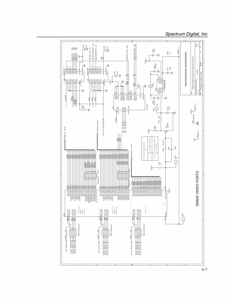
Spectrum Digital, Inc
A-7
1 1
2 2
3 3
4 4
5 5
AA
BB
CC
DD
DM
642
VID
EO
PO
RTS
PCISPEEDCONFIGURATION
R170
1K
NO
POP
PCIENABLED
@66MHZ
ORDISABLED
PCIENABLED
@33MHZ
5073
42A
DM
642
Eva
luat
ion
Mod
ule
with
TI D
ecod
ers
(Ver
sion
3)
SPEC
TRU
M D
IGIT
AL IN
CO
RPO
RAT
ED
B
625
Wed
nesd
ay, O
ctob
er 1
3, 2
004
Title
Size
Doc
umen
t Num
ber
Rev
Dat
e:S
heet
of
VP2
D11
VP2
D0
VP2
D4
VP2
D12
VP2
D7
VP2
D5
VP2
D13
VP2
D1
VP2
D6
VP2
D14
VP2
D16
VP2
D2
VP2
D10
VP2
D17
VP2
D8
VP2
D15
VP2
D9
VP2
D18
VP2
D19
VP2
D3
STC
LK
STC
LK
GN
D
4.1V
VP
0D6
VP
0D19
AH
CLK
X0
VP
0D15
AM
UTE
IN
VP
0D1
VP
0D4
VP
0D10
VP
0D9
AH
CLK
X0
VP
0D7
VP
0D12
AC
LKR
0
VP
0D14
AH
CLK
R0
VP
0D8
VP
0D13
AFS
R0
VP
0D17
AC
LKX0
VP
0D0
VP
0D5
VP
0D2
VP
0D11
VP
0D16
AM
UTE
VP
0D18
AFS
X0
VP
0D3
AC
LKR
0A
FSR
0AFS
X0
AC
LKX
0
VP
1D8
VP
1D5
AXR
2
VP
1D6
VP
1D10
VP
1D9
VP
1D7
VP
1D4
VP
1D1
VP
1D15
AX
R3
VP
1D17
AX
R5
VP
1D14
AX
R2
VP
1D13
AX
R1
VP
1D11
VP
1D2
VP
1D16
AX
R4
VP
1D18
AX
R6
VP
1D0
VP
1D19
AX
R7
AXR
1A
XR0
VP
1D12
AX
R0
VP
1D3
AX
R0
AX
R1
AX
R2
VP
1CTL
2(1
3,14
)
VP
1D[0
:19]
(13,
14)
VP
1CTL
0(1
3,14
)V
P1C
LK0
(13,
14)
VP
1CTL
1(1
3,14
)
VP
1CLK
1(1
4)
VP
2D[0
..19]
(13,
14)
VP0D
[0..1
9](1
3,14
)
VP0C
TL0
(13,
14)
VP0C
TL2
(13,
14)
VP0C
LK1
(14)
VP0C
LK0
(13,
14)
VP0C
TL1
(13,
14) V
P2C
TL0
(13,
14)
VP
2CLK
1(1
3,14
)
VP
2CTL
2(1
3,14
)V
P2C
TL1
(13,
14)
VP
2CLK
0(1
3,14
)
PLL
_MS
(16)
PLL
_MD
(16)
PLL
_MC
(16)E
XP
_AU
DIO
_EN
#(2
,14)
BC
LK2
(23)
LRC
OU
T(2
3)
AIC
23_S
TCLK
(23)
SA
A71
05_S
TCLK
(20)
DC
AR
D_S
TCLK
(14)
VCC
3.3
G
ND
4.1V
(13,
25)
BC
LK1
(23)
AIC
23SD
ATA
OU
T(2
3)
LRC
IN(2
3)
AIC
23SD
ATA
IN(2
3)
SP
DIF
_OU
T(2
)
VC
C3.
3
VC
C3.
3
4.1V
VCC
3.3
VC
C3.
3
VC
C3.
3
VC
C3.
3
4.1V
4.1V
R11
210
K
Video
Port
0
McBSP0
McASP
Control
Video
Port
1
McBSP1
McASP
Data
Video
Port
2
VIC
U25
B
DM
642A
F18
AE
18A
F17
AF1
6A
E16
AD
16A
C16
AB
16A
E15
AD
15A
C15
AB
15A
D14
AC
14A
B14
AD
13A
C13
AB
13A
D12
AC
12
AF5
AF6
AE
6A
D6
AC
6A
E7
AD
7A
C7
AD
8A
C8
AE
9A
D9
AC
9A
D10
AC
10A
E11
AD
11A
C11
AB
11A
B12
AF1
4A
F12
AE
17A
C17
AD
17
AF8
AF1
0
AF4
AE5
AD
5
C8
D8
A9
B9
C9
D9
A10
B10
C10
D10
A11
B11
C11
D11
E11
B12
C12
D12
E12
E13
A7 A13 B8 D7
C7
AD
1A
C1
VP0
_D00
VP0
_D01
CLK
X0/V
P0_
D02
FSX
0/V
P0_
D03
DX
0/VP
0_D
04C
LKS0
/VP
0_D
05D
R0/
VP0
_D06
FSR
0/V
P0_
D07
CLK
R0/
VP
0_D
08V
P0_D
09V
P0_D
10V
P0_D
11A
CLK
R0/
VP
0_D
12A
FSR
0/V
P0_
D13
AH
CLK
R0/
VP
0_D
14A
MU
TEIN
/VP
0_D
15A
MU
TE/V
P0_
D16
AC
LKX
0/V
P0_D
17A
FSX0
/VP
0_D
18A
HC
LKX
0/V
P0_D
19
VP1
_D00
VP1
_D01
CLK
X1/V
P1_
D02
FSX
1/V
P1_
D03
DX
1/VP
1_D
04C
LKS1
/VP
1_D
05D
R1/
VP1
_D06
FSR
1/V
P1_
D07
CLK
R1/
VP
1_D
08V
P1_D
09V
P1_D
10V
P1_D
11A
XR
0/V
P1_
D12
AX
R1/
VP
1_D
13A
XR
2/V
P1_
D14
AX
R3/
VP
1_D
15A
XR
4/V
P1_
D16
AX
R5/
VP
1_D
17A
XR
6/V
P1_
D18
AX
R7/
VP
1_D
19
VP
0_C
LK0
VP
0_C
LK1
VP
0_C
TL0
VP
0_C
TL1
VP
0_C
TL2
VP
1_C
LK0
VP
1_C
LK1
VP
1_C
TL0
VP
1_C
TL1
VP
1_C
TL2
VP2
_D00
VP2
_D01
VP2
_D02
VP2
_D03
VP2
_D04
VP2
_D05
VP2
_D06
VP2
_D07
VP2
_D08
VP2
_D09
VP2
_D10
VP2
_D11
VP2
_D12
VP2
_D13
VP2
_D14
VP2
_D15
VP2
_D16
VP2
_D17
VP2
_D18
VP2
_D19
VP
2_C
LK0
VP
2_C
LK1
VP
2_C
TL0
VP
2_C
TL1
VP
2_C
TL2
VD
AC
/ G
P08
STC
LK
RN
23R
PA
CK
8-33
123456789 10 11 12 13 14 15 16
C24
40.
1uF
R17
533
R17
01K
U54
74C
BT3
245A
218
317
416
515
614
713
812
911
19 120 10
A1
B1
A2
B2
A3
B3
A4
B4
A5
B5
A6
B6
A7
B7
A8
B8
G NC
VC
C
GN
D
RN
22R
PA
CK
8-33
1 2 3 4 5 6 7 8910111213141516
C34
5N
O P
OP
C34
4N
O P
OP
U27
PLL
1708
11310 11
20 84167 6 5
19 917 3 182 15 14
12
VD
D1
VD
D2
XT1
XT2
VD
D3
VC
C
DG
ND
1D
GN
D2
MS
MC
MD
SCK
O1
AG
ND
DG
ND
3
SCK
O3
SCK
O0
SCK
O2
MC
KO
2M
CK
O1
CSE
L
RN
20R
PAC
K4-
33
1 2 3 45678
C24
20.
1uF
C24
5
100p
F
Q2
2N39
04
R16
922
.1K
1%
R16
6
33
R16
710
0K
R16
82.
2K
R16
433
R16
533
R11
633
R11
733
U28
74C
BT3
245A
218
317
416
515
614
713
812
911
19 120 10
A1
B1
A2
B2
A3
B3
A4
B4
A5
B5
A6
B6
A7
B7
A8
B8
G NC
VC
C
GN
D
C34
0
0.1u
F
Y2
27M
Hz
C18
2
0.1u
F
TP17
TP1
U32 PI
6CX
100-
27W
18
436 5
27
X1
X2
GN
DV
INVD
DC
LKO
UT
NC
1N
C2
TP19
TP1
TP18
TP1
C18
5
0.1u
F
C24
3
10pF
R12
433
R12
533
RN
21R
PAC
K4-
33
1 2 3 45678
RN
24R
PAC
K4-
33
1 2 3 45678
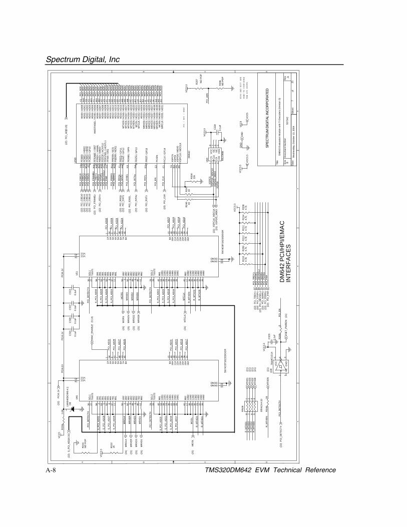
Spectrum Digital, Inc
A-8 TMS320DM642 EVM Technical Reference
1 1
2 2
3 3
4 4
5 5
AA
BB
CC
DD
DM
642
PC
I/HP
I/EM
AC
INTE
RFA
CES
R206
AND
R207
ARE
USED
TO
CONFIGURE
THE
HPI
WIDTH
5073
42A
DM
642
Eva
luat
ion
Mod
ule
with
TI D
ecod
ers
(Ver
sion
3)
SPEC
TRU
M D
IGIT
AL IN
CO
RPO
RAT
ED
B
725
Wed
nesd
ay, O
ctob
er 1
3, 2
004
Title
Size
Doc
umen
t Num
ber
Rev
Dat
e:S
heet
of
PCI_
AD
24
PCI_
AD
30
PCI_
AD
28
PCI_
AD
16
PCI_
AD
18
PCI_
AD
20
PCI_
AD
22PC
I_A
D21
PCI_
AD
19
PCI_
AD
17
PCI_
AD
23
PCI_
AD
27
PCI_
AD
31
PC
I_FR
AM
Ez
PC
I_TR
DY
z
PC
I_S
TOP
z
PC
I_P
AR
PC
I_C
BEz
0
PC
I_C
BEz
3
PC
I_IR
DY
z
PC
I_D
EVS
ELz
PC
I_P
ER
Rz
PC
I_S
ER
Rz
PC
I_C
BEz
1
PC
I_R
EQ
zP
CI_
GN
Tz
PC
I_ID
SEL
PC
I_IN
TAz
PC
I_R
STz
PC
I_C
LK
PCI_
AD
26PC
I_A
D25
PCI_
AD
29
PC
I_C
BEz
2
PC
I_A
D21
PC
I_A
D29
R_M
TXD
3
MR
XE
R
MR
XD
1
MR
CLK
MC
OL
PC
I_A
D19
PC
I_A
D17
PC
I_A
D27
PC
I_A
D31
R_M
TXD
1
MR
XD
3
PC
I_A
D25
PC
I_E
N
S_P
CI_
AD
25
S_P
CI_
AD
29
S_P
CI_
AD
27
S_P
CI_
AD
31
S_P
CI_
AD19
S_P
CI_
AD17
S_P
CI_
AD
21
PC
I_D
ETE
CT#
S_P
CI_
AD
23
PC
I_A
D23
PCI_
AD
4
PCI_
AD
0
PCI_
AD
2PC
I_A
D1
PCI_
AD
15
PCI_
AD
13
PCI_
AD
3
PCI_
AD
10PC
I_A
D11
PCI_
AD
5
PCI_
AD
8PC
I_A
D9
PCI_
AD
12
PCI_
AD
7PC
I_A
D6
PCI_
AD
14
PC
I_A
D5
PC
I_D
ETE
CT#
MR
XD
0
PCI_
AD
30
S_P
CI_
AD
28
R_M
TXD
2
PC
I_A
D16
PC
I_A
D18
PCI_
AD
28S
_PC
I_A
D24
PC
I_A
D22
S_P
CI_
AD
30
PC
I_A
D20
S_P
CI_
AD
16
S_P
CI_
AD
22
R_M
TXEN
PCI_
AD
24M
CR
S
S_P
CI_
AD
26
R_M
TXD
0
PC
I_D
ETE
CT#
S_P
CI_
AD
20
MR
XD
V
S_P
CI_
AD
18
MTC
LK
PC
I4.1
V
PCI_
AD
26
MR
XD
2
PC
I4.1
VP
CI4
.1V
PC
I_D
ETE
CT#
XS
PCS
GN
D
XS
PD
I
PCI_
PA
R
PCI_
DEV
SE
LzPC
I_S
TOP
zPC
I_TR
DY
z
PCI_
SE
RR
zPC
I_P
ER
Rz
PC
I_D
ETE
CT#
PC
I_E
N
R_M
TXD
3R
_MTX
D1
R_M
TXD
2R
_MTX
D0
R_M
TXEN
XS
PD
O_M
DIO
XS
PC
LK_M
DC
LK
S_P
CI_
AD
[16:
31]
(22)
PC
I_AD
[0:1
5](2
2)
PCI_
CBE
z0(2
2)PC
I_C
BEz1
(22)
PCI_
CBE
z2(2
2)PC
I_C
BEz3
(22)
PCI_
REQ
z(2
2)PC
I_G
NTz
(22)
PC
I_ID
SE
L(2
2)
PCI_
INTA
z(2
2)PC
I_FR
AM
Ez(2
2)
PCI_
IRD
Yz
(22)
PCI_
RST
z(2
2)
PC
I_C
LK(2
2)
MC
OL
(21)
MR
CLK
(21)
MR
XE
R(2
1)
MR
XD
3(2
1)
MR
XD
1(2
1)
PC
I_D
ETE
CT#
(22)
EN
ET_
PWR
DN
(21)
VC
C3.
3
GN
D
VCC
5
PC
I4.1
V(2
2)
MC
RS
(21)
MR
XD
0(2
1)
MR
XD
2(2
1)
MR
XD
V(2
1)
MTC
LK(2
1)
XSP
CLK
_MD
CLK
(21)
XS
PDO
_MD
IO(2
1)
PCI_
TRD
Yz
(22)
PCI_
STO
Pz
(22) P
CI_
DE
VSE
Lz(2
2)
PCI_
PE
RR
z(2
2)PC
I_S
ER
Rz
(22)
PC
I_P
AR
(22)
MTX
D3
(21)
MTX
D1
(21)
MTX
D2
(21)
MTX
D0
(21)
MTX
EN(2
1)
EM
AC
_EN
AB
LE(3
,14)
VCC
3.3
VC
C5
VC
C3.
3V
CC
5
VC
C3.
3
VC
C3.
3
VCC
3.3
VC
C3.
3
U51
SN
74C
BT16
233D
GG
R
56
1
30
14
1344
27 2 53 5 50 8 47 11 55 3 52 6 49 9 46 12
54 4 51 7 48 10 45
29 28 42 16 39 19 36 22 33 25 41 17 38 20 35 23 32 26
15 40 18 37 21 34 24 31
43
1B1
1A
SE
L1
VCC
DGNDDGND
TES
T1
2B1
3B1
4B1
5B1
6B1
7B1
8B1
1B2
2B2
3B2
4B2
5B2
6B2
7B2
8B2
2A 3A 4A 5A 6A 7A 8A
SE
L2TE
ST2
9B1
10B
111
B1
12B
113
B1
14B
115
B1
16B
1
9B2
10B
211
B2
12B
213
B2
14B
215
B2
16B
2
9A 10A
11A
12A
13A
14A
15A
16A
VCC
R24
633
R24
733
R24
833
U39
74A
HC
1G14
42
5 31
YA
VC
C
GN
DN
C
U50 93
LC66
B
1 2 3 4678 5
CS
CLK
DI
DO
NC
NC
VC
C
VS
S
R21
44.
7k
R20
410
k
C33
6
0.1u
F
R20
7
NO
PO
P
R20
6N
O P
OP
PCI
/HPI
/EMAC
U25
D DM
642
Y3
AA
1
Y2
W3
Y1
W4
W2
V2
V3
Y4
V1
U4
U2
U3
U1
T3 M3
M2
M4
L2 L3 K2
L4 K1
K4
J1 J3 H2
J4 G2
H3
G1
R2T2 N3
N4
M1
N1
V4
E2J2 F1 H4
G4
C1
G3K3
P3
R3
P1
R1 T4 R4
P5
R5
HD
00 /
AD
00H
D01
/ A
D01
HD
03 /
AD
03H
D04
/ A
D04
HW
DTH
SE
L / H
D05
/ A
D05
HD
06 /
AD
06H
D07
/ A
D07
HD
08 /
AD
08H
D09
/ A
D09
HD
02 /
AD
02
HD
10 /
AD
10H
D11
/ A
D11
HD
12 /
AD
12H
D13
/ A
D13
HD
14 /
AD
14H
D15
/ A
D15
MTX
D0
/ HD
16 /
AD
16M
TXD
1 / H
D17
/ A
D17
MTX
D2
/ HD
18 /
AD
18M
TXD
3 / H
D19
/ A
D19
MTX
EN
/ H
D20
/ A
D20
MC
OL
/ HD
21 /
AD
21M
TCLK
/ H
D22
/ A
D22
HD
23 /
AD
23M
RX
D0
/ HD
24 /
AD
24M
RX
D1
/ HD
25 /
AD
25M
RX
D2
/ HD
26 /
AD
26M
RX
D3
/ HD
27 /
AD
27M
RX
DV
/ HD
28 /
AD28
MR
XE
R /
HD
29 /
AD29
MC
RS
/ H
D30
/ A
D30
MR
CLK
/ H
D31
/ A
D31
PS
ER
R /
HD
S1
PC
BE
1 / H
DS
2
PTR
DY
/ H
HW
ILP
FRAM
E /
HIN
T
PC
BE
2 / H
R/W
PIR
DY
/ HR
DY
PC
BE
0
PC
IEN
PC
BE
3 / G
P10
PR
EQ
/ G
P11
PG
NT
/ GP
12
PIN
TA /
GP
13
PC
LK /
GP
14
PR
ST
/ GP
15
PID
SE
L / G
P9
PP
AR
/ H
AS
PS
TOP
/ H
CN
TL0
PD
EV
SE
L / H
CN
TL1
PP
ER
R /
HC
S
XS
PC
SX
SP
DI
XS
PD
O /
MD
IOX
SP
CLK
/ M
DC
LK
RN
28
RP
AC
K4-
33
1 2 3 45678
U41
SN
74C
BT16
233D
GG
R
56
1
30
14
1344
27 2 53 5 50 8 47 11 55 3 52 6 49 9 46 12
54 4 51 7 48 10 45
29 28 42 16 39 19 36 22 33 25 41 17 38 20 35 23 32 26
15 40 18 37 21 34 24 31
43
1B1
1A
SE
L1
VCC
DGNDDGND
TES
T1
2B1
3B1
4B1
5B1
6B1
7B1
8B1
1B2
2B2
3B2
4B2
5B2
6B2
7B2
8B2
2A 3A 4A 5A 6A 7A 8A
SE
L2TE
ST2
9B1
10B
111
B1
12B
113
B1
14B
115
B1
16B
1
9B2
10B
211
B2
12B
213
B2
14B
215
B2
16B
2
9A 10A
11A
12A
13A
14A
15A
16A
VCC
R21
14.
7kR
209
4.7k
R21
04.
7k
C32
1
0.1u
F
C33
7
0.1u
F
C31
5
0.1u
F
R21
24.
7k
C33
4
0.1u
F
R20
84.
7k
R22
4N
O P
OP
R22
21K
C32
3
0.1u
F
R24
90
R21
61.
6K
D8
LM40
40D
CIM
3-4.
1
21
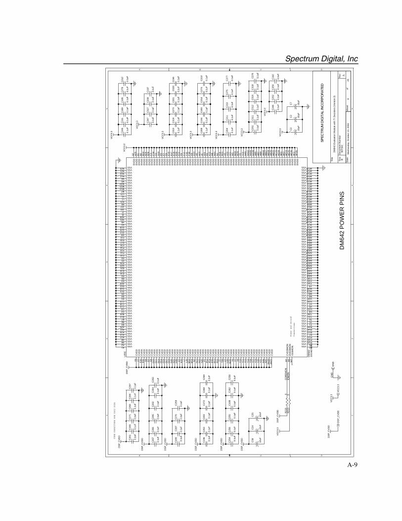
Spectrum Digital, Inc
A-9
1 1
2 2
3 3
4 4
5 5
AA
BB
CC
DD
DM
642
PO
WE
R P
INS
CORECAPACITORS
ARE
0402SIZE
5073
42A
DM
642
Eva
luat
ion
Mod
ule
with
TI D
ecod
ers
(Ver
sion
3)
SPEC
TRU
M D
IGIT
AL IN
CO
RPO
RAT
ED
B
825
Wed
nesd
ay, O
ctob
er 1
3, 2
004
Title
Size
Doc
umen
t Num
ber
Rev
Dat
e:S
heet
of
CO
RE
MO
NIO
MO
N
GN
D
DS
P_C
VD
DV
CC
3.3
GN
D
DS
P_C
VD
D
DS
P_C
VD
D
DS
P_C
VD
D
VC
C3.
3
VC
C3.
3
VC
C3.
3
VC
C3.
3
VC
C3.
3
VC
C3.
3
VC
C3.
3D
SP
_CV
DD
VC
C3.
3
VC
C3.
3
DS
P_C
VDD
DS
P_C
VD
D
DS
P_C
VD
D
DS
P_C
VD
D
VC
C3.
3
VC
C3.
3
DS
P_C
VD
D
C26
4
0.1u
F
C26
3
0.1u
F
C26
8
0.1u
F
C20
3
0.1u
F
C27
2
0.1u
F
C25
3
0.1u
F
C19
6
0.1u
F
C27
5
0.1u
F
+C7
33uFC
214
0.1u
F
C27
8
0.1u
F
+C38
10uF
C20
6
0.1u
F
C31
9
0.1u
F
C20
0
0.1u
F
C26
5
0.1u
F
C19
5
0.1u
F
C21
2
0.1u
F
+C2
33uF
C20
4
0.1u
F
+C3
33uF
C24
7
0.1u
F
C21
0
0.1u
F
C25
8
0.1u
F
C26
9
0.1u
F
C25
9
0.1u
F
C20
5
0.1u
F
C27
0
0.1u
F
C26
7
0.1u
F
C20
2
0.1u
F
C20
9
0.1u
F
C27
4
0.1u
F
C19
7
0.1u
F
C27
3
0.1u
F
C27
1
0.1u
F
C20
8
0.1u
F
C25
7
0.1u
F
C24
9
0.1u
F
C21
1
0.1u
F
C24
6
0.1u
F
C19
4
0.1u
F
C20
1
0.1u
F
C20
7
0.1u
F
C26
0
0.1u
F
+C25
10uF
C19
1
0.1u
F
C21
3
0.1u
F
C19
9
0.1u
F
C27
7
0.1u
F
Power
and
Ground
Connections
U25
C
DM
642
1015
62-0
001
F6 F7 F20
F21
G6
G7
G8
G10
G11
G13
G16
G17
G19
G20
G21
H20 K
7K2
0 L7 L20
N7
P20 T7 T20
U7
U20
W20 Y
6Y
7Y
8Y1
0Y1
1
Y14
Y16
Y17
Y19
Y20
Y21
AA6
AA7
AA20
AA21
A2 A25
B1 B14
B26
E7 E8 E10
E17
E19
E20
F9 F12
F15
F18
G5
G22
H5
H22
J21
K5 K22
M6
M21
N2
P25
R21
U5
U22
V21
W5
W22
Y5 Y22
AA9
AA12
AA15
AA18
AB7
AB8
AB10
AB17
AB19
AB20
AE1
AE13
AE26
AF2
AF25
A1A3A6A8A12A14A19A22A26B3B6B7B13B19C2C4C13C18C23D1D2D5D13D18D22D24E3E6E9E16E18E21E23E26F5F8F10F11F13F14F16F17F19F22G9G12G15G18H1H6
P2P6
P21R7
R20T1T5T6T21T26U6U21V5V7V20V22W1W6W21W26Y9Y12Y15Y18
AB4
AA4AA5AA8AA10AA11AA13AA14AA16AA17AA19AA22AB1AB2
AB6AB9AB18AB21AB26AC3AC5AC18AC22AC24AD2
B2 B25
C3
C24
D4
D23
E5 E22
G14
J6N
20 P7
W25
Y13
AB5
AB22
AC23
AD24
AE2
AE25
M12
M13
M14
M15
N12
N13
N14
N15 P1
2
P13
P14
P15
R12
R13
R14
R15
H21H26J5J7J20J22K6K21L1L6L21M7
M20N5N6
N21N25
AD4AD18AE3AE8AE10AE12AE14AE19AE24AF1AF7AF9AF11AF13AF15AF19AF22AF26
H7
R6
W7
CV
DD
CV
DD
CV
DD
CV
DD
CV
DD
CV
DD
CV
DD
CV
DD
CV
DD
CV
DD
CV
DD
CV
DD
CV
DD
CV
DD
CV
DD
CV
DD
CV
DD
CV
DD
CV
DD
CV
DD
CV
DD
CV
DD
CV
DD
CV
DD
CV
DD
CV
DD
CV
DD
CV
DD
CV
DD
CV
DD
CV
DD
CV
DD
CV
DD
CV
DD
CV
DD
CV
DD
CV
DD
CV
DD
CV
DD
CV
DD
CV
DD
CV
DD
DV
DD
DV
DD
DV
DD
DV
DD
DV
DD
DV
DD
DV
DD
DV
DD
DV
DD
DV
DD
DV
DD
DV
DD
DV
DD
DV
DD
DV
DD
DV
DD
DV
DD
DV
DD
DV
DD
DV
DD
DV
DD
DV
DD
DV
DD
DV
DD
DV
DD
DV
DD
DV
DD
DV
DD
DV
DD
DV
DD
DV
DD
DV
DD
DV
DD
DV
DD
DV
DD
DV
DD
DV
DD
DV
DD
DV
DD
DV
DD
DV
DD
DV
DD
DV
DD
DV
DD
DV
DD
DV
DD
DV
DD
DV
DD
DV
DD
VSSVSSVSSVSSVSSVSSVSSVSSVSSVSSVSSVSSVSSVSSVSSVSSVSSVSSVSSVSSVSSVSSVSSVSSVSSVSSVSSVSSVSSVSSVSSVSSVSSVSSVSSVSSVSSVSSVSSVSSVSSVSSVSSVSSVSSVSSVSSVSSVSSVSS
VSSVSS
VSSVSS
VSSVSSVSSVSSVSSVSSVSSVSSVSSVSSVSSVSSVSSVSSVSSVSSVSSVSSVSSVSS
VSS
VSSVSSVSSVSSVSSVSSVSSVSSVSSVSSVSSVSSVSS
VSSVSSVSSVSSVSSVSSVSSVSSVSSVSSVSS
DV
DD
DV
DD
DV
DD
DV
DD
DV
DD
DV
DD
DV
DD
DV
DD
CVD
D
DV
DD
CVD
DC
VDD
DV
DD
CVD
D
DV
DD
DV
DD
DV
DD
DV
DD
DV
DD
DV
DD
CVD
D
VSS
CV
DD
VSS
VSS
CV
DD
VSS
CV
DD
CV
DD
VSS
CV
DD
VSS
VSS
CV
DD
VSS
CV
DD
VSSVSSVSSVSSVSSVSSVSSVSSVSSVSSVSSVSS
VSSVSSVSS
VSSVSS
VSSVSSVSSVSSVSSVSSVSSVSSVSSVSSVSSVSSVSSVSSVSSVSSVSSVSS
CV
DD
MO
ND
VD
DM
ON
VS
SM
ON
C19
3
0.1u
F
C31
7
0.1u
FC
266
0.1u
F
C32
0
0.1u
F
+C24
10uF
R21
50
R21
30
C31
0
0.1u
F
C26
1
0.1u
F
C31
2
0.1u
F
C31
1
0.1u
F
C31
8
0.1u
F
C25
1
0.1u
F
C27
6
0.1u
F
C31
6
0.1u
F
C25
6
0.1u
F
C19
8
0.1u
F
C25
5
0.1u
F
C26
2
0.1u
F
C25
4
0.1u
F
C25
2
0.1u
F
C19
2
0.1u
F
C25
0
0.1u
F
C24
8
0.1u
F
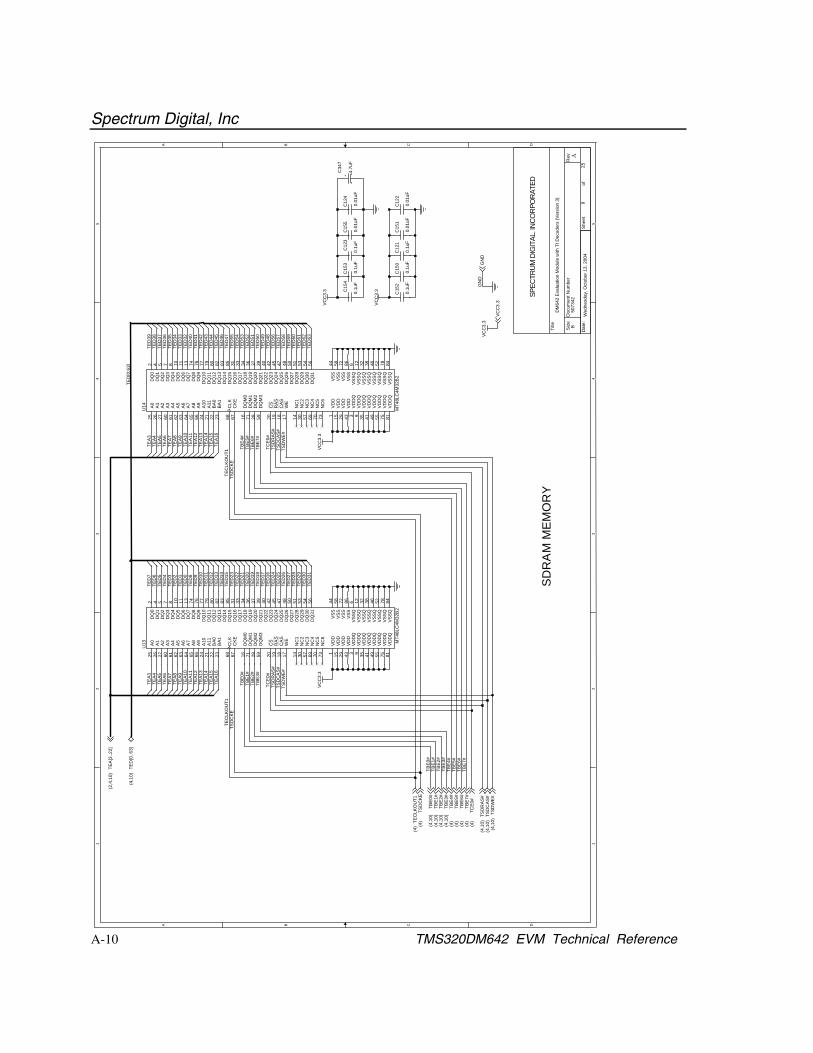
Spectrum Digital, Inc
A-10 TMS320DM642 EVM Technical Reference
1 1
2 2
3 3
4 4
5 5
AA
BB
CC
DD
SD
RA
M M
EM
OR
Y
5073
42A
DM
642
Eva
luat
ion
Mod
ule
with
TI D
ecod
ers
(Ver
sion
3)
SPEC
TRU
M D
IGIT
AL. I
NC
OR
POR
ATED
B
925
Wed
nesd
ay, O
ctob
er 1
3, 2
004
Title
Size
Doc
umen
t Num
ber
Rev
Dat
e:S
heet
of
TSD
CA
S#
TSD
CK
E
TSD
WE
#
TEC
LKO
UT1
TSD
CA
S#
TSD
RA
S#TC
E0#
TED
[0:6
3]
TSD
CKE
TEC
LKO
UT1
TCE
0#TS
DR
AS#
TED
45
TED
40TE
D41
TED
43TE
D42
TED
44
TED
47TE
D46
TSD
WE
#
TEA
8TE
A7
TEA
9
TEA
15
TEA
11TE
A12
TEA
10
TEA
14
TEA
4
TEA
9
TEA
6
TEA
12
TEA
3
TEA
6
TEA
10
TEA
14TE
A13
TEA
15
TEA
11
TEA
7
TEA
5
TEA
16
TEA
3
TEA
16
TEA
8
TEA
4
TEA
13
TEA
5
TED
58
TED
62TE
D63
TED
10
TED
14
TED
26
TED
56
TED
29
TED
13
TED
31
TED
12
TED
9
TED
59
TED
30
TED
60
TED
25
TED
11
TED
28TE
D61
TED
8
TED
57
TED
27
TBE
3#TB
E2#
TBE
7#
TBE
1#
TBE
5#TB
E6#
TBE
4#
TBE
0#
TBE
0#
TBE
1#TB
E2#
TBE
3#
TBE
4#TB
E5#
TBE
6#
TBE
7#
TED
5
TED
1
TED
6
TED
2
TED
0
TED
7
TED
4TE
D3
TED
24
TED
19TE
D20
TED
18
TED
16
TED
15
TED
22TE
D21
TED
17
TED
23
TED
32
TED
38
TED
36
TED
33TE
D34
TED
37
TED
35
TED
39
TED
50TE
D49
TED
48
TED
51
TED
54TE
D55
TED
53TE
D52
GN
D
TEA
[3..2
2](2
,4,1
0)
TED
[0..6
3](4
,10)
TBE2
#(4
,10)
TBE5
#(4
)
TBE7
#(4
)
TBE4
#(4
)
TBE0
#(4
,10)
TBE3
#(4
,10)
TBE6
#(4
)
TBE1
#(4
,10)
TEC
LKO
UT1
(4)
TSD
CA
S#(4
,10)
TSD
WE
#(4
,10)
TSD
RA
S#(4
,10)
TCE
0#(4
)
TSD
CKE
(4)
VC
C3.
3
GN
D
VC
C3.
3V
CC
3.3
VC
C3.
3
VC
C3.
3
VCC
3.3
U13 M
T48L
C4M
32B
2
2 4 5 7 8 10 11 13
22 232425 26 27
45 47 48 50 51 53 54 56
68
77
60 61 62 63 64 65 6674 76 79 80 82 83 85 31 33 34 36 37 39 40 42 44 58 72 86 126 32 38 46 52 78 84
1 15 29 43 3 9 35 41 49 55 75 811867 19 172016 71 28 5921 14 30 57 69 70 73
DQ
0D
Q1
DQ
2D
Q3
DQ
4D
Q5
DQ
6D
Q7
BA
0B
A1
A10
A0
A1
A2
DQ
24D
Q25
DQ
26D
Q27
DQ
28D
Q29
DQ
30D
Q31
CLK
DQ
10
A3
A4
A5
A6
A7
A8
A9
DQ
8D
Q9
DQ
11D
Q12
DQ
13D
Q14
DQ
15D
Q16
DQ
17D
Q18
DQ
19D
Q20
DQ
21D
Q22
DQ
23
VSS
VSS
VSS
VSS
VSS
QV
SSQ
VSS
QV
SSQ
VSS
QV
SSQ
VSS
QV
SSQ
VD
DV
DD
VD
DV
DD
VD
DQ
VD
DQ
VD
DQ
VD
DQ
VD
DQ
VD
DQ
VD
DQ
VD
DQ
CA
S
CK
E
RA
S
WE
CS
DQ
M0
DQ
M1
DQ
M2
DQ
M3
A11
NC
1N
C2
NC
3N
C4
NC
5N
C6
C15
3
0.1u
F
+C
347
4.7u
F
C15
2
0.1u
F
C12
3
0.1u
F
C15
1
0.01
uF
C15
0
0.1u
F
C15
5
0.01
uF
C12
2
0.01
uF
C12
1
0.1u
F
C12
4
0.01
uF
C15
4
0.1u
F
U14
MT4
8LC
4M32
B2
2 4 5 7 8 10 11 13
22 232425 26 27
45 47 48 50 51 53 54 56
68
77
60 61 62 63 64 65 6674 76 79 80 82 83 85 31 33 34 36 37 39 40 42 44 58 72 86 126 32 38 46 52 78 84
1 15 29 43 3 9 35 41 49 55 75 811867 19 172016 71 28 5921 14 30 57 69 70 73
DQ
0D
Q1
DQ
2D
Q3
DQ
4D
Q5
DQ
6D
Q7
BA0
BA1
A10
A0
A1
A2
DQ
24D
Q25
DQ
26D
Q27
DQ
28D
Q29
DQ
30D
Q31
CLK
DQ
10
A3
A4
A5
A6
A7
A8
A9
DQ
8D
Q9
DQ
11D
Q12
DQ
13D
Q14
DQ
15D
Q16
DQ
17D
Q18
DQ
19D
Q20
DQ
21D
Q22
DQ
23
VSS
VSS
VSS
VSS
VSS
QVS
SQ
VSS
QVS
SQ
VSS
QVS
SQ
VSS
QVS
SQ
VD
DV
DD
VD
DV
DD
VD
DQ
VD
DQ
VD
DQ
VD
DQ
VD
DQ
VD
DQ
VD
DQ
VD
DQ
CA
S
CK
E
RA
S
WE
CS
DQ
M0
DQ
M1
DQ
M2
DQ
M3
A11
NC
1N
C2
NC
3N
C4
NC
5N
C6
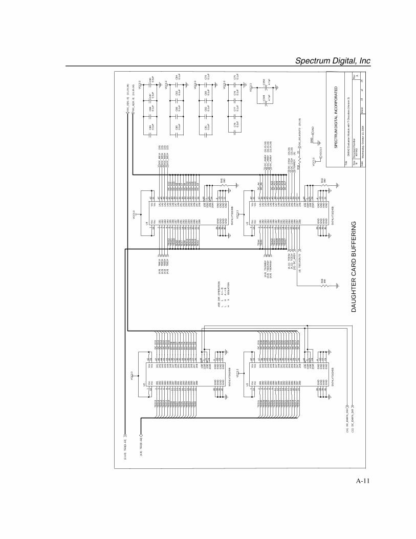
Spectrum Digital, Inc
A-11
#OE
DIR
OP
ERA
TIO
NL
L
A
<-- B
L
H
A --
> B
H
X
ISO
LATI
ON
DA
UG
HTE
R C
AR
D B
UFF
ER
ING
5073
42A
DM
642
Eva
luat
ion
Mod
ule
with
TI D
ecod
ers
(Ver
sion
3)
SPEC
TRU
M D
IGIT
AL. I
NC
OR
POR
ATED
B
1025
Wed
nesd
ay, O
ctob
er 1
3, 2
004
Title
Siz
eD
ocum
ent N
umbe
rR
ev
Dat
e:S
heet
of
TED
30
TED
26
TED
29
TED
16
TED
31
TED
23
TED
28TE
D27
TED
25TE
D24
TED
22TE
D21
TED
20TE
D19
TED
18TE
D17
GN
D
TED
12
TED
1
TED
10
TED
14
TED
8
TED
0
TED
15
TED
2TE
D3
TED
4TE
D5
TED
6TE
D7
TED
9
TED
11
TED
13
DC
_D9
DC
_D8
DC
_D4
DC
_D13
DC
_D3
DC
_D15
DC
_D12
DC
_D6
DC
_D1
DC
_D5
DC
_D0
DC
_D11
DC
_D7
DC
_D14
DC
_D2
DC
_D10
DC
_D25
DC
_D16
DC
_D29
DC
_D21
DC
_D30
DC
_D19
DC
_D23
DC
_D31
DC
_D22
DC
_D17
DC
_D20
DC
_D24
DC
_D27
DC
_D18
DC
_D28
DC
_D26
TEA
9
TEA
4
TEA
12
TEA
14
TEA
10
TEA
6
TEA
11
TEA
7
TEA
5
DC
_A11
DC
_A6
DC
_A4
DC
_A3
DC
_A5
DC
_A17
DC
_A12
DC
_A13
DC
_A18
TEA
8
TEA
15TE
A16
TEA
3TE
A13
TEA
18TE
A17
TEA
19TE
A20
TEA
22TE
A21
DC
_A19
DC
_A20
DC
_A21
DC
_A22
DC
_A16
DC
_A15
DC
_A14
DC
_A7
DC
_A8
DC
_A9
DC
_A10
DC
_A[2
2..3
](1
1,15
,16)
TEA
[3..2
2](2
,4,9
)D
C_D
[31.
.0]
(11,
15,1
6)
TEC
LKO
UT2
(4)
DC
_AR
DY
(15)
DC
_EC
LKO
UT2
(15,
16)
DC
_EM
IFA
_DIR
(11)
DC
_EM
IFA
_OE
#(1
1)
TED
[0..6
3](4
,9)
TEA
RD
Y(4
)
VCC
3.3
GN
D
TBE3
#(4
,9)
TBE0
#(4
,9)
TBE1
#(4
,9)
TBE2
#(4
,9)
DC
_BE
3#(1
5)
DC
_BE
2#(1
5)
DC
_BE
1#(1
5)
DC
_BE
0#(1
5)
TSD
WE
#(4
,9) TS
DC
AS
#(4
,9)
TSD
RA
S#
(4,9
)D
C_A
RE
#(1
1,15
,16)
DC
_AO
E#
(11,
15,1
6)
DC
_AW
E#
(11,
15,1
6)
DC
_CE
2#(1
5,16
)D
C_C
E3#
(15,
16)
TCE
3#(4
,11)
TCE
2#(4
,11)
VC
C3.
3
VCC
3.3
VC
C3.
3
VC
C3.
3
VC
C3.
3
VC
C3.
3
VC
C3.
3
VC
C3.
3
VC
C3.
3
VC
C3.
3
R39
360
R43
360
U3
SN
74LV
T162
45B
7 183142 47 46 44 43 41 40 38 37
2 3 5 6 8 9 11 1236 35 33 32 30 29 27 26
13 14 16 17 19 20 22 23
48 1 25 24 4 10 15 21
28 34 39 45
Vcc
Vcc
Vcc
Vcc
1A1
1A2
1A3
1A4
1A5
1A6
1A7
1A8
1B1
1B2
1B3
1B4
1B5
1B6
1B7
1B8
2A1
2A2
2A3
2A4
2A5
2A6
2A7
2A8
2B1
2B2
2B3
2B4
2B5
2B6
2B7
2B8
1OE
1DIR
2OE
2DIR
GN
DG
ND
GN
DG
ND
GN
DG
ND
GN
DG
ND
U4
SN
74LV
T162
45B
7 183142 47 46 44 43 41 40 38 37
2 3 5 6 8 9 11 1236 35 33 32 30 29 27 26
13 14 16 17 19 20 22 23
48 1 25 24 4 10 15 21
28 34 39 45
Vcc
Vcc
Vcc
Vcc
1A1
1A2
1A3
1A4
1A5
1A6
1A7
1A8
1B1
1B2
1B3
1B4
1B5
1B6
1B7
1B8
2A1
2A2
2A3
2A4
2A5
2A6
2A7
2A8
2B1
2B2
2B3
2B4
2B5
2B6
2B7
2B8
1OE
1DIR
2OE
2DIR
GN
DG
ND
GN
DG
ND
GN
DG
ND
GN
DG
ND
R38
33
C88
0.1u
FC
890.
1uF
C87
0.1u
FC
900.
1uF
U2
SN
74LV
T162
45B
7 183142 47 46 44 43 41 40 38 37
2 3 5 6 8 9 11 1236 35 33 32 30 29 27 26
13 14 16 17 19 20 22 23
48 1 25 24 4 10 15 21
28 34 39 45
Vcc
Vcc
Vcc
Vcc
1A1
1A2
1A3
1A4
1A5
1A6
1A7
1A8
1B1
1B2
1B3
1B4
1B5
1B6
1B7
1B8
2A1
2A2
2A3
2A4
2A5
2A6
2A7
2A8
2B1
2B2
2B3
2B4
2B5
2B6
2B7
2B8
1OE
1DIR
2OE
2DIR
GN
DG
ND
GN
DG
ND
GN
DG
ND
GN
DG
ND
U5
SN
74LV
T162
45B
7 183142 47 46 44 43 41 40 38 37
2 3 5 6 8 9 11 1236 35 33 32 30 29 27 26
13 14 16 17 19 20 22 23
48 1 25 24 4 10 15 21
28 34 39 45
Vcc
Vcc
Vcc
Vcc
1A1
1A2
1A3
1A4
1A5
1A6
1A7
1A8
1B1
1B2
1B3
1B4
1B5
1B6
1B7
1B8
2A1
2A2
2A3
2A4
2A5
2A6
2A7
2A8
2B1
2B2
2B3
2B4
2B5
2B6
2B7
2B8
1OE
1DIR
2OE
2DIR
GN
DG
ND
GN
DG
ND
GN
DG
ND
GN
DG
ND
R45
360
C79
0.1u
FC
800.
1uF
C85
0.1u
FC
860.
1uF
C83
0.1u
FC
840.
1uF
C78
0.1u
FC
750.
1uF
C76
0.1u
FC
770.
1uF
C82
0.1u
FC
810.
1uF
+C
350
4.7u
F
+C
349
4.7u
F
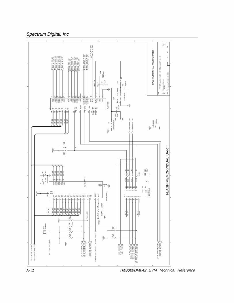
Spectrum Digital, Inc
A-12 TMS320DM642 EVM Technical Reference
5 5
4 4
3 3
2 2
1 1
DD
CC
BB
AA
FLA
SH M
EM
OR
Y/D
UA
L U
AR
T50
7342
A
DM
642
Eva
luat
ion
Mod
ule
with
TI D
ecod
ers
(Ver
sion
3)
SPEC
TRU
M D
IGIT
AL. I
NC
OR
POR
ATED
B
1125
Wed
nesd
ay, O
ctob
er 1
3, 2
004
Title
Size
Doc
umen
t Num
ber
Rev
Dat
e:S
heet
of
DC
_D0
DC
_D1
DC
_D2
DC
_D3
DC
_D4
DC
_D5
DC
_D6
DC
_D7
DC
_D0
DC
_D1
DC
_D2
DC
_D3
DC
_D4
DC
_D5
DC
_D6
DC
_D7
DC
_A3
DC
_A4
DC
_A5
DC
_A22
DC
_A21
DC
_A14
DC
_A5
DC
_A9
DC
_A11
DC
_A16
DC
_A15
DC
_A13
DC
_A3
DC
_A6
DC
_A18
DC
_A20
DC
_A4
DC
_A7
DC
_A8
DC
_A10
DC
_A12
DC
_A17
DC
_A19
FLAS
H_C
E#
DC
_A22
GN
D
UA
RT_
CLK
DC
_A8
DC
_A7
DC
_A6
SYS
TEM
_RE
SET#
(3,1
4,16
,17,
18,1
9,20
,21,
25)
FLA
SH
_EXT
_A20
(16)
FLA
SH
_EXT
_A21
(16)
DC
_D[3
1..0
](1
0,15
,16)
DC
_A[2
2..3
](1
0,15
,16)
DC
_AW
E#(1
0,15
,16)
DC
_AR
E#
(10,
15,1
6)U
AR
T_IN
TA(1
6)U
AR
T_IN
TB(1
6)
SY
STE
M_R
ES
ET
(20,
25)
UA
RT_
B_D
CD
(12)
UA
RT_
B_R
I(1
2)
UA
RT_
A_R
I(1
2)
TCE
1#(4
,16)
FLA
SH
_EXT
_A19
(16)
DC
_AO
E#
(10,
15,1
6)
DC
_AW
E#(1
0,15
,16)
DC
_AR
E#
(10,
15,1
6)
UA
RT_
A_R
X(1
2)U
AR
T_A
_TX
(12)
UA
RT_
A_D
TR(1
2)U
AR
T_A
_RTS
(12)
UA
RT_
B_R
TS(1
2)
UA
RT_
B_R
X(1
2)
UA
RT_
B_D
TR(1
2)
UA
RT_
B_C
TS(1
2)
UA
RT_
B_T
X(1
2)
UA
RT_
B_D
SR
(12)
UA
RT_
RX
DY_
A#
(16)
UA
RT_
TXD
Y_A
#(1
6)U
AR
T_R
XD
Y_B
#(1
6)U
AR
T_TX
DY
_B#
(16)
UA
RT_
A_D
CD
(12)
UA
RT_
A_D
SR
(12)
UA
RT_
A_C
TS(1
2)
DC
_AW
E#(1
0,15
,16)
DC
_AR
E#
(10,
15,1
6)
DC
_EM
IFA
_OE
#(1
0)
DC
_EM
IFA
_DIR
(10)
VC
C3.
3
GN
D
FPG
A_D
C_E
MIF
_DIR
(16)
FPG
A_D
C_E
MIF
_OE
#(1
6)
TCE
2#(4
,10)
TCE
3#(4
,10)
TSO
E3#
(4,1
6)
FLA
SH
_EX
T_A2
2(1
6)
VCC
3.3
VC
C3.
3
VC
C3.
3V
CC
3.3
VCC
3.3
VC
C3.
3
VC
C3.
3
VC
C3.
3
VCC
3.3
C71
NO
PO
P
C73
0.1u
FC
72.0
01uF
L1
BLM
21P
221S
N
R36
33
U9 TL
16C
752B
44 45 46 47 48 1 2 3 28 27 26 2410 11 369
19 15
45 7 40 8 16 23 2038 39 21
12
13 1431 2922 30 42 1743 18 634 354133 32
25 37
D0
D1
D2
D3
D4
D5
D6
D7
A0
A1
A2
NC
1
CSA
CSB
RES
ET
OP
B
IOR
D
IOW
R
RX
B
RX
ATX
AC
DA
TXB
CD
BC
TSB
DSR
B
CTS
AD
SRA
RIB
NC
0
XTA
L1X
TAL2
RX
RD
YA
INTB
RTS
B
INTA
VC
C
GN
D
TXR
DYA
RX
RD
YB
TXR
DYB
DTR
A
DTR
B
RIA
RTS
A
OP
A
NC
2N
C3
R8
10K
C12
00.
1uF
R24
233
R24
333
C54
0.1u
F
R69
10K
TP30
Test
Poi
nt
1
C55
0.1u
F
R71
10K
R70
33R
6833
U15 G
AL1
6LV8
-310
0710
-000
3
1 2 3 4 5 6 7 8 9 11
12 13 14 15 16 17 18 19 20 10
I0 I1 I2 I3 I4 I5 I6 I7 I8 I9
F0 F1 F2 F3 F4 F5 F6 F7
VC
C
GN
D
R72
33
R9
10K
U10
29.4
912
MH
z
4 321
VCC
OU
TG
ND
EN
U6
AM29
LV03
3C
21 20 19 18 17 16 15 14 8 7 36 6 5 4 3 2 1 40 13 29
25 26 27 28 32 33 34 35
31
1138 22 24 9
12
1037
30
2339
A0
A1
A2
A3
A4
A5
A6
A7
A8
A9
A10
A11
A12
A13
A14
A15
A16
A17
A18
A21
DQ
0D
Q1
DQ
2D
Q3
DQ
4D
Q5
DQ
6D
Q7
VCC2
AC
C
A20
CE
OE
WE
RD
Y-B
Y
RE
SE
T
A19
VCC
VSS1VSS2
R12
10K
R13
NO
PO
P+
C35
1
10uF
R10
10K
R11
10K
R64
10K
R65
10K
C74
0.1u
F
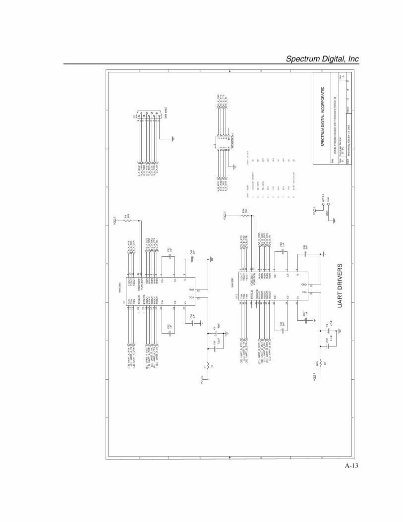
Spectrum Digital, Inc
A-13
5 5
4 4
3 3
2 2
1 1
DD
CC
BB
AA
UART
1 2 3 4 5 6 7 8 9
NAME
CARRIER
DETECT
OUT
OUT
OUT
DTR
GND
RTS
CTS
TX
DATA
IN
IN
IN
IN
IN
RING
INDICATOR
GND
DSR
RX
DATA
UARTIN/OUT
UA
RT
DR
IVE
RS
5073
42A
DM
642
Eva
luat
ion
Mod
ule
with
TI D
ecod
ers
(Ver
sion
3)
SPEC
TRU
M D
IGIT
AL. I
NC
OR
POR
ATED
B
1225
Wed
nesd
ay, O
ctob
er 1
3, 2
004
Title
Size
Doc
umen
t Num
ber
Rev
Dat
e:S
heet
of
GN
D
S_A
_RTS
S_A
_RX
D
S_A
_CTS
S_A
_RI
S_A
_DC
D
S_A
_DTR
S_A
_DS
R
S_A
_TX
D
S_A
_TX
D
S_A
_DS
RS
_A_D
CD
S_A
_RTS
S_A
_RI
S_A
_CTS
S_A
_RX
D
S_A
_DTR
UA
RT_
A_D
SR
(11)
UAR
T_A
_DC
D(1
1)
UA
RT_
A_D
TR(1
1)
UA
RT_
A_C
TS(1
1)
UA
RT_
A_T
X(1
1)
UA
RT_
A_R
I(1
1)UA
RT_
A_R
TS(1
1)
UA
RT_
A_R
X(1
1)
S_B
_TX
D
S_B
_DS
RS
_B_D
CD
S_B
_RTS
S_B
_RI
S_B
_CTS
S_B
_RX
D
S_B
_DTR
UA
RT_
B_D
SR
(11)
UAR
T_B
_DC
D(1
1)
UA
RT_
B_D
TR(1
1)
UA
RT_
B_C
TS(1
1)U
AR
T_B
_RI
(11)U
AR
T_B
_RTS
(11)
UA
RT_
B_R
X(1
1)
S_B
_RTS
S_B
_RX
DS
_B_C
TSS
_B_R
I
S_B
_DC
D
S_B
_DTR
S_B
_DSR
S_B
_TX
D
GN
D
VC
C3.
3
UA
RT_
B_T
X(1
1)
VC
C3.
3
VC
C3.
3
VC
C3.
3
VCC
3.3
VC
C3.
3
+C
6 47uF
C53 0.
1uF
J12
HE
AD
ER
5X
2
12
34
56
78
910
J11
DB
9 M
ALE
594837261
R7 10
R6
10K
+C
521u
F
+C
501u
F
+C
511u
F
+
C66
1uF
+C
681u
F
R34
10K
R35 10
C70 0.
1uF
+C
9 47uF
+C
67 1uF
U11
MA
X32
43
14 13 12 151621 20 19 18 17 28 24 27
26
25
3214 5 623229 10 11 7 8
T1IN
T2IN
T3IN
R5O
UT
R4O
UT
INV
ALI
D
R2O
UTB
R1O
UT
R2O
UT
R3O
UT
C1+
C1-
V+
VCC
GND
V-
C2-
C2+
R1I
NR
2IN
R3I
N
FOR
CEO
NFO
RC
EOFF
T1O
UT
T2O
UT
T3O
UT
R4I
NR
5IN
+
C49
1uF
+C
691u
F
U7
MA
X324
3
14 13 12 151621 20 19 18 17 28 24 27
26
25
3214 5 623229 10 11 7 8
T1IN
T2IN
T3IN
R5O
UT
R4O
UT
INV
ALI
D
R2O
UTB
R1O
UT
R2O
UT
R3O
UT
C1+
C1-
V+
VCC
GND
V-
C2-
C2+
R1I
NR
2IN
R3I
N
FOR
CE
ON
FOR
CEO
FF
T1O
UT
T2O
UT
T3O
UT
R4I
NR
5IN
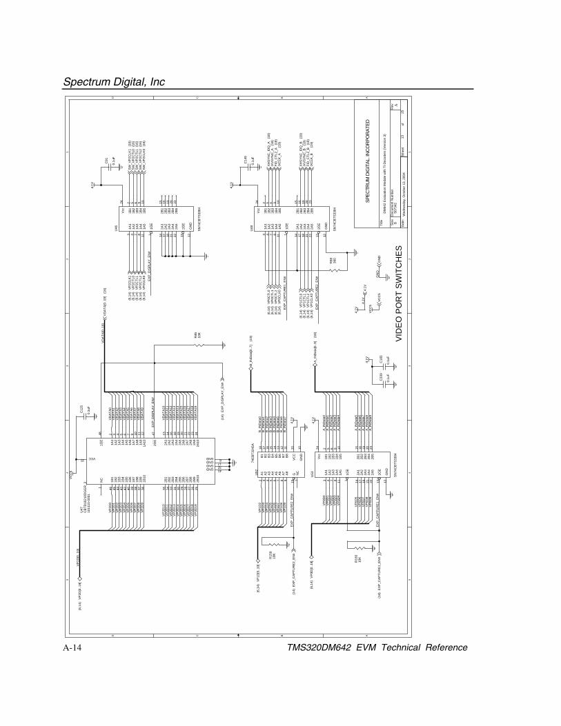
Spectrum Digital, Inc
A-14 TMS320DM642 EVM Technical Reference
5 5
4 4
3 3
2 2
1 1
DD
CC
BB
AA
VID
EO
PO
RT
SW
ITC
HE
S50
7342
A
DM
642
Eva
luat
ion
Mod
ule
with
TI D
ecod
ers
(Ver
sion
3)
SPEC
TRU
M D
IGIT
AL. I
NC
OR
POR
ATED
B
1325
Wed
nesd
ay, O
ctob
er 1
3, 2
004
Title
Size
Doc
umen
t Num
ber
Rev
Dat
e:S
heet
of
VD
ATA
9
VP2
D2
VD
ATA
10
VD
ATA
15V
DA
TA16
VD
ATA
14V
DA
TA13
VD
ATA
8
VP2
D4
VD
ATA
1
VD
ATA
5
VP2
D0
VP
2D19
VP
2D14
VP
2D12
VP2
D8
VD
ATA
17
VD
ATA
4
VP2
D6
VD
ATA
19
VP2
D1
VD
ATA
12V
DA
TA11
VD
ATA
6
VP
2D15
VD
ATA
18
VP
2D11
VP2
D9
VD
ATA7
VP
2D18
VP2
D7
VP2
D3
VD
ATA
[0..1
9]
VP
2D[0
..19]
VD
ATA2
VP
2D17
VP2
D5
VP
2D10
VP
2D16
VP
2D13
VD
ATA0
VD
ATA3
4.1V
EX
P_D
ISP
LAY
_EN
#
EXP
_CA
PTU
RE2
_EN
#
EXP
_CA
PTU
RE1
_EN
# GN
D
B_I
ND
ata6
B_I
ND
ata7
B_I
ND
ata2
B_I
ND
ata5
B_I
ND
ata3
B_I
ND
ata0
B_I
ND
ata1
B_I
ND
ata4
VP1
D2
VP1
D3
VP1
D4
VP1
D5
VP1
D6
VP1
D7
VP1
D8
VP1
D9
EX
P_D
ISPL
AY
_EN
#
EXP
_CA
PTU
RE
2_E
N#
A_I
ND
ata4
A_I
ND
ata9
A_I
ND
ata8
A_I
ND
ata7
A_I
ND
ata6
A_I
ND
ata5
EXP
_CA
PTU
RE
1_E
N#
VP
0D4
VP
0D3
VP0D
9VP
0D8
VP0D
7VP
0D6
VP0D
5
VP
0D2
VP
0D1
VP
0D0
A_I
ND
ata0
A_I
ND
ata2
A_I
ND
ata1
A_I
ND
ata3
XH
SY
NC
_ID
Q_A
(18)
XH
SY
NC
_ID
Q_B
(19)
IXVS
YN
C_A
(18)
IXVS
YN
C_B
(19)
VP
2D[0
..19]
(6,1
4)
VD
ATA
[0..1
9](1
6)
VP
0D[0
..19]
(6,1
4)
VP
0CTL
2(6
,14)
VP
0CTL
1(6
,14)
VP
0CLK
0(6
,14)
VP
0CTL
0(6
,14) VP
1CLK
0(6
,14)
VP1C
TL1
(6,1
4)VP
1CTL
2(6
,14)
VP1C
TL0
(6,1
4)
VP
2CTL
2(6
,14)
VP
2CLK
0(6
,14)
VP
2CLK
1(6
,14)
VP
2CTL
0(6
,14)
VP
2CTL
1(6
,14)
4.1V
SW_V
P2C
TL2
(16)
SW_V
P2C
LK0
(16)
SW_V
P2C
LK1
(16)
SW_V
P2C
TL0
(16)
SW_V
P2C
TL1
(16)
IXC
LK_A
(18)
IXC
LK_B
(19)
GN
D
VC
C5
B_I
ND
ata[
0..7
](1
9)
VP1D
[0..1
9](6
,14)
EX
P_D
ISP
LAY_
EN
#(1
4)
EX
P_C
APTU
RE
1_E
N#
(14)
EXP
_CA
PTU
RE2
_EN
#(1
4)
FID
_CTL
2_B
(19)
FID
_CTL
2_A
(18)
A_I
ND
ata[
0..9
](1
8)
VC
C5
4.1V
4.1V
4.1V
VC
C5
4.1V
4.1V
4.1V
U48
SN
74C
BTS
3384
1 133 4 7 8 11
2 5 6 9 10
14 17 18 21 22
24
12
15 16 19 20 23
1OE
2OE
1A1
1A2
1A3
1A4
1A5
1B1
1B2
1B3
1B4
1B5
2A1
2A2
2A3
2A4
2A5
Vcc
GN
D
2B1
2B2
2B3
2B4
2B5
U52
74C
BT3
245A
218
317
416
515
614
713
812
911
19 120 10
A1
B1
A2
B2
A3
B3
A4
B4
A5
B5
A6
B6
A7
B7
A8
B8
G NC
VC
C
GN
D
C12
5
0.1u
F
C18
3
0.1u
F
U46
SN
74C
BTS
3384
1 133 4 7 8 11
2 5 6 9 10
14 17 18 21 22
24
12
15 16 19 20 23
1OE
2OE
1A1
1A2
1A3
1A4
1A5
1B1
1B2
1B3
1B4
1B5
2A1
2A2
2A3
2A4
2A5
Vcc
GN
D
2B1
2B2
2B3
2B4
2B5
R46
10K
R88 360
U53
SN
74C
BTS
3384
1 133 4 7 8 11
2 5 6 9 10
14 17 18 21 22
24
12
15 16 19 20 23
1OE
2OE
1A1
1A2
1A3
1A4
1A5
1B1
1B2
1B3
1B4
1B5
2A1
2A2
2A3
2A4
2A5
Vcc
GN
D
2B1
2B2
2B3
2B4
2B5
R15
910
K
C14
9
0.1u
F
C33
9
0.1u
F
R16
010
K
C91
0.1u
F
U47
CB
TD16
210D
GG
R_3
1011
15-0
001
4748 2 13
46 35
8173241
15
3 4 5 6 7 9 10 11 12 14 16 18 19 20 21 22 23 24
1 45 44 43 42 40 39 38 37 36 34 33 31 30 29 28 27 26 25
2OE
1OE
1A1
2A1
1B1
2B1
GNDGNDGNDGND
VCC
1A2
1A3
1A4
1A5
1A6
1A7
1A8
1A9
1A10
2A2
2A3
2A4
2A5
2A6
2A7
2A8
2A9
2A10
NC
1B2
1B3
1B4
1B5
1B6
1B7
1B8
1B9
1B10
2B2
2B3
2B4
2B5
2B6
2B7
2B8
2B9
2B10
Spectrum Digital, Inc
A-15
5 5
4 4
3 3
2 2
1 1
DD
CC
BB
AA
VID
EO
PO
RTS
DA
UG
HTE
R C
AR
D C
ON
NE
CTI
ON
S50
7342
A
DM
642
Eva
luat
ion
Mod
ule
with
TI D
ecod
ers
(Ver
sion
3)
SPEC
TRU
M D
IGIT
AL. I
NC
OR
POR
ATED
B
1425
Wed
nesd
ay, O
ctob
er 1
3, 2
004
Title
Size
Doc
umen
t Num
ber
Rev
Dat
e:S
heet
of
VP
2D18
VP
2D16
VP
2D14
VP
2D19
VP
2D17
VP
2D15
VP
2D12
VP
2D10
VP
2D13
VP
2D11
VP
2D8
VP
2D6
VP
2D4
VP
2D9
VP
2D7
VP
2D5
VP
2D2
VP
2D0
VP
2D3
VP
2D1
VP
1D0
VP
1D3
GN
D
VP
0D7
VP
1D5
VP
1D9
VP
0D5
VP
1D10
VP
1D2
VP
0D11
VP
1D11
VP
0D14
VP
1D7
VP
0D10
VP
0D16
VP
1D6
VP
1D12
VP
0D15
VP
0D6
VP
0D1
VP
0D8
VP
0D12
VP
1D1
VP
0D18
VP
0D17
VP
0D3
VP
0D0
VP
0D4
VP
0D13
VP
1D13
VP1D
14
VP
0D19
VP
0D2
VP
1D4
VP1
D16
VP
1D19
VP
1D8
VP1
D18
VP
1D15
VP
1D17
VP
0D9
VP2C
LK0
(6,1
3)
VP
2CLK
1(6
,13)
VP2C
TL0
(6,1
3)VP
2CTL
2(6
,13)
VP
1CTL
1(6
,13)
VP
1CTL
0(6
,13)
VP
1D[0
:19]
(6,1
3)
VP
0D[0
:19]
(6,1
3)
DSP
_SC
L0(3
,18,
19,2
0,23
)
DS
P_T
INP
0(3
) DS
P_T
OU
T0(3
,7)
DS
P_T
OU
T1(2
,3)
DS
P_T
INP1
(3)
DS
P_G
PIO
_3(2
,3)
DS
P_E
XTI
NT5
(3)
DS
P_E
XTI
NT4
(3)
DS
P_N
MI
(3)
SYS
TEM
_RE
SET#
(3,1
1,16
,17,
18,1
9,20
,21,
25)
EX
P_C
AP
TUR
E1_
EN
#(1
3)E
XP_
CA
PTU
RE
2_E
N#
(13)
VP
0CTL
0(6
,13)
VP
0CLK
1(6
)
EXP
_DIS
PLA
Y_E
N#
(13)
US
ER
_GP
IO_0
(16)
US
ER
_GPI
O_1
(16)
US
ER
_GP
IO_2
(16)
US
ER
_GP
IO_4
(16)
US
ER
_GPI
O_5
(16)
US
ER
_GPI
O_6
(16)
US
ER
_GPI
O_7
(16)
DC
AR
D_S
TCLK
(6)
DSP
_SD
A0
(3,1
8,19
,20,
23)
US
ER
_GPI
O_3
(16)
VP2C
TL1
(6,1
3)
VC
C3.
3
GN
D
VP
2D[0
:19]
(6,1
3)
VCC
5
VP
1CLK
1(6
)
VP
0CTL
2(6
,13)
EXP
_AU
DIO
_EN
#(2
,6)
VP
1CLK
0(6
,13)
VP
0CLK
0(6
,13)
VP
0CTL
1(6
,13)
VP
1CTL
2(6
,13)
VC
C5
VC
C3.
3
VC
C5
VC
C3.
3
VC
C3.
3V
CC
5
DC
_P2
CO
NN
ECTO
R 4
5 X
2
12
34
56
78
910
1112
1314
1516
1718
1920
2122
2324
2526
2728
2930
3132
3334
3536
3738
3940
4142
4344
4546
4748
4950
5152
5354
5556
5758
5960
6162
6364
6566
6768
6970
7172
7374
7576
7778
7980 9088868482
81 83 85 87 89
12
34
56
78
910
1112
1314
1516
1718
1920
2122
2324
2526
2728
2930
3132
3334
3536
3738
3940
4142
4344
4546
4748
4950
5152
5354
5556
5758
5960
6162
6364
6566
6768
6970
7172
7374
7576
7778
7980 9088868482
81 83 85 87 89
DC
_P1
CO
NN
EC
TOR
45
X 2
12
34
56
78
910
1112
1314
1516
1718
1920
2122
2324
2526
2728
2930
3132
3334
3536
3738
3940
4142
4344
4546
4748
4950
5152
5354
5556
5758
5960
6162
6364
6566
6768
6970
7172
7374
7576
7778
7980 9088868482
81 83 85 87 89
12
34
56
78
910
1112
1314
1516
1718
1920
2122
2324
2526
2728
2930
3132
3334
3536
3738
3940
4142
4344
4546
4748
4950
5152
5354
5556
5758
5960
6162
6364
6566
6768
6970
7172
7374
7576
7778
7980 9088868482
81 83 85 87 89
Spectrum Digital, Inc
A-16 TMS320DM642 EVM Technical Reference
5 5
4 4
3 3
2 2
1 1
DD
CC
BB
AA
EXTE
RN
AL
MEM
OR
Y IN
TER
FAC
ED
AU
GH
TER
CA
RD
CO
NN
EC
TIO
NS
5073
42A
DM
642
Eva
luat
ion
Mod
ule
with
TI D
ecod
ers
(Ver
sion
3)
SPEC
TRU
M D
IGIT
AL. I
NC
OR
POR
ATED
B
1525
Wed
nesd
ay, O
ctob
er 1
3, 2
004
Title
Size
Doc
umen
t Num
ber
Rev
Dat
e:S
heet
of
DC
_D9
DC
_D8
DC
_D4
DC
_D13
DC
_D3
DC
_D15
DC
_D12
DC
_D6
DC
_D1
DC
_D5
DC
_D0
DC
_D11
DC
_D7
DC
_D14
DC
_D2
DC
_D10
DC
_D29
DC
_D28
DC
_D18
DC
_D17
DC
_D24
DC
_D27
DC
_D31
DC
_D22
DC
_D19
DC
_D23
DC
_D21
DC
_D20
DC
_D30
DC
_D26
DC
_D16
DC
_D25
DC
_A20
DC
_A19
DC
_A22
DC
_A21
DC
_A15
DC
_A7
DC
_A8
DC
_A10
DC
_A3
DC
_A6
DC
_A9
DC
_A14
DC
_A5
DC
_A18
DC
_A11
DC
_A16
DC
_A17
DC
_A12
DC
_A13
DC
_A4
GN
D
DC
_A[2
2..3
](1
0,11
,16)
DC
_D[3
1..0
](1
0,11
,16)
DC
_BE2
#(1
0)D
C_B
E3#
(10)
DC
_BE0
#(1
0)D
C_B
E1#
(10)
DC
_EC
LKO
UT2
(10,
16)
DC
_CE
2#(1
0,16
)D
C_C
E3#
(10,
16)
DC
_AO
E#(1
0,11
,16)
DC
_AR
E#
(10,
11,1
6)D
C_A
WE
#(1
0,11
,16)
DC
_AR
DY
(10)
VC
C3.
3
GN
D
VCC
3.3
VC
C3.
3
R24
14.
7K
DC
_P3
CO
NN
EC
TOR
45
X 2
12
34
56
78
910
1112
1314
1516
1718
1920
2122
2324
2526
2728
2930
3132
3334
3536
3738
3940
4142
4344
4546
4748
4950
5152
5354
5556
5758
5960
6162
6364
6566
6768
6970
7172
7374
7576
7778
7980 9088868482
81 83 85 87 89
12
34
56
78
910
1112
1314
1516
1718
1920
2122
2324
2526
2728
2930
3132
3334
3536
3738
3940
4142
4344
4546
4748
4950
5152
5354
5556
5758
5960
6162
6364
6566
6768
6970
7172
7374
7576
7778
7980 9088868482
81 83 85 87 89
Spectrum Digital, Inc
A-17
2 2
1 1
BB
AA
5073
42B
DM
642
Eva
luat
ion
Mod
ule
with
TI D
ecod
ers
(Ver
sion
3)
SPEC
TRU
M D
IGIT
AL. I
NC
OR
POR
ATED
B
1625
Wed
nesd
ay, O
ctob
er 1
3, 2
004
Title
Size
Doc
umen
t Num
ber
Rev
Dat
e:S
heet
of
VDATA17VDATA16
VDATA13VDATA14
VDATA3VDATA2
VDATA5VDATA4
VDATA7VDATA6
VDATA15
VDATA8VDATA9
VDATA12
DC_D9DC_D8
DC_D4
DC_D13
DC
_D1
DC_D15
DC_D12
DC_D6
DC
_D3
DC_D5
DC
_D0
DC_D11
DC_D7
DC_D14
DC
_D2
DC_D10
DC_D16
DC
_D29
DC_D21
DC
_D30
DC_D19
DC_D23
DC
_D31
DC_D17
DC_D20
DC_D24
DC_D27
DC_D18
DC
_D28
DC_D26DC_D25
DC_D22
DC_A3
DC_A22DC_A7DC_A6DC_A5DC_A4
VDA
TA0
VD
ATA
19VD
ATA
18
VDA
TA11
VDA
TA10
VDA
TA1
FPG
A_I
NIT
DENCDATA3
DENCDATA6DENCDATA5
DENCDATA4
DENCDATA9
DENCDATA11
DENCDATA7
DENCDATA0
DENCDATA8
DENCDATA10
DENCDATA2DENCDATA1
FLA
SH
_EXT
_A20
(11)
FLA
SH
_EXT
_A21
(11)
FLA
SH
_EXT
_A19
(11)
UA
RT_
INTA
(11)
UA
RT_
INTB
(11)
RTS
0_B
(19)
RTS
0_A
(18)
DC
_A[2
2..3
](1
0,11
,15)
DC
_D[3
1..0
](1
0,11
,15)
PC
LKO
UT
(20)
DC
_EC
LKO
UT2
(10,
15)
TCE1
#(4
,11) D
C_A
RE#
(10,
11,1
5)D
C_A
WE
#(1
0,11
,15)
TV_D
ETE
CT
(20)
FPG
A_I
NIT
_EIN
T6(3
)
US
ER
_LE
D0
(2)
US
ER
_LE
D1
(2)
US
ER
_LE
D2
(2)
US
ER
_LE
D3
(2)
US
ER
_LE
D4
(2)
US
ER
_LE
D5
(2)
US
ER
_LE
D6
(2)
SW
_VP
2CLK
0(1
3)
SW
_VP
2CTL
0(1
3)S
W_V
P2C
TL1
(13)
SW
_VP
2CTL
2(1
3)
DC
_AO
E#
(10,
11,1
5)
US
ER
_GP
IO_0
(14)
US
ER
_GP
IO_1
(14)
US
ER
_GP
IO_2
(14)
US
ER
_GP
IO_3
(14)
US
ER
_GP
IO_4
(14)
US
ER
_GP
IO_5
(14)
US
ER
_GP
IO_6
(14)
US
ER
_GP
IO_7
(14)
DS
P_E
XTIN
T7(3
)
US
ER
_LE
D7
(2)
SY
STE
M_R
ES
ET#
(3,1
1,14
,17,
18,1
9,20
,21,
25)
TSO
E3#
(4,1
1)
DC
_CE2
#(1
0,15
)
DC
_CE3
#(1
0,15
)
UA
RT_
TXD
Y_A
#(1
1)U
AR
T_R
XD
Y_B
#(1
1)
UA
RT_
TXD
Y_B
#(1
1)
VD
ATA
[0..1
9](1
3)
SW
_VP
2CLK
1(1
3)
UA
RT_
RX
DY
_A#
(11)
PLL
_MS
(6)
PLL
_MD
(6)
PLL
_MC
(6)
VC
C3.
3
PC
LKIN
(20)
FPG
A_D
C_E
MIF
_DIR
(11)
FPG
A_D
C_E
MIF
_OE
#(1
1)
FLA
SH
_EXT
_A22
(11)
DE
NC
_FIE
LD(2
0)D
ENC
_VS
YNC
(20)
DE
NC
_HS
YN
C(2
0)
FPG
A_D
IN(3
)
DEN
CD
ATA[
0..1
1](2
0)
VC
C3.
3
VC
C3.
3V
CC
3.3
RN
30R
PA
CK
8-33
123456789
10111213141516
U8A
XC
2S30
0E-7
TQ20
8C
160
161
162
163
164
165
166
167
192
193
194
198
199
200
201
202
203
204
205
206
11
153154
169
173
174
175
176
178
179
180
181
182
168
152151150149148147146145141140139
737170696864636261605958575655
242322212018171615
109876543
191
189
188
187
185
272930313334353640414243444546474849
138136135134133132
129127126125123122121120116115114113112111110109108107
74 75 77 81 82 83 84 86 87 88 89 93 94 95 96 97 98 99 100
101
102
80
BK
1_19
_CS
BK
1_18
_WR
ITE
BK
1_17
BK
1_16
BK
1_15
BK
1_14
BK
1_13
BK
1_12
BK
0_12
BK
0_11
BK
0_10
BK
0_9
BK
0_8
BK
0_7
BK
0_6
BK
0_5
BK
0_4
BK
0_3
BK
0_2
BK
0_1
BK7_10
BK2_2_DINBK2_1_DOUT
BK
1_10
BK
1_9
BK
1_8
BK
1_7
BK
1_6
BK
1_5
BK
1_4
BK
1_3
BK
1_2
BK
1_1_
GC
K2
BK
1_11
BK2_3BK2_4BK2_5BK2_6BK2_7BK2_8BK2_9BK2_10BK2_11BK2_12BK2_13
BK5
_4B
K5_5
BK5
_6B
K5_7
BK5
_8B
K5_9
BK5_
10BK
5_11
BK5_
12BK
5_13
BK5_
14BK
5_15
BK5_
16BK
5_17
BK5_
18
BK7_1BK7_2BK7_3BK7_4BK7_5BK7_6BK7_7BK7_8BK7_9
BK7_11BK7_12BK7_13BK7_14BK7_15BK7_16BK7_17BK7_18
BK
0_13
BK
0_14
BK
0_15
BK
0_16
BK
0_17
_GC
K3
BK6_18BK6_17BK6_16BK6_15BK6_14BK6_13BK6_12BK6_11BK6_10BK6_9BK6_8BK6_7BK6_6BK6_5BK6_4BK6_3BK6_2BK6_1
BK2_14BK2_15BK2_16BK2_17BK2_18BK2_19
BK3_1BK3_2BK3_3BK3_4BK3_5BK3_6BK3_7BK3_8BK3_9BK3_10BK3_11BK3_12BK3_13BK3_14BK3_15BK3_16BK3_17BK3_18_INIT
BK5
_3B
K5_2
BK
5_1_
GC
K1
BK4_
18BK
4_17
BK4_
16BK
4_15
BK4_
14BK
4_13
BK4_
12BK
4_11
BK4_
10B
K4_9
BK4
_8B
K4_7
BK4
_6B
K4_5
BK4
_4B
K4_3
BK4
_2B
K4_
1_G
CK1
BK4
_19_
GC
K0
R23
733
RN
29R
PA
CK
4-33
12345 6 7 8
RN
18R
PA
CK
8-10
K
123456789
10111213141516
RN
31R
PA
CK
4-33
12345
678
R10
04.
7K
R99
33
Spectrum Digital, Inc
A-18 TMS320DM642 EVM Technical Reference
5 5
4 4
3 3
2 2
1 1
DD
CC
BB
AA
5073
42A
DM
642
Eva
luat
ion
Mod
ule
with
TI D
ecod
ers
(Ver
sion
3)
SPEC
TRU
M D
IGIT
AL. I
NC
OR
POR
ATED
B
1725
Wed
nesd
ay, O
ctob
er 1
3, 2
004
Title
Size
Doc
umen
t Num
ber
Rev
Dat
e:S
heet
of
FPG
A_T
MS
FPG
A_T
CK
FPG
A_T
DI
FPG
A_T
DO
GN
DG
ND
FPG
A1.8
V
FPG
A_C
CLK
(3)
FPG
A_P
RO
G#
(3)
VC
C3.
3
FPG
A_L
OC
K(3
)S
YSTE
M_R
ESE
T#(3
,11,
14,1
6,18
,19,
20,2
1,25
)
FPG
A1.8
V
FPG
A1.8
V
VC
C3.
3
VC
C3.
3
VCC
3.3
FPG
A1.8
V
VCC
3.3
VC
C3.
3
VC
C3.
3
C94
0.1u
F
C98
0.1u
F
J6 CO
NN
3x2
1 2 3
4 5 6
1 2 3
4 5 6
U8B
XC
2S30
0E-7
TQ20
8C
1121925323951657279859210313263853667891105
118
130
143
208
2157
159
207
545052104
106
155
142837677690119
195
196
184
177
171
156
186
172
142
128
197
190
183
170
158
144
137
131
124
117
GN
D1
GN
D2
GN
D3
GN
D4
GN
D5
GN
D6
GN
D7
GN
D8
GN
D9
GN
D10
GN
D11
GN
D12
GN
D13
VCC
01VC
C02
VCC
03VC
C04
VCC
05VC
C06
VCC
07VC
C08
VCC
09VC
C10
VCC
11
VCC
16
TMS
TDO
TDI
TCK
M2
M1
M0
DO
NE
PR
OG
CC
LK
VC
CIN
T1V
CC
INT2
VC
CIN
T3V
CC
INT4
VC
CIN
T5V
CC
INT6
VC
CIN
T7
VC
CIN
T12
VCC
15VC
C14
GN
D21
VCC
13VC
C12
VC
CIN
T11
VC
CIN
T10
VC
CIN
T9V
CC
INT8
GN
D24
GN
D23
GN
D22
GN
D20
GN
D19
GN
D18
GN
D17
GN
D16
GN
D15
GN
D14
+C
352
4.7u
F+
C35
3
4.7u
F
+C
355
4.7u
F+
C35
4
4.7u
F
C95
0.1u
F
C93
0.1u
F
C12
8
0.1u
F
C15
9
0.1u
F
C15
7
0.1u
F
C99
0.1u
F
C97
0.1u
F
C12
9
0.1u
F
C13
1
0.1u
F
C13
0
0.1u
F
C10
0
0.1u
F
C96
0.1u
F
C12
7
0.1u
F
C15
6
0.1u
F
C16
0
0.1u
F
C12
6
0.1u
F
C15
8
0.1u
F
C92
0.1u
F
R49
360
R47
10K
R48
10K
C34
6
0.1u
F
DS
9
GR
EEN
R14
150
U55
SN
74A
HC
1G08
3
4
5
1 2
Spectrum Digital, Inc
A-19
5 5
4 4
3 3
2 2
1 1
DD
CC
BB
AA
DDEC_GND
DDEC_GND
DDEC_GND
DDEC_GND
Video
InputSection(Channel1)
DDEC_GND
DDEC_GND
DDEC_GND
DDEC_GND
DDEC_GND
DDEC_GND
DDEC_GND
DDEC_GND
DDEC_GND
DDEC_GND
DDEC_GND
DDEC_GND
DDEC_GND
DDEC_GND
DDEC_GND
DDEC_GNDDDEC_GND
DDEC_GND
FIDCONNECTS
TO
CTL2
PIN
ON
VIDEO
PORT
DDEC_GND
5073
42A
DM
642
Eva
luat
ion
Mod
ule
with
TI D
ecod
ers
(Ver
sion
3)
SPEC
TRU
M D
IGIT
AL IN
CO
RPO
RAT
ED
B
1825
Wed
nesd
ay, O
ctob
er 1
3, 2
004
Title
Size
Doc
umen
t Num
ber
Rev
Dat
e:S
heet
of
GN
D
RA
_IN
Dat
a8R
A_I
ND
ata9
A_I
ND
ata1
A_IN
Dat
a4
A_IN
Dat
a2
A_IN
Dat
a7A_
IND
ata6
A_IN
Dat
a3
A_IN
Dat
a5
A_IN
Dat
a8A_
IND
ata9
RA
_IN
Dat
a1
A_I
ND
ata0
RA
_IN
Dat
a1R
A_I
ND
ata0
RA
_IN
Dat
a3
RA
_IN
Dat
a3
RA
_IN
Dat
a[0.
.9]
RA
_IN
Dat
a5
RA
_IN
Dat
a5
RA
_IN
Dat
a2
RA
_IN
Dat
a7R
A_I
ND
ata6
RA
_IN
Dat
a4
RA
_IN
Dat
a6R
A_I
ND
ata7
RA
_IN
Dat
a4
RA
_IN
Dat
a2
RA
_IN
Dat
a0
RA
_IN
Dat
a9R
A_I
ND
ata8
LUM
A
IXC
LK_A
(13)
A_I
ND
ata[
0..9
](1
3)
IXV
SYN
C_A
(13)
GN
D
DSP
_SC
L0(3
,14,
19,2
0,23
)
DSP
_SD
A0
(3,1
4,19
,20,
23)
SYS
TEM
_RES
ET#
(3,1
1,14
,16,
17,1
9,20
,21,
25)
XH
SY
NC
_ID
Q_A
(13)
3.3V
D_D
DE
C(1
9)
3.3V
A_D
DE
C(1
9)1.
8VA
_DD
EC
(19)
1.8V
D_D
DE
C(1
9)
TVP
5416
_PB
IN(1
9)
TVP
5416
_PR
IN(1
9)
FID
_CTL
2_A
(13)
RTS
0_A
(16)
3.3V
A_D
DE
C3.
3VD
_DD
EC
1.8V
D_D
DEC
3.3V
D_D
DE
C
1.8V
A_D
DEC
3.3V
D_D
DE
C
3.3V
A_D
DE
C
1.8V
D_D
DE
C
3.3V
A_D
DE
C
3.3V
D_D
DE
C
1.8V
D_D
DE
C1.
8VA
_DD
EC
1.8V
A_D
DE
C3.
3VD
_DD
EC
3.3V
D_D
DE
C
3.3V
D_D
DEC
TP28
Test
Poin
t1
L27
2.7u
HL2
82.
7uH
C36
5
330p
F
C16
3
330p
F
R83
22
R11
1
2.2K
TP26
Test
Poi
nt1
R79
4.7K
TP25
Test
Poin
t1
TP24
Test
Poin
t1
C36
6
680p
F
C14
0
0.1u
F
Y1 14
.318
18m
hz
J16
7503
17-2
34 2
1
56
C16
633
0pF
R23
90
R82
22
RN
19R
PA
CK
8-33
1 2 3 4 5 6 7 8910111213141516
C13
533
0pF
C23
1
0.1u
F
C14
1
0.1u
FC
230
0.1u
F
J15
RC
A JA
CK-
YELL
OW
1
2
R10
475
.0
C22
368
0pF
C17
5
.1uF
C17
2
0.1u
F
C16
5
.1uF
C17
8
0.1u
F
C17
0
0.1u
F
C17
60.
1uF
C17
9
0.1u
F
C14
3
0.1u
F
C13
8
0.1u
F
C14
2
0.1u
FC
174
0.1u
F
C17
3
0.1u
F
C23
3
0.1u
F
C13
7
.1uF
C16
7
.1uF
C17
1
0.1u
F
C18
0
0.1u
F
C16
9
33pF
U23
TVP
5146
17168 9
4443 45
81
152479
56
3
196
18 23
525146
22
3242
394962
77
27
68
1326
11142578
452021
12
31415567
384861
76
721802829
47 50 53 54 57 58 59 60 63 64 65 66 69 70 74 7540
3433
30
35
3772 73 71 36
10
VI_
3_B
VI_
3_A
VI_
2_B
VI_
2_C
Y8
Y9
Y7
THE
RM
AL
CH3_A18GNDCH4_A18GNDCH1_A18GND
DGND4
CH1_A33GND
CH3_A33GNDCH2_A33GND
VI_
3_C
VI_
4_A
Y2
Y3
Y6
CH4_A33GND
DGND2DGND3
IOGND1IOGND2IOGND3
PLL_A18GND
DGND1
DGND5
A18GND_REFAGND
CH2_A18VDDCH3_A18VDDCH4_A18VDDCH1_A18VDD
CH1_A33VDDCH2_A33VDDCH3_A33VDDCH4_A33VDD
A18VDD_REF
DVDD1DVDD2DVDD3DVDD4
IOVDD1IOVDD2IOVDD3
PLL_A18VDD
VI_
2_A
VI_
1_C
VI_
1_B
VI_
1_A
SC
L
SD
A
Y5
Y4
Y1
Y0
C9
C8
C7
C6
C5
C4
C3
C2
C1
C0
XTA
L1
XTA
L2
DAT
AC
LK
RE
SE
TB
PW
RD
WN
INTR
EQ
FSS
/GP
IO
GLC
O/1
2CA
HS
/CS
/GPI
O
VS
/VB
LK/G
PIO
FID
/GPI
O
AV
ID/G
PIO
CH2_A18GND
R76 10
0KC
134
330p
FR
74
75.0
C16
4
330p
FR
107
75.0
R14
1
4.7K
R14
3
NO
PO
P
C37
0
0.1u
F
L21
2.7u
H
R10
833
R10
933
C16
8
33pF
R77
2K
R13
5N
O P
OP
C36
768
0pF
R11
022
R78
NO
PO
P
R73
2K
L20
2.7u
H
L22
2.7u
H
L30
2.7u
H
C17
7
0.1u
F
C18
1
0.1u
F
C13
6
0.1u
F
R26
810
K
Spectrum Digital, Inc
A-20 TMS320DM642 EVM Technical Reference
5 5
4 4
3 3
2 2
1 1
DD
CC
BB
AA
DDEC_GND
DDEC_GND
DDEC_GND
DDEC_GND
DDEC_GND
DDEC_GND
DDEC_GND
DDEC_GND
DDEC_GND
DDEC_GND
DDEC_GND
DDEC_GND
DDEC_GND
DDEC_GND Video
InputSection(Channel2)
RESISTOR
IS
FOR
POPULATION
TOREDUCEEMINOISEIF
NECESSARY
DDEC_GND
DDEC_GND
DDEC_GND
DDEC_GND
DDEC_GND
DDEC_GND
DDEC_GND
FID
CONNECTSTO
CTL2PINON
VIDEO
PORT
DDEC_GND
DDEC_GND
DDEC_GND
DDEC_GND
DDEC_GND
DDEC_GND
DDEC_GND
DDEC_GND
DDEC_GND
DDEC_GND
5073
42A
DM
642
Eva
luat
ion
Mod
ule
with
TI D
ecod
ers
(Ver
sion
3)
SPEC
TRU
M D
IGIT
AL IN
CO
RPO
RAT
ED
B
1925
Wed
nesd
ay, O
ctob
er 1
3, 2
004
Title
Size
Doc
umen
t Num
ber
Rev
Dat
e:S
heet
of
B_I
ND
ata6
B_I
ND
ata0
B_I
ND
ata3
B_I
ND
ata2
B_I
ND
ata4
B_I
ND
ata1
B_I
ND
ata5
B_I
ND
ata7
RB
_IN
Dat
a0
RB
_IN
Dat
a5
RB
_IN
Dat
a3
RB
_IN
Dat
a7R
B_IN
Dat
a1R
B_I
ND
ata2
RB
_IN
Dat
a4
RB
_IN
Dat
a6
RB
_IN
Dat
a2R
B_I
ND
ata1
RB
_IN
Dat
a[0.
.7]
RB
_IN
Dat
a3
RB
_IN
Dat
a5
RB
_IN
Dat
a0
RB
_IN
Dat
a6R
B_I
ND
ata7
RB
_IN
Dat
a4
GN
DG
ND
B_IN
Dat
a[0.
.7]
(13)
IXC
LK_B
(13)
IXV
SYN
C_B
(13)
XH
SY
NC
_ID
Q_B
(13)
DS
P_S
CL0
(3,1
4,18
,20,
23)
DS
P_S
DA
0(3
,14,
18,2
0,23
)
SYS
TEM
_RE
SET#
(3,1
1,14
,16,
17,1
8,20
,21,
25)
VC
C5
3.3V
D_D
DE
C(1
8)
3.3V
A_D
DE
C(1
8)
1.8V
A_D
DEC
(18)
1.8V
D_D
DE
C(1
8)
TVP
5416
_PB
IN(1
8)
FID
_CTL
2_B
(13)
TVP
5416
_PR
IN(1
8)
RTS
0_B
(16)
VC
C3.
3
1.8V
A_D
DE
C
1.8V
D_D
DEC
VC
C5
1.8V
A_D
DE
C
3.3V
D_D
DE
C
3.3V
A_D
DEC
1.8V
A_D
DE
C3.
3VD
_DD
EC
1.8V
D_D
DE
C
1.8V
D_D
DEC
3.3V
D_D
DE
C1.
8VD
_DD
EC
3.3V
D_D
DE
C1.
8VA
_DD
EC
3.3V
D_D
DE
C
3.3V
D_D
DE
C
VC
C3.
3
3.3V
D_D
DE
C
3.3V
A_D
DE
C
3.3V
D_D
DE
C
VC
C3.
3
TP16
Test
Poi
nt1
TP29
Test
Poin
t1
C29
2
680p
F
L49
2.7u
HL5
02.
7uH
R25
9
75
C29
0
330p
F
R25
80
C22
7
.1uF
C30
0
330p
F
+C
357
22uF
U29
TPS
7361
8DC
Q
3512
6
4G
ND
EN
IN1
OU
T1
TAB/GND
NR
/FB
+C
45
22uF
C22
8
680p
FR
142
NO
PO
P
C29
4
680p
F
R18
910
0K
R14
0
2K
R13
4N
O P
OP
R13
30
R26
5
75
R26
40
C36
9
330p
F
C29
9
330p
F
L53
2.7u
HL5
22.
7uH
C29
6
.1uF
C36
8
680p
F
TP27
Test
Poi
nt1
+C
356
22uF
+C
360
22uFL5
4B
LM41
P75
0SPT
R26
910
K
C29
1
0.1u
F
+C
359
22uF
L55
BLM
41P
750S
PT
L56 B
LM41
P750
SP
T
L51
2.7u
H
L48
2.7u
H
C23
2
0.1u
F
L46
BLM
41P
750S
PT
R25
622
5R
257
225
R25
556
L39
2.7u
H
L41
2.7u
H
R13
722
R26
222
5R
261
225
R26
056
C23
4
0.1u
F
R23
80
C28
6
330p
F
R14
50
J17
RCA
JAC
K-R
ED
1
2
R26
3N
O P
OP
U35
TVP
5150
20
1
4
32
16 17
8
3
7
19
31
22 21
65251815131211 14
10
2
24 9 23
28 29 30
27
DVDD
AIP
1A
PLL_AVDD
CH1_AVDD
YO
UT2
YO
UT1
RE
SET
PLL_AGND
AGND_SUB
DGND
CH1_AGND
SD
A
SC
L
XTA
L2
XTAL
1/O
SC
HS
YN
C
YO
UT0
YO
UT3
YO
UT5
YO
UT6
YO
UT7
YO
UT4
IO_DVDD
AIP
1B
VSY
NC
/PAL
I
PC
LK/S
CLK
FID
/GLC
0
PD
N
REF
P
REF
M
INTR
EQ/G
PC
L
R18
6
75
C28
4
330p
F
C28
7
.1uF
R18
50
Y4
14.3
1818
mhz
C28
5
330p
F
J18
RC
A JA
CK-B
LUE
1
2
C22
2
330p
F
R13
10
R13
2
75
C23
5
0.1u
F
R14
422
R13
6
2K R13
8
NO
PO
P
C28
8
33pF
C22
4
.1uF
C28
9
33pF
+C
35
22uFC
298
1uF
R13
922
R18
7N
O P
OP
C29
51u
F
C29
71u
F
RN
25R
PA
CK
8-22
1 2 3 4 5 6 7 8910111213141516
C30
1
0.1u
F
C23
6
0.1u
F
C22
6
0.1u
F
C29
3
0.1u
F
C22
9
0.1u
F
R18
8
4.7K
Spectrum Digital, Inc
A-21
2 2
1 1
BB
AA
DENC_GND
DENC_GND
DENC_GND
DENC_GND
DENC_GND
DENC_GND
DENC_GND
DENC_GND
DENC_GND
DENC_GND
DENC_GND
DENC_GND
Video
Output
Section
NOTE:20-1
USEDWITHALTERNATECRYSTAL
FREQUENCY
DENC_GND
DENC_GND
DENC_GND
DENC_GND
DENC_GND
DENC_GND
NOTE:
20-1
DENC_GND
NOTE:20-1
DENC_GND
DENC_GND
DENC_GND
DENC_GND
DENC_GND
DENC_GND
DENC_GND
OUTPUT
FILTERSARECONFIGURED
FOR
HD.
FORSD
VERSIONFILTER
CHANGES
ARE
L9,L14,L23REPLACE
WITH
2.2uH
Inductor
L10,L15,L24REPLACE
WITH
2.2uHInductor
C132,C133,C161
REPLACEWITH
390pF
Capacitor
C162,C220,C221
REPLACEWITH
560pF
Capacitor
C341,C342,C343
Installed
with
120pFCapacitor
DENC_GND
DENC_GND
DENC_GND
5073
42B
DM
642
Eva
luat
ion
Mod
ule
with
TI D
ecod
ers
(Ver
sion
3)
SPEC
TRU
M D
IGIT
AL IN
CO
RPO
RAT
ED
B
2025
Thur
sday
, Dec
embe
r 02,
200
4
Title
Size
Doc
umen
t Num
ber
Rev
Dat
e:S
heet
of
DE
NC
DA
TA8
DE
NC
DA
TA11
DE
NC
DA
TA10
DE
NC
DA
TA9
DE
NC
DA
TA7
DE
NC
DA
TA6
DE
NC
DA
TA[0
..11]
DE
NC
DA
TA5
DE
NC
DA
TA4
DE
NC
DA
TA3
DE
NC
DA
TA2
DE
NC
DA
TA1
DE
NC
DA
TA0
VS
YN
C_O
UT
BLU
E
CS
YN
C_O
UT
GR
EE
N
SYS
TEM
_RES
ET#
RED
GR
EEN
BLU
E
RE
D
SYS
TEM
_RE
SET
VSY
NC
_OU
T
SY
STE
M_R
ES
ET
CSY
NC
_OU
T
GN
D
DE
NC
_VS
YN
C(1
6)
DE
NC
DA
TA[0
..11]
(16)
DE
NC
_HS
YN
C(1
6)
TV_D
ETE
CT
(16) D
EN
C_F
IELD
(16)
DSP
_SD
A0
(3,1
4,18
,19,
23)
SAA
7105
_STC
LK(6
)D
SP_S
CL0
(3,1
4,18
,19,
23)
SYS
TEM
_RE
SET#
(3,1
1,14
,16,
17,1
8,19
,21,
25)
PC
LKIN
(16)
PC
LKO
UT
(16)
SYS
TEM
_RES
ET
(11,
25)
VC
C5
GN
D
VC
C3.
3
VC
C3.
3DE
NC
VC
C3.
3_A
N_D
ENC
OU
T_3.
3V
OU
T_3.
3V
VC
C3.
3_A
N_D
ENC
VCC
3.3D
ENC
VCC
3.3
VCC
3.3
OU
T_3.
3V
VC
C5
VC
C3.
3
VC
C5
J2 RC
A JA
CK
1
2
J3 RC
A JA
CK
1
2
C32
8
33pF
C32
6
33pF
+C
46
10uF
C33
8
0.1u
F
C32
4
0.1u
F+
C47
10uF
U38
TPS7
6833
QP
WP
356 71314 16
129101112
2019
4 8181715
21
GN
DE
Nn
IN1
IN2
OU
T2O
UT1
RE
SE
T/PG
HS/GND1HS/GND2HS/GND3HS/GND4HS/GND5HS/GND6
HS/GND8HS/GND7
NC
1N
C2
NC
4N
C3
FB
PWRPAD
Y3
27.0
00M
hz
C21
6
0.1u
F
C21
5
0.1u
F
L31
NO
PO
P-1
0uH
R10
382
C28
1
0.1u
F
C21
7
0.1u
F
C32
5
L33
BLM
41P7
50S
PT
R27
0N
O P
OP
R27
1N
O P
OP
L32
BLM
41P7
50S
PT
C28
3
0.1u
F
C28
2
0.1u
F
C21
8
0.1u
F
C21
9
0.1u
F
C13
3
100p
F
C13
2
100p
F
C34
1
NO
-PO
P
L47
BLM
41P7
50S
PT
L10
1uH
L15
1uH
L24
1uH
R18
11K
R18
212
R18
482
J175
0317
-2
34 2
1
56
TP15
TP1
VGAConnector
J574
9374
-3
26 8 131 37 14
5 104 11 12 15 9
GR
EEN
GN
DR
GN
DB
HS
YNC
RE
D
BLU
E
GN
DG
VS
YN
C
GN
D1
GN
D2
NC
1
NC
2
DA
TA
CLK
KEY
U24
SAA
7105
H
64 63 62 61 21 22 23 24 2729 18 817 15
41 50513714
43445253
61225
26
13
48
49
7
4642552345
455691011
58
20 19
57
36
473940
54 6059
28
1163031323334
38 35
PD7
PD6
PD5
PD4
PD3
PD2
PD1
PD0
PIX
CLK
O
HS
VG
C
VSV
GC
RE
SET
FSVG
C
IICD
ata
RE
D_C
R_C
_CV
BS
XTA
LO
XTA
LIR
TCI
IICC
lk
VDDA1VDDA2VDDA3VDDA4
VDDD1VDDD2VDDD3
VSSD3
VSSD2
VSSA1
VSSA2
VSSD1
RS
ET
GR
EE
N_V
BS
_CV
BS
TRS
TPD
8PD
9PD
10PD
11
BLU
E_C
B_C
VBS
TDI
TMS
TD0
TCK
VDDD4
PIX
CLK
I
PIX
CLK
INot
VSSD4
LLC
DU
MP
VS
M
HS
M_C
SY
NC
TVD
etec
t
TTX
In
TTX
Out
CBO
NC1NC2NC3NC4NC5NC6NC7
SR
ES
OU
T_E
N
R24
0
1006
87-0
001
C16
1
100p
F
C16
2
100p
F
R12
833
+C
362
4.7u
F
C32
7
0.1u
FU
37
SN
74LV
C1G
125D
CK
R
3
4
5
2
1
U36
SN
74LV
C1G
125D
CK
R
3
4
5
2
1
C34
2
NO
-PO
P
C32
9
0.1u
F
C34
3
NO
-PO
P
+C
363
4.7u
F
R22
5N
O P
OP
C22
1
100p
F
C22
0
100p
F
L90
OH
M
L14
0 O
HM
L23
0 O
HM
R13
082
J4 RC
A JA
CK
1
2
Spectrum Digital, Inc
A-22 TMS320DM642 EVM Technical Reference
5 5
4 4
3 3
2 2
1 1
DD
CC
BB
AA
DUPLEX
STATUS
Place terminationsclose to PHY sourcepins.
COLLISION/
LINK/
SPEED
ACTIVITY
Rou
te p
airs
toge
ther
,pa
irs a
re (3
and
6) a
nd(1
and
2).
ETH
ER
NE
T P
HY
AN
D IN
TER
FAC
E
LED1
CANINDICATEEITHER
OR
BOTHSTATUS
5073
42A
DM
642
Eva
luat
ion
Mod
ule
with
TI D
ecod
ers
(Ver
sion
3)
SPEC
TRU
M D
IGIT
AL IN
CO
RPO
RAT
ED
B
2125
Wed
nesd
ay, O
ctob
er 1
3, 2
004
Title
Size
Doc
umen
t Num
ber
Rev
Dat
e:S
heet
of
LXT_TDCT
LXT_
RD
M
LXT_TXCT
LXT_
RD
P
LXT_
TDP
MII_
RX
DV
MII_
CR
S
XS
PDO
_MD
IO
MII_
RX
D3
MII_
RC
LK
MII_
TXC
LK
RB
IAS
MII_
RD
X2
MTX
D3
LXT_
RD
P_c
MII_
RX
D1
MTX
EN
MTX
D2
LXT_
TDM
MTX
D1
LXT_
RD
M_c
MII_
RX
D0
MD
INT_
TP
MTX
D0
PW
RD
WN
LXT_RXCT
SLE
EP
PA
US
E
MII_
CO
L
SY
S_R
STz
MII_
RX
ER
XS
PCLK
_MD
CLK
SLE
EP
PA
US
ETX
SLE
W1
TXS
LEW
0
TXS
LEW
1
TXS
LEW
0
LXT_
TXM
LXT_
RXP
LXT_
TXP
LXT_
RXM
LIN
KLE
D-
LED
1-
LIN
KLE
D-
LED
1-
GN
D
MR
XER
(7)
XS
PD
O_M
DIO
(7)
XS
PC
LK_M
DC
LK(7
)
MR
XD
V(7
)M
RX
D3
(7)
MR
XD
2(7
)M
RX
D1
(7)
MR
XD
0(7
)M
RC
LK(7
)M
CR
S(7
)
MC
OL
(7)
MTC
LK(7
)
MTX
D0
(7)
MTX
D1
(7)
MTX
D2
(7)
MTX
D3
(7)
MTX
EN(7
)
EN
ET_
PW
RD
N(7
)
SY
STEM
_RE
SET
#(3
,11,
14,1
6,17
,18,
19,2
0,25
)
VCC
3.3
GN
D
GN
D
VCC
3.3
VC
C3.
3A
VC
C3.
3
AVC
C3.
3
VC
C3.
3
AV
CC
3.3
VC
C3.
3
VC
C3.
3
VC
C3.
3
VC
C3.
3
U44
25 M
Hz
4 321
VC
C
OU
TG
ND
EN
R19
549
.9
R15
749
.9
R20
0N
O P
OP
R23
0N
O P
OP
U45
LXT9
71A
LC
55 57 58 59 60 56 54 62 63 52 48 47 46 45 49 53 3 43 42 64 27 28
19 20 23 24 38 37 36 12 13 14 15 16 213917 35
4
34 22 25 26
71118415061
51
840
21
29 30 315 6 33 32
9 10 44
TX_C
LKTX
D0
TXD
1TX
D2
TXD
3
TX_E
NTX
_ER
CO
LC
RS
RX
_CLK
RX
D0
RX
D1
RX
D2
RX
D3
RX
_DV
RX
_ER
MD
DIS
MD
CM
DIO
MD
INT#
TDI
TDO
TPFO
PTP
FON
TPFI
PTP
FIN
LED
/CFG
1
LED
/CFG
2
LED
/CFG
3
AD
DR
0A
DD
R1
AD
DR
2A
DD
R3
AD
DR
4
XO
RE
FCLK
/XI
PW
RD
WN
RB
IAS
GN
D8
RE
SET
#
GN
D7
VC
CA
GN
D6
SD
/TP#
GND0GND1GND2GND3GND4GND5
VCCD
VCCIOVCCIO
VCCA
TMS
TCK
TRS
T#
TxS
LEW
0Tx
SLE
W1
PAU
SESL
EE
P
N/C
1N
/C2
N/C
3
J8 CO
N16
1 2 3 4 5 6 7 8 9 10 11 12
SHIELD1
SHIELD2
R16
215
0
R22
749
.9
R23
233
L37
BLM
21P
221S
N
R23
110
k
C30
50.
01uF
RN
26R
PAC
K8-3
31 2 3 4 5 6 7 8
910111213141516
C33
00.
01uF
R19
910
k
L38
BLM
21P
221S
N
R16
115
0
C30
3 270p
F
C42
1000
pF 2
kV
C30
7
0.1u
F
R22
649
.9
TP12
TP
1
R19
349
.9
R19
710
k
R20
133
C30
80.
1uF
C43
1000
pF 2
kV
R20
233
R19
81.
5k
C33
3.0
01uF
L40
BLM
21P
221S
N
C33
20.
1uF
R19
449
.9
C30
60.
1uF
C30
2
0.1u
F
C33
10.
1uF
L36
EXC
-3BB
102H
1 2
T1B
elFu
se S
558-
5999
-T7
6 7 8 1 2 3
11 10 9 16 15 14
C30
90.
1uF
R19
249
.9
R22
822
.1k
C30
4 270p
F
R19
610
k
+C
41
10uF
C24
1
0.1u
F
R16
315
0
R22
910
k
R15
849
.9
C48
1000
pF 2
kV
Spectrum Digital, Inc
A-23
5 5
4 4
3 3
2 2
1 1
DD
CC
BB
AA
PCI I
NTE
RFA
CE
5073
42A
DM
642
Eva
luat
ion
Mod
ule
with
TI D
ecod
ers
(Ver
sion
3)
SPEC
TRU
M D
IGIT
AL IN
CO
RPO
RAT
ED
B
2225
Wed
nesd
ay, O
ctob
er 1
3, 2
004
Title
Size
Doc
umen
t Num
ber
Rev
Dat
e:S
heet
of
S_P
CI_
CB
Ez3
S_P
CI_
SE
RR
z
S_P
CI_
AD
7
S_P
CI_
AD
12
S_P
CI_
AD
1
S_P
CI_
AD
10
S_P
CI_
AD
3
S_P
CI_
AD
8
S_P
CI_
CB
Ez1
S_P
CI_
AD
5
S_P
CI_
AD
14
S_P
CI_
CB
Ez2
S_P
CI_
PAR
S_P
CI_
AD
4
S_P
CI_
AD
9
S_P
CI_
IDS
EL
S_P
CI_
AD
13
S_P
CI_
AD
0
S_P
CI_
CB
Ez0
S_P
CI_
INTA
z
S_P
CI_
AD
15
S_P
CI_
AD
2
S_P
CI_
AD
11
S_P
CI_
AD
6
S_P
CI_
FRA
MEz
S_P
CI_
AD
23
S_P
CI_
CB
Ez2
PC
I_IN
TAz
S_P
CI_
AD
22
PC
I_FR
AM
Ez
S_P
CI_
AD
31
S_P
CI_
AD
16
S_P
CI_
AD
24
PC
I_C
BEz2
S_P
CI_
AD
30
S_P
CI_
AD
19
PC
I_R
STz
S_P
CI_
RS
Tz
S_P
CI_
AD
26
S_P
CI_
AD
21
S_P
CI_
AD
25
S_P
CI_
AD
18
S_P
CI_
AD
27S
_PC
I_A
D28
S_P
CI_
INTA
z
S_P
CI_
FRA
MEz
S_P
CI_
AD
20
S_P
CI_
AD
29
S_P
CI_
AD
17
PC
I_TR
DY
zP
CI_
DEV
SE
Lz
PC
I_IR
DY
z
PC
I_S
TOP
zP
CI_
PE
RR
z
S_P
CI_
DE
VS
ELz
S_P
CI_
DEV
SE
LzS
_PC
I_TR
DY
z
S_P
CI_
PE
RR
z
S_P
CI_
PE
RR
zS
_PC
I_S
TOP
z
S_P
CI_
IRD
Yz
S_P
CI_
TRD
Yz
S_P
CI_
STO
Pz
S_P
CI_
IRD
Yz
S_P
CI_
CLK
S_P
CI_
GN
Tz
S_P
CI_
RS
Tz
PC
I_ID
SE
LP
CI_
CB
Ez3
S_P
CI_
CLK
PC
I_C
LKP
CI_
GN
TzP
CI_
RE
Qz
S_P
CI_
RE
Qz
S_P
CI_
RE
Qz
S_P
CI_
GN
Tz
S_P
CI_
IDSE
LS
_PC
I_C
BEz
3
PC
I4.1
V
PC
I4.1
V
PC
I_A
D2
PC
I_A
D1
S_P
CI_
AD
13
S_P
CI_
AD
11
PC
I_C
BEz0
PC
I_A
D7
PC
I_A
D11
PC
I_C
BEz1
PC
I_A
D6
S_P
CI_
AD
14
S_P
CI_
AD
2
S_P
CI_
AD
0
PC
I_A
D5
PC
I_S
ER
Rz
S_P
CI_
AD
15P
CI_
AD
15P
CI_
AD
14
PC
I_A
D4
PC
I_A
D0
S_P
CI_
AD
4S
_PC
I_A
D3
PC
I_A
D10
S_P
CI_
SER
Rz
S_P
CI_
AD
8
S_P
CI_
CB
Ez1
S_P
CI_
CB
Ez0
S_P
CI_
AD
1
PC
I_A
D3
S_P
CI_
AD
5
GN
DS
_PC
I_A
D7
PC
I_P
AR
PC
I_A
D8
S_P
CI_
AD
6
S_P
CI_
AD
9
PC
I_A
D12
S_P
CI_
PAR
PC
I_A
D13
PC
I_A
D9
S_P
CI_
AD
12
S_P
CI_
AD
10
S_P
CI_
AD
[16:
31]
(7)
PC
I_S
ER
Rz
(7)
PC
I_P
AR
(7)
PC
I_C
BEz
1(7
)
PC
I_A
D[0
:15]
(7)
PC
I_D
ETE
CT#
(7)
PC
I_C
BE
z2(7
)
PCI_
INTA
z(7
)
PC
I_FR
AME
z(7
)
PCI_
RST
z(7
)
PC
I_C
BE
z0(7
)
GN
D
PC
I_TR
DY
z(7
)
PC
I_S
TOP
z(7
)
PC
I_IR
DYz
(7)
PC
I_D
EV
SE
Lz(7
)
PC
I_P
ER
Rz
(7)
PC
I_ID
SEL
(7)
PC
I_C
BEz
3(7
)
PCI_
CLK
(7)
PCI_
GN
Tz(7
)PC
I_R
EQz
(7)
PCI4
.1V
(7)
VC
C3.
3
VC
C5
PC
IVC
C3.
3
PCIV
CC
3.3
VCC
5
VC
C5
VC
C3.
3
VCC
5
VC
C3.
3V
CC
5
R23
30
U40
74C
BT3
245A
218
317
416
515
614
713
812
911
19 120 10
A1B1
A2B2
A3B3
A4B4
A5B5
A6B6
A7B7
A8B8
G NC
VC
C
GN
D
U43
CB
TD16
210D
GG
R_3
4748 2 13
46 35
8173241
15
3 4 5 6 7 9 10 11 12 14 16 18 19 20 21 22 23 24
1 45 44 43 42 40 39 38 37 36 34 33 31 30 29 28 27 26 25
2OE
1OE
1A1
2A1
1B1
2B1
GNDGNDGNDGND
VCC
1A2
1A3
1A4
1A5
1A6
1A7
1A8
1A9
1A10
2A2
2A3
2A4
2A5
2A6
2A7
2A8
2A9
2A10
NC
1B2
1B3
1B4
1B5
1B6
1B7
1B8
1B9
1B10
2B2
2B3
2B4
2B5
2B6
2B7
2B8
2B9
2B10
R23
40
R23
50
U42
74C
BT3
245A
218
317
416
515
614
713
812
911
19 120 10
A1
B1
A2
B2
A3
B3
A4
B4
A5
B5
A6
B6
A7
B7
A8
B8
G NC
VC
C
GN
D
P2
3.3V
/5V
uni
vers
al P
CI-3
2
A1
A2
A3
A4
A5
A6
A7
A8
A9
A10
A11
A12
A13
A14
A15
A16
A17
A18
A19
A20
A21
A22
A23
A24
A25
A26
A27
A28
A29
A30
A31
A32
A33
A34
A35
A36
A37
A38
A39
A40
A41
A42
A43
A44
A45
A46
A47
A48
A49
A50
A51
A52
A53
A54
A55
A56
A57
A58
A59
A60
A61
A62
B1 B2 B3 B4 B5 B6 B7 B8 B9 B10
B11
B12
B13
B14
B15
B16
B17
B18
B19
B20
B21
B22
B23
B24
B25
B26
B27
B28
B29
B30
B31
B32
B33
B34
B35
B36
B37
B38
B39
B40
B41
B42
B43
B44
B45
B46
B47
B48
B49
B50
B51
B52
B53
B54
B55
B56
B57
B58
B59
B60
B61
B62
TRS
T+1
2VTM
STD
I+5
VIN
TAIN
TC +5V
Rsv
d+V
I/O
Rsv
dK
eyK
ey3.
3Vau
xR
ST
+V I/
OG
NT
GN
DPM
EA
D30
+3.3
VA
D28
AD
26G
ND
AD
24ID
SE
L+3
.3V
AD
22A
D20
GN
DA
D18
AD
16+3
.3V
FRA
ME
GN
DTR
DY
GN
DS
TOP
+3.3
VS
DO
NE
SBO
GN
DP
AR
AD
15+3
.3V
AD
13A
D11
GN
DA
D9
Key
Key
C/B
E0
+3.3
VA
D6
AD
4G
ND
AD
2A
D0
+V I/
OR
EQ
64+5
V+5
V
-12V
TCK
GN
DTD
O+5
V+5
VIN
TBIN
TDP
RS
NT1
Rsv
dP
RS
NT2
Key
Key
Rsv
dG
ND
CLK
GN
DR
EQ
+V I/
OA
D31
AD
29G
ND
AD
27A
D25
+3.3
VC
/BE
3A
D23
GN
DA
D21
AD
19+3
.3V
AD
17C
/BE
2G
ND
IRD
Y+3
.3V
DE
VS
EL
GN
DLO
CK
PE
RR
+3.3
VS
ER
R+3
.3V
C/B
E1
AD
14G
ND
AD
12A
D10
M66
EN
Key
Key
AD
8A
D7
+3.3
VA
D5
AD
3G
ND
AD
1+V
I/O
AC
K64
+5V
+5V
R23
6
10K
C32
20.
1uF
C33
50.
1uF
R25
0N
O P
OP
Spectrum Digital, Inc
A-24 TMS320DM642 EVM Technical Reference
5 5
4 4
3 3
2 2
1 1
DD
CC
BB
AA
AIC
23 S
TER
EO
AU
DIO
INTE
RFA
CE
5073
42A
DM
642
Eva
luat
ion
Mod
ule
with
TI D
ecod
ers
(Ver
sion
3)
SPEC
TRU
M D
IGIT
AL IN
CO
RPO
RAT
ED
B
2325
Wed
nesd
ay, O
ctob
er 1
3, 2
004
Title
Size
Doc
umen
t Num
ber
Rev
Dat
e:S
heet
of
LLIN
E_O
UT
RLI
NE_
OU
T
AIC
23LR
CIN
AIC
23C
S
SP
IMO
DE
GN
D
AIC
23_S
TCLK
(6)
BC
LK2
(6)
AIC
23S
DA
TAO
UT
(6)
LRC
OU
T(6
)
AIC
23S
DAT
AIN
(6)
LRC
IN(6
)
BC
LK1
(6)
DS
P_S
CL0
(3,1
4,18
,19,
20)
DS
P_S
DA0
(3,1
4,18
,19,
20)
VC
C3.
3
GN
D
3.3V
A
3.3V
A
AIC
3.3V
AIC
3.3V
AIC
3.3V
VCC
3.3
VC
C3.
3
VC
C3.
3
VC
C3.
3
VC
C3.
3
+
C23
10uF
R30
NO
PO
P
R60
0
C10
3N
O P
OP
R31
4.7K
C10
60.
1uF
R32
2.2K
R55
4.7K
+
C22
10uF
C13
90.
1uF
R29
4.7K
C10
4N
O P
OP
C11
3
0.1u
F
R50
0C
112
0.1u
F
L6B
LM21
P22
1SN
L13
BLM
21P
221S
NR
274.
7K
R28
4.7K
R56
33
C11
047
0nF
R51
0
C62
33pF
+
C64 1u
F
C10
5N
O P
OP
C10
2N
O P
OP
J14
Line
Out
3 4 2 1
+C
21
10uF
C10
847
0nF
C63
NO
PO
P
C10
947
0nF
C11
147
0nF
C10
70.
1uF
C58
NO
PO
P
+
C12
10uF
C59
NO
PO
P
R53
47K
R54 47
K
R75
100
R26
0
L4BL
M21
P22
1SN
R33
2.2
L8B
LM21
P22
1SN
RN
9
RP
AC
K4-
33
1 2 3 45678
R52
100
PWPackage
U19
TLV
320A
IC23
22141115 25
34 5 212423
10 9 28
16 17 18 20 19
26 13 12
8
167
2 27
MO
DE
AVd
dH
PG
ND
AG
ND
XTI
/MC
LK
BC
LK
DIN
LRC
IN
CS
SC
LKS
DIN
RH
PO
UT
LHP
OU
T
DG
ND
VM
ID
MIC
_BIA
SM
IC_I
NLL
INE
_IN
RLI
NE
_IN
XTO
RLI
NE
_OU
TLL
INE
_OU
T
HP
Vdd
BV
dd
DO
UT
LRC
OU
T
CLK
OU
T
DV
dd
L2B
LM21
P22
1SN
L7BL
M21
P22
1SN
C61
NO
PO
P
C60
NO
PO
P
R81
NO
PO
P
+C
10 10uF
RN
10
RP
AC
K4-
10K
1 2 3 45678
+C
11 10uF
R25
0C
101
NO
PO
P
L3B
LM21
P22
1SN
C11
40.
1uF
R59
NO
PO
P
U18
SN
74LV
C1G
32
1 24
5 3
C11
5.0
01uF
C65
NO
PO
P
L5
BLM
21P
221S
N
R80
33
C14
4
0.1u
F
R58
0
R57
0
U12
12.2
88 M
Hz
4 321
VC
C
OU
TG
ND
EN
J13
DU
AL
JAC
K
5U 1U 4U 5L 1L 4L
1 2 3 4 5 6
Spectrum Digital, Inc
A-25
3.3sq
in
AGND,
minthermal
pad
Connect
at
pin
1
Sets
Voltage
3.3V
@1.5Amp
Max
3.3
sq in
AG
ND
, min
ther
mal
pad
1.4V
@1.
5Am
p M
ax
Con
nect
at p
in 1
WARNING:
DO
NOT
SUPPLYPOWERTO
PCI
AND
STANDALONEPOWER
CONNECTORSATTHE
SAME
TIME!
2.5
MM
JAC
K
POW
ER IN
PUT
PO
WER
POWER
ESTIMATES
BASEDON
SPRU190
1.4V@600MHz
3.3V@600MHz
1.09
W
0.52
W
0.778A
0.157A
(noemif
clk)
MEASUREDCURRENT
ON
C6416TEB,
~0.7A@5V
EACH
REGULATOR
CANSUPPLY
UPTO
3A
OF
CURRENT.
HOWEVERCOMPONENT
VALUES
HAVE
BEEN
SELECTED
FOR1.5AOPERATION.
VALUES
CALCULATEDWITHSWIFTDESIGN
TOOL
2.0.
EMISUPPRESION.
LOCATENEAREACH
REGULATOR.6
VIAS
FROMPADTO
PLANE
OR
DIRECTTIE.
FOLLOW
TPS54310
EVM
LAYOUT
1.4V->
17.4K
1%
1.2V->
28.0K
1%
1.1V->
42.2K
1%
OPTIONALCROSS
COUPLE
5073
42A
DM
642
Eva
luat
ion
Mod
ule
with
TI D
ecod
ers
(Ver
sion
3)
SPEC
TRU
M D
IGIT
AL IN
CO
RPO
RAT
ED
B
2425
Wed
nesd
ay, O
ctob
er 1
3, 2
004
Title
Siz
eD
ocum
ent N
umbe
rR
ev
Dat
e:S
heet
of
GN
D
PO
WE
R_O
K(2
5)
DS
P_C
VD
D(8
)
VC
C3.
3
GN
D
VC
C5
AG
ND
DS
P_C
VD
D
VC
C3.
3V
CC
5
VC
C3.
3
VC
C5
VC
C3.
3
VC
C3.
3
AG
ND
VC
C5
+C5
10uF
+C37
10uF
TP1
TP
1
TP11
TP
1
TP10
TP
1
TP5
TP
1
TP3
TP
1TP
6
TP
1
C14
8
1000
pF
U22
TPS
5431
0PW
P
1 2 3 4 5 6 7 8 9 101112131415161718192021
AG
ND
VSE
NS
EC
OM
PPW
RG
DB
OO
T
PH
1P
H2
PH
3P
H4
PH
5PG
ND
1PG
ND
2PG
ND
3
VIN
1VI
N2
VIN
3
VBIA
SSS
/EN
ASY
NC
RT
POW
ER
PA
D
C11
60.
1uF
L11
2.7
uH
C16
0.04
7uF
C15
560p
FU
17
TPS
5431
0PW
P
1 2 3 4 5 6 7 8 9 101112131415161718192021
AG
ND
VSE
NS
EC
OM
PPW
RG
DB
OO
T
PH
1P
H2
PH
3P
H4
PH
5PG
ND
1PG
ND
2PG
ND
3
VIN
1VI
N2
VIN
3
VBIA
SSS
/EN
ASY
NC
RT
POW
ER
PA
D
+C
31
10uF
LE
SR
C34
0.1u
F
C14
50.
1uF
+C
1410
0uF
4V
R1
17.4
K 1
%
C11
810
00pF
TP2
TP1
C11
70.
01uF
L12
BLM
41P
750S
PT
+C
17
10uF
LE
SR
C18
0.1u
F
C14
7
NO
-PO
P
C28
0.04
7uF
L18
2.7
uH
D1
MU
RS
120T
3
R63
1.65
K 1
%
C8
3300
pFR
6110
7 1%
R62 10
K 1
%
R3
3.74
K 1%
C14
682
00pF
R86
2K 1
%
C29
470p
FC
3033
00pF
R84
107
1%
R85
10K
1%
J10
RA
SM
712
CE
NTE
RS
HU
NT
SLE
EV
E
C33
0.1u
F
R4
71.5
K 1
%
C20
0.1u
F
R2
71.5
K
+C
4447
uF
R87 10
K
+C
27
100u
F 4V
TP4
TP1
TP8
TP1
C32
0.03
9uF
C19
0.03
9uF
DS1
2
GR
EE
N
+C
13
100
uF+C
26
100
uF
D3
MU
RS
120T
3
D2
MU
RS
120T
3
R14
622
0
L19
BLM
41P
750S
PT
TP9
TP1
D4
MU
RS
120T
3
D5
MU
RS
120T
3
+C36
Spectrum Digital, Inc
A-26 TMS320DM642 EVM Technical Reference
5 5
4 4
3 3
2 2
1 1
DD
CC
BB
AA
Rs
CBT
VOLTAGE
DIVIDER
FPG
A P
OW
ER
AN
DR
ES
ET
CIR
CU
ITR
Y
BB
BAAA
5073
42A
DM
642
Eva
luat
ion
Mod
ule
with
TI D
ecod
ers
(Ver
sion
3)
SPEC
TRU
M D
IGIT
AL IN
CO
RPO
RAT
ED
B
2525
Wed
nesd
ay, O
ctob
er 1
3, 2
004
Title
Size
Doc
umen
t Num
ber
Rev
Dat
e:S
heet
of
4.1V
4.1V
GN
D
PB
SW
_RS
T#
GN
D
FPG
A1.8
V
4.1V
PO
WE
R_O
K(2
4)S
YS
TEM
_RE
SE
T#(3
,11,
14,1
6,17
,18,
19,2
0,21
)S
YS
TEM
_RE
SE
T(1
1,20
)
VC
C3.
3
VC
C5
FPG
A1.
8V
FPG
A1.
8V
4.1V
4.1V
VC
C3.
3
VC
C5
VCC
3.3
VC
C3.
3
VCC
3.3
VCC
5
VC
C3.
3
VC
C3.
3V
CC
5
R14
736
010
0687
-360
1
R14
810
K
C24
01u
F
R15
5
33
R15
210
K
R11
3
1.6K
DS
11Y
ELLO
W
TP14
TP1
R15
1N
O P
OP
R15
0N
O P
OP
R15
310
KR
154
10K
U33
TPS
3307
-18D
8
71 2 346 5
VD
D
MR
SE
NS
E1
SE
NS
E2
SE
NS
E3
GN
D
RE
SE
TR
ES
ET
C23
9
0.1u
F
S3
PUS
HB
UTT
ON
SW
D6 LM
4040
DC
IM3-
4.1
21
U1
TPS
7670
1QP
WP
356 71314 16
129101112
2019
4 8181715
21
GN
DE
Nn
IN1
IN2
OU
T2O
UT1
RE
SE
T/P
G
HS/GND1HS/GND2HS/GND3HS/GND4HS/GND5HS/GND6
HS/GND8HS/GND7
NC
1N
C2
NC
4N
C3
FB
PWRPAD
D7
BAS
16TA
13
+C
1
10uF
+C
4
10uF
C56
0.1u
FC
57
0.1u
F
R14
90
R15
610
KQ
1 BSS
138
TP13
TP1
R23
52.3
K, 1
%
R24
100K
, 1%
JP1
HE
AD
ER
2
1 2
B-1
Appendix B
Mechanical Information
This appendix contains the mechanical information about theTMS320DM642 EVM produced by Spectrum Digital.
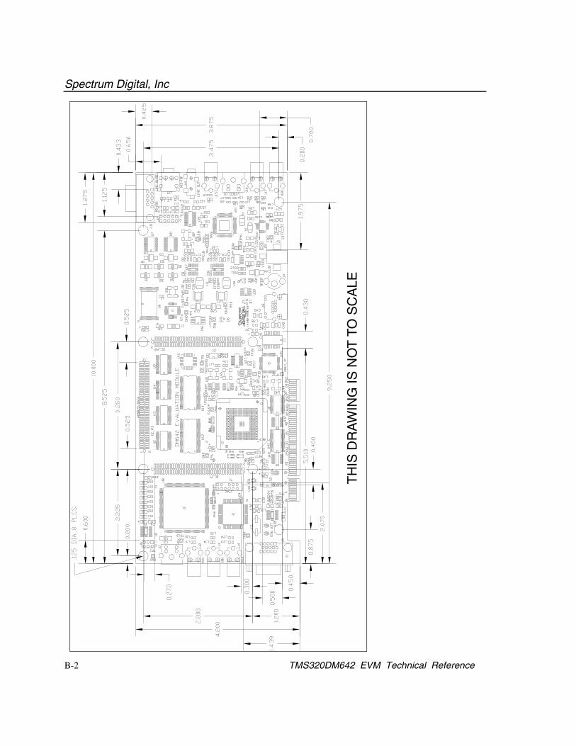
Spectrum Digital, Inc
B-2 TMS320DM642 EVM Technical Reference
TH
IS D
RA
WIN
G IS
NO
T T
O S
CA
LE


Printed in U.S.A., December 2004507345-0001 Rev. B


![OFDM error floor based EVM estimation Error Floor Based EVM Estimation.pdfAWGN source producing the same BER (and EVM) degradation. [1]: The resulting EVM(BER) curves were verified](https://img.pdfslide.net/doc/110x75/5f2e7bc463c3260b31328bb2/ofdm-error-floor-based-evm-estimation-error-floor-based-evm-awgn-source-producing.jpg)