Embed Size (px)
Citation preview
TPS255x-Q1 Precision Automotive Adjustable Current-Limited Power-DistributionSwitches
1 Features• AEC-Q100 Qualified
– Device HBM ESD Classification Level H2– Device CDM ESD Classification Level C5
• Functional Safety-Capable– Documentation available to aid functional safety
system design• Meets USB current-limiting requirements• Adjustable current limit, 500 mA – 5 A (typ.)• ±6.5% current-limit accuracy at 4.5 A• Fast short-circuit response – 3.5 μs (typ.)• 22-mΩ high-side MOSFET• Operating range: 2.5 V to 6.5 V• 2-μA maximum standby supply current• Built-in soft-start• 15-kV and 8-kV system-level ESD capable• Safety-related certifications:
– UL Recognized for UL 2367– CB Certification for IEC 60950– CB Certification for IEC 62368
2 ApplicationAutomotive USB Charging Ports
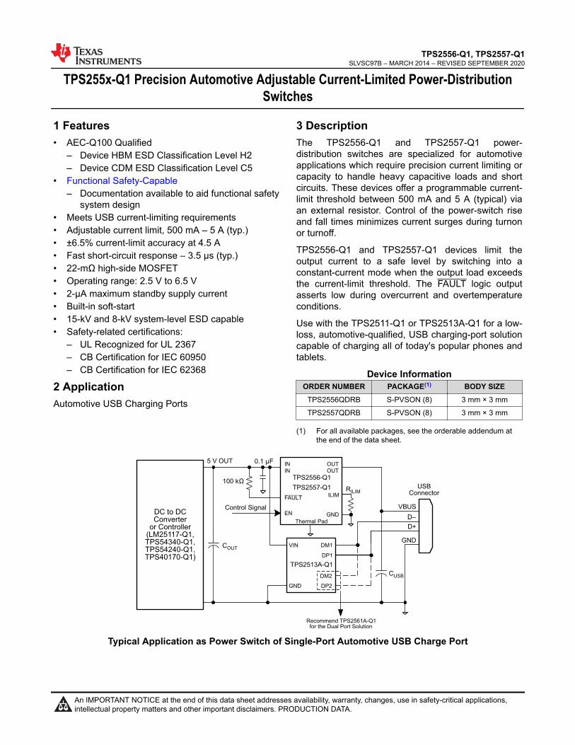
3 DescriptionThe TPS2556-Q1 and TPS2557-Q1 power-distribution switches are specialized for automotiveapplications which require precision current limiting orcapacity to handle heavy capacitive loads and shortcircuits. These devices offer a programmable current-limit threshold between 500 mA and 5 A (typical) viaan external resistor. Control of the power-switch riseand fall times minimizes current surges during turnonor turnoff.
TPS2556-Q1 and TPS2557-Q1 devices limit theoutput current to a safe level by switching into aconstant-current mode when the output load exceedsthe current-limit threshold. The FAULT logic outputasserts low during overcurrent and overtemperatureconditions.
Use with the TPS2511-Q1 or TPS2513A-Q1 for a low-loss, automotive-qualified, USB charging-port solutioncapable of charging all of today's popular phones andtablets.
Device InformationORDER NUMBER PACKAGE(1) BODY SIZE
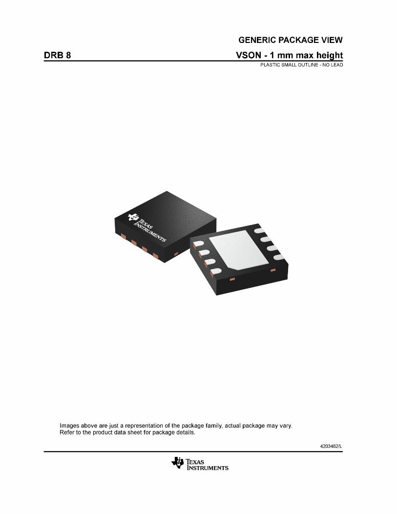
TPS2556QDRB S-PVSON (8) 3 mm × 3 mm
TPS2557QDRB S-PVSON (8) 3 mm × 3 mm
(1) For all available packages, see the orderable addendum atthe end of the data sheet.
DM1
USBConnector
VBUS
D–
D+
GND
5 V OUT
COUT
DC to DCConverter
or Controller(LM25117-Q1,TPS54340-Q1,TPS54240-Q1,TPS40170-Q1)
TPS2513A-Q1
TPS2556-Q1
DP1
DM2
DP2
VIN
GND
RILIM
0.1 μF
IN
IN
EN
FAULT
OUTOUT
ILIM
GND
Thermal Pad
Control Signal
100 kΩTPS2557-Q1
Recommend TPS2561A-Q1for the Dual Port Solution
CUSB
Typical Application as Power Switch of Single-Port Automotive USB Charge Port
www.ti.comTPS2556-Q1, TPS2557-Q1
SLVSC97B – MARCH 2014 – REVISED SEPTEMBER 2020
Copyright © 2020 Texas Instruments Incorporated Submit Document Feedback 1
TPS2556-Q1, TPS2557-Q1SLVSC97B – MARCH 2014 – REVISED SEPTEMBER 2020
An IMPORTANT NOTICE at the end of this data sheet addresses availability, warranty, changes, use in safety-critical applications,intellectual property matters and other important disclaimers. PRODUCTION DATA.
Table of Contents1 Features............................................................................12 Application....................................................................... 13 Description.......................................................................14 Revision History.............................................................. 25 Device Comparison Table...............................................36 Terminal Configuration and Functions..........................37 Specifications.................................................................. 3
7.1 Absolute Maximum Ratings........................................ 37.2 Handling Ratings.........................................................47.3 Recommended Operating Conditions.........................47.4 Thermal Information....................................................47.5 Electrical Characteristics.............................................57.6 Switching Characteristics............................................57.7 Typical Characteristics................................................ 6
8 Parameter Measurement Information............................ 79 Detailed Description........................................................8
9.1 Overview..................................................................... 8
9.2 Functional Block Diagram........................................... 99.3 Feature Description.....................................................99.4 Device Functional Modes..........................................10
10 Applications and Implementation.............................. 1210.1 Application Information........................................... 1210.2 Typical Application, Design for Current Limit.......... 12
11 Power Supply Recommendations..............................1712 Layout...........................................................................18
12.1 Layout Guidelines................................................... 1812.2 Layout Example...................................................... 18
13 Device and Documentation Support..........................1913.1 Related Links.......................................................... 1913.2 Trademarks.............................................................1913.3 Electrostatic Discharge Caution..............................1913.4 Glossary..................................................................19
14 Mechanical, Packaging, and OrderableInformation.................................................................... 20
4 Revision HistoryChanges from Revision A (March 2014) to Revision B (September 2020) Page• Added functional safety link and safety-related certifications bullet to the Features section ............................. 1• Updated the numbering format for tables, figures and cross-references throughout the document...................1
Changes from Revision * (March 2014) to Revision A (March 2014) Page• Changed part number in Description from TPS2511-Q to TPS2511-Q1............................................................ 1• Changed CURRENT LIMIT values in Electrical Characteristics table ............................................................... 5• Changed Equation 1 ........................................................................................................................................ 12• Revised Figure 10-2 graph............................................................................................................................... 12• Changed Equation 2 ........................................................................................................................................ 13• Changed resistor value from 33.2 kΩ to 33.6 kΩ .............................................................................................13• Changed Equation 3 ........................................................................................................................................ 13• Changed Equation 4 ........................................................................................................................................ 14• Changed current-limit threshold from 4 316 mA to 4 406 mA ..........................................................................14• Changed values in Table 10-2 ......................................................................................................................... 14
TPS2556-Q1, TPS2557-Q1SLVSC97B – MARCH 2014 – REVISED SEPTEMBER 2020 www.ti.com
2 Submit Document Feedback Copyright © 2020 Texas Instruments Incorporated
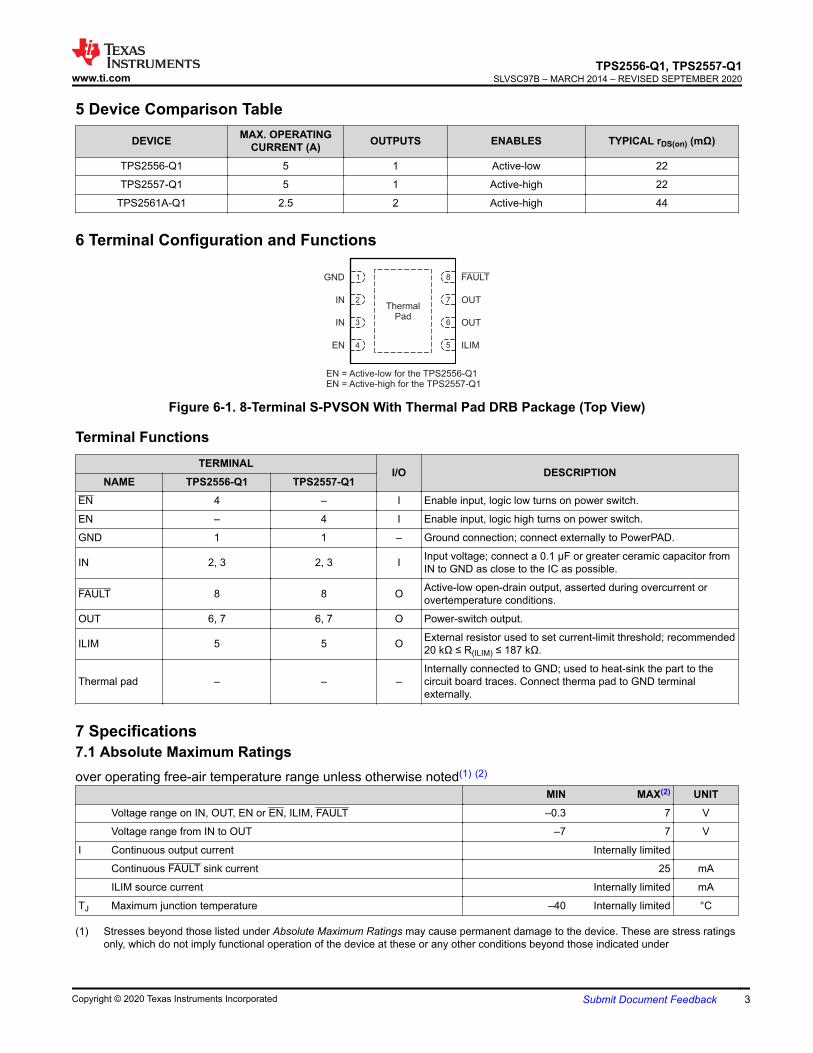
5 Device Comparison Table
DEVICE MAX. OPERATINGCURRENT (A) OUTPUTS ENABLES TYPICAL rDS(on) (mΩ)
TPS2556-Q1 5 1 Active-low 22
TPS2557-Q1 5 1 Active-high 22
TPS2561A-Q1 2.5 2 Active-high 44
6 Terminal Configuration and Functions
GND
IN
IN
EN
FAULT
OUT
OUT
ILIM
1
2
3
4 5
6
7
8
EN = Active-low for the TPS2556-Q1EN = Active-high for the TPS2557-Q1
ThermalPad
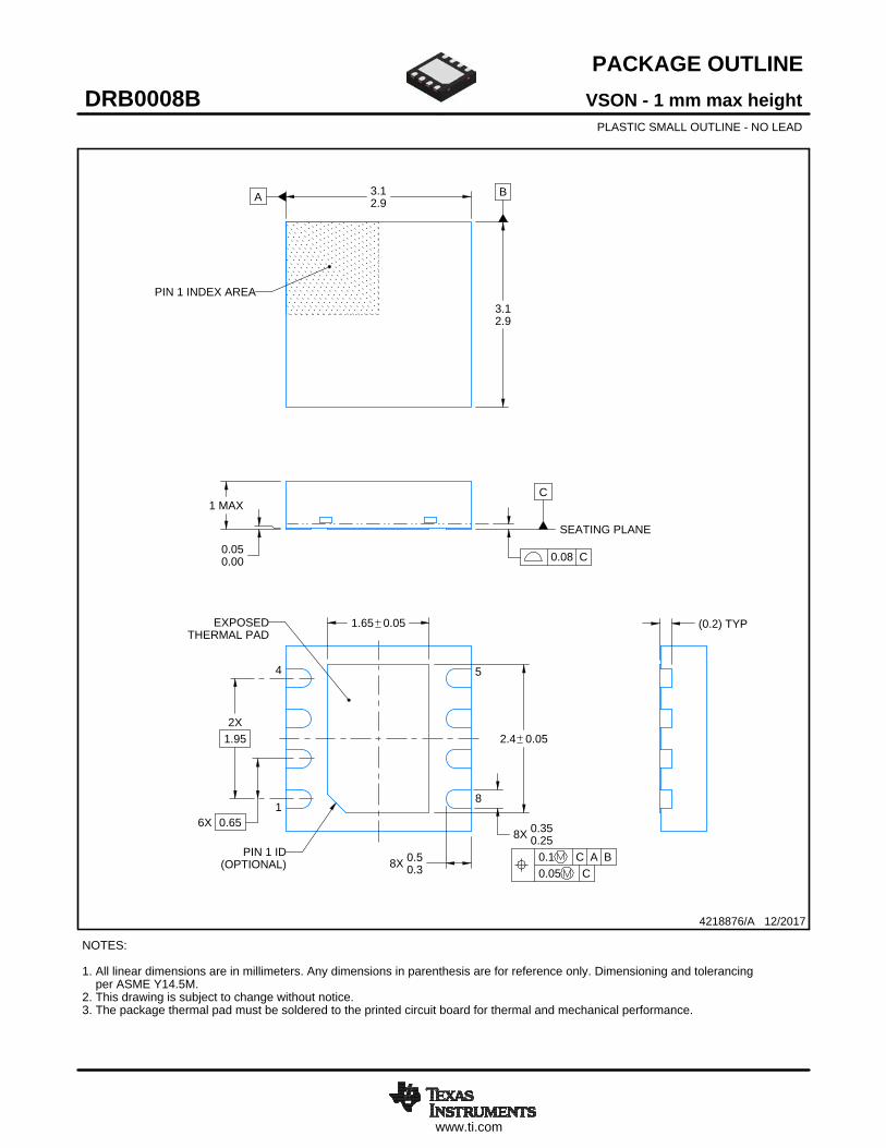
Figure 6-1. 8-Terminal S-PVSON With Thermal Pad DRB Package (Top View)
Terminal FunctionsTERMINAL
I/O DESCRIPTIONNAME TPS2556-Q1 TPS2557-Q1
EN 4 – I Enable input, logic low turns on power switch.
EN – 4 I Enable input, logic high turns on power switch.
GND 1 1 – Ground connection; connect externally to PowerPAD.
IN 2, 3 2, 3 I Input voltage; connect a 0.1 μF or greater ceramic capacitor fromIN to GND as close to the IC as possible.
FAULT 8 8 O Active-low open-drain output, asserted during overcurrent orovertemperature conditions.
OUT 6, 7 6, 7 O Power-switch output.
ILIM 5 5 O External resistor used to set current-limit threshold; recommended20 kΩ ≤ R(ILIM) ≤ 187 kΩ.
Thermal pad – – –Internally connected to GND; used to heat-sink the part to thecircuit board traces. Connect therma pad to GND terminalexternally.
7 Specifications7.1 Absolute Maximum Ratingsover operating free-air temperature range unless otherwise noted(1) (2)
MIN MAX(2) UNITVoltage range on IN, OUT, EN or EN, ILIM, FAULT –0.3 7 V
Voltage range from IN to OUT –7 7 V
I Continuous output current Internally limited
Continuous FAULT sink current 25 mA
ILIM source current Internally limited mA
TJ Maximum junction temperature –40 Internally limited °C
(1) Stresses beyond those listed under Absolute Maximum Ratings may cause permanent damage to the device. These are stress ratingsonly, which do not imply functional operation of the device at these or any other conditions beyond those indicated under
www.ti.comTPS2556-Q1, TPS2557-Q1
SLVSC97B – MARCH 2014 – REVISED SEPTEMBER 2020
Copyright © 2020 Texas Instruments Incorporated Submit Document Feedback 3
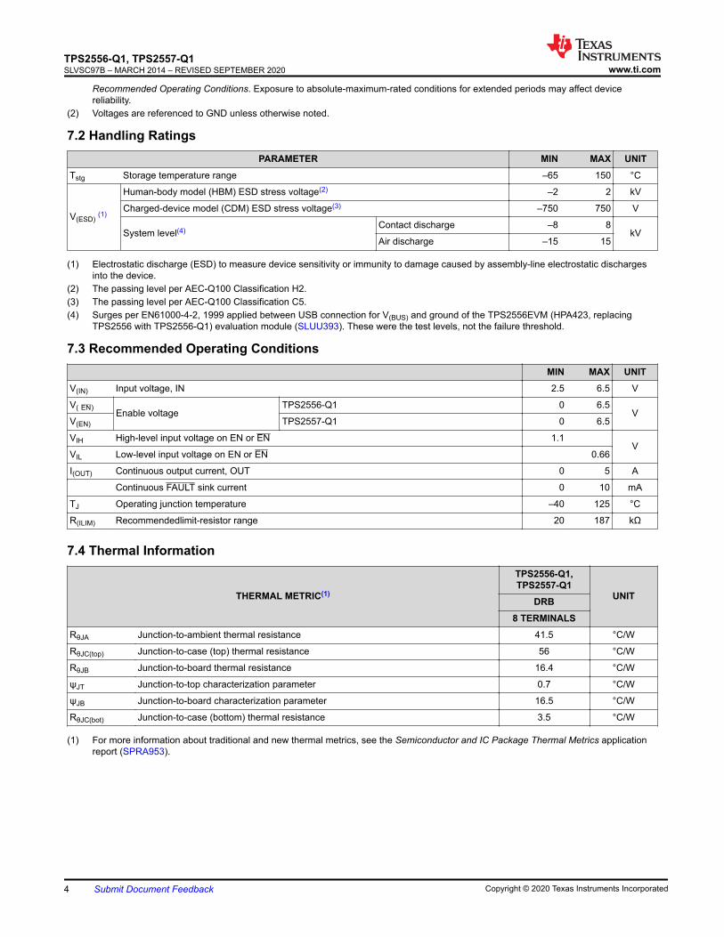
Recommended Operating Conditions. Exposure to absolute-maximum-rated conditions for extended periods may affect devicereliability.
(2) Voltages are referenced to GND unless otherwise noted.
7.2 Handling RatingsPARAMETER MIN MAX UNIT
Tstg Storage temperature range –65 150 °C
V(ESD) (1)
Human-body model (HBM) ESD stress voltage(2) –2 2 kV
Charged-device model (CDM) ESD stress voltage(3) –750 750 V
System level(4)Contact discharge –8 8
kVAir discharge –15 15
(1) Electrostatic discharge (ESD) to measure device sensitivity or immunity to damage caused by assembly-line electrostatic dischargesinto the device.
(2) The passing level per AEC-Q100 Classification H2.(3) The passing level per AEC-Q100 Classification C5.(4) Surges per EN61000-4-2, 1999 applied between USB connection for V(BUS) and ground of the TPS2556EVM (HPA423, replacing
TPS2556 with TPS2556-Q1) evaluation module (SLUU393). These were the test levels, not the failure threshold.
7.3 Recommended Operating ConditionsMIN MAX UNIT
V(IN) Input voltage, IN 2.5 6.5 V
V( EN ) Enable voltageTPS2556-Q1 0 6.5
VV(EN) TPS2557-Q1 0 6.5
VIH High-level input voltage on EN or EN 1.1V
VIL Low-level input voltage on EN or EN 0.66
I(OUT) Continuous output current, OUT 0 5 A
Continuous FAULT sink current 0 10 mA
TJ Operating junction temperature –40 125 °C
R(ILIM) Recommendedlimit-resistor range 20 187 kΩ
7.4 Thermal Information
THERMAL METRIC(1)
TPS2556-Q1,TPS2557-Q1
UNITDRB8 TERMINALS
RθJA Junction-to-ambient thermal resistance 41.5 °C/W
RθJC(top) Junction-to-case (top) thermal resistance 56 °C/W
RθJB Junction-to-board thermal resistance 16.4 °C/W
ψJT Junction-to-top characterization parameter 0.7 °C/W
ψJB Junction-to-board characterization parameter 16.5 °C/W
RθJC(bot) Junction-to-case (bottom) thermal resistance 3.5 °C/W
(1) For more information about traditional and new thermal metrics, see the Semiconductor and IC Package Thermal Metrics applicationreport (SPRA953).
TPS2556-Q1, TPS2557-Q1SLVSC97B – MARCH 2014 – REVISED SEPTEMBER 2020 www.ti.com
4 Submit Document Feedback Copyright © 2020 Texas Instruments Incorporated
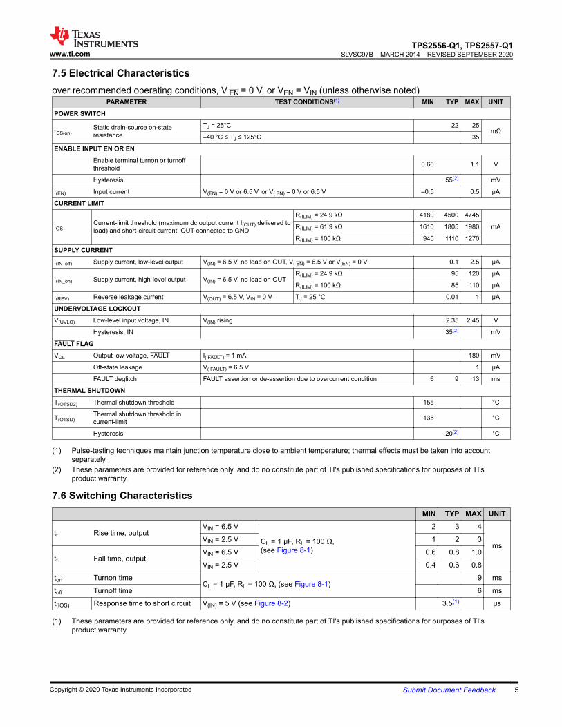
7.5 Electrical Characteristicsover recommended operating conditions, V EN = 0 V, or VEN = VIN (unless otherwise noted)
PARAMETER TEST CONDITIONS(1) MIN TYP MAX UNIT
POWER SWITCH
rDS(on)Static drain-source on-stateresistance
TJ = 25°C 22 25mΩ
–40 °C ≤ TJ ≤ 125°C 35
ENABLE INPUT EN OR EN
Enable terminal turnon or turnoffthreshold 0.66 1.1 V
Hysteresis 55(2) mV
I(EN) Input current V(EN) = 0 V or 6.5 V, or V( EN) = 0 V or 6.5 V –0.5 0.5 μA
CURRENT LIMIT
IOSCurrent-limit threshold (maximum dc output current I(OUT) delivered toload) and short-circuit current, OUT connected to GND
R(ILIM) = 24.9 kΩ 4180 4500 4745
mAR(ILIM) = 61.9 kΩ 1610 1805 1980
R(ILIM) = 100 kΩ 945 1110 1270
SUPPLY CURRENT
I(IN_off) Supply current, low-level output V(IN) = 6.5 V, no load on OUT, V( EN) = 6.5 V or V(EN) = 0 V 0.1 2.5 μA
I(IN_on) Supply current, high-level output V(IN) = 6.5 V, no load on OUTR(ILIM) = 24.9 kΩ 95 120 μA
R(ILIM) = 100 kΩ 85 110 μA
I(REV) Reverse leakage current V(OUT) = 6.5 V, VIN = 0 V TJ = 25 °C 0.01 1 μA
UNDERVOLTAGE LOCKOUT
V(UVLO) Low-level input voltage, IN V(IN) rising 2.35 2.45 V
Hysteresis, IN 35(2) mV
FAULT FLAG
VOL Output low voltage, FAULT I( FAULT) = 1 mA 180 mV
Off-state leakage V( FAULT) = 6.5 V 1 μA
FAULT deglitch FAULT assertion or de-assertion due to overcurrent condition 6 9 13 ms
THERMAL SHUTDOWN
T(OTSD2) Thermal shutdown threshold 155 °C
T(OTSD)Thermal shutdown threshold incurrent-limit 135 °C
Hysteresis 20(2) °C
(1) Pulse-testing techniques maintain junction temperature close to ambient temperature; thermal effects must be taken into accountseparately.
(2) These parameters are provided for reference only, and do no constitute part of TI's published specifications for purposes of TI'sproduct warranty.
7.6 Switching CharacteristicsMIN TYP MAX UNIT
tr Rise time, outputVIN = 6.5 V
CL = 1 μF, RL = 100 Ω,(see Figure 8-1)
2 3 4
msVIN = 2.5 V 1 2 3
tf Fall time, outputVIN = 6.5 V 0.6 0.8 1.0
VIN = 2.5 V 0.4 0.6 0.8
ton Turnon timeCL = 1 μF, RL = 100 Ω, (see Figure 8-1)
9 ms
toff Turnoff time 6 ms
t(IOS) Response time to short circuit V(IN) = 5 V (see Figure 8-2) 3.5(1) μs
(1) These parameters are provided for reference only, and do no constitute part of TI's published specifications for purposes of TI'sproduct warranty
www.ti.comTPS2556-Q1, TPS2557-Q1
SLVSC97B – MARCH 2014 – REVISED SEPTEMBER 2020
Copyright © 2020 Texas Instruments Incorporated Submit Document Feedback 5
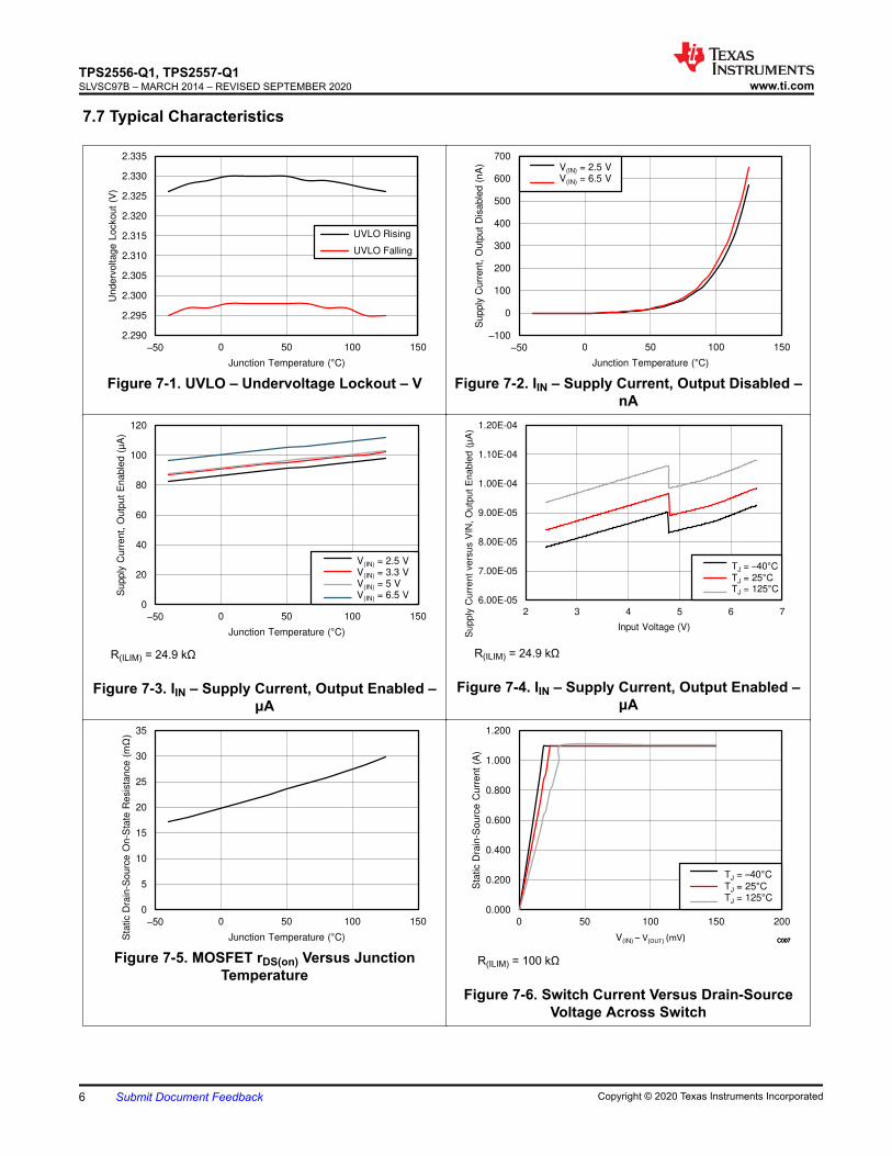
7.7 Typical Characteristics
2.290
2.295
2.300
2.305
2.310
2.315
2.320
2.325
2.330
2.335
±50 0 50 100 150
Underv
oltage L
ockout
(V)
Junction Temperature (C)
UVLO Rising
UVLO Falling
C001
Figure 7-1. UVLO – Undervoltage Lockout – V
±100
0
100
200
300
400
500
600
700
±50 0 50 100 150
Supply
Curr
ent, O
utp
ut
Dis
able
d (
nA
)
Junction Temperature (C)
VIN = 2.5 V
VIN = 6.5 V
C002
V(IN) = 2.5 V V(IN) = 6.5 V
Figure 7-2. IIN – Supply Current, Output Disabled –nA
0
20
40
60
80
100
120
±50 0 50 100 150
Supply
Cu
rrent, O
utp
ut
Enable
d (
µA
)
Junction Temperature (C)
VIN = 2.5 V
VIN = 3.3 V
VIN = 5 V
VIN = 6.5 V
C003
V(IN) = 2.5 V V(IN) = 3.3 V V(IN) = 5 V V(IN) = 6.5 V
R(ILIM) = 24.9 kΩ
Figure 7-3. IIN – Supply Current, Output Enabled –μA
6.00E-05
7.00E-05
8.00E-05
9.00E-05
1.00E-04
1.10E-04
1.20E-04
2 3 4 5 6 7
Supply
Curr
ent
vers
us V
IN,
Outp
ut
Enable
d (
µA
)
Input Voltage (V)
TJ = ±40
TJ = 25
TJ = 125
C004
TJ = t40C
TJ = 25C TJ = 125C
R(ILIM) = 24.9 kΩ
Figure 7-4. IIN – Supply Current, Output Enabled –μA
0
5
10
15
20
25
30
35
±50 0 50 100 150
Sta
tic D
rain
-Sourc
e O
n-S
tate
Re
sis
tance (
m
Junction Temperature (C) C005
Figure 7-5. MOSFET rDS(on) Versus JunctionTemperature
0.000
0.200
0.400
0.600
0.800
1.000
1.200
0 50 100 150 200
Sta
tic D
rain
-Sourc
e C
urr
ent
(A)
V(IN) t V(OUT) (mV)
TA = -40°C
TA = 25°C
TA = 125°C
C006 C007
TA = t40C
TA = 25C TA =125C
C007
TA = t40C
TA = 25C TA =125C
C007
TJ = t40C
TJ = 25C TJ = 125C
R(ILIM) = 100 kΩ
Figure 7-6. Switch Current Versus Drain-SourceVoltage Across Switch
TPS2556-Q1, TPS2557-Q1SLVSC97B – MARCH 2014 – REVISED SEPTEMBER 2020 www.ti.com
6 Submit Document Feedback Copyright © 2020 Texas Instruments Incorporated
0.0
0.2
0.4
0.6
0.8
1.0
1.2
1.4
1.6
1.8
2.0
0 50 100 150 200
Sta
tic D
rain
-Sourc
e C
urr
ent
(A)
V(IN) ± V(OUT) (mV)
TA = ±40C
TA = 25°C
TA = 125°C
C007
TJ = t40C
TJ = 25C TJ = 125C
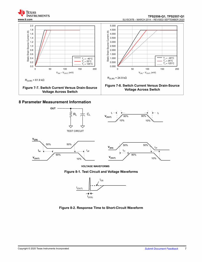
R(ILIM) = 61.9 kΩ
Figure 7-7. Switch Current Versus Drain-SourceVoltage Across Switch
0.000
0.500
1.000
1.500
2.000
2.500
3.000
3.500
4.000
4.500
5.000
0 50 100 150 200
Sta
tic D
rain
-Sourc
e C
urr
ent
(A)
V(IN) ± V(OUT) (mV)
TJ = ±40C
TJ = 25°C
TJ = 125°C
C010
TJ = t40C
TJ = 25C TJ = 125C
R(ILIM) = 24.9 kΩ
Figure 7-8. Switch Current Versus Drain-SourceVoltage Across Switch
8 Parameter Measurement Information
RL CL
OUT
TEST CIRCUIT
tr tf
10%
90%
10%
90%
ton
10%
90%
50%50%
V( )EN
V(OUT)
ton
toff
50% 50%
10%
90%
VOLTAGE WAVEFORMS
toff
tn
V(OUT)
V(OUT)
V(EN)
Figure 8-1. Test Circuit and Voltage Waveforms
t(IOS)
IOS
I(OUT)
Figure 8-2. Response Time to Short-Circuit Waveform
www.ti.comTPS2556-Q1, TPS2557-Q1
SLVSC97B – MARCH 2014 – REVISED SEPTEMBER 2020
Copyright © 2020 Texas Instruments Incorporated Submit Document Feedback 7
V(OUT)
I(OUT)
IOS
DecreasingLoad Resistance
DecreasingLoad Resistance
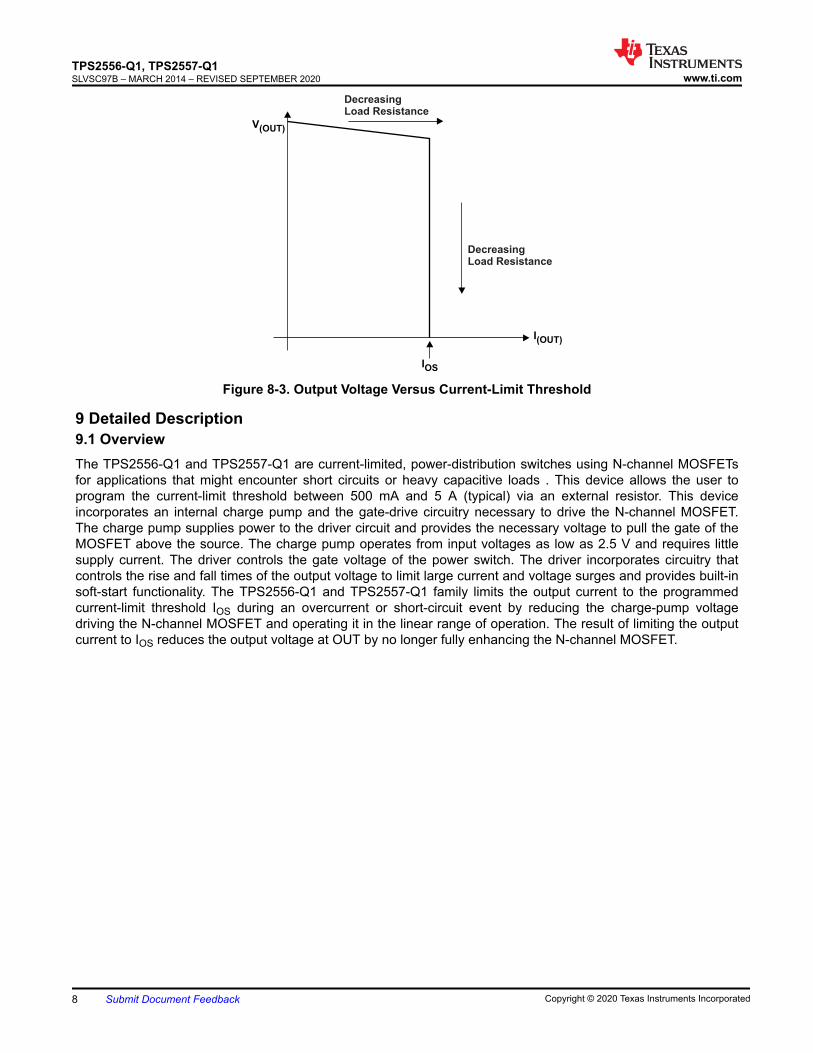
Figure 8-3. Output Voltage Versus Current-Limit Threshold
9 Detailed Description9.1 OverviewThe TPS2556-Q1 and TPS2557-Q1 are current-limited, power-distribution switches using N-channel MOSFETsfor applications that might encounter short circuits or heavy capacitive loads . This device allows the user toprogram the current-limit threshold between 500 mA and 5 A (typical) via an external resistor. This deviceincorporates an internal charge pump and the gate-drive circuitry necessary to drive the N-channel MOSFET.The charge pump supplies power to the driver circuit and provides the necessary voltage to pull the gate of theMOSFET above the source. The charge pump operates from input voltages as low as 2.5 V and requires littlesupply current. The driver controls the gate voltage of the power switch. The driver incorporates circuitry thatcontrols the rise and fall times of the output voltage to limit large current and voltage surges and provides built-insoft-start functionality. The TPS2556-Q1 and TPS2557-Q1 family limits the output current to the programmedcurrent-limit threshold IOS during an overcurrent or short-circuit event by reducing the charge-pump voltagedriving the N-channel MOSFET and operating it in the linear range of operation. The result of limiting the outputcurrent to IOS reduces the output voltage at OUT by no longer fully enhancing the N-channel MOSFET.
TPS2556-Q1, TPS2557-Q1SLVSC97B – MARCH 2014 – REVISED SEPTEMBER 2020 www.ti.com
8 Submit Document Feedback Copyright © 2020 Texas Instruments Incorporated
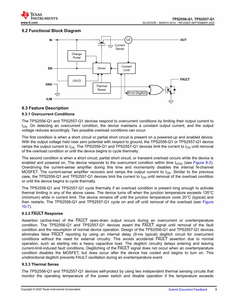
9.2 Functional Block Diagram
Charge
Pump
Driver
UVLO
Current
Limit
Thermal
Sense8-ms Deglitch
IN
GND
EN
ILIM
OUT
FAULT
CS
Current
Sense
9.3 Feature Description9.3.1 Overcurrent Conditions
The TPS2556-Q1 and TPS2557-Q1 devices respond to overcurrent conditions by limiting their output current toIOS. On detecting an overcurrent condition, the device maintains a constant output current, and the outputvoltage reduces accordingly. Two possible overload conditions can occur.
The first condition is when a short circuit or partial short circuit is present on a powered-up and enabled device.With the output voltage held near zero potential with respect to ground, the TPS2556-Q1 or TPS2557-Q1 deviceramps the output current to IOS. The TPS2556-Q1 and TPS2557-Q1 devices limit the current to IOS until removalof the overload condition or until the device begins to cycle thermally.
The second condition is when a short circuit, partial short circuit, or transient overload occurs while the device isenabled and powered on. The device responds to the overcurrent condition within time t(IOS) (see Figure 8-2).Overdriving the current-sense amplifier during this time and momentarily disables the internal N-channelMOSFET. The current-sense amplifier recovers and ramps the output current to IOS. Similar to the previouscase, the TPS2556-Q1 and TPS2557-Q1 devices limit the current to IOS until removal of the overload conditionor until the device begins to cycle thermally.
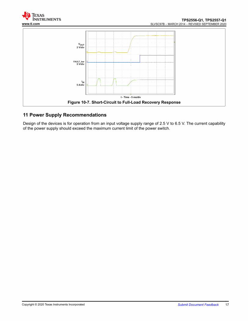
The TPS2556-Q1 and TPS2557-Q1 cycle thermally if an overload condition is present long enough to activatethermal limiting in any of the above cases. The device turns off when the junction temperature exceeds 135°C(minimum) while in current limit. The device remains off until the junction temperature cools 20°C (typical) andthen restarts. The TPS2556-Q1 and TPS2557-Q1 cycle on and off until removal of the overload (see Figure10-7).
9.3.2 FAULT Response
Assertion (active-low) of the FAULT open-drain output occurs during an overcurrent or overtemperaturecondition. The TPS2556-Q1 and TPS2557-Q1 devices assert the FAULT signal until removal of the faultcondition and the resumption of normal device operation. Design of the TPS2556-Q1 and TPS2557-Q1 deviceseliminates false FAULT reporting by using an internal delay (9-ms typical) deglitch circuit for overcurrentconditions without the need for external circuitry. This avoids accidental FAULT assertion due to normaloperation, such as starting into a heavy capacitive load. The deglitch circuitry delays entering and leavingcurrent-limit-induced fault conditions. Deglitching of the FAULT signal does not occur when an overtemperaturecondition disables the MOSFET, but does occur after the device has cooled and begins to turn on. Thisunidirectional deglitch prevents FAULT oscillation during an overtemperature event.
9.3.3 Thermal Sense
The TPS2556-Q1 and TPS2557-Q1 devices self-protect by using two independent thermal sensing circuits thatmonitor the operating temperature of the power switch and disable operation if the temperature exceeds
www.ti.comTPS2556-Q1, TPS2557-Q1
SLVSC97B – MARCH 2014 – REVISED SEPTEMBER 2020
Copyright © 2020 Texas Instruments Incorporated Submit Document Feedback 9
recommended operating conditions. The TPS2556-Q1 and TPS2557-Q1 devices operate in constant-currentmode during an overcurrent condition, which increases the voltage drop across power switch. The powerdissipation in the package is proportional to the voltage drop across the power switch, which increases thejunction temperature during an overcurrent condition. The first thermal sensor (OTSD) turns off the power switchwhen the die temperature exceeds 135°C (min) and the part is in current limit. Hysteresis is built into the thermalsensor, and the switch turns on after the device has cooled approximately 20°C.
The TPS2556-Q1 and TPS2557-Q1 devices also have a second thermal sensor (OTSD2). This thermal sensorturns off the power switch when the die temperature exceeds 155°C (minimum) regardless of whether the powerswitch is in current limit, and turns on the power switch after the device has cooled approximately 20°C. TheTPS2556-Q1 and TPS2557-Q1 devices continue to cycle off and on until the fault is removed.
9.4 Device Functional Modes9.4.1 Undervoltage Lockout (UVLO)
The undervoltage lockout (UVLO) circuit disables the power switch until the input voltage reaches the UVLOturnon threshold. Built-in hysteresis prevents unwanted on-and-off cycling due to input voltage droop duringturnon.
9.4.2 Enable ( EN OR EN)
The logic enable controls the power switch and device supply current. The supply current is reduced to less than2 μA when a logic high is present on EN or when a logic low is present on EN. A logic low input on EN or a logichigh input on EN enables the driver, control circuits, and power switch. The enable input is compatible with bothTTL and CMOS logic levels.
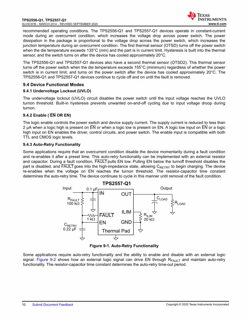
9.4.3 Auto-Retry Functionality
Some applications require that an overcurrent condition disable the device momentarily during a fault conditionand re-enables it after a preset time. This auto-retry functionality can be implemented with an external resistorand capacitor. During a fault condition, FAULT pulls EN low. Pulling EN below the turnoff threshold disables thepart is disabled, and FAULT goes into the high-impedance state, allowing CRETRY to begin charging. The devicere-enables when the voltage on EN reaches the turnon threshold. The resistor-capacitor time constantdetermines the auto-retry time. The device continues to cycle in this manner until removal of the fault condition.
OUTIN
GND
FAULTILIM
EN20 kW
100 kW
InputTPS2557-Q1
0.1 µF
Thermal Pad
RLOAD
0.22 µF
Output
1 kW
CLOAD
RILIM
RFAULT
CRETRY
Figure 9-1. Auto-Retry Functionality
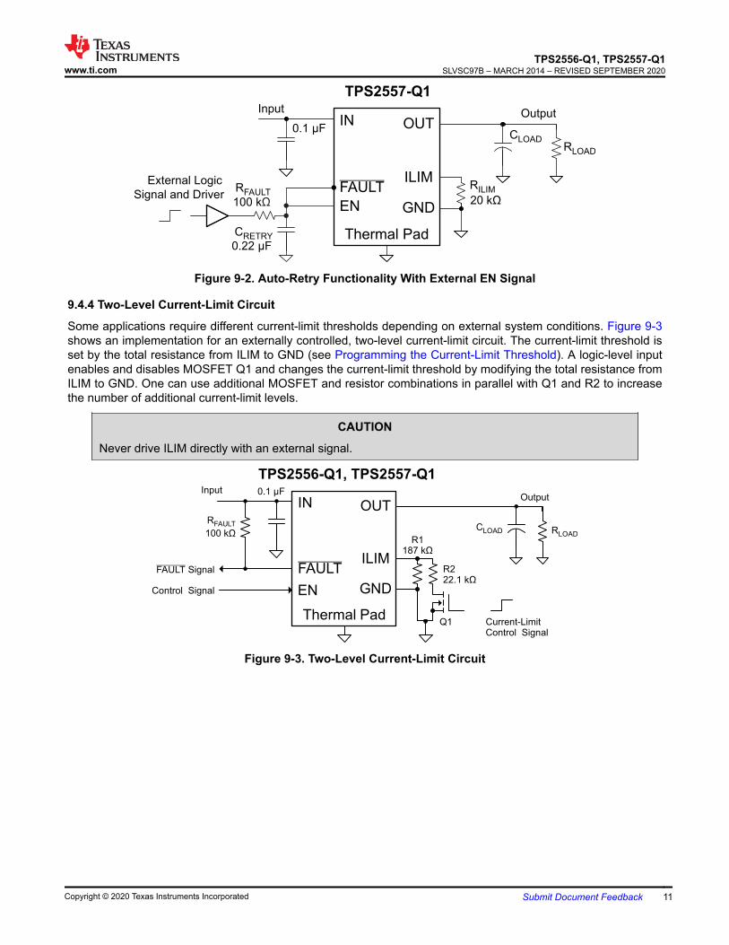
Some applications require auto-retry functionality and the ability to enable and disable with an external logicsignal. Figure 9-2 shows how an external logic signal can drive EN through RFAULT and maintain auto-retryfunctionality. The resistor-capacitor time constant determines the auto-retry time-out period.
TPS2556-Q1, TPS2557-Q1SLVSC97B – MARCH 2014 – REVISED SEPTEMBER 2020 www.ti.com
10 Submit Document Feedback Copyright © 2020 Texas Instruments Incorporated
OUTIN
GND
FAULTILIM
EN 20 kΩ100 kΩ
External Logic
Signal and Driver
TPS2557-Q1
0.1 µF
Thermal Pad
RLOAD
0.22 µF
OutputInput
CLOAD
RILIMRFAULT
CRETRY
Figure 9-2. Auto-Retry Functionality With External EN Signal
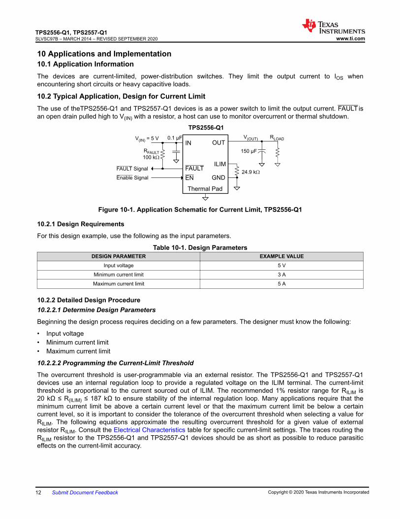
9.4.4 Two-Level Current-Limit Circuit
Some applications require different current-limit thresholds depending on external system conditions. Figure 9-3shows an implementation for an externally controlled, two-level current-limit circuit. The current-limit threshold isset by the total resistance from ILIM to GND (see Programming the Current-Limit Threshold). A logic-level inputenables and disables MOSFET Q1 and changes the current-limit threshold by modifying the total resistance fromILIM to GND. One can use additional MOSFET and resistor combinations in parallel with Q1 and R2 to increasethe number of additional current-limit levels.
CAUTION
Never drive ILIM directly with an external signal.
OUTIN
GND
FAULTILIM
EN
R1187 kΩ
RFAULT
100 kΩ
Control Signal
Input
TPS2556-Q1, TPS2557-Q10.1 µF
FAULT Signal
Thermal Pad
Output
R222.1 kΩ
Current-LimitControl Signal
RLOAD
Q1
CLOAD
Figure 9-3. Two-Level Current-Limit Circuit
www.ti.comTPS2556-Q1, TPS2557-Q1
SLVSC97B – MARCH 2014 – REVISED SEPTEMBER 2020
Copyright © 2020 Texas Instruments Incorporated Submit Document Feedback 11
10 Applications and Implementation10.1 Application InformationThe devices are current-limited, power-distribution switches. They limit the output current to IOS whenencountering short circuits or heavy capacitive loads.
10.2 Typical Application, Design for Current LimitThe use of theTPS2556-Q1 and TPS2557-Q1 devices is as a power switch to limit the output current. FAULT isan open drain pulled high to V(IN) with a resistor, a host can use to monitor overcurrent or thermal shutdown.
OUTIN
GND
FAULTILIM
EN24.9 kW
RFAULT
100 kW
Enable Signal
V = 5 V(IN)
TPS2556-Q1
150 µF
FAULT Signal
Thermal Pad
RLOADV(OUT)0.1 µF
Figure 10-1. Application Schematic for Current Limit, TPS2556-Q1
10.2.1 Design Requirements
For this design example, use the following as the input parameters.
Table 10-1. Design ParametersDESIGN PARAMETER EXAMPLE VALUE
Input voltage 5 V
Minimum current limit 3 A
Maximum current limit 5 A
10.2.2 Detailed Design Procedure10.2.2.1 Determine Design Parameters
Beginning the design process requires deciding on a few parameters. The designer must know the following:
• Input voltage• Minimum current limit• Maximum current limit
10.2.2.2 Programming the Current-Limit Threshold
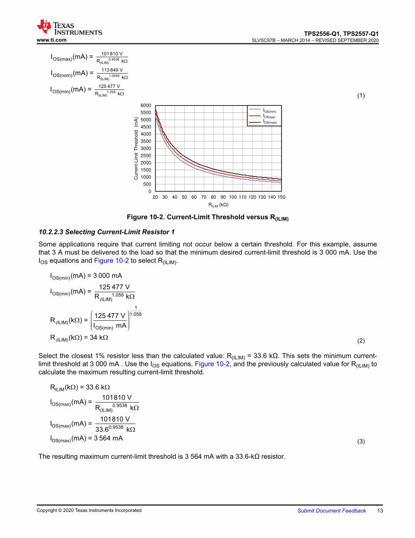
The overcurrent threshold is user-programmable via an external resistor. The TPS2556-Q1 and TPS2557-Q1devices use an internal regulation loop to provide a regulated voltage on the ILIM terminal. The current-limitthreshold is proportional to the current sourced out of ILIM. The recommended 1% resistor range for RILIM is20 kΩ ≤ R(ILIM) ≤ 187 kΩ to ensure stability of the internal regulation loop. Many applications require that theminimum current limit be above a certain current level or that the maximum current limit be below a certaincurrent level, so it is important to consider the tolerance of the overcurrent threshold when selecting a value forRILIM. The following equations approximate the resulting overcurrent threshold for a given value of externalresistor RILIM. Consult the Electrical Characteristics table for specific current-limit settings. The traces routing theRILIM resistor to the TPS2556-Q1 and TPS2557-Q1 devices should be as short as possible to reduce parasiticeffects on the current-limit accuracy.
TPS2556-Q1, TPS2557-Q1SLVSC97B – MARCH 2014 – REVISED SEPTEMBER 2020 www.ti.com
12 Submit Document Feedback Copyright © 2020 Texas Instruments Incorporated
0.9538(ILIM)
1.0049(ILIM)
1.058(ILIM)
101 810 VOS(max) R k
113 849 VOS(nom) R k
125 477 VOS(min) R k
I (mA) =
I (mA) =
I (mA) =
W
W
W (1)
0
500
1000
1500
2000
2500
3000
3500
4000
4500
5000
5500
6000
20 30 40 50 60 70 80 90 100 110 120 130 140 150
Curr
ent-
Lim
it T
hre
shold
(m
A)
RILIM N
Power (min)
Power (typ)
Power (max)
C002
IOS(min) IOS(typ)
IOS(max)
Figure 10-2. Current-Limit Threshold versus R(ILIM)
10.2.2.3 Selecting Current-Limit Resistor 1
Some applications require that current limiting not occur below a certain threshold. For this example, assumethat 3 A must be delivered to the load so that the minimum desired current-limit threshold is 3 000 mA. Use theIOS equations and Figure 10-2 to select R(ILIM).
(
(
(
OS(min)
OS(min) 1.058ILIM)
1
1.058
ILIM)OS(min)
ILIM)
I (mA) = 3 000 mA
125 477 VI (mA) =
R k
125 477 VR (k ) =
I mA
R (k ) = 34 k
W
W
W W
æ ö÷ç ÷ç ÷ç ÷ç ÷çè ø
(2)
Select the closest 1% resistor less than the calculated value: R(ILIM) = 33.6 kΩ. This sets the minimum current-limit threshold at 3 000 mA . Use the IOS equations, Figure 10-2, and the previously calculated value for R(ILIM) tocalculate the maximum resulting current-limit threshold.
ILIM
OS(max) 0.9538(ILIM)
OS(max) 0.9538
OS(max)
R (k ) = 33.6 k
101810 VI (mA) =
R k
101810 VI (mA) =
33.6 k
I (mA) = 3 564 mA
W W
W
W
(3)
The resulting maximum current-limit threshold is 3 564 mA with a 33.6-kΩ resistor.
www.ti.comTPS2556-Q1, TPS2557-Q1
SLVSC97B – MARCH 2014 – REVISED SEPTEMBER 2020
Copyright © 2020 Texas Instruments Incorporated Submit Document Feedback 13
10.2.2.4 Selecting Current-Limit Resistor 2
Some applications require that current limiting must occur below a certain threshold. For this example, assumethat the desired upper current-limit threshold must be below 5,000 mA to protect an upstream power supply. Usethe IOS equations and Figure 10-2 to select R(ILIM).
(
(
(
OS(max)
OS(max) 0.9538ILIM)
1
0.9538
ILIM)OS(max)
ILIM)
I (mA) = 5 000 mA
101 810 VI (mA) =
R k
101 810 VR (k ) =
I mA
R (k ) = 23.6 k
W
W
W W
æ ö÷ç ÷ç ÷ç ÷ç ÷çè ø
(4)
Select the closest 1% resistor greater than the calculated value: R(ILIM) = 23.7 kΩ. This sets the maximumcurrent-limit threshold at 5 000 mA . Use the IOS equations, Figure 10-2, and the previously calculated value forRILIM to calculate the minimum resulting current-limit threshold.
(ILIM)
OS(min) 1.058(ILIM)
OS(min) 1.058
OS(min)
R (k ) = 23.7 k
125 477 VI (mA) =
R
125 477 VI (mA) =
23.7
I (mA) = 4 406 mA
W W
(5)
The resulting minimum current-limit threshold is 4 406 mA with a 23.7-kΩ resistor.
10.2.2.5 Accounting for Resistor Tolerance
The previous sections described the selection of RILIM given certain application requirements and the importanceof understanding the current-limit threshold tolerance. The analysis focused only on the TPS2556-Q1 andTPS2557-Q1 device performance and assumed an exact resistor value. However, resistors sold in quantity arenot exact and are bounded by an upper and lower tolerance centered around a nominal resistance. Theadditional RILIM resistance tolerance directly affects the current-limit threshold accuracy at a system level. Thefollowing table shows a process that accounts for worst-case resistor tolerance assuming 1% resistor values.Step one follows the selection process outlined in the foregoing application examples. Step two determines theupper and lower resistance bounds of the selected resistor. Step three uses the upper and lower resistor boundsin the IOS equations to calculate the threshold limits. It is important to use tighter tolerance resistors, for example0.5% or 0.1%, when precision current limiting is desirable.
TPS2556-Q1, TPS2557-Q1SLVSC97B – MARCH 2014 – REVISED SEPTEMBER 2020 www.ti.com
14 Submit Document Feedback Copyright © 2020 Texas Instruments Incorporated
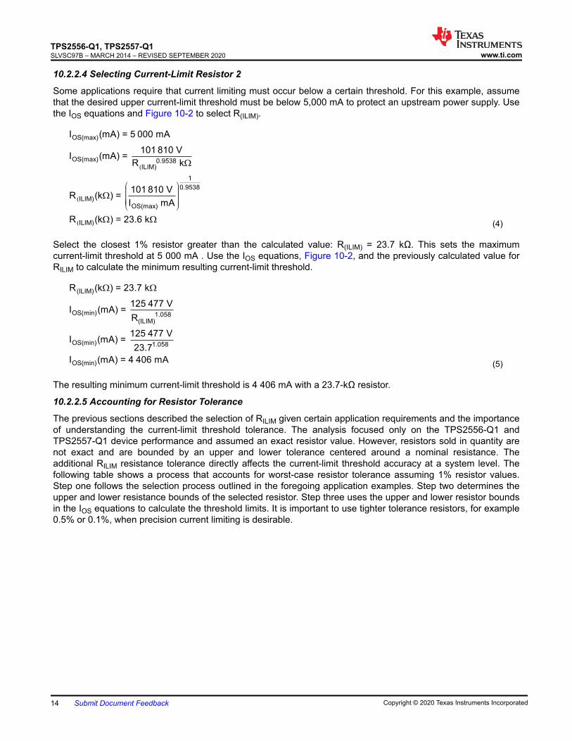
Table 10-2. Common RILIM Resistor SelectionsDesired Nominal
Current Limit (mA)Ideal Resistor
(kΩ)Closest 1%
Resistor (kΩ)Resistor Tolerance Actual Limits
1% low (kΩ) 1% high (kΩ) IOS MIN (mA) IOS NOM (mA) IOS MAX (mA)750 148.1 147 145.5 148.5 632 756 881
1000 111.3 110 108.9 111.1 859 1011 1161
1250 89.1 88.7 87.8 89.6 1079 1256 1426
1500 74.3 75 74.3 75.8 1289 1486 1673
1750 63.7 63.4 62.8 64.0 1540 1760 1964
2000 55.8 56.2 55.6 56.8 1749 1986 2203
2250 49.6 49.9 49.4 50.4 1983 2238 2468
2500 44.7 44.2 43.8 44.6 2255 2528 2770
2750 40.7 40.2 39.8 40.6 2493 2781 3033
3000 37.3 37.4 37.0 37.8 2691 2991 3249
3250 34.4 34.8 34.5 35.1 2904 3215 3480
3500 32.0 31.6 31.3 31.9 3216 3542 3816
3750 29.9 30.1 29.8 30.4 3386 3720 3997
4000 28.0 28 27.7 28.3 3655 4000 4282
4250 26.4 26.1 25.8 26.4 3937 4293 4579
4500 24.9 24.9 24.7 25.1 4138 4501 4789
4750 23.6 23.7 23.5 23.9 4360 4730 5020
5000 22.4 22.6 22.4 22.8 4585 4961 5253
5250 21.4 21.5 21.3 21.7 4834 5216 5509
5500 20.4 20.5 20.3 20.7 5083 5472 5765
10.2.2.6 Power Dissipation and Junction Temperature
The low on-resistance of the N-channel MOSFET allows small surface-mount packages to pass large currents. Itis good design practice to estimate power dissipation and junction temperature. The following analysis gives anapproximation for calculating junction temperature based on the power dissipation in the package. However, it isimportant to note that thermal analysis is strongly dependent on additional system-level factors. Such factorsinclude air flow, board layout, copper thickness and surface area, and proximity to other devices that dissipatepower. Good thermal design practice must include all system-level factors in addition to individual componentanalysis.
Begin by determining the rDS(on) of the N-channel MOSFET relative to the input voltage and operatingtemperature. As an initial estimate, use the highest operating ambient temperature of interest and read rDS(on)from the typical characteristics graph. Using this value, calculate the power dissipation by:
PD = rDS(on) × IOUT 2
where:
PD = Total power dissipation (W)
rDS(on) = Power-switch on-resistance (Ω)
I(OUT) = Maximum current-limit threshold (A)
This step calculates the total power dissipation of the N-channel MOSFET.
Finally, calculate the junction temperature:
TJ = PD × RθJA + TA
where:
TA = Ambient temperature (°C)
www.ti.comTPS2556-Q1, TPS2557-Q1
SLVSC97B – MARCH 2014 – REVISED SEPTEMBER 2020
Copyright © 2020 Texas Instruments Incorporated Submit Document Feedback 15
RθJA = Thermal resistance (°C/W)
PD = Total power dissipation (W)
Compare the calculated junction temperature with the initial estimate. If they are not within a few degrees, repeatthe calculation using the refined rDS(on) from the previous calculation as the new estimate. Two or three iterationsare generally sufficient to achieve the desired result. The final junction temperature is highly dependent onthermal resistance RθJA, and thermal resistance is highly dependent on the individual package and board layout.The Thermal Information table lists thermal resistances of the device that one can use to help calculate thethermal performance of the board design.
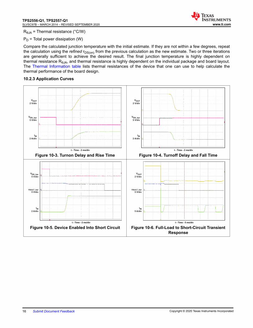
10.2.3 Application Curves
V
2 V/divOUT
V
5 V/divEN_bar
t - Time - 2 ms/div
I
2 A/divIN
Figure 10-3. Turnon Delay and Rise Time
V
2 V/divOUT
V
5 V/divEN_bar
t - Time - 2 ms/div
I
2 A/divIN
Figure 10-4. Turnoff Delay and Fall Time
V
5 V/divEN_bar
FAULT_bar
5 V/div
t - Time - 2 ms/div
I
2 A/divIN
Figure 10-5. Device Enabled Into Short Circuit
V
2 V/divOUT
FAULT_bar
5 V/div
t - Time - 5 ms/div
I
5 A/divIN
Figure 10-6. Full-Load to Short-Circuit TransientResponse
TPS2556-Q1, TPS2557-Q1SLVSC97B – MARCH 2014 – REVISED SEPTEMBER 2020 www.ti.com
16 Submit Document Feedback Copyright © 2020 Texas Instruments Incorporated
V
2 V/divOUT
FAULT_bar
5 V/div
t - Time - 5 ms/div
I
5 A/divIN
Figure 10-7. Short-Circuit to Full-Load Recovery Response
11 Power Supply RecommendationsDesign of the devices is for operation from an input voltage supply range of 2.5 V to 6.5 V. The current capabilityof the power supply should exceed the maximum current limit of the power switch.
www.ti.comTPS2556-Q1, TPS2557-Q1
SLVSC97B – MARCH 2014 – REVISED SEPTEMBER 2020
Copyright © 2020 Texas Instruments Incorporated Submit Document Feedback 17
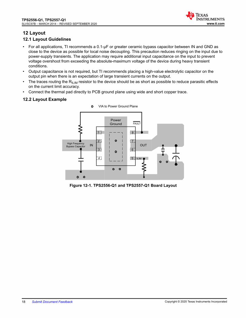
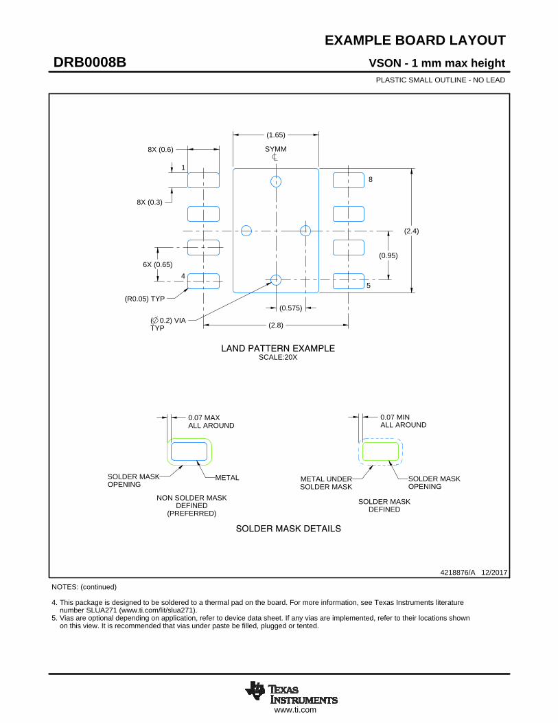
12 Layout12.1 Layout Guidelines• For all applications, TI recommends a 0.1-µF or greater ceramic bypass capacitor between IN and GND as
close to the device as possible for local noise decoupling. This precaution reduces ringing on the input due topower-supply transients. The application may require additional input capacitance on the input to preventvoltage overshoot from exceeding the absolute-maximum voltage of the device during heavy transientconditions.
• Output capacitance is not required, but TI recommends placing a high-value electrolytic capacitor on theoutput pin when there is an expectation of large transient currents on the output.
• The traces routing the RILIM resistor to the device should be as short as possible to reduce parasitic effectson the current limit accuracy.
• Connect the thermal pad directly to PCB ground plane using wide and short copper trace.
12.2 Layout Example
Power
Ground
1
2
3
4
6
5
7
8
OUTINHigh Frequency
Bypass Capacitor
VIA to Power Ground Plane
FAULT
ILIM
Figure 12-1. TPS2556-Q1 and TPS2557-Q1 Board Layout
TPS2556-Q1, TPS2557-Q1SLVSC97B – MARCH 2014 – REVISED SEPTEMBER 2020 www.ti.com
18 Submit Document Feedback Copyright © 2020 Texas Instruments Incorporated
13 Device and Documentation Support13.1 Related LinksThe following table lists quick access links. Categories include technical documents, support and communityresources, tools and software, and quick access to sample or buy.
Table 13-1. Related LinksPARTS PRODUCT FOLDER SAMPLE & BUY TECHNICAL
DOCUMENTSTOOLS &
SOFTWARESUPPORT &COMMUNITY
TPS2556-Q1 Click here Click here Click here Click here Click here
TPS2557-Q1 Click here Click here Click here Click here Click here
13.2 TrademarksAll other trademarks are the property of their respective owners.13.3 Electrostatic Discharge Caution
This integrated circuit can be damaged by ESD. Texas Instruments recommends that all integrated circuits be handledwith appropriate precautions. Failure to observe proper handling and installation procedures can cause damage.ESD damage can range from subtle performance degradation to complete device failure. Precision integrated circuits maybe more susceptible to damage because very small parametric changes could cause the device not to meet its publishedspecifications.
13.4 GlossaryTI Glossary This glossary lists and explains terms, acronyms, and definitions.
www.ti.comTPS2556-Q1, TPS2557-Q1
SLVSC97B – MARCH 2014 – REVISED SEPTEMBER 2020
Copyright © 2020 Texas Instruments Incorporated Submit Document Feedback 19
14 Mechanical, Packaging, and Orderable InformationThe following packaging information and addendum reflect the most-current data available for the designateddevices. This data is subject to change without notice and without revision of this document.
TPS2556-Q1, TPS2557-Q1SLVSC97B – MARCH 2014 – REVISED SEPTEMBER 2020 www.ti.com
20 Submit Document Feedback Copyright © 2020 Texas Instruments Incorporated
PACKAGE OPTION ADDENDUM
www.ti.com 10-Dec-2020
Addendum-Page 1
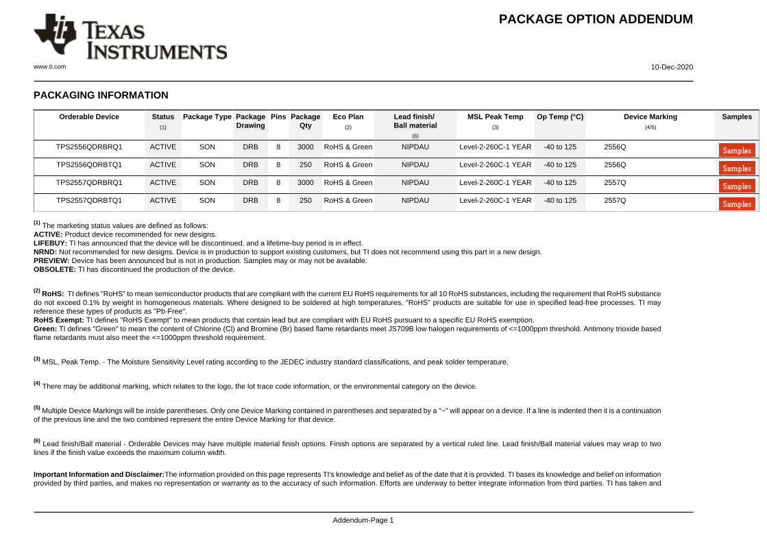
PACKAGING INFORMATION
Orderable Device Status(1)
Package Type PackageDrawing
Pins PackageQty
Eco Plan(2)
Lead finish/Ball material
(6)
MSL Peak Temp(3)
Op Temp (°C) Device Marking(4/5)
Samples
TPS2556QDRBRQ1 ACTIVE SON DRB 8 3000 RoHS & Green NIPDAU Level-2-260C-1 YEAR -40 to 125 2556Q
TPS2556QDRBTQ1 ACTIVE SON DRB 8 250 RoHS & Green NIPDAU Level-2-260C-1 YEAR -40 to 125 2556Q
TPS2557QDRBRQ1 ACTIVE SON DRB 8 3000 RoHS & Green NIPDAU Level-2-260C-1 YEAR -40 to 125 2557Q
TPS2557QDRBTQ1 ACTIVE SON DRB 8 250 RoHS & Green NIPDAU Level-2-260C-1 YEAR -40 to 125 2557Q
(1) The marketing status values are defined as follows:ACTIVE: Product device recommended for new designs.LIFEBUY: TI has announced that the device will be discontinued, and a lifetime-buy period is in effect.NRND: Not recommended for new designs. Device is in production to support existing customers, but TI does not recommend using this part in a new design.PREVIEW: Device has been announced but is not in production. Samples may or may not be available.OBSOLETE: TI has discontinued the production of the device.
(2) RoHS: TI defines "RoHS" to mean semiconductor products that are compliant with the current EU RoHS requirements for all 10 RoHS substances, including the requirement that RoHS substancedo not exceed 0.1% by weight in homogeneous materials. Where designed to be soldered at high temperatures, "RoHS" products are suitable for use in specified lead-free processes. TI mayreference these types of products as "Pb-Free".RoHS Exempt: TI defines "RoHS Exempt" to mean products that contain lead but are compliant with EU RoHS pursuant to a specific EU RoHS exemption.Green: TI defines "Green" to mean the content of Chlorine (Cl) and Bromine (Br) based flame retardants meet JS709B low halogen requirements of <=1000ppm threshold. Antimony trioxide basedflame retardants must also meet the <=1000ppm threshold requirement.
(3) MSL, Peak Temp. - The Moisture Sensitivity Level rating according to the JEDEC industry standard classifications, and peak solder temperature.
(4) There may be additional marking, which relates to the logo, the lot trace code information, or the environmental category on the device.
(5) Multiple Device Markings will be inside parentheses. Only one Device Marking contained in parentheses and separated by a "~" will appear on a device. If a line is indented then it is a continuationof the previous line and the two combined represent the entire Device Marking for that device.
(6) Lead finish/Ball material - Orderable Devices may have multiple material finish options. Finish options are separated by a vertical ruled line. Lead finish/Ball material values may wrap to twolines if the finish value exceeds the maximum column width.
Important Information and Disclaimer:The information provided on this page represents TI's knowledge and belief as of the date that it is provided. TI bases its knowledge and belief on informationprovided by third parties, and makes no representation or warranty as to the accuracy of such information. Efforts are underway to better integrate information from third parties. TI has taken and
PACKAGE OPTION ADDENDUM
www.ti.com 10-Dec-2020
Addendum-Page 2
continues to take reasonable steps to provide representative and accurate information but may not have conducted destructive testing or chemical analysis on incoming materials and chemicals.TI and TI suppliers consider certain information to be proprietary, and thus CAS numbers and other limited information may not be available for release.
In no event shall TI's liability arising out of such information exceed the total purchase price of the TI part(s) at issue in this document sold by TI to Customer on an annual basis.
OTHER QUALIFIED VERSIONS OF TPS2556-Q1, TPS2557-Q1 :
• Catalog: TPS2556, TPS2557
NOTE: Qualified Version Definitions:
• Catalog - TI's standard catalog product
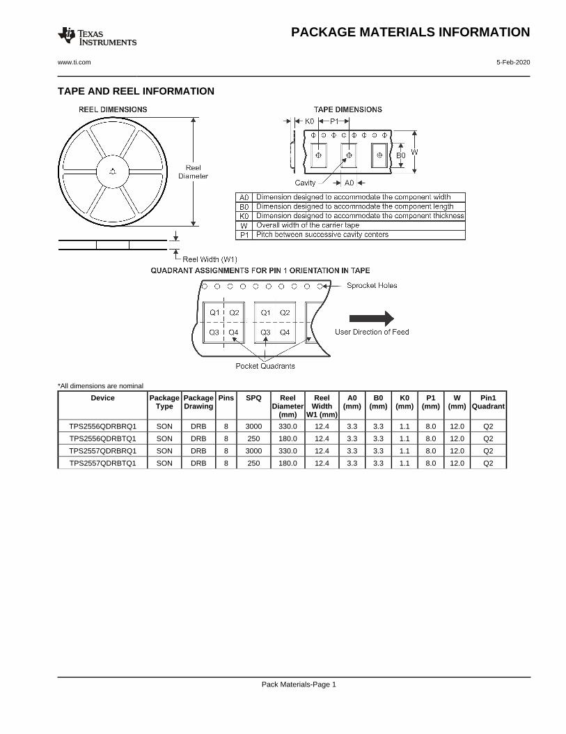
TAPE AND REEL INFORMATION
*All dimensions are nominal
Device PackageType
PackageDrawing
Pins SPQ ReelDiameter
(mm)
ReelWidth
W1 (mm)
A0(mm)
B0(mm)
K0(mm)
P1(mm)
W(mm)
Pin1Quadrant
TPS2556QDRBRQ1 SON DRB 8 3000 330.0 12.4 3.3 3.3 1.1 8.0 12.0 Q2
TPS2556QDRBTQ1 SON DRB 8 250 180.0 12.4 3.3 3.3 1.1 8.0 12.0 Q2
TPS2557QDRBRQ1 SON DRB 8 3000 330.0 12.4 3.3 3.3 1.1 8.0 12.0 Q2
TPS2557QDRBTQ1 SON DRB 8 250 180.0 12.4 3.3 3.3 1.1 8.0 12.0 Q2
PACKAGE MATERIALS INFORMATION
www.ti.com 5-Feb-2020
Pack Materials-Page 1
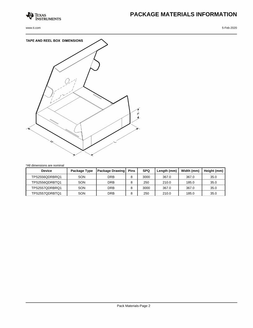
*All dimensions are nominal
Device Package Type Package Drawing Pins SPQ Length (mm) Width (mm) Height (mm)
TPS2556QDRBRQ1 SON DRB 8 3000 367.0 367.0 35.0
TPS2556QDRBTQ1 SON DRB 8 250 210.0 185.0 35.0
TPS2557QDRBRQ1 SON DRB 8 3000 367.0 367.0 35.0
TPS2557QDRBTQ1 SON DRB 8 250 210.0 185.0 35.0
PACKAGE MATERIALS INFORMATION
www.ti.com 5-Feb-2020
Pack Materials-Page 2
www.ti.com
PACKAGE OUTLINE
C
8X 0.350.25
2.4 0.052X
1.95
1.65 0.05
6X 0.65
1 MAX
8X 0.50.3
0.050.00
A 3.12.9
B
3.12.9
(0.2) TYP
VSON - 1 mm max heightDRB0008BPLASTIC SMALL OUTLINE - NO LEAD
4218876/A 12/2017
PIN 1 INDEX AREA
SEATING PLANE
0.08 C
1
4 5
8
(OPTIONAL)PIN 1 ID 0.1 C A B
0.05 C
THERMAL PADEXPOSED
NOTES: 1. All linear dimensions are in millimeters. Any dimensions in parenthesis are for reference only. Dimensioning and tolerancing per ASME Y14.5M. 2. This drawing is subject to change without notice. 3. The package thermal pad must be soldered to the printed circuit board for thermal and mechanical performance.
SCALE 4.000
www.ti.com
EXAMPLE BOARD LAYOUT
0.07 MINALL AROUND
0.07 MAXALL AROUND
8X (0.3)
(2.4)
(2.8)
6X (0.65)
(1.65)
( 0.2) VIATYP
(0.575)
(0.95)
8X (0.6)
(R0.05) TYP
VSON - 1 mm max heightDRB0008BPLASTIC SMALL OUTLINE - NO LEAD
4218876/A 12/2017
SYMM
1
45
8
LAND PATTERN EXAMPLESCALE:20X
NOTES: (continued) 4. This package is designed to be soldered to a thermal pad on the board. For more information, see Texas Instruments literature number SLUA271 (www.ti.com/lit/slua271).5. Vias are optional depending on application, refer to device data sheet. If any vias are implemented, refer to their locations shown on this view. It is recommended that vias under paste be filled, plugged or tented.
SOLDER MASKOPENINGSOLDER MASK
METAL UNDER
SOLDER MASKDEFINED
METALSOLDER MASKOPENING
SOLDER MASK DETAILS
NON SOLDER MASKDEFINED
(PREFERRED)
www.ti.com
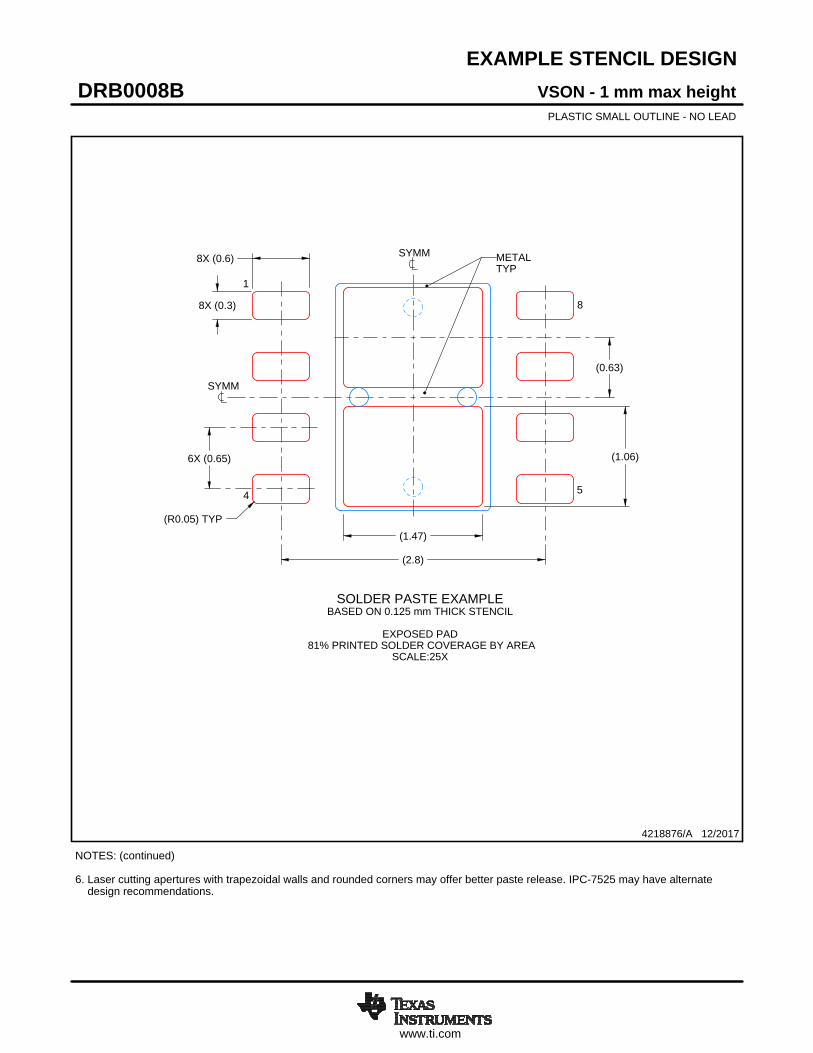
EXAMPLE STENCIL DESIGN
(R0.05) TYP
8X (0.3)
8X (0.6)
(1.47)
(1.06)
(2.8)
(0.63)
6X (0.65)
VSON - 1 mm max heightDRB0008BPLASTIC SMALL OUTLINE - NO LEAD
4218876/A 12/2017
NOTES: (continued) 6. Laser cutting apertures with trapezoidal walls and rounded corners may offer better paste release. IPC-7525 may have alternate design recommendations.
SOLDER PASTE EXAMPLEBASED ON 0.125 mm THICK STENCIL
EXPOSED PAD
81% PRINTED SOLDER COVERAGE BY AREASCALE:25X
SYMM
1
4 5
8
METALTYP
SYMM
IMPORTANT NOTICE AND DISCLAIMER
TI PROVIDES TECHNICAL AND RELIABILITY DATA (INCLUDING DATASHEETS), DESIGN RESOURCES (INCLUDING REFERENCE DESIGNS), APPLICATION OR OTHER DESIGN ADVICE, WEB TOOLS, SAFETY INFORMATION, AND OTHER RESOURCES “AS IS” AND WITH ALL FAULTS, AND DISCLAIMS ALL WARRANTIES, EXPRESS AND IMPLIED, INCLUDING WITHOUT LIMITATION ANY IMPLIED WARRANTIES OF MERCHANTABILITY, FITNESS FOR A PARTICULAR PURPOSE OR NON-INFRINGEMENT OF THIRD PARTY INTELLECTUAL PROPERTY RIGHTS.These resources are intended for skilled developers designing with TI products. You are solely responsible for (1) selecting the appropriate TI products for your application, (2) designing, validating and testing your application, and (3) ensuring your application meets applicable standards, and any other safety, security, or other requirements. These resources are subject to change without notice. TI grants you permission to use these resources only for development of an application that uses the TI products described in the resource. Other reproduction and display of these resources is prohibited. No license is granted to any other TI intellectual property right or to any third party intellectual property right. TI disclaims responsibility for, and you will fully indemnify TI and its representatives against, any claims, damages, costs, losses, and liabilities arising out of your use of these resources.TI’s products are provided subject to TI’s Terms of Sale (www.ti.com/legal/termsofsale.html) or other applicable terms available either on ti.com or provided in conjunction with such TI products. TI’s provision of these resources does not expand or otherwise alter TI’s applicable warranties or warranty disclaimers for TI products.
Mailing Address: Texas Instruments, Post Office Box 655303, Dallas, Texas 75265Copyright © 2020, Texas Instruments Incorporated