Embed Size (px)
Citation preview
IN
EN
SS
PG
OUT
SNSCSS
CIN
COUT
1.5 V
GND
1.2 V = 0.5 V
+ 100 mV+ 200 mV+ 400 mV
ref
TPS7A7200
FB
1.6V
800mV400mV200mV
100mV
50mV
Optional
CFF
0
1
2
3
4
5
6
1.5V to 1.0V1.5V to 1.2V
1.8V to 1.5V
2.5V to 1.8V
3.0V to 2.5V
3.3V to 3.0V
5.5V to 5.0V
0
1
2
3
Time (100µs/div)
Out
put V
olta
ge (
V)
Out
put C
urre
nt (
A)Output Current
Output Current Slew Rate: 1A/µs
G311
Product
Folder
Sample &Buy
Technical
Documents
Tools &
Software
Support &Community
An IMPORTANT NOTICE at the end of this data sheet addresses availability, warranty, changes, use in safety-critical applications,intellectual property matters and other important disclaimers. PRODUCTION DATA.
TPS7A7200SBVS136F –MARCH 2012–REVISED NOVEMBER 2015
TPS7A7200 2-A, Fast-Transient, Low-Dropout Voltage Regulator
1
1 Features1• Low-Dropout Voltage: 180 mV at 2 A• VIN Range: 1.5 V to 6.5 V• Configurable Fixed VOUT Range: 0.9 V to 3.5 V• Adjustable VOUT Range: 0.9 V to 5 V• Very Good Load- and Line-Transient Response• Stable With Ceramic Output Capacitor• 1.5% Accuracy Overline, Overload, and
Overtemperature• Programmable Soft Start• Power Good (PG) Output• 3-mm × 3-mm QFN-16 and 5-mm × 5-mm
VQFN-20 Packages
2 Applications• Wireless Infrastructure: SerDes, FPGA, DSP™• RF Components: VCO, ADC, DAC, LVDS• Set-Top Boxes: Amplifier, ADC, DAC, FPGA, DSP• Wireless LAN, Bluetooth®
• PCs and Printers• Audio and Visual
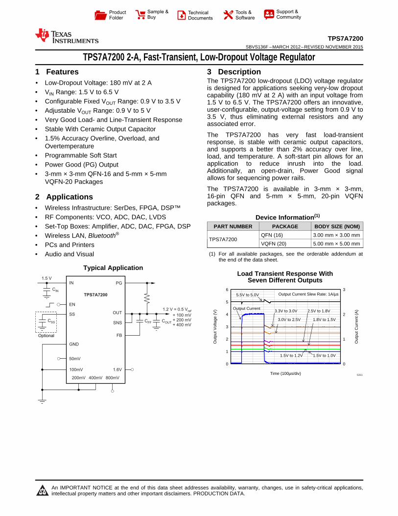
3 DescriptionThe TPS7A7200 low-dropout (LDO) voltage regulatoris designed for applications seeking very-low dropoutcapability (180 mV at 2 A) with an input voltage from1.5 V to 6.5 V. The TPS7A7200 offers an innovative,user-configurable, output-voltage setting from 0.9 V to3.5 V, thus eliminating external resistors and anyassociated error.
The TPS7A7200 has very fast load-transientresponse, is stable with ceramic output capacitors,and supports a better than 2% accuracy over line,load, and temperature. A soft-start pin allows for anapplication to reduce inrush into the load.Additionally, an open-drain, Power Good signalallows for sequencing power rails.
The TPS7A7200 is available in 3-mm × 3-mm,16-pin QFN and 5-mm × 5-mm, 20-pin VQFNpackages.
Device Information(1)
PART NUMBER PACKAGE BODY SIZE (NOM)
TPS7A7200QFN (16) 3.00 mm × 3.00 mmVQFN (20) 5.00 mm × 5.00 mm
(1) For all available packages, see the orderable addendum atthe end of the data sheet.
Typical ApplicationLoad Transient Response With
Seven Different Outputs
2
TPS7A7200SBVS136F –MARCH 2012–REVISED NOVEMBER 2015 www.ti.com
Product Folder Links: TPS7A7200
Submit Documentation Feedback Copyright © 2012–2015, Texas Instruments Incorporated
Table of Contents1 Features .................................................................. 12 Applications ........................................................... 13 Description ............................................................. 14 Revision History..................................................... 25 Pin Configurations................................................. 46 Specifications......................................................... 5
6.1 Absolute Maximum Ratings ..................................... 56.2 ESD Ratings.............................................................. 56.3 Recommended Operating Conditions....................... 56.4 Thermal Information .................................................. 66.5 Electrical Characteristics........................................... 76.6 Typical Characteristics .............................................. 8
7 Detailed Description ............................................ 127.1 Overview ................................................................. 127.2 Functional Block Diagram ....................................... 127.3 Feature Description................................................. 137.4 Device Functional Modes........................................ 22
8 Application and Implementation ........................ 238.1 Application Information............................................ 238.2 Typical Application .................................................. 23
9 Power Supply Recommendations ...................... 2710 Layout................................................................... 27
10.1 Layout Guidelines ................................................. 2710.2 Layout Example .................................................... 2710.3 Thermal Considerations ........................................ 2810.4 Power Dissipation ................................................. 2810.5 Estimating Junction Temperature ........................ 29
11 Device And Documentation Support................. 3111.1 Documentation Support ........................................ 3111.2 Community Resources.......................................... 3111.3 Trademarks ........................................................... 3111.4 Electrostatic Discharge Caution............................ 3111.5 Glossary ................................................................ 31
12 Mechanical, Packaging, And OrderableInformation ........................................................... 31
4 Revision HistoryNOTE: Page numbers for previous revisions may differ from page numbers in the current version.
Changes from Revision E (September 2013) to Revision F Page
• Added ESD Ratings table, Feature Description section, Device Functional Modes, Application and Implementationsection, Power Supply Recommendations section, Layout section, Device and Documentation Support section, andMechanical, Packaging, and Orderable Information section. ................................................................................................ 1
• Changed name of section from Enable and Shutdown the Device to Enable ..................................................................... 21
Changes from Revision C (May 2012) to Revision D Page
• Added CFF capacitor to front page block diagram .................................................................................................................. 1• Added text to FB pin description ............................................................................................................................................ 4• Added CFF test condition and table note to Electrical Characteristics.................................................................................... 7• Deleted maximum value for Output Current Limit parameter in Electrical Characteristics table ........................................... 7• Added CFF capacitor to Figure 24......................................................................................................................................... 13• Added CFF capacitor to Figure 25......................................................................................................................................... 14• Added CFF capacitor to Figure 26......................................................................................................................................... 15• Added CFF capacitor to Figure 27......................................................................................................................................... 16• Added CFF capacitor to Figure 28......................................................................................................................................... 17• Added CFF capacitor to Figure 29......................................................................................................................................... 18• Added CFF capacitor to Figure 30......................................................................................................................................... 20• Changed capacitor values in first sentence of Output Capacitor Requirements section ..................................................... 24
3
TPS7A7200www.ti.com SBVS136F –MARCH 2012–REVISED NOVEMBER 2015
Product Folder Links: TPS7A7200
Submit Documentation FeedbackCopyright © 2012–2015, Texas Instruments Incorporated
Changes from Revision B (April 2012) to Revision C Page
• Added RGT package to Figure 44 ....................................................................................................................................... 28• Added RGT package to Figure 46 ....................................................................................................................................... 30
Changes from Revision A (March 2012) to Revision B Page
• Changed Accuracy feature bullet ........................................................................................................................................... 1• Added RGT (QFN-16) package to Features .......................................................................................................................... 1• Added RGT package pinout drawing...................................................................................................................................... 4• Added RGT package to Pin Descriptions table ...................................................................................................................... 4• Added RGT (QFN-16) package to Thermal Information table................................................................................................ 6• Added test conditions for RGT package to Output Voltage Accuracy parameter .................................................................. 7
Changes from Original (March 2012) to Revision A Page
• Changed from product preview to production data ................................................................................................................ 1
OUT
SNS
FB
PG
50mV
IN
EN
SS
NC
1.6V
OU
T100m
V6
200m
V7
GN
D8
400m
V9
800m
V10
1
2
3
4
5
15
14
13
12
11
20
OU
T19
18
IN17
IN16
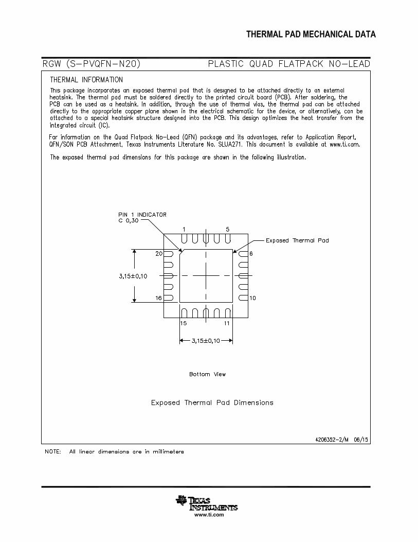
Thermal Pad
GN
D
100m
V5
200m
V6
GN
D7
400m
V8
SNS
FB
PG
50mV
1
2
3
4
EN
SS
1.6V
800mV
12
11
10
9
Thermal Pad
OU
T16
OU
T15
14
IN13
IN
4
TPS7A7200SBVS136F –MARCH 2012–REVISED NOVEMBER 2015 www.ti.com
Product Folder Links: TPS7A7200
Submit Documentation Feedback Copyright © 2012–2015, Texas Instruments Incorporated
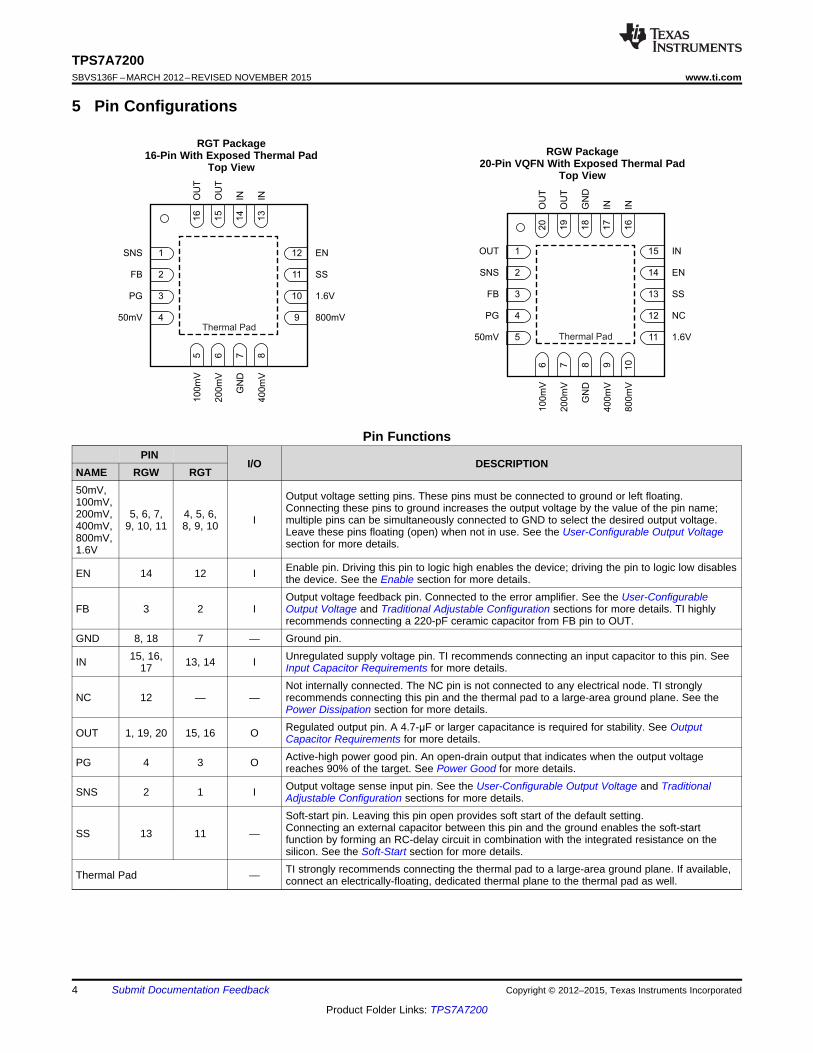
5 Pin Configurations
RGT Package16-Pin With Exposed Thermal Pad
Top ViewRGW Package
20-Pin VQFN With Exposed Thermal PadTop View
Pin FunctionsPIN
I/O DESCRIPTIONNAME RGW RGT50mV,100mV,200mV,400mV,800mV,1.6V
5, 6, 7,9, 10, 11
4, 5, 6,8, 9, 10 I
Output voltage setting pins. These pins must be connected to ground or left floating.Connecting these pins to ground increases the output voltage by the value of the pin name;multiple pins can be simultaneously connected to GND to select the desired output voltage.Leave these pins floating (open) when not in use. See the User-Configurable Output Voltagesection for more details.
EN 14 12 I Enable pin. Driving this pin to logic high enables the device; driving the pin to logic low disablesthe device. See the Enable section for more details.
FB 3 2 IOutput voltage feedback pin. Connected to the error amplifier. See the User-ConfigurableOutput Voltage and Traditional Adjustable Configuration sections for more details. TI highlyrecommends connecting a 220-pF ceramic capacitor from FB pin to OUT.
GND 8, 18 7 — Ground pin.
IN 15, 16,17 13, 14 I Unregulated supply voltage pin. TI recommends connecting an input capacitor to this pin. See
Input Capacitor Requirements for more details.
NC 12 — —Not internally connected. The NC pin is not connected to any electrical node. TI stronglyrecommends connecting this pin and the thermal pad to a large-area ground plane. See thePower Dissipation section for more details.
OUT 1, 19, 20 15, 16 O Regulated output pin. A 4.7-μF or larger capacitance is required for stability. See OutputCapacitor Requirements for more details.
PG 4 3 O Active-high power good pin. An open-drain output that indicates when the output voltagereaches 90% of the target. See Power Good for more details.
SNS 2 1 I Output voltage sense input pin. See the User-Configurable Output Voltage and TraditionalAdjustable Configuration sections for more details.
SS 13 11 —
Soft-start pin. Leaving this pin open provides soft start of the default setting.Connecting an external capacitor between this pin and the ground enables the soft-startfunction by forming an RC-delay circuit in combination with the integrated resistance on thesilicon. See the Soft-Start section for more details.
Thermal Pad — TI strongly recommends connecting the thermal pad to a large-area ground plane. If available,connect an electrically-floating, dedicated thermal plane to the thermal pad as well.
5
TPS7A7200www.ti.com SBVS136F –MARCH 2012–REVISED NOVEMBER 2015
Product Folder Links: TPS7A7200
Submit Documentation FeedbackCopyright © 2012–2015, Texas Instruments Incorporated
(1) Stresses beyond those listed under Absolute Maximum Ratings may cause permanent damage to the device. These are stress ratingsonly, and functional operation of the device at these or any other conditions beyond those indicated is not implied. Exposure to absolute-maximum-rated conditions for extended periods may affect device reliability.
(2) The absolute maximum rating is VIN + 0.3 V or +7 V, whichever is smaller.
6 Specifications
6.1 Absolute Maximum RatingsOver operating junction temperature range (unless otherwise noted). (1)
MIN MAX UNIT
VoltageIN, PG, EN –0.3 7 VSS, FB, SNS, OUT –0.3 VIN + 0.3 (2) V50 mV, 100 mV, 200 mV, 400 mV, 800 mV, 1.6 V –0.3 VOUT + 0.3 (2) V
CurrentOUT Internally limited APG (sink current into IC) 5 mA
TemperatureOperating virtual junction, TJ –55 160 °CStorage, Tstg –55 150 °C
(1) JEDEC document JEP155 states that 500-V HBM allows safe manufacturing with a standard ESD control process.(2) JEDEC document JEP157 states that 250-V CDM allows safe manufacturing with a standard ESD control process.
6.2 ESD RatingsVALUE UNIT
V(ESD) Electrostatic dischargeHuman-body model (HBM), per ANSI/ESDA/JEDEC JS-001 (1) ±2000
VCharged-device model (CDM), per JEDEC specification JESD22-C101 (2) ±500
(1) For output capacitors larger than 47 µF, a feedforward capacitor of at least 220 pF must be used.
6.3 Recommended Operating Conditionsover operating junction temperature range (unless otherwise noted)
MIN NOM MAX UNITVIN Supply voltage 1.425 6.5 VVOUT Output voltage 0.9 5 VVEN Enable voltage 0 6.5 VVPG Pullup voltage 0 6.5 V
Any-out voltage 50 mV, 100 mV, 200 mV,400 mV, 800 mV, 1.6 V 0 VOUT V
IOUT Output current 0 2 ACOUT Output capacitance 4.7 200 (1) µFCF Feedforward capacitance 0 100 nFTJ Junction temperature –40 125 °C
6
TPS7A7200SBVS136F –MARCH 2012–REVISED NOVEMBER 2015 www.ti.com
Product Folder Links: TPS7A7200
Submit Documentation Feedback Copyright © 2012–2015, Texas Instruments Incorporated
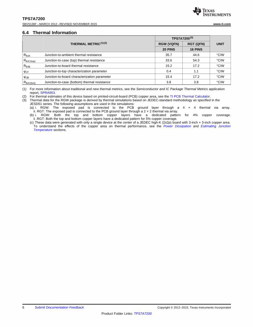
(1) For more information about traditional and new thermal metrics, see the Semiconductor and IC Package Thermal Metrics applicationreport, SPRA953.
(2) For thermal estimates of this device based on printed-circuit-board (PCB) copper area, see the TI PCB Thermal Calculator.(3) Thermal data for the RGW package is derived by thermal simulations based on JEDEC-standard methodology as specified in the
JESD51 series. The following assumptions are used in the simulations:(a) i. RGW: The exposed pad is connected to the PCB ground layer through a 4 × 4 thermal via array.
ii. RGT: The exposed pad is connected to the PCB ground layer through a 2 × 2 thermal via array.(b) i. RGW: Both the top and bottom copper layers have a dedicated pattern for 4% copper coverage.
ii .RGT: Both the top and bottom copper layers have a dedicated pattern for 5% copper coverage.(c) These data were generated with only a single device at the center of a JEDEC high-K (2s2p) board with 3-inch × 3-inch copper area.
To understand the effects of the copper area on thermal performance, see the Power Dissipation and Estimating JunctionTemperature sections.
6.4 Thermal Information
THERMAL METRIC (1) (2)TPS7A7200 (3)
UNITRGW (VQFN) RGT (QFN)20 PINS 16 PINS
RθJA Junction-to-ambient thermal resistance 35.7 44.6 °C/WRθJC(top) Junction-to-case (top) thermal resistance 33.6 54.3 °C/WRθJB Junction-to-board thermal resistance 15.2 17.2 °C/WψJT Junction-to-top characterization parameter 0.4 1.1 °C/WψJB Junction-to-board characterization parameter 15.4 17.2 °C/WRθJC(bot) Junction-to-case (bottom) thermal resistance 3.8 3.8 °C/W
7
TPS7A7200www.ti.com SBVS136F –MARCH 2012–REVISED NOVEMBER 2015
Product Folder Links: TPS7A7200
Submit Documentation FeedbackCopyright © 2012–2015, Texas Instruments Incorporated
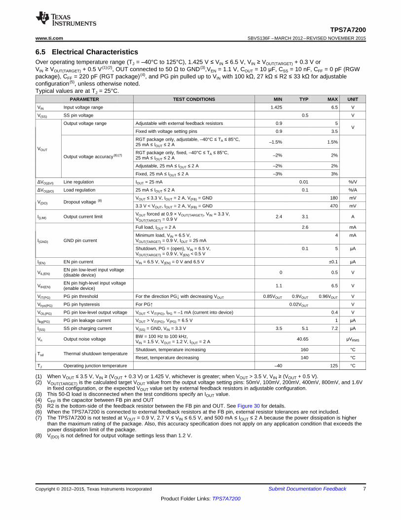
(1) When VOUT ≤ 3.5 V, VIN ≥ (VOUT + 0.3 V) or 1.425 V, whichever is greater; when VOUT > 3.5 V, VIN ≥ (VOUT + 0.5 V).(2) VOUT(TARGET) is the calculated target VOUT value from the output voltage setting pins: 50mV, 100mV, 200mV, 400mV, 800mV, and 1.6V
in fixed configuration, or the expected VOUT value set by external feedback resistors in adjustable configuration.(3) This 50-Ω load is disconnected when the test conditions specify an IOUT value.(4) CFF is the capacitor between FB pin and OUT(5) R2 is the bottom-side of the feedback resistor between the FB pin and OUT. See Figure 30 for details.(6) When the TPS7A7200 is connected to external feedback resistors at the FB pin, external resistor tolerances are not included.(7) The TPS7A7200 is not tested at VOUT = 0.9 V, 2.7 V ≤ VIN ≤ 6.5 V, and 500 mA ≤ IOUT ≤ 2 A because the power dissipation is higher
than the maximum rating of the package. Also, this accuracy specification does not apply on any application condition that exceeds thepower dissipation limit of the package.
(8) V(DO) is not defined for output voltage settings less than 1.2 V.
6.5 Electrical CharacteristicsOver operating temperature range (TJ = –40°C to 125°C), 1.425 V ≤ VIN ≤ 6.5 V, VIN ≥ VOUT(TARGET) + 0.3 V orVIN ≥ VOUT(TARGET) + 0.5 V (1) (2), OUT connected to 50 Ω to GND (3),VEN = 1.1 V, COUT = 10 μF, CSS = 10 nF, CFF = 0 pF (RGWpackage), CFF = 220 pF (RGT package) (4), and PG pin pulled up to VIN with 100 kΩ, 27 kΩ ≤ R2 ≤ 33 kΩ for adjustableconfiguration (5), unless otherwise noted.Typical values are at TJ = 25°C.
PARAMETER TEST CONDITIONS MIN TYP MAX UNIT
VIN Input voltage range 1.425 6.5 V
V(SS) SS pin voltage 0.5 V
VOUT
Output voltage range Adjustable with external feedback resistors 0.9 5V
Fixed with voltage setting pins 0.9 3.5
Output voltage accuracy (6) (7)
RGT package only, adjustable, –40°C ≤ TA ≤ 85°C,25 mA ≤ IOUT ≤ 2 A –1.5% 1.5%
RGT package only, fixed, –40°C ≤ TA ≤ 85°C,25 mA ≤ IOUT ≤ 2 A –2% 2%
Adjustable, 25 mA ≤ IOUT ≤ 2 A –2% 2%
Fixed, 25 mA ≤ IOUT ≤ 2 A –3% 3%
ΔVO(ΔVI) Line regulation IOUT = 25 mA 0.01 %/V
ΔVO(ΔIO) Load regulation 25 mA ≤ IOUT ≤ 2 A 0.1 %/A
V(DO) Dropout voltage (8) VOUT ≤ 3.3 V, IOUT = 2 A, V(FB) = GND 180 mV
3.3 V < VOUT, IOUT = 2 A, V(FB) = GND 470 mV
I(LIM) Output current limit VOUT forced at 0.9 × VOUT(TARGET), VIN = 3.3 V,VOUT(TARGET) = 0.9 V 2.4 3.1 A
I(GND) GND pin current
Full load, IOUT = 2 A 2.6 mA
Minimum load, VIN = 6.5 V,VOUT(TARGET) = 0.9 V, IOUT = 25 mA
4 mA
Shutdown, PG = (open), VIN = 6.5 V,VOUT(TARGET) = 0.9 V, V(EN) < 0.5 V
0.1 5 μA
I(EN) EN pin current VIN = 6.5 V, V(EN) = 0 V and 6.5 V ±0.1 μA
VIL(EN)EN pin low-level input voltage(disable device) 0 0.5 V
VIH(EN)EN pin high-level input voltage(enable device) 1.1 6.5 V
VIT(PG) PG pin threshold For the direction PG↓ with decreasing VOUT 0.85VOUT 0.9VOUT 0.96VOUT V
Vhys(PG) PG pin hysteresis For PG↑ 0.02VOUT V
VOL(PG) PG pin low-level output voltage VOUT < VIT(PG), IPG = –1 mA (current into device) 0.4 V
Ilkg(PG) PG pin leakage current VOUT > VIT(PG), V(PG) = 6.5 V 1 μA
I(SS) SS pin charging current V(SS) = GND, VIN = 3.3 V 3.5 5.1 7.2 μA
Vn Output noise voltage BW = 100 Hz to 100 kHz,VIN = 1.5 V, VOUT = 1.2 V, IOUT = 2 A 40.65 μVRMS
Tsd Thermal shutdown temperatureShutdown, temperature increasing 160 °C
Reset, temperature decreasing 140 °C
TJ Operating junction temperature –40 125 °C
0
50
100
150
200
250
300
0 0.5 1 1.5 2Output Current (A)
Dro
pout
Vol
tage
(m
V)
− 40°C0°C25°C85°C105°C125°C
VIN = 1.5 VFB = GND
G011
0
50
100
150
200
250
300
1 2 3 4 5 5.5Input Voltage (V)
Dro
pout
Vol
tage
(m
V)
− 40°C0°C25°C85°C105°C125°C
IOUT = 2 AFB = GND and plot VIN − VOUT
G014
0.873
0.882
0.891
0.9
0.909
0.918
0.927
0 0.5 1 1.5 2Output Current (A)
Out
put V
olta
ge (
V)
− 40°C0°C25°C85°C105°C125°C
Y−axis scale is 1%Vout/div
VIN = 1.425 VVOUT(TARGET) = 0.9 V400mV pin to GND; 50mV, 100mV200mV, 800mV, 1.6V pins open
G201
3.395
3.43
3.465
3.5
3.535
3.57
3.605
0 0.5 1 1.5 2Output Current (A)
Out
put V
olta
ge (
V)
− 40°C0°C25°C85°C105°C125°C
Y−axis scale is 1%Vout/div
VIN = 3.8 VVOUT(TARGET) = 3.5 V200mV, 400mV, 800mV, 1.6V pinsto GND; 50mV, 100mV pins open
G204
0.873
0.882
0.891
0.9
0.909
0.918
0.927
0 0.5 1 1.5 2Output Current (A)
Out
put V
olta
ge (
V)
− 40°C0°C25°C85°C105°C125°C
Y−axis scale is 1%Vout/div
VIN = 1.425 VR1 = 24.1 kΩ, R2 = 30.1 kΩ
G001
4.85
4.9
4.95
5
5.05
5.1
5.15
0 0.5 1 1.5 2Output Current (A)
Out
put V
olta
ge (
V)
− 40°C0°C25°C85°C105°C125°C
Y−axis scale is 1%Vout/div
VIN = 5.3 VR1 = 271 kΩ, R2 = 30.1 kΩ
G004
8
TPS7A7200SBVS136F –MARCH 2012–REVISED NOVEMBER 2015 www.ti.com
Product Folder Links: TPS7A7200
Submit Documentation Feedback Copyright © 2012–2015, Texas Instruments Incorporated
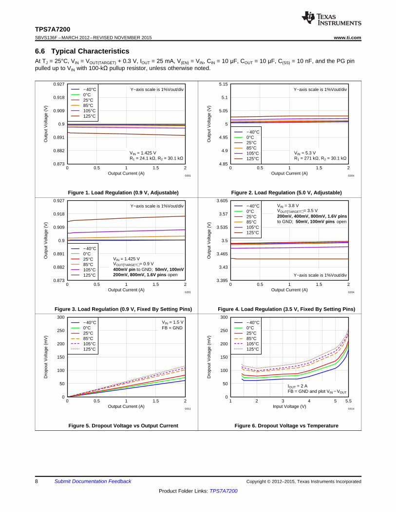
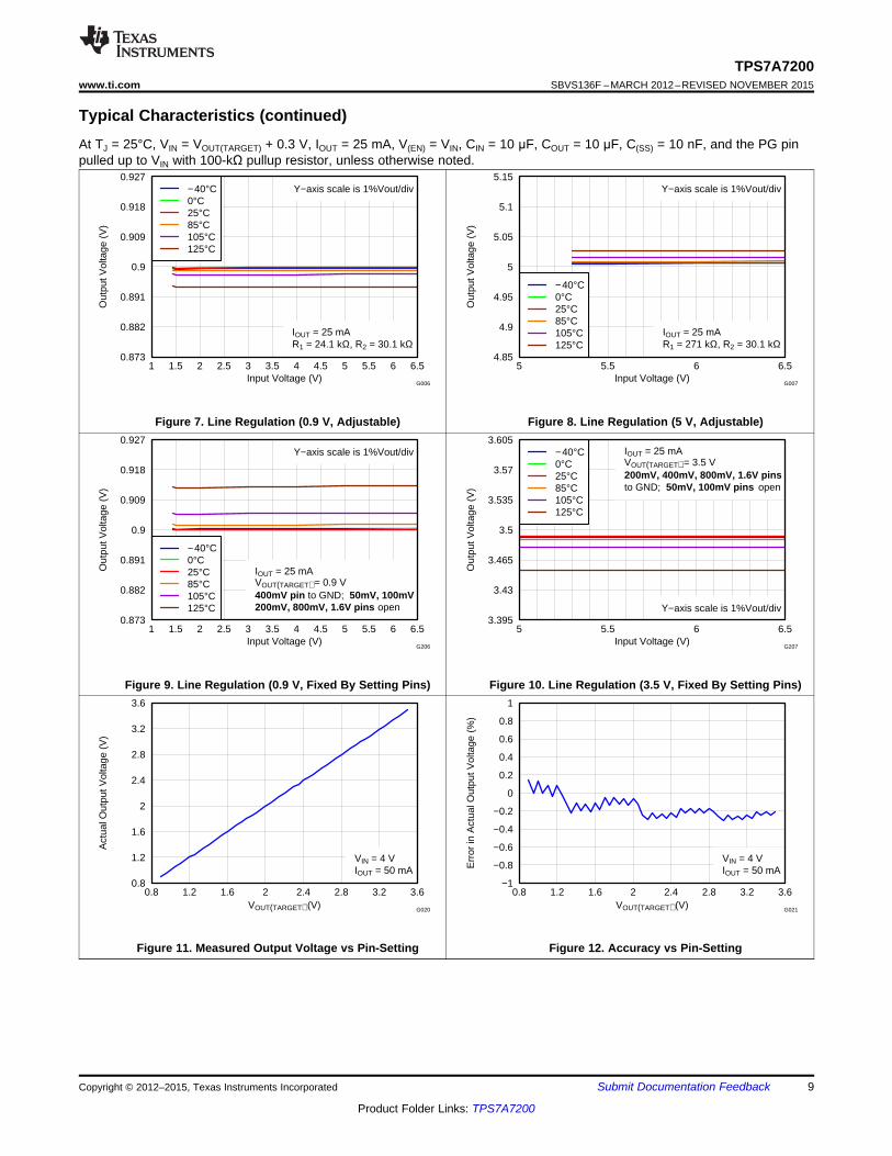
6.6 Typical CharacteristicsAt TJ = 25°C, VIN = VOUT(TARGET) + 0.3 V, IOUT = 25 mA, V(EN) = VIN, CIN = 10 μF, COUT = 10 μF, C(SS) = 10 nF, and the PG pinpulled up to VIN with 100-kΩ pullup resistor, unless otherwise noted.
Figure 1. Load Regulation (0.9 V, Adjustable) Figure 2. Load Regulation (5.0 V, Adjustable)
Figure 3. Load Regulation (0.9 V, Fixed By Setting Pins) Figure 4. Load Regulation (3.5 V, Fixed By Setting Pins)
Figure 5. Dropout Voltage vs Output Current Figure 6. Dropout Voltage vs Temperature
0.8
1.2
1.6
2
2.4
2.8
3.2
3.6
0.8 1.2 1.6 2 2.4 2.8 3.2 3.6VOUT(TARGET) (V)
Act
ual O
utpu
t Vol
tage
(V
)
VIN = 4 VIOUT = 50 mA
G020
−1
−0.8
−0.6
−0.4
−0.2
0
0.2
0.4
0.6
0.8
1
0.8 1.2 1.6 2 2.4 2.8 3.2 3.6VOUT(TARGET) (V)
Err
or in
Act
ual O
utpu
t Vol
tage
(%
)
VIN = 4 VIOUT = 50 mA
G021
0.873
0.882
0.891
0.9
0.909
0.918
0.927
1 1.5 2 2.5 3 3.5 4 4.5 5 5.5 6 6.5Input Voltage (V)
Out
put V
olta
ge (
V)
− 40°C0°C25°C85°C105°C125°C
Y−axis scale is 1%Vout/div
IOUT = 25 mAVOUT(TARGET) = 0.9 V400mV pin to GND; 50mV, 100mV200mV, 800mV, 1.6V pins open
G206
3.395
3.43
3.465
3.5
3.535
3.57
3.605
5 5.5 6 6.5Input Voltage (V)
Out
put V
olta
ge (
V)
− 40°C0°C25°C85°C105°C125°C
Y−axis scale is 1%Vout/div
IOUT = 25 mAVOUT(TARGET) = 3.5 V200mV, 400mV, 800mV, 1.6V pinsto GND; 50mV, 100mV pins open
G207
0.873
0.882
0.891
0.9
0.909
0.918
0.927
1 1.5 2 2.5 3 3.5 4 4.5 5 5.5 6 6.5Input Voltage (V)
Out
put V
olta
ge (
V)
− 40°C0°C25°C85°C105°C125°C
Y−axis scale is 1%Vout/div
IOUT = 25 mAR1 = 24.1 kΩ, R2 = 30.1 kΩ
G006
4.85
4.9
4.95
5
5.05
5.1
5.15
5 5.5 6 6.5Input Voltage (V)
Out
put V
olta
ge (
V)
− 40°C0°C25°C85°C105°C125°C
Y−axis scale is 1%Vout/div
IOUT = 25 mAR1 = 271 kΩ, R2 = 30.1 kΩ
G007
9
TPS7A7200www.ti.com SBVS136F –MARCH 2012–REVISED NOVEMBER 2015
Product Folder Links: TPS7A7200
Submit Documentation FeedbackCopyright © 2012–2015, Texas Instruments Incorporated
Typical Characteristics (continued)At TJ = 25°C, VIN = VOUT(TARGET) + 0.3 V, IOUT = 25 mA, V(EN) = VIN, CIN = 10 μF, COUT = 10 μF, C(SS) = 10 nF, and the PG pinpulled up to VIN with 100-kΩ pullup resistor, unless otherwise noted.
Figure 7. Line Regulation (0.9 V, Adjustable) Figure 8. Line Regulation (5 V, Adjustable)
Figure 9. Line Regulation (0.9 V, Fixed By Setting Pins) Figure 10. Line Regulation (3.5 V, Fixed By Setting Pins)
Figure 11. Measured Output Voltage vs Pin-Setting Figure 12. Accuracy vs Pin-Setting
84
85
86
87
88
89
90
91
92
93
94
95
96
−50 −25 0 25 50 75 100 125Temperature (°C)
Thr
esho
uld
Vol
tage
(%V
OU
T)
VIN=1.5VVIN=6.5V
VOUT(TARGET) = 1.2 V100mV, 200mV, 400mV pins to GND50mV, 800mV, 1.6V pins open50−Ω resistor between OUT and GND
G050
0
0.2
0.4
0.6
0.8
1
0 0.5 1 1.5 2Forced PG Pin Current (mA)
PG
Pin
Vol
tage
(V
)
VIN = 1.5 V, − 40 °CVIN = 1.5 V, 25 °CVIN = 1.5 V, 125 °CVIN = 6.5 V, − 40 °CVIN = 1.5 V, 25 °CVIN = 1.5 V, 125 °C
Spec limit defined at 1−mA.
VOUT(TARGET) = 1.2 V100mV, 200mV, 400mV pins to GND50mV, 800mV, 1.6V pins open50−Ω resistor from OUT to GND
G051
0
1
2
3
4
5
1 1.5 2 2.5 3 3.5 4 4.5 5 5.5 6 6.5Input Voltage (V)
Shu
tdow
n G
roun
d C
urre
nt (
µA)
− 40°C0°C25°C85°C105°C125°C
EN = GND50−Ω resistor between OUT and GND
G032
0
1
2
3
4
0 0.5 1 1.5 2 2.5 3 3.5Forced Output Voltage (V)
Cur
rent
Lim
it (A
)
VIN = 4 VVOUT(TARGET) = 3.5 V200mV, 400mV, 800mV, 1.6V pins to GND50mV, 100mV pins open
G041
0
1
2
3
4
5
0 0.5 1 1.5 2Output Current (A)
Gro
und
Cur
rent
(m
A)
− 40°C0°C25°C85°C105°C125°C
VIN = 1.8 VVOUT(TARGET) = 1.5 V200mV, 800mV pins to GND50mV, 100mV, 200mV, 400mV pins open
G030
0
1
2
3
4
5
1 1.5 2 2.5 3 3.5 4 4.5 5 5.5 6 6.5Input Voltage (V)
Gro
und
Cur
rent
(m
A)
− 40°C0°C25°C85°C105°C125°C
IOUT = 25 mAVOUT(TARGET) = 0.9 V400mV pin to GND; 50mV, 100mV200mV, 800mV, 1.6V pins open
G033
10
TPS7A7200SBVS136F –MARCH 2012–REVISED NOVEMBER 2015 www.ti.com
Product Folder Links: TPS7A7200
Submit Documentation Feedback Copyright © 2012–2015, Texas Instruments Incorporated
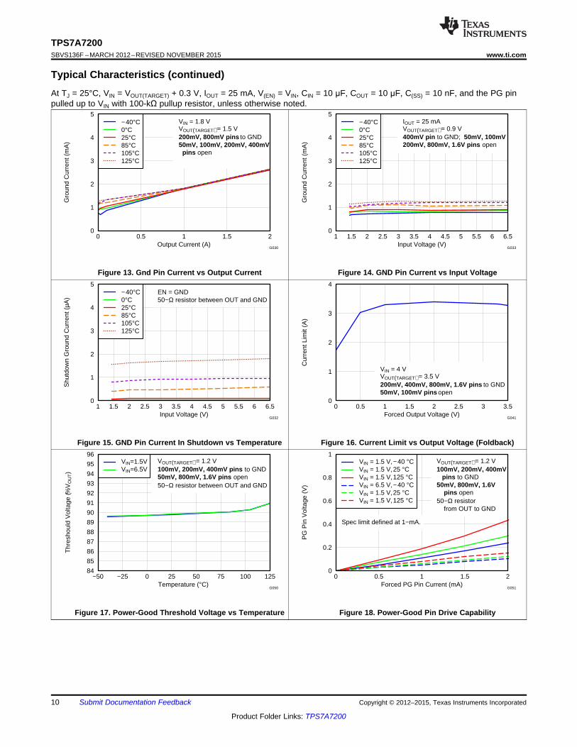
Typical Characteristics (continued)At TJ = 25°C, VIN = VOUT(TARGET) + 0.3 V, IOUT = 25 mA, V(EN) = VIN, CIN = 10 μF, COUT = 10 μF, C(SS) = 10 nF, and the PG pinpulled up to VIN with 100-kΩ pullup resistor, unless otherwise noted.
Figure 13. Gnd Pin Current vs Output Current Figure 14. GND Pin Current vs Input Voltage
Figure 15. GND Pin Current In Shutdown vs Temperature Figure 16. Current Limit vs Output Voltage (Foldback)
Figure 17. Power-Good Threshold Voltage vs Temperature Figure 18. Power-Good Pin Drive Capability
3.1
3.2
3.3
3.4
3.5
Output Voltage
0
2
4
6
8
Time (100µs/div)
Out
put V
olta
ge (
V)
Out
put C
urre
nt (
A)
OutputCurrent
Output Current Slew Rate: 1A/µsVOUT(TARGET)=3.3V400mV, 800mV, 1.6V pins to GND50mV, 100mV, 200mV pins open
G317
0
10
20
30
40
50
60
70
80
90
100
10 100 1k 10k 100k 1M 10MFrequency (Hz)
PS
RR
(dB
)
VIN=3.6V, IOUT=0.1AVIN=3.6V, IOUT=2AVIN=3.8V, IOUT=0.1AVIN=3.8V, IOUT=2A
VOUT(TARGET) = 3.3 V400mV, 800mV, 1.6V pins to GND50mV, 100mV, 200mV pins open
G071
1
1.1
1.2
1.3
1.4
Output Voltage
0
2
4
6
8
Time (100µs/div)
Out
put V
olta
ge (
V)
Out
put C
urre
nt (
A)
OutputCurrent
Output Current Slew Rate: 1A/µsVOUT(TARGET)=1.2V100mV, 200mV, 400mV pins to GND50mV, 800mV, 1.6V pins open
G314
0.01
0.1
1
10
10 100 1k 10k 100kFrequency (Hz)
Out
put S
pect
ral N
oise
Den
sity
(µV
/H
z)
VOUT(TARGET) = 0.9 VVOUT(TARGET) = 1.2 VVOUT(TARGET) = 3.3 V
VIN = VOUT(TARGET) + 0.3 VIOUT = 2 A100 Hz to 100 kHz RMS Noise 0.9 V: 37.43 µVRMS 1.2 V: 40.65 µVRMS 3.3 V: 82.59 µVRMS
G061
0.01
0.1
1
10
10 100 1k 10k 100kFrequency (Hz)
Out
put S
pect
ral N
oise
Den
sity
(µV
/H
z)
CSS = 100nF, COUT = 100µFCSS = 100nF, COUT = 10µFCSS = 10nF, COUT = 100µFCSS = 10nF, COUT = 10µFCSS = 1nF, COUT = 100µFCSS = 1nF, COUT = 10µF
VIN = 1.8 V, IOUT = 1 AVOUT(TARGET) = 1.5 V200mV, 800mV pins to GND50mV, 100mV, 400mV, 1.6V pins open
G063
11
TPS7A7200www.ti.com SBVS136F –MARCH 2012–REVISED NOVEMBER 2015
Product Folder Links: TPS7A7200
Submit Documentation FeedbackCopyright © 2012–2015, Texas Instruments Incorporated
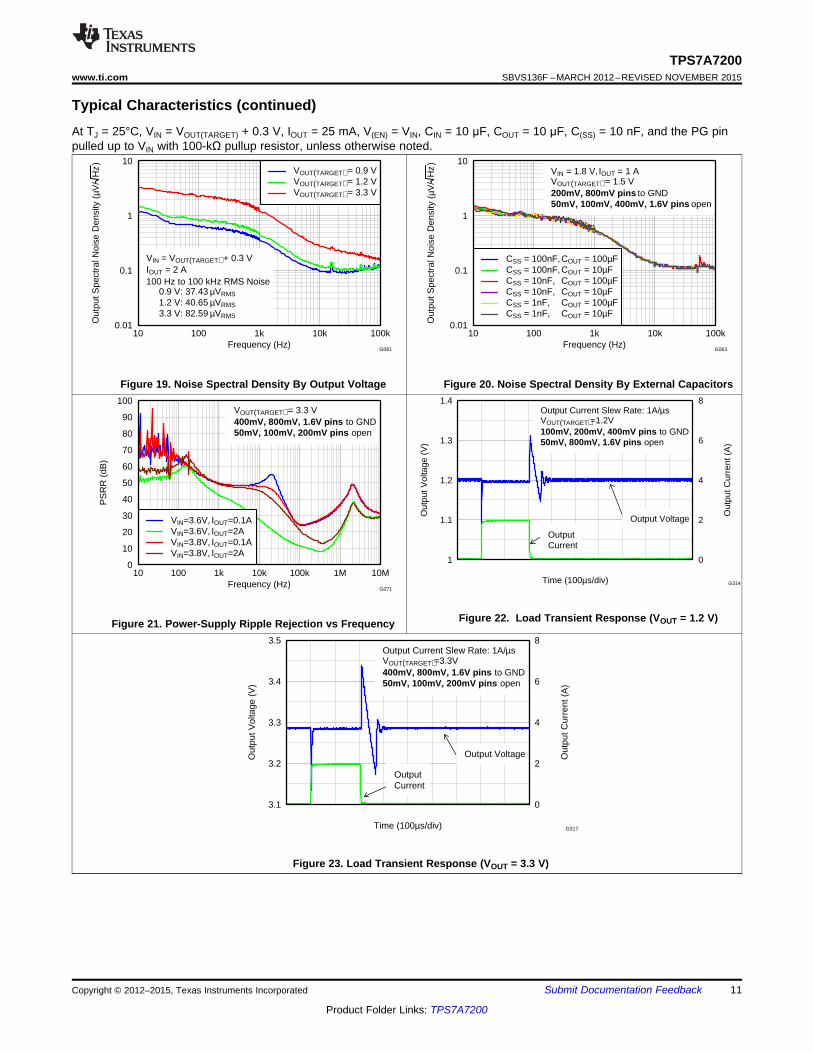
Typical Characteristics (continued)At TJ = 25°C, VIN = VOUT(TARGET) + 0.3 V, IOUT = 25 mA, V(EN) = VIN, CIN = 10 μF, COUT = 10 μF, C(SS) = 10 nF, and the PG pinpulled up to VIN with 100-kΩ pullup resistor, unless otherwise noted.
Figure 19. Noise Spectral Density By Output Voltage Figure 20. Noise Spectral Density By External Capacitors
Figure 21. Power-Supply Ripple Rejection vs Frequency Figure 22. Load Transient Response (VOUT = 1.2 V)
Figure 23. Load Transient Response (VOUT = 3.3 V)
Thermal
Protection
OUT
PG
IN
SS
EN Hysteresis
Current
Limit
UVLO
1.2-V Reference
0.45 V
GND
CSS
ChargePump
0.5-V Reference
70 kΩ50 kΩ
50 kΩ
3.2R
32R 16R 8R 4R 2R 1R
FB
SNS
1.6V800mV400mV200mV100mV50mV
700-µsDelay
Optional
12
TPS7A7200SBVS136F –MARCH 2012–REVISED NOVEMBER 2015 www.ti.com
Product Folder Links: TPS7A7200
Submit Documentation Feedback Copyright © 2012–2015, Texas Instruments Incorporated
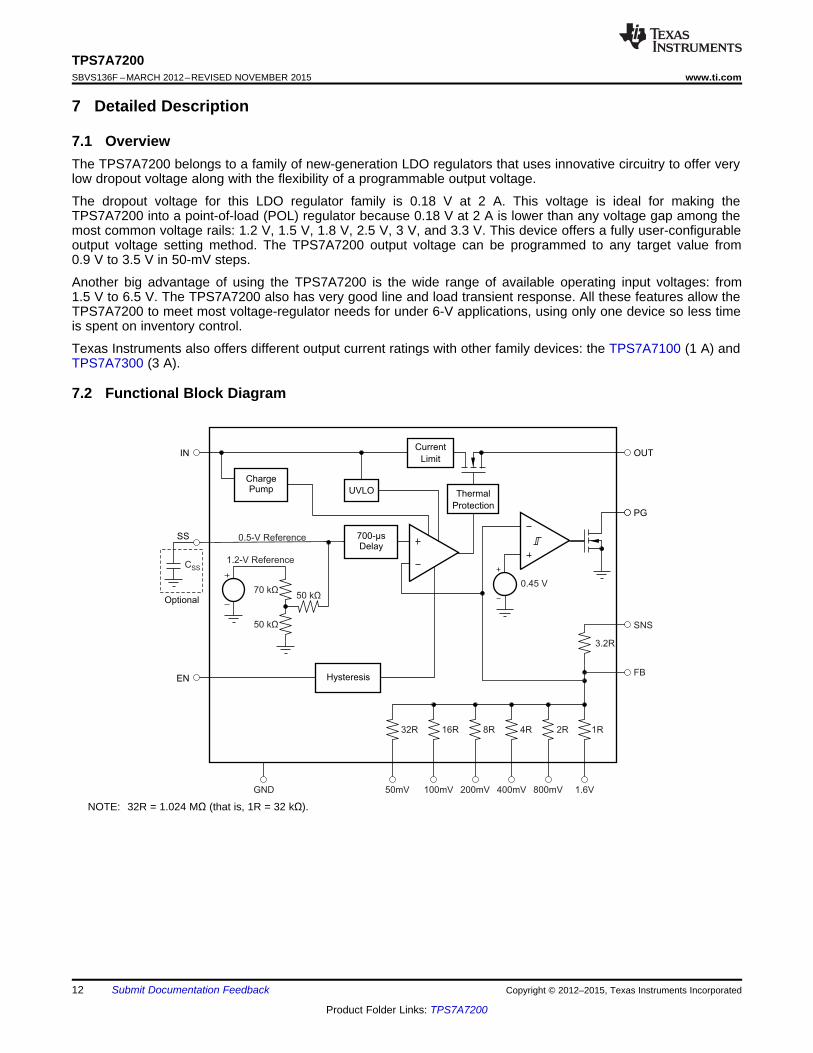
7 Detailed Description
7.1 OverviewThe TPS7A7200 belongs to a family of new-generation LDO regulators that uses innovative circuitry to offer verylow dropout voltage along with the flexibility of a programmable output voltage.
The dropout voltage for this LDO regulator family is 0.18 V at 2 A. This voltage is ideal for making theTPS7A7200 into a point-of-load (POL) regulator because 0.18 V at 2 A is lower than any voltage gap among themost common voltage rails: 1.2 V, 1.5 V, 1.8 V, 2.5 V, 3 V, and 3.3 V. This device offers a fully user-configurableoutput voltage setting method. The TPS7A7200 output voltage can be programmed to any target value from0.9 V to 3.5 V in 50-mV steps.
Another big advantage of using the TPS7A7200 is the wide range of available operating input voltages: from1.5 V to 6.5 V. The TPS7A7200 also has very good line and load transient response. All these features allow theTPS7A7200 to meet most voltage-regulator needs for under 6-V applications, using only one device so less timeis spent on inventory control.
Texas Instruments also offers different output current ratings with other family devices: the TPS7A7100 (1 A) andTPS7A7300 (3 A).
7.2 Functional Block Diagram
NOTE: 32R = 1.024 MΩ (that is, 1R = 32 kΩ).
V = 0.9 VOUT = 0.5 V + 400 mV
0.5 V is Vref
V = 0.5 V (1 + 3.2R/4R)´OUT
3.2R
32R 16R 8R 4R 2R 1R
VIN
OUT
SNS
FB
FB
0.5 V
50mV 100mV 200mV 400mV 800mV 1.6V
OUT
SNS
FB
PG
50mV
IN
Thermal Pad
EN
SS
NC
1.6V
10
0m
V
20
0m
V
GN
D
40
0m
V
80
0m
V
OU
T
OU
T
GN
D IN IN
Optional
CFF
CFF
13
TPS7A7200www.ti.com SBVS136F –MARCH 2012–REVISED NOVEMBER 2015
Product Folder Links: TPS7A7200
Submit Documentation FeedbackCopyright © 2012–2015, Texas Instruments Incorporated
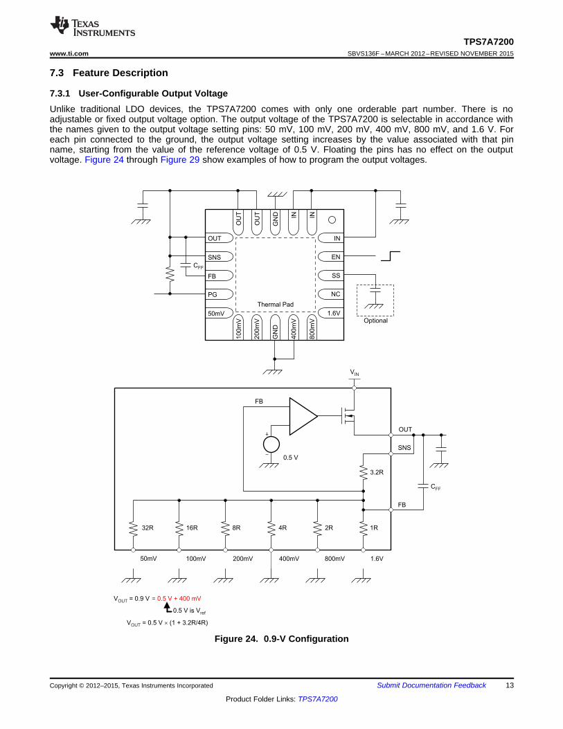
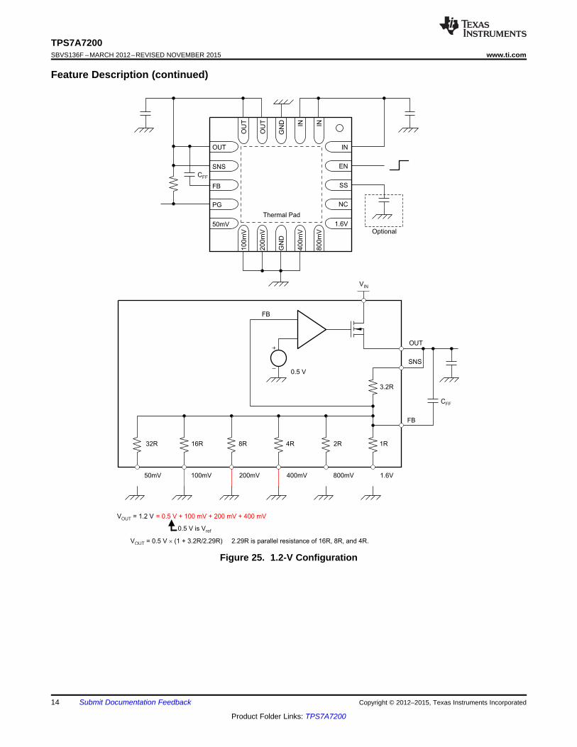
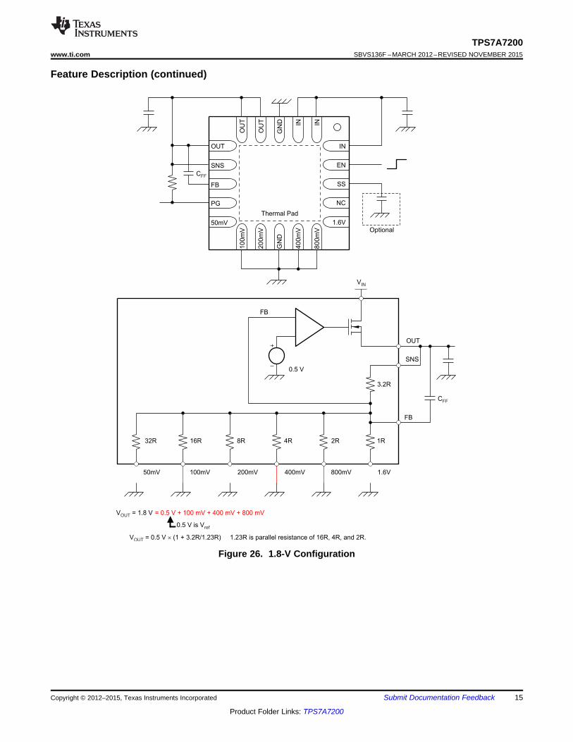
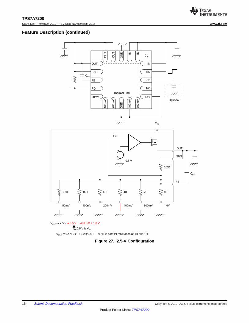
7.3 Feature Description
7.3.1 User-Configurable Output VoltageUnlike traditional LDO devices, the TPS7A7200 comes with only one orderable part number. There is noadjustable or fixed output voltage option. The output voltage of the TPS7A7200 is selectable in accordance withthe names given to the output voltage setting pins: 50 mV, 100 mV, 200 mV, 400 mV, 800 mV, and 1.6 V. Foreach pin connected to the ground, the output voltage setting increases by the value associated with that pinname, starting from the value of the reference voltage of 0.5 V. Floating the pins has no effect on the outputvoltage. Figure 24 through Figure 29 show examples of how to program the output voltages.
Figure 24. 0.9-V Configuration
V = 1.2 VOUT = 0.5 V + 100 mV + 200 mV + 400 mV
0.5 V is Vref
V = 0.5 V (1 + 3.2R/2.29R) 2.29R is parallel resistance of 16R, 8R, and 4R.´OUT
3.2R
32R 16R 8R 4R 2R 1R
VIN
OUT
SNS
FB
0.5 V
50mV 100mV 200mV 400mV 800mV 1.6V
OUT
SNS
FB
PG
50mV
IN
Thermal Pad
EN
SS
NC
1.6V
10
0m
V
20
0m
V
GN
D
40
0m
V
80
0m
V
OU
T
OU
T
GN
D IN IN
Optional
CFF
FB
CFF
14
TPS7A7200SBVS136F –MARCH 2012–REVISED NOVEMBER 2015 www.ti.com
Product Folder Links: TPS7A7200
Submit Documentation Feedback Copyright © 2012–2015, Texas Instruments Incorporated
Feature Description (continued)
Figure 25. 1.2-V Configuration
V = 1.8 VOUT = 0.5 V + 100 mV + 400 mV + 800 mV
0.5 V is Vref
V = 0.5 V (1 + 3.2R/1.23R) 1.23R is parallel resistance of 16R, 4R, and 2R.´OUT
3.2R
32R 16R 8R 4R 2R 1R
VIN
OUT
SNS
FB
0.5 V
50mV 100mV 200mV 400mV 800mV 1.6V
FB
CFF
OUT
SNS
FB
PG
50mV
IN
Thermal Pad
EN
SS
NC
1.6V
10
0m
V
20
0m
V
GN
D
40
0m
V
80
0m
V
OU
T
OU
T
GN
D IN IN
Optional
CFF
15
TPS7A7200www.ti.com SBVS136F –MARCH 2012–REVISED NOVEMBER 2015
Product Folder Links: TPS7A7200
Submit Documentation FeedbackCopyright © 2012–2015, Texas Instruments Incorporated
Feature Description (continued)
Figure 26. 1.8-V Configuration
V = 2.5 VOUT = 0.5 V + 400 mV + 1.6 V
0.5 V is Vref
V = 0.5 V (1 + 3.2R/0.8R) 0.8R is parallel resistance of 4R and 1R.´OUT
3.2R
32R 16R 8R 4R 2R 1R
VIN
OUT
SNS
FB
0.5 V
50mV 100mV 200mV 400mV 800mV 1.6V
OUT
SNS
FB
PG
50mV
IN
Thermal Pad
EN
SS
NC
1.6V
10
0m
V
20
0m
V
GN
D
40
0m
V
80
0m
V
OU
T
OU
T
GN
D IN IN
Optional
CFF
FB
CFF
16
TPS7A7200SBVS136F –MARCH 2012–REVISED NOVEMBER 2015 www.ti.com
Product Folder Links: TPS7A7200
Submit Documentation Feedback Copyright © 2012–2015, Texas Instruments Incorporated
Feature Description (continued)
Figure 27. 2.5-V Configuration
V = 3.3 VOUT = 0.5 V + 400 mV + 800 mV + 1.6 V
0.5 V is Vref
V = 0.5 V (1 + 3.2R/0.571R) 0.571R is parallel resistance of 4R, 2R, and 1R.´OUT
3.2R
32R 16R 8R 4R 2R 1R
VIN
OUT
SNS
FB
0.5 V
50mV 100mV 200mV 400mV 800mV 1.6V
OUT
SNS
FB
PG
50mV
IN
Thermal Pad
EN
SS
NC
1.6V
10
0m
V
20
0m
V
GN
D
40
0m
V
80
0m
V
OU
T
OU
T
GN
D IN IN
Optional
CFF
FB
CFF
17
TPS7A7200www.ti.com SBVS136F –MARCH 2012–REVISED NOVEMBER 2015
Product Folder Links: TPS7A7200
Submit Documentation FeedbackCopyright © 2012–2015, Texas Instruments Incorporated
Feature Description (continued)
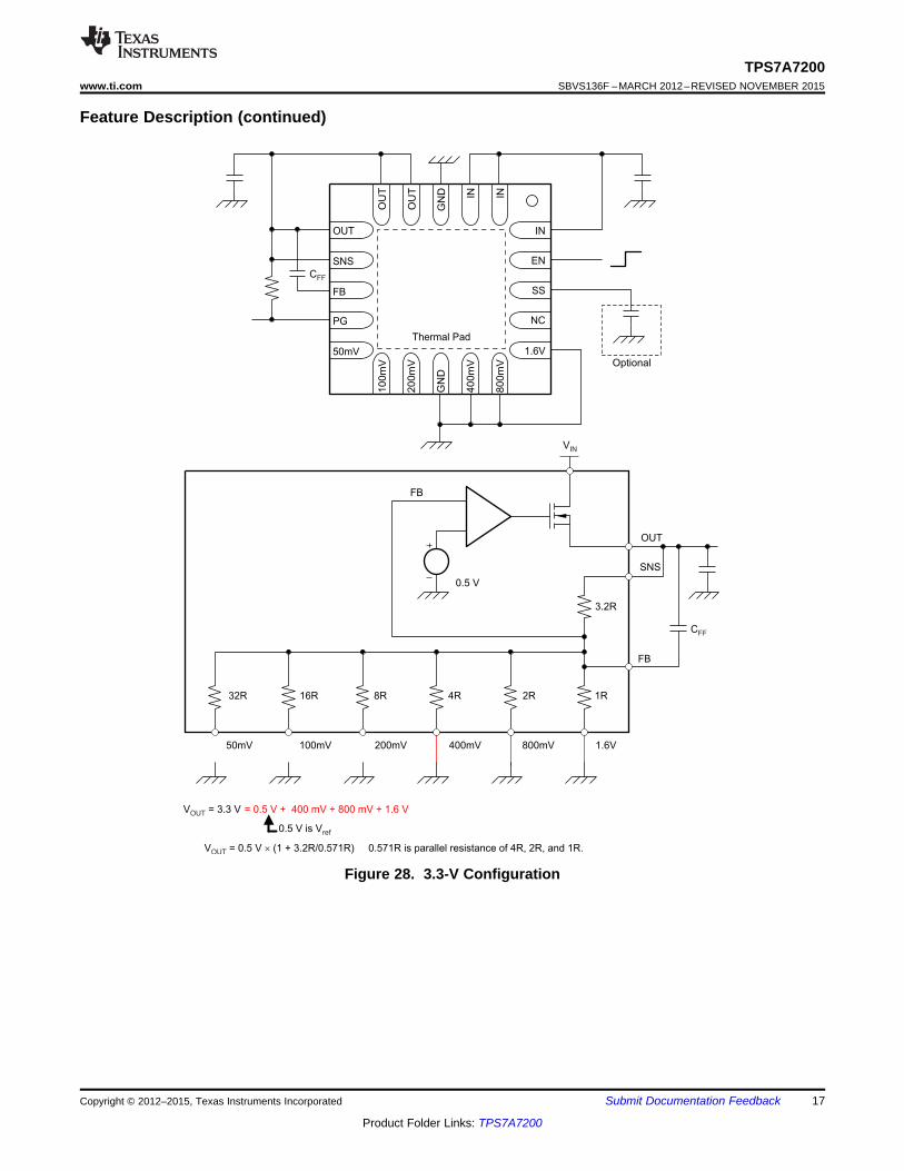
Figure 28. 3.3-V Configuration
V = 3.5 VOUT = 0.5 V + 200 mV + 400 mV + 800 mV + 1.6 V
0.5 V is Vref
V = 0.5 V (1 + 3.2R/0.533R) 0.533R is parallel resistance of 8R, 4R, 2R, and 1R.´OUT
3.2R
32R 16R 8R 4R 2R 1R
VIN
OUT
SNS
FB
0.5 V
50mV 100mV 200mV 400mV 800mV 1.6V
OUT
SNS
FB
PG
50mV
IN
Thermal Pad
EN
SS
NC
1.6V
10
0m
V
20
0m
V
GN
D
40
0m
V
80
0m
V
OU
T
OU
T
GN
D IN IN
Optional
FB
CFF
CFF
18
TPS7A7200SBVS136F –MARCH 2012–REVISED NOVEMBER 2015 www.ti.com
Product Folder Links: TPS7A7200
Submit Documentation Feedback Copyright © 2012–2015, Texas Instruments Incorporated
Feature Description (continued)
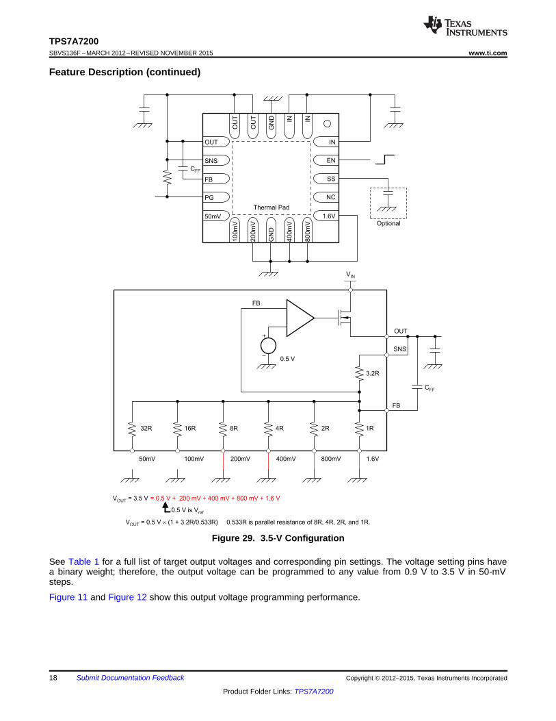
Figure 29. 3.5-V Configuration
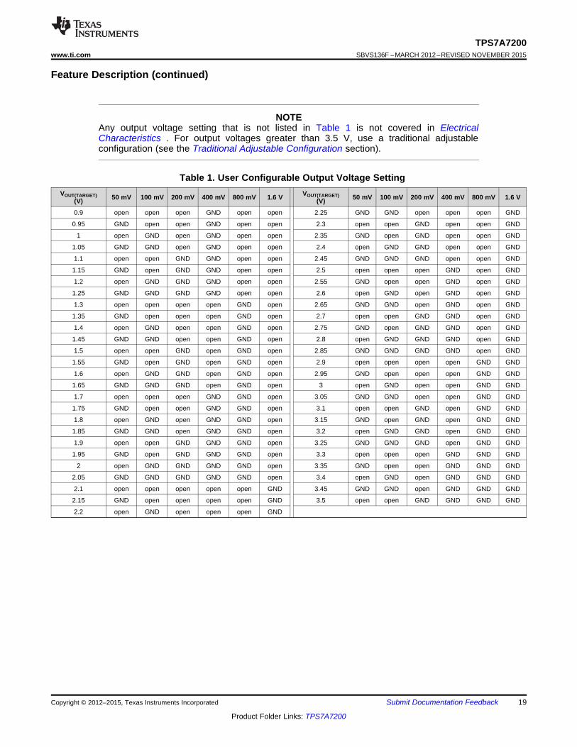
See Table 1 for a full list of target output voltages and corresponding pin settings. The voltage setting pins havea binary weight; therefore, the output voltage can be programmed to any value from 0.9 V to 3.5 V in 50-mVsteps.
Figure 11 and Figure 12 show this output voltage programming performance.
19
TPS7A7200www.ti.com SBVS136F –MARCH 2012–REVISED NOVEMBER 2015
Product Folder Links: TPS7A7200
Submit Documentation FeedbackCopyright © 2012–2015, Texas Instruments Incorporated
Feature Description (continued)SPACE
NOTEAny output voltage setting that is not listed in Table 1 is not covered in ElectricalCharacteristics . For output voltages greater than 3.5 V, use a traditional adjustableconfiguration (see the Traditional Adjustable Configuration section).
Table 1. User Configurable Output Voltage SettingVOUT(TARGET)
(V) 50 mV 100 mV 200 mV 400 mV 800 mV 1.6 V VOUT(TARGET)(V) 50 mV 100 mV 200 mV 400 mV 800 mV 1.6 V
0.9 open open open GND open open 2.25 GND GND open open open GND
0.95 GND open open GND open open 2.3 open open GND open open GND
1 open GND open GND open open 2.35 GND open GND open open GND
1.05 GND GND open GND open open 2.4 open GND GND open open GND
1.1 open open GND GND open open 2.45 GND GND GND open open GND
1.15 GND open GND GND open open 2.5 open open open GND open GND
1.2 open GND GND GND open open 2.55 GND open open GND open GND
1.25 GND GND GND GND open open 2.6 open GND open GND open GND
1.3 open open open open GND open 2.65 GND GND open GND open GND
1.35 GND open open open GND open 2.7 open open GND GND open GND
1.4 open GND open open GND open 2.75 GND open GND GND open GND
1.45 GND GND open open GND open 2.8 open GND GND GND open GND
1.5 open open GND open GND open 2.85 GND GND GND GND open GND
1.55 GND open GND open GND open 2.9 open open open open GND GND
1.6 open GND GND open GND open 2.95 GND open open open GND GND
1.65 GND GND GND open GND open 3 open GND open open GND GND
1.7 open open open GND GND open 3.05 GND GND open open GND GND
1.75 GND open open GND GND open 3.1 open open GND open GND GND
1.8 open GND open GND GND open 3.15 GND open GND open GND GND
1.85 GND GND open GND GND open 3.2 open GND GND open GND GND
1.9 open open GND GND GND open 3.25 GND GND GND open GND GND
1.95 GND open GND GND GND open 3.3 open open open GND GND GND
2 open GND GND GND GND open 3.35 GND open open GND GND GND
2.05 GND GND GND GND GND open 3.4 open GND open GND GND GND
2.1 open open open open open GND 3.45 GND GND open GND GND GND
2.15 GND open open open open GND 3.5 open open GND GND GND GND
2.2 open GND open open open GND
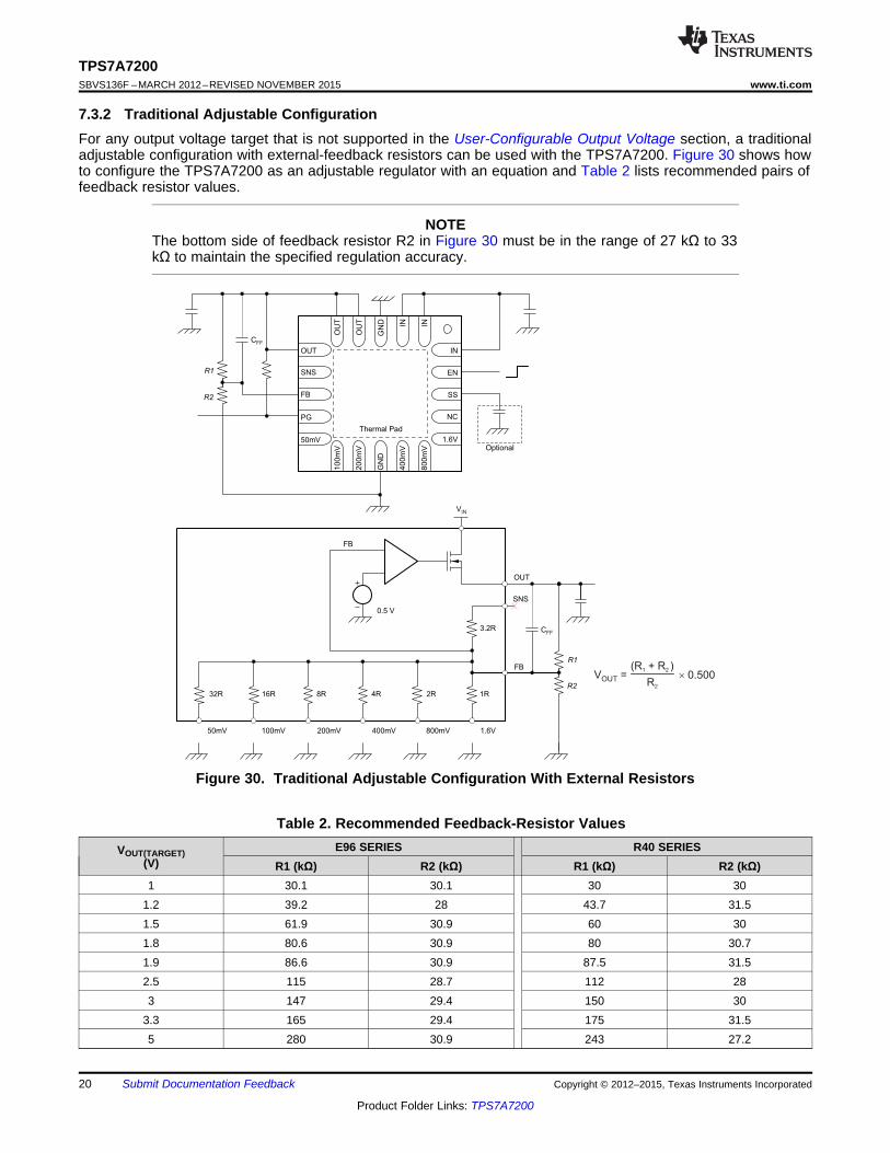
3.2R
32R 16R 8R 4R 2R 1R
VIN
OUT
SNS
FB
FB
0.5 V
50mV 100mV 200mV 400mV 800mV 1.6V
OUT
SNS
FB
PG
50mV
IN
Thermal Pad
EN
SS
NC
1.6V
10
0m
V
20
0m
V
GN
D
40
0m
V
80
0m
V
OU
T
OU
T
GN
D IN IN
R1
R2
R1
R2
Optional
V =OUT ´ 0.500(R + R )1 2
R2
CFF
CFF
20
TPS7A7200SBVS136F –MARCH 2012–REVISED NOVEMBER 2015 www.ti.com
Product Folder Links: TPS7A7200
Submit Documentation Feedback Copyright © 2012–2015, Texas Instruments Incorporated
7.3.2 Traditional Adjustable ConfigurationFor any output voltage target that is not supported in the User-Configurable Output Voltage section, a traditionaladjustable configuration with external-feedback resistors can be used with the TPS7A7200. Figure 30 shows howto configure the TPS7A7200 as an adjustable regulator with an equation and Table 2 lists recommended pairs offeedback resistor values.
NOTEThe bottom side of feedback resistor R2 in Figure 30 must be in the range of 27 kΩ to 33kΩ to maintain the specified regulation accuracy.
Figure 30. Traditional Adjustable Configuration With External Resistors
Table 2. Recommended Feedback-Resistor Values
VOUT(TARGET)(V)
E96 SERIES R40 SERIESR1 (kΩ) R2 (kΩ) R1 (kΩ) R2 (kΩ)
1 30.1 30.1 30 301.2 39.2 28 43.7 31.51.5 61.9 30.9 60 301.8 80.6 30.9 80 30.71.9 86.6 30.9 87.5 31.52.5 115 28.7 112 283 147 29.4 150 30
3.3 165 29.4 175 31.55 280 30.9 243 27.2
21
TPS7A7200www.ti.com SBVS136F –MARCH 2012–REVISED NOVEMBER 2015
Product Folder Links: TPS7A7200
Submit Documentation FeedbackCopyright © 2012–2015, Texas Instruments Incorporated
7.3.3 Undervoltage Lockout (UVLO)The TPS7A7200 uses an undervoltage lockout circuit to keep the output shut off until the internal circuitry isoperating properly. The UVLO circuit has a deglitch feature that typically ignores undershoot of the input voltageupon the event of device start-up. Still, a poor input line impedance may cause a severe input voltage drop whenthe device powers on. As explained in the Input Capacitor Requirements section, the input line impedance mustbe well-designed.
7.3.4 Soft-StartThe TPS7A7200 has an SS pin that provides a soft-start (slow start) function.
By leaving the SS pin open, the TPS7A7200 performs a soft-start by its default setting.
As shown in Functional Block Diagram, by connecting a capacitor between the SS pin and the ground, the CSScapacitor forms an RC pair together with the integrated 50-kΩ resistor. The RC pair operates as an RC-delaycircuit for the soft-start together with the internal 700-µs delay circuit.
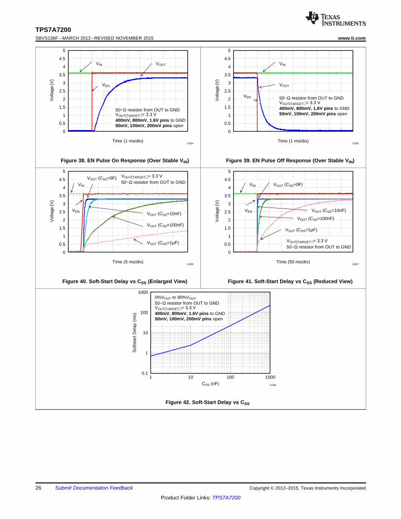
The relationship between CSS and the soft-start time is shown in Figure 40 through Figure 42.
7.3.5 Current LimitThe TPS7A7200 internal current limit circuitry protects the regulator during fault conditions. During a current limitevent, the output sources a fixed amount of current that is mostly independent of the output voltage. The currentlimit function is provided as a fail-safe mechanism and is not intended to be used regularly. Do not design anyapplications to use this current limit function as a part of expected normal operation. Extended periods of currentlimit operation degrade device reliability.
Powering on the device with the enable pin, or increasing the input voltage above the minimum operating voltagewhile a low-impedance short exists on the output of the device, may result in a sequence of high-current pulsesfrom the input to the output of the device. The energy consumed by the device is minimal during these events;therefore, there is no failure risk. Additional input capacitance helps to mitigate the load transient requirement ofthe upstream supply during these events.
7.3.6 EnableThe EN pin switches the enable and disable (shutdown) states of the TPS7A7200. A logic high input at the ENpin enables the device; a logic low input disables the device. When disabled, the device current consumption isreduced.
7.3.7 Power GoodThe TPS7A7200 has a power good function that works with the PG output pin. When the output voltageundershoots the threshold voltage VIT(PG) during normal operation, the PG open-drain output turns from a high-impedance state to a low-impedance state. When the output voltage exceeds the VIT(PG) threshold by an amountgreater than the PG hysteresis, Vhys(PG), the PG open-drain output turns from a low-impedance state to high-impedance state. By connecting a pullup resistor (usually between OUT and PG pins), any downstream devicecan receive an active-high enable logic signal.
When setting the output voltage to less than 1.8 V and using a pullup resistor between OUT and PG pins,depending on the downstream device specifications, the downstream device may not accept the PG output as avalid high-level logic voltage. In such cases, place a pullup resistor between IN and PG pins, not between OUTand PG pins.
Figure 18 shows the open-drain output drive capability. The on-resistance of the open-drain transistor iscalculated using Figure 18, and is approximately 200 Ω. Any pullup resistor greater than 10 kΩ works fine for thispurpose.
22
TPS7A7200SBVS136F –MARCH 2012–REVISED NOVEMBER 2015 www.ti.com
Product Folder Links: TPS7A7200
Submit Documentation Feedback Copyright © 2012–2015, Texas Instruments Incorporated
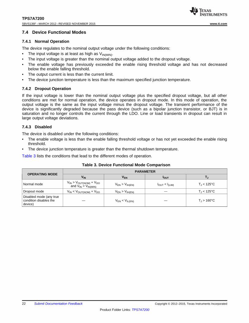
7.4 Device Functional Modes
7.4.1 Normal OperationThe device regulates to the nominal output voltage under the following conditions:• The input voltage is at least as high as VIN(MIN).• The input voltage is greater than the nominal output voltage added to the dropout voltage.• The enable voltage has previously exceeded the enable rising threshold voltage and has not decreased
below the enable falling threshold.• The output current is less than the current limit.• The device junction temperature is less than the maximum specified junction temperature.
7.4.2 Dropout OperationIf the input voltage is lower than the nominal output voltage plus the specified dropout voltage, but all otherconditions are met for normal operation, the device operates in dropout mode. In this mode of operation, theoutput voltage is the same as the input voltage minus the dropout voltage. The transient performance of thedevice is significantly degraded because the pass device (such as a bipolar junction transistor, or BJT) is insaturation and no longer controls the current through the LDO. Line or load transients in dropout can result inlarge output voltage deviations.
7.4.3 DisabledThe device is disabled under the following conditions:• The enable voltage is less than the enable falling threshold voltage or has not yet exceeded the enable rising
threshold.• The device junction temperature is greater than the thermal shutdown temperature.
Table 3 lists the conditions that lead to the different modes of operation.
Table 3. Device Functional Mode Comparison
OPERATING MODEPARAMETER
VIN VEN IOUT TJ
Normal mode VIN > VOUT(NOM) + VDOand VIN > VIN(MIN)
VEN > VIH(EN) IOUT < I(LIM) TJ < 125°C
Dropout mode VIN < VOUT(NOM) + VDO VEN > VIH(EN) — TJ < 125°CDisabled mode (any truecondition disables thedevice)
— VEN < VIL(EN) — TJ > 160°C
IN
EN
SS
PG
OUT
SNSCSS
CIN
COUT
1.5 V
GND
1.2 V = 0.5 V
+ 100 mV+ 200 mV+ 400 mV
ref
TPS7A7200
FB
1.6V
800mV400mV200mV
100mV
50mV
Optional
CFF
23
TPS7A7200www.ti.com SBVS136F –MARCH 2012–REVISED NOVEMBER 2015
Product Folder Links: TPS7A7200
Submit Documentation FeedbackCopyright © 2012–2015, Texas Instruments Incorporated
8 Application and Implementation
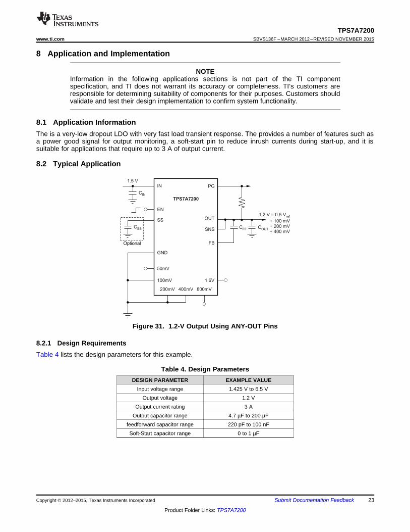
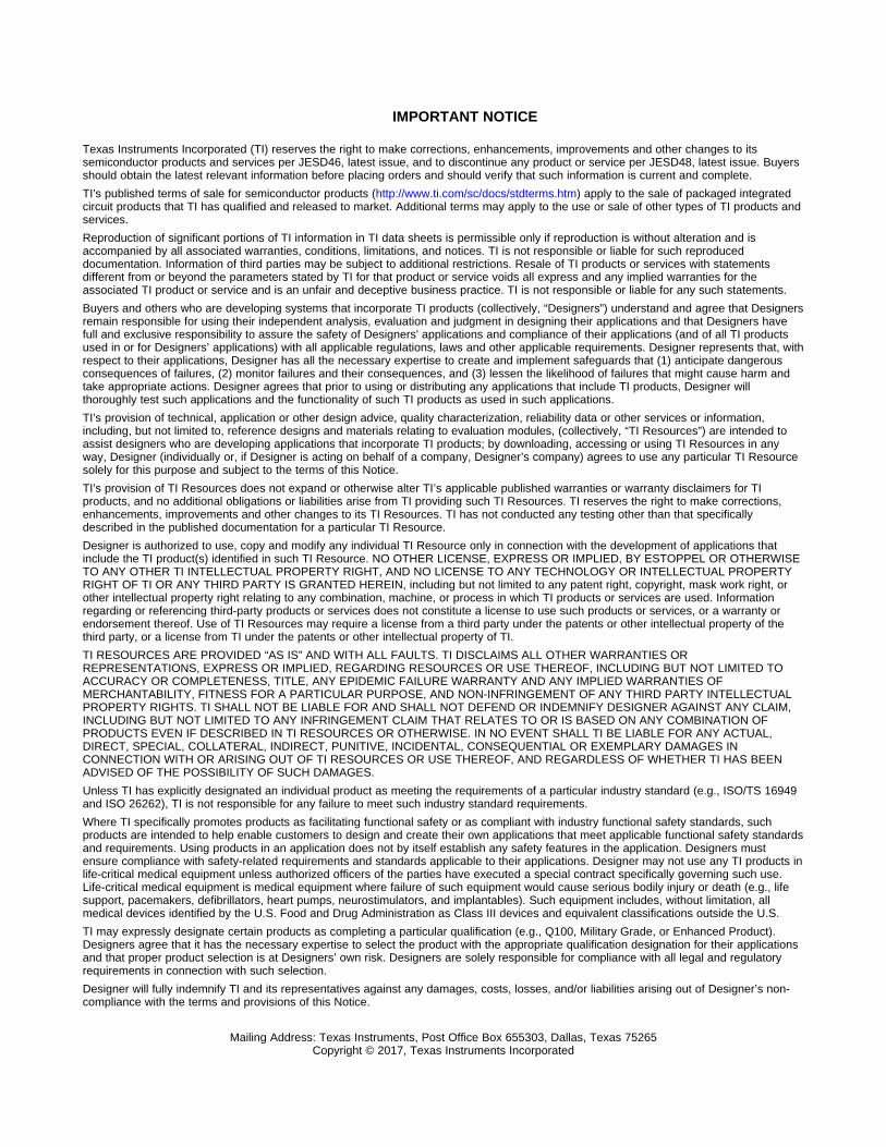
NOTEInformation in the following applications sections is not part of the TI componentspecification, and TI does not warrant its accuracy or completeness. TI’s customers areresponsible for determining suitability of components for their purposes. Customers shouldvalidate and test their design implementation to confirm system functionality.
8.1 Application InformationThe is a very-low dropout LDO with very fast load transient response. The provides a number of features such asa power good signal for output monitoring, a soft-start pin to reduce inrush currents during start-up, and it issuitable for applications that require up to 3 A of output current.
8.2 Typical Application
Figure 31. 1.2-V Output Using ANY-OUT Pins
8.2.1 Design RequirementsTable 4 lists the design parameters for this example.
Table 4. Design ParametersDESIGN PARAMETER EXAMPLE VALUE
Input voltage range 1.425 V to 6.5 VOutput voltage 1.2 V
Output current rating 3 AOutput capacitor range 4.7 µF to 200 µF
feedforward capacitor range 220 pF to 100 nFSoft-Start capacitor range 0 to 1 µF
24
TPS7A7200SBVS136F –MARCH 2012–REVISED NOVEMBER 2015 www.ti.com
Product Folder Links: TPS7A7200
Submit Documentation Feedback Copyright © 2012–2015, Texas Instruments Incorporated
8.2.2 Detailed Design Procedure
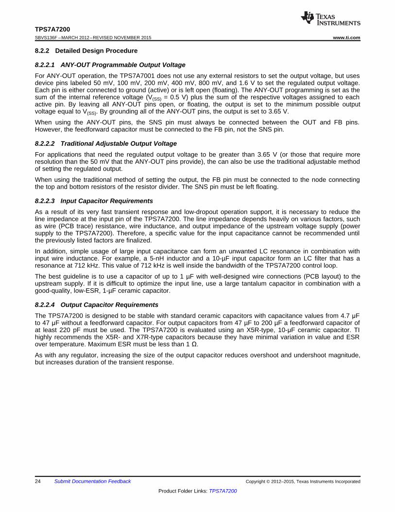
8.2.2.1 ANY-OUT Programmable Output VoltageFor ANY-OUT operation, the TPS7A7001 does not use any external resistors to set the output voltage, but usesdevice pins labeled 50 mV, 100 mV, 200 mV, 400 mV, 800 mV, and 1.6 V to set the regulated output voltage.Each pin is either connected to ground (active) or is left open (floating). The ANY-OUT programming is set as thesum of the internal reference voltage (V(SS) = 0.5 V) plus the sum of the respective voltages assigned to eachactive pin. By leaving all ANY-OUT pins open, or floating, the output is set to the minimum possible outputvoltage equal to V(SS). By grounding all of the ANY-OUT pins, the output is set to 3.65 V.
When using the ANY-OUT pins, the SNS pin must always be connected between the OUT and FB pins.However, the feedforward capacitor must be connected to the FB pin, not the SNS pin.
8.2.2.2 Traditional Adjustable Output VoltageFor applications that need the regulated output voltage to be greater than 3.65 V (or those that require moreresolution than the 50 mV that the ANY-OUT pins provide), the can also be use the traditional adjustable methodof setting the regulated output.
When using the traditional method of setting the output, the FB pin must be connected to the node connectingthe top and bottom resistors of the resistor divider. The SNS pin must be left floating.
8.2.2.3 Input Capacitor RequirementsAs a result of its very fast transient response and low-dropout operation support, it is necessary to reduce theline impedance at the input pin of the TPS7A7200. The line impedance depends heavily on various factors, suchas wire (PCB trace) resistance, wire inductance, and output impedance of the upstream voltage supply (powersupply to the TPS7A7200). Therefore, a specific value for the input capacitance cannot be recommended untilthe previously listed factors are finalized.
In addition, simple usage of large input capacitance can form an unwanted LC resonance in combination withinput wire inductance. For example, a 5-nH inductor and a 10-µF input capacitor form an LC filter that has aresonance at 712 kHz. This value of 712 kHz is well inside the bandwidth of the TPS7A7200 control loop.
The best guideline is to use a capacitor of up to 1 µF with well-designed wire connections (PCB layout) to theupstream supply. If it is difficult to optimize the input line, use a large tantalum capacitor in combination with agood-quality, low-ESR, 1-µF ceramic capacitor.
8.2.2.4 Output Capacitor RequirementsThe TPS7A7200 is designed to be stable with standard ceramic capacitors with capacitance values from 4.7 μFto 47 μF without a feedforward capacitor. For output capacitors from 47 µF to 200 µF a feedforward capacitor ofat least 220 pF must be used. The TPS7A7200 is evaluated using an X5R-type, 10-μF ceramic capacitor. TIhighly recommends the X5R- and X7R-type capacitors because they have minimal variation in value and ESRover temperature. Maximum ESR must be less than 1 Ω.
As with any regulator, increasing the size of the output capacitor reduces overshoot and undershoot magnitude,but increases duration of the transient response.
0
0.5
1
1.5
2
2.5
3
3.5
4
4.5
5
VIN
VOUT
Time (1 ms/div)
Vol
tage
(V
)
IN = EN50−Ω resistor from OUT to GNDVOUT(TARGET) = 3.3 V400mV, 800mV, 1.6V pins to GND50mV, 100mV, 200mV pins open
G302
0
0.5
1
1.5
2
2.5
3
3.5
4
4.5
5
VIN
VOUT
Time (1 ms/div)
Vol
tage
(V
)
IN = EN50−Ω resistor from OUT to GNDVOUT(TARGET) = 3.3 V400mV, 800mV, 1.6V pins to GND50mV, 100mV, 200mV pins open
G303
3.2
3.4
3.6
3.8
4
4.2
4.4
4.6
VIN
VOUT
Time (20 µs/div)
Vol
tage
(V
)
IOUT=1A, VOUT(TARGET)=3.3V400mV, 800mV, 1.6V pins to GND50mV, 100mV, 200mV pins open
G300
00.5
11.5
22.5
33.5
44.5
55.5
66.5
7
VIN
VOUT
Time (2 ms/div)
Vol
tage
(V
)
VOUT(TARGET)=3.3V400mV, 800mV,1.6V pins to GND50mV, 100mV,200mV pins open
50−Ω resistor between OUT and GND
G301
1
1.1
1.2
1.3
1.4
Output Voltage
0
1
2
3
4
Time (100µs/div)
Out
put V
olta
ge (
V)
Out
put C
urre
nt (
A)
OutputCurrent
Output Current Slew Rate: 1A/µsVOUT(TARGET)=1.2V100mV, 200mV, 400mV pins to GND50mV, 800mV, 1.6V pins open
G313
3.1
3.2
3.3
3.4
3.5
Output Voltage
0
1
2
3
4
Time (100µs/div)
Out
put V
olta
ge (
V)
Out
put C
urre
nt (
A)
OutputCurrent
Output Current Slew Rate: 1A/µsVOUT(TARGET)=3.3V400mV, 800mV, 1.6V pins to GND50mV, 100mV, 200mV pins open
G316
25
TPS7A7200www.ti.com SBVS136F –MARCH 2012–REVISED NOVEMBER 2015
Product Folder Links: TPS7A7200
Submit Documentation FeedbackCopyright © 2012–2015, Texas Instruments Incorporated
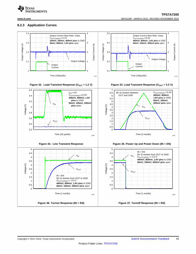
8.2.3 Application Curves
Figure 32. Load Transient Response (VOUT = 1.2 V) Figure 33. Load Transient Response (VOUT = 3.3 V)
Figure 34. Line Transient Response Figure 35. Power Up and Power Down (IN = EN)
Figure 36. Turnon Response (IN = EN) Figure 37. Turnoff Response (IN = EN)
0.1
1
10
100
1000
1 10 100 1000CSS (nF)
Sof
tsta
rt D
elay
(m
s)
0%VOUT to 90%VOUT
50−Ω resistor from OUT to GNDVOUT(TARGET) = 3.3 V400mV, 800mV, 1.6V pins to GND50mV, 100mV, 200mV pins open
G308
0
0.5
1
1.5
2
2.5
3
3.5
4
4.5
5
VIN
VOUT (CSS=0F)
VEN VOUT (CSS=10nF)
VOUT (CSS=100nF)
VOUT (CSS=1µF)
Time (5 ms/div)
Vol
tage
(V
)
VOUT(TARGET) = 3.3 V50−Ω resistor from OUT to GND
G306
0
0.5
1
1.5
2
2.5
3
3.5
4
4.5
5
VIN VOUT (CSS=0F)
VEN VOUT (CSS=10nF)
VOUT (CSS=100nF)
VOUT (CSS=1µF)
Time (50 ms/div)
Vol
tage
(V
)
VOUT(TARGET) = 3.3 V50−Ω resistor from OUT to GND
G307
0
0.5
1
1.5
2
2.5
3
3.5
4
4.5
5
VIN VOUT
VEN
Time (1 ms/div)
Vol
tage
(V
)
50−Ω resistor from OUT to GNDVOUT(TARGET) = 3.3 V400mV, 800mV, 1.6V pins to GND50mV, 100mV, 200mV pins open
G304
0
0.5
1
1.5
2
2.5
3
3.5
4
4.5
5
VIN
VOUT
VEN
Time (1 ms/div)
Vol
tage
(V
)
50−Ω resistor from OUT to GNDVOUT(TARGET) = 3.3 V400mV, 800mV, 1.6V pins to GND50mV, 100mV, 200mV pins open
G305
26
TPS7A7200SBVS136F –MARCH 2012–REVISED NOVEMBER 2015 www.ti.com
Product Folder Links: TPS7A7200
Submit Documentation Feedback Copyright © 2012–2015, Texas Instruments Incorporated
Figure 38. EN Pulse On Response (Over Stable VIN) Figure 39. EN Pulse Off Response (Over Stable VIN)
Figure 40. Soft-Start Delay vs CSS (Enlarged View) Figure 41. Soft-Start Delay vs CSS (Reduced View)
Figure 42. Soft-Start Delay vs CSS
SNS
OUT
50 mV
100
mV
IN
1.6 V
CIN
COUT
Input Output
EN
SS
GN
D
FB
PG
200
mV
400
mV
800
mV
NC
IN OU
T
IN OU
T
GN
D
CSSR2
R1
Ground
ThermalPad
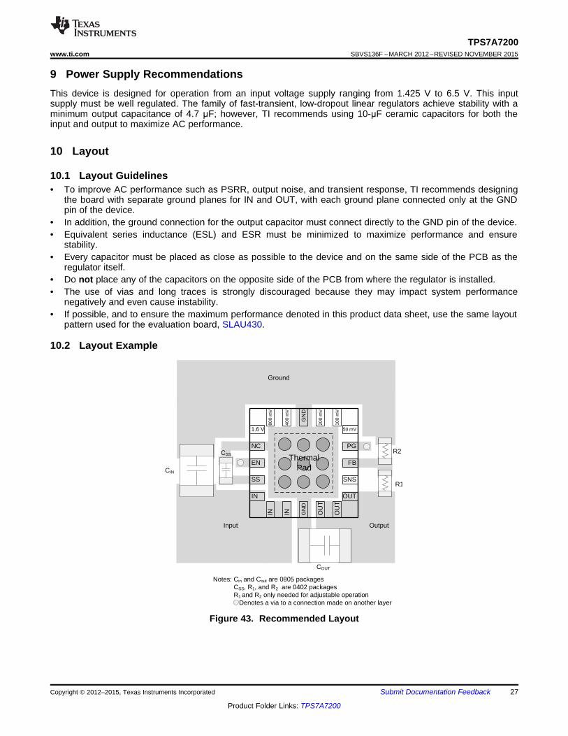
Notes: Cin and Cout are 0805 packages CSS, R1, and R2 are 0402 packages
R1 and R2 only needed for adjustable operation Denotes a via to a connection made on another layer
27
TPS7A7200www.ti.com SBVS136F –MARCH 2012–REVISED NOVEMBER 2015
Product Folder Links: TPS7A7200
Submit Documentation FeedbackCopyright © 2012–2015, Texas Instruments Incorporated
9 Power Supply RecommendationsThis device is designed for operation from an input voltage supply ranging from 1.425 V to 6.5 V. This inputsupply must be well regulated. The family of fast-transient, low-dropout linear regulators achieve stability with aminimum output capacitance of 4.7 μF; however, TI recommends using 10-μF ceramic capacitors for both theinput and output to maximize AC performance.
10 Layout
10.1 Layout Guidelines• To improve AC performance such as PSRR, output noise, and transient response, TI recommends designing
the board with separate ground planes for IN and OUT, with each ground plane connected only at the GNDpin of the device.
• In addition, the ground connection for the output capacitor must connect directly to the GND pin of the device.• Equivalent series inductance (ESL) and ESR must be minimized to maximize performance and ensure
stability.• Every capacitor must be placed as close as possible to the device and on the same side of the PCB as the
regulator itself.• Do not place any of the capacitors on the opposite side of the PCB from where the regulator is installed.• The use of vias and long traces is strongly discouraged because they may impact system performance
negatively and even cause instability.• If possible, and to ensure the maximum performance denoted in this product data sheet, use the same layout
pattern used for the evaluation board, SLAU430.
10.2 Layout Example
Figure 43. Recommended Layout
0
20
40
60
80
100
120
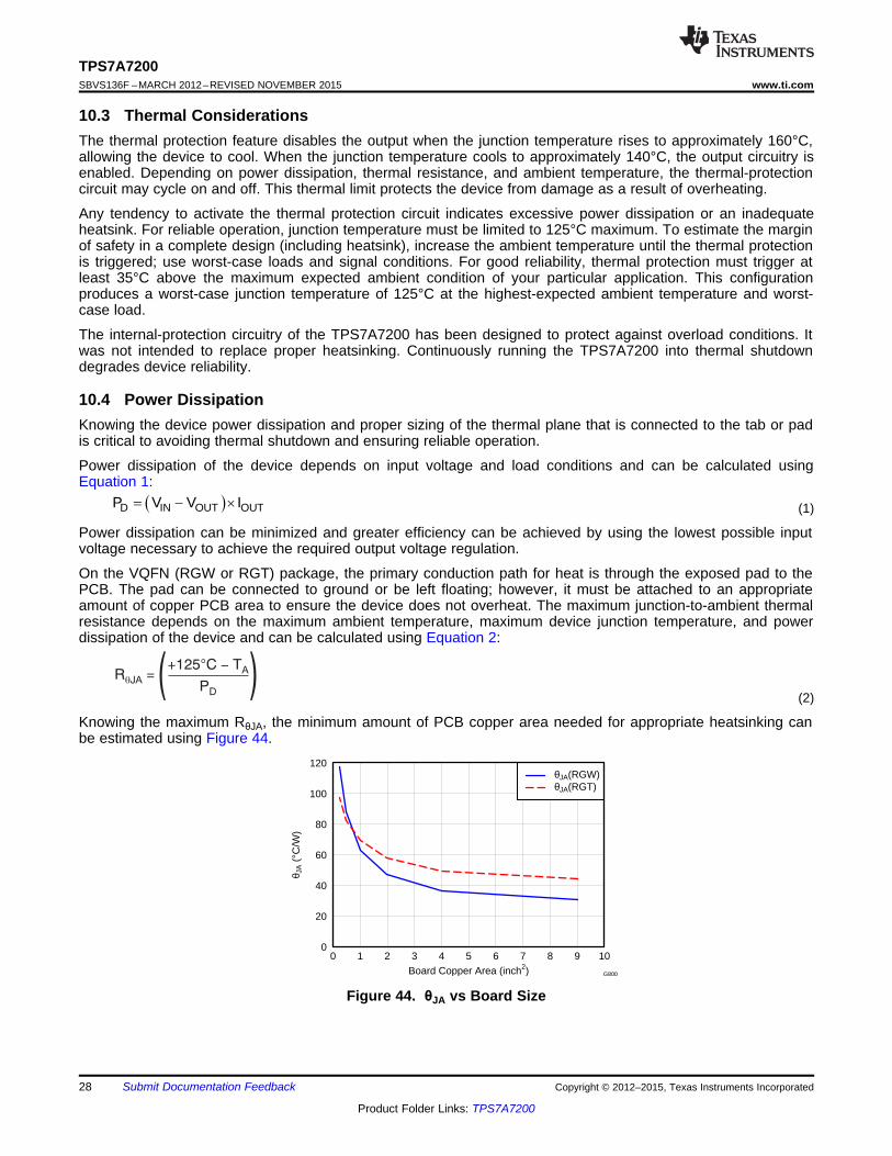
0 1 2 3 4 5 6 7 8 9 10Board Copper Area (inch2)
θ JA (
°C/W
)
θJA(RGW)θJA(RGT)
G800
R =qJA
+125 C T° -A
PD
D IN OUT OUTP V V I u
28
TPS7A7200SBVS136F –MARCH 2012–REVISED NOVEMBER 2015 www.ti.com
Product Folder Links: TPS7A7200
Submit Documentation Feedback Copyright © 2012–2015, Texas Instruments Incorporated
10.3 Thermal ConsiderationsThe thermal protection feature disables the output when the junction temperature rises to approximately 160°C,allowing the device to cool. When the junction temperature cools to approximately 140°C, the output circuitry isenabled. Depending on power dissipation, thermal resistance, and ambient temperature, the thermal-protectioncircuit may cycle on and off. This thermal limit protects the device from damage as a result of overheating.
Any tendency to activate the thermal protection circuit indicates excessive power dissipation or an inadequateheatsink. For reliable operation, junction temperature must be limited to 125°C maximum. To estimate the marginof safety in a complete design (including heatsink), increase the ambient temperature until the thermal protectionis triggered; use worst-case loads and signal conditions. For good reliability, thermal protection must trigger atleast 35°C above the maximum expected ambient condition of your particular application. This configurationproduces a worst-case junction temperature of 125°C at the highest-expected ambient temperature and worst-case load.
The internal-protection circuitry of the TPS7A7200 has been designed to protect against overload conditions. Itwas not intended to replace proper heatsinking. Continuously running the TPS7A7200 into thermal shutdowndegrades device reliability.
10.4 Power DissipationKnowing the device power dissipation and proper sizing of the thermal plane that is connected to the tab or padis critical to avoiding thermal shutdown and ensuring reliable operation.
Power dissipation of the device depends on input voltage and load conditions and can be calculated usingEquation 1:
(1)
Power dissipation can be minimized and greater efficiency can be achieved by using the lowest possible inputvoltage necessary to achieve the required output voltage regulation.
On the VQFN (RGW or RGT) package, the primary conduction path for heat is through the exposed pad to thePCB. The pad can be connected to ground or be left floating; however, it must be attached to an appropriateamount of copper PCB area to ensure the device does not overheat. The maximum junction-to-ambient thermalresistance depends on the maximum ambient temperature, maximum device junction temperature, and powerdissipation of the device and can be calculated using Equation 2:
(2)
Knowing the maximum RθJA, the minimum amount of PCB copper area needed for appropriate heatsinking canbe estimated using Figure 44.
Figure 44. θJA vs Board Size
T on PCBB
T on of ICtopT
1mm
(a) Example RGW (QFN) Package Measurement
Y YJT J T JT D
: T = T + P·
Y YJB J B JB D
: T = T + P·
29
TPS7A7200www.ti.com SBVS136F –MARCH 2012–REVISED NOVEMBER 2015
Product Folder Links: TPS7A7200
Submit Documentation FeedbackCopyright © 2012–2015, Texas Instruments Incorporated
Power Dissipation (continued)shows the variation of θJA as a function of ground plane copper area in the board. It is intended only as aguideline to demonstrate the effects of heat spreading in the ground plane and must not be used to estimateactual thermal performance in real application environments.
NOTEWhen the device is mounted on an application PCB, TI strongly recommends using ΨJTand ΨJB, as explained in the Estimating Junction Temperature section.
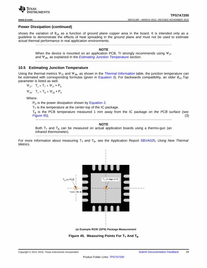
10.5 Estimating Junction TemperatureUsing the thermal metrics ΨJT and ΨJB, as shown in the Thermal Information table, the junction temperature canbe estimated with corresponding formulas (given in Equation 3). For backwards compatibility, an older θJC,Topparameter is listed as well.
Where:PD is the power dissipation shown by Equation 2.TT is the temperature at the center-top of the IC package.TB is the PCB temperature measured 1 mm away from the IC package on the PCB surface (seeFigure 45). (3)
NOTEBoth TT and TB can be measured on actual application boards using a thermo-gun (aninfrared thermometer).
For more information about measuring TT and TB, see the Application Report SBVA025, Using New ThermalMetrics.
Figure 45. Measuring Points For TT And TB
0
5
10
15
20
25
0 1 2 3 4 5 6 7 8 9 10
ψJB(RGW)
ψJB(RGT)
ψJT(RGW)ψJT(RGT)
Board Copper Area (inch2)
ψJT
and
ψJB
(°C
/W)
G801
30
TPS7A7200SBVS136F –MARCH 2012–REVISED NOVEMBER 2015 www.ti.com
Product Folder Links: TPS7A7200
Submit Documentation Feedback Copyright © 2012–2015, Texas Instruments Incorporated
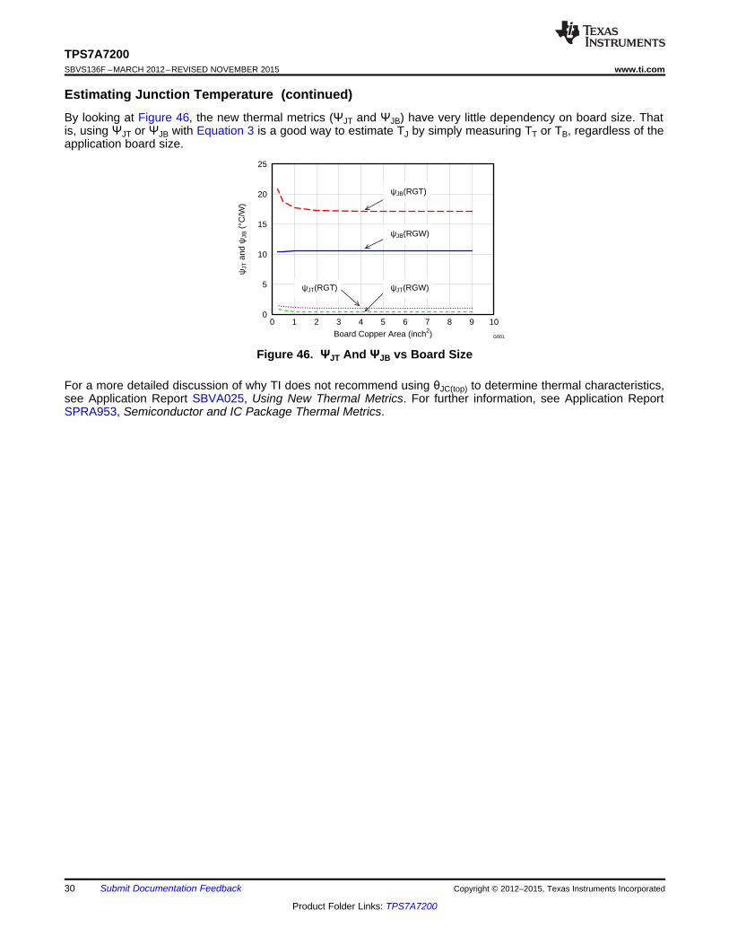
Estimating Junction Temperature (continued)By looking at Figure 46, the new thermal metrics (ΨJT and ΨJB) have very little dependency on board size. Thatis, using ΨJT or ΨJB with Equation 3 is a good way to estimate TJ by simply measuring TT or TB, regardless of theapplication board size.
Figure 46. ΨJT And ΨJB vs Board Size
For a more detailed discussion of why TI does not recommend using θJC(top) to determine thermal characteristics,see Application Report SBVA025, Using New Thermal Metrics. For further information, see Application ReportSPRA953, Semiconductor and IC Package Thermal Metrics.
31
TPS7A7200www.ti.com SBVS136F –MARCH 2012–REVISED NOVEMBER 2015
Product Folder Links: TPS7A7200
Submit Documentation FeedbackCopyright © 2012–2015, Texas Instruments Incorporated
11 Device And Documentation Support
11.1 Documentation Support
11.1.1 Related DocumentationFor related documentation see the following:• Pros and Cons of Using a Feedforward Capacitor with a Low-Dropout Regulator, SBVA042.• Using New Thermal Metrics, SBVA025.• TPS7A7x00EVM-718 Evaluation Module, SLAU430.• Semiconductor and IC Package Thermal Metrics, SPRA953.
11.2 Community ResourcesThe following links connect to TI community resources. Linked contents are provided "AS IS" by the respectivecontributors. They do not constitute TI specifications and do not necessarily reflect TI's views; see TI's Terms ofUse.
TI E2E™ Online Community TI's Engineer-to-Engineer (E2E) Community. Created to foster collaborationamong engineers. At e2e.ti.com, you can ask questions, share knowledge, explore ideas and helpsolve problems with fellow engineers.
Design Support TI's Design Support Quickly find helpful E2E forums along with design support tools andcontact information for technical support.
11.3 TrademarksDSP, E2E are trademarks of Texas Instruments.Bluetooth is a registered trademark of Bluetooth SIG, Inc.All other trademarks are the property of their respective owners.
11.4 Electrostatic Discharge CautionThese devices have limited built-in ESD protection. The leads should be shorted together or the device placed in conductive foamduring storage or handling to prevent electrostatic damage to the MOS gates.
11.5 GlossarySLYZ022 — TI Glossary.
This glossary lists and explains terms, acronyms, and definitions.
12 Mechanical, Packaging, And Orderable InformationThe following pages include mechanical, packaging, and orderable information. This information is the mostcurrent data available for the designated devices. This data is subject to change without notice and revision ofthis document. For browser-based versions of this data sheet, refer to the left-hand navigation.
PACKAGE OPTION ADDENDUM
www.ti.com 11-Aug-2017
Addendum-Page 1
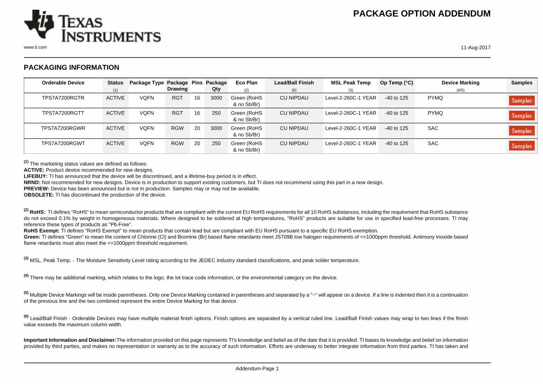
PACKAGING INFORMATION
Orderable Device Status(1)
Package Type PackageDrawing
Pins PackageQty
Eco Plan(2)
Lead/Ball Finish(6)
MSL Peak Temp(3)
Op Temp (°C) Device Marking(4/5)
Samples
TPS7A7200RGTR ACTIVE VQFN RGT 16 3000 Green (RoHS& no Sb/Br)
CU NIPDAU Level-2-260C-1 YEAR -40 to 125 PYMQ
TPS7A7200RGTT ACTIVE VQFN RGT 16 250 Green (RoHS& no Sb/Br)
CU NIPDAU Level-2-260C-1 YEAR -40 to 125 PYMQ
TPS7A7200RGWR ACTIVE VQFN RGW 20 3000 Green (RoHS& no Sb/Br)
CU NIPDAU Level-2-260C-1 YEAR -40 to 125 SAC
TPS7A7200RGWT ACTIVE VQFN RGW 20 250 Green (RoHS& no Sb/Br)
CU NIPDAU Level-2-260C-1 YEAR -40 to 125 SAC
(1) The marketing status values are defined as follows:ACTIVE: Product device recommended for new designs.LIFEBUY: TI has announced that the device will be discontinued, and a lifetime-buy period is in effect.NRND: Not recommended for new designs. Device is in production to support existing customers, but TI does not recommend using this part in a new design.PREVIEW: Device has been announced but is not in production. Samples may or may not be available.OBSOLETE: TI has discontinued the production of the device.
(2) RoHS: TI defines "RoHS" to mean semiconductor products that are compliant with the current EU RoHS requirements for all 10 RoHS substances, including the requirement that RoHS substancedo not exceed 0.1% by weight in homogeneous materials. Where designed to be soldered at high temperatures, "RoHS" products are suitable for use in specified lead-free processes. TI mayreference these types of products as "Pb-Free".RoHS Exempt: TI defines "RoHS Exempt" to mean products that contain lead but are compliant with EU RoHS pursuant to a specific EU RoHS exemption.Green: TI defines "Green" to mean the content of Chlorine (Cl) and Bromine (Br) based flame retardants meet JS709B low halogen requirements of <=1000ppm threshold. Antimony trioxide basedflame retardants must also meet the <=1000ppm threshold requirement.
(3) MSL, Peak Temp. - The Moisture Sensitivity Level rating according to the JEDEC industry standard classifications, and peak solder temperature.
(4) There may be additional marking, which relates to the logo, the lot trace code information, or the environmental category on the device.
(5) Multiple Device Markings will be inside parentheses. Only one Device Marking contained in parentheses and separated by a "~" will appear on a device. If a line is indented then it is a continuationof the previous line and the two combined represent the entire Device Marking for that device.
(6) Lead/Ball Finish - Orderable Devices may have multiple material finish options. Finish options are separated by a vertical ruled line. Lead/Ball Finish values may wrap to two lines if the finishvalue exceeds the maximum column width.
Important Information and Disclaimer:The information provided on this page represents TI's knowledge and belief as of the date that it is provided. TI bases its knowledge and belief on informationprovided by third parties, and makes no representation or warranty as to the accuracy of such information. Efforts are underway to better integrate information from third parties. TI has taken and
PACKAGE OPTION ADDENDUM
www.ti.com 11-Aug-2017
Addendum-Page 2
continues to take reasonable steps to provide representative and accurate information but may not have conducted destructive testing or chemical analysis on incoming materials and chemicals.TI and TI suppliers consider certain information to be proprietary, and thus CAS numbers and other limited information may not be available for release.
In no event shall TI's liability arising out of such information exceed the total purchase price of the TI part(s) at issue in this document sold by TI to Customer on an annual basis.
OTHER QUALIFIED VERSIONS OF TPS7A7200 :
• Enhanced Product: TPS7A7200-EP
NOTE: Qualified Version Definitions:
• Enhanced Product - Supports Defense, Aerospace and Medical Applications
TAPE AND REEL INFORMATION
*All dimensions are nominal
Device PackageType
PackageDrawing
Pins SPQ ReelDiameter
(mm)
ReelWidth
W1 (mm)
A0(mm)
B0(mm)
K0(mm)
P1(mm)
W(mm)
Pin1Quadrant
TPS7A7200RGTR VQFN RGT 16 3000 330.0 12.4 3.3 3.3 1.1 8.0 12.0 Q2
TPS7A7200RGTT VQFN RGT 16 250 180.0 12.4 3.3 3.3 1.1 8.0 12.0 Q2
TPS7A7200RGWR VQFN RGW 20 3000 330.0 12.4 5.3 5.3 1.1 8.0 12.0 Q2
TPS7A7200RGWT VQFN RGW 20 250 180.0 12.4 5.3 5.3 1.1 8.0 12.0 Q2
PACKAGE MATERIALS INFORMATION
www.ti.com 11-Aug-2017
Pack Materials-Page 1
*All dimensions are nominal
Device Package Type Package Drawing Pins SPQ Length (mm) Width (mm) Height (mm)
TPS7A7200RGTR VQFN RGT 16 3000 367.0 367.0 35.0
TPS7A7200RGTT VQFN RGT 16 250 210.0 185.0 35.0
TPS7A7200RGWR VQFN RGW 20 3000 367.0 367.0 35.0
TPS7A7200RGWT VQFN RGW 20 250 210.0 185.0 35.0
PACKAGE MATERIALS INFORMATION
www.ti.com 11-Aug-2017
Pack Materials-Page 2
www.ti.com
PACKAGE OUTLINE
C
16X 0.300.18
1.68 0.07
16X 0.50.3
1 MAX
(0.2) TYP
0.050.00
12X 0.5
4X1.5
A 3.12.9
B
3.12.9
VQFN - 1 mm max heightRGT0016CPLASTIC QUAD FLATPACK - NO LEAD
4222419/B 11/2016
PIN 1 INDEX AREA
0.08
SEATING PLANE
1
49
12
5 8
16 13
(OPTIONAL)PIN 1 ID 0.1 C A B
0.05
EXPOSEDTHERMAL PAD
SYMM
SYMM
NOTES: 1. All linear dimensions are in millimeters. Any dimensions in parenthesis are for reference only. Dimensioning and tolerancing per ASME Y14.5M. 2. This drawing is subject to change without notice. 3. The package thermal pad must be soldered to the printed circuit board for thermal and mechanical performance.
SCALE 3.600
www.ti.com
EXAMPLE BOARD LAYOUT
0.07 MINALL AROUND
0.07 MAXALL AROUND
16X (0.24)
16X (0.6)
( 0.2) TYPVIA
12X (0.5)
(2.8)
(2.8)
(0.58)TYP
( 1.68)
(R0.05)ALL PAD CORNERS
(0.58) TYP
VQFN - 1 mm max heightRGT0016CPLASTIC QUAD FLATPACK - NO LEAD
4222419/B 11/2016
SYMM
1
4
5 8
9
12
1316
SYMM
LAND PATTERN EXAMPLESCALE:20X
NOTES: (continued) 4. This package is designed to be soldered to a thermal pad on the board. For more information, see Texas Instruments literature number SLUA271 (www.ti.com/lit/slua271).5. Vias are optional depending on application, refer to device data sheet. If any vias are implemented, refer to their locations shown on this view. It is recommended that vias under paste be filled, plugged or tented.
SOLDER MASKOPENING
METAL UNDERSOLDER MASK
SOLDER MASKDEFINED
METAL
SOLDER MASKOPENING
SOLDER MASK DETAILS
NON SOLDER MASKDEFINED
(PREFERRED)
www.ti.com
EXAMPLE STENCIL DESIGN
16X (0.6)
16X (0.24)
12X (0.5)
(2.8)
(2.8)
( 1.55)
(R0.05) TYP
VQFN - 1 mm max heightRGT0016CPLASTIC QUAD FLATPACK - NO LEAD
4222419/B 11/2016
NOTES: (continued) 6. Laser cutting apertures with trapezoidal walls and rounded corners may offer better paste release. IPC-7525 may have alternate design recommendations.
SYMM
ALL AROUNDMETAL
SOLDER PASTE EXAMPLEBASED ON 0.125 mm THICK STENCIL
EXPOSED PAD 17:
85% PRINTED SOLDER COVERAGE BY AREA UNDER PACKAGESCALE:25X
SYMM
1
4
5 8
9
12
1316
17
IMPORTANT NOTICE
Texas Instruments Incorporated (TI) reserves the right to make corrections, enhancements, improvements and other changes to itssemiconductor products and services per JESD46, latest issue, and to discontinue any product or service per JESD48, latest issue. Buyersshould obtain the latest relevant information before placing orders and should verify that such information is current and complete.TI’s published terms of sale for semiconductor products (http://www.ti.com/sc/docs/stdterms.htm) apply to the sale of packaged integratedcircuit products that TI has qualified and released to market. Additional terms may apply to the use or sale of other types of TI products andservices.Reproduction of significant portions of TI information in TI data sheets is permissible only if reproduction is without alteration and isaccompanied by all associated warranties, conditions, limitations, and notices. TI is not responsible or liable for such reproduceddocumentation. Information of third parties may be subject to additional restrictions. Resale of TI products or services with statementsdifferent from or beyond the parameters stated by TI for that product or service voids all express and any implied warranties for theassociated TI product or service and is an unfair and deceptive business practice. TI is not responsible or liable for any such statements.Buyers and others who are developing systems that incorporate TI products (collectively, “Designers”) understand and agree that Designersremain responsible for using their independent analysis, evaluation and judgment in designing their applications and that Designers havefull and exclusive responsibility to assure the safety of Designers' applications and compliance of their applications (and of all TI productsused in or for Designers’ applications) with all applicable regulations, laws and other applicable requirements. Designer represents that, withrespect to their applications, Designer has all the necessary expertise to create and implement safeguards that (1) anticipate dangerousconsequences of failures, (2) monitor failures and their consequences, and (3) lessen the likelihood of failures that might cause harm andtake appropriate actions. Designer agrees that prior to using or distributing any applications that include TI products, Designer willthoroughly test such applications and the functionality of such TI products as used in such applications.TI’s provision of technical, application or other design advice, quality characterization, reliability data or other services or information,including, but not limited to, reference designs and materials relating to evaluation modules, (collectively, “TI Resources”) are intended toassist designers who are developing applications that incorporate TI products; by downloading, accessing or using TI Resources in anyway, Designer (individually or, if Designer is acting on behalf of a company, Designer’s company) agrees to use any particular TI Resourcesolely for this purpose and subject to the terms of this Notice.TI’s provision of TI Resources does not expand or otherwise alter TI’s applicable published warranties or warranty disclaimers for TIproducts, and no additional obligations or liabilities arise from TI providing such TI Resources. TI reserves the right to make corrections,enhancements, improvements and other changes to its TI Resources. TI has not conducted any testing other than that specificallydescribed in the published documentation for a particular TI Resource.Designer is authorized to use, copy and modify any individual TI Resource only in connection with the development of applications thatinclude the TI product(s) identified in such TI Resource. NO OTHER LICENSE, EXPRESS OR IMPLIED, BY ESTOPPEL OR OTHERWISETO ANY OTHER TI INTELLECTUAL PROPERTY RIGHT, AND NO LICENSE TO ANY TECHNOLOGY OR INTELLECTUAL PROPERTYRIGHT OF TI OR ANY THIRD PARTY IS GRANTED HEREIN, including but not limited to any patent right, copyright, mask work right, orother intellectual property right relating to any combination, machine, or process in which TI products or services are used. Informationregarding or referencing third-party products or services does not constitute a license to use such products or services, or a warranty orendorsement thereof. Use of TI Resources may require a license from a third party under the patents or other intellectual property of thethird party, or a license from TI under the patents or other intellectual property of TI.TI RESOURCES ARE PROVIDED “AS IS” AND WITH ALL FAULTS. TI DISCLAIMS ALL OTHER WARRANTIES ORREPRESENTATIONS, EXPRESS OR IMPLIED, REGARDING RESOURCES OR USE THEREOF, INCLUDING BUT NOT LIMITED TOACCURACY OR COMPLETENESS, TITLE, ANY EPIDEMIC FAILURE WARRANTY AND ANY IMPLIED WARRANTIES OFMERCHANTABILITY, FITNESS FOR A PARTICULAR PURPOSE, AND NON-INFRINGEMENT OF ANY THIRD PARTY INTELLECTUALPROPERTY RIGHTS. TI SHALL NOT BE LIABLE FOR AND SHALL NOT DEFEND OR INDEMNIFY DESIGNER AGAINST ANY CLAIM,INCLUDING BUT NOT LIMITED TO ANY INFRINGEMENT CLAIM THAT RELATES TO OR IS BASED ON ANY COMBINATION OFPRODUCTS EVEN IF DESCRIBED IN TI RESOURCES OR OTHERWISE. IN NO EVENT SHALL TI BE LIABLE FOR ANY ACTUAL,DIRECT, SPECIAL, COLLATERAL, INDIRECT, PUNITIVE, INCIDENTAL, CONSEQUENTIAL OR EXEMPLARY DAMAGES INCONNECTION WITH OR ARISING OUT OF TI RESOURCES OR USE THEREOF, AND REGARDLESS OF WHETHER TI HAS BEENADVISED OF THE POSSIBILITY OF SUCH DAMAGES.Unless TI has explicitly designated an individual product as meeting the requirements of a particular industry standard (e.g., ISO/TS 16949and ISO 26262), TI is not responsible for any failure to meet such industry standard requirements.Where TI specifically promotes products as facilitating functional safety or as compliant with industry functional safety standards, suchproducts are intended to help enable customers to design and create their own applications that meet applicable functional safety standardsand requirements. Using products in an application does not by itself establish any safety features in the application. Designers mustensure compliance with safety-related requirements and standards applicable to their applications. Designer may not use any TI products inlife-critical medical equipment unless authorized officers of the parties have executed a special contract specifically governing such use.Life-critical medical equipment is medical equipment where failure of such equipment would cause serious bodily injury or death (e.g., lifesupport, pacemakers, defibrillators, heart pumps, neurostimulators, and implantables). Such equipment includes, without limitation, allmedical devices identified by the U.S. Food and Drug Administration as Class III devices and equivalent classifications outside the U.S.TI may expressly designate certain products as completing a particular qualification (e.g., Q100, Military Grade, or Enhanced Product).Designers agree that it has the necessary expertise to select the product with the appropriate qualification designation for their applicationsand that proper product selection is at Designers’ own risk. Designers are solely responsible for compliance with all legal and regulatoryrequirements in connection with such selection.Designer will fully indemnify TI and its representatives against any damages, costs, losses, and/or liabilities arising out of Designer’s non-compliance with the terms and provisions of this Notice.
Mailing Address: Texas Instruments, Post Office Box 655303, Dallas, Texas 75265Copyright © 2017, Texas Instruments Incorporated