Embed Size (px)
Citation preview
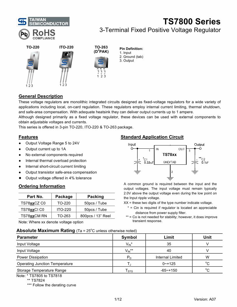
TS7800 Series 3-Terminal Fixed Positive Voltage Regulator
1/12 Version: A07
TO-220
ITO-220
TO-263 (D2PAK)
General Description These voltage regulators are monolithic integrated circuits designed as fixed-voltage regulators for a wide variety of applications including local, on-card regulation. These regulators employ internal current limiting, thermal shutdown, and safe-area compensation. With adequate heatsink they can deliver output currents up to 1 ampere. Although designed primarily as a fixed voltage regulator, these devices can be used with external components to obtain adjustable voltages and currents. This series is offered in 3-pin TO-220, ITO-220 & TO-263 package. Features ● Output Voltage Range 5 to 24V ● Output current up to 1A ● No external components required ● Internal thermal overload protection ● Internal short-circuit current limiting ● Output transistor safe-area compensation ● Output voltage offered in 4% tolerance
Ordering Information
Part No. Package Packing TS78xxCZ C0 TO-220 50pcs / Tube
TS78xxCI C0 ITO-220 50pcs / Tube TS78xxCM RN TO-263 800pcs / 13” Reel
Note: Where xx denote voltage option
Standard Application Circuit
Absolute Maximum Rating (Ta = 25oC unless otherwise noted) Parameter Symbol Limit Unit Input Voltage VIN* 35 V
Input Voltage VIN** 40 V
Power Dissipation PD Internal Limited W
Operating Junction Temperature TJ 0~+125 oC
Storage Temperature Range TSTG -65~+150 oC Note: * TS7805 to TS7818 ** TS7824 *** Follow the derating curve
A common ground is required between the input and the output voltages. The input voltage must remain typically 2.0V above the output voltage even during the low point on the Input ripple voltage. XX = these two digits of the type number indicate voltage.
* = Cin is required if regulator is located an appreciable distance from power supply filter.
** = Co is not needed for stability; however, it does improve transient response.
Pin Definition: 1. Input 2. Ground (tab) 3. Output
TS7800 Series 3-Terminal Fixed Positive Voltage Regulator
2/12 Version: A07
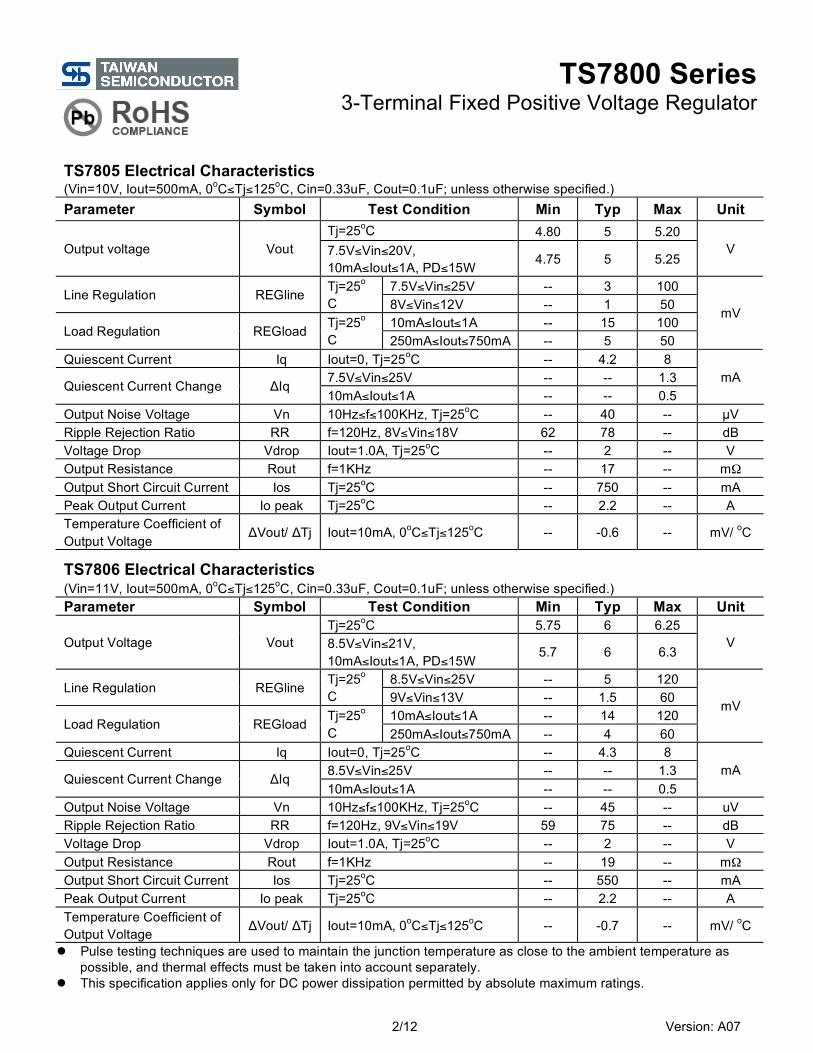
TS7805 Electrical Characteristics (Vin=10V, Iout=500mA, 0oC≤Tj≤125oC, Cin=0.33uF, Cout=0.1uF; unless otherwise specified.) Parameter Symbol Test Condition Min Typ Max Unit
Tj=25oC 4.80 5 5.20 Output voltage Vout 7.5V≤Vin≤20V,
10mA≤Iout≤1A, PD≤15W 4.75 5 5.25 V
7.5V≤Vin≤25V -- 3 100 Line Regulation REGline Tj=25o
C 8V≤Vin≤12V -- 1 50 10mA≤Iout≤1A -- 15 100 Load Regulation REGload Tj=25o
C 250mA≤Iout≤750mA -- 5 50
mV
Quiescent Current Iq Iout=0, Tj=25oC -- 4.2 8 7.5V≤Vin≤25V -- -- 1.3 Quiescent Current Change ΔIq 10mA≤Iout≤1A -- -- 0.5
mA
Output Noise Voltage Vn 10Hz≤f≤100KHz, Tj=25oC -- 40 -- µV Ripple Rejection Ratio RR f=120Hz, 8V≤Vin≤18V 62 78 -- dB Voltage Drop Vdrop Iout=1.0A, Tj=25oC -- 2 -- V Output Resistance Rout f=1KHz -- 17 -- mΩ Output Short Circuit Current Ios Tj=25oC -- 750 -- mA Peak Output Current Io peak Tj=25oC -- 2.2 -- A Temperature Coefficient of Output Voltage
ΔVout/ ΔTj Iout=10mA, 0oC≤Tj≤125oC -- -0.6 -- mV/ oC
TS7806 Electrical Characteristics (Vin=11V, Iout=500mA, 0oC≤Tj≤125oC, Cin=0.33uF, Cout=0.1uF; unless otherwise specified.) Parameter Symbol Test Condition Min Typ Max Unit
Tj=25oC 5.75 6 6.25 Output Voltage Vout 8.5V≤Vin≤21V,
10mA≤Iout≤1A, PD≤15W 5.7 6 6.3
V
8.5V≤Vin≤25V -- 5 120 Line Regulation REGline Tj=25o
C 9V≤Vin≤13V -- 1.5 60 10mA≤Iout≤1A -- 14 120 Load Regulation REGload Tj=25o
C 250mA≤Iout≤750mA -- 4 60
mV
Quiescent Current Iq Iout=0, Tj=25oC -- 4.3 8 8.5V≤Vin≤25V -- -- 1.3 Quiescent Current Change ΔIq 10mA≤Iout≤1A -- -- 0.5
mA
Output Noise Voltage Vn 10Hz≤f≤100KHz, Tj=25oC -- 45 -- uV Ripple Rejection Ratio RR f=120Hz, 9V≤Vin≤19V 59 75 -- dB Voltage Drop Vdrop Iout=1.0A, Tj=25oC -- 2 -- V Output Resistance Rout f=1KHz -- 19 -- mΩ Output Short Circuit Current Ios Tj=25oC -- 550 -- mA Peak Output Current Io peak Tj=25oC -- 2.2 -- A Temperature Coefficient of Output Voltage ΔVout/ ΔTj Iout=10mA, 0oC≤Tj≤125oC -- -0.7 -- mV/ oC
Pulse testing techniques are used to maintain the junction temperature as close to the ambient temperature as possible, and thermal effects must be taken into account separately.
This specification applies only for DC power dissipation permitted by absolute maximum ratings.

TS7800 Series 3-Terminal Fixed Positive Voltage Regulator
3/12 Version: A07
TS7808 Electrical Characteristics Vin=14V, Iout=500mA, 0oC≤Tj≤125oC, Cin=0.33uF, Cout=0.1uF; unless otherwise specified.) Parameter Symbol Test Condition Min Typ Max Unit
Tj=25oC 7.69 8 8.32 Output voltage Vout 10.5V≤Vin≤23V,
10mA≤Iout≤1A, PD≤15W 7.61 8 8.40 V
10.5V≤Vin≤25V -- 6 160 Line Regulation REGline Tj=25oC 11V≤Vin≤17V -- 2 80 10mA≤Iout≤1A -- 12 160 Load Regulation REGload Tj=25oC 250mA≤Iout≤750mA -- 4 80
mV
Quiescent Current Iq Iout=0, Tj=25oC -- 4.3 8 10.5V≤Vin≤25V -- -- 1 Quiescent Current Change ΔIq 10mA≤Iout≤1A -- -- 0.5
mA
Output Noise Voltage Vn 10Hz≤f≤100KHz, Tj=25oC -- 52 -- µV Ripple Rejection Ratio RR f=120Hz, 11V≤Vin≤21V 56 72 -- dB Voltage Drop Vdrop Iout=1.0A, Tj=25oC -- 2 -- V Output Resistance Rout f=1KHz -- 16 -- mΩ Output Short Circuit Current Ios Tj=25oC -- 450 -- mA Peak Output Current Io peak Tj=25oC -- 2.2 -- A Temperature Coefficient of Output Voltage ΔVout/ ΔTj Iout=10mA, 0oC≤Tj≤125oC -- -0.8 -- mV/ oC
TS7809 Electrical Characteristics (Vin=15V, Iout=500mA, 0oC≤Tj≤125oC, Cin=0.33uF, Cout=0.1uF; unless otherwise specified.) Parameter Symbol Test Condition Min Typ Max Unit
Tj=25oC 8.65 9 9.36 Output Voltage Vout 11.5V≤Vin≤23V,
10mA≤Iout≤1A, PD≤15W 8.57 9 9.45
V
11.5V≤Vin≤26V -- 6 180 Line Regulation REGline Tj=25oC 12V≤Vin≤17V -- 2 90 10mA≤Iout≤1A -- 12 180 Load Regulation REGload Tj=25oC 250mA≤Iout≤750mA -- 4 90
mV
Quiescent Current Iq Iout=0, Tj=25oC -- 4.3 8 11.5V≤Vin≤26V -- -- 1 Quiescent Current Change ΔIq 10mA≤Iout≤1A -- -- 0.5
mA
Output Noise Voltage Vn 10Hz≤f≤100KHz, Tj=25oC -- 52 -- uV Ripple Rejection Ratio RR f=120Hz, 12V≤Vin≤22V 55 72 -- dB Voltage Drop Vdrop Iout=1.0A, Tj=25oC -- 2 -- V Output Resistance Rout f=1KHz -- 16 -- mΩ Output Short Circuit Current Ios Tj=25oC -- 450 -- mA Peak Output Current Io peak Tj=25oC -- 2.2 -- A Temperature Coefficient of Output Voltage ΔVout/ ΔTj Iout=10mA, 0oC≤Tj≤125oC -- -1 -- mV/ oC
Pulse testing techniques are used to maintain the junction temperature as close to the ambient temperature as possible, and thermal effects must be taken into account separately.
This specification applies only for DC power dissipation permitted by absolute maximum ratings.
TS7800 Series 3-Terminal Fixed Positive Voltage Regulator
4/12 Version: A07
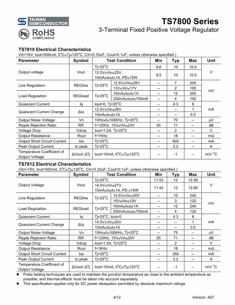
TS7810 Electrical Characteristics Vin=16V, Iout=500mA, 0oC≤Tj≤125oC, Cin=0.33uF, Cout=0.1uF; unless otherwise specified.) Parameter Symbol Test Condition Min Typ Max Unit
Tj=25oC 9.6 10 10.4 Output voltage Vout 12.5V≤Vin≤25V,
10mA≤Iout≤1A, PD≤15W 9.5 10 10.5 V
12.5V≤Vin≤28V -- 7 200 Line Regulation REGline Tj=25oC 13V≤Vin≤17V -- 2 100 10mA≤Iout≤1A -- 12 200 Load Regulation REGload Tj=25oC 250mA≤Iout≤750mA -- 4 100
mV
Quiescent Current Iq Iout=0, Tj=25oC -- 4.3 8 12.5V≤Vin≤28V -- -- 1 Quiescent Current Change ΔIq 10mA≤Iout≤1A -- -- 0.5
mA
Output Noise Voltage Vn 10Hz≤f≤100KHz, Tj=25oC -- 70 -- µV Ripple Rejection Ratio RR f=120Hz, 13V≤Vin≤23V 55 71 -- dB Voltage Drop Vdrop Iout=1.0A, Tj=25oC -- 2 -- V Output Resistance Rout f=1KHz -- 18 -- mΩ Output Short Circuit Current Ios Tj=25oC -- 400 -- mA Peak Output Current Io peak Tj=25oC -- 2.2 -- A Temperature Coefficient of Output Voltage
ΔVout/ ΔTj Iout=10mA, 0oC≤Tj≤125oC -- -1 -- mV/ oC
TS7812 Electrical Characteristics (Vin=19V, Iout=500mA, 0oC≤Tj≤125oC, Cin=0.33uF, Cout=0.1uF; unless otherwise specified.) Parameter Symbol Test Condition Min Typ Max Unit
Tj=25oC 11.53 12 12.48 Output Voltage Vout 14.5V≤Vin≤27V,
10mA≤Iout≤1A, PD ≤15W 11.42 12 12.60 V
14.5V≤Vin≤30V -- 10 240 Line Regulation REGline Tj=25oC 15V≤Vin≤19V -- 3 120 10mA≤Iout≤1A -- 12 240 Load Regulation REGload Tj=25oC 250mA≤Iout≤750mA -- 4 120
mV
Quiescent Current Iq Tj=25oC, Iout=0 -- 4.3 8 14.5V≤Vin≤30V -- -- 1 Quiescent Current Change ΔIq 10mA≤Iout≤1A -- -- 0.5
mA
Output Noise Voltage Vn 10Hz≤f≤100KHz, Tj=25oC -- 75 -- uV Ripple Rejection Ratio RR f=120Hz, 15V≤Vin≤25V 55 71 -- dB Voltage Drop Vdrop Iout=1.0A, Tj=25oC -- 2 -- V Output Resistance Rout f=1KHz -- 18 -- mΩ Output Short Circuit Current Ios Tj=25oC -- 350 -- mA Peak Output Current Io peak Tj=25oC -- 2.2 -- A Temperature Coefficient of Output Voltage ΔVout/ ΔTj Iout=10mA, 0oC≤Tj≤125oC -- -1 -- mV/ oC
Pulse testing techniques are used to maintain the junction temperature as close to the ambient temperature as possible, and thermal effects must be taken into account separately.
This specification applies only for DC power dissipation permitted by absolute maximum ratings.
TS7800 Series 3-Terminal Fixed Positive Voltage Regulator
5/12 Version: A07
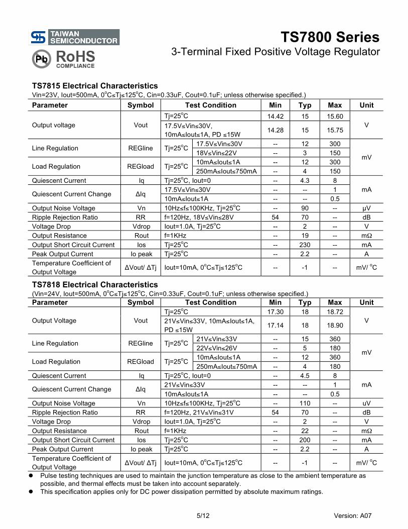
TS7815 Electrical Characteristics Vin=23V, Iout=500mA, 0oC≤Tj≤125oC, Cin=0.33uF, Cout=0.1uF; unless otherwise specified.) Parameter Symbol Test Condition Min Typ Max Unit
Tj=25oC 14.42 15 15.60 Output voltage Vout 17.5V≤Vin≤30V,
10mA≤Iout≤1A, PD ≤15W 14.28 15 15.75 V
17.5V≤Vin≤30V -- 12 300 Line Regulation REGline Tj=25oC 18V≤Vin≤22V -- 3 150 10mA≤Iout≤1A -- 12 300 Load Regulation REGload Tj=25oC 250mA≤Iout≤750mA -- 4 150
mV
Quiescent Current Iq Tj=25oC, Iout=0 -- 4.3 8 17.5V≤Vin≤30V -- -- 1 Quiescent Current Change ΔIq 10mA≤Iout≤1A -- -- 0.5
mA
Output Noise Voltage Vn 10Hz≤f≤100KHz, Tj=25oC -- 90 -- µV Ripple Rejection Ratio RR f=120Hz, 18V≤Vin≤28V 54 70 -- dB Voltage Drop Vdrop Iout=1.0A, Tj=25oC -- 2 -- V Output Resistance Rout f=1KHz -- 19 -- mΩ Output Short Circuit Current Ios Tj=25oC -- 230 -- mA Peak Output Current Io peak Tj=25oC -- 2.2 -- A Temperature Coefficient of Output Voltage
ΔVout/ ΔTj Iout=10mA, 0oC≤Tj≤125oC -- -1 -- mV/ oC
TS7818 Electrical Characteristics (Vin=24V, Iout=500mA, 0oC≤Tj≤125oC, Cin=0.33uF, Cout=0.1uF; unless otherwise specified.) Parameter Symbol Test Condition Min Typ Max Unit
Tj=25oC 17.30 18 18.72 Output Voltage Vout 21V≤Vin≤33V, 10mA≤Iout≤1A,
PD ≤15W 17.14 18 18.90
V
21V≤Vin≤33V -- 15 360 Line Regulation REGline Tj=25oC 22V≤Vin≤26V -- 5 180 10mA≤Iout≤1A -- 12 360 Load Regulation REGload Tj=25oC 250mA≤Iout≤750mA -- 4 180
mV
Quiescent Current Iq Tj=25oC, Iout=0 -- 4.5 8 21V≤Vin≤33V -- -- 1 Quiescent Current Change ΔIq 10mA≤Iout≤1A -- -- 0.5
mA
Output Noise Voltage Vn 10Hz≤f≤100KHz, Tj=25oC -- 110 -- uV Ripple Rejection Ratio RR f=120Hz, 21V≤Vin≤31V 54 70 -- dB Voltage Drop Vdrop Iout=1.0A, Tj=25oC -- 2 -- V Output Resistance Rout f=1KHz -- 22 -- mΩ Output Short Circuit Current Ios Tj=25oC -- 200 -- mA Peak Output Current Io peak Tj=25oC -- 2.2 -- A Temperature Coefficient of Output Voltage ΔVout/ ΔTj Iout=10mA, 0oC≤Tj≤125oC -- -1 -- mV/ oC
Pulse testing techniques are used to maintain the junction temperature as close to the ambient temperature as possible, and thermal effects must be taken into account separately.
This specification applies only for DC power dissipation permitted by absolute maximum ratings.
TS7800 Series 3-Terminal Fixed Positive Voltage Regulator
6/12 Version: A07
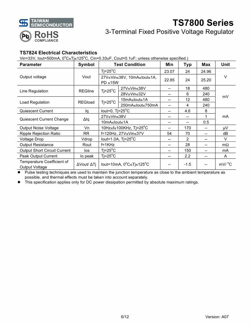
TS7824 Electrical Characteristics Vin=33V, Iout=500mA, 0oC≤Tj≤125oC, Cin=0.33uF, Cout=0.1uF; unless otherwise specified.) Parameter Symbol Test Condition Min Typ Max Unit
Tj=25oC 23.07 24 24.96 Output voltage Vout 27V≤Vin≤38V, 10mA≤Iout≤1A,
PD ≤15W 22.85 24 25.20 V
27V≤Vin≤38V -- 18 480 Line Regulation REGline Tj=25oC 28V≤Vin≤32V -- 6 240 10mA≤Iout≤1A -- 12 480 Load Regulation REGload Tj=25oC 250mA≤Iout≤750mA -- 4 240
mV
Quiescent Current Iq Iout=0, Tj=25oC -- 4.6 8 27V≤Vin≤38V -- -- 1 Quiescent Current Change ΔIq 10mA≤Iout≤1A -- -- 0.5
mA
Output Noise Voltage Vn 10Hz≤f≤100KHz, Tj=25oC -- 170 -- µV Ripple Rejection Ratio RR f=120Hz, 27V≤Vin≤37V 54 70 -- dB Voltage Drop Vdrop Iout=1.0A, Tj=25oC -- 2 -- V Output Resistance Rout f=1KHz -- 28 -- mΩ Output Short Circuit Current Ios Tj=25oC -- 150 -- mA Peak Output Current Io peak Tj=25oC -- 2.2 -- A Temperature Coefficient of Output Voltage
ΔVout/ ΔTj Iout=10mA, 0oC≤Tj≤125oC -- -1.5 -- mV/ oC
Pulse testing techniques are used to maintain the junction temperature as close to the ambient temperature as possible, and thermal effects must be taken into account separately.
This specification applies only for DC power dissipation permitted by absolute maximum ratings.
TS7800 Series 3-Terminal Fixed Positive Voltage Regulator
7/12 Version: A07
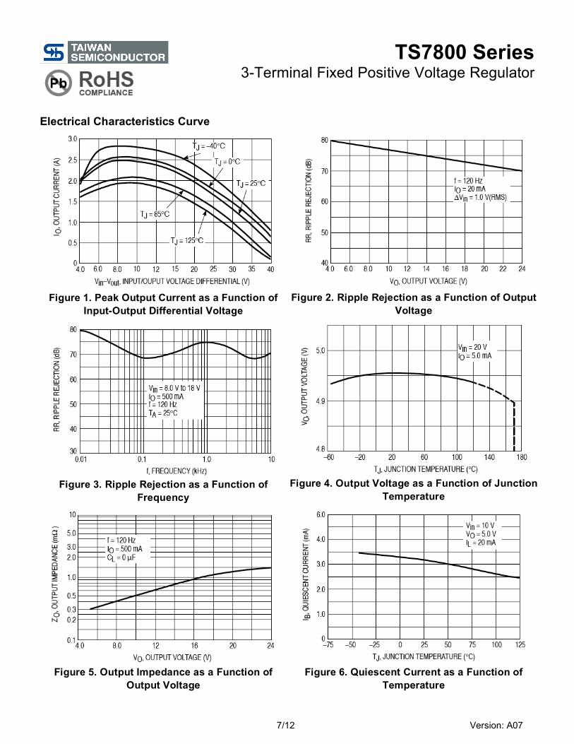
Electrical Characteristics Curve
Figure 1. Peak Output Current as a Function of
Input-Output Differential Voltage
Figure 2. Ripple Rejection as a Function of Output
Voltage
Figure 3. Ripple Rejection as a Function of
Frequency
Figure 4. Output Voltage as a Function of Junction
Temperature
Figure 5. Output Impedance as a Function of
Output Voltage
Figure 6. Quiescent Current as a Function of
Temperature
TS7800 Series 3-Terminal Fixed Positive Voltage Regulator
8/12 Version: A07
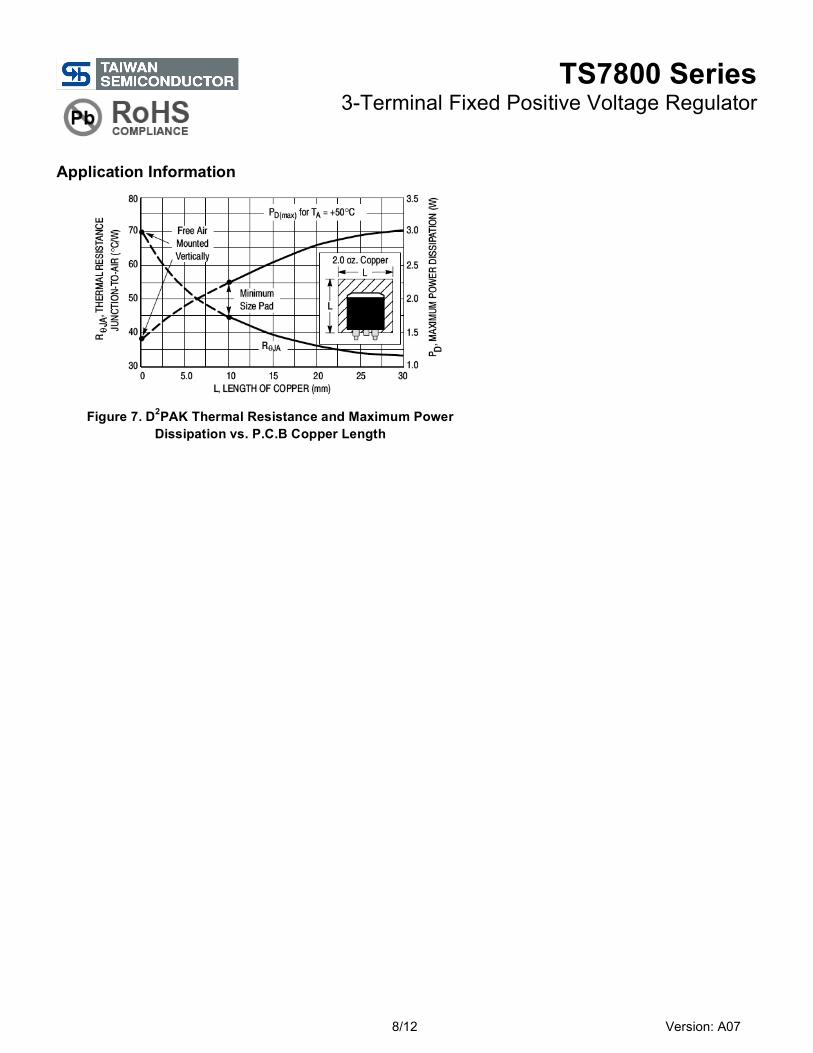
Application Information
Figure 7. D2PAK Thermal Resistance and Maximum Power
Dissipation vs. P.C.B Copper Length
TS7800 Series 3-Terminal Fixed Positive Voltage Regulator
9/12 Version: A07
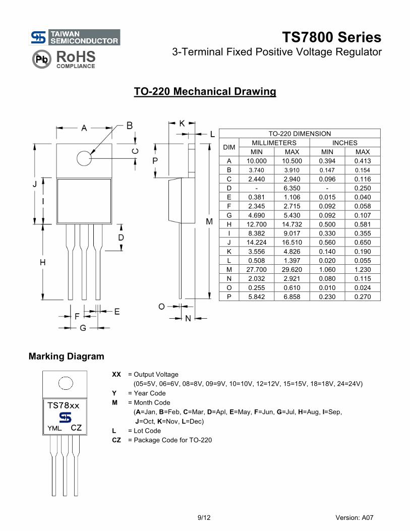
TO-220 Mechanical Drawing
Marking Diagram
XX = Output Voltage
(05=5V, 06=6V, 08=8V, 09=9V, 10=10V, 12=12V, 15=15V, 18=18V, 24=24V) Y = Year Code M = Month Code
(A=Jan, B=Feb, C=Mar, D=Apl, E=May, F=Jun, G=Jul, H=Aug, I=Sep, J=Oct, K=Nov, L=Dec)
L = Lot Code CZ = Package Code for TO-220
TO-220 DIMENSION MILLIMETERS INCHES DIM MIN MAX MIN MAX
A 10.000 10.500 0.394 0.413 B 3.740 3.910 0.147 0.154 C 2.440 2.940 0.096 0.116 D - 6.350 - 0.250 E 0.381 1.106 0.015 0.040 F 2.345 2.715 0.092 0.058 G 4.690 5.430 0.092 0.107 H 12.700 14.732 0.500 0.581 I 8.382 9.017 0.330 0.355 J 14.224 16.510 0.560 0.650 K 3.556 4.826 0.140 0.190 L 0.508 1.397 0.020 0.055 M 27.700 29.620 1.060 1.230 N 2.032 2.921 0.080 0.115 O 0.255 0.610 0.010 0.024 P 5.842 6.858 0.230 0.270
TS7800 Series 3-Terminal Fixed Positive Voltage Regulator
10/12 Version: A07
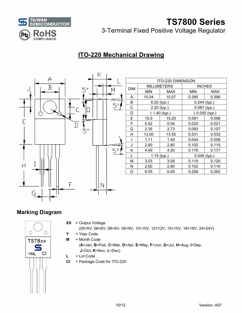
ITO-220 Mechanical Drawing
Marking Diagram
XX = Output Voltage
(05=5V, 06=6V, 08=8V, 09=9V, 10=10V, 12=12V, 15=15V, 18=18V, 24=24V) Y = Year Code M = Month Code
(A=Jan, B=Feb, C=Mar, D=Apl, E=May, F=Jun, G=Jul, H=Aug, I=Sep, J=Oct, K=Nov, L=Dec)
L = Lot Code CI = Package Code for ITO-220
ITO-220 DIMENSION MILLIMETERS INCHES DIM
MIN MAX MIN MAX A 10.04 10.07 0.395 0.396 B 6.20 (typ.) 0.244 (typ.) C 2.20 (typ.) 0.087 (typ.) D ∮1.40 (typ.) ∮0.055 (typ.) E 15.0 15.20 0.591 0.598 F 0.52 0.54 0.020 0.021 G 2.35 2.73 0.093 0.107 H 13.50 13.55 0.531 0.533 I 1.11 1.49 0.044 0.058 J 2.60 2.80 0.102 0.110 K 4.49 4.50 0.176 0.177 L 1.15 (typ.) 0.045 (typ.) M 3.03 3.05 0.119 0.120 N 2.60 2.80 0.102 0.110 O 6.55 6.65 0.258 0.262
TS7800 Series 3-Terminal Fixed Positive Voltage Regulator
11/12 Version: A07
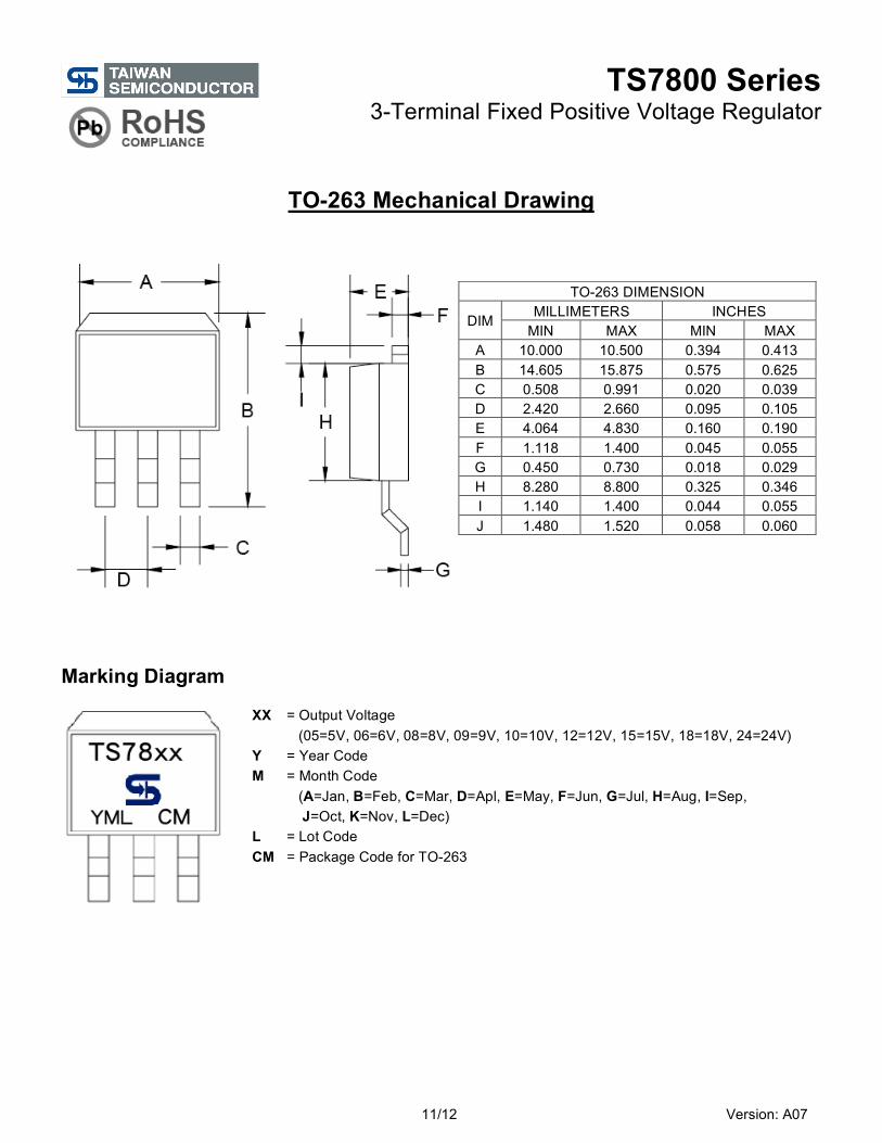
TO-263 Mechanical Drawing
Marking Diagram
XX = Output Voltage
(05=5V, 06=6V, 08=8V, 09=9V, 10=10V, 12=12V, 15=15V, 18=18V, 24=24V) Y = Year Code M = Month Code
(A=Jan, B=Feb, C=Mar, D=Apl, E=May, F=Jun, G=Jul, H=Aug, I=Sep, J=Oct, K=Nov, L=Dec)
L = Lot Code CM = Package Code for TO-263
TO-263 DIMENSION MILLIMETERS INCHES DIM
MIN MAX MIN MAX A 10.000 10.500 0.394 0.413 B 14.605 15.875 0.575 0.625 C 0.508 0.991 0.020 0.039 D 2.420 2.660 0.095 0.105 E 4.064 4.830 0.160 0.190 F 1.118 1.400 0.045 0.055 G 0.450 0.730 0.018 0.029 H 8.280 8.800 0.325 0.346 I 1.140 1.400 0.044 0.055 J 1.480 1.520 0.058 0.060
TS7800 Series 3-Terminal Fixed Positive Voltage Regulator
12/12 Version: A07
Notice Specifications of the products displayed herein are subject to change without notice. TSC or anyone on its behalf, assumes no responsibility or liability for any errors or inaccuracies. Information contained herein is intended to provide a product description only. No license, express or implied, to any intellectual property rights is granted by this document. Except as provided in TSC’s terms and conditions of sale for such products, TSC assumes no liability whatsoever, and disclaims any express or implied warranty, relating to sale and/or use of TSC products including liability or warranties relating to fitness for a particular purpose, merchantability, or infringement of any patent, copyright, or other intellectual property right. The products shown herein are not designed for use in medical, life-saving, or life-sustaining applications. Customers using or selling these products for use in such applications do so at their own risk and agree to fully indemnify TSC for any damages resulting from such improper use or sale.


![THE - Technea · DC input power [W] Max. PV voltage [V] Rated input voltage [V] ... 160-280. 12 13 ... Emergence Power Supply](https://img.pdfslide.net/doc/110x75/5af0cece7f8b9aa17b8f75b7/the-technea-input-power-w-max-pv-voltage-v-rated-input-voltage-v-160-280.jpg)


![051224 - Nipron€¦ · 051224 - 2 - Model ePCSA-500P-X2S Item Line Regulation V3:12V 18A at AC Input at AC Input Input Voltage [V] Output Voltage [V] Fluctuation Value](https://img.pdfslide.net/doc/110x75/5ac754ee7f8b9acb7c8bccf9/051224-nipron-051224-2-model-epcsa-500p-x2s-item-line-regulation-v312v.jpg)