Embed Size (px)
Citation preview

Tutorial:
Introduction to FPGA design
with Xilinx ISE 13
and prototyping boards
Juan A. Gómez-Pulido
Departament of Technologies of Computers and Communications
University of Extremadura, Spain
(c) 2012
Version: 1/october/2011

Tutorial: Introduction to FPGA design with Xilinx ISE 13 and prototyping boards.
2
Table of contents. 1. Introduction ......................................................................................................................................................... 3
1.1.1. Purpose. ............................................................................................................................................... 3 1.1.2. Tools. .................................................................................................................................................. 3 1.1.3. Sources and documents. ...................................................................................................................... 3
2. System design ...................................................................................................................................................... 4 2.1. Modeling a 1-bit adder. ................................................................................................................................ 4
2.1.1. Creating the project “sumacon8”. ....................................................................................................... 4 2.1.2. Creating the “sum1” object by means of schematic. ........................................................................... 5
2.2. Functional simulation. ................................................................................................................................. 6 2.2.1. Simulating using VHDL Test Bench. ................................................................................................. 6
2.3. Modeling and functional simulation of an 8-bit adder. ................................................................................ 7 2.3.1. Creating the “sum1” symbol. .............................................................................................................. 7 2.3.2. Creating the 8-bit adder. ...................................................................................................................... 7
2.4. Counter modelled from Core Generator .................................................................................................... 10 3. Implementation .................................................................................................................................................. 12
3.1. Preparing the circuit. .................................................................................................................................. 12 3.1.1. Introduction. ...................................................................................................................................... 12 3.1.2. Planning the system. ......................................................................................................................... 12 3.1.3. Buses connector. ............................................................................................................................... 12 3.1.4. Building the memories. ..................................................................................................................... 13 3.1.5. Decoding the sum. ............................................................................................................................. 14 3.1.6. Using the 7-segment display. ............................................................................................................ 16 3.1.7. Final circuit. ...................................................................................................................................... 17
3.2. Implementation and test. ............................................................................................................................ 18 3.2.1. Assigning FPGA pins. ....................................................................................................................... 18 3.2.2. Assigning pins in the schematic sheet. .............................................................................................. 19 3.2.3. Assigning pins by means of the user constraints files (UCF). ........................................................... 19 3.2.4. Implementation. ................................................................................................................................ 19 3.2.5. FPGA layout. .................................................................................................................................... 20 3.2.6. Implementation reports. .................................................................................................................... 20 3.2.7. Testing the design with the board. .................................................................................................... 21
4. Other models for the system .............................................................................................................................. 22 4.1. Counter designed from flip-flops. .............................................................................................................. 22 4.2. Counter modeled from the Picoblaze processor. ........................................................................................ 24
4.2.1. Counter design. ................................................................................................................................. 25 4.2.2. Final design. ...................................................................................................................................... 26 4.2.3. Implementation. ................................................................................................................................ 27
5. Documents ......................................................................................................................................................... 28 5.1. General Considerations and Frequently Asked Questions. ........................................................................ 28
5.1.1. Errores durante la síntesis e implementación. ................................................................................... 28 5.1.2. Errores en el diseño del proyecto: ..................................................................................................... 28
5.2. Nexys / Nexys2 boards. ............................................................................................................................. 28 5.2.1. Manuals. ............................................................................................................................................ 28 5.2.2. Initial checking. ................................................................................................................................. 28 5.2.3. FPGA configuration. ......................................................................................................................... 29 5.2.4. Pins for Nexys. .................................................................................................................................. 29 5.2.5. Pins for Nexys2. ................................................................................................................................ 30 5.2.6. Clock in Nexys. ................................................................................................................................. 30

Introduction
3
1. Introduction
1.1.1. Purpose.
This lab introduces the student in the use of tools and platforms for reconfigurable computing. The following steps implement the typical phases of the design cycle: idea, modeling, simulation, synthesis and implementation, time analysis, prototyping and debugging.
Considerations:
All variable names will be displayed within quotation marks (“”).
1.1.2. Tools.
Xilinx ISE 13 software environment.
Xilinx PicoBlaze for Spartan3 libraries and software.
A prototyping board: Digilent Nexys, Nexys2.
USB cable.
Using other prototyping boards: This lab can be easily adapted to be used with other prototyping boards, if the following issues are taken into account:
The I/O FPGA pins must be correctly mapped to the DIP and LED devices in the board.
The used FPGA must have libraries with the common elements used in this lab.
1.1.3. Sources and documents.
Some source files, manuals and documents are required along this tutorial. These resources will be provided by the instructor.

Tutorial: Introduction to FPGA design with Xilinx ISE 13 and prototyping boards.
4
2. System design
2.1. Modeling a 1-bit adder.
A full 1-bit adder (from now on, “sum1”) is a logic circuit that adds three bits ("A", "B" and "Ci", where "A" and "B" are the source bits and "Ci" ("i" from "input") is the input carry bit from a previous add stage) and produces the add bit "S" and the output carry bit "Co" ("o" from "out"). The truth table of "S" and "Co" bits of the 1-bit adder is:
A B Ci S Co 0 0 0 0 0 0 0 1 1 0 0 1 0 1 0 0 1 1 0 1 1 0 0 1 0 1 0 1 0 1 1 1 0 0 1 1 1 1 1 1
"S" and "Co" can be expressed such as the following sum of minterms:
S = !A·!B·Ci + !A·B·!Ci + A·!B·!Ci + A·B·Ci
Co = !A·B·Ci+A·!B·Ci+A·B·!Ci+A·B·Ci
The "S" and "Co" functions can be simplified to:
S = A $ B $ Ci
Co = A·B + B·Ci + A·Ci
where $ means exclusive-OR (XOR). This is the explanation: S = !A·!B·Ci + !A·B·!Ci + A·!B·!Ci + A·B·Ci = Ci·(!A·!B + A·B) + !Ci·(!A·B + A·!B) = = Ci·(A xnor B) + !Ci·(A xor B) = Ci·!(A xor B) + !Ci·(A xor B) = (A xor B) xor Ci
“Co” could not be reduced by Karnaugh: Co = A·B + B·Ci + A·Ci
Also, we can demonstrate that: Co = !A·B·Ci+A·!B·Ci+A·B·!Ci+A·B·Ci =....= A·B+B·Ci+A·Ci
2.1.1. Creating the project “sumacon8”.
Start Xilinx ISE environment clicking in the "project navigator" icon. In "File" -> "New project" select the project name, "sumacon8", the working folder (the selected path should not have white spaces, for example, “C:\iseprojects\sumacon8”) and the high-level design type as "schematic". This means that the highest design level will be a schematic sheet showing the different components, some of them enclosing other designs (lower levels).
Next, we specify the FPGA where the design is going to be implemented (ask your instructor which the board is). Select your board in the field "Evaluation development board". If your board doesn't appear in this field, select manually the FPGA characteristics according to the following table:

System design
5
Board FPGA Family Device Package Speed Nexys-1000 Spartan3E XC3S1000 FT256 -4 Nexys2-500 Spartan3E XC3S500E FG320 -4 Nexys2-1200 Spartan3E XC3S1200E FG320 -4
Check if the other selections are "Schematic - XST - XST (VHDL/Verilog) - ISim(VHDL/Verilog) - VHDL - Store all values". Press "Next" to finish.
2.1.2. Creating the “sum1” object by means of schematic.
We are going to model a 1-bit adder with the schematic tools given. In the “Sources for Implementation” window, we create the “sum1” sheet clicking the right mouse button on the window, or in the "Project" -> "New source" menu. Select the "Schematic" type and put "sum1" as file name in the working folder. This sheet is added to the project and the schematic editor is opened. In order to facilitate the editing of the circuit, we recommend to select “float” if you right-click on the “sum1.sch” tab at the bottom of the sheet window.
To create the circuit, we can use the figure below, placing 3 "AND2" gates, 2 "OR2", 2 "XOR2", 3 1-bit input markers (for the "a", "b" and "ci" signals) and 2 1-bit output markers (for the "s" and "co" signals). We can use the “Add” menu or the icons of the drawing tools. You can read the integrated help to see the drawing sheet procedures. Once the circuit is created, we check it has not errors by means of "Tools" -> "Check Schematic". If there are not errors, we save the sheet and close the schematic editor.

Tutorial: Introduction to FPGA design with Xilinx ISE 13 and prototyping boards.
6
2.2. Functional simulation.
We have to check the required behavior of the 1-bit adder before create the symbol “sum1”. There are two possible ways in ISE 13: from a “waveform” or “VHDL Test Bench”.
2.2.1. Simulating using VHDL Test Bench.
In the “Dessign” tab, select the “Simulation” option.
"Project" -> "New source" -> Create the "testbench_sum1" file of type "VHDL Test Bench" -> "Next" -> Select the "sum1" schematic sheet to indicate that the simulation we are going to do is linked to the model described in that sheet -> "Next" -> "Finish".
A VHDL code appears. We use this code to select the values of the signals along the time in the way shown in the figure below. For this and future tasks, read "Writing Efficient Testbenches" (http://arco.unex.es/resources/xapp199.pdf).
Replace the section “Test Bench - User Defined Section” with the code shown below. Save it.
LIBRARY ieee; USE ieee.std_logic_1164.ALL; USE ieee.numeric_std.ALL; LIBRARY UNISIM; USE UNISIM.Vcomponents.ALL; ENTITY sum1_sum1_sch_tb IS END sum1_sum1_sch_tb; ARCHITECTURE behavioral OF sum1_sum1_sch_tb IS COMPONENT sum1 PORT( a : IN STD_LOGIC; b : IN STD_LOGIC; ci : IN STD_LOGIC; s : OUT STD_LOGIC; co : OUT STD_LOGIC); END COMPONENT; SIGNAL a : STD_LOGIC; SIGNAL b : STD_LOGIC; SIGNAL ci : STD_LOGIC; SIGNAL s : STD_LOGIC; SIGNAL co: STD_LOGIC; BEGIN UUT: sum1 PORT MAP( a => a, b => b, ci => ci, s => s, co => co ); -- *** Test Bench - User Defined Section *** tb : PROCESS BEGIN
a <= '0'; b <= '0'; ci <= '0'; WAIT for 200 ns; a <= '1'; WAIT for 200 ns; a <= '0'; b <= '1'; WAIT for 200 ns; a <= '1'; WAIT for 200 ns; a <= '0'; b <= '0'; ci <= '1'; WAIT for 200 ns; a <= '1'; WAIT for 200 ns; a <= '0'; b <= '1'; WAIT for 200 ns; a <= '1'; WAIT for 200 ns; a <= '0'; b <= '0'; ci <= '0'; WAIT; -- will wait forever END PROCESS; -- *** End Test Bench - User Defined Section *** END;

System design
7
Next, check the code by means of "Behavioral Check Syntax". Debug errors if any. Then, right-click "Run" on "Simulate Behavioral Model" to perform the simulation.
Check if the waveform result corresponds with the image below (use the "Zoom-in" and "Zoom-out" icons, and the slide bar at the bottom side to adjust the simulation waveform to the window).
2.3. Modeling and functional simulation of an 8-bit adder.
2.3.1. Creating the “sum1” symbol.
Our purpose now is to create a symbol (a hardware object) with the name “sum1”, to be included in the project library. This way we can use, for example, several 1-bit adders in other schematic sheet avoiding repeating many times the last designed circuit, just including the “sum1” symbol from the project library, because this symbol acts as a 1-bit adder.
The way to create the “sum1” symbol and to store in the symbols library is the following: select the “sum1.sch” sheet in the "Implementation" view -> select "Create Schematic Symbol" under the "Design Utilities" category in the "Processes: sum1” window -> right-click and execute “Run”.
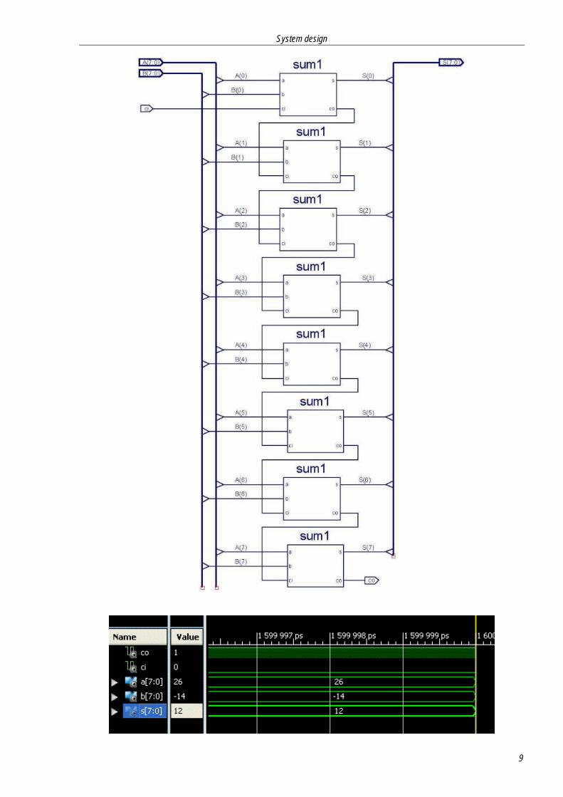
2.3.2. Creating the 8-bit adder.
We want to model now a circuit that adds two 8-bit input signals (buses “A” and “B”) taking into account an input carry. This adder produces the sum (an 8-bit output signal) and an output carry. You can use the integrated help to see how to draw the circuit elements.

Tutorial: Introduction to FPGA design with Xilinx ISE 13 and prototyping boards.
8
Create a new schematic sheet named "sum8.sch".
Select the symbol “sum1” in the window “Symbols" (icon “Add symbol”). This symbol is located in the category "<c:\...>" (symbols placed in our working folder).
Place in a serial array 8 “sum1” symbols, for example in a column so they fit in the sheet (if they don’t fit in the sheet, you can change the sheet size or edit the draw of the symbol to reduce its size -on the symbol, click the right mouse button -> "Symbol" -> "Edit Symbol"-).
Connect the output carry of the first 1-bit adder to the input carry of the next 1-bit adder, etc.
The sheet must contain the I/O markers for the signals "A(7:0)" ,"B(7:0)", "S(7:0)", "Cin" and "Cout". To do it, we will draw buses for the operands, the result and the carry connections.
Draw the bus for the sum using "Add Wire" to draw a long vertical connection near to the add output signals (but without connect to them). We place a I/O marker in the end of the bus (appearing a default name) using "Add I/O Marker". Clicking on this name we change it to "S(7:0)",so this 1-bit wire becomes into the 8-bit bus "S". We check this bus has the output direction. We repeat this operation to build the input buses "A(7:0)" and "B(7:0)" Also, we place I/O marker to the input carry signal "Ci" and to the output carry signal “Co".
Next, connect the 1-bit adders to the corresponding buses. For example, to conect the outputs:
o “Add Wire" -> in the window "Options", select "Use the autorouter to add...." and "automatically add a bus tap...." -> conect the 1-bit adder output to the bus.
o Repeat for all the adders output signals.
o Naming the nets: "Add Net Name" -> in the window "Options", select "Name the branch", put in "Name" the value "S(0)", activate "Display the name ...", and select "Increment the name..." ->The cursor with the legend "S(0)" appears, then we put it on the net between the first 1-bit adder (above) and the bus -> Click -> We see the net is named with "S(0)" and the cursor points now to "S(1)", in order to be applied to the next net, and so on.
Next, check there are not errors in the schematic using the "Check Schematic" button. A window with the errors and warnings appears. If all is OK, the message says "No errors detected".
Generate the symbol "sum8" to be used in the future in the top level sheet.
Finally, we are going to do a functional simulation in order to check the correct behaviour of the circuit:
"Project" -> "New source" -> build the file "test_sum8" of type "VHDL Test Bench" -> "Next" -> Select the schematic sheet "sum8" to indicate that the simulation we are going to do is related to the described model in that sheet -> "Next" -> "Finish".
The VHDL code appears. Put the required statements (between “BEGIN” and “WAIT;”) in order to:
o Maintain “Cin” equal to 0.
o Set the "1A" and "F2" hexadecimal values (for example) to the buses "A" and "B" respectively.
Check the syntax.
Save the code.
Select the “Simulation” view in the “Design” tab -> select "test_sum8" in the behavioral hierarchy -> go to the "Processes" window -> expand “ISim Simulator" -> right-click “Run” on "Simulate Behavioral Model".
Chek if the result is correct (you can use the "Radix" option to change the way the values on the waveform are shown, right-clicking on the proper signal). It is convenient to probe different ways to assign values and see the results in order to check the proper behavior of the adder.
System design
9

Tutorial: Introduction to FPGA design with Xilinx ISE 13 and prototyping boards.
10
2.4. Counter modelled from Core Generator
We are going to supply the operands to the adder with a counter generated from the Xilinx Core Generator tool. This tool generates some configurable components using a wizard. These components are known as "IP cores" (IP from "Intellectual Property").
Knowing that there will be a future synthesis of the circuit for a specific prototyping board, we must to take into account this counter will loop the 16 addresses of two memories containing the operands of the adder. The produced sums will be shown in 7-segment displays. The counter will produce their outputs in each clock cycle (around 100 MHz with the onboard clock), so it is impossible to see the successive results to this speed. Therefore, we will build a 30-bit counter (generating 2^30= 1 Giga of outputs) instead of a 4-bit counter (generating the 16 addresses). We will use the 4 most significative bits (“4 msb”) of the 30-bit counter to generate the 16 addresses, so:
100 MHz --> 1 cycle = 10^-8 s
2^30 = 1 Gcycles --> 1 G * 10^-8 sec = 10,7 sec = time to go through the 16 addresses of the memories using the 4 msb.
We will proceed in this way to build the counter:
"Project" -> "New Source" -> Select "IP (Core Generator & Architecture Wizard)" with name "contador30" -> “Next” -> Coregen opens; select "Basic Elements" -> "Counters" -> "Binary Counter" -> "Next" -> "Finish".
A wizard appears, where we select output width 30 bits and operation mode "up/down". We generate this counter and its symbol associated clicking on the button "Generate".
Create a new schematic sheet: "top_ip.sch".
Place the symbol "contador30" (note it is located in a different folder under the current working folder).
Attach and the corresponding I/O markers (up, clk, q(29:0)).
Check with "Check Schematic" that all is OK and exit from the schematic editor.
Simulate the counter: "Project" -> "New Source" -> build "test_top_ip" as "VHDL Test Bench" -> assign it to the sheet "top_ip".

System design
11
Use the generated VHDL code to customize the simulation:
o At the beginning, assign 0 to "up", and a clock signal to "clk" with period of 100 ns.
o Assign "1" to "up" at 400 ns.
o Assign "0" to "up" again after passed 1000 ns.
LIBRARY ieee; USE ieee.std_logic_1164.ALL; USE ieee.numeric_std.ALL; LIBRARY UNISIM; USE UNISIM.Vcomponents.ALL; ENTITY top_ip_top_ip_sch_tb IS END top_ip_top_ip_sch_tb; ARCHITECTURE behavioral OF top_ip_top_ip_sch_tb IS COMPONENT top_ip PORT( up : IN STD_LOGIC; clk : IN STD_LOGIC; q : OUT STD_LOGIC_VECTOR (29 DOWNTO 0)); END COMPONENT; SIGNAL up : STD_LOGIC; SIGNAL clk : STD_LOGIC; SIGNAL q : STD_LOGIC_VECTOR (29 DOWNTO 0); CONSTANT ClockPeriod : TIME := 100 ns; BEGIN UUT: top_ip PORT MAP( up => up, clk => clk, q => q );
-- *** Test Bench - User Defined Section *** PROCESS BEGIN clk <= '0'; wait for ClockPeriod/2; clk <= '1'; wait for ClockPeriod/2; END PROCESS; tb : PROCESS BEGIN up <= '0'; WAIT FOR 400 ns; up <= '1'; WAIT FOR 1000 ns; up <= '0'; WAIT; -- will wait forever END PROCESS; -- *** End Test Bench - User Defined Section *** END;
Check the syntax to debug errors.
We want to end the simulation at time 1600 ns, so before performing simulation we do: “simulation” view -> Select the module "test_top_ip" in the hierarchy -> go to the window "Processes" -> select "Simulate Behavioral Model", click right-button and select "Process properties" and change "Simulation Run Time" to 1600 ns.
Run the simulation.
Check the proper behavior of the system. Look at the figure below. Select the format “signed decimal” for the output signal.

Tutorial: Introduction to FPGA design with Xilinx ISE 13 and prototyping boards.
12
3. Implementation
3.1. Preparing the circuit.
3.1.1. Introduction.
In this section we are going to implement the circuit on a FPGA. The circuit needs to be adapted for implementing, because the I/O signals must match to the prototyping board characteristics where the FPGA is mounted.
3.1.2. Planning the system.
The final system is going to supply the operands to the adder through the contents of two ROM memories, which addresses are generated with the counter implemented with "Core Generator".
Besides building the two memories, we need build a device connecting the 30-bit bus in the adder output to the 4-bit buses in the input of the memories.
3.1.3. Buses connector.
"Project" -> "New Source" -> “VHDL module” with name "contador30_4msb" -> 30-bit input "Qin", 4-bit output "Qout" -> The file "contador30_4msb.vhd" is built.
Copy in the architecture section of the VHDL file the code shown below.
library IEEE; use IEEE.STD_LOGIC_1164.ALL; use IEEE.STD_LOGIC_ARITH.ALL; use IEEE.STD_LOGIC_UNSIGNED.ALL; ------------- entity contador30_4msb is Port ( Qin : in std_logic_vector(29 downto 0); Qout : out std_logic_vector(3 downto 0)); end contador30_4msb; ------------- architecture Behavioral of contador30_4msb is begin process(Qin) begin Qout(3 downto 0) <= Qin(29 downto 26); end process; end Behavioral;
Check the syntax.
Create the symbol "contador30_4msb".

Implementation
13
Place it in the schematic sheet “top_ip”, connecting its input to the counter output.
3.1.4. Building the memories.
The ROM memories will have 16 words of 8-bit wide, so we can supply any of them as operands of the adder, selecting the addresses cyclically. Start creating the ROM that supplies values to the first operand “A” of the adder.
"Project" -> "New source" -> "IP (CoreGen)" with name "rom_a" -> "Memories & storage elements" -> "RAMs & ROMs" -> "Block Memory Generator" (select the latest version) -> "Finish".
The "Core Generator" tool with the Block Memory Generator appears. In the successive pages, select the following parameters (maintaining the other options with their default values): "Single Port ROM" and "Minimum Area" (page 2); "Read Width"=8 and "Read Depth"=16 (page 3) -> "Generate".
This way the symbol "rom_a" is built, which we can use in the schematic sheet "top_ip". Repeat this procedure to create “rom_b” with the same characteristics.
Now, we need to define the ROM content. This content is defined in a ".coe" file that can be written in any ASCII editor. We want the following contents for both memories, expressed like unsigned integer words, from the lowest to the highest address:
rom_a: {0, 2, 3, 8, 116, 255, 155, 255, 0, 1, 2, 3, 1, 2, 3, 4}
rom_b: {0, 3, 7, 102, 94, 55, 255, 255, 1, 2, 3, 4, 0, 1, 2, 3}
These are the contents for the files (copy-paste the content of the box for the corresponding file):
rom_a.coe:
rom_b.coe:
MEMORY_INITIALIZATION_RADIX=10; MEMORY_INITIALIZATION_VECTOR= 0, 2, 3, 8, 116, 255, 155, 255, 0, 1, 2, 3, 1, 2, 3, 4;
MEMORY_INITIALIZATION_RADIX=10; MEMORY_INITIALIZATION_VECTOR= 0, 3, 7, 102, 94, 55, 255, 255, 1, 2, 3, 4, 0, 1, 2, 3;
Once both files have been created in the working folder, they must be included in the ROMs cores following these steps:
Select "rom_a" in the window “Hierarchy” in the "Implementation” view in the “Design” Tab.
Go to "Processes" -> "CORE generator" -> "Manage Cores" – “Run” -> The "coregen" window appears.
Select the "rom_a" core in the left-bottom window and then, select "Recustomize and Generate (under current project settings)" in the right side or right-clicking the mouse.
The "Block Memory Generator" wizard appears again. Click "Next" until the page 4.
Activate the "Load Init File" option -> select the "rom_a.coe" file for the “Coe File” field -> press "Generate".
Repeat the same actions for "rom_b" (in this case, select “rom_b.coe”).
Close the "coregen" window.

Tutorial: Introduction to FPGA design with Xilinx ISE 13 and prototyping boards.
14
Next, place the memories on the sheet "top_ip", connect the clock signal (in the counter input) to the clock inputs of the memories, and connect the "contador30_4msb" output to the addresses inputs of the memories. Assign the I/O markers and check there are not errors in the schematic sheet.
3.1.5. Decoding the sum.
Take into account that the adder result will take a value in the range 0 to 255, with a carry 0 or 1, so:
If Co = 0 then 0 <= S <= 255
If Co = 1 thent 256 <= S <= 510
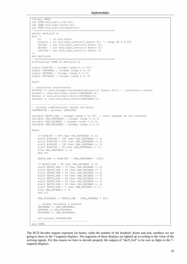
Therefore, first we built a BCD decoder that converts the adder result (8-bit array with the output carry) into the corresponding numbers for hundred, dozen and unit, separated in order to be shown in the displays of the prototyping board (Nexys):
"Project" -> "New Source" -> “VHDL module” with name "dec9_bcd" -> 1-bit input "Co", 8-bit input "binario", 4-bit outputs "unidad", "decena" y "centena", and put “COMB" as the architecture name (instead of "Behavioral") -> The file "dec9_bcd.vhd" is built.
Copy the code shown below into the architecture section of the code.
Check and create the symbol "dec9_bcd".
Implementation
15
library IEEE; use IEEE.std_logic_1164.all; use IEEE.std_logic_arith.all; use IEEE.std_logic_unsigned.all; --===================================================== entity dec9_bcd is port ( Co : in std_logic; binario : in std_logic_vector(7 downto 0); -- rango de 0 a 255 unidad : out std_logic_vector(3 downto 0); decena : out std_logic_vector(3 downto 0); centena : out std_logic_vector(3 downto 0) ); end dec9_bcd; --===================================================== architecture COMB of dec9_bcd is signal BIN2INT : integer range 0 to 511; signal CENTENAS : integer range 0 to 5; signal DECENAS : integer range 0 to 9; signal UNIDADES : integer range 0 to 9; begin -- sentencias concurrentes BIN2INT <= conv_integer(unsigned(Co&binario(7 downto 0))); -- convierte a entero unidad <= conv_std_logic_vector(UNIDADES,4); decena <= conv_std_logic_vector(DECENAS,4); centena <= conv_std_logic_vector(CENTENAS,3); ------------------------------------- -- proceso combinacional usando variables CONVERSION : process (BIN2INT) variable RES99_VAR : integer range 0 to 99; -- resto después de las centenas variable VAR_CENTENAS : integer range 0 to 5; variable VAR_DECENAS : integer range 0 to 9; variable VAR_UNIDADES : integer range 0 to 9; begin if BIN2INT > 499 then VAR_CENTENAS := 5; elsif BIN2INT > 399 then VAR_CENTENAS := 4; elsif BIN2INT > 299 then VAR_CENTENAS := 3; elsif BIN2INT > 199 then VAR_CENTENAS := 2; elsif BIN2INT > 99 then VAR_CENTENAS := 1; else VAR_CENTENAS := 0; end if; RES99_VAR := BIN2INT - (VAR_CENTENAS * 100); if RES99_VAR > 89 then VAR_DECENAS := 9; elsif RES99_VAR > 79 then VAR_DECENAS := 8; elsif RES99_VAR > 69 then VAR_DECENAS := 7; elsif RES99_VAR > 59 then VAR_DECENAS := 6; elsif RES99_VAR > 49 then VAR_DECENAS := 5; elsif RES99_VAR > 39 then VAR_DECENAS := 4; elsif RES99_VAR > 29 then VAR_DECENAS := 3; elsif RES99_VAR > 19 then VAR_DECENAS := 2; elsif RES99_VAR > 9 then VAR_DECENAS := 1; else VAR_DECENAS := 0; end if; VAR_UNIDADES := RES99_VAR - (VAR_DECENAS * 10); -- asigna variables a señales CENTENAS <= VAR_CENTENAS; DECENAS <= VAR_DECENAS; UNIDADES <= VAR_UNIDADES; end process CONVERSION; ------------------------------------- end COMB;
The BCD decoder outputs represent (in binary code) the number of the hundred, dozen and unit, numbers we are going to show in the 7-segment displays. The segments of these displays are lighted up according to the value of the arriving signals. For this reason we have to decode properly the outputs of "dec9_bcd" to be own as digits in the 7-segment displays.

Tutorial: Introduction to FPGA design with Xilinx ISE 13 and prototyping boards.
16
3.1.6. Using the 7-segment display.
We will need two modules to decode the hundred, dozen and unit and to show them in the 7-segment displays:
Module "displays_controller":
o "Project" -> "New Source" -> VHDL module with name "displays_controller" -> 1-bit input "mclk" and 4-bit inputs "digitU", "digitD" and "digitC"; 4-bit outputs "digit" and "display_enable" -> The file "displays_controller.vhd" is built.
o We paste into the architecture section of the code the copied piece of code shown in the figure. This code takes into account how the sequence of the signals activating the four displays must be produced, according to the manual of the Nexys board.
o Build the symbol "displays_controller”.
library IEEE; use IEEE.STD_LOGIC_1164.ALL; use IEEE.STD_LOGIC_ARITH.ALL; use IEEE.STD_LOGIC_UNSIGNED.ALL; --================================================= entity displays_controller is Port ( mclk : in STD_LOGIC; digitU : in STD_LOGIC_VECTOR (3 downto 0); digitD : in STD_LOGIC_VECTOR (3 downto 0); digitC : in STD_LOGIC_VECTOR (3 downto 0); digit : out STD_LOGIC_VECTOR (3 downto 0); display_enable : out STD_LOGIC_VECTOR (3 downto 0) ); end displays_controller; --================================================= architecture Behavioral of displays_controller is signal cont : integer range 0 to 4 := 0; signal clkdiv : std_logic_vector(10 downto 0); signal clk : std_logic; begin display_enable <= "1110" when cont = 0 else "1101" when cont = 1 else "1011" when cont = 2 else "1111" when cont = 3 else "1111"; digit <= digitU when cont = 0 else digitD when cont = 1 else digitC when cont = 2 else "0000"; -- Divido la frequencia de reloj para obtener una más baja process (mclk) begin if mclk = '1' and mclk'Event then clkdiv <= clkdiv + 1; end if; end process; clk <= clkdiv(10); process(clk) begin if clk = '1' and clk'Event then if cont >= 3 then cont <= 0; else cont <= cont+1; end if; end if; end process; end Behavioral;
Module "decbcd":
o "Project" -> "New Source" -> VHDL module with name "decbcd" -> 4-bit input "HEX" and 7-bit output "LED" -> The file "decbcd.vhd" is built.

Implementation
17
o We paste into the architecture section of the code the copied piece of code shown in the figure. This code takes into account the numbering order of the display segments, according to the manual of the Nexys board.
o Build the symbol "decled".
library IEEE; use IEEE.STD_LOGIC_1164.ALL; use IEEE.STD_LOGIC_ARITH.ALL; use IEEE.STD_LOGIC_UNSIGNED.ALL; --================================================= entity decbcd is Port( HEX : in std_logic_vector(3 downto 0); LED : out std_logic_vector(6 downto 0) ); end decbcd; --================================================= architecture Behavioral of decbcd is signal segs : std_logic_vector(6 downto 0); begin -- 0 -- --- -- 5 | | 1 -- --- <- 6 -- 4 | | 2 -- --- -- 3 with HEX SELect segs <= "0111111" when "0000", --0 "0000110" when "0001", --1 "1011011" when "0010", --2 "1001111" when "0011", --3 "1100110" when "0100", --4 "1101101" when "0101", --5 "1111101" when "0110", --6 "0000111" when "0111", --7 "1111111" when "1000", --8 "1101111" when "1001", --9 "1110111" when "1010", --A "1111100" when "1011", --b "0111001" when "1100", --C "1011110" when "1101", --d "1111001" when "1110", --E "1110011" when "1111", --F "0000000" when others; --(nada) LED <= not segs; end Behavioral;
3.1.7. Final circuit.
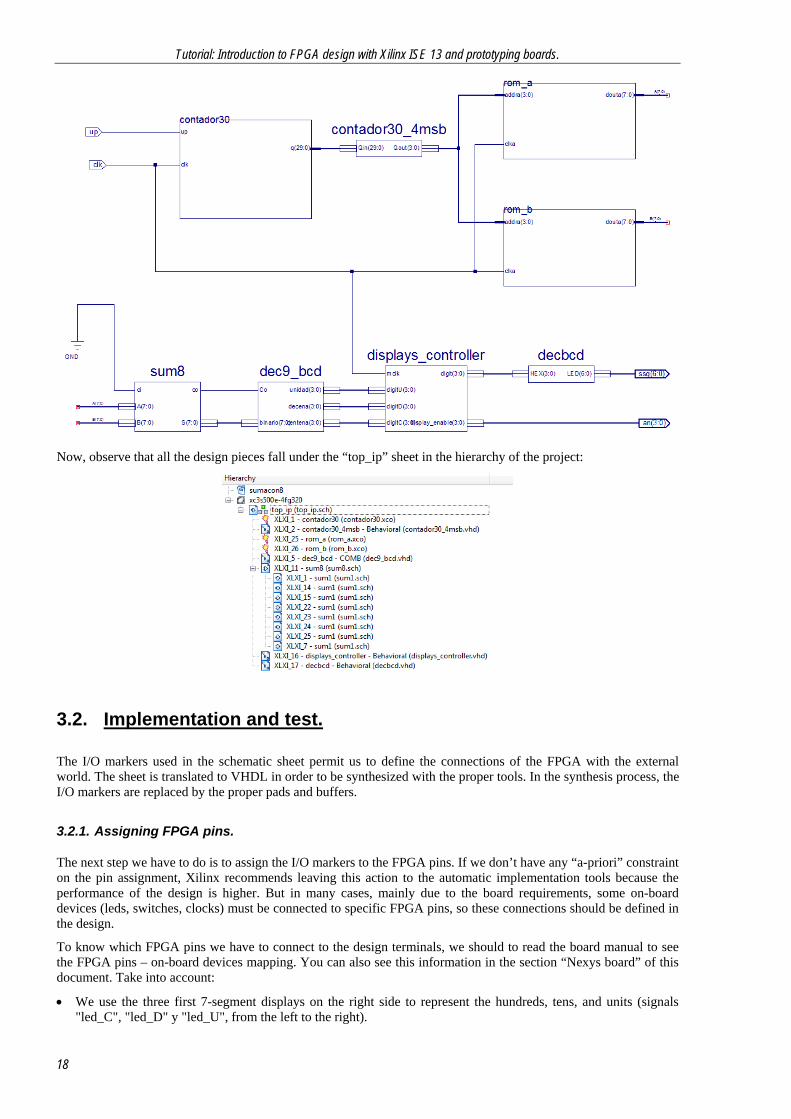
Place the symbols "sum8", "dec9_bcd", "displays_controller" and "decbcd" in the schematic sheet "top_ip", as it is indicated in the figure.
Place a ground connection to the input signal "ci" of the symbol "sum8".
Put an output marker “ssg(6:0)” to the “LED” output of the symbols "decbcd" and
Put an output marker “an(3:0) to the output "display_enable(3:0)" of the symbol "displays_controller".
Check the sheet does not contain errors.
Tutorial: Introduction to FPGA design with Xilinx ISE 13 and prototyping boards.
18
Now, observe that all the design pieces fall under the “top_ip” sheet in the hierarchy of the project:
3.2. Implementation and test.
The I/O markers used in the schematic sheet permit us to define the connections of the FPGA with the external world. The sheet is translated to VHDL in order to be synthesized with the proper tools. In the synthesis process, the I/O markers are replaced by the proper pads and buffers.
3.2.1. Assigning FPGA pins.
The next step we have to do is to assign the I/O markers to the FPGA pins. If we don’t have any “a-priori” constraint on the pin assignment, Xilinx recommends leaving this action to the automatic implementation tools because the performance of the design is higher. But in many cases, mainly due to the board requirements, some on-board devices (leds, switches, clocks) must be connected to specific FPGA pins, so these connections should be defined in the design.
To know which FPGA pins we have to connect to the design terminals, we should to read the board manual to see the FPGA pins – on-board devices mapping. You can also see this information in the section “Nexys board” of this document. Take into account:
We use the three first 7-segment displays on the right side to represent the hundreds, tens, and units (signals "led_C", "led_D" y "led_U", from the left to the right).

Implementation
19
We use the clock signal from the on-board oscillator (100 MHz) to supply the signal “clk” to the design inside the FPGA.
We use the SW0 switch to change the value of the signal "up".
There are two ways to do the pin assignment:
3.2.2. Assigning pins in the schematic sheet.
This method assigns the pin in the schematic by means of the attribute “LOC”. In this lab we are going to skip this method in benefit of a more flexible method.
3.2.3. Assigning pins by means of the user constraints files (UCF).
Assign the inputs "clk" and "up", and the outputs "an" and "ssg", creating a plain text UCF file:
"Project" -> "New Source" -> "Implementation Constraints File", type "sumacon8_ip" -> "Next" -> select "top_ip" -> "Next" -> "Finish". The empty file "sumacon8_ip.ucf" has been created.
Select "sumacon8_ip.ucf" in the hierarchy view of the project -> run the process "Edit Constraints (Text)" under "User Constraints" in the window "Processes" -> The file opens itself -> paste the following sentences:
Nexys-1000 Nexys2-500 Nexys2-1200 NET "up" LOC = "N15"; NET "an<0>" LOC = "G14"; NET "an<1>" LOC = "G12"; NET "an<2>" LOC = "G13"; NET "an<3>" LOC = "F12"; NET "ssg<0>" LOC = "F13"; NET "ssg<1>" LOC = "E13"; NET "ssg<2>" LOC = "G15"; NET "ssg<3>" LOC = "H13"; NET "ssg<4>" LOC = "J14"; NET "ssg<5>" LOC = "E14"; NET "ssg<6>" LOC = "G16"; NET "clk" LOC = "A8";
NET "up" LOC = "G18"; NET "an<0>" LOC = "F17"; NET "an<1>" LOC = "H17"; NET "an<2>" LOC = "C18"; NET "an<3>" LOC = "F15"; NET "ssg<0>" LOC = "L18"; NET "ssg<1>" LOC = "F18"; NET "ssg<2>" LOC = "D17"; NET "ssg<3>" LOC = "D16"; NET "ssg<4>" LOC = "G14"; NET "ssg<5>" LOC = "J17"; NET "ssg<6>" LOC = "H14"; NET "clk" LOC = "B8";
NET "up" LOC = "G18"; NET "an<0>" LOC = "F17"; NET "an<1>" LOC = "H17"; NET "an<2>" LOC = "C18"; NET "an<3>" LOC = "F15"; NET "ssg<0>" LOC = "L18"; NET "ssg<1>" LOC = "F18"; NET "ssg<2>" LOC = "D17"; NET "ssg<3>" LOC = "D16"; NET "ssg<4>" LOC = "G14"; NET "ssg<5>" LOC = "J17"; NET "ssg<6>" LOC = "H14"; NET "clk" LOC = "B8";
3.2.4. Implementation.
We are going to proceed to make the full implementation:
Select "top_ip" in the "Design"-“Implementation” view.
Go to "Processes" -> Select "Implement Design" -> Right-click -> "Process Properties" -> Expand to “Advanced” in the “Property display level” field, and then check "Perform Advanced Analysis" in the category "Post-Place & Route Static Timing Report Properties" -> OK.

Tutorial: Introduction to FPGA design with Xilinx ISE 13 and prototyping boards.
20
Select "Generate Programming File" -> "Process Properties" -> Select "JTAG Clock" in the field "FPGA Start-Up Clock" in the category "Startup Options" -> OK.
Select "Generate Programming File" -> "Run". The implementation process begins. After few minutes, the different implementation processes end: "Synthesize", "Translate", "Map", "Place" and "Route". Finally, the "top_ip.bit" file is generated, ready to configure the FPGA.
3.2.5. FPGA layout.
We can see the layout of the design in the FPGA using the tool "FPGA Editor":
Go to “Processes” -> Run "View/Edit Routed Design (FPGA Editor)" in the category "Place & Route" in the process "Implement Design".
In "FPGA Editor", select “All Nets” in the window "List" to see any net of the design. Select the signal “clk" and see how it is placed in the FPGA.
3.2.6. Implementation reports.
During the implementation, there is interesting information generated. In the window “Design Summary” a summary of some results is shown.
Open the window "Design Summary" running "View Design Summary" in "Processes".
See that only the 1% of the FPGA logic resources (occupied slices) is used.
In the sub-window "FPGA Design Summary" -> "Detailed Reports" -> "Static Timing Reports" -> See near the end of this file that the maximum frequency for which this circuit can operate accurately is 206 MHz (this value can vary depending on the board and the implementation).

Implementation
21
3.2.7. Testing the design with the board.
Test the design following the configuration procedure described in the "Nexys/Nexys2 board" section at the end of this document. After configuring it, see how the displays show the sequence of the figure below. Drive the switch SW0 and see how the sequence is inverted.

Tutorial: Introduction to FPGA design with Xilinx ISE 13 and prototyping boards.
22
4. Other models for the system
4.1. Counter designed from flip-flops.
In this section, the student will replace the 30-bit counter used in the current design (sheet "top_ip.sch") by a finite state machine modeled by means of 30 registers using D-type flip-flops processing in parallel. We can start from a new project, or use the current project and modules already designed. We choose the second option:
“Project” -> “Cleanup project files”.
Save the current top sheet "top_ip.sch" as "top_fds.sch"(open the sheet -> “File” –> “Save as”).
In the current project only one top sheet must exist, so go to the project tree, select “top_ip” sheet and remove it from the project (“Sources” -> ”Remove”).
Add the file “top_fds.sch” to the design (“Project” -> ”Add source”).
Save the user constraints file "sumacon8_ip.ucf" as "sumacon8_fds.ucf". Remove the first from the project and add the second.
Open the top sheet. Delete the symbol “contador30". In the space left we’ll place the new counter. Close the sheet.
See in the project tree that the "contador30.xco" module appears at the same level as the top sheet. This means that this counter is out of the top sheet and it doesn’t be longer used, so you should remove it from the project.
The new counter, based on a finite-state machine implemented with flip-flops, follows the typical scheme of the Mealy’s machine:
This scheme has two modules: the FSM consisting of a set of registers, and a controller that increases or decreases the output sequence. So, in the "top_fds" sheet we will have:
Other models for the system
23
Take into account that we have now an additional input: "reset". This signal permits reinitialize the counter at any time. So, we should add a new pin specification for the “reset” signal in the constraints file "sumacon8_fds.ucf" (use the on-board switch SW1 because SW0 is reserved for “up” signal).
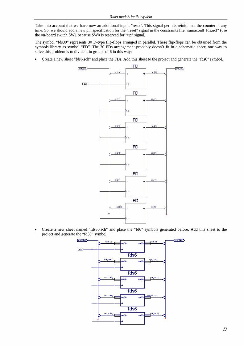
The symbol “fds30” represents 30 D-type flip-flops arranged in parallel. These flip-flops can be obtained from the symbols library as symbol “FD”. The 30 FDs arrangement probably doesn’t fit in a schematic sheet; one way to solve this problem is to divide it in groups of 6 in this way:
Create a new sheet “fds6.sch" and place the FDs. Add this sheet to the project and generate the "fds6" symbol.
Create a new sheet named "fds30.sch" and place the “fd6" symbols generated before. Add this sheet to the project and generate the “fd30” symbol.

Tutorial: Introduction to FPGA design with Xilinx ISE 13 and prototyping boards.
24
Finally, the increaser will be the following VHDL code (incrementador.vhd):
library IEEE; use IEEE.STD_LOGIC_1164.ALL; use IEEE.STD_LOGIC_ARITH.ALL; use IEEE.STD_LOGIC_UNSIGNED.ALL; entity incrementador is Port ( up : in std_logic; reset : in std_logic; cst : in std_logic_vector(29 downto 0); nst : out std_logic_vector(29 downto 0)); end incrementador; architecture Behavioral of incrementador is begin process(reset,up,cst) begin if reset='1' then nst <= "000000000000000000000000000000"; else if up='1' then nst <= cst+1; else nst <= cst-1; end if; end if; end process; end Behavioral;
The final project should be something like this:
Finally, the constraints file must be modified. Add to the UCF file the line corresponding to the signal “reset”, which should be controlled by means of the switch SW1 on the Nexys board. See the last section of this document to know what the FPGA pin is.
Simulate, implement (generate the "top_fds.bit" configuration file) and probe the system in the board. The result should be the same, plus an additional feature: the reset switch permits to reinitialize the counter. Check it.
4.2. Counter modeled from the Picoblaze processor.
We're going to design the same counter using the embedded processor Picoblaze. You can know more about this microprocessor taking a look to these documents (you can find them in http://arco.unex.es/resources):
KCPSM - Constant(k) Coded Programmable State Machine.
PicoBlaze 8-Bit Microcontroller for Virtex Devices.
Start from the current project and modules already designed instead of creating a new one:
Save the current top sheet "top_fds.sch" as "top_pico.sch" (open the sheet -> “File” –> “Save as”).
In the current project only one top sheet must exist, so remove “top_fds” and add “top_pico” to the design.
Save the user constraints file "sumacon8_ip.ucf" as "sumacon8_fds.ucf". Remove the first from the project and add the second.
Open the top sheet. Remove only the counter (including the module "contador30_4msb"). In the space left we’ll place the new counter. Close the sheet.
You can see in the project tree that the modules "incrementador", "contador30_4msb", "fds30" and "fd6" appear at the same level as the top sheet, so remove them from the project.

Other models for the system
25
4.2.1. Counter design.
The counter will be implemented by means of an assembler code for the microprocessor "picoblaze". This processor is embedded in the design by means of the module "kcpsm" generated from the file "kcpsm.vhd". Thanks to its instruction set, we can create the assembler code "prog.psm" to program a counter. This code is placed in the design as a memory module from the VHDL code "prog.vhd" generated.
Create a void schematic sheet named "cont_pico.sch" and add it to the project.
Add to the project the file "kcpsm.vhd", generate its symbol and add it to this schematic sheet.
With these actions we have placed the processor in the design. Now we must add the program that this processor will run.
Create and edit a plain-text file named “prog.psm" with this content:
; 8 BITS COUNTER CONSTANT byte, ff ; 8 bits counter CONSTANT zero, 00 ; clear regs CONSTANT event_port, 02 ; puerto entrada (bit0 será el dato) start: LOAD sA, zero ; sets counter to 0 in sA display: OUTPUT sA, byte ; outputs counter value CALL delay INPUT s0, event_port ; reads the input AND s0, 01 ; analyze bit0 JUMP Z, dec ; if yes, go to dec inc: ADD sA, 01 ; increments the counter JUMP display dec: SUB sA, 01 ; decrements the counter JUMP display ;software delay loop - apprx 1 second at 40MHz clock delay: LOAD s2, 98 outer_dly: LOAD s3, FF middle_dly: LOAD s4, FF inner_dly: SUB s4, 01 JUMP NZ, inner_dly SUB s3, 01 JUMP NZ, middle_dly SUB s2, 01 JUMP NZ, outer_dly RETURN
Copy the files "kcpsm.exe", "ROM_form.vhd" and "ROM_form.coe" to the project folder (download them from
the resources web page).
Run "KCPSM prog.psm" in a command-line window, for example, with the "System symbol” utility of MS Windows. The file "prog.vhd" is generated. Add it to the project, generate its symbol and place it in the schematic sheet "cont_pico.sch", connecting it to the processor as you can see in the figure.

Tutorial: Introduction to FPGA design with Xilinx ISE 13 and prototyping boards.
26
The processor accepts input data and produce output data. We need an associated circuit to process these data, as you can see in the following figure. Due to its complexity, you can skip the effort using the schematic sheet “circuito_adicional” to build the circuit (but it would be good if you try to do it yourself).
Once finished the circuit “cont_pico”, generate its symbol.
4.2.2. Final design.
Place the symbol “cont_pico” in the sheet "top_pico.sch", with the corresponding nets as shown in this figure:

Other models for the system
27
When checking this schematic, ignore the 7 warnings saying "Net 'data(...)' is connected to load pins and/or I/O markers, but not connected to any source pin or I/O marker". This means these 7 signals are not connected, but it doesn't affect to the circuit operation.
The final project tree should be like this:
4.2.3. Implementation.
We will use the first switch (SW0) to establish the up/down counter direction (signal "up"). This signal is the first bit (the less significant) of the input "data(7:0)" of the counter. In addition, we will use the second switch (SW1) to enable the counter, so we must to set this switch such “reset”=1 (switch down).
We will not use the signals “interrupt” and “strobe”.
Edit the UCF file to add/modify the proper sentences.
Generate the configuration file "top_pico.bit", download it to the FPGA and check the board operation.

Tutorial: Introduction to FPGA design with Xilinx ISE 13 and prototyping boards.
28
5. Documents
5.1. General Considerations and Frequently Asked Questions.
5.1.1. Errores durante la síntesis e implementación.
Generalmente, los informes de errores y avisos durante este proceso nos pueden dar una pista de la causa del error. No obstante, estas son las causas más habituales:
A veces se producen errores durante la síntesis e implementación debido a la no actualización de los componentes del diseño (hojas de esquemas, símbolos, códigos VHDL e IP cores). Esto suele suceder habitualmente cuando guardamos todo el proyecto en un medio extraible para volver a grabarlo posteriormente en cualquier equipo. La solución es:
o En la ventana "Sources" , seleccionamos con el ratón la parte más superior del árblo del diseño, donde aparece el nombre del mismo (por encima del tipo de FPGA seleccionado).
o En la ventana "Processes", expandimos la categoría "Design Utilities".
o Ejecutamos "Regenerate All Coress".
o Ejecutamos "Update All Schematic Files".
Las señales en el diseño no se corresponden con las señales en el archivo UCF.
El diseño es demasiado grande para la FPGA seleccionada.
5.1.2. Errores en el diseño del proyecto:
En el árbol del proyecto no aparece un elemento, o aparece con una interrogación. Si lo añadimos, sale un mensaje de error avisando que ya está en el proyecto:
o En la ventana "Sources", ir a la pestaña "Libraries".
o Expandir la categoría "Work".
o Localizar el elemento en cuestión, y borrarlo (botón derecho del ratón, y "Remove").
o Volver a la ventana "Sources", volver a añadir el elemento mediante "Add Source".
Para hacer una limpieza de archivos no necesarios que pueden provocar algún problema: "Project" -> "Cleanup Project Files".
5.2. Nexys / Nexys2 boards.
5.2.1. Manuals.
Get and read the full users manuals of the boards at http://arco.unex.es/resources. Following you can see the more basic information about these boards.
5.2.2. Initial checking.
Keep on mind these actions before testing your designs:
The board must be configured with the blue jumpers in these places:
o For nexys:
JP3 in JTAG position.
J4 in USB position.
JP4 in 100 MHZ position.

Documents
29
JPA, JPB, JPC, JPD in 3V3 position.
J6 in TDI-TDO position.
Switch POWER in OFF position.
o For nexys2:
JP9 (mode) in JTAG position.
JP7 (power select) in USB position.
JA1, JB1, JC1, JD1 in 3V3 position.
JP8 and JP10 must have placed jumpers.
Switch POWER in OFF position.
All DIP switches in LOW position.
Power supply and communication with the PC:
o Connect USB cable to an USB port in the PC and to the mini-USB port in the board.
Software: Digilent Adept software must be installed.
5.2.3. FPGA configuration.
Connect the board to the PC using the Digilent USB cable.
Power-on the board. The drivers of the board will be installed at the first time.
Launch "Adept" software.
The tool detects automatically the board and its corresponding FPGA.
Browse in the field "FPGA" to get the configuration file ".bit".
Click "Program".
Don't forget power-off the board when you finish testing your design.
5.2.4. Pins for Nexys.
Device on board FPGA pin Device on board FPGA pin Device on board FPGA pin LED - LD0 L14 DIP switch – SW0 N15 Button – BTN0 J13 LED - LD1 L13 DIP switch – SW1 J16 Button – BTN1 K14 LED - LD2 M14 DIP switch – SW2 K16 Button – BTN2 K13 LED - LD3 L12 DIP switch – SW3 K15 Button – BTN3 K12 LED - LD4 N14 DIP switch – SW4 L15 LED - LD5 M13 DIP switch – SW5 M16 Clock (oscillator) A8 LED - LD6 P14 DIP switch – SW6 M15 LED - LD7 R16 DIP switch – SW7 N16 AN0 G14 CA F13 CE J14 AN1 G12 CB E13 CF E14 AN2 G13 CC G15 CG G16 AN3 F12 CD H13 DP H14

Tutorial: Introduction to FPGA design with Xilinx ISE 13 and prototyping boards.
30
5.2.5. Pins for Nexys2.
Device on board FPGA pin Device on board FPGA pin Device on board FPGA pin LED - LD0 J14 DIP switch – SW0 G18 Button – BTN0 B18 LED - LD1 J15 DIP switch – SW1 H18 Button – BTN1 D18 LED - LD2 K15 DIP switch – SW2 K18 Button – BTN2 E18 LED - LD3 K14 DIP switch – SW3 K17 Button – BTN3 H13 LED - LD4 E17 (E16*) DIP switch – SW4 L14 LED - LD5 P15 (P16*) DIP switch – SW5 L13 Clock (oscillator) B8 LED - LD6 F4 (E4*) DIP switch – SW6 N17 LED - LD7 R4 (P4*) DIP switch – SW7 R17 AN0 F17 CA L18 CE G14 AN1 H17 CB F18 CF J17 AN2 C18 CC D17 CG H14 AN3 F15 CD D16 DP C17
(*) Nexys2-1200
5.2.6. Clock in Nexys.
25 MHz: 50 MHz: 100 MHz: