Embed Size (px)
Citation preview

Tutorial: ISE 12.2 and the Spartan3e Board v12.2.1 – August 2010
This tutorial will show you how to:
• Use a combination of schematics and Verilog to specify a design • Simulate that design • Define pin constraints for the FPGA (.ucf file) • Synthesize the design for the FPGA board • Generate a bit file • Load that bit file onto the Spartan3e board in your lab kit
I assume that you’re using a DSL lab machine, or that you’ve installed Xilinx ISE 12.2 on your own machine. This tutorial is specifically for the Spartan3e board. The programming procedure is different than for the older Spartan2 boards from Xess. Setting up a New Project and specifying a circuit in Verilog
1. Start the ISE 12.2 tool from Xilinx.
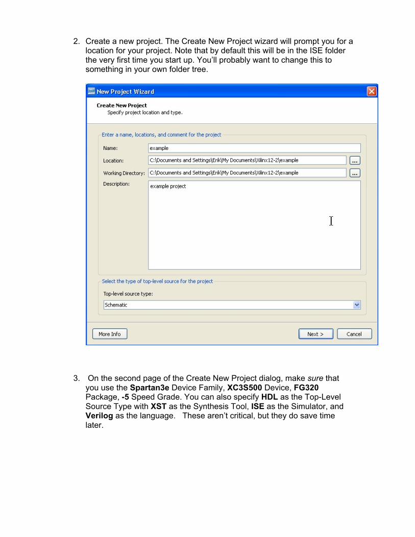
2. Create a new project. The Create New Project wizard will prompt you for a location for your project. Note that by default this will be in the ISE folder the very first time you start up. You’ll probably want to change this to something in your own folder tree.
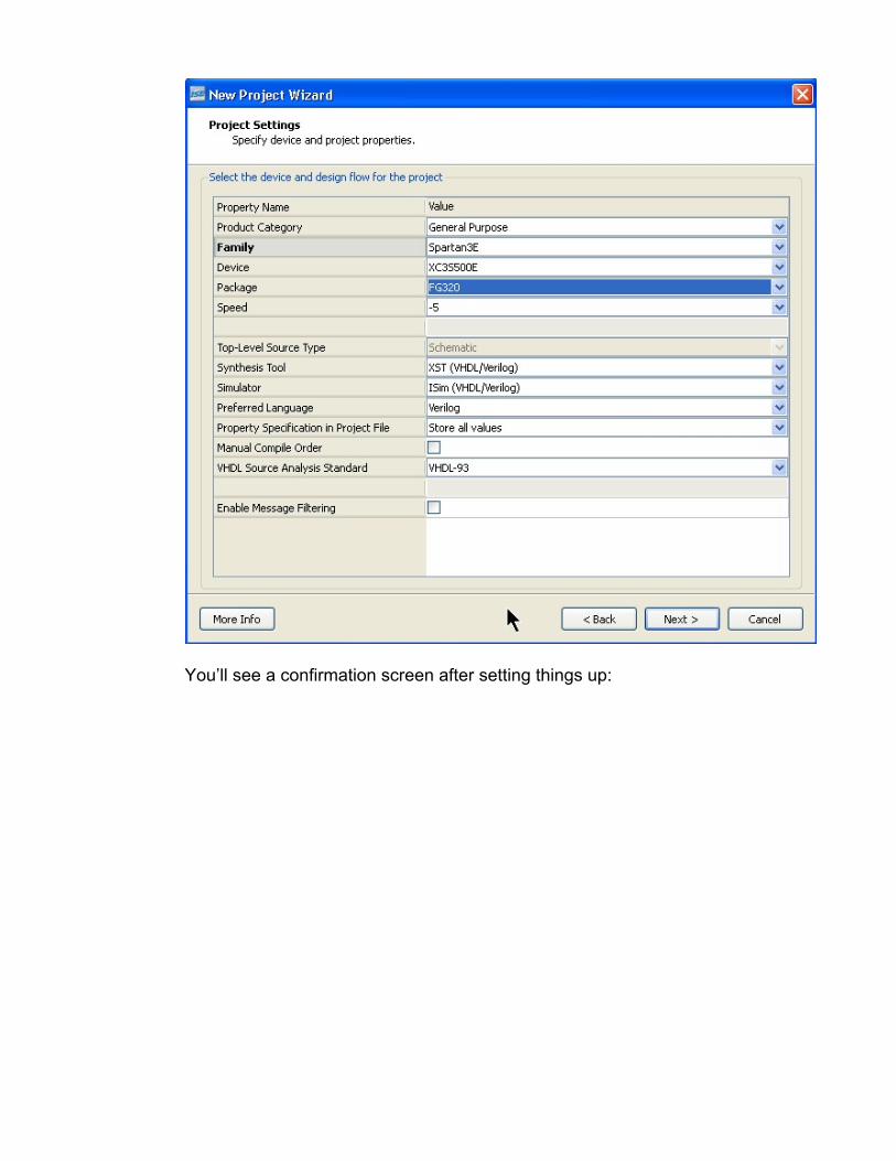
3. On the second page of the Create New Project dialog, make sure that you use the Spartan3e Device Family, XC3S500 Device, FG320 Package, -5 Speed Grade. You can also specify HDL as the Top-Level Source Type with XST as the Synthesis Tool, ISE as the Simulator, and Verilog as the language. These aren’t critical, but they do save time later.
You’ll see a confirmation screen after setting things up:
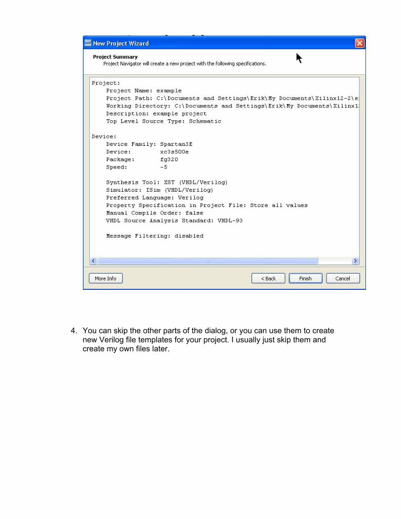
4. You can skip the other parts of the dialog, or you can use them to create new Verilog file templates for your project. I usually just skip them and create my own files later.
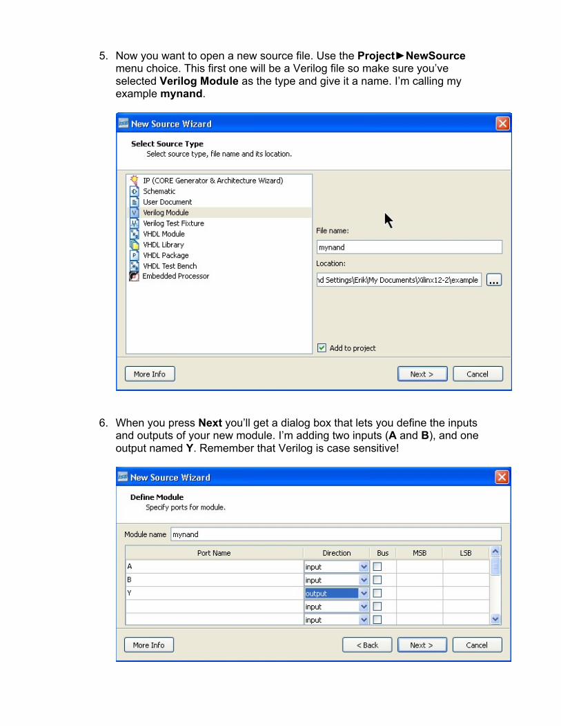
5. Now you want to open a new source file. Use the Project►NewSource menu choice. This first one will be a Verilog file so make sure you’ve selected Verilog Module as the type and give it a name. I’m calling my example mynand.
6. When you press Next you’ll get a dialog box that lets you define the inputs and outputs of your new module. I’m adding two inputs (A and B), and one output named Y. Remember that Verilog is case sensitive!
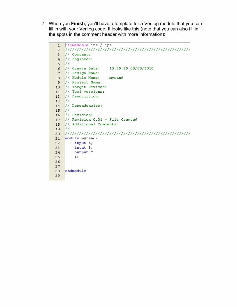
7. When you Finish, you’ll have a template for a Verilog module that you can fill in with your Verilog code. It looks like this (note that you can also fill in the spots in the comment header with more information):

8. Now you can fill in the rest of the Verilog module to implement some Boolean function. I’ll implement a NAND for this example. You can use any of the Verilog techniques that you know about. (see the Brown & Vranesic text from 3700, for example, or any number of Verilog tutorials on the web.) Note that ISE 10.1 uses Verilog 2001 syntax where the inputs and outputs are defined right in the argument definition line. I’ll use a continuous assignment statement: assign Y = ~(A & B); as shown below, then I’ll save the file.
9. In order to use this Verilog code in a schematic, you’ll need to create a schematic symbol. Select the mynand.v file in the Sources window, then in the Processes window select Create Schematic Symbol under the Design Utilities.
10. You now have a piece of Verilog that you can simulate and synthesize as is, or you can also use it in a schematic as a component.
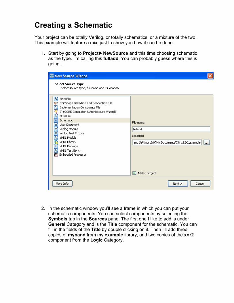
Creating a Schematic Your project can be totally Verilog, or totally schematics, or a mixture of the two. This example will feature a mix, just to show you how it can be done.
1. Start by going to Project►NewSource and this time choosing schematic as the type. I’m calling this fulladd. You can probably guess where this is going…
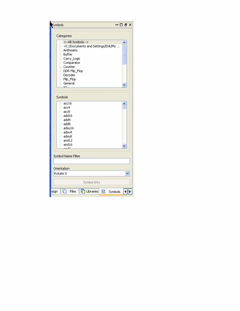
2. In the schematic window you’ll see a frame in which you can put your schematic components. You can select components by selecting the Symbols tab in the Sources pane. The first one I like to add is under General Category and is the Title component for the schematic. You can fill in the fields of the Title by double clicking on it. Then I’ll add three copies of mynand from my example library, and two copies of the xor2 component from the Logic Category.

3. Now I’ll use the wiring tool to connect up the components to make a Full Adder.
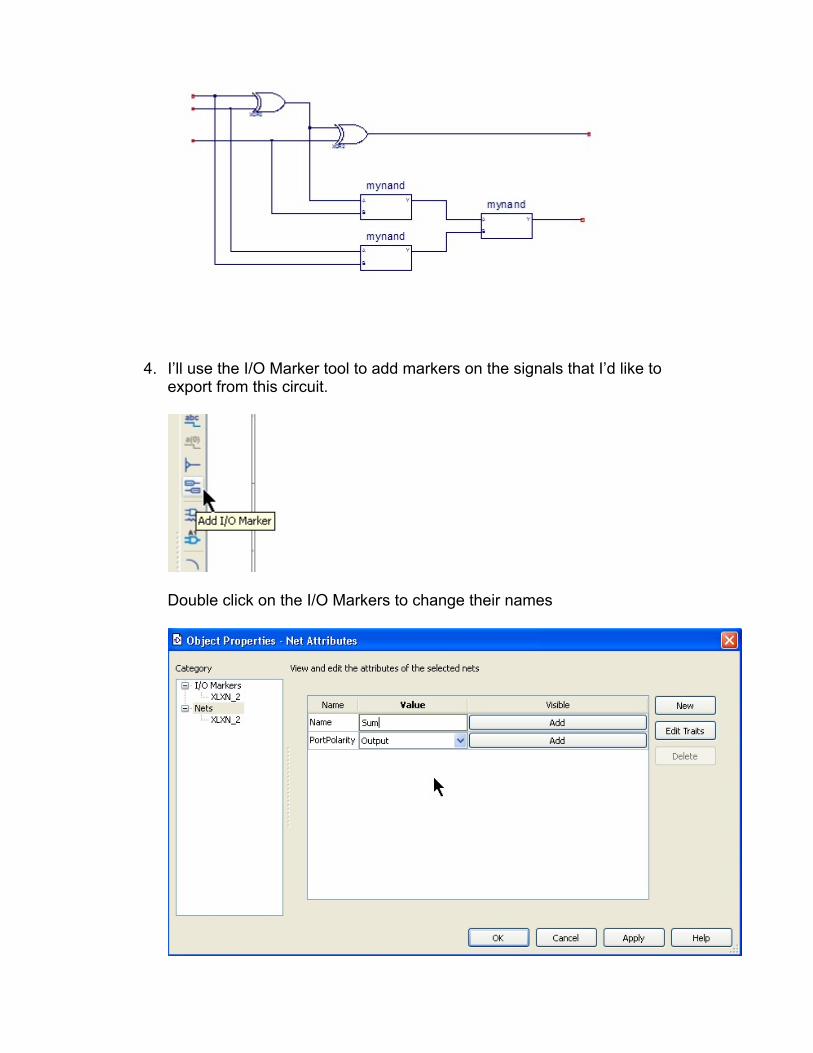
4. I’ll use the I/O Marker tool to add markers on the signals that I’d like to export from this circuit.
Double click on the I/O Markers to change their names
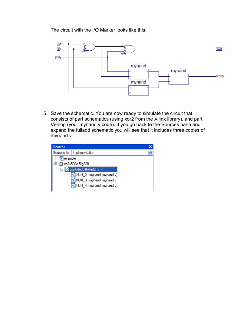
The circuit with the I/O Marker looks like this:
5. Save the schematic. You are now ready to simulate the circuit that consists of part schematics (using xor2 from the Xilinx library), and part Verilog (your mynand.v code). If you go back to the Sources pane and expand the fulladd schematic you will see that it includes three copies of mynand.v.
Simulating your Circuit: Now that you have a saved source file (fulladd is the top file in this case), you can simulate its behavior. We’ll use the ISE simulator with a testbench to drive the simulation. Note that the testbench files that drive the simulations are also Verilog files. To simulate the fulladd circuit:
1. Go to the top left pane (design) and change the View field to be Simulation. This changes the view to include sources that are interesting for simulation, and also changes the options in the bottom Processes pane to show the simulation options.
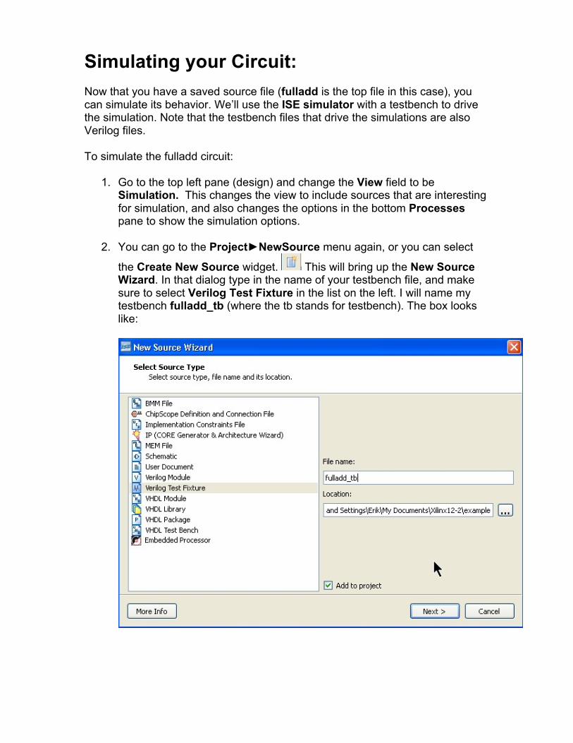
2. You can go to the Project►NewSource menu again, or you can select
the Create New Source widget. This will bring up the New Source Wizard. In that dialog type in the name of your testbench file, and make sure to select Verilog Test Fixture in the list on the left. I will name my testbench fulladd_tb (where the tb stands for testbench). The box looks like:
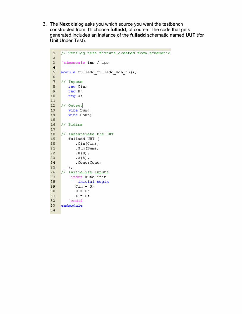
3. The Next dialog asks you which source you want the testbench constructed from. I’ll choose fulladd, of course. The code that gets generated includes an instance of the fulladd schematic named UUT (for Unit Under Test).
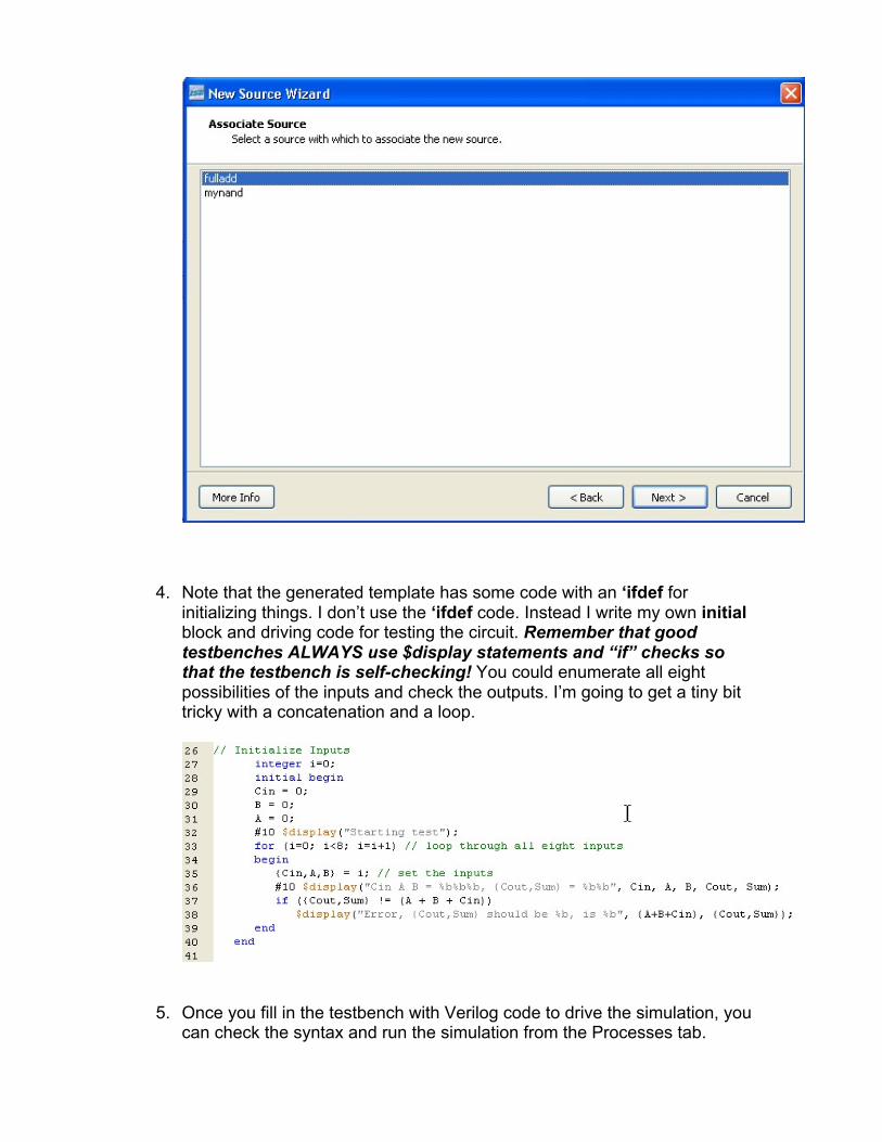
4. Note that the generated template has some code with an ‘ifdef for initializing things. I don’t use the ‘ifdef code. Instead I write my own initial block and driving code for testing the circuit. Remember that good testbenches ALWAYS use $display statements and “if” checks so that the testbench is self-checking! You could enumerate all eight possibilities of the inputs and check the outputs. I’m going to get a tiny bit tricky with a concatenation and a loop.
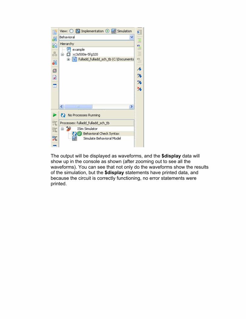
5. Once you fill in the testbench with Verilog code to drive the simulation, you can check the syntax and run the simulation from the Processes tab.
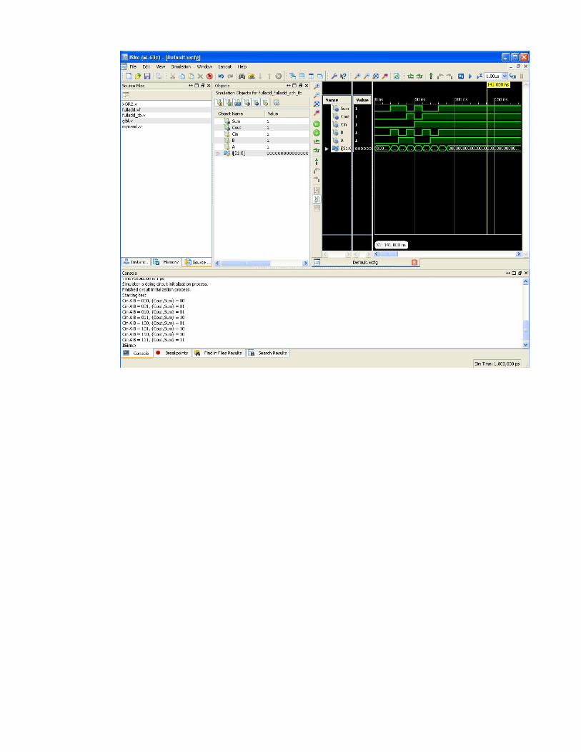
The output will be displayed as waveforms, and the $display data will show up in the console as shown (after zooming out to see all the waveforms). You can see that not only do the waveforms show the results of the simulation, but the $display statements have printed data, and because the circuit is correctly functioning, no error statements were printed.
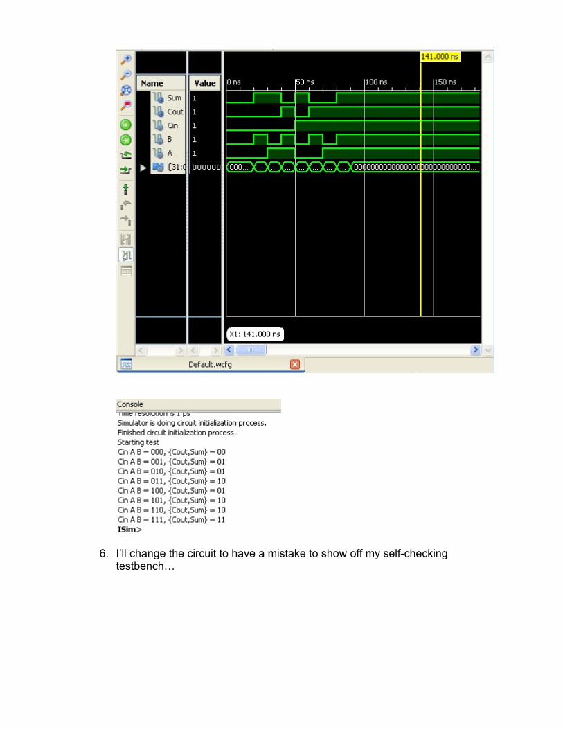
6. I’ll change the circuit to have a mistake to show off my self-checking testbench…
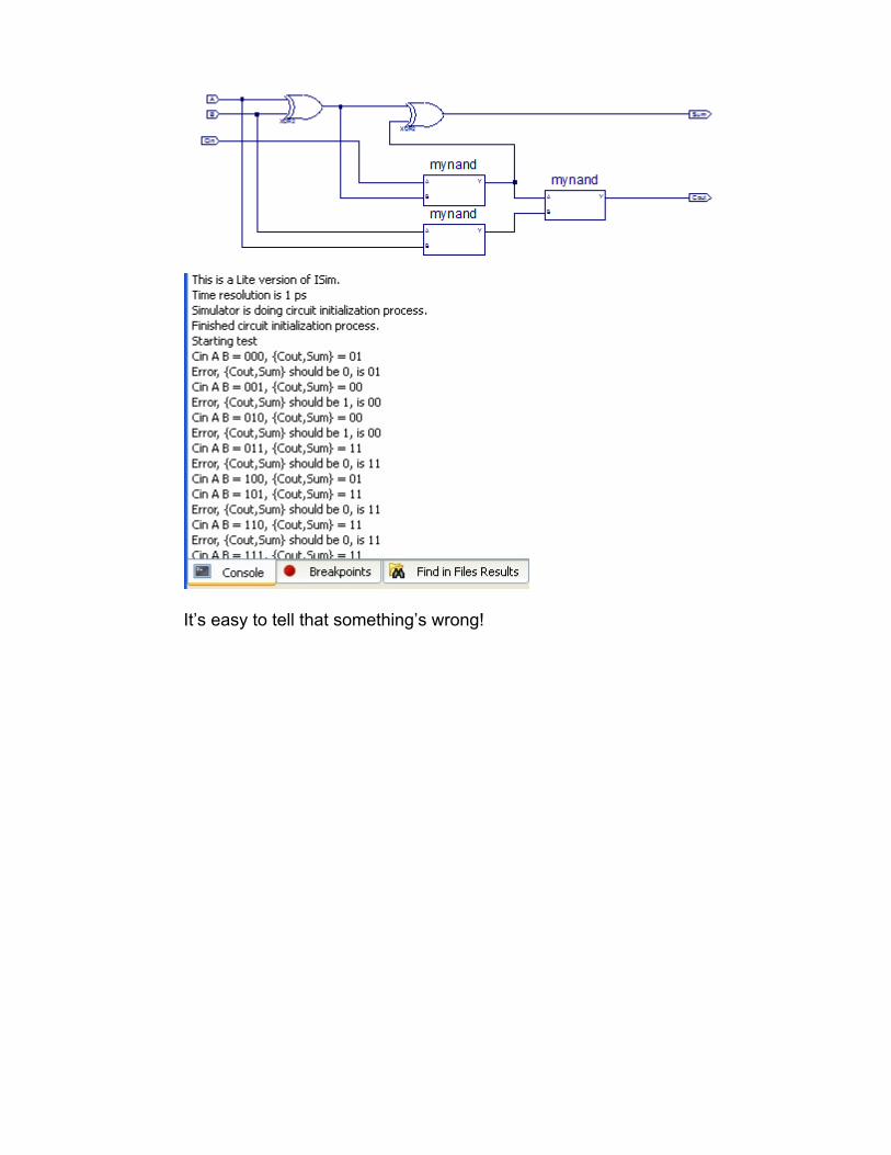
It’s easy to tell that something’s wrong!

Synthesizing your circuit to the Xilinx FPGA Now that you have a correctly simulating Verilog module, you will have the ISE (webPACK) tool synthesize your Verilog to something that can be mapped to the Xilinx FPGA. That is, the Verilog code will be converted by ISE to some gates that are on the FPGA. To be even more specific, ISE will convert the schematic/Verilog project description into a set of configuration bits that are used to program the Xilinx part. Those configuration bits are in a .bit file and are downloaded to the Xilinx part in this section of the tutorial. You will use your Spartan-3E board for this part of the tutorial. This is known as the “Spartan 3E Starter Kit” and is a board produced by Xilinx. It is a very feature-laden board with a Spartan 3e XC3S500E FPGA, 64Mbytes of SDRAM, 128Mbits of flash EPROM, A/D and D/A converters, RS232 drivers, VGA, PS/2, USB, and Ethernet connectors, a 16 character two-line LCD, and a lot more. You can get more info from Xilinx at http://www.xilinx.com/products/devkits/HW-SPAR3E-SK-US-G.htm

Specifically we will need to: • Assign A, B, and Y to the correct pins on the FPGA that connect to the
switches and LEDs on the S3E board • Synthesize the Verilog code into FPGA configuration • Generate a programming file with all this information (.bit file) • Use the impact tools from Xilinx (part of WebPACK) to configure the FPGA
through the USB connection.
1. Back in the Design pane, return to the Implementation view and select your fulladd schematic. Now in the bottom (Processes) pane you will see some options including User Constraints, Synthesize, and Implement Design. The first thing we’ll do is assign pins using the User Constraints tab. Expand that tab and select the I/O Pin Planning (PlanAhead) – Pre-Synthesis choice. This will let us assign our signals to pins on the Xilinx part using the PlanAhead tool.
Because we’re headed towards putting this on the Xilinx FPGA on the Spartan-3E board, we need to set some constraints. In particular, we need to tell ISE which pins on the Xilinx chip we want A, B, Cin assigned to so that we can access those from switches, and where we want Cout and Sum so we can see those on the LEDs on the Spartan-3E board. This will open a whole new tool called PlanAhead which you can use to set your pin constraints. You may have to agree to add a UCF (Universal Constraints File) file to your project. You should agree to this.
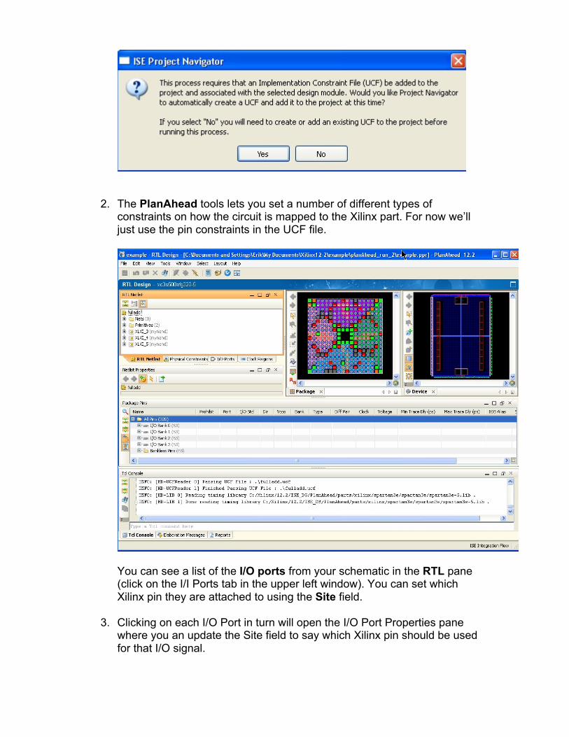
2. The PlanAhead tools lets you set a number of different types of constraints on how the circuit is mapped to the Xilinx part. For now we’ll just use the pin constraints in the UCF file.
You can see a list of the I/O ports from your schematic in the RTL pane (click on the I/I Ports tab in the upper left window). You can set which Xilinx pin they are attached to using the Site field.
3. Clicking on each I/O Port in turn will open the I/O Port Properties pane where you an update the Site field to say which Xilinx pin should be used for that I/O signal.
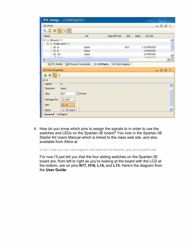
4. How do you know which pins to assign the signals to in order to use the switches and LEDs on the Spartan-3E board? You look in the Spartan-3E Starter Kit Users Manual which is linked to the class web site, and also available from Xilinx at http://www.xilinx.com/support/documentation/boards_and_kits/ug230.pdf
For now I’ll just tell you that the four sliding switches on the Spartan-3E board are, from left to right as you’re looking at the board with the LCD at the bottom, are on pins N17, H18, L14, and L13. Here’s the diagram from the User Guide:

and the UCF info is:
This tells you how to fill out the information in PlanAhead for the switches. I’ll put A, B and Cin on Sw3, Sw2, and Sw1.
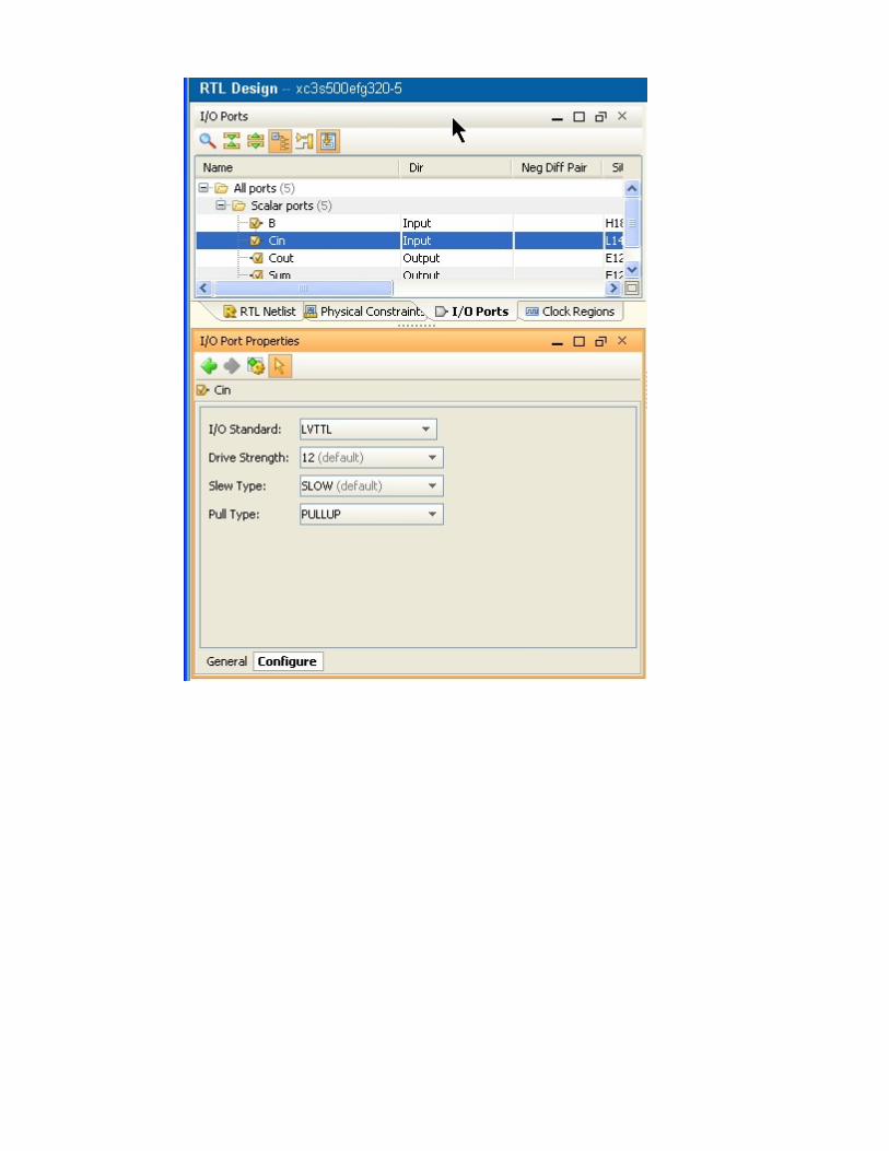
5. Note that you’ll have to click on Configure in the I/O Port Properties to set some of the parameters to be as specified in the User Guide.

6. The LEDs are also described in the User Guide:
I’ll use LED1 and LED0 as Cout and Sum. Note that it’s important to get all the details of the pins correct as they’re described in the manual! The switches won’t function properly without the pullup, for example, and the LEDs really need to have the drive strength set.
7. Now Save the PlanAhead settings. This will update things in your main ISE Webpack project.
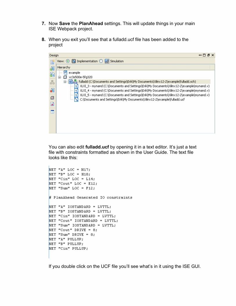
8. When you exit you’ll see that a fulladd.ucf file has been added to the project
You can also edit fulladd.ucf by opening it in a text editor. It’s just a text file with constraints formatted as shown in the User Guide. The text file looks like this:
If you double click on the UCF file you’ll see what’s in it using the ISE GUI.
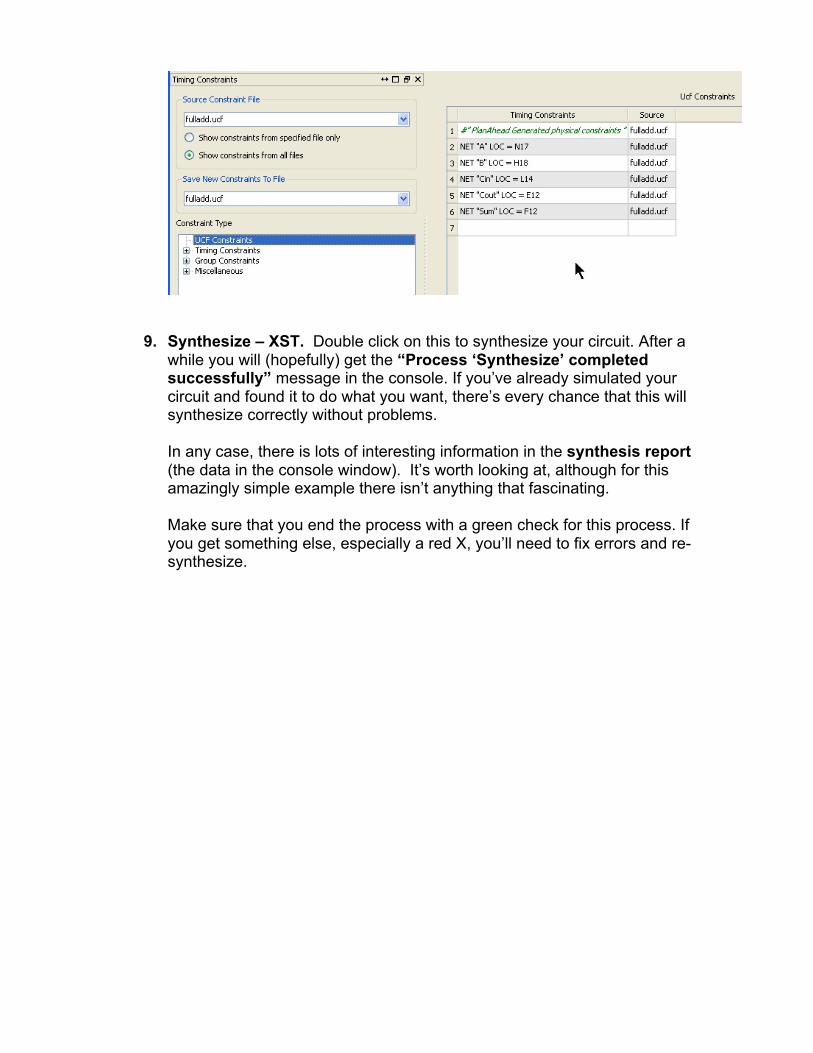
9. Synthesize – XST. Double click on this to synthesize your circuit. After a while you will (hopefully) get the “Process ‘Synthesize’ completed successfully” message in the console. If you’ve already simulated your circuit and found it to do what you want, there’s every chance that this will synthesize correctly without problems. In any case, there is lots of interesting information in the synthesis report (the data in the console window). It’s worth looking at, although for this amazingly simple example there isn’t anything that fascinating. Make sure that you end the process with a green check for this process. If you get something else, especially a red X, you’ll need to fix errors and re-synthesize.
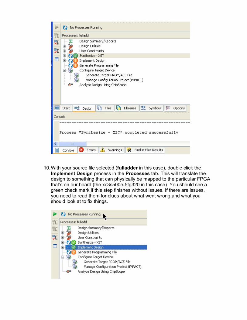
10. With your source file selected (fulladder in this case), double click the Implement Design process in the Processes tab. This will translate the design to something that can physically be mapped to the particular FPGA that’s on our board (the xc3s500e-5fg320 in this case). You should see a green check mark if this step finishes without issues. If there are issues, you need to read them for clues about what went wrong and what you should look at to fix things.

11. If you expand this Implement Design tab (which is not necessary) you will see that the Implement Design process actually consists of three parts:
a. Translate: Translate is the first step in the implementation process. The Translate process merges all of the input netlists and design constraint information and outputs a Xilinx NGD (Native Generic Database) file. The output NGD file can then be mapped to the targeted FPGA device.
b. Map: Mapping is the process of assigning a design’s logic elements to the specific physical elements that actually implement logic functions in a device. The Map process creates an NCD (Native Circuit Description) file. The NCD file will be used by the PAR process.
c. Place and Route (PAR): PAR uses the NCD file created by the Map process to place and route your design. PAR outputs an NCD file that is used by the bitstream generator (BitGen) to create a (.bit) file. The Bit file (see the next step) is what’s used to actually program the FPGA.
12. At this point you can look at the Design Summary to find out all sorts of things about your circuit. One thing that you might want to check is to click on the Pinout Report and check that your signals were correctly assigned to the pins you wanted them to be assigned to.

13. Now double click the process: Generate Programming File. This will generate the actual configuration bits into a .bit file that you can use to program your Spartan-3E board to behave like your circuit (in this case a full adder).
14. Now that you have the programming file, you can program the Spartan-3E board using the iMPACT tool and the USB cable on your PC/laptop. First, make sure that the jumpers on your Spartan-3E board are installed correctly. In particular, check that the configuration options are correctly set. The configuration options are at the top of the board near the RS232 interfaces.

The jumpers on the J30 headers must be set for JTAG programming. This means that only the middle pins of the header should have a jumper on them. See the following illustration from the User Guide. Your board should look like this!
15. Now that you have the jumpers set correctly, you can plug in the power to your Spartan-3E board, and connect the USB cable between the Spartan-3E and your PC. Then when you turn on the power, the PC should
recognize the Xilinx cable/board and install the drivers.
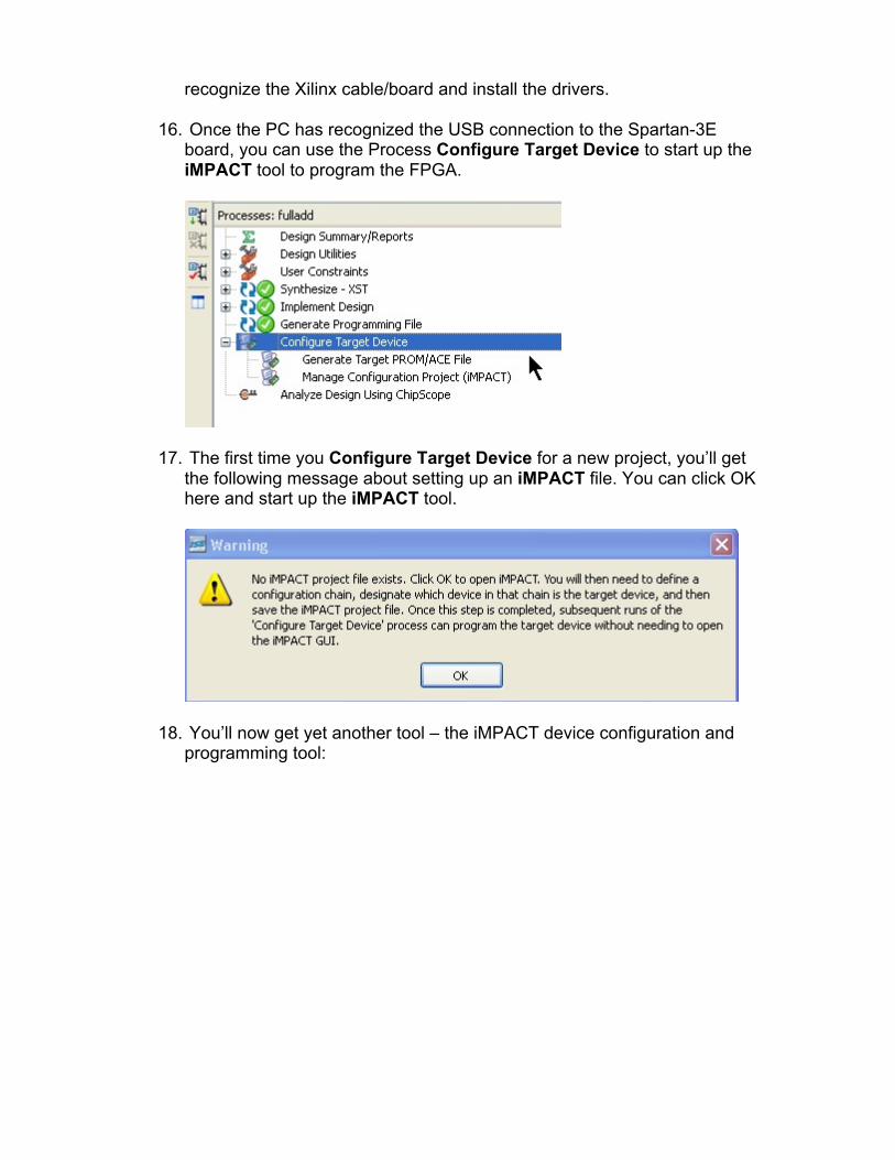
16. Once the PC has recognized the USB connection to the Spartan-3E board, you can use the Process Configure Target Device to start up the iMPACT tool to program the FPGA.
17. The first time you Configure Target Device for a new project, you’ll get the following message about setting up an iMPACT file. You can click OK here and start up the iMPACT tool.
18. You’ll now get yet another tool – the iMPACT device configuration and programming tool:
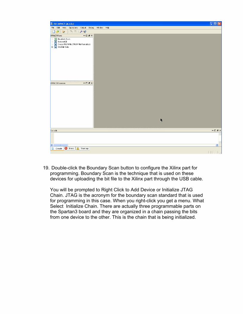
19. Double-click the Boundary Scan button to configure the Xilinx part for programming. Boundary Scan is the technique that is used on these devices for uploading the bit file to the Xilinx part through the USB cable. You will be prompted to Right Click to Add Device or Initialize JTAG Chain. JTAG is the acronym for the boundary scan standard that is used for programming in this case. When you right-click you get a menu. What Select Initialize Chain. There are actually three programmable parts on the Spartan3 board and they are organized in a chain passing the bits from one device to the other. This is the chain that is being initialized.
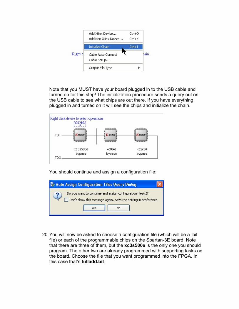
Note that you MUST have your board plugged in to the USB cable and turned on for this step! The initialization procedure sends a query out on the USB cable to see what chips are out there. If you have everything plugged in and turned on it will see the chips and initialize the chain.
You should continue and assign a configuration file:
20. You will now be asked to choose a configuration file (which will be a .bit file) or each of the programmable chips on the Spartan-3E board. Note that there are three of them, but the xc3s500e is the only one you should program. The other two are already programmed with supporting tasks on the board. Choose the file that you want programmed into the FPGA. In this case that’s fulladd.bit.
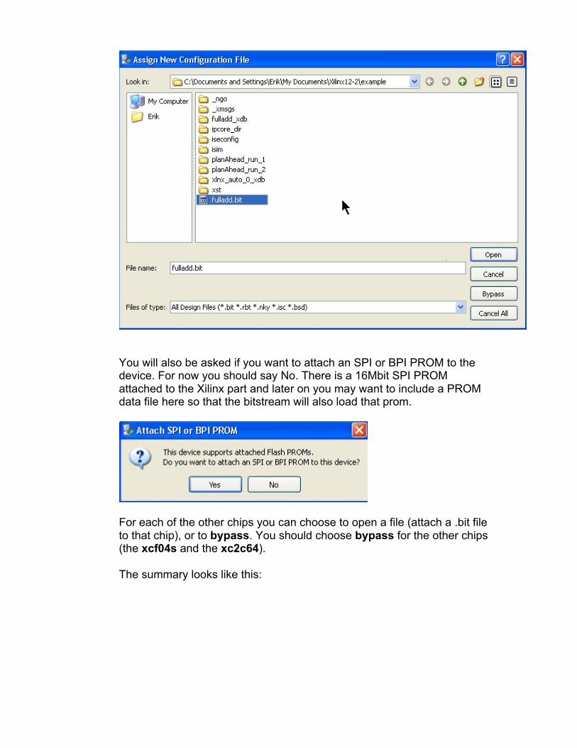
You will also be asked if you want to attach an SPI or BPI PROM to the device. For now you should say No. There is a 16Mbit SPI PROM attached to the Xilinx part and later on you may want to include a PROM data file here so that the bitstream will also load that prom.
For each of the other chips you can choose to open a file (attach a .bit file to that chip), or to bypass. You should choose bypass for the other chips (the xcf04s and the xc2c64). The summary looks like this:
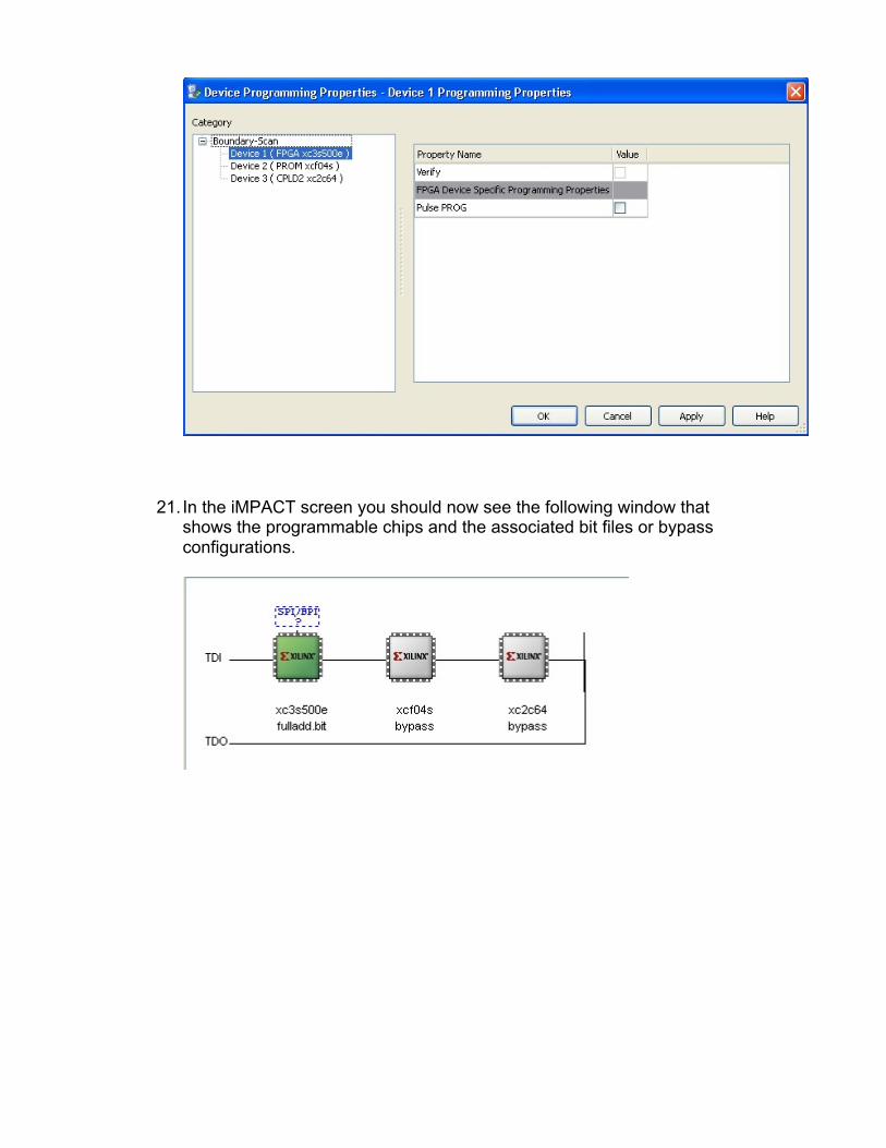
21. In the iMPACT screen you should now see the following window that shows the programmable chips and the associated bit files or bypass configurations.

22. Now you can select the Spartan-3E (the xc3s500e) and right click to get a dialog. Select Program in this dialog to program the FPGA.
You should see the following indication that the programming has succeeded. You should also see the xc-done LED (a little yellow LED underneath the J30 jumper on the board) light up if the programming is successful.
23. Your circuit should now be running on the Spartan-3E board. If you’ve followed this tutorial you should now be able to set the sw3, sw2, and sw1 switches and look for the full adder output on LDE1 and LED0.
24. If you make changes and want to reload the bit file to the FPGA (after making changes, for example), you can restart the iMPACT tool using the Manage Configuration Project (iMPACT) option under Configure Target Device.

You can then right click on the xc3s500e device and program it with the new bit file or use the iMPACT Processes in the lower left:
Whew! That’s it…

Overview of the Procedure
1. Design the circuit that you would like to map to the Xilinx part on the FPGA. You can use schematics, or Verilog, or a mixture of both.
2. Simulate your circuit using the ISE Simulator and a Verilog testbench to provide inputs to the circuit. Use “if” statements in your testbench to make it self-checking.
3. Generate a UCF file to hold constraints such as pin assignments (later we’ll use the UCF file for other constraints like timing and speed). Use the PlanAhead tool to generate this file.
4. Assign the I/O pins in your design to the pins on the FPGA that you want them connected to.
5. Synthesize the design for the FPGA using the XST synthesis tool.
6. Implement the design to map it to the specific FPGA on the Spartan-3E board
7. Generate the programming .bit file that has the bitstream that configures the FPGA.
8. Connect your Spartan3 board to the computer and use theiMPACT tool to program the FPGA using the bitstream. \